US20170033295A1 - Organic electroluminescent materials and devices - Google Patents
Organic electroluminescent materials and devices Download PDFInfo
- Publication number
- US20170033295A1 US20170033295A1 US15/173,806 US201615173806A US2017033295A1 US 20170033295 A1 US20170033295 A1 US 20170033295A1 US 201615173806 A US201615173806 A US 201615173806A US 2017033295 A1 US2017033295 A1 US 2017033295A1
- Authority
- US
- United States
- Prior art keywords
- group
- compound
- ring
- nitrogen
- emitting device
- Prior art date
- Legal status (The legal status is an assumption and is not a legal conclusion. Google has not performed a legal analysis and makes no representation as to the accuracy of the status listed.)
- Granted
Links
- 239000000463 material Substances 0.000 title claims abstract description 93
- 150000001875 compounds Chemical class 0.000 claims abstract description 90
- WIUZHVZUGQDRHZ-UHFFFAOYSA-N [1]benzothiolo[3,2-b]pyridine Chemical compound C1=CN=C2C3=CC=CC=C3SC2=C1 WIUZHVZUGQDRHZ-UHFFFAOYSA-N 0.000 claims abstract description 8
- 239000010410 layer Substances 0.000 claims description 102
- IJGRMHOSHXDMSA-UHFFFAOYSA-N Atomic nitrogen Chemical compound N#N IJGRMHOSHXDMSA-UHFFFAOYSA-N 0.000 claims description 47
- -1 amino, silyl Chemical group 0.000 claims description 41
- 229910052757 nitrogen Inorganic materials 0.000 claims description 39
- 125000003118 aryl group Chemical group 0.000 claims description 35
- 238000006467 substitution reaction Methods 0.000 claims description 31
- 239000003446 ligand Substances 0.000 claims description 29
- 125000001072 heteroaryl group Chemical group 0.000 claims description 28
- 239000012044 organic layer Substances 0.000 claims description 27
- JUJWROOIHBZHMG-UHFFFAOYSA-N Pyridine Chemical compound C1=CC=NC=C1 JUJWROOIHBZHMG-UHFFFAOYSA-N 0.000 claims description 22
- 125000000217 alkyl group Chemical group 0.000 claims description 22
- YZCKVEUIGOORGS-OUBTZVSYSA-N Deuterium Chemical compound [2H] YZCKVEUIGOORGS-OUBTZVSYSA-N 0.000 claims description 21
- 125000000753 cycloalkyl group Chemical group 0.000 claims description 21
- 229910052805 deuterium Inorganic materials 0.000 claims description 21
- 229910052739 hydrogen Inorganic materials 0.000 claims description 20
- 239000001257 hydrogen Substances 0.000 claims description 20
- 239000002019 doping agent Substances 0.000 claims description 19
- 125000003342 alkenyl group Chemical group 0.000 claims description 18
- 125000000304 alkynyl group Chemical group 0.000 claims description 18
- 125000003710 aryl alkyl group Chemical group 0.000 claims description 18
- 230000003111 delayed effect Effects 0.000 claims description 17
- 229910052760 oxygen Inorganic materials 0.000 claims description 17
- 230000000903 blocking effect Effects 0.000 claims description 16
- 229910052799 carbon Inorganic materials 0.000 claims description 16
- 125000000392 cycloalkenyl group Chemical group 0.000 claims description 16
- OKTJSMMVPCPJKN-UHFFFAOYSA-N Carbon Chemical compound [C] OKTJSMMVPCPJKN-UHFFFAOYSA-N 0.000 claims description 14
- 125000002252 acyl group Chemical group 0.000 claims description 14
- 125000003545 alkoxy group Chemical group 0.000 claims description 14
- 125000004104 aryloxy group Chemical group 0.000 claims description 14
- 125000002915 carbonyl group Chemical group [*:2]C([*:1])=O 0.000 claims description 14
- TXCDCPKCNAJMEE-UHFFFAOYSA-N dibenzofuran Chemical compound C1=CC=C2C3=CC=CC=C3OC2=C1 TXCDCPKCNAJMEE-UHFFFAOYSA-N 0.000 claims description 14
- 150000002148 esters Chemical class 0.000 claims description 14
- 125000004404 heteroalkyl group Chemical group 0.000 claims description 14
- 150000002527 isonitriles Chemical class 0.000 claims description 14
- 239000000203 mixture Substances 0.000 claims description 14
- 150000002825 nitriles Chemical class 0.000 claims description 14
- FVZVCSNXTFCBQU-UHFFFAOYSA-N phosphanyl Chemical group [PH2] FVZVCSNXTFCBQU-UHFFFAOYSA-N 0.000 claims description 14
- 125000000475 sulfinyl group Chemical group [*:2]S([*:1])=O 0.000 claims description 14
- 125000000472 sulfonyl group Chemical group *S(*)(=O)=O 0.000 claims description 14
- 125000003396 thiol group Chemical group [H]S* 0.000 claims description 14
- QJGQUHMNIGDVPM-UHFFFAOYSA-N nitrogen group Chemical group [N] QJGQUHMNIGDVPM-UHFFFAOYSA-N 0.000 claims description 13
- 229910052717 sulfur Inorganic materials 0.000 claims description 13
- UJOBWOGCFQCDNV-UHFFFAOYSA-N 9H-carbazole Chemical compound C1=CC=C2C3=CC=CC=C3NC2=C1 UJOBWOGCFQCDNV-UHFFFAOYSA-N 0.000 claims description 12
- 150000002431 hydrogen Chemical class 0.000 claims description 12
- 238000000034 method Methods 0.000 claims description 12
- 239000002800 charge carrier Substances 0.000 claims description 11
- 229910052736 halogen Inorganic materials 0.000 claims description 11
- 150000002367 halogens Chemical class 0.000 claims description 11
- UMJSCPRVCHMLSP-UHFFFAOYSA-N pyridine Natural products COC1=CC=CN=C1 UMJSCPRVCHMLSP-UHFFFAOYSA-N 0.000 claims description 11
- 125000004435 hydrogen atom Chemical group [H]* 0.000 claims description 9
- 150000001732 carboxylic acid derivatives Chemical class 0.000 claims description 8
- SLGBZMMZGDRARJ-UHFFFAOYSA-N Triphenylene Natural products C1=CC=C2C3=CC=CC=C3C3=CC=CC=C3C2=C1 SLGBZMMZGDRARJ-UHFFFAOYSA-N 0.000 claims description 7
- 229910052711 selenium Inorganic materials 0.000 claims description 7
- 150000001735 carboxylic acids Chemical class 0.000 claims description 6
- DHFABSXGNHDNCO-UHFFFAOYSA-N dibenzoselenophene Chemical compound C1=CC=C2C3=CC=CC=C3[se]C2=C1 DHFABSXGNHDNCO-UHFFFAOYSA-N 0.000 claims description 6
- 125000005580 triphenylene group Chemical group 0.000 claims description 6
- 238000009472 formulation Methods 0.000 claims description 5
- 230000008569 process Effects 0.000 claims description 5
- 230000005855 radiation Effects 0.000 claims description 4
- BPMFPOGUJAAYHL-UHFFFAOYSA-N 9H-Pyrido[2,3-b]indole Chemical compound C1=CC=C2C3=CC=CC=C3NC2=N1 BPMFPOGUJAAYHL-UHFFFAOYSA-N 0.000 claims description 2
- 125000003636 chemical group Chemical group 0.000 claims description 2
- 229910052723 transition metal Inorganic materials 0.000 claims description 2
- 150000003624 transition metals Chemical group 0.000 claims description 2
- 0 Cc1ccc(*)cc1 Chemical compound Cc1ccc(*)cc1 0.000 description 44
- 229910052751 metal Inorganic materials 0.000 description 17
- 239000002184 metal Substances 0.000 description 17
- 125000001424 substituent group Chemical group 0.000 description 13
- RAXXELZNTBOGNW-UHFFFAOYSA-N imidazole Natural products C1=CNC=N1 RAXXELZNTBOGNW-UHFFFAOYSA-N 0.000 description 12
- 150000003384 small molecules Chemical class 0.000 description 12
- 230000032258 transport Effects 0.000 description 12
- YMWUJEATGCHHMB-UHFFFAOYSA-N Dichloromethane Chemical compound ClCCl YMWUJEATGCHHMB-UHFFFAOYSA-N 0.000 description 11
- 238000004770 highest occupied molecular orbital Methods 0.000 description 11
- 238000004768 lowest unoccupied molecular orbital Methods 0.000 description 11
- UFWIBTONFRDIAS-UHFFFAOYSA-N Naphthalene Chemical compound C1=CC=CC2=CC=CC=C21 UFWIBTONFRDIAS-UHFFFAOYSA-N 0.000 description 10
- 230000004888 barrier function Effects 0.000 description 10
- 125000004432 carbon atom Chemical group C* 0.000 description 10
- UHOVQNZJYSORNB-UHFFFAOYSA-N Benzene Chemical compound C1=CC=CC=C1 UHOVQNZJYSORNB-UHFFFAOYSA-N 0.000 description 9
- XSCHRSMBECNVNS-UHFFFAOYSA-N quinoxaline Chemical compound N1=CC=NC2=CC=CC=C21 XSCHRSMBECNVNS-UHFFFAOYSA-N 0.000 description 9
- 239000000243 solution Substances 0.000 description 9
- ZUOUZKKEUPVFJK-UHFFFAOYSA-N diphenyl Chemical compound C1=CC=CC=C1C1=CC=CC=C1 ZUOUZKKEUPVFJK-UHFFFAOYSA-N 0.000 description 8
- 239000007924 injection Substances 0.000 description 8
- 238000002347 injection Methods 0.000 description 8
- 239000000758 substrate Substances 0.000 description 8
- 238000000151 deposition Methods 0.000 description 7
- IYYZUPMFVPLQIF-UHFFFAOYSA-N dibenzothiophene sulfoxide Natural products C1=CC=C2C3=CC=CC=C3SC2=C1 IYYZUPMFVPLQIF-UHFFFAOYSA-N 0.000 description 7
- 230000005525 hole transport Effects 0.000 description 7
- YLQBMQCUIZJEEH-UHFFFAOYSA-N tetrahydrofuran Natural products C=1C=COC=1 YLQBMQCUIZJEEH-UHFFFAOYSA-N 0.000 description 7
- FCEHBMOGCRZNNI-UHFFFAOYSA-N 1-benzothiophene Chemical compound C1=CC=C2SC=CC2=C1 FCEHBMOGCRZNNI-UHFFFAOYSA-N 0.000 description 6
- SIKJAQJRHWYJAI-UHFFFAOYSA-N Indole Chemical compound C1=CC=C2NC=CC2=C1 SIKJAQJRHWYJAI-UHFFFAOYSA-N 0.000 description 6
- IMNFDUFMRHMDMM-UHFFFAOYSA-N N-Heptane Chemical compound CCCCCCC IMNFDUFMRHMDMM-UHFFFAOYSA-N 0.000 description 6
- CTQNGGLPUBDAKN-UHFFFAOYSA-N O-Xylene Chemical group CC1=CC=CC=C1C CTQNGGLPUBDAKN-UHFFFAOYSA-N 0.000 description 6
- PCNDJXKNXGMECE-UHFFFAOYSA-N Phenazine Natural products C1=CC=CC2=NC3=CC=CC=C3N=C21 PCNDJXKNXGMECE-UHFFFAOYSA-N 0.000 description 6
- KYQCOXFCLRTKLS-UHFFFAOYSA-N Pyrazine Chemical compound C1=CN=CC=N1 KYQCOXFCLRTKLS-UHFFFAOYSA-N 0.000 description 6
- SMWDFEZZVXVKRB-UHFFFAOYSA-N Quinoline Chemical compound N1=CC=CC2=CC=CC=C21 SMWDFEZZVXVKRB-UHFFFAOYSA-N 0.000 description 6
- YTPLMLYBLZKORZ-UHFFFAOYSA-N Thiophene Chemical compound C=1C=CSC=1 YTPLMLYBLZKORZ-UHFFFAOYSA-N 0.000 description 6
- YXFVVABEGXRONW-UHFFFAOYSA-N Toluene Chemical compound CC1=CC=CC=C1 YXFVVABEGXRONW-UHFFFAOYSA-N 0.000 description 6
- DZBUGLKDJFMEHC-UHFFFAOYSA-N acridine Chemical compound C1=CC=CC2=CC3=CC=CC=C3N=C21 DZBUGLKDJFMEHC-UHFFFAOYSA-N 0.000 description 6
- MWPLVEDNUUSJAV-UHFFFAOYSA-N anthracene Chemical compound C1=CC=CC2=CC3=CC=CC=C3C=C21 MWPLVEDNUUSJAV-UHFFFAOYSA-N 0.000 description 6
- CUFNKYGDVFVPHO-UHFFFAOYSA-N azulene Chemical compound C1=CC=CC2=CC=CC2=C1 CUFNKYGDVFVPHO-UHFFFAOYSA-N 0.000 description 6
- IOJUPLGTWVMSFF-UHFFFAOYSA-N benzothiazole Chemical compound C1=CC=C2SC=NC2=C1 IOJUPLGTWVMSFF-UHFFFAOYSA-N 0.000 description 6
- WDECIBYCCFPHNR-UHFFFAOYSA-N chrysene Chemical compound C1=CC=CC2=CC=C3C4=CC=CC=C4C=CC3=C21 WDECIBYCCFPHNR-UHFFFAOYSA-N 0.000 description 6
- AWJUIBRHMBBTKR-UHFFFAOYSA-N isoquinoline Chemical compound C1=NC=CC2=CC=CC=C21 AWJUIBRHMBBTKR-UHFFFAOYSA-N 0.000 description 6
- 150000002894 organic compounds Chemical class 0.000 description 6
- 239000011368 organic material Substances 0.000 description 6
- YNPNZTXNASCQKK-UHFFFAOYSA-N phenanthrene Chemical compound C1=CC=C2C3=CC=CC=C3C=CC2=C1 YNPNZTXNASCQKK-UHFFFAOYSA-N 0.000 description 6
- BBEAQIROQSPTKN-UHFFFAOYSA-N pyrene Chemical compound C1=CC=C2C=CC3=CC=CC4=CC=C1C2=C43 BBEAQIROQSPTKN-UHFFFAOYSA-N 0.000 description 6
- MFRIHAYPQRLWNB-UHFFFAOYSA-N sodium tert-butoxide Chemical compound [Na+].CC(C)(C)[O-] MFRIHAYPQRLWNB-UHFFFAOYSA-N 0.000 description 6
- LFQSCWFLJHTTHZ-UHFFFAOYSA-N Ethanol Chemical compound CCO LFQSCWFLJHTTHZ-UHFFFAOYSA-N 0.000 description 5
- 125000004122 cyclic group Chemical group 0.000 description 5
- 239000000412 dendrimer Substances 0.000 description 5
- 229920000736 dendritic polymer Polymers 0.000 description 5
- 239000012634 fragment Substances 0.000 description 5
- 150000004820 halides Chemical class 0.000 description 5
- 125000000623 heterocyclic group Chemical group 0.000 description 5
- VVVPGLRKXQSQSZ-UHFFFAOYSA-N indolo[3,2-c]carbazole Chemical compound C1=CC=CC2=NC3=C4C5=CC=CC=C5N=C4C=CC3=C21 VVVPGLRKXQSQSZ-UHFFFAOYSA-N 0.000 description 5
- 230000005693 optoelectronics Effects 0.000 description 5
- 229920000642 polymer Polymers 0.000 description 5
- 239000007787 solid Substances 0.000 description 5
- VNFWTIYUKDMAOP-UHFFFAOYSA-N sphos Chemical compound COC1=CC=CC(OC)=C1C1=CC=CC=C1P(C1CCCCC1)C1CCCCC1 VNFWTIYUKDMAOP-UHFFFAOYSA-N 0.000 description 5
- JYEUMXHLPRZUAT-UHFFFAOYSA-N 1,2,3-triazine Chemical compound C1=CN=NN=C1 JYEUMXHLPRZUAT-UHFFFAOYSA-N 0.000 description 4
- YJTKZCDBKVTVBY-UHFFFAOYSA-N 1,3-Diphenylbenzene Chemical group C1=CC=CC=C1C1=CC=CC(C=2C=CC=CC=2)=C1 YJTKZCDBKVTVBY-UHFFFAOYSA-N 0.000 description 4
- HYZJCKYKOHLVJF-UHFFFAOYSA-N 1H-benzimidazole Chemical compound C1=CC=C2NC=NC2=C1 HYZJCKYKOHLVJF-UHFFFAOYSA-N 0.000 description 4
- XUIMIQQOPSSXEZ-UHFFFAOYSA-N Silicon Chemical compound [Si] XUIMIQQOPSSXEZ-UHFFFAOYSA-N 0.000 description 4
- 125000006615 aromatic heterocyclic group Chemical group 0.000 description 4
- 125000004429 atom Chemical group 0.000 description 4
- 230000015572 biosynthetic process Effects 0.000 description 4
- 239000004305 biphenyl Substances 0.000 description 4
- 235000010290 biphenyl Nutrition 0.000 description 4
- 150000004696 coordination complex Chemical class 0.000 description 4
- RMBPEFMHABBEKP-UHFFFAOYSA-N fluorene Chemical compound C1=CC=C2C3=C[CH]C=CC3=CC2=C1 RMBPEFMHABBEKP-UHFFFAOYSA-N 0.000 description 4
- 229960005544 indolocarbazole Drugs 0.000 description 4
- NIHNNTQXNPWCJQ-UHFFFAOYSA-N o-biphenylenemethane Natural products C1=CC=C2CC3=CC=CC=C3C2=C1 NIHNNTQXNPWCJQ-UHFFFAOYSA-N 0.000 description 4
- 125000001997 phenyl group Chemical group [H]C1=C([H])C([H])=C(*)C([H])=C1[H] 0.000 description 4
- 229910052698 phosphorus Inorganic materials 0.000 description 4
- 229910052710 silicon Inorganic materials 0.000 description 4
- 239000002904 solvent Substances 0.000 description 4
- 238000003786 synthesis reaction Methods 0.000 description 4
- KTZQTRPPVKQPFO-UHFFFAOYSA-N 1,2-benzoxazole Chemical compound C1=CC=C2C=NOC2=C1 KTZQTRPPVKQPFO-UHFFFAOYSA-N 0.000 description 3
- BCMCBBGGLRIHSE-UHFFFAOYSA-N 1,3-benzoxazole Chemical compound C1=CC=C2OC=NC2=C1 BCMCBBGGLRIHSE-UHFFFAOYSA-N 0.000 description 3
- FLBAYUMRQUHISI-UHFFFAOYSA-N 1,8-naphthyridine Chemical compound N1=CC=CC2=CC=CN=C21 FLBAYUMRQUHISI-UHFFFAOYSA-N 0.000 description 3
- BNRDGHFESOHOBF-UHFFFAOYSA-N 1-benzoselenophene Chemical compound C1=CC=C2[se]C=CC2=C1 BNRDGHFESOHOBF-UHFFFAOYSA-N 0.000 description 3
- WJFKNYWRSNBZNX-UHFFFAOYSA-N 10H-phenothiazine Chemical compound C1=CC=C2NC3=CC=CC=C3SC2=C1 WJFKNYWRSNBZNX-UHFFFAOYSA-N 0.000 description 3
- TZMSYXZUNZXBOL-UHFFFAOYSA-N 10H-phenoxazine Chemical compound C1=CC=C2NC3=CC=CC=C3OC2=C1 TZMSYXZUNZXBOL-UHFFFAOYSA-N 0.000 description 3
- BAXOFTOLAUCFNW-UHFFFAOYSA-N 1H-indazole Chemical compound C1=CC=C2C=NNC2=C1 BAXOFTOLAUCFNW-UHFFFAOYSA-N 0.000 description 3
- VEPOHXYIFQMVHW-XOZOLZJESA-N 2,3-dihydroxybutanedioic acid (2S,3S)-3,4-dimethyl-2-phenylmorpholine Chemical compound OC(C(O)C(O)=O)C(O)=O.C[C@H]1[C@@H](OCCN1C)c1ccccc1 VEPOHXYIFQMVHW-XOZOLZJESA-N 0.000 description 3
- OLGGLCIDAMICTA-UHFFFAOYSA-N 2-pyridin-2-yl-1h-indole Chemical compound N1C2=CC=CC=C2C=C1C1=CC=CC=N1 OLGGLCIDAMICTA-UHFFFAOYSA-N 0.000 description 3
- QMEQBOSUJUOXMX-UHFFFAOYSA-N 2h-oxadiazine Chemical compound N1OC=CC=N1 QMEQBOSUJUOXMX-UHFFFAOYSA-N 0.000 description 3
- BCHZICNRHXRCHY-UHFFFAOYSA-N 2h-oxazine Chemical compound N1OC=CC=C1 BCHZICNRHXRCHY-UHFFFAOYSA-N 0.000 description 3
- BWCDLEQTELFBAW-UHFFFAOYSA-N 3h-dioxazole Chemical compound N1OOC=C1 BWCDLEQTELFBAW-UHFFFAOYSA-N 0.000 description 3
- GJCOSYZMQJWQCA-UHFFFAOYSA-N 9H-xanthene Chemical compound C1=CC=C2CC3=CC=CC=C3OC2=C1 GJCOSYZMQJWQCA-UHFFFAOYSA-N 0.000 description 3
- XEKOWRVHYACXOJ-UHFFFAOYSA-N Ethyl acetate Chemical compound CCOC(C)=O XEKOWRVHYACXOJ-UHFFFAOYSA-N 0.000 description 3
- ZCQWOFVYLHDMMC-UHFFFAOYSA-N Oxazole Chemical compound C1=COC=N1 ZCQWOFVYLHDMMC-UHFFFAOYSA-N 0.000 description 3
- WTKZEGDFNFYCGP-UHFFFAOYSA-N Pyrazole Chemical compound C=1C=NNC=1 WTKZEGDFNFYCGP-UHFFFAOYSA-N 0.000 description 3
- CZPWVGJYEJSRLH-UHFFFAOYSA-N Pyrimidine Chemical compound C1=CN=CN=C1 CZPWVGJYEJSRLH-UHFFFAOYSA-N 0.000 description 3
- VYPSYNLAJGMNEJ-UHFFFAOYSA-N Silicium dioxide Chemical compound O=[Si]=O VYPSYNLAJGMNEJ-UHFFFAOYSA-N 0.000 description 3
- FZWLAAWBMGSTSO-UHFFFAOYSA-N Thiazole Chemical compound C1=CSC=N1 FZWLAAWBMGSTSO-UHFFFAOYSA-N 0.000 description 3
- FBVBNCGJVKIEHH-UHFFFAOYSA-N [1]benzofuro[3,2-b]pyridine Chemical compound C1=CN=C2C3=CC=CC=C3OC2=C1 FBVBNCGJVKIEHH-UHFFFAOYSA-N 0.000 description 3
- QZLAKPGRUFFNRD-UHFFFAOYSA-N [1]benzoselenolo[3,2-b]pyridine Chemical compound C1=CN=C2C3=CC=CC=C3[se]C2=C1 QZLAKPGRUFFNRD-UHFFFAOYSA-N 0.000 description 3
- RFRXIWQYSOIBDI-UHFFFAOYSA-N benzarone Chemical compound CCC=1OC2=CC=CC=C2C=1C(=O)C1=CC=C(O)C=C1 RFRXIWQYSOIBDI-UHFFFAOYSA-N 0.000 description 3
- WCZVZNOTHYJIEI-UHFFFAOYSA-N cinnoline Chemical compound N1=NC=CC2=CC=CC=C21 WCZVZNOTHYJIEI-UHFFFAOYSA-N 0.000 description 3
- 238000010586 diagram Methods 0.000 description 3
- GVEPBJHOBDJJJI-UHFFFAOYSA-N fluoranthrene Natural products C1=CC(C2=CC=CC=C22)=C3C2=CC=CC3=C1 GVEPBJHOBDJJJI-UHFFFAOYSA-N 0.000 description 3
- PZOUSPYUWWUPPK-UHFFFAOYSA-N indole Natural products CC1=CC=CC2=C1C=CN2 PZOUSPYUWWUPPK-UHFFFAOYSA-N 0.000 description 3
- RKJUIXBNRJVNHR-UHFFFAOYSA-N indolenine Natural products C1=CC=C2CC=NC2=C1 RKJUIXBNRJVNHR-UHFFFAOYSA-N 0.000 description 3
- QDLAGTHXVHQKRE-UHFFFAOYSA-N lichenxanthone Natural products COC1=CC(O)=C2C(=O)C3=C(C)C=C(OC)C=C3OC2=C1 QDLAGTHXVHQKRE-UHFFFAOYSA-N 0.000 description 3
- 239000011159 matrix material Substances 0.000 description 3
- 230000007246 mechanism Effects 0.000 description 3
- 125000004433 nitrogen atom Chemical group N* 0.000 description 3
- 229940078552 o-xylene Drugs 0.000 description 3
- WCPAKWJPBJAGKN-UHFFFAOYSA-N oxadiazole Chemical compound C1=CON=N1 WCPAKWJPBJAGKN-UHFFFAOYSA-N 0.000 description 3
- AZHVQJLDOFKHPZ-UHFFFAOYSA-N oxathiazine Chemical compound O1SN=CC=C1 AZHVQJLDOFKHPZ-UHFFFAOYSA-N 0.000 description 3
- CQDAMYNQINDRQC-UHFFFAOYSA-N oxatriazole Chemical compound C1=NN=NO1 CQDAMYNQINDRQC-UHFFFAOYSA-N 0.000 description 3
- 125000002080 perylenyl group Chemical group C1(=CC=C2C=CC=C3C4=CC=CC5=CC=CC(C1=C23)=C45)* 0.000 description 3
- CSHWQDPOILHKBI-UHFFFAOYSA-N peryrene Natural products C1=CC(C2=CC=CC=3C2=C2C=CC=3)=C3C2=CC=CC3=C1 CSHWQDPOILHKBI-UHFFFAOYSA-N 0.000 description 3
- NQFOGDIWKQWFMN-UHFFFAOYSA-N phenalene Chemical compound C1=CC([CH]C=C2)=C3C2=CC=CC3=C1 NQFOGDIWKQWFMN-UHFFFAOYSA-N 0.000 description 3
- 229950000688 phenothiazine Drugs 0.000 description 3
- LFSXCDWNBUNEEM-UHFFFAOYSA-N phthalazine Chemical compound C1=NN=CC2=CC=CC=C21 LFSXCDWNBUNEEM-UHFFFAOYSA-N 0.000 description 3
- CPNGPNLZQNNVQM-UHFFFAOYSA-N pteridine Chemical compound N1=CN=CC2=NC=CN=C21 CPNGPNLZQNNVQM-UHFFFAOYSA-N 0.000 description 3
- PBMFSQRYOILNGV-UHFFFAOYSA-N pyridazine Chemical compound C1=CC=NN=C1 PBMFSQRYOILNGV-UHFFFAOYSA-N 0.000 description 3
- JWVCLYRUEFBMGU-UHFFFAOYSA-N quinazoline Chemical compound N1=CN=CC2=CC=CC=C21 JWVCLYRUEFBMGU-UHFFFAOYSA-N 0.000 description 3
- 239000000741 silica gel Substances 0.000 description 3
- 229910002027 silica gel Inorganic materials 0.000 description 3
- 239000000126 substance Substances 0.000 description 3
- 238000002207 thermal evaporation Methods 0.000 description 3
- VLLMWSRANPNYQX-UHFFFAOYSA-N thiadiazole Chemical compound C1=CSN=N1.C1=CSN=N1 VLLMWSRANPNYQX-UHFFFAOYSA-N 0.000 description 3
- 229930192474 thiophene Natural products 0.000 description 3
- 150000003852 triazoles Chemical class 0.000 description 3
- GKTLHQFSIDFAJH-UHFFFAOYSA-N 3-(9h-carbazol-3-yl)-9-phenylcarbazole Chemical compound C1=CC=CC=C1N1C2=CC=C(C=3C=C4C5=CC=CC=C5NC4=CC=3)C=C2C2=CC=CC=C21 GKTLHQFSIDFAJH-UHFFFAOYSA-N 0.000 description 2
- KKPMGTFMIQSASU-UHFFFAOYSA-N 6-chloro-[1]benzothiolo[2,3-c]quinoline Chemical compound C12=CC=CC=C2SC2=C1C1=CC=CC=C1N=C2Cl KKPMGTFMIQSASU-UHFFFAOYSA-N 0.000 description 2
- ZOXJGFHDIHLPTG-UHFFFAOYSA-N Boron Chemical group [B] ZOXJGFHDIHLPTG-UHFFFAOYSA-N 0.000 description 2
- NNPPMTNAJDCUHE-UHFFFAOYSA-N CC(C)C Chemical compound CC(C)C NNPPMTNAJDCUHE-UHFFFAOYSA-N 0.000 description 2
- KIJOMOJYLMYLCA-UHFFFAOYSA-N CC1=CC=C(N2C3=CC=CC=C3C3=C/C4=C(\C=C/32)C2=C(C=CC=C2)O4)C=C1.CC1=CC=C(N2C3=CC=CC=C3C3=C/C4=C(\C=C/32)OC2=C4C=CC=C2)C=C1.CC1=CC=C(N2C3=CC=CC=C3C3=C4\OC5=C(C=CC=C5)\C4=C\C=C\32)C=C1.CN1C2=CC=CC=C2C2=C3/C4=C(C=CC=C4)O/C3=C3\C=CC=C\C3=C\21.CN1C2=CC=CC=C2C2=C3/OC4=C(C=CC=C4)/C3=C3\C=CC=C\C3=C\21 Chemical compound CC1=CC=C(N2C3=CC=CC=C3C3=C/C4=C(\C=C/32)C2=C(C=CC=C2)O4)C=C1.CC1=CC=C(N2C3=CC=CC=C3C3=C/C4=C(\C=C/32)OC2=C4C=CC=C2)C=C1.CC1=CC=C(N2C3=CC=CC=C3C3=C4\OC5=C(C=CC=C5)\C4=C\C=C\32)C=C1.CN1C2=CC=CC=C2C2=C3/C4=C(C=CC=C4)O/C3=C3\C=CC=C\C3=C\21.CN1C2=CC=CC=C2C2=C3/OC4=C(C=CC=C4)/C3=C3\C=CC=C\C3=C\21 KIJOMOJYLMYLCA-UHFFFAOYSA-N 0.000 description 2
- VZMOLHUOWJOWME-UHFFFAOYSA-N CC1=CC=C(N2C3=CC=CC=C3C3=C/C=C/C(C4=CC=C(C5=CC=CC=C5)C=C4)=C\32)C=C1.CC1=CC=CC(C2=CC(N3C4=CC=CC=C4C4=C/C=C/C=C\43)=CC=C2)=C1.CC1=CC=CC(N2C3=CC=CC=C3C3=C/C=C/C(C4=CC=C(C5=CC=CC=C5)C=C4)=C\32)=C1.CN1C2=CC=CC=C2C2=C/C=C/C(C3=CC=C(C4=CC=CC=C4)C=C3)=C\21.CN1C2=CC=CC=C2C2=C/C=C/C(C3=CC=CC=C3)=C\21 Chemical compound CC1=CC=C(N2C3=CC=CC=C3C3=C/C=C/C(C4=CC=C(C5=CC=CC=C5)C=C4)=C\32)C=C1.CC1=CC=CC(C2=CC(N3C4=CC=CC=C4C4=C/C=C/C=C\43)=CC=C2)=C1.CC1=CC=CC(N2C3=CC=CC=C3C3=C/C=C/C(C4=CC=C(C5=CC=CC=C5)C=C4)=C\32)=C1.CN1C2=CC=CC=C2C2=C/C=C/C(C3=CC=C(C4=CC=CC=C4)C=C3)=C\21.CN1C2=CC=CC=C2C2=C/C=C/C(C3=CC=CC=C3)=C\21 VZMOLHUOWJOWME-UHFFFAOYSA-N 0.000 description 2
- HCCZWCCAOMFKBY-UHFFFAOYSA-N CC1=CC=C(N2C3=CC=CC=C3C3=C4/C5=C(C=CC=C5)N(C5=C6OC7=C(C=CC=C7)C6=CC=C5)/C4=C4\C=CC=C\C4=C\32)C=C1 Chemical compound CC1=CC=C(N2C3=CC=CC=C3C3=C4/C5=C(C=CC=C5)N(C5=C6OC7=C(C=CC=C7)C6=CC=C5)/C4=C4\C=CC=C\C4=C\32)C=C1 HCCZWCCAOMFKBY-UHFFFAOYSA-N 0.000 description 2
- IQZCPRYQYTVLBK-UHFFFAOYSA-N CC1=CC=C(N2C3=CC=CC=C3C3=C4/C5=C(C=CC=C5)N(C5=CC=C(C6=CC=CC=C6)C=C5)/C4=C4\C=CC=C\C4=C\32)C=C1.CC1=CC=C(N2C3=CC=CC=C3C3=C4/C5=C(C=CC=C5)N(C5=CC=CC(C6=CC=C(C7=CC=CC=C7)C=C6)=C5)/C4=C4\C=CC=C\C4=C\32)C=C1.CC1=CC=C(N2C3=CC=CC=C3C3=C4/C5=C(C=CC=C5)N(C5=CC=CC(C6=CC=CC=C6)=C5)/C4=C4\C=CC=C\C4=C\32)C=C1 Chemical compound CC1=CC=C(N2C3=CC=CC=C3C3=C4/C5=C(C=CC=C5)N(C5=CC=C(C6=CC=CC=C6)C=C5)/C4=C4\C=CC=C\C4=C\32)C=C1.CC1=CC=C(N2C3=CC=CC=C3C3=C4/C5=C(C=CC=C5)N(C5=CC=CC(C6=CC=C(C7=CC=CC=C7)C=C6)=C5)/C4=C4\C=CC=C\C4=C\32)C=C1.CC1=CC=C(N2C3=CC=CC=C3C3=C4/C5=C(C=CC=C5)N(C5=CC=CC(C6=CC=CC=C6)=C5)/C4=C4\C=CC=C\C4=C\32)C=C1 IQZCPRYQYTVLBK-UHFFFAOYSA-N 0.000 description 2
- WFNKBNXKKBTWOW-UHFFFAOYSA-N CC1=CC=C(N2C3=CC=CC=C3C3=C4/C5=C(C=CC=C5)O/C4=C4\C=CC=C\C4=C\32)C=C1.CC1=CC=C(N2C3=CC=CC=C3C3=C4/OC5=C(C=CC=C5)/C4=C4\C=CC=C\C4=C\32)C=C1.CC1=CC=CC(N2C3=CC=CC=C3C3=C4/C5=C(C=CC=C5)O/C4=C4\C=CC=C\C4=C\32)=C1.CC1=CC=CC(N2C3=CC=CC=C3C3=C4/OC5=C(C=CC=C5)/C4=C4\C=CC=C\C4=C\32)=C1 Chemical compound CC1=CC=C(N2C3=CC=CC=C3C3=C4/C5=C(C=CC=C5)O/C4=C4\C=CC=C\C4=C\32)C=C1.CC1=CC=C(N2C3=CC=CC=C3C3=C4/OC5=C(C=CC=C5)/C4=C4\C=CC=C\C4=C\32)C=C1.CC1=CC=CC(N2C3=CC=CC=C3C3=C4/C5=C(C=CC=C5)O/C4=C4\C=CC=C\C4=C\32)=C1.CC1=CC=CC(N2C3=CC=CC=C3C3=C4/OC5=C(C=CC=C5)/C4=C4\C=CC=C\C4=C\32)=C1 WFNKBNXKKBTWOW-UHFFFAOYSA-N 0.000 description 2
- IWXGZUJCWOPYBI-UHFFFAOYSA-N CC1=CC=C(N2C3=CC=CC=C3C3=C\C(C4=C\C5=C(/C=C\4)N(C4=CC=CC=C4)C4=C5C=CC=C4)=C/C=C\32)C=C1.CC1=CC=C(N2C3=CC=CC=C3C3=C\C=C(N4C5=C(C=CC=C5)C5=C4C=CC=C5)/C=C\32)C=C1.CC1=CC=CC(N2C3=CC=CC=C3C3=C\C(C4=C\C5=C(/C=C\4)N(C4=CC=CC=C4)C4=C5C=CC=C4)=C/C=C\32)=C1.CN1C2=CC=CC=C2C2=C\C(C3=C\C4=C(/C=C\3)N(C3=CC=CC=C3)C3=C4C=CC=C3)=C/C=C\21 Chemical compound CC1=CC=C(N2C3=CC=CC=C3C3=C\C(C4=C\C5=C(/C=C\4)N(C4=CC=CC=C4)C4=C5C=CC=C4)=C/C=C\32)C=C1.CC1=CC=C(N2C3=CC=CC=C3C3=C\C=C(N4C5=C(C=CC=C5)C5=C4C=CC=C5)/C=C\32)C=C1.CC1=CC=CC(N2C3=CC=CC=C3C3=C\C(C4=C\C5=C(/C=C\4)N(C4=CC=CC=C4)C4=C5C=CC=C4)=C/C=C\32)=C1.CN1C2=CC=CC=C2C2=C\C(C3=C\C4=C(/C=C\3)N(C3=CC=CC=C3)C3=C4C=CC=C3)=C/C=C\21 IWXGZUJCWOPYBI-UHFFFAOYSA-N 0.000 description 2
- BKEWNEHGTPRDHZ-UHFFFAOYSA-N CC1=CC=C(N2C3=CC=CC=C3C3=C\C(N4C5=C(C=CC=C5)C5=C4C=CC=C5)=C/C=C\32)C=C1.CC1=CC=CC(N2C3=CC=CC=C3C3=C\C(N4C5=C(C=CC=C5)C5=C4C=CC=C5)=C/C=C\32)=C1.CC1=CC=CC(N2C3=CC=CC=C3C3=C\C=C(N4C5=C(C=CC=C5)C5=C4C=CC=C5)/C=C\32)=C1.CN1C2=CC=CC=C2C2=C\C(N3C4=C(C=CC=C4)C4=C3C=CC=C4)=C/C=C\21.CN1C2=CC=CC=C2C2=C\C=C(N3C4=C(C=CC=C4)C4=C3C=CC=C4)/C=C\21 Chemical compound CC1=CC=C(N2C3=CC=CC=C3C3=C\C(N4C5=C(C=CC=C5)C5=C4C=CC=C5)=C/C=C\32)C=C1.CC1=CC=CC(N2C3=CC=CC=C3C3=C\C(N4C5=C(C=CC=C5)C5=C4C=CC=C5)=C/C=C\32)=C1.CC1=CC=CC(N2C3=CC=CC=C3C3=C\C=C(N4C5=C(C=CC=C5)C5=C4C=CC=C5)/C=C\32)=C1.CN1C2=CC=CC=C2C2=C\C(N3C4=C(C=CC=C4)C4=C3C=CC=C4)=C/C=C\21.CN1C2=CC=CC=C2C2=C\C=C(N3C4=C(C=CC=C4)C4=C3C=CC=C4)/C=C\21 BKEWNEHGTPRDHZ-UHFFFAOYSA-N 0.000 description 2
- RTZKZFJDLAIYFH-UHFFFAOYSA-N Diethyl ether Chemical compound CCOCC RTZKZFJDLAIYFH-UHFFFAOYSA-N 0.000 description 2
- WYURNTSHIVDZCO-UHFFFAOYSA-N Tetrahydrofuran Chemical compound C1CCOC1 WYURNTSHIVDZCO-UHFFFAOYSA-N 0.000 description 2
- 125000001931 aliphatic group Chemical group 0.000 description 2
- 150000004982 aromatic amines Chemical class 0.000 description 2
- 229910052796 boron Inorganic materials 0.000 description 2
- OQGBDSWQLHPLMU-UHFFFAOYSA-N c(cc1)ccc1-c(cc1)ccc1N(c(cc1)cc2c1-c1ccccc1C21c2ccccc2-c2c1cccc2)c1ccc(c(cccc2)c2[n]2-c3ccccc3)c2c1 Chemical compound c(cc1)ccc1-c(cc1)ccc1N(c(cc1)cc2c1-c1ccccc1C21c2ccccc2-c2c1cccc2)c1ccc(c(cccc2)c2[n]2-c3ccccc3)c2c1 OQGBDSWQLHPLMU-UHFFFAOYSA-N 0.000 description 2
- MESMXXUBQDBBSR-UHFFFAOYSA-N c(cc1)ccc1N(c(cc1)ccc1-c(cc1)ccc1N(c1ccccc1)c(cc1c2ccccc22)ccc1[n]2-c1ccccc1)c(cc1)cc(c2ccccc22)c1[n]2-c1ccccc1 Chemical compound c(cc1)ccc1N(c(cc1)ccc1-c(cc1)ccc1N(c1ccccc1)c(cc1c2ccccc22)ccc1[n]2-c1ccccc1)c(cc1)cc(c2ccccc22)c1[n]2-c1ccccc1 MESMXXUBQDBBSR-UHFFFAOYSA-N 0.000 description 2
- HTKIDJQPMUNGDG-UHFFFAOYSA-N c1c(-c2ccccc2)[o]c(-c(cc2)ccc2N(c2ccccc2)c(cc2)ccc2-c(cc2)ccc2N(c2ccccc2)c(cc2)ccc2-c2ccc(-c3ccccc3)[o]2)c1 Chemical compound c1c(-c2ccccc2)[o]c(-c(cc2)ccc2N(c2ccccc2)c(cc2)ccc2-c(cc2)ccc2N(c2ccccc2)c(cc2)ccc2-c2ccc(-c3ccccc3)[o]2)c1 HTKIDJQPMUNGDG-UHFFFAOYSA-N 0.000 description 2
- 239000003086 colorant Substances 0.000 description 2
- 238000004440 column chromatography Methods 0.000 description 2
- 230000000052 comparative effect Effects 0.000 description 2
- 238000001816 cooling Methods 0.000 description 2
- 230000008021 deposition Effects 0.000 description 2
- 230000000694 effects Effects 0.000 description 2
- 239000003480 eluent Substances 0.000 description 2
- 230000005281 excited state Effects 0.000 description 2
- 238000001914 filtration Methods 0.000 description 2
- 125000000524 functional group Chemical group 0.000 description 2
- 125000005842 heteroatom Chemical group 0.000 description 2
- 238000005286 illumination Methods 0.000 description 2
- 229910052741 iridium Inorganic materials 0.000 description 2
- UEEXRMUCXBPYOV-UHFFFAOYSA-N iridium;2-phenylpyridine Chemical group [Ir].C1=CC=CC=C1C1=CC=CC=N1.C1=CC=CC=C1C1=CC=CC=N1.C1=CC=CC=C1C1=CC=CC=N1 UEEXRMUCXBPYOV-UHFFFAOYSA-N 0.000 description 2
- 238000004519 manufacturing process Methods 0.000 description 2
- HZVOZRGWRWCICA-UHFFFAOYSA-N methanediyl Chemical compound [CH2] HZVOZRGWRWCICA-UHFFFAOYSA-N 0.000 description 2
- 125000002496 methyl group Chemical group [H]C([H])([H])* 0.000 description 2
- 125000004430 oxygen atom Chemical group O* 0.000 description 2
- 238000000059 patterning Methods 0.000 description 2
- 239000012071 phase Substances 0.000 description 2
- 125000004437 phosphorous atom Chemical group 0.000 description 2
- 229910052697 platinum Inorganic materials 0.000 description 2
- 239000011241 protective layer Substances 0.000 description 2
- 238000010992 reflux Methods 0.000 description 2
- 238000011160 research Methods 0.000 description 2
- 229920006395 saturated elastomer Polymers 0.000 description 2
- 239000010703 silicon Substances 0.000 description 2
- 239000002356 single layer Substances 0.000 description 2
- 238000010129 solution processing Methods 0.000 description 2
- 125000004434 sulfur atom Chemical group 0.000 description 2
- HWIATMHDQVGMFQ-UHFFFAOYSA-N 1,3-azaborinine Chemical compound B1=CC=CN=C1 HWIATMHDQVGMFQ-UHFFFAOYSA-N 0.000 description 1
- OBUDOIAYABJUHQ-UHFFFAOYSA-N 1,4-azaborinine Chemical compound B1=CC=NC=C1 OBUDOIAYABJUHQ-UHFFFAOYSA-N 0.000 description 1
- IBXMKLPFLZYRQZ-UHFFFAOYSA-N 1,5-diphenylpenta-1,4-dien-3-one;palladium Chemical compound [Pd].[Pd].C=1C=CC=CC=1C=CC(=O)C=CC1=CC=CC=C1 IBXMKLPFLZYRQZ-UHFFFAOYSA-N 0.000 description 1
- IXHWGNYCZPISET-UHFFFAOYSA-N 2-[4-(dicyanomethylidene)-2,3,5,6-tetrafluorocyclohexa-2,5-dien-1-ylidene]propanedinitrile Chemical compound FC1=C(F)C(=C(C#N)C#N)C(F)=C(F)C1=C(C#N)C#N IXHWGNYCZPISET-UHFFFAOYSA-N 0.000 description 1
- 125000004493 2-methylbut-1-yl group Chemical group CC(C*)CC 0.000 description 1
- 150000005360 2-phenylpyridines Chemical class 0.000 description 1
- 125000003542 3-methylbutan-2-yl group Chemical group [H]C([H])([H])C([H])(*)C([H])(C([H])([H])[H])C([H])([H])[H] 0.000 description 1
- DHDHJYNTEFLIHY-UHFFFAOYSA-N 4,7-diphenyl-1,10-phenanthroline Chemical group C1=CC=CC=C1C1=CC=NC2=C1C=CC1=C(C=3C=CC=CC=3)C=CN=C21 DHDHJYNTEFLIHY-UHFFFAOYSA-N 0.000 description 1
- DIVZFUBWFAOMCW-UHFFFAOYSA-N 4-n-(3-methylphenyl)-1-n,1-n-bis[4-(n-(3-methylphenyl)anilino)phenyl]-4-n-phenylbenzene-1,4-diamine Chemical group CC1=CC=CC(N(C=2C=CC=CC=2)C=2C=CC(=CC=2)N(C=2C=CC(=CC=2)N(C=2C=CC=CC=2)C=2C=C(C)C=CC=2)C=2C=CC(=CC=2)N(C=2C=CC=CC=2)C=2C=C(C)C=CC=2)=C1 DIVZFUBWFAOMCW-UHFFFAOYSA-N 0.000 description 1
- WEBXXZJIJISMAG-UHFFFAOYSA-N 5-chloro-22-thia-25-azahexacyclo[12.11.0.02,7.08,13.015,23.016,21]pentacosa-1(25),2(7),3,5,8,10,12,14,16,18,20,23-dodecaene Chemical compound ClC=1C=CC2=C(C3=C(C=4C5=C(C=NC2=4)SC2=C5C=CC=C2)C=CC=C3)C=1 WEBXXZJIJISMAG-UHFFFAOYSA-N 0.000 description 1
- ZCYVEMRRCGMTRW-UHFFFAOYSA-N 7553-56-2 Chemical compound [I] ZCYVEMRRCGMTRW-UHFFFAOYSA-N 0.000 description 1
- GYQPWVRJSBPWGN-UHFFFAOYSA-N 9-(4-phenylphenyl)-9,14-diazapentacyclo[11.7.0.02,10.03,8.015,20]icosa-1(13),2(10),3,5,7,11,15,17,19-nonaene Chemical compound C1(=CC=C(C=C1)N1C2=CC=CC=C2C2=C1C=CC=1NC=3C=CC=CC=3C2=1)C1=CC=CC=C1 GYQPWVRJSBPWGN-UHFFFAOYSA-N 0.000 description 1
- DCDGXBRWVSSMGZ-YPRKEONPSA-N B1/C=C\C=C/NCN2=C1C=CC=C2.C1=CC2=C3C(=C1)CN1=C3N(C=C2)C2=C1C=CC=C2.C1=CC=C(N2C3=C(C=CC=C3)N3=C2C2=CC=CC=C2C3)C=C1.C1=CC=C2C(=C1)C1=C3C(=CC=C1)CN1=C3N2C2=C1C=CC=C2.C1=CC=CC=C1.CC(=O)/C=C(/C)O.CC(C)CP1C2=C(C=CC=C2)N23C4=CC=CC=C4C[Cu]24CC2=CC=CC=C2N42C4=C(C=CC=C4)C[Cu]123.CC1=CC(C)=O[Ir]2(O1)C1=CC=CC=C1C1=N2C2=C(C=CC=C2)N1C1=CC=CC=C1.CN1C2=C(C=CC=C2)N2C3=CC=CC4=C3C(C12)C1N(C)C2=C(C=CC=C2)N41.N=C(/N=C1\N[Cu]2(N3=CC=CC=C13)P(C1=CC=CC=C1)C1=CC=CC=C1OC1=CC=CC=C1[PH]2(C1=CC=CC=C1)C1=CC=CC=C1)C1=CC=CC=C1.[Pt]C1=CC=CC=C1C1=NC=CC=C1 Chemical compound B1/C=C\C=C/NCN2=C1C=CC=C2.C1=CC2=C3C(=C1)CN1=C3N(C=C2)C2=C1C=CC=C2.C1=CC=C(N2C3=C(C=CC=C3)N3=C2C2=CC=CC=C2C3)C=C1.C1=CC=C2C(=C1)C1=C3C(=CC=C1)CN1=C3N2C2=C1C=CC=C2.C1=CC=CC=C1.CC(=O)/C=C(/C)O.CC(C)CP1C2=C(C=CC=C2)N23C4=CC=CC=C4C[Cu]24CC2=CC=CC=C2N42C4=C(C=CC=C4)C[Cu]123.CC1=CC(C)=O[Ir]2(O1)C1=CC=CC=C1C1=N2C2=C(C=CC=C2)N1C1=CC=CC=C1.CN1C2=C(C=CC=C2)N2C3=CC=CC4=C3C(C12)C1N(C)C2=C(C=CC=C2)N41.N=C(/N=C1\N[Cu]2(N3=CC=CC=C13)P(C1=CC=CC=C1)C1=CC=CC=C1OC1=CC=CC=C1[PH]2(C1=CC=CC=C1)C1=CC=CC=C1)C1=CC=CC=C1.[Pt]C1=CC=CC=C1C1=NC=CC=C1 DCDGXBRWVSSMGZ-YPRKEONPSA-N 0.000 description 1
- QDXWAUZWJWYTDA-GBKNIRSUSA-M BrC1=CC=C(N(C2=CC=C([N+](C3=C4C=CC=CC4=C4C=CC=CC4=C3)C3=C4C=CC=CC4=C4C=CC=CC4=C3)C=C2)C2=CC3=C(C=CC=C3)C3=C2C=CC=C3)C=C1.C1=CC=C(N(C2=CC=CC=C2)C2=CC=C(C3=CC=C(N(C4=CC=CC=C4)C4=CC=C(C5=CC=C(N(C6=CC=CC=C6)C6=CC=C(C7=CC=C(N(C8=CC=CC=C8)C8=CC=CC=C8)C=C7)C=C6)C=C5)C=C4)C=C3)C=C2)C=C1.CC1=C(F)C(F)=C([B-](C2=C(F)C(F)=C(F)C(F)=C2F)(C2=C(F)C(F)=C(F)C(F)=C2F)C2=C(F)C(F)=C(F)C(F)=C2F)C(F)=C1F.CC1=CC(C)=O[Ir]2(O1)C1=CC=CC=C1C1=N2C=CC=C1C.CCCCOCCOCCOC1=C(C)SC(C)=C1OCCOCCOCCCC Chemical compound BrC1=CC=C(N(C2=CC=C([N+](C3=C4C=CC=CC4=C4C=CC=CC4=C3)C3=C4C=CC=CC4=C4C=CC=CC4=C3)C=C2)C2=CC3=C(C=CC=C3)C3=C2C=CC=C3)C=C1.C1=CC=C(N(C2=CC=CC=C2)C2=CC=C(C3=CC=C(N(C4=CC=CC=C4)C4=CC=C(C5=CC=C(N(C6=CC=CC=C6)C6=CC=C(C7=CC=C(N(C8=CC=CC=C8)C8=CC=CC=C8)C=C7)C=C6)C=C5)C=C4)C=C3)C=C2)C=C1.CC1=C(F)C(F)=C([B-](C2=C(F)C(F)=C(F)C(F)=C2F)(C2=C(F)C(F)=C(F)C(F)=C2F)C2=C(F)C(F)=C(F)C(F)=C2F)C(F)=C1F.CC1=CC(C)=O[Ir]2(O1)C1=CC=CC=C1C1=N2C=CC=C1C.CCCCOCCOCCOC1=C(C)SC(C)=C1OCCOCCOCCCC QDXWAUZWJWYTDA-GBKNIRSUSA-M 0.000 description 1
- WKBOTKDWSSQWDR-UHFFFAOYSA-N Bromine atom Chemical compound [Br] WKBOTKDWSSQWDR-UHFFFAOYSA-N 0.000 description 1
- AOOHKPUDWLVKNA-ZCJLZQLHSA-N C#C/C(C#N)=C1\C(F)=C(F)C2=C(F)C(=C(C#N)C#N)C(F)=C(F)C2=C1F.C#CC1=C(C#N)C=C2C3=NC(C#N)=C(C#N)C=C3C3=CC(C#N)=C(C#N)N=C3C2=N1.C#CC1=C(F)C(F)=C(/C(C#N)=C2C(=C(/C#N)C3=C(F)C(F)=C(C#N)C(F)=C3F)C/2=C(/C#N)C2=C(F)C(F)=C(C#N)C(F)=C2F)C(F)=C1F.C/C(C#N)=C1\C(F)=C(C#N)/C(=C(C#N)/N=C/C#CC#CC#C(F)(F)(F)F)C(F)=C1C#N.CC1=CC=C(C2=NC3=C(N=C2C2=CC=C(F)C=C2)C(=C(C#N)C#N)C2=NC(C4=CC=C(F)C=C4)=C(C4=CC=C(F)C=C4)N=C2C3=C(C#N)C#N)C=C1.N#CC(C#N)=C1C(F)=C(F)C(=C(C#N)C#N)C(F)=C1F Chemical compound C#C/C(C#N)=C1\C(F)=C(F)C2=C(F)C(=C(C#N)C#N)C(F)=C(F)C2=C1F.C#CC1=C(C#N)C=C2C3=NC(C#N)=C(C#N)C=C3C3=CC(C#N)=C(C#N)N=C3C2=N1.C#CC1=C(F)C(F)=C(/C(C#N)=C2C(=C(/C#N)C3=C(F)C(F)=C(C#N)C(F)=C3F)C/2=C(/C#N)C2=C(F)C(F)=C(C#N)C(F)=C2F)C(F)=C1F.C/C(C#N)=C1\C(F)=C(C#N)/C(=C(C#N)/N=C/C#CC#CC#C(F)(F)(F)F)C(F)=C1C#N.CC1=CC=C(C2=NC3=C(N=C2C2=CC=C(F)C=C2)C(=C(C#N)C#N)C2=NC(C4=CC=C(F)C=C4)=C(C4=CC=C(F)C=C4)N=C2C3=C(C#N)C#N)C=C1.N#CC(C#N)=C1C(F)=C(F)C(=C(C#N)C#N)C(F)=C1F AOOHKPUDWLVKNA-ZCJLZQLHSA-N 0.000 description 1
- FUBHLJHWIROZGW-UHFFFAOYSA-N C#CC1=CC2=C(C=C1)N(C1=CC=CC=C1)/C(C1=CC(C3=C4C=CC=CC4=C(C4=CC5=C(C=CC=C5)C=C4)C4=C3C=CC=C4)=CC=C1)=N\2.C1=CC=C(C2=CC(C3=CC=CC=C3)=NC(C3=NC(C4=CC(C5=CC=CC=C5)=CC(C5=CC=CC=C5)=N4)=NC(C4=CC(C5=CC=CC=C5)=CC(C5=CC=CC=C5)=N4)=N3)=C2)C=C1.C1=CC=C(C2=NC(C3=CC=CC=C3)=C(C3=CC=CC=C3)N2C2=CC=C(C3=C4C=CC=CC4=C(C4=CC5=C(C=CC=C5)C=C4)C4=C3C=CC=C4)C=C2)C=C1.CC1=NC2=C(C=CC=C2)N1C1=CC=C(C2=C3C=CC=CC3=C(C3=CC4=C(C=CC=C4)C=C3)C3=C2C=CC=C3)C=C1 Chemical compound C#CC1=CC2=C(C=C1)N(C1=CC=CC=C1)/C(C1=CC(C3=C4C=CC=CC4=C(C4=CC5=C(C=CC=C5)C=C4)C4=C3C=CC=C4)=CC=C1)=N\2.C1=CC=C(C2=CC(C3=CC=CC=C3)=NC(C3=NC(C4=CC(C5=CC=CC=C5)=CC(C5=CC=CC=C5)=N4)=NC(C4=CC(C5=CC=CC=C5)=CC(C5=CC=CC=C5)=N4)=N3)=C2)C=C1.C1=CC=C(C2=NC(C3=CC=CC=C3)=C(C3=CC=CC=C3)N2C2=CC=C(C3=C4C=CC=CC4=C(C4=CC5=C(C=CC=C5)C=C4)C4=C3C=CC=C4)C=C2)C=C1.CC1=NC2=C(C=CC=C2)N1C1=CC=C(C2=C3C=CC=CC3=C(C3=CC4=C(C=CC=C4)C=C3)C3=C2C=CC=C3)C=C1 FUBHLJHWIROZGW-UHFFFAOYSA-N 0.000 description 1
- MJQOKVAOHQCXBI-UHFFFAOYSA-M C#CC1=CC=C(N2C(=O)C3=CC=C4C(=O)N(C5=CC=C(C#N)C(C#N)=C5)C(=O)/C5=C/C=C(/C2=O)C3=C45)C=C1C#N.C#CC1=NC2=NC3=C(C=C(C4=CC5=C(C=C4)N=C4N=C(C#N)C(C#N)=NC4=N5)C=C3)N=C2N=C1C#N.CC(F)(F)C1=CC2=C(N=C3/C4=C/C=C5/C(=O)N6C7=C(/N=C\6C6=CC=C(C(=O)N32)C4=C65)C(C(F)(F)F)=CC(C(F)(F)F)=C7)C(C(F)(F)F)=C1.CC(F)(F)C1=CC=C(N2C(=O)C3=C(C(F)(F)F)C4=C(C(=O)N(C5=CC=C(C(F)(F)F)C=C5)C4=O)C(C(F)(F)F)=C3C2=O)C=C1.CC1=C(F)C(F)=C(C2=CC3=C(C=C2)C2=CC4=C(C=C2C3=C(C#N)C#N)C2=C(C=C(C3=C(F)C(F)=C(F)C(F)=C3F)C=C2)C4=C(C#N)C#N)C(F)=C1F.CN(C)C1=C/C2=C3\C=C(N(C)C)C=CN3CCCN2C=C1.CN1C2=CC=CC=C2N(C)C12CCCCC21N(C)C2=C(C=CC=C2)N1C.[Li]1OC2=C3C(=CC=C2)C=CC=N13 Chemical compound C#CC1=CC=C(N2C(=O)C3=CC=C4C(=O)N(C5=CC=C(C#N)C(C#N)=C5)C(=O)/C5=C/C=C(/C2=O)C3=C45)C=C1C#N.C#CC1=NC2=NC3=C(C=C(C4=CC5=C(C=C4)N=C4N=C(C#N)C(C#N)=NC4=N5)C=C3)N=C2N=C1C#N.CC(F)(F)C1=CC2=C(N=C3/C4=C/C=C5/C(=O)N6C7=C(/N=C\6C6=CC=C(C(=O)N32)C4=C65)C(C(F)(F)F)=CC(C(F)(F)F)=C7)C(C(F)(F)F)=C1.CC(F)(F)C1=CC=C(N2C(=O)C3=C(C(F)(F)F)C4=C(C(=O)N(C5=CC=C(C(F)(F)F)C=C5)C4=O)C(C(F)(F)F)=C3C2=O)C=C1.CC1=C(F)C(F)=C(C2=CC3=C(C=C2)C2=CC4=C(C=C2C3=C(C#N)C#N)C2=C(C=C(C3=C(F)C(F)=C(F)C(F)=C3F)C=C2)C4=C(C#N)C#N)C(F)=C1F.CN(C)C1=C/C2=C3\C=C(N(C)C)C=CN3CCCN2C=C1.CN1C2=CC=CC=C2N(C)C12CCCCC21N(C)C2=C(C=CC=C2)N1C.[Li]1OC2=C3C(=CC=C2)C=CC=N13 MJQOKVAOHQCXBI-UHFFFAOYSA-M 0.000 description 1
- HDGVPHBZQAEWGD-UHFFFAOYSA-N C(c1ccccc1-c1c2)c1ccc2-[n](c(cccc1)c1c1c2)c1ccc2-c(cc1)cc(c2c3cccc2)c1[n]3-c1ccccc1 Chemical compound C(c1ccccc1-c1c2)c1ccc2-[n](c(cccc1)c1c1c2)c1ccc2-c(cc1)cc(c2c3cccc2)c1[n]3-c1ccccc1 HDGVPHBZQAEWGD-UHFFFAOYSA-N 0.000 description 1
- NWMZEWWLEOQVHW-UHFFFAOYSA-N C.C.C.C.C.C.C.C/C1=C/C2=C(C=CC=C2)C2=C1CC1=NC3=C(C=CC4=C3C=CC=C4)C=C12.C/C1=C/C2=C(C=CC=C2)C2=C1CC1=NC3=C(C=CC4=C3N=CC=C4)C=C12.C/C1=C/C2=C(C=CC=C2)C2=C1CC1=NC3=C(C=CC4=C3N=CC=C4)C=C12.C/C1=C2\C=CC=C\C2=N\C2=C1CC1=CC3=C(C=CC4=C3C=CC=C4)C=C12.C/C1=N/C2=C(CC3=CC4=C(C=CC5=C4C=CC=C5)C=C32)C2=C1C=CC=C2.CC1=CC2=C(N=C3CC4=C(/C=C5/C=CC=C/C5=C/4)C3=C2)C2=C1C=CC=C2.CC1=CC2=C(N=C3CC4=C(/C=C5/C=CC=C/C5=C/4)C3=C2)C2=C1C=CC=N2 Chemical compound C.C.C.C.C.C.C.C/C1=C/C2=C(C=CC=C2)C2=C1CC1=NC3=C(C=CC4=C3C=CC=C4)C=C12.C/C1=C/C2=C(C=CC=C2)C2=C1CC1=NC3=C(C=CC4=C3N=CC=C4)C=C12.C/C1=C/C2=C(C=CC=C2)C2=C1CC1=NC3=C(C=CC4=C3N=CC=C4)C=C12.C/C1=C2\C=CC=C\C2=N\C2=C1CC1=CC3=C(C=CC4=C3C=CC=C4)C=C12.C/C1=N/C2=C(CC3=CC4=C(C=CC5=C4C=CC=C5)C=C32)C2=C1C=CC=C2.CC1=CC2=C(N=C3CC4=C(/C=C5/C=CC=C/C5=C/4)C3=C2)C2=C1C=CC=C2.CC1=CC2=C(N=C3CC4=C(/C=C5/C=CC=C/C5=C/4)C3=C2)C2=C1C=CC=N2 NWMZEWWLEOQVHW-UHFFFAOYSA-N 0.000 description 1
- HOWUHCGJERCGPY-UHFFFAOYSA-N C.C.C.C.C.C.C.C/C1=C/C2=C(CC3=C4C(=CN=C23)C2=C(C=CC=C2)C2=C4C=CC=C2)C2=C1C=CC=C2.C/C1=C2\C=CC=C\C2=N\C2=C1CC1=C3C(=CC=C12)C1=C(C=CC=C1)C1=C3C=CC=C1.C/C1=C2\C=CC=C\C2=N\C2=C1CC1=CC3=C(C=C12)C1=C(C=CC=C1)C1=C3C=CC=C1.C/C1=N/C2=C(C=CC=C2)C2=C1CC1=C3C(=CC=C12)C1=C(C=CC=C1)C1=C3C=CC=C1.C/C1=N/C2=C(CC3=C4C(=CC=C32)C2=C(C=CC=C2)C2=C4C=CC=C2)C2=C1C=CC=C2.C/C1=N/C2=C(CC3=CC4=C(C=C32)C2=C(C=CC=C2)C2=C4C=CC=C2)C2=C1C=CC=C2 Chemical compound C.C.C.C.C.C.C.C/C1=C/C2=C(CC3=C4C(=CN=C23)C2=C(C=CC=C2)C2=C4C=CC=C2)C2=C1C=CC=C2.C/C1=C2\C=CC=C\C2=N\C2=C1CC1=C3C(=CC=C12)C1=C(C=CC=C1)C1=C3C=CC=C1.C/C1=C2\C=CC=C\C2=N\C2=C1CC1=CC3=C(C=C12)C1=C(C=CC=C1)C1=C3C=CC=C1.C/C1=N/C2=C(C=CC=C2)C2=C1CC1=C3C(=CC=C12)C1=C(C=CC=C1)C1=C3C=CC=C1.C/C1=N/C2=C(CC3=C4C(=CC=C32)C2=C(C=CC=C2)C2=C4C=CC=C2)C2=C1C=CC=C2.C/C1=N/C2=C(CC3=CC4=C(C=C32)C2=C(C=CC=C2)C2=C4C=CC=C2)C2=C1C=CC=C2 HOWUHCGJERCGPY-UHFFFAOYSA-N 0.000 description 1
- DRHIMOGENLFOLP-UHFFFAOYSA-N C.C.C.C.C.C.C.C/C1=C/C=C\C2=C1CC1=C3C=CC4=C(N=CC=C4)C3=NC=C21.C/C1=N/C2=C(C=CC=C2)C2=C1CC1=CC=C3C4=C(C=CC=C4)C=CC3=C12.CC1=C/C2=C(\C=C/1)CC1=C3C=CC4=C(N=CC=C4)C3=NC=C21.CC1=C2CC3=C(/C=C4/C=CC=C/C4=C/3)C2=C2C=CC3=C(C=CC=C3)C2=N1.CC1=C2CC3=C(C4=C(C=CC=C4)/C=C\3)C2=C2C=CC3=C(C=CC=C3)C2=N1.CC1=C2CC3=C(C4=C(C=CC=C4)/C=C\3)C2=C2C=CC3=C(N=CC=C3)C2=N1.CC1=CC2=C3CC4=C(/C=C\C=C/4)C3=CN=C2C2=C1C=CC=N2 Chemical compound C.C.C.C.C.C.C.C/C1=C/C=C\C2=C1CC1=C3C=CC4=C(N=CC=C4)C3=NC=C21.C/C1=N/C2=C(C=CC=C2)C2=C1CC1=CC=C3C4=C(C=CC=C4)C=CC3=C12.CC1=C/C2=C(\C=C/1)CC1=C3C=CC4=C(N=CC=C4)C3=NC=C21.CC1=C2CC3=C(/C=C4/C=CC=C/C4=C/3)C2=C2C=CC3=C(C=CC=C3)C2=N1.CC1=C2CC3=C(C4=C(C=CC=C4)/C=C\3)C2=C2C=CC3=C(C=CC=C3)C2=N1.CC1=C2CC3=C(C4=C(C=CC=C4)/C=C\3)C2=C2C=CC3=C(N=CC=C3)C2=N1.CC1=CC2=C3CC4=C(/C=C\C=C/4)C3=CN=C2C2=C1C=CC=N2 DRHIMOGENLFOLP-UHFFFAOYSA-N 0.000 description 1
- XOGFVOSABVANOL-UHFFFAOYSA-N C.C.C.C.C.C.C.C/C1=C2\C=CC=C\C2=N\C2=C1CC1=C3C(=CC=C12)C=CC1=C3C=CC=C1.C/C1=C2\C=CC=C\C2=N\C2=C1CC1=C3C=CC4=C(C=CC=C4)C3=CC=C12.C/C1=N/C2=C(C=CC=C2)C2=C1CC1=C3C=CC4=C(C=CC=C4)C3=CC=C12.C/C1=N/C2=C(CC3=C4C(=CC=C32)C=CC2=C4C=CC=C2)C2=C1C=CC=C2.CC1=CC2=C3CC4=C(/C=C5/C=CC=C/C5=C/4)C3=CN=C2C2=C1C=CC=C2.CC1=CC2=C3CC4=C(C3=CN=C2C2=C1C=CC=C2)C1=C(C=CC=C1)/C=C\4.CC1=CC2=C3CC4=C(C3=CN=C2C2=C1C=CC=N2)C1=C(C=CC=C1)/C=C\4 Chemical compound C.C.C.C.C.C.C.C/C1=C2\C=CC=C\C2=N\C2=C1CC1=C3C(=CC=C12)C=CC1=C3C=CC=C1.C/C1=C2\C=CC=C\C2=N\C2=C1CC1=C3C=CC4=C(C=CC=C4)C3=CC=C12.C/C1=N/C2=C(C=CC=C2)C2=C1CC1=C3C=CC4=C(C=CC=C4)C3=CC=C12.C/C1=N/C2=C(CC3=C4C(=CC=C32)C=CC2=C4C=CC=C2)C2=C1C=CC=C2.CC1=CC2=C3CC4=C(/C=C5/C=CC=C/C5=C/4)C3=CN=C2C2=C1C=CC=C2.CC1=CC2=C3CC4=C(C3=CN=C2C2=C1C=CC=C2)C1=C(C=CC=C1)/C=C\4.CC1=CC2=C3CC4=C(C3=CN=C2C2=C1C=CC=N2)C1=C(C=CC=C1)/C=C\4 XOGFVOSABVANOL-UHFFFAOYSA-N 0.000 description 1
- VWMOGTJANWAZQI-UHFFFAOYSA-N C.C.C.C.C.C.C.C/C1=C2\C=CC=C\C2=N\C2=C1CC1=CC=C3C=CC=CC3=C12.C/C1=N/C2=C(C=CC=C2)C2=C1CC1=NC=C3C=CC=CC3=C12.C/C1=N/C2=C(CC3=CC=C4C=CC=CC4=C32)C2=C1C=CC=C2.C/C1=N/C2=C(N=CC=C2)C2=C1CC1=NC=C3C=CC=CC3=C12.CC1=C2CC3=C(/C=C4/C=CC=C/C4=C/3)C2=C2C=CC=CC2=N1.CC1=C2CC3=C(/C=C\C4=C3C=CC=C4)C2=C2C=CC=CC2=N1.CC1=C2CC3=C(/C=C\C4=C3C=CC=C4)C2=C2C=CC=NC2=N1 Chemical compound C.C.C.C.C.C.C.C/C1=C2\C=CC=C\C2=N\C2=C1CC1=CC=C3C=CC=CC3=C12.C/C1=N/C2=C(C=CC=C2)C2=C1CC1=NC=C3C=CC=CC3=C12.C/C1=N/C2=C(CC3=CC=C4C=CC=CC4=C32)C2=C1C=CC=C2.C/C1=N/C2=C(N=CC=C2)C2=C1CC1=NC=C3C=CC=CC3=C12.CC1=C2CC3=C(/C=C4/C=CC=C/C4=C/3)C2=C2C=CC=CC2=N1.CC1=C2CC3=C(/C=C\C4=C3C=CC=C4)C2=C2C=CC=CC2=N1.CC1=C2CC3=C(/C=C\C4=C3C=CC=C4)C2=C2C=CC=NC2=N1 VWMOGTJANWAZQI-UHFFFAOYSA-N 0.000 description 1
- DRQCYQMHLHOAPY-UHFFFAOYSA-N C.C.C.C.C.C.C/C1=C/C2=C(CC3=C4C=CC5=C(N=CC=C5)C4=NC=C23)C2=C1C=CC=C2.C/C1=C/C=C\C2=C1CC1=CC=C3C4=C(C=CC=C4)C4=C(C=CC=C4)C3=C12.C/C1=C2\C=CC=C\C2=C\C2=C1CC1=C3C=CC4=C(N=CC=C4)C3=NC=C21.C/C1=N/C2=C(CC3=C4C=CC5=C(C=CC=C5)C4=CC=C32)C2=C1C=CC=C2.CC1=CC2=C3CC4=C(/C=C5/C=CC=C/C5=C/4)C3=CN=C2C2=C1C=CC=N2.CC1=CC2=C3CC4=C(/C=C\C5=C4C=CC=C5)C3=CN=C2C2=C1C=CC=C2.CC1=CC2=C3CC4=C(/C=C\C5=C4C=CC=C5)C3=CN=C2C2=C1C=CC=N2 Chemical compound C.C.C.C.C.C.C/C1=C/C2=C(CC3=C4C=CC5=C(N=CC=C5)C4=NC=C23)C2=C1C=CC=C2.C/C1=C/C=C\C2=C1CC1=CC=C3C4=C(C=CC=C4)C4=C(C=CC=C4)C3=C12.C/C1=C2\C=CC=C\C2=C\C2=C1CC1=C3C=CC4=C(N=CC=C4)C3=NC=C21.C/C1=N/C2=C(CC3=C4C=CC5=C(C=CC=C5)C4=CC=C32)C2=C1C=CC=C2.CC1=CC2=C3CC4=C(/C=C5/C=CC=C/C5=C/4)C3=CN=C2C2=C1C=CC=N2.CC1=CC2=C3CC4=C(/C=C\C5=C4C=CC=C5)C3=CN=C2C2=C1C=CC=C2.CC1=CC2=C3CC4=C(/C=C\C5=C4C=CC=C5)C3=CN=C2C2=C1C=CC=N2 DRQCYQMHLHOAPY-UHFFFAOYSA-N 0.000 description 1
- RCLMXZWNEVASIM-UHFFFAOYSA-N C.C.C.C.C.C.C/C1=C/C=C\C2=C1CC1=C3C=CC=CC3=CC=C21.C/C1=C/C=C\C2=C1CC1=NC3=C(C=CC=C3)C=C12.C/C1=C/C=N\C2=C1CC1=C3C=CC=CC3=CC=C12.C/C1=C/C=N\C2=C1CC1=C3C=CC=CC3=CN=C12.C/C1=C/C=N\C2=C1CC1=CC3=C(C=CC=C3)C=C12.C/C1=C/C=N\C2=C1CC1=CC3=C(C=CC=C3)N=C12.CC1=C/C2=C(\C=C/1)CC1=NC3=C(C=CC=C3)N=C12.CC1=C2C=CC=CC2=C2CC3=C(/C=C\C=C/3)C2=N1.CC1=C2CC3=C(/C=C\C=C/3)C2=NC2=C1C=CC=C2 Chemical compound C.C.C.C.C.C.C/C1=C/C=C\C2=C1CC1=C3C=CC=CC3=CC=C21.C/C1=C/C=C\C2=C1CC1=NC3=C(C=CC=C3)C=C12.C/C1=C/C=N\C2=C1CC1=C3C=CC=CC3=CC=C12.C/C1=C/C=N\C2=C1CC1=C3C=CC=CC3=CN=C12.C/C1=C/C=N\C2=C1CC1=CC3=C(C=CC=C3)C=C12.C/C1=C/C=N\C2=C1CC1=CC3=C(C=CC=C3)N=C12.CC1=C/C2=C(\C=C/1)CC1=NC3=C(C=CC=C3)N=C12.CC1=C2C=CC=CC2=C2CC3=C(/C=C\C=C/3)C2=N1.CC1=C2CC3=C(/C=C\C=C/3)C2=NC2=C1C=CC=C2 RCLMXZWNEVASIM-UHFFFAOYSA-N 0.000 description 1
- WEIQMEYZBYJKNY-UHFFFAOYSA-N C.C.C.C.C.C.C/C1=C/C=C\C2=C1CC1=CC=C3C=CC=CC3=C12.CC1=C2C=CC=CC2=C2C(=N1)CC1=C2/C=C\C=C/1.CC1=C2CC3=C(/C=C\C=C/3)C2=C2C=CC=CC2=N1.CC1=C2CC3=C(/C=C\C=C/3)C2=C2C=CC=NC2=N1.CC1=C2CC3=C(/C=C\C=C/3)C2=C2C=CN=CC2=N1.CC1=C2CC3=C(/C=C\C=C/3)C2=C2C=NC=CC2=N1.CC1=C2CC3=C(/C=C\C=C/3)C2=C2N=CC=CC2=N1 Chemical compound C.C.C.C.C.C.C/C1=C/C=C\C2=C1CC1=CC=C3C=CC=CC3=C12.CC1=C2C=CC=CC2=C2C(=N1)CC1=C2/C=C\C=C/1.CC1=C2CC3=C(/C=C\C=C/3)C2=C2C=CC=CC2=N1.CC1=C2CC3=C(/C=C\C=C/3)C2=C2C=CC=NC2=N1.CC1=C2CC3=C(/C=C\C=C/3)C2=C2C=CN=CC2=N1.CC1=C2CC3=C(/C=C\C=C/3)C2=C2C=NC=CC2=N1.CC1=C2CC3=C(/C=C\C=C/3)C2=C2N=CC=CC2=N1 WEIQMEYZBYJKNY-UHFFFAOYSA-N 0.000 description 1
- AMBFQIVVBNSYPH-UHFFFAOYSA-N C.C.C.C.C.C.C/C1=C/C=C\C2=C1CC1=NC3=C(C=CC=C3)C=C12.C/C1=C/C=C\C2=C1CC1=NC3=C(C=CC=C3)N=C12.C/C1=C/C=N\C2=C1CC1=CC=C3C=CC=CC3=C12.C/C1=N/C(C2=CC=CC=C2)=N\C2=C1CC1=CC=C3C=CC=CC3=C12.CC1=C/C2=C(\C=C/1)CC1=NC3=C(C=CC=C3)C=C12.CC1=N/C2=C(CC3=CC=C4C=CC=CC4=C32)/C(C2=CC=CC=C2)=N\1.CC1=N/C2=C(\C=N/1)CC1=CC=C3C=CC=CC3=C12 Chemical compound C.C.C.C.C.C.C/C1=C/C=C\C2=C1CC1=NC3=C(C=CC=C3)C=C12.C/C1=C/C=C\C2=C1CC1=NC3=C(C=CC=C3)N=C12.C/C1=C/C=N\C2=C1CC1=CC=C3C=CC=CC3=C12.C/C1=N/C(C2=CC=CC=C2)=N\C2=C1CC1=CC=C3C=CC=CC3=C12.CC1=C/C2=C(\C=C/1)CC1=NC3=C(C=CC=C3)C=C12.CC1=N/C2=C(CC3=CC=C4C=CC=CC4=C32)/C(C2=CC=CC=C2)=N\1.CC1=N/C2=C(\C=N/1)CC1=CC=C3C=CC=CC3=C12 AMBFQIVVBNSYPH-UHFFFAOYSA-N 0.000 description 1
- RWGUYQKRIXAWDF-UHFFFAOYSA-N C.C.C.C.C.C.C/C1=C2\C=CC=C\C2=N\C2=C1CC1=C3C=CC=CC3=C3C=CC=CC3=C12.C/C1=C2\C=CC=C\C2=N\C2=C1CC1=CC=C3C=CC4=C(C=CC=C4)C3=C12.C/C1=N/C2=C(C=CC=C2)C2=C1CC1=C3C=CC=CC3=C3C=CC=CC3=C12.C/C1=N/C2=C(C=CC=C2)C2=C1CC1=CC3=C(C=CC4=C3C=CC=C4)C=C12.CC1=C2CC3=C(/C=C4/C=CC=C/C4=C/3)C2=C2C(=N1)C=CC1=C2C=CC=C1.CC1=C2CC3=C(/C=C\C4=C3C=CC=C4)C2=C2C(=N1)C=CC1=C2C=CC=C1 Chemical compound C.C.C.C.C.C.C/C1=C2\C=CC=C\C2=N\C2=C1CC1=C3C=CC=CC3=C3C=CC=CC3=C12.C/C1=C2\C=CC=C\C2=N\C2=C1CC1=CC=C3C=CC4=C(C=CC=C4)C3=C12.C/C1=N/C2=C(C=CC=C2)C2=C1CC1=C3C=CC=CC3=C3C=CC=CC3=C12.C/C1=N/C2=C(C=CC=C2)C2=C1CC1=CC3=C(C=CC4=C3C=CC=C4)C=C12.CC1=C2CC3=C(/C=C4/C=CC=C/C4=C/3)C2=C2C(=N1)C=CC1=C2C=CC=C1.CC1=C2CC3=C(/C=C\C4=C3C=CC=C4)C2=C2C(=N1)C=CC1=C2C=CC=C1 RWGUYQKRIXAWDF-UHFFFAOYSA-N 0.000 description 1
- KHRVMGYKCPKODR-UHFFFAOYSA-N C.C.C.C.C.C.C/C1=C2\C=CC=C\C2=N\C2=C1CC1=CC3=C(C=C12)C1=C(C=CC=C1)C=C3.C/C1=N/C2=C(C=CC=C2)C2=C1CC1=C3C(=CC=C12)C=CC1=C3C=CC=C1.C/C1=N/C2=C(CC3=CC4=C(C=C32)C2=C(C=CC=C2)C=C4)C2=C1C=CC=C2.CC1=C2CC3=C(/C=C\C4=C3C=CC=C4)C2=NC2=C1C=CC1=C2C=CC=C1.CC1=C2CC3=C(/C=C\C4=C3C=CC=C4)C2=NC2=C1C=CC1=C2N=CC=C1.CC1=CC2=C(N=CC=C2)C2=C3CC4=C(C3=CC=C12)C1=C(C=CC=C1)/C=C\4 Chemical compound C.C.C.C.C.C.C/C1=C2\C=CC=C\C2=N\C2=C1CC1=CC3=C(C=C12)C1=C(C=CC=C1)C=C3.C/C1=N/C2=C(C=CC=C2)C2=C1CC1=C3C(=CC=C12)C=CC1=C3C=CC=C1.C/C1=N/C2=C(CC3=CC4=C(C=C32)C2=C(C=CC=C2)C=C4)C2=C1C=CC=C2.CC1=C2CC3=C(/C=C\C4=C3C=CC=C4)C2=NC2=C1C=CC1=C2C=CC=C1.CC1=C2CC3=C(/C=C\C4=C3C=CC=C4)C2=NC2=C1C=CC1=C2N=CC=C1.CC1=CC2=C(N=CC=C2)C2=C3CC4=C(C3=CC=C12)C1=C(C=CC=C1)/C=C\4 KHRVMGYKCPKODR-UHFFFAOYSA-N 0.000 description 1
- ZNCHVNWTPMPXOY-UHFFFAOYSA-N C.C.C.C.C.C.C/C1=C2\C=CC=C\C2=N\C2=C1CC1=CC=C3C4=C(C=CC=C4)C4=C(C=CC=C4)C3=C12.C/C1=N/C2=C(C=CC=C2)C2=C1CC1=CC3=C(C=C12)C1=C(C=CC=C1)C1=C3C=CC=C1.C/C1=N/C2=C(CC3=CC=C4C5=C(C=CC=C5)C5=C(C=CC=C5)C4=C32)C2=C1C=CC=C2.CC1=C2CC3=C(/C=C4/C=CC=C/C4=C/3)C2=C2C(=N1)C1=C(C=CC=C1)C1=C2C=CC=C1.CC1=C2CC3=C(/C=C\C4=C3C=CC=C4)C2=C2C(=N1)C1=C(C=CC=C1)C1=C2C=CC=C1.CC1=NC2=C(C=C1)C1=C(C=CC=C1)C1=C2C=C2CC3=C(C2=C1)C1=C(C=CC=C1)/C=C\3 Chemical compound C.C.C.C.C.C.C/C1=C2\C=CC=C\C2=N\C2=C1CC1=CC=C3C4=C(C=CC=C4)C4=C(C=CC=C4)C3=C12.C/C1=N/C2=C(C=CC=C2)C2=C1CC1=CC3=C(C=C12)C1=C(C=CC=C1)C1=C3C=CC=C1.C/C1=N/C2=C(CC3=CC=C4C5=C(C=CC=C5)C5=C(C=CC=C5)C4=C32)C2=C1C=CC=C2.CC1=C2CC3=C(/C=C4/C=CC=C/C4=C/3)C2=C2C(=N1)C1=C(C=CC=C1)C1=C2C=CC=C1.CC1=C2CC3=C(/C=C\C4=C3C=CC=C4)C2=C2C(=N1)C1=C(C=CC=C1)C1=C2C=CC=C1.CC1=NC2=C(C=C1)C1=C(C=CC=C1)C1=C2C=C2CC3=C(C2=C1)C1=C(C=CC=C1)/C=C\3 ZNCHVNWTPMPXOY-UHFFFAOYSA-N 0.000 description 1
- ZRRGFDLHNWCLOI-UHFFFAOYSA-N C.C.C.C.C.C.C/C1=C2\C=CC=C\C2=N\C2=C1CC1=CC=C3C4=C(C=CC=C4)C=CC3=C12.C/C1=N/C2=C(C=CC=C2)C2=C1CC1=CC=C3C=CC4=C(C=CC=C4)C3=C12.CC1=C2CC3=C(/C=C4/C=CC=C/C4=C/3)C2=C2C=CC3=C(N=CC=C3)C2=N1.CC1=C2CC3=C(/C=C\C4=C3C=CC=C4)C2=C2C=CC3=C(C=CC=C3)C2=N1.CC1=C2CC3=C(/C=C\C4=C3C=CC=C4)C2=C2C=CC3=C(N=CC=C3)C2=N1.CC1=C2CC3=C(C4=C(C=CC=C4)/C=C\3)C2=C2C(=N1)C=CC1=C2C=CC=C1 Chemical compound C.C.C.C.C.C.C/C1=C2\C=CC=C\C2=N\C2=C1CC1=CC=C3C4=C(C=CC=C4)C=CC3=C12.C/C1=N/C2=C(C=CC=C2)C2=C1CC1=CC=C3C=CC4=C(C=CC=C4)C3=C12.CC1=C2CC3=C(/C=C4/C=CC=C/C4=C/3)C2=C2C=CC3=C(N=CC=C3)C2=N1.CC1=C2CC3=C(/C=C\C4=C3C=CC=C4)C2=C2C=CC3=C(C=CC=C3)C2=N1.CC1=C2CC3=C(/C=C\C4=C3C=CC=C4)C2=C2C=CC3=C(N=CC=C3)C2=N1.CC1=C2CC3=C(C4=C(C=CC=C4)/C=C\3)C2=C2C(=N1)C=CC1=C2C=CC=C1 ZRRGFDLHNWCLOI-UHFFFAOYSA-N 0.000 description 1
- SSWLWVPNWWPMSR-UHFFFAOYSA-N C.C.C.C.C.C.C/C1=N/C2=C(C=CC=C2)C2=C1CC1=CC3=C(C=C12)C1=C(C=CC=C1)C=C3.C/C1=N/C2=C(C=CC=C2)C2=C1CC1=NC3=C(C=C12)C1=C(C=CC=C1)C=C3.CC1=C2CC3=C(C2=NC2=C1C=CC1=C2C=CC=C1)C1=C(C=CC=C1)/C=C\3.CC1=C2CC3=C(C2=NC2=C1C=CC1=C2N=CC=C1)C1=C(C=CC=C1)/C=C\3.CC1=CC2=C(N=C3CC4=C(/C=C\C5=C4C=CC=C5)C3=C2)C2=C1C=CC=C2.CC1=CC2=C(N=C3CC4=C(/C=C\C5=C4C=CC=C5)C3=C2)C2=C1C=CC=N2 Chemical compound C.C.C.C.C.C.C/C1=N/C2=C(C=CC=C2)C2=C1CC1=CC3=C(C=C12)C1=C(C=CC=C1)C=C3.C/C1=N/C2=C(C=CC=C2)C2=C1CC1=NC3=C(C=C12)C1=C(C=CC=C1)C=C3.CC1=C2CC3=C(C2=NC2=C1C=CC1=C2C=CC=C1)C1=C(C=CC=C1)/C=C\3.CC1=C2CC3=C(C2=NC2=C1C=CC1=C2N=CC=C1)C1=C(C=CC=C1)/C=C\3.CC1=CC2=C(N=C3CC4=C(/C=C\C5=C4C=CC=C5)C3=C2)C2=C1C=CC=C2.CC1=CC2=C(N=C3CC4=C(/C=C\C5=C4C=CC=C5)C3=C2)C2=C1C=CC=N2 SSWLWVPNWWPMSR-UHFFFAOYSA-N 0.000 description 1
- PLUVCTCBCOYDOB-UHFFFAOYSA-N C.C.C.C.C.C/C1=C/C=C\C2=C1CC1=CC=C3C4=C(C=CC=C4)C=CC3=C12.C/C1=C/C=N\C2=C1CC1=CC=C3C4=C(C=CC=C4)C=CC3=C12.C/C1=N/C2=C(CC3=CC4=C(C=CC=C4)C=C32)C2=C1C=CC=C2.CC1=C2C=CC=CC2=C2CC3=C(/C=C\C4=C3C=CC=C4)C2=N1.CC1=C2C=CC=CC2=C2CC3=C(/N=C\C4=C3C=CC=C4)C2=N1.CC1=C2CC3=C(/C=C\C=C/3)C2=C2C=CC3=C(C=CC=C3)C2=N1.CC1=C2CC3=C(/C=C\C=C/3)C2=C2C=CC3=C(N=CC=C3)C2=N1 Chemical compound C.C.C.C.C.C/C1=C/C=C\C2=C1CC1=CC=C3C4=C(C=CC=C4)C=CC3=C12.C/C1=C/C=N\C2=C1CC1=CC=C3C4=C(C=CC=C4)C=CC3=C12.C/C1=N/C2=C(CC3=CC4=C(C=CC=C4)C=C32)C2=C1C=CC=C2.CC1=C2C=CC=CC2=C2CC3=C(/C=C\C4=C3C=CC=C4)C2=N1.CC1=C2C=CC=CC2=C2CC3=C(/N=C\C4=C3C=CC=C4)C2=N1.CC1=C2CC3=C(/C=C\C=C/3)C2=C2C=CC3=C(C=CC=C3)C2=N1.CC1=C2CC3=C(/C=C\C=C/3)C2=C2C=CC3=C(N=CC=C3)C2=N1 PLUVCTCBCOYDOB-UHFFFAOYSA-N 0.000 description 1
- WVRCIXPFYRLONW-UHFFFAOYSA-N C.C.C.C.C/C1=C/C=C\C2=C1CC1=CC=C3C=C4C=CC=CC4=CC3=C12.C/C1=C/C=N\C2=C1CC1=CC=C3C=C4C=CC=CC4=CC3=C12.CC1=C2C=CC=CC2=CC2=C3C(=CN=C12)CC1=C3/C=C\C=C/1.CC1=C2CC3=C(/C=C\C=C/3)C2=C2C=C3C=CC=CC3=CC2=N1.CC1=CC2=C(C=C1)C=CC1=C3C(=CN=C21)CC1=C3/C=C\C=C/1.CC1=CC2=C3C(=CN=C2C2=C1C=CC=N2)CC1=C3/C=C\C=C/1 Chemical compound C.C.C.C.C/C1=C/C=C\C2=C1CC1=CC=C3C=C4C=CC=CC4=CC3=C12.C/C1=C/C=N\C2=C1CC1=CC=C3C=C4C=CC=CC4=CC3=C12.CC1=C2C=CC=CC2=CC2=C3C(=CN=C12)CC1=C3/C=C\C=C/1.CC1=C2CC3=C(/C=C\C=C/3)C2=C2C=C3C=CC=CC3=CC2=N1.CC1=CC2=C(C=C1)C=CC1=C3C(=CN=C21)CC1=C3/C=C\C=C/1.CC1=CC2=C3C(=CN=C2C2=C1C=CC=N2)CC1=C3/C=C\C=C/1 WVRCIXPFYRLONW-UHFFFAOYSA-N 0.000 description 1
- PDTJHEOCIYEMQX-UHFFFAOYSA-N C.C.C.C.C/C1=C/C=C\C2=C1CC1=CN=C3C4=C(C=CC=N4)C4=C(C=CC=C4)C3=C12.C/C1=C/C=N\C2=C1CC1=CC=C3C4=C(C=CC=C4)C4=C(C=CC=C4)C3=C12.CC1=C/C2=C(\C=C/1)CC1=CN=C3C4=C(C=CC=N4)C4=C(C=CC=C4)C3=C12.CC1=C2CC3=C(/C=C\C=C/3)C2=C2C(=N1)C1=C(C=CC=C1)C1=C2C=CC=C1.CC1=C2CC3=C(/C=C\C=C/3)C2=C2C(=N1)C1=C(C=CC=N1)C1=C2C=CC=C1 Chemical compound C.C.C.C.C/C1=C/C=C\C2=C1CC1=CN=C3C4=C(C=CC=N4)C4=C(C=CC=C4)C3=C12.C/C1=C/C=N\C2=C1CC1=CC=C3C4=C(C=CC=C4)C4=C(C=CC=C4)C3=C12.CC1=C/C2=C(\C=C/1)CC1=CN=C3C4=C(C=CC=N4)C4=C(C=CC=C4)C3=C12.CC1=C2CC3=C(/C=C\C=C/3)C2=C2C(=N1)C1=C(C=CC=C1)C1=C2C=CC=C1.CC1=C2CC3=C(/C=C\C=C/3)C2=C2C(=N1)C1=C(C=CC=N1)C1=C2C=CC=C1 PDTJHEOCIYEMQX-UHFFFAOYSA-N 0.000 description 1
- ZYQRUIRKWDTMHL-MGPSRKOSSA-M C.C.C.C1=CC=C2C(=C1)CC1N3C=CC=CC3=CN21.C1=CC=C2C(=C1)CN1=C2N(C2=CC=CC3=C2C=CC=C3)C2=C1C=CC=C2.C1=CC=C2C(=C1)[Ir]N1=C2N(C2=CC=CC3=C2C=CC=C3)C=C1.CC(C)C1=CC=CC(C(C)C)=C1N1C=CN2=C1C1=CC=CC=C1C2.CC(C)N/N=C1/C2=CC=CC=C2C2=C3C(=CC=C2)C/N=C/31.CC1=CC(C)=O[Ir]2(O1)C1=CC=CC=C1C1=N2C2=C(C=C(C3=CC=CC=C3)C=C2)C(C2=CC=CC=C2)=C1.O=C1OC2=C(C=CC=C2)C2=C1C1=N(C=CC=C1)[Ir]21C2=CC=CC=C2C2=N1C=CC=C2.[2H]C1=C([2H])C([2H])=C2C(=C1[2H])CN1=C2C([2H])=C([2H])C([2H])=C1[2H] Chemical compound C.C.C.C1=CC=C2C(=C1)CC1N3C=CC=CC3=CN21.C1=CC=C2C(=C1)CN1=C2N(C2=CC=CC3=C2C=CC=C3)C2=C1C=CC=C2.C1=CC=C2C(=C1)[Ir]N1=C2N(C2=CC=CC3=C2C=CC=C3)C=C1.CC(C)C1=CC=CC(C(C)C)=C1N1C=CN2=C1C1=CC=CC=C1C2.CC(C)N/N=C1/C2=CC=CC=C2C2=C3C(=CC=C2)C/N=C/31.CC1=CC(C)=O[Ir]2(O1)C1=CC=CC=C1C1=N2C2=C(C=C(C3=CC=CC=C3)C=C2)C(C2=CC=CC=C2)=C1.O=C1OC2=C(C=CC=C2)C2=C1C1=N(C=CC=C1)[Ir]21C2=CC=CC=C2C2=N1C=CC=C2.[2H]C1=C([2H])C([2H])=C2C(=C1[2H])CN1=C2C([2H])=C([2H])C([2H])=C1[2H] ZYQRUIRKWDTMHL-MGPSRKOSSA-M 0.000 description 1
- WTXMODPMOHOGIP-UHFFFAOYSA-N C.C.C/C1=C/C=C\C2=C1CC1=C3C(=CC=C21)C1=C(C=CC=C1)C1=C3C=CC=C1.C/C1=C/C=C\C2=C1CC1=CC3=C(C=C12)C1=C(C=CC=C1)C1=C3C=CC=C1.C/C1=C/C=C\C2=C1CC1=NC3=C(C=C12)C1=C(C=CC=C1)C1=C3C=CC=C1.C/C1=C/C=C\C2=C1CC1=NC3=C(C=C12)C1=C(C=CC=C1)C1=C3N=CC=C1.C/C1=C/C=N\C2=C1CC1=C3C(=CC=C12)C1=C(C=CC=C1)C1=C3C=CC=C1.C/C1=C/C=N\C2=C1CC1=CC3=C(C=C12)C1=C(C=CC=C1)C1=C3C=CC=C1 Chemical compound C.C.C/C1=C/C=C\C2=C1CC1=C3C(=CC=C21)C1=C(C=CC=C1)C1=C3C=CC=C1.C/C1=C/C=C\C2=C1CC1=CC3=C(C=C12)C1=C(C=CC=C1)C1=C3C=CC=C1.C/C1=C/C=C\C2=C1CC1=NC3=C(C=C12)C1=C(C=CC=C1)C1=C3C=CC=C1.C/C1=C/C=C\C2=C1CC1=NC3=C(C=C12)C1=C(C=CC=C1)C1=C3N=CC=C1.C/C1=C/C=N\C2=C1CC1=C3C(=CC=C12)C1=C(C=CC=C1)C1=C3C=CC=C1.C/C1=C/C=N\C2=C1CC1=CC3=C(C=C12)C1=C(C=CC=C1)C1=C3C=CC=C1 WTXMODPMOHOGIP-UHFFFAOYSA-N 0.000 description 1
- MJESDKQJXUEENF-UHFFFAOYSA-N C.C.C/C1=C/C=C\C2=C1CC1=C3C(=CC=C21)C=CC1=C3C=CC=C1.C/C1=C/C=C\C2=C1CC1=C3C=C4C=CC=CC4=CC3=CC=C21.C/C1=C/C=C\C2=C1CC1=C3C=CC4=C(C=CC=C4)C3=CC=C21.C/C1=C/C=C\C2=C1CC1=C3C=CC4=C(C=CC=C4)C3=NC=C21.C/C1=C/C=N\C2=C1CC1=C3C(=CC=C12)C=CC1=C3C=CC=C1.C/C1=C/C=N\C2=C1CC1=C3C=C4C=CC=CC4=CC3=CC=C12.C/C1=C/C=N\C2=C1CC1=C3C=CC4=C(C=CC=C4)C3=CC=C12.CC1=CC2=C3CC4=C(/C=C\C=C/4)C3=CN=C2C2=C1C=CC=C2 Chemical compound C.C.C/C1=C/C=C\C2=C1CC1=C3C(=CC=C21)C=CC1=C3C=CC=C1.C/C1=C/C=C\C2=C1CC1=C3C=C4C=CC=CC4=CC3=CC=C21.C/C1=C/C=C\C2=C1CC1=C3C=CC4=C(C=CC=C4)C3=CC=C21.C/C1=C/C=C\C2=C1CC1=C3C=CC4=C(C=CC=C4)C3=NC=C21.C/C1=C/C=N\C2=C1CC1=C3C(=CC=C12)C=CC1=C3C=CC=C1.C/C1=C/C=N\C2=C1CC1=C3C=C4C=CC=CC4=CC3=CC=C12.C/C1=C/C=N\C2=C1CC1=C3C=CC4=C(C=CC=C4)C3=CC=C12.CC1=CC2=C3CC4=C(/C=C\C=C/4)C3=CN=C2C2=C1C=CC=C2 MJESDKQJXUEENF-UHFFFAOYSA-N 0.000 description 1
- YJKHUIVOQCVNMR-UHFFFAOYSA-N C.C.C/C1=C/C=C\C2=C1CC1=C3C=CC=CC3=C3C=CC=CC3=C21.C/C1=C/C=C\C2=C1CC1=CC=C3C=CC4=C(C=CC=C4)C3=C12.C/C1=C/C=N\C2=C1CC1=C3C=CC=CC3=C3C=CC=CC3=C12.C/C1=C/C=N\C2=C1CC1=CC=C3C=CC4=C(C=CC=C4)C3=C12.CC1=C2CC3=C(/C=C\C=C/3)C2=C2C(=N1)C=CC1=C2C=CC=C1.CC1=C2CC3=C(/C=C\C=C/3)C2=C2C(=N1)C=CC1=C2N=CC=C1 Chemical compound C.C.C/C1=C/C=C\C2=C1CC1=C3C=CC=CC3=C3C=CC=CC3=C21.C/C1=C/C=C\C2=C1CC1=CC=C3C=CC4=C(C=CC=C4)C3=C12.C/C1=C/C=N\C2=C1CC1=C3C=CC=CC3=C3C=CC=CC3=C12.C/C1=C/C=N\C2=C1CC1=CC=C3C=CC4=C(C=CC=C4)C3=C12.CC1=C2CC3=C(/C=C\C=C/3)C2=C2C(=N1)C=CC1=C2C=CC=C1.CC1=C2CC3=C(/C=C\C=C/3)C2=C2C(=N1)C=CC1=C2N=CC=C1 YJKHUIVOQCVNMR-UHFFFAOYSA-N 0.000 description 1
- KQLZIINUYWRQMC-UHFFFAOYSA-N C.C.C/C1=C/C=C\C2=C1CC1=CC3=C(C=C12)C1=C(C=CC=C1)C=C3.C/C1=C/C=C\C2=C1CC1=CC3=C(C=CC4=C3C=CC=C4)C=C12.C/C1=C/C=N\C2=C1CC1=CC3=C(C=C12)C1=C(C=CC=C1)C=C3.C/C1=C/C=N\C2=C1CC1=CC3=C(C=C4C=CC=CC4=C3)C=C12.C/C1=C/C=N\C2=C1CC1=CC3=C(C=CC4=C3C=CC=C4)C=C12.CC1=C2CC3=C(/C=C\C=C/3)C2=NC2=C1C=CC1=C2C=CC=C1.CC1=C2CC3=C(/C=C\C=C/3)C2=NC2=C1C=CC1=C2N=CC=C1 Chemical compound C.C.C/C1=C/C=C\C2=C1CC1=CC3=C(C=C12)C1=C(C=CC=C1)C=C3.C/C1=C/C=C\C2=C1CC1=CC3=C(C=CC4=C3C=CC=C4)C=C12.C/C1=C/C=N\C2=C1CC1=CC3=C(C=C12)C1=C(C=CC=C1)C=C3.C/C1=C/C=N\C2=C1CC1=CC3=C(C=C4C=CC=CC4=C3)C=C12.C/C1=C/C=N\C2=C1CC1=CC3=C(C=CC4=C3C=CC=C4)C=C12.CC1=C2CC3=C(/C=C\C=C/3)C2=NC2=C1C=CC1=C2C=CC=C1.CC1=C2CC3=C(/C=C\C=C/3)C2=NC2=C1C=CC1=C2N=CC=C1 KQLZIINUYWRQMC-UHFFFAOYSA-N 0.000 description 1
- MHSJQTJVMHTTLJ-HKCMWFAISA-J C.C.C1=CC=C(N(C2=CC=CC=C2)C2=CC3=N(C=C2)CC2=CC=CC=C23)C=C1.CC(C)(C)C1=CC2=N3C(=C1)C1=CC=CC=C1O[Pt]31OC3=C(C=CC=C3)C3=CC(C(C)(C)C)=CC2=N31.CC1=CC(C)=O[Ir]2(O1)C1=CC(C(F)(F)F)=CC=C1C1=N2C2=C(C=CC=C2)C=C1.CC1=CC(C)=O[Ir]2(O1)C1=CC=CC3=C1C1=N2C=CC2=C1/C(=C\C=C/2)C3(C)C.CC1=CC=C2C(=C1)C1=C3C(=CC=C1)CN1=C3N2C(C2=C(C)C=CC=C2C)=C1.CC1=CN2=C(C=C1)C1=CC=CC=C1[Ir]21C2=CC=CC=C2C2=N1C=CC1=C2C=CC=C1 Chemical compound C.C.C1=CC=C(N(C2=CC=CC=C2)C2=CC3=N(C=C2)CC2=CC=CC=C23)C=C1.CC(C)(C)C1=CC2=N3C(=C1)C1=CC=CC=C1O[Pt]31OC3=C(C=CC=C3)C3=CC(C(C)(C)C)=CC2=N31.CC1=CC(C)=O[Ir]2(O1)C1=CC(C(F)(F)F)=CC=C1C1=N2C2=C(C=CC=C2)C=C1.CC1=CC(C)=O[Ir]2(O1)C1=CC=CC3=C1C1=N2C=CC2=C1/C(=C\C=C/2)C3(C)C.CC1=CC=C2C(=C1)C1=C3C(=CC=C1)CN1=C3N2C(C2=C(C)C=CC=C2C)=C1.CC1=CN2=C(C=C1)C1=CC=CC=C1[Ir]21C2=CC=CC=C2C2=N1C=CC1=C2C=CC=C1 MHSJQTJVMHTTLJ-HKCMWFAISA-J 0.000 description 1
- ZCQVBWVNCKWLON-IILIYOGMSA-L C.C1=CC=C2C(=C1)N1C3=C(C=CC=C3)C3=C1C1=C(C=C3)OC3=C4C5=C(C=C3)C3=C(C=CC=C3)N5C3=C(C=CC=C3)[Pt]214.CC(C)C1=CC=CC(C(C)C)=C1N1C=CN2=C1C1=C(C=CC=C1)[Ir]21C2=C(C=CC=C2)C2=N1C=CN2/C1=C(C(C)C)/C=C(/C(C)C)C2=C1C1=C(C=CC=C1)O2.CC1=C(C)C=C2C(=C1)C1=C3C(=CC=C1)CN1=C3N2C(C2=C(C(C)C)C=CC=C2C(C)C)=C1.CC1=CC(C)=C2C(=C1)C1=N(C3=C(C=C1)C(CC(C)C)=CC=C3)[Ir]21OC(C)=CC(C)=O1.CC1=CC(C)=O[Pt]2(O1)C1=C(C=CC=C1)N1C3=C(/C=C\C=C/3)N(C3=CC=CC=C3)C12 Chemical compound C.C1=CC=C2C(=C1)N1C3=C(C=CC=C3)C3=C1C1=C(C=C3)OC3=C4C5=C(C=C3)C3=C(C=CC=C3)N5C3=C(C=CC=C3)[Pt]214.CC(C)C1=CC=CC(C(C)C)=C1N1C=CN2=C1C1=C(C=CC=C1)[Ir]21C2=C(C=CC=C2)C2=N1C=CN2/C1=C(C(C)C)/C=C(/C(C)C)C2=C1C1=C(C=CC=C1)O2.CC1=C(C)C=C2C(=C1)C1=C3C(=CC=C1)CN1=C3N2C(C2=C(C(C)C)C=CC=C2C(C)C)=C1.CC1=CC(C)=C2C(=C1)C1=N(C3=C(C=C1)C(CC(C)C)=CC=C3)[Ir]21OC(C)=CC(C)=O1.CC1=CC(C)=O[Pt]2(O1)C1=C(C=CC=C1)N1C3=C(/C=C\C=C/3)N(C3=CC=CC=C3)C12 ZCQVBWVNCKWLON-IILIYOGMSA-L 0.000 description 1
- QBEMQSMJHFUWLV-CPUMLJRLSA-N C.CC.CC.CC.CC.CC.CC.CC.CC.CC.CC.CC.CC.CC.CC.CC.CC.CC.CC.CC.CC.CC.CC.CC.CC1=C(C2=N(C)C=C3/C=C\C=C/C3=C2)C=CC=C1.CC1=C(N2C3=C(C=CC=C3)C3=C2N(C)=CC=C3)C=CC=C1.CC1=C(N2C3=C(C=CC=C3)N(C)[C@@H]2C)C=CC=C1.CC1=C(N2C=CC=N2C)C=CC=C1.CC1=C(N2ccN(C)[C@@H]2C)C=CC=C1.CC1=C2C(=CC=C1)C1=C(C=CC=C1)C1=CN(C)[C@H](C)N12.CC1=C2C(=CC=C1)C1=CC=CC=C1C1=CC=N(C)N12.CC1=CC=CC2=C1N(C1=CC=CC=N1C)C1=C2C=CC=C1.CC1=CC=CC2=C1N(C1=N(C)C=CN1C)C1=C2C=CC=C1 Chemical compound C.CC.CC.CC.CC.CC.CC.CC.CC.CC.CC.CC.CC.CC.CC.CC.CC.CC.CC.CC.CC.CC.CC.CC.CC1=C(C2=N(C)C=C3/C=C\C=C/C3=C2)C=CC=C1.CC1=C(N2C3=C(C=CC=C3)C3=C2N(C)=CC=C3)C=CC=C1.CC1=C(N2C3=C(C=CC=C3)N(C)[C@@H]2C)C=CC=C1.CC1=C(N2C=CC=N2C)C=CC=C1.CC1=C(N2ccN(C)[C@@H]2C)C=CC=C1.CC1=C2C(=CC=C1)C1=C(C=CC=C1)C1=CN(C)[C@H](C)N12.CC1=C2C(=CC=C1)C1=CC=CC=C1C1=CC=N(C)N12.CC1=CC=CC2=C1N(C1=CC=CC=N1C)C1=C2C=CC=C1.CC1=CC=CC2=C1N(C1=N(C)C=CN1C)C1=C2C=CC=C1 QBEMQSMJHFUWLV-CPUMLJRLSA-N 0.000 description 1
- OREIZTRDPMZIAA-UHFFFAOYSA-N C.CC.CC.CC.CC.CC.CC.CC.CC.CC.CC1=C(N2C3=C(C=CC=C3)C3=C2N(C)=CC=C3)C=CC=C1.CC1=CC=CC2=C1N(C1=CC=CC=N1C)C1=C2C=CC=C1.CC1=CC=CC2=C1N(C1=N(C)C=CN1C)C1=C2C=CC=C1 Chemical compound C.CC.CC.CC.CC.CC.CC.CC.CC.CC.CC1=C(N2C3=C(C=CC=C3)C3=C2N(C)=CC=C3)C=CC=C1.CC1=CC=CC2=C1N(C1=CC=CC=N1C)C1=C2C=CC=C1.CC1=CC=CC2=C1N(C1=N(C)C=CN1C)C1=C2C=CC=C1 OREIZTRDPMZIAA-UHFFFAOYSA-N 0.000 description 1
- IGWZRFAHEDXKGK-BURDRHHZSA-G C.CC1=C/C(C)=C2C(=C/1)\C1=N(C3=C(C=CC=C3)C=C1)[Ir]\21OC(C(C)C)=CC(C(C)C)=O1.CC1=CC(C)=O[Ir]2(O1)C1=C(/C=C\C=C/1)C1=C3C=CC=CC3=CC=N12.CC1=CC(C)=O[Ir]2(O1)C1=C(SC3=C1C=CC=C3)C1=CC=CC=N12.CC1=CC(C)=O[Ir]2(O1)C1=C(SC3=C1C=CC=C3)C1=CC=CC=N12.CC1=CC(C)=O[Ir]2(O1)C1=C/C=C\C=C\1C1=N2C2=C(C=CC=C2)C=C1.CC1=CC2=C(C=C1)C=CC1=N2[Ir]2(OC(C)=CC(C)=O2)/C2=C(C)/C=C(C)\C=C\12.CC1=CC2=C(C=C1)C=CC1=N2[Ir]2(OC(C)=CC(C)=O2)/C2=C/C=C\C=C\12.CC1=CC2=C(C=CC=C2)N2=C1C1=C\C=C/C=C\1C2.CCC1=C(CC)C2=N3C1=CC1=N4/C(=C\C5=N6/C(=C\C7=N(/C(=C\2)C(CC)=C7CC)[Pt]346)C(CC)=C5CC)C(CC)=C1CC.OC1=CC=CC2=CC=CN=C12 Chemical compound C.CC1=C/C(C)=C2C(=C/1)\C1=N(C3=C(C=CC=C3)C=C1)[Ir]\21OC(C(C)C)=CC(C(C)C)=O1.CC1=CC(C)=O[Ir]2(O1)C1=C(/C=C\C=C/1)C1=C3C=CC=CC3=CC=N12.CC1=CC(C)=O[Ir]2(O1)C1=C(SC3=C1C=CC=C3)C1=CC=CC=N12.CC1=CC(C)=O[Ir]2(O1)C1=C(SC3=C1C=CC=C3)C1=CC=CC=N12.CC1=CC(C)=O[Ir]2(O1)C1=C/C=C\C=C\1C1=N2C2=C(C=CC=C2)C=C1.CC1=CC2=C(C=C1)C=CC1=N2[Ir]2(OC(C)=CC(C)=O2)/C2=C(C)/C=C(C)\C=C\12.CC1=CC2=C(C=C1)C=CC1=N2[Ir]2(OC(C)=CC(C)=O2)/C2=C/C=C\C=C\12.CC1=CC2=C(C=CC=C2)N2=C1C1=C\C=C/C=C\1C2.CCC1=C(CC)C2=N3C1=CC1=N4/C(=C\C5=N6/C(=C\C7=N(/C(=C\2)C(CC)=C7CC)[Pt]346)C(CC)=C5CC)C(CC)=C1CC.OC1=CC=CC2=CC=CN=C12 IGWZRFAHEDXKGK-BURDRHHZSA-G 0.000 description 1
- UCFANFVKBBYYIG-UHFFFAOYSA-N C.CN(C)C.CN(C)C(N(C)C)N(C)C.CN(C)CN(C)C.CN(C)CN(C)CN(C)CN(C)C.CN(C)CN(CN(C)C)CN(C)C Chemical compound C.CN(C)C.CN(C)C(N(C)C)N(C)C.CN(C)CN(C)C.CN(C)CN(C)CN(C)CN(C)C.CN(C)CN(CN(C)C)CN(C)C UCFANFVKBBYYIG-UHFFFAOYSA-N 0.000 description 1
- CRGIMELGTUAVDT-UHFFFAOYSA-N C/C1=C/C2=C(C=CC=C2)C2=C1CC1=NC3=C(C=CC4=C3C=CC=C4)C=C12.C/C1=C/C2=C(C=CC=C2)C2=C1CC1=NC3=C(C=CC4=C3N=CC=C4)C=C12.C/C1=C/C2=C(C=CC=C2)C2=C1CC1=NC3=C(C=CC4=C3N=CC=C4)C=C12.C/C1=C2\C=CC=C\C2=N\C2=C1CC1=C3C=CC=CC3=C3C=CC=CC3=C12.C/C1=C2\C=CC=C\C2=N\C2=C1CC1=CC3=C(C=CC4=C3C=CC=C4)C=C12.C/C1=N/C2=C(C=CC=C2)C2=C1CC1=C3C=CC=CC3=C3C=CC=CC3=C12.C/C1=N/C2=C(C=CC=C2)C2=C1CC1=CC3=C(C=CC4=C3C=CC=C4)C=C12 Chemical compound C/C1=C/C2=C(C=CC=C2)C2=C1CC1=NC3=C(C=CC4=C3C=CC=C4)C=C12.C/C1=C/C2=C(C=CC=C2)C2=C1CC1=NC3=C(C=CC4=C3N=CC=C4)C=C12.C/C1=C/C2=C(C=CC=C2)C2=C1CC1=NC3=C(C=CC4=C3N=CC=C4)C=C12.C/C1=C2\C=CC=C\C2=N\C2=C1CC1=C3C=CC=CC3=C3C=CC=CC3=C12.C/C1=C2\C=CC=C\C2=N\C2=C1CC1=CC3=C(C=CC4=C3C=CC=C4)C=C12.C/C1=N/C2=C(C=CC=C2)C2=C1CC1=C3C=CC=CC3=C3C=CC=CC3=C12.C/C1=N/C2=C(C=CC=C2)C2=C1CC1=CC3=C(C=CC4=C3C=CC=C4)C=C12 CRGIMELGTUAVDT-UHFFFAOYSA-N 0.000 description 1
- OLWONLCHFOLMIR-UHFFFAOYSA-N C/C1=C/C2=C(CC3=C4C(=CN=C23)C2=C(C=CC=C2)C2=C4C=CC=C2)C2=C1C=CC=C2.C/C1=C2\C=CC=C\C2=N\C2=C1CC1=C3C(=CC=C12)C1=C(C=CC=C1)C1=C3C=CC=C1.C/C1=C2\C=CC=C\C2=N\C2=C1CC1=CC3=C(C=C12)C1=C(C=CC=C1)C1=C3C=CC=C1.C/C1=N/C2=C(C=CC=C2)C2=C1CC1=C3C(=CC=C12)C1=C(C=CC=C1)C1=C3C=CC=C1.C/C1=N/C2=C(CC3=C4C(=CC=C32)C2=C(C=CC=C2)C2=C4C=CC=C2)C2=C1C=CC=C2.C/C1=N/C2=C(CC3=CC4=C(C=C32)C2=C(C=CC=C2)C2=C4C=CC=C2)C2=C1C=CC=C2 Chemical compound C/C1=C/C2=C(CC3=C4C(=CN=C23)C2=C(C=CC=C2)C2=C4C=CC=C2)C2=C1C=CC=C2.C/C1=C2\C=CC=C\C2=N\C2=C1CC1=C3C(=CC=C12)C1=C(C=CC=C1)C1=C3C=CC=C1.C/C1=C2\C=CC=C\C2=N\C2=C1CC1=CC3=C(C=C12)C1=C(C=CC=C1)C1=C3C=CC=C1.C/C1=N/C2=C(C=CC=C2)C2=C1CC1=C3C(=CC=C12)C1=C(C=CC=C1)C1=C3C=CC=C1.C/C1=N/C2=C(CC3=C4C(=CC=C32)C2=C(C=CC=C2)C2=C4C=CC=C2)C2=C1C=CC=C2.C/C1=N/C2=C(CC3=CC4=C(C=C32)C2=C(C=CC=C2)C2=C4C=CC=C2)C2=C1C=CC=C2 OLWONLCHFOLMIR-UHFFFAOYSA-N 0.000 description 1
- KVYZWXQDUVCWME-UHFFFAOYSA-N C/C1=C/C2=C(CC3=C4C=CC5=C(N=CC=C5)C4=NC=C23)C2=C1C=CC=C2.C/C1=C2\C=CC=C\C2=C\C2=C1CC1=C3C=CC4=C(N=CC=C4)C3=NC=C21.C/C1=C2\C=CC=C\C2=N\C2=C1CC1=C3C=CC4=C(C=CC=C4)C3=CC=C12.C/C1=N/C2=C(CC3=C4C=CC5=C(C=CC=C5)C4=CC=C32)C2=C1C=CC=C2.CC1=CC2=C3CC4=C(/C=C5/C=CC=C/C5=C/4)C3=CN=C2C2=C1C=CC=C2.CC1=CC2=C3CC4=C(/C=C5/C=CC=C/C5=C/4)C3=CN=C2C2=C1C=CC=N2.CC1=CC2=C3CC4=C(/C=C\C5=C4C=CC=C5)C3=CN=C2C2=C1C=CC=C2.CC1=CC2=C3CC4=C(/C=C\C5=C4C=CC=C5)C3=CN=C2C2=C1C=CC=N2 Chemical compound C/C1=C/C2=C(CC3=C4C=CC5=C(N=CC=C5)C4=NC=C23)C2=C1C=CC=C2.C/C1=C2\C=CC=C\C2=C\C2=C1CC1=C3C=CC4=C(N=CC=C4)C3=NC=C21.C/C1=C2\C=CC=C\C2=N\C2=C1CC1=C3C=CC4=C(C=CC=C4)C3=CC=C12.C/C1=N/C2=C(CC3=C4C=CC5=C(C=CC=C5)C4=CC=C32)C2=C1C=CC=C2.CC1=CC2=C3CC4=C(/C=C5/C=CC=C/C5=C/4)C3=CN=C2C2=C1C=CC=C2.CC1=CC2=C3CC4=C(/C=C5/C=CC=C/C5=C/4)C3=CN=C2C2=C1C=CC=N2.CC1=CC2=C3CC4=C(/C=C\C5=C4C=CC=C5)C3=CN=C2C2=C1C=CC=C2.CC1=CC2=C3CC4=C(/C=C\C5=C4C=CC=C5)C3=CN=C2C2=C1C=CC=N2 KVYZWXQDUVCWME-UHFFFAOYSA-N 0.000 description 1
- LSOZYDTZGHZNSL-UHFFFAOYSA-N C/C1=C/C=C\C2=C1CC1=C3C(=CC=C21)C1=C(C=CC=C1)C1=C3C=CC=C1.C/C1=C/C=C\C2=C1CC1=CC3=C(C=C12)C1=C(C=CC=C1)C1=C3C=CC=C1.C/C1=C/C=C\C2=C1CC1=NC3=C(C=C12)C1=C(C=CC=C1)C1=C3C=CC=C1.C/C1=C/C=C\C2=C1CC1=NC3=C(C=C12)C1=C(C=CC=C1)C1=C3N=CC=C1.C/C1=C/C=N\C2=C1CC1=C3C(=CC=C12)C1=C(C=CC=C1)C1=C3C=CC=C1.C/C1=C/C=N\C2=C1CC1=CC3=C(C=C12)C1=C(C=CC=C1)C1=C3C=CC=C1 Chemical compound C/C1=C/C=C\C2=C1CC1=C3C(=CC=C21)C1=C(C=CC=C1)C1=C3C=CC=C1.C/C1=C/C=C\C2=C1CC1=CC3=C(C=C12)C1=C(C=CC=C1)C1=C3C=CC=C1.C/C1=C/C=C\C2=C1CC1=NC3=C(C=C12)C1=C(C=CC=C1)C1=C3C=CC=C1.C/C1=C/C=C\C2=C1CC1=NC3=C(C=C12)C1=C(C=CC=C1)C1=C3N=CC=C1.C/C1=C/C=N\C2=C1CC1=C3C(=CC=C12)C1=C(C=CC=C1)C1=C3C=CC=C1.C/C1=C/C=N\C2=C1CC1=CC3=C(C=C12)C1=C(C=CC=C1)C1=C3C=CC=C1 LSOZYDTZGHZNSL-UHFFFAOYSA-N 0.000 description 1
- ITXHAAXMTVBSJD-UHFFFAOYSA-N C/C1=C/C=C\C2=C1CC1=C3C(=CC=C21)C=CC1=C3C=CC=C1.C/C1=C/C=C\C2=C1CC1=C3C=C4C=CC=CC4=CC3=CC=C21.C/C1=C/C=C\C2=C1CC1=CC3=C(C=C12)C1=C(C=CC=C1)C=C3.C/C1=C/C=N\C2=C1CC1=C3C(=CC=C12)C=CC1=C3C=CC=C1.C/C1=C/C=N\C2=C1CC1=CC3=C(C=C12)C1=C(C=CC=C1)C=C3.CC1=C2CC3=C(/C=C\C=C/3)C2=NC2=C1C=CC1=C2C=CC=C1.CC1=C2CC3=C(/C=C\C=C/3)C2=NC2=C1C=CC1=C2N=CC=C1 Chemical compound C/C1=C/C=C\C2=C1CC1=C3C(=CC=C21)C=CC1=C3C=CC=C1.C/C1=C/C=C\C2=C1CC1=C3C=C4C=CC=CC4=CC3=CC=C21.C/C1=C/C=C\C2=C1CC1=CC3=C(C=C12)C1=C(C=CC=C1)C=C3.C/C1=C/C=N\C2=C1CC1=C3C(=CC=C12)C=CC1=C3C=CC=C1.C/C1=C/C=N\C2=C1CC1=CC3=C(C=C12)C1=C(C=CC=C1)C=C3.CC1=C2CC3=C(/C=C\C=C/3)C2=NC2=C1C=CC1=C2C=CC=C1.CC1=C2CC3=C(/C=C\C=C/3)C2=NC2=C1C=CC1=C2N=CC=C1 ITXHAAXMTVBSJD-UHFFFAOYSA-N 0.000 description 1
- QGMNFGDDOQEJCQ-UHFFFAOYSA-N C/C1=C/C=C\C2=C1CC1=C3C=CC4=C(C=CC=C4)C3=CC=C21.C/C1=C/C=C\C2=C1CC1=C3C=CC4=C(C=CC=C4)C3=NC=C21.C/C1=C/C=C\C2=C1CC1=C3C=CC4=C(N=CC=C4)C3=NC=C21.C/C1=C/C=N\C2=C1CC1=C3C=C4C=CC=CC4=CC3=CC=C12.C/C1=C/C=N\C2=C1CC1=C3C=CC4=C(C=CC=C4)C3=CC=C12.CC1=C/C2=C(\C=C/1)CC1=C3C=CC4=C(N=CC=C4)C3=NC=C21.CC1=CC2=C3CC4=C(/C=C\C=C/4)C3=CN=C2C2=C1C=CC=C2.CC1=CC2=C3CC4=C(/C=C\C=C/4)C3=CN=C2C2=C1C=CC=N2 Chemical compound C/C1=C/C=C\C2=C1CC1=C3C=CC4=C(C=CC=C4)C3=CC=C21.C/C1=C/C=C\C2=C1CC1=C3C=CC4=C(C=CC=C4)C3=NC=C21.C/C1=C/C=C\C2=C1CC1=C3C=CC4=C(N=CC=C4)C3=NC=C21.C/C1=C/C=N\C2=C1CC1=C3C=C4C=CC=CC4=CC3=CC=C12.C/C1=C/C=N\C2=C1CC1=C3C=CC4=C(C=CC=C4)C3=CC=C12.CC1=C/C2=C(\C=C/1)CC1=C3C=CC4=C(N=CC=C4)C3=NC=C21.CC1=CC2=C3CC4=C(/C=C\C=C/4)C3=CN=C2C2=C1C=CC=C2.CC1=CC2=C3CC4=C(/C=C\C=C/4)C3=CN=C2C2=C1C=CC=N2 QGMNFGDDOQEJCQ-UHFFFAOYSA-N 0.000 description 1
- SFHWAKQLXQMJMD-UHFFFAOYSA-N C/C1=C/C=C\C2=C1CC1=C3C=CC=CC3=C3C=CC=CC3=C21.C/C1=C/C=C\C2=C1CC1=CC3=C(C=CC4=C3C=CC=C4)C=C12.C/C1=C/C=C\C2=C1CC1=CC=C3C=CC4=C(C=CC=C4)C3=C12.C/C1=C/C=N\C2=C1CC1=C3C=CC=CC3=C3C=CC=CC3=C12.C/C1=C/C=N\C2=C1CC1=CC3=C(C=C4C=CC=CC4=C3)C=C12.C/C1=C/C=N\C2=C1CC1=CC3=C(C=CC4=C3C=CC=C4)C=C12.C/C1=C/C=N\C2=C1CC1=CC=C3C=CC4=C(C=CC=C4)C3=C12 Chemical compound C/C1=C/C=C\C2=C1CC1=C3C=CC=CC3=C3C=CC=CC3=C21.C/C1=C/C=C\C2=C1CC1=CC3=C(C=CC4=C3C=CC=C4)C=C12.C/C1=C/C=C\C2=C1CC1=CC=C3C=CC4=C(C=CC=C4)C3=C12.C/C1=C/C=N\C2=C1CC1=C3C=CC=CC3=C3C=CC=CC3=C12.C/C1=C/C=N\C2=C1CC1=CC3=C(C=C4C=CC=CC4=C3)C=C12.C/C1=C/C=N\C2=C1CC1=CC3=C(C=CC4=C3C=CC=C4)C=C12.C/C1=C/C=N\C2=C1CC1=CC=C3C=CC4=C(C=CC=C4)C3=C12 SFHWAKQLXQMJMD-UHFFFAOYSA-N 0.000 description 1
- BCBKETCHTZJNQK-UHFFFAOYSA-N C/C1=C/C=C\C2=C1CC1=C3C=CC=CC3=CC=C21.C/C1=C/C=C\C2=C1CC1=NC3=C(C=CC=C3)C=C12.C/C1=C/C=C\C2=C1CC1=NC3=C(C=CC=C3)N=C12.C/C1=N/C(C2=CC=CC=C2)=N\C2=C1CC1=CC=C3C=CC=CC3=C12.CC1=C/C2=C(\C=C/1)CC1=NC3=C(C=CC=C3)C=C12.CC1=C/C2=C(\C=C/1)CC1=NC3=C(C=CC=C3)N=C12.CC1=N/C2=C(CC3=CC=C4C=CC=CC4=C32)/C(C2=CC=CC=C2)=N\1.CC1=N/C2=C(\C=N/1)CC1=CC=C3C=CC=CC3=C12 Chemical compound C/C1=C/C=C\C2=C1CC1=C3C=CC=CC3=CC=C21.C/C1=C/C=C\C2=C1CC1=NC3=C(C=CC=C3)C=C12.C/C1=C/C=C\C2=C1CC1=NC3=C(C=CC=C3)N=C12.C/C1=N/C(C2=CC=CC=C2)=N\C2=C1CC1=CC=C3C=CC=CC3=C12.CC1=C/C2=C(\C=C/1)CC1=NC3=C(C=CC=C3)C=C12.CC1=C/C2=C(\C=C/1)CC1=NC3=C(C=CC=C3)N=C12.CC1=N/C2=C(CC3=CC=C4C=CC=CC4=C32)/C(C2=CC=CC=C2)=N\1.CC1=N/C2=C(\C=N/1)CC1=CC=C3C=CC=CC3=C12 BCBKETCHTZJNQK-UHFFFAOYSA-N 0.000 description 1
- GWGZSUFUTKEATR-UHFFFAOYSA-N C/C1=C/C=C\C2=C1CC1=CC=C3C4=C(C=CC=C4)C4=C(C=CC=C4)C3=C12.C/C1=C/C=C\C2=C1CC1=CN=C3C4=C(C=CC=N4)C4=C(C=CC=C4)C3=C12.C/C1=C/C=N\C2=C1CC1=CC=C3C4=C(C=CC=C4)C4=C(C=CC=C4)C3=C12.CC1=C/C2=C(\C=C/1)CC1=CN=C3C4=C(C=CC=N4)C4=C(C=CC=C4)C3=C12.CC1=C2CC3=C(/C=C\C=C/3)C2=C2C(=N1)C1=C(C=CC=C1)C1=C2C=CC=C1.CC1=C2CC3=C(/C=C\C=C/3)C2=C2C(=N1)C1=C(C=CC=N1)C1=C2C=CC=C1 Chemical compound C/C1=C/C=C\C2=C1CC1=CC=C3C4=C(C=CC=C4)C4=C(C=CC=C4)C3=C12.C/C1=C/C=C\C2=C1CC1=CN=C3C4=C(C=CC=N4)C4=C(C=CC=C4)C3=C12.C/C1=C/C=N\C2=C1CC1=CC=C3C4=C(C=CC=C4)C4=C(C=CC=C4)C3=C12.CC1=C/C2=C(\C=C/1)CC1=CN=C3C4=C(C=CC=N4)C4=C(C=CC=C4)C3=C12.CC1=C2CC3=C(/C=C\C=C/3)C2=C2C(=N1)C1=C(C=CC=C1)C1=C2C=CC=C1.CC1=C2CC3=C(/C=C\C=C/3)C2=C2C(=N1)C1=C(C=CC=N1)C1=C2C=CC=C1 GWGZSUFUTKEATR-UHFFFAOYSA-N 0.000 description 1
- SGSRFDKGCPAUDN-UHFFFAOYSA-N C/C1=C/C=C\C2=C1CC1=CC=C3C4=C(C=CC=C4)C=CC3=C12.C/C1=C/C=N\C2=C1CC1=CC=C3C4=C(C=CC=C4)C=CC3=C12.CC1=C2C=CC=CC2=C2CC3=C(/N=C\C4=C3C=CC=C4)C2=N1.CC1=C2CC3=C(/C=C\C=C/3)C2=C2C=CC3=C(C=CC=C3)C2=N1.CC1=C2CC3=C(/C=C\C=C/3)C2=C2C=CC3=C(N=CC=C3)C2=N1.CC1=CC2=C3C(=CN=C2C2=C1C=CC=N2)CC1=C3/C=C\C=C/1.CC1=NC2=C(C=C1)C=CC1=C3C(=CN=C12)CC1=C3/C=C\C=C/1 Chemical compound C/C1=C/C=C\C2=C1CC1=CC=C3C4=C(C=CC=C4)C=CC3=C12.C/C1=C/C=N\C2=C1CC1=CC=C3C4=C(C=CC=C4)C=CC3=C12.CC1=C2C=CC=CC2=C2CC3=C(/N=C\C4=C3C=CC=C4)C2=N1.CC1=C2CC3=C(/C=C\C=C/3)C2=C2C=CC3=C(C=CC=C3)C2=N1.CC1=C2CC3=C(/C=C\C=C/3)C2=C2C=CC3=C(N=CC=C3)C2=N1.CC1=CC2=C3C(=CN=C2C2=C1C=CC=N2)CC1=C3/C=C\C=C/1.CC1=NC2=C(C=C1)C=CC1=C3C(=CN=C12)CC1=C3/C=C\C=C/1 SGSRFDKGCPAUDN-UHFFFAOYSA-N 0.000 description 1
- OENSORCFEGXXQD-UHFFFAOYSA-N C/C1=C/C=C\C2=C1CC1=CC=C3C=C4C=CC=CC4=CC3=C12.C/C1=C/C=N\C2=C1CC1=CC=C3C=C4C=CC=CC4=CC3=C12.CC1=C2C=CC=CC2=CC2=C3C(=CN=C12)CC1=C3/C=C\C=C/1.CC1=C2CC3=C(/C=C\C=C/3)C2=C2C(=N1)C=CC1=C2C=CC=C1.CC1=C2CC3=C(/C=C\C=C/3)C2=C2C(=N1)C=CC1=C2N=CC=C1.CC1=C2CC3=C(/C=C\C=C/3)C2=C2C=C3C=CC=CC3=CC2=N1 Chemical compound C/C1=C/C=C\C2=C1CC1=CC=C3C=C4C=CC=CC4=CC3=C12.C/C1=C/C=N\C2=C1CC1=CC=C3C=C4C=CC=CC4=CC3=C12.CC1=C2C=CC=CC2=CC2=C3C(=CN=C12)CC1=C3/C=C\C=C/1.CC1=C2CC3=C(/C=C\C=C/3)C2=C2C(=N1)C=CC1=C2C=CC=C1.CC1=C2CC3=C(/C=C\C=C/3)C2=C2C(=N1)C=CC1=C2N=CC=C1.CC1=C2CC3=C(/C=C\C=C/3)C2=C2C=C3C=CC=CC3=CC2=N1 OENSORCFEGXXQD-UHFFFAOYSA-N 0.000 description 1
- UWJYLFHUWRMRFQ-UHFFFAOYSA-N C/C1=C/C=C\C2=C1CC1=CC=C3C=CC=CC3=C12.C/C1=C/C=N\C2=C1CC1=CC=C3C=CC=CC3=C12.CC1=C2C=CC=CC2=C2C(=N1)CC1=C2/C=C\C=C/1.CC1=C2CC3=C(/C=C\C=C/3)C2=C2C=CC=CC2=N1.CC1=C2CC3=C(/C=C\C=C/3)C2=C2C=CC=NC2=N1.CC1=C2CC3=C(/C=C\C=C/3)C2=C2C=CN=CC2=N1.CC1=C2CC3=C(/C=C\C=C/3)C2=C2C=NC=CC2=N1.CC1=C2CC3=C(/C=C\C=C/3)C2=C2N=CC=CC2=N1 Chemical compound C/C1=C/C=C\C2=C1CC1=CC=C3C=CC=CC3=C12.C/C1=C/C=N\C2=C1CC1=CC=C3C=CC=CC3=C12.CC1=C2C=CC=CC2=C2C(=N1)CC1=C2/C=C\C=C/1.CC1=C2CC3=C(/C=C\C=C/3)C2=C2C=CC=CC2=N1.CC1=C2CC3=C(/C=C\C=C/3)C2=C2C=CC=NC2=N1.CC1=C2CC3=C(/C=C\C=C/3)C2=C2C=CN=CC2=N1.CC1=C2CC3=C(/C=C\C=C/3)C2=C2C=NC=CC2=N1.CC1=C2CC3=C(/C=C\C=C/3)C2=C2N=CC=CC2=N1 UWJYLFHUWRMRFQ-UHFFFAOYSA-N 0.000 description 1
- DCCGFGKAZKOBKL-UHFFFAOYSA-N C/C1=C/C=C\C2=C1CC1=NC3=C(C=CC=C3)C=C12.C/C1=C/C=N\C2=C1CC1=C3C=CC=CC3=CC=C12.C/C1=C/C=N\C2=C1CC1=C3C=CC=CC3=CN=C12.C/C1=C/C=N\C2=C1CC1=CC3=C(C=CC=C3)C=C12.C/C1=C/C=N\C2=C1CC1=CC3=C(C=CC=C3)N=C12.C/C1=N/C2=C(C=CC=C2)C2=C1CC1=CC=C3C=CC=CC3=C12.C/C1=N/C2=C(N=CC=C2)C2=C1CC1=CC=C3C=CC=CC3=C12.CC1=C2C=CC=CC2=C2CC3=C(/C=C\C=C/3)C2=N1.CC1=C2CC3=C(/C=C\C=C/3)C2=NC2=C1C=CC=C2 Chemical compound C/C1=C/C=C\C2=C1CC1=NC3=C(C=CC=C3)C=C12.C/C1=C/C=N\C2=C1CC1=C3C=CC=CC3=CC=C12.C/C1=C/C=N\C2=C1CC1=C3C=CC=CC3=CN=C12.C/C1=C/C=N\C2=C1CC1=CC3=C(C=CC=C3)C=C12.C/C1=C/C=N\C2=C1CC1=CC3=C(C=CC=C3)N=C12.C/C1=N/C2=C(C=CC=C2)C2=C1CC1=CC=C3C=CC=CC3=C12.C/C1=N/C2=C(N=CC=C2)C2=C1CC1=CC=C3C=CC=CC3=C12.CC1=C2C=CC=CC2=C2CC3=C(/C=C\C=C/3)C2=N1.CC1=C2CC3=C(/C=C\C=C/3)C2=NC2=C1C=CC=C2 DCCGFGKAZKOBKL-UHFFFAOYSA-N 0.000 description 1
- XJVFGWUXKSWPSD-UHFFFAOYSA-N C/C1=C/C=C\C2=C1SC1=C(C3=CC(C4=CC=C(C5=CC=CC=C5)C=C4)=CC=C3)C=CC=C21.CC1=CC(/C2=C/C=C\C3=C2SC2=C(C4=CC(C5=CC=C(C6=CC=CC=C6)C=C5)=CC=C4)C=CC=C32)=CC=C1.CC1=CC(/C2=C/C=C\C3=C2SC2=C(C4=CC=C(C5=CC=CC=C5)C=C4)C=CC=C32)=CC=C1.CC1=CC=C(/C2=C/C=C\C3=C2SC2=C(C4=CC=C(C5=CC=CC=C5)C=C4)C=CC=C32)C=C1 Chemical compound C/C1=C/C=C\C2=C1SC1=C(C3=CC(C4=CC=C(C5=CC=CC=C5)C=C4)=CC=C3)C=CC=C21.CC1=CC(/C2=C/C=C\C3=C2SC2=C(C4=CC(C5=CC=C(C6=CC=CC=C6)C=C5)=CC=C4)C=CC=C32)=CC=C1.CC1=CC(/C2=C/C=C\C3=C2SC2=C(C4=CC=C(C5=CC=CC=C5)C=C4)C=CC=C32)=CC=C1.CC1=CC=C(/C2=C/C=C\C3=C2SC2=C(C4=CC=C(C5=CC=CC=C5)C=C4)C=CC=C32)C=C1 XJVFGWUXKSWPSD-UHFFFAOYSA-N 0.000 description 1
- FYDFDTNRQAWGMN-UHFFFAOYSA-N C/C1=C/C=C\C2=C1SC1=C(C3=CC(C4=CC=C(C5=CC=CC=C5)C=C4)=CC=C3)C=CC=C21.CC1=CC(/C2=C/C=C\C3=C2SC2=C(C4=CC(C5=CC=C(C6=CC=CC=C6)C=C5)=CC=C4)C=CC=C32)=CC=C1.CC1=CC2=C(C=C1)C=C(C1=CC3=C(C=CC=C3)C3=C1C=CC=C3)C=C2.CC1=CC=C(/C2=C/C=C\C3=C2SC2=C(C4=CC(C5=CC=C(C6=CC=CC=C6)C=C5)=CC=C4)C=CC=C32)C=C1.CC1=CC=C(C2=CC3=C(C=CC=C3)C3=C2C=CC=C3)C=C1.CC1=CC=CC(C2=CC3=C(C=CC=C3)C3=C2C=CC=C3)=C1 Chemical compound C/C1=C/C=C\C2=C1SC1=C(C3=CC(C4=CC=C(C5=CC=CC=C5)C=C4)=CC=C3)C=CC=C21.CC1=CC(/C2=C/C=C\C3=C2SC2=C(C4=CC(C5=CC=C(C6=CC=CC=C6)C=C5)=CC=C4)C=CC=C32)=CC=C1.CC1=CC2=C(C=C1)C=C(C1=CC3=C(C=CC=C3)C3=C1C=CC=C3)C=C2.CC1=CC=C(/C2=C/C=C\C3=C2SC2=C(C4=CC(C5=CC=C(C6=CC=CC=C6)C=C5)=CC=C4)C=CC=C32)C=C1.CC1=CC=C(C2=CC3=C(C=CC=C3)C3=C2C=CC=C3)C=C1.CC1=CC=CC(C2=CC3=C(C=CC=C3)C3=C2C=CC=C3)=C1 FYDFDTNRQAWGMN-UHFFFAOYSA-N 0.000 description 1
- UPLIEDOURNAFJW-UHFFFAOYSA-N C/C1=C/C=C\C2=C1SC1=C(C3=CC=C(C4=CC=CC=C4)C=C3)C=CC=C21.C/C1=C/C=C\C2=C1SC1=C(C3=CC=CC=C3)C=CC=C21.CC1=C/C2=C(\C=C/1)SC1=CC=CC=C12.CC1=CC(/C2=C/C=C\C3=C2SC2=C(C4=CC=CC=C4)C=CC=C32)=CC=C1.CC1=CC(/C2=C/C=C\C3=C2SC2=CC=CC=C23)=CC=C1.CC1=CC=C(/C2=C/C=C\C3=C2SC2=C(C4=CC=CC=C4)C=CC=C32)C=C1 Chemical compound C/C1=C/C=C\C2=C1SC1=C(C3=CC=C(C4=CC=CC=C4)C=C3)C=CC=C21.C/C1=C/C=C\C2=C1SC1=C(C3=CC=CC=C3)C=CC=C21.CC1=C/C2=C(\C=C/1)SC1=CC=CC=C12.CC1=CC(/C2=C/C=C\C3=C2SC2=C(C4=CC=CC=C4)C=CC=C32)=CC=C1.CC1=CC(/C2=C/C=C\C3=C2SC2=CC=CC=C23)=CC=C1.CC1=CC=C(/C2=C/C=C\C3=C2SC2=C(C4=CC=CC=C4)C=CC=C32)C=C1 UPLIEDOURNAFJW-UHFFFAOYSA-N 0.000 description 1
- JPDOEMGXUSMPAH-UHFFFAOYSA-N C/C1=C/C=C\C2=C1SC1=C(C3=CC=C(C4=CC=CC=C4)C=C3)C=CC=C21.C/C1=C/C=C\C2=C1SC1=C(C3=CC=CC=C3)C=CC=C21.CC1=CC(/C2=C/C=C\C3=C2SC2=C(C4=CC=C(C5=CC=CC=C5)C=C4)C=CC=C32)=CC=C1.CC1=CC(/C2=C/C=C\C3=C2SC2=C(C4=CC=CC=C4)C=CC=C32)=CC=C1.CC1=CC=C(/C2=C/C=C\C3=C2SC2=C(C4=CC=C(C5=CC=CC=C5)C=C4)C=CC=C32)C=C1.CC1=CC=C(/C2=C/C=C\C3=C2SC2=C(C4=CC=CC=C4)C=CC=C32)C=C1 Chemical compound C/C1=C/C=C\C2=C1SC1=C(C3=CC=C(C4=CC=CC=C4)C=C3)C=CC=C21.C/C1=C/C=C\C2=C1SC1=C(C3=CC=CC=C3)C=CC=C21.CC1=CC(/C2=C/C=C\C3=C2SC2=C(C4=CC=C(C5=CC=CC=C5)C=C4)C=CC=C32)=CC=C1.CC1=CC(/C2=C/C=C\C3=C2SC2=C(C4=CC=CC=C4)C=CC=C32)=CC=C1.CC1=CC=C(/C2=C/C=C\C3=C2SC2=C(C4=CC=C(C5=CC=CC=C5)C=C4)C=CC=C32)C=C1.CC1=CC=C(/C2=C/C=C\C3=C2SC2=C(C4=CC=CC=C4)C=CC=C32)C=C1 JPDOEMGXUSMPAH-UHFFFAOYSA-N 0.000 description 1
- FAJBFBNZVQZAEG-UHFFFAOYSA-N C/C1=C/C=C\C2=C1SC1=CC=CC=C12.CC1=C/C2=C(\C=C/1)SC1=CC=CC=C12.CC1=CC(/C2=C/C=C\C3=C2SC2=CC=CC=C23)=CC=C1.CC1=CC(C2=CC3=C(C=C2)C2=C(C=CC=C2)C2=C3C=CC=C2)=CC=C1.CC1=CC(C2=CC=C(C3=CC=CC=C3)C=C2)=CC=C1.CC1=CC2=C(C=C1)C1=C(C=CC=C1)C1=C2C=CC=C1.CC1=CC=C(C2=CC(C3=CC4=C(C=C3)C3=C(C=CC=C3)C3=C4C=CC=C3)=CC=C2)C=C1.CC1=CC=C(C2=CC=C(C3=CC=CC=C3)C=C2)C=C1.CC1=CC=CC(C2=CC(C3=CC4=C(C=C3)C3=C(C=CC=C3)C3=C4C=CC=C3)=CC=C2)=C1 Chemical compound C/C1=C/C=C\C2=C1SC1=CC=CC=C12.CC1=C/C2=C(\C=C/1)SC1=CC=CC=C12.CC1=CC(/C2=C/C=C\C3=C2SC2=CC=CC=C23)=CC=C1.CC1=CC(C2=CC3=C(C=C2)C2=C(C=CC=C2)C2=C3C=CC=C2)=CC=C1.CC1=CC(C2=CC=C(C3=CC=CC=C3)C=C2)=CC=C1.CC1=CC2=C(C=C1)C1=C(C=CC=C1)C1=C2C=CC=C1.CC1=CC=C(C2=CC(C3=CC4=C(C=C3)C3=C(C=CC=C3)C3=C4C=CC=C3)=CC=C2)C=C1.CC1=CC=C(C2=CC=C(C3=CC=CC=C3)C=C2)C=C1.CC1=CC=CC(C2=CC(C3=CC4=C(C=C3)C3=C(C=CC=C3)C3=C4C=CC=C3)=CC=C2)=C1 FAJBFBNZVQZAEG-UHFFFAOYSA-N 0.000 description 1
- NEGBJCORSBDZBE-UHFFFAOYSA-N C/C1=C/C=C\C2=C1SC1=CC=CC=C12.CC1=CC(C2=CC3=C(C=C2)C2=C(C=CC=C2)C2=C3C=CC=C2)=CC=C1.CC1=CC(C2=CC=C(C3=CC=CC=C3)C=C2)=CC=C1.CC1=CC2=C(C=C1)C1=C(C=CC=C1)C1=C2C=CC=C1.CC1=CC=C(C2=CC(C3=CC4=C(C=C3)C3=C(C=CC=C3)C3=C4C=CC=C3)=CC=C2)C=C1.CC1=CC=C(C2=CC=C(C3=CC=CC=C3)C=C2)C=C1.CC1=CC=CC(C2=CC(C3=CC4=C(C=C3)C3=C(C=CC=C3)C3=C4C=CC=C3)=CC=C2)=C1 Chemical compound C/C1=C/C=C\C2=C1SC1=CC=CC=C12.CC1=CC(C2=CC3=C(C=C2)C2=C(C=CC=C2)C2=C3C=CC=C2)=CC=C1.CC1=CC(C2=CC=C(C3=CC=CC=C3)C=C2)=CC=C1.CC1=CC2=C(C=C1)C1=C(C=CC=C1)C1=C2C=CC=C1.CC1=CC=C(C2=CC(C3=CC4=C(C=C3)C3=C(C=CC=C3)C3=C4C=CC=C3)=CC=C2)C=C1.CC1=CC=C(C2=CC=C(C3=CC=CC=C3)C=C2)C=C1.CC1=CC=CC(C2=CC(C3=CC4=C(C=C3)C3=C(C=CC=C3)C3=C4C=CC=C3)=CC=C2)=C1 NEGBJCORSBDZBE-UHFFFAOYSA-N 0.000 description 1
- NGVLIXLRUBGJEN-UHFFFAOYSA-N C/C1=C2\C=CC=C\C2=N\C2=C1CC1=C3C(=CC=C12)C=CC1=C3C=CC=C1.C/C1=N/C2=C(C=CC=C2)C2=C1CC1=C3C(=CC=C12)C=CC1=C3C=CC=C1.C/C1=N/C2=C(C=CC=C2)C2=C1CC1=C3C=CC4=C(C=CC=C4)C3=CC=C12.C/C1=N/C2=C(CC3=C4C(=CC=C32)C=CC2=C4C=CC=C2)C2=C1C=CC=C2.CC1=CC2=C3CC4=C(C3=CN=C2C2=C1C=CC=C2)C1=C(C=CC=C1)/C=C\4.CC1=CC2=C3CC4=C(C3=CN=C2C2=C1C=CC=N2)C1=C(C=CC=C1)/C=C\4 Chemical compound C/C1=C2\C=CC=C\C2=N\C2=C1CC1=C3C(=CC=C12)C=CC1=C3C=CC=C1.C/C1=N/C2=C(C=CC=C2)C2=C1CC1=C3C(=CC=C12)C=CC1=C3C=CC=C1.C/C1=N/C2=C(C=CC=C2)C2=C1CC1=C3C=CC4=C(C=CC=C4)C3=CC=C12.C/C1=N/C2=C(CC3=C4C(=CC=C32)C=CC2=C4C=CC=C2)C2=C1C=CC=C2.CC1=CC2=C3CC4=C(C3=CN=C2C2=C1C=CC=C2)C1=C(C=CC=C1)/C=C\4.CC1=CC2=C3CC4=C(C3=CN=C2C2=C1C=CC=N2)C1=C(C=CC=C1)/C=C\4 NGVLIXLRUBGJEN-UHFFFAOYSA-N 0.000 description 1
- AUZOIWDSIISTFV-UHFFFAOYSA-N C/C1=C2\C=CC=C\C2=N\C2=C1CC1=CC3=C(C=C12)C1=C(C=CC=C1)C=C3.C/C1=N/C2=C(CC3=CC4=C(C=C32)C2=C(C=CC=C2)C=C4)C2=C1C=CC=C2.CC1=C2CC3=C(/C=C\C4=C3C=CC=C4)C2=NC2=C1C=CC1=C2C=CC=C1.CC1=C2CC3=C(/C=C\C4=C3C=CC=C4)C2=NC2=C1C=CC1=C2N=CC=C1.CC1=C2CC3=C(C2=NC2=C1C=CC1=C2N=CC=C1)C1=C(C=CC=C1)/C=C\3.CC1=CC2=C(N=CC=C2)C2=C3CC4=C(C3=CC=C12)C1=C(C=CC=C1)/C=C\4 Chemical compound C/C1=C2\C=CC=C\C2=N\C2=C1CC1=CC3=C(C=C12)C1=C(C=CC=C1)C=C3.C/C1=N/C2=C(CC3=CC4=C(C=C32)C2=C(C=CC=C2)C=C4)C2=C1C=CC=C2.CC1=C2CC3=C(/C=C\C4=C3C=CC=C4)C2=NC2=C1C=CC1=C2C=CC=C1.CC1=C2CC3=C(/C=C\C4=C3C=CC=C4)C2=NC2=C1C=CC1=C2N=CC=C1.CC1=C2CC3=C(C2=NC2=C1C=CC1=C2N=CC=C1)C1=C(C=CC=C1)/C=C\3.CC1=CC2=C(N=CC=C2)C2=C3CC4=C(C3=CC=C12)C1=C(C=CC=C1)/C=C\4 AUZOIWDSIISTFV-UHFFFAOYSA-N 0.000 description 1
- SXPMFYOYFDTAFK-UHFFFAOYSA-N C/C1=C2\C=CC=C\C2=N\C2=C1CC1=CC=C3C4=C(C=CC=C4)C4=C(C=CC=C4)C3=C12.C/C1=N/C2=C(C=CC=C2)C2=C1CC1=CC3=C(C=C12)C1=C(C=CC=C1)C1=C3C=CC=C1.C/C1=N/C2=C(CC3=CC=C4C5=C(C=CC=C5)C5=C(C=CC=C5)C4=C32)C2=C1C=CC=C2.CC1=C2CC3=C(/C=C4/C=CC=C/C4=C/3)C2=C2C(=N1)C1=C(C=CC=C1)C1=C2C=CC=C1.CC1=C2CC3=C(/C=C\C4=C3C=CC=C4)C2=C2C(=N1)C1=C(C=CC=C1)C1=C2C=CC=C1.CC1=NC2=C(C=C1)C1=C(C=CC=C1)C1=C2C=C2CC3=C(C2=C1)C1=C(C=CC=C1)/C=C\3 Chemical compound C/C1=C2\C=CC=C\C2=N\C2=C1CC1=CC=C3C4=C(C=CC=C4)C4=C(C=CC=C4)C3=C12.C/C1=N/C2=C(C=CC=C2)C2=C1CC1=CC3=C(C=C12)C1=C(C=CC=C1)C1=C3C=CC=C1.C/C1=N/C2=C(CC3=CC=C4C5=C(C=CC=C5)C5=C(C=CC=C5)C4=C32)C2=C1C=CC=C2.CC1=C2CC3=C(/C=C4/C=CC=C/C4=C/3)C2=C2C(=N1)C1=C(C=CC=C1)C1=C2C=CC=C1.CC1=C2CC3=C(/C=C\C4=C3C=CC=C4)C2=C2C(=N1)C1=C(C=CC=C1)C1=C2C=CC=C1.CC1=NC2=C(C=C1)C1=C(C=CC=C1)C1=C2C=C2CC3=C(C2=C1)C1=C(C=CC=C1)/C=C\3 SXPMFYOYFDTAFK-UHFFFAOYSA-N 0.000 description 1
- AHLBZJXOQHGKQK-UHFFFAOYSA-N C/C1=C2\C=CC=C\C2=N\C2=C1CC1=CC=C3C4=C(C=CC=C4)C=CC3=C12.C/C1=N/C2=C(C=CC=C2)C2=C1CC1=CC=C3C4=C(C=CC=C4)C=CC3=C12.CC1=C2CC3=C(/C=C4/C=CC=C/C4=C/3)C2=C2C=CC3=C(C=CC=C3)C2=N1.CC1=C2CC3=C(/C=C4/C=CC=C/C4=C/3)C2=C2C=CC3=C(N=CC=C3)C2=N1.CC1=C2CC3=C(/C=C\C4=C3C=CC=C4)C2=C2C=CC3=C(C=CC=C3)C2=N1.CC1=C2CC3=C(C4=C(C=CC=C4)/C=C\3)C2=C2C=CC3=C(C=CC=C3)C2=N1.CC1=C2CC3=C(C4=C(C=CC=C4)/C=C\3)C2=C2C=CC3=C(N=CC=C3)C2=N1 Chemical compound C/C1=C2\C=CC=C\C2=N\C2=C1CC1=CC=C3C4=C(C=CC=C4)C=CC3=C12.C/C1=N/C2=C(C=CC=C2)C2=C1CC1=CC=C3C4=C(C=CC=C4)C=CC3=C12.CC1=C2CC3=C(/C=C4/C=CC=C/C4=C/3)C2=C2C=CC3=C(C=CC=C3)C2=N1.CC1=C2CC3=C(/C=C4/C=CC=C/C4=C/3)C2=C2C=CC3=C(N=CC=C3)C2=N1.CC1=C2CC3=C(/C=C\C4=C3C=CC=C4)C2=C2C=CC3=C(C=CC=C3)C2=N1.CC1=C2CC3=C(C4=C(C=CC=C4)/C=C\3)C2=C2C=CC3=C(C=CC=C3)C2=N1.CC1=C2CC3=C(C4=C(C=CC=C4)/C=C\3)C2=C2C=CC3=C(N=CC=C3)C2=N1 AHLBZJXOQHGKQK-UHFFFAOYSA-N 0.000 description 1
- UKBVJTPRUHKIFQ-UHFFFAOYSA-N C/C1=C2\C=CC=C\C2=N\C2=C1CC1=CC=C3C=CC4=C(C=CC=C4)C3=C12.C/C1=N/C2=C(C=CC=C2)C2=C1CC1=CC=C3C=CC4=C(C=CC=C4)C3=C12.CC1=C2CC3=C(/C=C4/C=CC=C/C4=C/3)C2=C2C(=N1)C=CC1=C2C=CC=C1.CC1=C2CC3=C(/C=C\C4=C3C=CC=C4)C2=C2C(=N1)C=CC1=C2C=CC=C1.CC1=C2CC3=C(/C=C\C4=C3C=CC=C4)C2=C2C=CC3=C(N=CC=C3)C2=N1.CC1=C2CC3=C(C4=C(C=CC=C4)/C=C\3)C2=C2C(=N1)C=CC1=C2C=CC=C1 Chemical compound C/C1=C2\C=CC=C\C2=N\C2=C1CC1=CC=C3C=CC4=C(C=CC=C4)C3=C12.C/C1=N/C2=C(C=CC=C2)C2=C1CC1=CC=C3C=CC4=C(C=CC=C4)C3=C12.CC1=C2CC3=C(/C=C4/C=CC=C/C4=C/3)C2=C2C(=N1)C=CC1=C2C=CC=C1.CC1=C2CC3=C(/C=C\C4=C3C=CC=C4)C2=C2C(=N1)C=CC1=C2C=CC=C1.CC1=C2CC3=C(/C=C\C4=C3C=CC=C4)C2=C2C=CC3=C(N=CC=C3)C2=N1.CC1=C2CC3=C(C4=C(C=CC=C4)/C=C\3)C2=C2C(=N1)C=CC1=C2C=CC=C1 UKBVJTPRUHKIFQ-UHFFFAOYSA-N 0.000 description 1
- QDJYNPJFKFENES-UHFFFAOYSA-N C/C1=C2\C=CC=C\C2=N\C2=C1CC1=CC=C3C=CC=CC3=C12.C/C1=N/C2=C(CC3=CC4=C(C=CC=C4)C=C32)C2=C1C=CC=C2.C/C1=N/C2=C(CC3=CC=C4C=CC=CC4=C32)C2=C1C=CC=C2.CC1=C2C=CC=CC2=C2CC3=C(/C=C\C4=C3C=CC=C4)C2=N1.CC1=C2CC3=C(/C=C4/C=CC=C/C4=C/3)C2=C2C=CC=CC2=N1.CC1=C2CC3=C(/C=C\C4=C3C=CC=C4)C2=C2C=CC=CC2=N1.CC1=C2CC3=C(/C=C\C4=C3C=CC=C4)C2=C2C=CC=NC2=N1 Chemical compound C/C1=C2\C=CC=C\C2=N\C2=C1CC1=CC=C3C=CC=CC3=C12.C/C1=N/C2=C(CC3=CC4=C(C=CC=C4)C=C32)C2=C1C=CC=C2.C/C1=N/C2=C(CC3=CC=C4C=CC=CC4=C32)C2=C1C=CC=C2.CC1=C2C=CC=CC2=C2CC3=C(/C=C\C4=C3C=CC=C4)C2=N1.CC1=C2CC3=C(/C=C4/C=CC=C/C4=C/3)C2=C2C=CC=CC2=N1.CC1=C2CC3=C(/C=C\C4=C3C=CC=C4)C2=C2C=CC=CC2=N1.CC1=C2CC3=C(/C=C\C4=C3C=CC=C4)C2=C2C=CC=NC2=N1 QDJYNPJFKFENES-UHFFFAOYSA-N 0.000 description 1
- MPUQDAWVPGNJCP-UHFFFAOYSA-N C/C1=N/C2=C(C=CC=C2)C2=C1CC1=CC3=C(C=C12)C1=C(C=CC=C1)C=C3.C/C1=N/C2=C(C=CC=C2)C2=C1CC1=NC3=C(C=C12)C1=C(C=CC=C1)C=C3.C/C1=N/C2=C(CC3=CC4=C(C=CC5=C4C=CC=C5)C=C32)C2=C1C=CC=C2.CC1=C2CC3=C(C2=NC2=C1C=CC1=C2C=CC=C1)C1=C(C=CC=C1)/C=C\3.CC1=CC2=C(N=C3CC4=C(/C=C5/C=CC=C/C5=C/4)C3=C2)C2=C1C=CC=C2.CC1=CC2=C(N=C3CC4=C(/C=C5/C=CC=C/C5=C/4)C3=C2)C2=C1C=CC=N2.CC1=CC2=C(N=C3CC4=C(/C=C\C5=C4C=CC=C5)C3=C2)C2=C1C=CC=C2.CC1=CC2=C(N=C3CC4=C(/C=C\C5=C4C=CC=C5)C3=C2)C2=C1C=CC=N2 Chemical compound C/C1=N/C2=C(C=CC=C2)C2=C1CC1=CC3=C(C=C12)C1=C(C=CC=C1)C=C3.C/C1=N/C2=C(C=CC=C2)C2=C1CC1=NC3=C(C=C12)C1=C(C=CC=C1)C=C3.C/C1=N/C2=C(CC3=CC4=C(C=CC5=C4C=CC=C5)C=C32)C2=C1C=CC=C2.CC1=C2CC3=C(C2=NC2=C1C=CC1=C2C=CC=C1)C1=C(C=CC=C1)/C=C\3.CC1=CC2=C(N=C3CC4=C(/C=C5/C=CC=C/C5=C/4)C3=C2)C2=C1C=CC=C2.CC1=CC2=C(N=C3CC4=C(/C=C5/C=CC=C/C5=C/4)C3=C2)C2=C1C=CC=N2.CC1=CC2=C(N=C3CC4=C(/C=C\C5=C4C=CC=C5)C3=C2)C2=C1C=CC=C2.CC1=CC2=C(N=C3CC4=C(/C=C\C5=C4C=CC=C5)C3=C2)C2=C1C=CC=N2 MPUQDAWVPGNJCP-UHFFFAOYSA-N 0.000 description 1
- GIBIXXBRSOZTLP-UHFFFAOYSA-N C1=C2C(=CN3=C1C1=C(/C=C4/CCCC\C4=C/1)C3)C1CCC2C1.C1=CC=C2C(=C1)C1=N3C=C(C=C1)CCC1=CC=C4C=C1CCC1=CN5=C(C=C1)C1=CC=CC=C1[Ir]2351C2=CC=C(C=C2N2=C1C=CC=C2)CC4.CC(C)CC1=CC=CC2=N1[Ir]1(C3=CC=C(C4=CC=CC=C4)C=C3C3=N1C=CC=C3)/C1=C/C=C\C=C\21.CC1=CC=CC=C1C1=CN2=C(C=C1)C1=CC=CC=C1[Ir]21C2=C/C=C\C=C\2C2=N1C=CC=C2 Chemical compound C1=C2C(=CN3=C1C1=C(/C=C4/CCCC\C4=C/1)C3)C1CCC2C1.C1=CC=C2C(=C1)C1=N3C=C(C=C1)CCC1=CC=C4C=C1CCC1=CN5=C(C=C1)C1=CC=CC=C1[Ir]2351C2=CC=C(C=C2N2=C1C=CC=C2)CC4.CC(C)CC1=CC=CC2=N1[Ir]1(C3=CC=C(C4=CC=CC=C4)C=C3C3=N1C=CC=C3)/C1=C/C=C\C=C\21.CC1=CC=CC=C1C1=CN2=C(C=C1)C1=CC=CC=C1[Ir]21C2=C/C=C\C=C\2C2=N1C=CC=C2 GIBIXXBRSOZTLP-UHFFFAOYSA-N 0.000 description 1
- ZWLQIGUITCBGPK-UHFFFAOYSA-N C1=CC(C2=CC(C3=C4SC5=C(C=CC=C5)C4=CC=C3)=CC=C2)=CC(C2=CC3=C(C=N2)C2=C(C=CC=C2)C2=C3C=CC=C2)=C1.C1=CC(C2=CC3=C(C=C2)C2=C(C=CC=C2)C2=C3N=CC=N2)=CC(C2=CC3=C(C=C2)C2=C(C=CC=C2)C2=C3C=CC=C2)=C1.C1=CC2=C(C=C1)N(C1=CC3=C(C=C1)N(C1=CC4=C(C=C1)SC1=C4/C=C\C=C/1)C1=C3C=CC=C1)C1=C2C=CC=C1.C1=CC2=C(C=C1)N(C1=CC=C3SC4=C(/C=C(N5C6=C(C=CC=C6)C6=C5C=CC=C6)\C=C/4)C3=C1)C1=C2C=CC=C1.C1=CC=C(C2=CC=C(C3=CC=CC4=C3SC3=C4C=CC=C3C3=CC4=C(C=C3)C3=C(C=CC=C3)C3=C4C=CC=C3)C=C2)C=C1.C1=CC=C(C2=CC=CC3=C2SC2=C3C=CC=C2C2=CC(C3=CC4=C(C=N3)C3=C(C=CC=C3)C3=C4C=CC=C3)=CC=C2)C=C1.C1=CC=C(N2C3=CC=CC=C3C3=C2C=CC(C2=CC(C4=CC5=C(C=C4)C4=C(/C=C\C=C/4)C4=C5C=CC=C4)=CC=C2)=C3)C=C1.C1=CC=C2C(=C1)C1=C(C=CC=C1)N2C1=CC(C2=CC3=C(C=C2)C2=C(/C=C\C=C/2)C2=C3C=CC=C2)=CC=C1.C1=CC=C2C(=C1)S/C1=C(N3C4=C(C=CC=C4)C4=C3C=CC(N3C5=C(C=CC=C5)C5=C3C=CC=C5)=C4)/C=C/C=C\21.CC1(C)C2=C(C=CC=C2)C2=C1C=C1C(=C2)C2=C(C=CC(C3=CC(C4=CC5=C(C=C4)C4=C(/C=C\C=C/4)C4=C5C=CC=C4)=CC=C3)=C2)N1C1=CC=CC=C1 Chemical compound C1=CC(C2=CC(C3=C4SC5=C(C=CC=C5)C4=CC=C3)=CC=C2)=CC(C2=CC3=C(C=N2)C2=C(C=CC=C2)C2=C3C=CC=C2)=C1.C1=CC(C2=CC3=C(C=C2)C2=C(C=CC=C2)C2=C3N=CC=N2)=CC(C2=CC3=C(C=C2)C2=C(C=CC=C2)C2=C3C=CC=C2)=C1.C1=CC2=C(C=C1)N(C1=CC3=C(C=C1)N(C1=CC4=C(C=C1)SC1=C4/C=C\C=C/1)C1=C3C=CC=C1)C1=C2C=CC=C1.C1=CC2=C(C=C1)N(C1=CC=C3SC4=C(/C=C(N5C6=C(C=CC=C6)C6=C5C=CC=C6)\C=C/4)C3=C1)C1=C2C=CC=C1.C1=CC=C(C2=CC=C(C3=CC=CC4=C3SC3=C4C=CC=C3C3=CC4=C(C=C3)C3=C(C=CC=C3)C3=C4C=CC=C3)C=C2)C=C1.C1=CC=C(C2=CC=CC3=C2SC2=C3C=CC=C2C2=CC(C3=CC4=C(C=N3)C3=C(C=CC=C3)C3=C4C=CC=C3)=CC=C2)C=C1.C1=CC=C(N2C3=CC=CC=C3C3=C2C=CC(C2=CC(C4=CC5=C(C=C4)C4=C(/C=C\C=C/4)C4=C5C=CC=C4)=CC=C2)=C3)C=C1.C1=CC=C2C(=C1)C1=C(C=CC=C1)N2C1=CC(C2=CC3=C(C=C2)C2=C(/C=C\C=C/2)C2=C3C=CC=C2)=CC=C1.C1=CC=C2C(=C1)S/C1=C(N3C4=C(C=CC=C4)C4=C3C=CC(N3C5=C(C=CC=C5)C5=C3C=CC=C5)=C4)/C=C/C=C\21.CC1(C)C2=C(C=CC=C2)C2=C1C=C1C(=C2)C2=C(C=CC(C3=CC(C4=CC5=C(C=C4)C4=C(/C=C\C=C/4)C4=C5C=CC=C4)=CC=C3)=C2)N1C1=CC=CC=C1 ZWLQIGUITCBGPK-UHFFFAOYSA-N 0.000 description 1
- BONXOSNCEVXOPV-UHFFFAOYSA-N C1=CC(C2=CC3=C(C=C2)C2=C(C=CC=C2)C2=C3C=CC=C2)=CC(C2=CC3=C(C=C2)C2C=CC=CC2C2=C3C=CC=C2)=C1.C1=CC(C2=CC=C3C(=C2)C2=C(C=CC=C2)C2=C3C=CC=C2)=CC(C2=CC=CC3=C2SC2=C3C=CC=C2)=C1.C1=CC(C2=CC=CC(C3=CC4=C(C=C3)C3=C(C=CC=C3)C3=C4C=CC=C3)=C2)=CC(C2=CC3=C(C=C2)C2=C(C=CC=C2)C2=C3C=CC=C2)=C1.C1=CC(C2=CC=CC(N3C4=C(C=CC=C4)C4=C3C=CC=C4)=C2)=CC(N2C3=C(C=CC=C3)C3=C2C=CC=C3)=C1.C1=CC2=C(C=C1)C1=C(S2)C(C2=CC3=C(C=C2)C2=C(C=CC=C2)C2=C3C=CC=C2)=CC=C1.C1=CC2C3=C(C=CCC3)N(C3=CC=C(C4=CC=C(N5C6=C(CC/C=C\6)C6C=CC=CC65)C=C4)C=C3)C2C=C1.C1=CC=C(C2=CC(C3=CC=CC=C3)=CC(C3=CC(C4=CC5=C(C=C4)C4=C(C=CC=C4)C4=C5C=CC=C4)=CC=C3)=C2)C=C1.C1=CC=C(C2=CC=CC3=C2SC2=C3/C=C\C=C/2C2=CC=CC(C3=CC=CC4=C3SC3=C4/C=C\C=C/3C3=CC4=C(C=C3)C3=C(C=CC=C3)C3=C4C=CC=C3)=C2)C=C1.C1=CC=C(C2=CC=CC3=C2SC2=C3C=CC=C2C2=CC(C3=CC4=C(C=C3)C3=C(C=CC=C3)C3=C4C=CC=C3)=CC=C2)C=C1.C1=CC=C(N2C3=C4C=C(C=C3)C3=CC5=C(C=C3)N(C3=CC=CC=C3)C3=C5C=C(C=C3)C3=CC5=C(C=C3)N(C3=CC=CC=C3)C3=C5/C=C(\C=C/3)C3=CC5=C(C=C3)N(C3=CC=CC=C3)C3=C5C=C(C=C3)C3=CC4=C2C=C3)C=C1 Chemical compound C1=CC(C2=CC3=C(C=C2)C2=C(C=CC=C2)C2=C3C=CC=C2)=CC(C2=CC3=C(C=C2)C2C=CC=CC2C2=C3C=CC=C2)=C1.C1=CC(C2=CC=C3C(=C2)C2=C(C=CC=C2)C2=C3C=CC=C2)=CC(C2=CC=CC3=C2SC2=C3C=CC=C2)=C1.C1=CC(C2=CC=CC(C3=CC4=C(C=C3)C3=C(C=CC=C3)C3=C4C=CC=C3)=C2)=CC(C2=CC3=C(C=C2)C2=C(C=CC=C2)C2=C3C=CC=C2)=C1.C1=CC(C2=CC=CC(N3C4=C(C=CC=C4)C4=C3C=CC=C4)=C2)=CC(N2C3=C(C=CC=C3)C3=C2C=CC=C3)=C1.C1=CC2=C(C=C1)C1=C(S2)C(C2=CC3=C(C=C2)C2=C(C=CC=C2)C2=C3C=CC=C2)=CC=C1.C1=CC2C3=C(C=CCC3)N(C3=CC=C(C4=CC=C(N5C6=C(CC/C=C\6)C6C=CC=CC65)C=C4)C=C3)C2C=C1.C1=CC=C(C2=CC(C3=CC=CC=C3)=CC(C3=CC(C4=CC5=C(C=C4)C4=C(C=CC=C4)C4=C5C=CC=C4)=CC=C3)=C2)C=C1.C1=CC=C(C2=CC=CC3=C2SC2=C3/C=C\C=C/2C2=CC=CC(C3=CC=CC4=C3SC3=C4/C=C\C=C/3C3=CC4=C(C=C3)C3=C(C=CC=C3)C3=C4C=CC=C3)=C2)C=C1.C1=CC=C(C2=CC=CC3=C2SC2=C3C=CC=C2C2=CC(C3=CC4=C(C=C3)C3=C(C=CC=C3)C3=C4C=CC=C3)=CC=C2)C=C1.C1=CC=C(N2C3=C4C=C(C=C3)C3=CC5=C(C=C3)N(C3=CC=CC=C3)C3=C5C=C(C=C3)C3=CC5=C(C=C3)N(C3=CC=CC=C3)C3=C5/C=C(\C=C/3)C3=CC5=C(C=C3)N(C3=CC=CC=C3)C3=C5C=C(C=C3)C3=CC4=C2C=C3)C=C1 BONXOSNCEVXOPV-UHFFFAOYSA-N 0.000 description 1
- BIVSIHGZAYIJKQ-UHFFFAOYSA-N C1=CC(C2=CC3=C(C=C2)OC2=C3C=C(N3C4=C(C=CC=C4)C4=C3C=CC=C4)C=C2)=CC(C2=CC=C3OC4=C(C=C(N5C6=C(C=CC=C6)C6=C5C=CC=C6)C=C4)C3=C2)=C1.C1=CC(C2=CC3=C(C=C2)SC2=C3C=CC=C2)=CC(C2=CC(N3C4=C(C=CC=C4)C4=C3C=CC=C4)=CC=C2)=C1.C1=CC(C2=CC=CC(C3=CC=CC4=C3OC3=C4C=CC=C3)=C2)=CC(N2C3=C(C=CC=C3)C3=C2C=CC(N2C4=C(C=CC=C4)C4=C2C=CC=C4)=C3)=C1.C1=CC(C2=CC=CC(C3=CC=CC4=C3SC3=C4C=CC=C3)=C2)=CC(N2C3=C(C=CC=C3)C3=C2C=CC(N2C4=C(C=CC=C4)C4=C2C=CC=C4)=C3)=C1.C1=CC(C2=CC=CC(C3=CC=CC4=C3SC3=C4C=CC=C3)=C2)=CC(N2C3=C(C=CC=C3)C3=C2C=CC=C3)=C1.C1=CC(N2C3=C(C=CC=C3)C3=C2C=CC=C3)=NC(C2=CC=C3OC4=C(/C=C(N5C6=C(C=CC=C6)C6=C5C=CC=C6)\C=C/4)C3=C2)=C1.C1=CC(N2C3=C(C=CC=C3)C3=C2C=CC=C3)=NC(C2=CC=C3SC4=C(/C=C(N5C6=C(C=CC=C6)C6=C5C=CC=C6)\C=C/4)C3=C2)=C1 Chemical compound C1=CC(C2=CC3=C(C=C2)OC2=C3C=C(N3C4=C(C=CC=C4)C4=C3C=CC=C4)C=C2)=CC(C2=CC=C3OC4=C(C=C(N5C6=C(C=CC=C6)C6=C5C=CC=C6)C=C4)C3=C2)=C1.C1=CC(C2=CC3=C(C=C2)SC2=C3C=CC=C2)=CC(C2=CC(N3C4=C(C=CC=C4)C4=C3C=CC=C4)=CC=C2)=C1.C1=CC(C2=CC=CC(C3=CC=CC4=C3OC3=C4C=CC=C3)=C2)=CC(N2C3=C(C=CC=C3)C3=C2C=CC(N2C4=C(C=CC=C4)C4=C2C=CC=C4)=C3)=C1.C1=CC(C2=CC=CC(C3=CC=CC4=C3SC3=C4C=CC=C3)=C2)=CC(N2C3=C(C=CC=C3)C3=C2C=CC(N2C4=C(C=CC=C4)C4=C2C=CC=C4)=C3)=C1.C1=CC(C2=CC=CC(C3=CC=CC4=C3SC3=C4C=CC=C3)=C2)=CC(N2C3=C(C=CC=C3)C3=C2C=CC=C3)=C1.C1=CC(N2C3=C(C=CC=C3)C3=C2C=CC=C3)=NC(C2=CC=C3OC4=C(/C=C(N5C6=C(C=CC=C6)C6=C5C=CC=C6)\C=C/4)C3=C2)=C1.C1=CC(N2C3=C(C=CC=C3)C3=C2C=CC=C3)=NC(C2=CC=C3SC4=C(/C=C(N5C6=C(C=CC=C6)C6=C5C=CC=C6)\C=C/4)C3=C2)=C1 BIVSIHGZAYIJKQ-UHFFFAOYSA-N 0.000 description 1
- SUNAJFWXCPMHEF-UHFFFAOYSA-N C1=CC(C2=CC3=C(C=C2)OC2=C3C=C(N3C4=C(C=CC=C4)C4=C3C=CC=C4)C=C2)=CC(C2=CC=C3OC4=C(C=C(N5C6=C(C=CC=C6)C6=C5C=CC=C6)C=C4)C3=C2)=C1.C1=CC=C(N2C3=C(C=CC=C3)C3=C2/C=C\C(C2=CC4=C(C=C2)N(C2=CC5=C(C=C2)SC2=C5/C=C\C=C/2)C2=C4C=CC=C2)=C/3)C=C1.C1=CC=C(N2C3=C(C=CC=C3)C3=C2C=CC(C2=CC4=C(C=C2)N(C2=C5\SC6=CC=CC=C6\C5=C\C=C\2)C2=C4C=CC=C2)=C3)C=C1.C1=CC=C([Si](C2=CC=CC=C2)(C2=C3\SC4=C(C=CC=C4)\C3=C/C=C\2)C2=C3\SC4=C(C=CC=C4)\C3=C/C=C\2)C=C1.C1=CC=C([Si](C2=CC=CC=C2)(C2=CC(N3C4=C(C=CC=C4)C4=C3C=CC=C4)=CC=C2)C2=C3\SC4=C(C=CC=C4)\C3=C/C=C\2)C=C1.C1=CC=C([Si](C2=CC=CC=C2)(C2=CC=CC(C3=C4SC5=C(C=CC=C5)C4=CC=C3)=C2)C2=CC=CC(C3=C4SC5=C(C=CC=C5)C4=CC=C3)=C2)C=C1.C1=CC=C([Si](C2=CC=CC=C2)(C2=CC=CC(C3=C4SC5=C(C=CC=C5)C4=CC=C3)=C2)C2=CC=CC(N3C4=C(C=CC=C4)C4=C3C=CC=C4)=C2)C=C1 Chemical compound C1=CC(C2=CC3=C(C=C2)OC2=C3C=C(N3C4=C(C=CC=C4)C4=C3C=CC=C4)C=C2)=CC(C2=CC=C3OC4=C(C=C(N5C6=C(C=CC=C6)C6=C5C=CC=C6)C=C4)C3=C2)=C1.C1=CC=C(N2C3=C(C=CC=C3)C3=C2/C=C\C(C2=CC4=C(C=C2)N(C2=CC5=C(C=C2)SC2=C5/C=C\C=C/2)C2=C4C=CC=C2)=C/3)C=C1.C1=CC=C(N2C3=C(C=CC=C3)C3=C2C=CC(C2=CC4=C(C=C2)N(C2=C5\SC6=CC=CC=C6\C5=C\C=C\2)C2=C4C=CC=C2)=C3)C=C1.C1=CC=C([Si](C2=CC=CC=C2)(C2=C3\SC4=C(C=CC=C4)\C3=C/C=C\2)C2=C3\SC4=C(C=CC=C4)\C3=C/C=C\2)C=C1.C1=CC=C([Si](C2=CC=CC=C2)(C2=CC(N3C4=C(C=CC=C4)C4=C3C=CC=C4)=CC=C2)C2=C3\SC4=C(C=CC=C4)\C3=C/C=C\2)C=C1.C1=CC=C([Si](C2=CC=CC=C2)(C2=CC=CC(C3=C4SC5=C(C=CC=C5)C4=CC=C3)=C2)C2=CC=CC(C3=C4SC5=C(C=CC=C5)C4=CC=C3)=C2)C=C1.C1=CC=C([Si](C2=CC=CC=C2)(C2=CC=CC(C3=C4SC5=C(C=CC=C5)C4=CC=C3)=C2)C2=CC=CC(N3C4=C(C=CC=C4)C4=C3C=CC=C4)=C2)C=C1 SUNAJFWXCPMHEF-UHFFFAOYSA-N 0.000 description 1
- BZSDXIQWDBALHO-UHFFFAOYSA-N C1=CC2=C(C=C1)C(C1=CC=C(C3=NC(C4=CC5=C(C=CC=C5)C5=C4C=CC=C5)=NC(C4=CC5=C(C=CC=C5)C5=C4C=CC=C5)=N3)C=C1)=NC=C2.C1=CC2=CC=C(C3=C4C=CC=CC4=C(C4=CC=C(C5=NC6=C(C=C5)C=CC5=C6N=CC=C5)C=C4)C4=C3C=CC=C4)C=C2C=C1.C1=CC=C(N2C3=C(C=CC=C3)/N=C\2C2=CC=C(C3=CC4=C(C5=CC=C6C=CC=CC6=C5)C5=CC=CC=C5C(C5=CC=C6C=CC=CC6=C5)=C4C=C3)C=C2)C=C1.C1=CC=C2C(=C1)C(C1=CC=C3C=CC=CC3=C1)=C1C=CC(C3=C4SC5=C(C=CC=C5)C4=CC=N3)=CC1=C2C1=CC=C2C=CC=CC2=C1 Chemical compound C1=CC2=C(C=C1)C(C1=CC=C(C3=NC(C4=CC5=C(C=CC=C5)C5=C4C=CC=C5)=NC(C4=CC5=C(C=CC=C5)C5=C4C=CC=C5)=N3)C=C1)=NC=C2.C1=CC2=CC=C(C3=C4C=CC=CC4=C(C4=CC=C(C5=NC6=C(C=C5)C=CC5=C6N=CC=C5)C=C4)C4=C3C=CC=C4)C=C2C=C1.C1=CC=C(N2C3=C(C=CC=C3)/N=C\2C2=CC=C(C3=CC4=C(C5=CC=C6C=CC=CC6=C5)C5=CC=CC=C5C(C5=CC=C6C=CC=CC6=C5)=C4C=C3)C=C2)C=C1.C1=CC=C2C(=C1)C(C1=CC=C3C=CC=CC3=C1)=C1C=CC(C3=C4SC5=C(C=CC=C5)C4=CC=N3)=CC1=C2C1=CC=C2C=CC=CC2=C1 BZSDXIQWDBALHO-UHFFFAOYSA-N 0.000 description 1
- VLLWEJLXGZPRBP-UHFFFAOYSA-N C1=CC2=C(C=C1)C1=C(/C=C\C=C/1)C2.C1=CC2=C(C=C1)C1=C(/C=C\C=C/1)C2.C1=CC2=C3C=CC=CC3=C3C=CC=CC3=C2C=C1.C1=CC2=CC=C3C=CC=CC3=C2C=C1.C1=CC=C(C2=CC=CC(C3=CC=CC=C3)=C2)C=C1.C1=CC=C2C=C3C=CC=CC3=CC2=C1.C1=CC=C2C=CC=CC2=C1.CC1=CC=C(C)C=C1 Chemical compound C1=CC2=C(C=C1)C1=C(/C=C\C=C/1)C2.C1=CC2=C(C=C1)C1=C(/C=C\C=C/1)C2.C1=CC2=C3C=CC=CC3=C3C=CC=CC3=C2C=C1.C1=CC2=CC=C3C=CC=CC3=C2C=C1.C1=CC=C(C2=CC=CC(C3=CC=CC=C3)=C2)C=C1.C1=CC=C2C=C3C=CC=CC3=CC2=C1.C1=CC=C2C=CC=CC2=C1.CC1=CC=C(C)C=C1 VLLWEJLXGZPRBP-UHFFFAOYSA-N 0.000 description 1
- GGMDYZKFYTVFKQ-UHFFFAOYSA-N C1=CC2=C(C=C1)C1=C(/C=C\C=C/1N1C3=C(C=CC=C3)C3=C1C=CC(C1=CC4=C(C=C1)N(C1=C5\C6=C(C=CC=C6)S\C5=C\C=C\1)C1=C4C=CC=C1)=C3)S2.C1=CC2=C(C=C1)C1=C(/C=C\C=C/1N1C3=C(C=CC=C3)C3=C1C=CC(C1=CC4=C(C=C1)N(C1=C5\C6=C(C=CC=C6)S\C5=C\C=C\1)C1=C4C=CC=C1)=C3)S2.C1=CC=C(N2C3=C(C=CC=C3)C3=C2/C=C\C(C2=CC4=C(C=C2)N(C2=CC5=C(C=C2)OC2=C5/C=C\C=C/2)C2=C4C=CC=C2)=C/3)C=C1.C1=CC=C(N2C3=C(C=CC=C3)C3=C2C=CC(C2=CC4=C(C=C2)N(C2=C5\OC6=CC=CC=C6\C5=C\C=C\2)C2=C4C=CC=C2)=C3)C=C1.C1=CC=C(N2C3=C(C=CC=C3)C3=C2C=CC(C2=CC4=C(C=C2)N(C2=CC=CC=C2)C2=C4N=CC=C2)=C3)C=C1.C1=CC=C(N2C=CC3=C2C=CC(C2=CC4=C(C=C2)N(C2=CC=CC=C2)C2=C4C=CC=C2)=C3)C=C1 Chemical compound C1=CC2=C(C=C1)C1=C(/C=C\C=C/1N1C3=C(C=CC=C3)C3=C1C=CC(C1=CC4=C(C=C1)N(C1=C5\C6=C(C=CC=C6)S\C5=C\C=C\1)C1=C4C=CC=C1)=C3)S2.C1=CC2=C(C=C1)C1=C(/C=C\C=C/1N1C3=C(C=CC=C3)C3=C1C=CC(C1=CC4=C(C=C1)N(C1=C5\C6=C(C=CC=C6)S\C5=C\C=C\1)C1=C4C=CC=C1)=C3)S2.C1=CC=C(N2C3=C(C=CC=C3)C3=C2/C=C\C(C2=CC4=C(C=C2)N(C2=CC5=C(C=C2)OC2=C5/C=C\C=C/2)C2=C4C=CC=C2)=C/3)C=C1.C1=CC=C(N2C3=C(C=CC=C3)C3=C2C=CC(C2=CC4=C(C=C2)N(C2=C5\OC6=CC=CC=C6\C5=C\C=C\2)C2=C4C=CC=C2)=C3)C=C1.C1=CC=C(N2C3=C(C=CC=C3)C3=C2C=CC(C2=CC4=C(C=C2)N(C2=CC=CC=C2)C2=C4N=CC=C2)=C3)C=C1.C1=CC=C(N2C=CC3=C2C=CC(C2=CC4=C(C=C2)N(C2=CC=CC=C2)C2=C4C=CC=C2)=C3)C=C1 GGMDYZKFYTVFKQ-UHFFFAOYSA-N 0.000 description 1
- FZMIOIJFBTXDCK-UHFFFAOYSA-N C1=CC2=C(C=C1)C1=C(C2)C2=C(C=C1)CC1=C2C=CC=C1.C1=CC2=C(C=C1)C1=CC3=C(C=C1C2)C1=C(/C=C\C=C/1)C3.C1=CC2=C(C=C1)C1=CC3=C(C=C1C2)CC1=C3/C=C\C=C/1 Chemical compound C1=CC2=C(C=C1)C1=C(C2)C2=C(C=C1)CC1=C2C=CC=C1.C1=CC2=C(C=C1)C1=CC3=C(C=C1C2)C1=C(/C=C\C=C/1)C3.C1=CC2=C(C=C1)C1=CC3=C(C=C1C2)CC1=C3/C=C\C=C/1 FZMIOIJFBTXDCK-UHFFFAOYSA-N 0.000 description 1
- MDCGVPGOAVVMSH-PXMXTLNCSA-N C1=CC2=C(C=C1)C1=CC=C3C(=C1S2)C1=N(C=CC=C1)[Ir]31C2=C/C=C\C=C\2C2=N1C=CC=C2.C1=CC2=C(C=C1)C1=C\C=C3\CN4=C(C=CC=C4)\C3=C\1S2.C1=CC=C(C2=C/C=C3\CN4=C(C=CC=C4)\C3=C\2)C=C1.C1=CC=C(N2C=CN3C4=CC=CC=C4[Ir]4(C5=CC=CC=C5C5=N4/C=C\C=C\5)C23)C=C1.CC1=CC2=N(C=C1C1=CC=CC=C1)[Ir]1(C3=CC=CC=C32)C2=C/C=C\C=C\2C2=N1C=CC=C2.CC1=NC2=N(C=C1)C/C1=C/C=C\C=C\21.[2H]C1=CN2=C(C([2H])=C1[2H])C1=C([2H])/C([2H])=C([2H])\C([2H])=C\1[Ir]2 Chemical compound C1=CC2=C(C=C1)C1=CC=C3C(=C1S2)C1=N(C=CC=C1)[Ir]31C2=C/C=C\C=C\2C2=N1C=CC=C2.C1=CC2=C(C=C1)C1=C\C=C3\CN4=C(C=CC=C4)\C3=C\1S2.C1=CC=C(C2=C/C=C3\CN4=C(C=CC=C4)\C3=C\2)C=C1.C1=CC=C(N2C=CN3C4=CC=CC=C4[Ir]4(C5=CC=CC=C5C5=N4/C=C\C=C\5)C23)C=C1.CC1=CC2=N(C=C1C1=CC=CC=C1)[Ir]1(C3=CC=CC=C32)C2=C/C=C\C=C\2C2=N1C=CC=C2.CC1=NC2=N(C=C1)C/C1=C/C=C\C=C\21.[2H]C1=CN2=C(C([2H])=C1[2H])C1=C([2H])/C([2H])=C([2H])\C([2H])=C\1[Ir]2 MDCGVPGOAVVMSH-PXMXTLNCSA-N 0.000 description 1
- JGDUZQPELLQSNU-PTOVRQPXSA-L C1=CC2=C(C=C1)C1=N(C=C2)C/C2=C/C=C\C=C\12.C1=CC2=N(C=C1)C/C1=C/C=C\C=C\21.C1=CC=C(N2C3=CC=CC4=N3[Pt]3(C5=CC=CC=C54)C4=CC=CC=C4C4=N3C2=CC=C4)C=C1.CC(=O)/C=C(/C)O.CC1(C)C2CC3=CC4=N(C=C3C1C2)[Ir]C1=C4\C=C2\CCCC\C2=C\1.CC1=CC(C)=O[Ir](/N=C2\C=CC=CC2=N)(C2=CC=C3C=CC=CC3=C2N)O1.CC1=CN2=C3C(=N1)C1=CC=C(C4=CC=CC=C4)C=C1C1=C3/C(=C/C(C3=CC=CC=C3)=C/1)[Ir]21OC(C)=CC(C)=O1.[Pt]C1=CC=CC=C1C1=NC=CC2=C1C=CC=C2 Chemical compound C1=CC2=C(C=C1)C1=N(C=C2)C/C2=C/C=C\C=C\12.C1=CC2=N(C=C1)C/C1=C/C=C\C=C\21.C1=CC=C(N2C3=CC=CC4=N3[Pt]3(C5=CC=CC=C54)C4=CC=CC=C4C4=N3C2=CC=C4)C=C1.CC(=O)/C=C(/C)O.CC1(C)C2CC3=CC4=N(C=C3C1C2)[Ir]C1=C4\C=C2\CCCC\C2=C\1.CC1=CC(C)=O[Ir](/N=C2\C=CC=CC2=N)(C2=CC=C3C=CC=CC3=C2N)O1.CC1=CN2=C3C(=N1)C1=CC=C(C4=CC=CC=C4)C=C1C1=C3/C(=C/C(C3=CC=CC=C3)=C/1)[Ir]21OC(C)=CC(C)=O1.[Pt]C1=CC=CC=C1C1=NC=CC2=C1C=CC=C2 JGDUZQPELLQSNU-PTOVRQPXSA-L 0.000 description 1
- RUJUFWHFOPEJJK-UHFFFAOYSA-G C1=CC2=C(C=C1)C1=N([Zn]O2)C2=C(C=CC=C2)S1.C1=CC2=CC=C(C3=CC4=C(C=C3)C=C(C3=CC=CC(C5=C6C=CC=CC6=C6C=CC=CC6=C5)=C3)C=C4)C=C2C=C1.C1=CC2=CC=C(C3=CC=C(C4=CC5=C6C=CC=CC6=C(C6=CC=C(C7=CC=C8C=CC=CC8=C7)C=C6)C=C5C5=C4C=CC=C5)C=C3)C=C2C=C1.C1=CC=C(C2=CC=CC(C3=CC4=C(C=C3)OC3=CC5=C(C=C34)C3=C(C=CC(C4=CC=CC(C6=CC=CC=C6)=C4)=C3)O5)=C2)C=C1.C1=CC=C(O[Al]2OC3=CC=CC=C3C3=N2C2=C(C=CC=C2)O3)C=C1.CC1=N2C3=C(C=C1)/C=C\C=C/3O[Al]2OC1=CC=C(C2=CC=CC=C2)C=C1.CC1=N2C3=C(C=C1)/C=C\C=C/3O[Al]2OC1=CC=C2/C=C(C3=CC=CC=C3)\C=C/C2=C1.CN1C2=C(C=CC=C2)N2C3=CC=CC=C3[Ir]C12.N#CC1=CC(C2=CC=C(C3=CC(C4=CC=C(C5=CC=CC=C5)C=C4)=CC=C3)C=C2)=CC(C2=CC=CC(C3=CC=C(C4=CC=CC=C4)C=C3)=C2)=C1.O=C(C1=CCC2C(=C1)C1(C3=C(C=CC=C3)C3=C1C=CC=C3)C1=C2C=CC=C1)C1=CC2=C(C=C1)C1=C(C=CC=C1)C21C2=C(C=CC=C2)C2=C1C=CC=C2 Chemical compound C1=CC2=C(C=C1)C1=N([Zn]O2)C2=C(C=CC=C2)S1.C1=CC2=CC=C(C3=CC4=C(C=C3)C=C(C3=CC=CC(C5=C6C=CC=CC6=C6C=CC=CC6=C5)=C3)C=C4)C=C2C=C1.C1=CC2=CC=C(C3=CC=C(C4=CC5=C6C=CC=CC6=C(C6=CC=C(C7=CC=C8C=CC=CC8=C7)C=C6)C=C5C5=C4C=CC=C5)C=C3)C=C2C=C1.C1=CC=C(C2=CC=CC(C3=CC4=C(C=C3)OC3=CC5=C(C=C34)C3=C(C=CC(C4=CC=CC(C6=CC=CC=C6)=C4)=C3)O5)=C2)C=C1.C1=CC=C(O[Al]2OC3=CC=CC=C3C3=N2C2=C(C=CC=C2)O3)C=C1.CC1=N2C3=C(C=C1)/C=C\C=C/3O[Al]2OC1=CC=C(C2=CC=CC=C2)C=C1.CC1=N2C3=C(C=C1)/C=C\C=C/3O[Al]2OC1=CC=C2/C=C(C3=CC=CC=C3)\C=C/C2=C1.CN1C2=C(C=CC=C2)N2C3=CC=CC=C3[Ir]C12.N#CC1=CC(C2=CC=C(C3=CC(C4=CC=C(C5=CC=CC=C5)C=C4)=CC=C3)C=C2)=CC(C2=CC=CC(C3=CC=C(C4=CC=CC=C4)C=C3)=C2)=C1.O=C(C1=CCC2C(=C1)C1(C3=C(C=CC=C3)C3=C1C=CC=C3)C1=C2C=CC=C1)C1=CC2=C(C=C1)C1=C(C=CC=C1)C21C2=C(C=CC=C2)C2=C1C=CC=C2 RUJUFWHFOPEJJK-UHFFFAOYSA-G 0.000 description 1
- PCSXWJBNUHXDMD-UHFFFAOYSA-N C1=CC2=C(C=C1)C=C(C1=C3C=CC=CC3=C(C3=CC=C(C4=NC5=C(C=C4)C=CC4=C5N=CC=C4)C=C3)C3=C1C=CC=C3)C=C2.C1=CC=C(C2=C3C4=CC=C(C5=CC(C6=NC7=C(C=CC=C7)N6C6=CC=CC=C6)=CC=C5)/C5=C/C=C\C(=C45)C3=C(C3=CC=CC=C3)C3=CC=CC=C32)C=C1.C1=CC=C(C2=CC=C(C3=NC(C4=CC=C(C5=CC=CC=C5)C=C4)=NC(C4=C/C5=C(\C=C/4)C4=C(C=CC=C4)C54C5=C(C=CC=C5)C5=C4C=CC=C5)=N3)C=C2)C=C1.C1=CC=C(C2=NC3=C(C=C2)C2=C(N=CC=C2)C2=C3C=CC=N2)C=C1.C1=CC=C2C(=C1)C=CC1=CC=C(C3=CC4=C(C5=CC=C6C=CC=CC6=C5)C5=CC=CC=C5C(C5=CC=C6C=CC=CC6=C5)=C4C=C3)N=C12 Chemical compound C1=CC2=C(C=C1)C=C(C1=C3C=CC=CC3=C(C3=CC=C(C4=NC5=C(C=C4)C=CC4=C5N=CC=C4)C=C3)C3=C1C=CC=C3)C=C2.C1=CC=C(C2=C3C4=CC=C(C5=CC(C6=NC7=C(C=CC=C7)N6C6=CC=CC=C6)=CC=C5)/C5=C/C=C\C(=C45)C3=C(C3=CC=CC=C3)C3=CC=CC=C32)C=C1.C1=CC=C(C2=CC=C(C3=NC(C4=CC=C(C5=CC=CC=C5)C=C4)=NC(C4=C/C5=C(\C=C/4)C4=C(C=CC=C4)C54C5=C(C=CC=C5)C5=C4C=CC=C5)=N3)C=C2)C=C1.C1=CC=C(C2=NC3=C(C=C2)C2=C(N=CC=C2)C2=C3C=CC=N2)C=C1.C1=CC=C2C(=C1)C=CC1=CC=C(C3=CC4=C(C5=CC=C6C=CC=CC6=C5)C5=CC=CC=C5C(C5=CC=C6C=CC=CC6=C5)=C4C=C3)N=C12 PCSXWJBNUHXDMD-UHFFFAOYSA-N 0.000 description 1
- VLDTXNWMEAAMCW-UHFFFAOYSA-N C1=CC2=C(C=C1)N(C1=CC3=C(C=C1)OC1=C3/C=C(N3C4=C(C=CC=C4)C4=C3C=CC=C4)\C=N/1)C1=C2C=CC=C1.C1=CC2=C(C=C1)N(C1=CC3=C(C=C1)SC1=C3C=CN=C1N1C3=C(C=CC=C3)C3=C1C=CC=C3)C1=C2C=CC=C1.C1=CC=C(C2=C3C=CC=CC3=NC(N3C4=C(C=CC=C4)C4=C5C6=C(C=CC=C6)N(C6=CC=CC=C6)C5=C5C=CC=CC5=C43)=N2)C=C1.C1=CC=C(C2=C3C=CC=CC3=NC(N3C4=C(C=CC=C4)C4=C5C6=C(C=CC=C6)OC5=C5C=CC=CC5=C43)=N2)C=C1.C1=CC=C(C2=C3C=CC=CC3=NC(N3C4=C(C=CC=C4)C4=C5C6=C(C=CC=C6)SC5=C5C=CC=CC5=C43)=N2)C=C1.C1=CC=C(C2=C3C=CC=CC3=NC(N3C4=CC=C(C5=C/C=C6C(=C/5)/C5=C(C=CC=C5)N/6C5=CC=CC=C5)C=C4C4=C3C=CC=C4)=N2)C=C1.C1=CC=C(C2=NC(C3=CC=CC=C3)=NC(N3C4=C(C=CC=C4)C4=CC=C5C6=C(C=CC=C6)N(C6=CC=CC=C6)C5=C43)=N2)C=C1.C1=CC=C2C(=C1)C1=CC(C3=CC(C4=CC(C5=CC6=C(C=C5)C5=C(C=CC=C5)C5=C6C=CC=C5)=CC=C4)=CC=C3)=CC3=C1N2C1=C3C=CC=C1.CC1(C)C2=CC=CC3=C2C2=C(/C=C\C=C/21)C1=C3C=C(C2=CC=CC(C3=CC(C4=CC=CC=C4)=CC=C3)=C2)C=C1 Chemical compound C1=CC2=C(C=C1)N(C1=CC3=C(C=C1)OC1=C3/C=C(N3C4=C(C=CC=C4)C4=C3C=CC=C4)\C=N/1)C1=C2C=CC=C1.C1=CC2=C(C=C1)N(C1=CC3=C(C=C1)SC1=C3C=CN=C1N1C3=C(C=CC=C3)C3=C1C=CC=C3)C1=C2C=CC=C1.C1=CC=C(C2=C3C=CC=CC3=NC(N3C4=C(C=CC=C4)C4=C5C6=C(C=CC=C6)N(C6=CC=CC=C6)C5=C5C=CC=CC5=C43)=N2)C=C1.C1=CC=C(C2=C3C=CC=CC3=NC(N3C4=C(C=CC=C4)C4=C5C6=C(C=CC=C6)OC5=C5C=CC=CC5=C43)=N2)C=C1.C1=CC=C(C2=C3C=CC=CC3=NC(N3C4=C(C=CC=C4)C4=C5C6=C(C=CC=C6)SC5=C5C=CC=CC5=C43)=N2)C=C1.C1=CC=C(C2=C3C=CC=CC3=NC(N3C4=CC=C(C5=C/C=C6C(=C/5)/C5=C(C=CC=C5)N/6C5=CC=CC=C5)C=C4C4=C3C=CC=C4)=N2)C=C1.C1=CC=C(C2=NC(C3=CC=CC=C3)=NC(N3C4=C(C=CC=C4)C4=CC=C5C6=C(C=CC=C6)N(C6=CC=CC=C6)C5=C43)=N2)C=C1.C1=CC=C2C(=C1)C1=CC(C3=CC(C4=CC(C5=CC6=C(C=C5)C5=C(C=CC=C5)C5=C6C=CC=C5)=CC=C4)=CC=C3)=CC3=C1N2C1=C3C=CC=C1.CC1(C)C2=CC=CC3=C2C2=C(/C=C\C=C/21)C1=C3C=C(C2=CC=CC(C3=CC(C4=CC=CC=C4)=CC=C3)=C2)C=C1 VLDTXNWMEAAMCW-UHFFFAOYSA-N 0.000 description 1
- GSJDNKSLWKQGII-UHFFFAOYSA-N C1=CC2=C(C=C1)N(C1=CC=C(N(C3=CC=C(N4C5=C(C=CC=C5)C5=C4C=CC=C5)C=C3)C3=CC=C(N4C5=C(C=CC=C5)C5=C4/C=C\C=C/5)C=C3)C=C1)C1=C2C=CC=C1.C1=CC=C(C2=CC=C(N(C3=CC=C(C4=CC=CC=C4)C=C3)C3=CC=C(C4=CC=CC5=C4OC4=C5C=CC=C4)C=C3)C=C2)C=C1.C1=CC=C(N(C2=CC=C(C3=CC=C(N(C4=CC=CC=C4)C4=CC=C(/C5=C/C6=C(C=CC=C6)S5)C=C4)C=C3)C=C2)C2=CC=C(C3=CC4=C(C=CC=C4)S3)C=C2)C=C1.C1=CC=C(N(C2=CC=C(C3=CC=C(N(C4=CC=CC=C4)N4=C5\SC6=C(C=CC=C6)\C5=C\C=C\4)C=C3)C=C2)C2=CC=CC3=C2SC2=C3C=CC=C2)C=C1 Chemical compound C1=CC2=C(C=C1)N(C1=CC=C(N(C3=CC=C(N4C5=C(C=CC=C5)C5=C4C=CC=C5)C=C3)C3=CC=C(N4C5=C(C=CC=C5)C5=C4/C=C\C=C/5)C=C3)C=C1)C1=C2C=CC=C1.C1=CC=C(C2=CC=C(N(C3=CC=C(C4=CC=CC=C4)C=C3)C3=CC=C(C4=CC=CC5=C4OC4=C5C=CC=C4)C=C3)C=C2)C=C1.C1=CC=C(N(C2=CC=C(C3=CC=C(N(C4=CC=CC=C4)C4=CC=C(/C5=C/C6=C(C=CC=C6)S5)C=C4)C=C3)C=C2)C2=CC=C(C3=CC4=C(C=CC=C4)S3)C=C2)C=C1.C1=CC=C(N(C2=CC=C(C3=CC=C(N(C4=CC=CC=C4)N4=C5\SC6=C(C=CC=C6)\C5=C\C=C\4)C=C3)C=C2)C2=CC=CC3=C2SC2=C3C=CC=C2)C=C1 GSJDNKSLWKQGII-UHFFFAOYSA-N 0.000 description 1
- QIYSEHVXYZCGFX-YQOIZRFKSA-N C1=CC2=C3C(=C1)C1=N(C=CC=C1)[Pt]31C3=C(C=CC=C3)C3=C(C=CC=C3)N1=C2.C1=CC=CC=C1.CC1=CC(C)=N(C2=CC=CC=C2)[Ir]2(N1)C1=CC(F)=CC(F)=C1C1=N2C=CC2=C1C=CC=C2.CN1C=CN2C3=C4OC5=C(C=CC=C5)C4=CC=C3CC12.CN1C=CN2C3=C4\OC5=C(C=CC=C5)\C4=C/C=C\3[Ir]345(C6=CC=CC=C6N6C=CN(CCCN7C=CN(C8=C3C=CC=C8)C74)C65)C12.[CH2-][N+]1=CC(CC[C@H]2C[C@@H](CCC3=C[N+]([CH2-])=C(C4=C(C)C=CC=C4)C=C3)C[C@@H](CCC3=C[N+]([CH2-])=C(C4=C(C)C=CC=C4)C=C3)C2)=CC=C1C1=CC=CC=C1C.[CH2-][N+]1=CC(CC[C@H]2C[C@@H](CCC3=C[N+]([CH2-])=C(C4=C(C)C=CC=C4)C=C3)C[C@@H](CCC3=C[N+]([CH2-])=C(C4=C(C)C=CC=C4)C=C3)C2)=CC=C1C1=CC=CC=C1C.[CH2-][N+]1=CC(CC[C@H]2C[C@@H](CCC3=C[N+]([CH2-])=C(C4=C(C)C=CC=C4)C=C3)C[C@@H](CCC3=C[N+]([CH2-])=C(C4=C(C)C=CC=C4)C=C3)C2)=CC=C1C1=CC=CC=C1C.[Ir] Chemical compound C1=CC2=C3C(=C1)C1=N(C=CC=C1)[Pt]31C3=C(C=CC=C3)C3=C(C=CC=C3)N1=C2.C1=CC=CC=C1.CC1=CC(C)=N(C2=CC=CC=C2)[Ir]2(N1)C1=CC(F)=CC(F)=C1C1=N2C=CC2=C1C=CC=C2.CN1C=CN2C3=C4OC5=C(C=CC=C5)C4=CC=C3CC12.CN1C=CN2C3=C4\OC5=C(C=CC=C5)\C4=C/C=C\3[Ir]345(C6=CC=CC=C6N6C=CN(CCCN7C=CN(C8=C3C=CC=C8)C74)C65)C12.[CH2-][N+]1=CC(CC[C@H]2C[C@@H](CCC3=C[N+]([CH2-])=C(C4=C(C)C=CC=C4)C=C3)C[C@@H](CCC3=C[N+]([CH2-])=C(C4=C(C)C=CC=C4)C=C3)C2)=CC=C1C1=CC=CC=C1C.[CH2-][N+]1=CC(CC[C@H]2C[C@@H](CCC3=C[N+]([CH2-])=C(C4=C(C)C=CC=C4)C=C3)C[C@@H](CCC3=C[N+]([CH2-])=C(C4=C(C)C=CC=C4)C=C3)C2)=CC=C1C1=CC=CC=C1C.[CH2-][N+]1=CC(CC[C@H]2C[C@@H](CCC3=C[N+]([CH2-])=C(C4=C(C)C=CC=C4)C=C3)C[C@@H](CCC3=C[N+]([CH2-])=C(C4=C(C)C=CC=C4)C=C3)C2)=CC=C1C1=CC=CC=C1C.[Ir] QIYSEHVXYZCGFX-YQOIZRFKSA-N 0.000 description 1
- PCWKWGNZYZSYBS-UHFFFAOYSA-M C1=CC2=C3C=CC=CC3=C3C=CC=CC3=C2C=C1.C1=CC2=CC=C3C=CC=NC3=C2N=C1.C1=CC=C(N2C=NC3=C2C=CC=C3)C=C1.CC1=C(F)C(F)=C(C)C(F)=C1F.C[Al](N)O.O=S1(=O)C2=C(C=CC=C2)CC2=C1C=CC=C2 Chemical compound C1=CC2=C3C=CC=CC3=C3C=CC=CC3=C2C=C1.C1=CC2=CC=C3C=CC=NC3=C2N=C1.C1=CC=C(N2C=NC3=C2C=CC=C3)C=C1.CC1=C(F)C(F)=C(C)C(F)=C1F.C[Al](N)O.O=S1(=O)C2=C(C=CC=C2)CC2=C1C=CC=C2 PCWKWGNZYZSYBS-UHFFFAOYSA-M 0.000 description 1
- YYCIVRHWADQJIE-UHFFFAOYSA-N C1=CC2=N(C=C1)CC1=C3C=CC(=C12)CCC1=CC=C(C=C1)CC3.C1=CC=C(N2C3=CC4=C(C=C3C3=C2C=CC=C3)C2=CC3=N(C=C2N4)[Ir]2(C4=CC=CC=C4C4=N2C=CC=C4)C2=CC=CC=C23)C=C1.C1=CC=CC=C1.C1=C\C2=C3C4=C(/C=C\C=C/4C/N3=C/1)S2.CC(C)C1=CC=CC(C(C)C)=C1N1C=CN2=C1C1=CC=CC=C1[Ir]21/C2=C\C=C3\OC4=C5C(=CC=C4)C(C)(C)C4=CC=CC6=C4N(\C2=C\53)C1N6C.CC1=CC=CC=C1C1=C(C2=C(C)C=CC=C2)N(C2=CC=CC=C2)C2N1C1=CC=CC=C1[Ir]21C2=CC=CC=C2C2=N1C=CN2C1=C(C(C)C)C=CC=C1C(C)C.C[Si](C)(C)C1=CC=C2CN3=C(C=CC([Si](C)(C)C)=C3)C2=C1 Chemical compound C1=CC2=N(C=C1)CC1=C3C=CC(=C12)CCC1=CC=C(C=C1)CC3.C1=CC=C(N2C3=CC4=C(C=C3C3=C2C=CC=C3)C2=CC3=N(C=C2N4)[Ir]2(C4=CC=CC=C4C4=N2C=CC=C4)C2=CC=CC=C23)C=C1.C1=CC=CC=C1.C1=C\C2=C3C4=C(/C=C\C=C/4C/N3=C/1)S2.CC(C)C1=CC=CC(C(C)C)=C1N1C=CN2=C1C1=CC=CC=C1[Ir]21/C2=C\C=C3\OC4=C5C(=CC=C4)C(C)(C)C4=CC=CC6=C4N(\C2=C\53)C1N6C.CC1=CC=CC=C1C1=C(C2=C(C)C=CC=C2)N(C2=CC=CC=C2)C2N1C1=CC=CC=C1[Ir]21C2=CC=CC=C2C2=N1C=CN2C1=C(C(C)C)C=CC=C1C(C)C.C[Si](C)(C)C1=CC=C2CN3=C(C=CC([Si](C)(C)C)=C3)C2=C1 YYCIVRHWADQJIE-UHFFFAOYSA-N 0.000 description 1
- VSTPOAUDIYKVHN-UHFFFAOYSA-N C1=CC=C(C2=C3C4=CC=C(C5=CC=C(C6=NC7=C(C=CC=C7)N6C6=CC=CC=C6)C=C5)/C5=C/C=C\C(=C45)C3=C(C3=CC=CC=C3)C=C2)C=C1.C1=CC=C(C2=CC=C(C3=NC(C4=CC=C(C5=CC=CC=C5)C=C4)=NC(C4=CC=CC5=C4C=CC=C5)=N3)C=C2)C=C1.C1=CC=C2C(=C1)C=CC1=C2N=C(C2=CC=C(C3=CC=CN=C3)C=C2)N=C1C1=C2C=CC=CC2=CC=C1.CC1(C)C2=CC(C3=CC=CC=C3)=CC3=C2C2=C(C=C3)C=C(C3=NC(C4=CC=CC=C4)=NC(C4=CC=CC=C4)=N3)C=C21 Chemical compound C1=CC=C(C2=C3C4=CC=C(C5=CC=C(C6=NC7=C(C=CC=C7)N6C6=CC=CC=C6)C=C5)/C5=C/C=C\C(=C45)C3=C(C3=CC=CC=C3)C=C2)C=C1.C1=CC=C(C2=CC=C(C3=NC(C4=CC=C(C5=CC=CC=C5)C=C4)=NC(C4=CC=CC5=C4C=CC=C5)=N3)C=C2)C=C1.C1=CC=C2C(=C1)C=CC1=C2N=C(C2=CC=C(C3=CC=CN=C3)C=C2)N=C1C1=C2C=CC=CC2=CC=C1.CC1(C)C2=CC(C3=CC=CC=C3)=CC3=C2C2=C(C=C3)C=C(C3=NC(C4=CC=CC=C4)=NC(C4=CC=CC=C4)=N3)C=C21 VSTPOAUDIYKVHN-UHFFFAOYSA-N 0.000 description 1
- GKNDPUXWIJQZSD-UHFFFAOYSA-N C1=CC=C(C2=C3C=CC=CC3=C(C3=CC=C(C4=C5C=CC=CC5=C5/C=N\C=N/C5=C4C4=CC=CC=C4)C=C3)C3=C2C=CC=C3)C=C1.C1=CC=C(C2=CC=CC(C3=CC=C(C4=CC(C5=CC=C(C6=NC=CC=C6)N=C5)=CC(C5=CC=CN=C5)=C4)C=N3)=N2)N=C1.C1=CC=C(C2=NC(C3=CC=CC=C3)=NC(/C3=C/C=C4/C5=C(C6=CC=CC3=C64)C(C3=CC=CC=C3)=C3C=CC=CC3=C5C3=CC=CC=C3)=N2)C=C1.C1=CC=C(C2=NC3=C(C4=CC5=CC=CC=C5C=C4)C4=CC=CC=C4C(C4=CC=C5C=CC=CC5=C4)=C3N2C2=CC=CC=C2)C=C1 Chemical compound C1=CC=C(C2=C3C=CC=CC3=C(C3=CC=C(C4=C5C=CC=CC5=C5/C=N\C=N/C5=C4C4=CC=CC=C4)C=C3)C3=C2C=CC=C3)C=C1.C1=CC=C(C2=CC=CC(C3=CC=C(C4=CC(C5=CC=C(C6=NC=CC=C6)N=C5)=CC(C5=CC=CN=C5)=C4)C=N3)=N2)N=C1.C1=CC=C(C2=NC(C3=CC=CC=C3)=NC(/C3=C/C=C4/C5=C(C6=CC=CC3=C64)C(C3=CC=CC=C3)=C3C=CC=CC3=C5C3=CC=CC=C3)=N2)C=C1.C1=CC=C(C2=NC3=C(C4=CC5=CC=CC=C5C=C4)C4=CC=CC=C4C(C4=CC=C5C=CC=CC5=C4)=C3N2C2=CC=CC=C2)C=C1 GKNDPUXWIJQZSD-UHFFFAOYSA-N 0.000 description 1
- TWOCNTPXJQTETQ-UHFFFAOYSA-N C1=CC=C(C2=C3C=CC=CC3=NC(N3C4=C(C=CC=C4)C4=C5C(=C6C=CC=CC6=C43)SC3C=CC=CC53)=N2)C=C1.C1=CC=C(C2=CC=C(N3C4=C(C=CC=C4)C4=C3C=CC3=C4C4=C(C=CC=C4)N3C3=NC=NC4=C3SC3=C4C=CC=C3)C=C2)C=C1.C1=CC=C(C2=CC=C(N3C4=C(C=CC=C4)C4=C3C=CC3=C4C4=CC=CC=C4N3C3=C4SC5=C(C=CC=C5)C4=C4=CC=CC=C4=N3)C=C2)C=C1.C1=CC=C(N2C3=CC=CC=C3C3=C2C=CC(C2=CC=C4C(=C2)C2=C(C=CC=C2)N4C2=C4SC5=C(C=CC=C5)C4=NC=N2)=C3)C=C1.[C-2]=C.[C-3]C Chemical compound C1=CC=C(C2=C3C=CC=CC3=NC(N3C4=C(C=CC=C4)C4=C5C(=C6C=CC=CC6=C43)SC3C=CC=CC53)=N2)C=C1.C1=CC=C(C2=CC=C(N3C4=C(C=CC=C4)C4=C3C=CC3=C4C4=C(C=CC=C4)N3C3=NC=NC4=C3SC3=C4C=CC=C3)C=C2)C=C1.C1=CC=C(C2=CC=C(N3C4=C(C=CC=C4)C4=C3C=CC3=C4C4=CC=CC=C4N3C3=C4SC5=C(C=CC=C5)C4=C4=CC=CC=C4=N3)C=C2)C=C1.C1=CC=C(N2C3=CC=CC=C3C3=C2C=CC(C2=CC=C4C(=C2)C2=C(C=CC=C2)N4C2=C4SC5=C(C=CC=C5)C4=NC=N2)=C3)C=C1.[C-2]=C.[C-3]C TWOCNTPXJQTETQ-UHFFFAOYSA-N 0.000 description 1
- PFYXBCCTFPCZLT-UHFFFAOYSA-N C1=CC=C(C2=CC(C3=CC(C4=CC=C(C5=CC(C6=CC=CC7=C6SC6=CC=CC=C67)=CC=C5)C=C4)=CC=C3)=CC(C3=CC=CC=C3)=N2)C=C1.C1=CC=C(C2=CC(C3=CC=CC=C3)=NC(C3=CC(N4C5=C(C=CC=C5)C5=C4C=CC=C5)=CC(N4C5=C(C=CC=C5)C5=C4C=CC=C5)=C3)=N2)C=C1.C1=CC=C(C2=NC(C3=CC=CC=C3)=NC(C3=CC(C4=CC=C(C5=CC(C6=CC=CC7=C6SC6=CC=CC=C67)=CC=C5)C=C4)=CC=C3)=C2)C=C1.C1=CC=C(C2=NC(C3=CC=CC=C3)=NC(C3=CC=CC(C4=CC(C5=CC6=C(C=C5)C5=C(C=CC=C5)C5=C6C=CC=C5)=CC=C4)=C3)=N2)C=C1.C1=CC=C(C2=NC(C3=CC=CC=C3)=NC(N3C4=C(C=CC=C4)C4=C3C3=C(C=C4)C4=C(C=CC=C4)S3)=N2)C=C1 Chemical compound C1=CC=C(C2=CC(C3=CC(C4=CC=C(C5=CC(C6=CC=CC7=C6SC6=CC=CC=C67)=CC=C5)C=C4)=CC=C3)=CC(C3=CC=CC=C3)=N2)C=C1.C1=CC=C(C2=CC(C3=CC=CC=C3)=NC(C3=CC(N4C5=C(C=CC=C5)C5=C4C=CC=C5)=CC(N4C5=C(C=CC=C5)C5=C4C=CC=C5)=C3)=N2)C=C1.C1=CC=C(C2=NC(C3=CC=CC=C3)=NC(C3=CC(C4=CC=C(C5=CC(C6=CC=CC7=C6SC6=CC=CC=C67)=CC=C5)C=C4)=CC=C3)=C2)C=C1.C1=CC=C(C2=NC(C3=CC=CC=C3)=NC(C3=CC=CC(C4=CC(C5=CC6=C(C=C5)C5=C(C=CC=C5)C5=C6C=CC=C5)=CC=C4)=C3)=N2)C=C1.C1=CC=C(C2=NC(C3=CC=CC=C3)=NC(N3C4=C(C=CC=C4)C4=C3C3=C(C=C4)C4=C(C=CC=C4)S3)=N2)C=C1 PFYXBCCTFPCZLT-UHFFFAOYSA-N 0.000 description 1
- PGWYFPWIJAVYMF-UHFFFAOYSA-N C1=CC=C(C2=CC(C3=CC(C4=NC(C5=CC=CC=C5)=NC(C5=CC=CC=C5)=C4)=CC(C4=CC(C5=CC=CC=C5)=NC(C5=CC=CC=C5)=N4)=C3)=CC(C3=CC=CC=C3)=N2)C=C1.C1=CC=C(N2C3=CC=CC=C3/N=C\2C2=CC=C(C3=CC=C(C4=C5C=CC6=C(C=CC=C6)C5=NC5=C4C=CC4=C5C=CC=C4)C=C3)C=C2)C=C1.CC1(C)C2=CC3=C(C4=CC5=C(C=CC=C5)C=C4)C4=CC=CC=C4C(C4=CC=C(C5=NC6=C(C=CC=C6)N5C5=CC=CC=C5)C=C4)=C3C=C2C2=C1C=CC=C2 Chemical compound C1=CC=C(C2=CC(C3=CC(C4=NC(C5=CC=CC=C5)=NC(C5=CC=CC=C5)=C4)=CC(C4=CC(C5=CC=CC=C5)=NC(C5=CC=CC=C5)=N4)=C3)=CC(C3=CC=CC=C3)=N2)C=C1.C1=CC=C(N2C3=CC=CC=C3/N=C\2C2=CC=C(C3=CC=C(C4=C5C=CC6=C(C=CC=C6)C5=NC5=C4C=CC4=C5C=CC=C4)C=C3)C=C2)C=C1.CC1(C)C2=CC3=C(C4=CC5=C(C=CC=C5)C=C4)C4=CC=CC=C4C(C4=CC=C(C5=NC6=C(C=CC=C6)N5C5=CC=CC=C5)C=C4)=C3C=C2C2=C1C=CC=C2 PGWYFPWIJAVYMF-UHFFFAOYSA-N 0.000 description 1
- GOIRHQNLBJMBHY-UHFFFAOYSA-N C1=CC=C(C2=CC(C3=CC=CC=C3)=CC(C3=CC=CC(C4=CC=CC(C5=CC6=C7C(=C5)C5=CC=CC=C5N7C5=C6C=CC=C5)=C4)=C3)=C2)C=C1.C1=CC=C(C2=CC=C(C3=CC=CC(C4=CC=CC(C5=CC6=C(C=C5)N5C7=CC=CC=C7C7=CC=CC6=C75)=C4)=C3)C=C2)C=C1.C1=CC=C(C2=CC=C(N3C4=C(C=CC=C4)C4=C3C=CC(C3=C/C5=C(\C=C/3)N(C3=CC=C(C6=CC=CC=C6)C=C3)C3=C5C=CC=C3)=C4)C=C2)C=C1.C1=CC=C(N2C3=C(C=CC=C3)C3=C2C=CC(C2=C/C4=C(\C=C/2)N(C2=CC5=C(C=C2)N(C2=CC=CC=C2)C2=C5C=CC=C2)C2=C4C=CC=C2)=C3)C=C1 Chemical compound C1=CC=C(C2=CC(C3=CC=CC=C3)=CC(C3=CC=CC(C4=CC=CC(C5=CC6=C7C(=C5)C5=CC=CC=C5N7C5=C6C=CC=C5)=C4)=C3)=C2)C=C1.C1=CC=C(C2=CC=C(C3=CC=CC(C4=CC=CC(C5=CC6=C(C=C5)N5C7=CC=CC=C7C7=CC=CC6=C75)=C4)=C3)C=C2)C=C1.C1=CC=C(C2=CC=C(N3C4=C(C=CC=C4)C4=C3C=CC(C3=C/C5=C(\C=C/3)N(C3=CC=C(C6=CC=CC=C6)C=C3)C3=C5C=CC=C3)=C4)C=C2)C=C1.C1=CC=C(N2C3=C(C=CC=C3)C3=C2C=CC(C2=C/C4=C(\C=C/2)N(C2=CC5=C(C=C2)N(C2=CC=CC=C2)C2=C5C=CC=C2)C2=C4C=CC=C2)=C3)C=C1 GOIRHQNLBJMBHY-UHFFFAOYSA-N 0.000 description 1
- IQSTYQZCLRIVLX-UHFFFAOYSA-N C1=CC=C(C2=CC(C3=CC=CC=C3)=NC(C3=CC(C4=CC(C5=CC=CC=C5)=CC(C5=CC=CC=C5)=N4)=CC(C4=CC(C5=CC=CC=C5)=CC(C5=CC=CC=C5)=N4)=C3)=C2)C=C1.C1=CC=C(C2=CC=C(C3=CC(C4=CC(C5=CC(C6=CC=C(C7=CC=CC=C7)C=C6)=NC(C6=CC=CC=C6)=C5)=CC=C4)=CC(C4=CC=CC=C4)=N3)C=C2)C=C1.C1=CC=C(C2=NC3=C(C=CC=C3)N2C2=CC=C(C3=C4C=CC=CC4=C(C4=CC5=C(C=CC=C5)C=C4)C4=C3C=CC=C4)C=C2)C=C1.CC1(C)C2=C(C=CC=C2)C2=C1C=C(C1=NC3=C4/N=C(C5=CC6=C(C=C5)C5=C(C=CC=C5)C6(C)C)\C=C(\C5=CC=CC=C5)C4=CC=C3C(C3=CC=CC=C3)=C1)C=C2 Chemical compound C1=CC=C(C2=CC(C3=CC=CC=C3)=NC(C3=CC(C4=CC(C5=CC=CC=C5)=CC(C5=CC=CC=C5)=N4)=CC(C4=CC(C5=CC=CC=C5)=CC(C5=CC=CC=C5)=N4)=C3)=C2)C=C1.C1=CC=C(C2=CC=C(C3=CC(C4=CC(C5=CC(C6=CC=C(C7=CC=CC=C7)C=C6)=NC(C6=CC=CC=C6)=C5)=CC=C4)=CC(C4=CC=CC=C4)=N3)C=C2)C=C1.C1=CC=C(C2=NC3=C(C=CC=C3)N2C2=CC=C(C3=C4C=CC=CC4=C(C4=CC5=C(C=CC=C5)C=C4)C4=C3C=CC=C4)C=C2)C=C1.CC1(C)C2=C(C=CC=C2)C2=C1C=C(C1=NC3=C4/N=C(C5=CC6=C(C=C5)C5=C(C=CC=C5)C6(C)C)\C=C(\C5=CC=CC=C5)C4=CC=C3C(C3=CC=CC=C3)=C1)C=C2 IQSTYQZCLRIVLX-UHFFFAOYSA-N 0.000 description 1
- XEFHLBBBXPZFHE-UHFFFAOYSA-N C1=CC=C(C2=CC=C(C(C3=CC=CC=C3)C3=CC=C(C4=CC=C(N(C5=CC=CC=C5)C5=C6C=CC=CC6=C(C6=CC=CC=C6)C=C5)C=C4)C=C3)C3=C2C=CC=C3)C=C1.C1=CC=C(C2=CC=C(C3=CC=C(N(C4=CC=C(C5=CC=C(C6=CC=CC=C6)C=C5)C=C4)C4=CC=CC(/C5=C/C=C\C6=C5OC5=C6C=CC=C5)=C4)C=C3)C=C2)C=C1.C1=CC=C(N(C2=CC=C(C3=CC=C(N(C4=CC=CC=C4)C4=CC=C(/C5=C/C=C\C6=C5OC5=C6C=CC=C5)C=C4)C=C3)C=C2)C2=CC=C(C3=CC=CC4=C3OC3=C4C=CC=C3)C=C2)C=C1 Chemical compound C1=CC=C(C2=CC=C(C(C3=CC=CC=C3)C3=CC=C(C4=CC=C(N(C5=CC=CC=C5)C5=C6C=CC=CC6=C(C6=CC=CC=C6)C=C5)C=C4)C=C3)C3=C2C=CC=C3)C=C1.C1=CC=C(C2=CC=C(C3=CC=C(N(C4=CC=C(C5=CC=C(C6=CC=CC=C6)C=C5)C=C4)C4=CC=CC(/C5=C/C=C\C6=C5OC5=C6C=CC=C5)=C4)C=C3)C=C2)C=C1.C1=CC=C(N(C2=CC=C(C3=CC=C(N(C4=CC=CC=C4)C4=CC=C(/C5=C/C=C\C6=C5OC5=C6C=CC=C5)C=C4)C=C3)C=C2)C2=CC=C(C3=CC=CC4=C3OC3=C4C=CC=C3)C=C2)C=C1 XEFHLBBBXPZFHE-UHFFFAOYSA-N 0.000 description 1
- MMFGJFNABYYAMY-UHFFFAOYSA-N C1=CC=C(C2=CC=C(C3=CC=C(N(C4=CC=C(/C5=C/C=C\C6=C5OC5=C6C=CC=C5)C=C4)C4=C/C=C5C(=C/4)/C4=C(C=CC=C4)N/5C4=CC=CC=C4)C=C3)S2)C=C1.C1=CC=C(C2=CC=C(C3=CC=C(N(C4=CC=C(C5=C6OC7=C(C=CC=C7)C6=CC=C5)C=C4)C4=CC=C5C(=C4)C4=C(C=CC=C4)N5C4=CC=CC=C4)C=C3)C=C2)C=C1.C1=CC=C(C2=CC=C(N(C3=CC=C(C4=CC=CC=C4)C=C3)C3=CC=C(C4=CC=C5C(=C4)C4=C(C=CC=C4)N5C4=CC=CC=C4)C=C3)C=C2)C=C1.CC1(C)C2=C(C=CC=C2)C2=C1C=C(N(C1=CC=C(C3=CC=C4C(=C3)C3=C(C=CC=C3)N4C3=CC=CC=C3)C=C1)C1=CC=C(C3=CC4=C(C=CC=C4)S3)C=C1)C=C2 Chemical compound C1=CC=C(C2=CC=C(C3=CC=C(N(C4=CC=C(/C5=C/C=C\C6=C5OC5=C6C=CC=C5)C=C4)C4=C/C=C5C(=C/4)/C4=C(C=CC=C4)N/5C4=CC=CC=C4)C=C3)S2)C=C1.C1=CC=C(C2=CC=C(C3=CC=C(N(C4=CC=C(C5=C6OC7=C(C=CC=C7)C6=CC=C5)C=C4)C4=CC=C5C(=C4)C4=C(C=CC=C4)N5C4=CC=CC=C4)C=C3)C=C2)C=C1.C1=CC=C(C2=CC=C(N(C3=CC=C(C4=CC=CC=C4)C=C3)C3=CC=C(C4=CC=C5C(=C4)C4=C(C=CC=C4)N5C4=CC=CC=C4)C=C3)C=C2)C=C1.CC1(C)C2=C(C=CC=C2)C2=C1C=C(N(C1=CC=C(C3=CC=C4C(=C3)C3=C(C=CC=C3)N4C3=CC=CC=C3)C=C1)C1=CC=C(C3=CC4=C(C=CC=C4)S3)C=C1)C=C2 MMFGJFNABYYAMY-UHFFFAOYSA-N 0.000 description 1
- MKBFEPLYPRIHDU-UHFFFAOYSA-N C1=CC=C(C2=CC=C(C3=CC=C(N(C4=CC=C(C5=C6OC7=C(C=CC=C7)C6=CC=C5)C=C4)C4=CC=C(C5=C6\OC7=C(C=CC=C7)\C6=C/C=C\5)C=C4)C=C3)C=C2)C=C1.C1=CC=C(C2=CC=C(C3=CC=C(N(C4=CC=CC=C4)C4=CC=C(C5=CC6=C(C=C5)SC5=C6/C=C\C=C/5)C=C4)C=C3)C=C2)C=C1.CC1(C)C2=C(C=CC=C2)C2=C1C=C(N(C1=CC=C(C3=CC=C4C(=C3)C3=C(C=CC=C3)N4C3=CC=CC=C3)C=C1)C1=CC=C(/C3=C/C=C\C4=C3SC3=C4C=CC=C3)C=C1)C=C2 Chemical compound C1=CC=C(C2=CC=C(C3=CC=C(N(C4=CC=C(C5=C6OC7=C(C=CC=C7)C6=CC=C5)C=C4)C4=CC=C(C5=C6\OC7=C(C=CC=C7)\C6=C/C=C\5)C=C4)C=C3)C=C2)C=C1.C1=CC=C(C2=CC=C(C3=CC=C(N(C4=CC=CC=C4)C4=CC=C(C5=CC6=C(C=C5)SC5=C6/C=C\C=C/5)C=C4)C=C3)C=C2)C=C1.CC1(C)C2=C(C=CC=C2)C2=C1C=C(N(C1=CC=C(C3=CC=C4C(=C3)C3=C(C=CC=C3)N4C3=CC=CC=C3)C=C1)C1=CC=C(/C3=C/C=C\C4=C3SC3=C4C=CC=C3)C=C1)C=C2 MKBFEPLYPRIHDU-UHFFFAOYSA-N 0.000 description 1
- GRDWAHZKSHRWDO-UHFFFAOYSA-N C1=CC=C(C2=CC=C(C3=CC=C(N(C4=CC=C(C5=CC=CC6=C5OC5=C6C=CC=C5)C=C4)C4=CC(C5=CC=CC6=C5OC5=C6/C=C\C=C/5)=CC=C4)C=C3)C=C2)C=C1.C1=CC=C(C2=CC=C(C3=CC=C(N(C4=CC=CC=C4)C4=CC=C(C5=CC=C(N(C6=CC=CC=C6)C6=CC=C(C7=CC=C(C8=CC=CC=C8)C=C7)C=C6)C=C5)C=C4)C=C3)C=C2)C=C1.C1=CC=C(C2=CC=C(N(C3=CC=C(C4=CC=CC=C4)C=C3)C3=CC=C(C4=CC5=C(C=C4)N(/C4=C/C=C\C6=C4SC4=C6C=CC=C4)C4=C5C=CC=C4)C=C3)C=C2)C=C1 Chemical compound C1=CC=C(C2=CC=C(C3=CC=C(N(C4=CC=C(C5=CC=CC6=C5OC5=C6C=CC=C5)C=C4)C4=CC(C5=CC=CC6=C5OC5=C6/C=C\C=C/5)=CC=C4)C=C3)C=C2)C=C1.C1=CC=C(C2=CC=C(C3=CC=C(N(C4=CC=CC=C4)C4=CC=C(C5=CC=C(N(C6=CC=CC=C6)C6=CC=C(C7=CC=C(C8=CC=CC=C8)C=C7)C=C6)C=C5)C=C4)C=C3)C=C2)C=C1.C1=CC=C(C2=CC=C(N(C3=CC=C(C4=CC=CC=C4)C=C3)C3=CC=C(C4=CC5=C(C=C4)N(/C4=C/C=C\C6=C4SC4=C6C=CC=C4)C4=C5C=CC=C4)C=C3)C=C2)C=C1 GRDWAHZKSHRWDO-UHFFFAOYSA-N 0.000 description 1
- XZTRTLBILDCANT-UHFFFAOYSA-N C1=CC=C(C2=CC=C(C3=CC=C(N(C4=CC=CC=C4)C4=C/C=C5\C6=CC=C(N(C7=CC=C(C8=CC=CC=C8)C=C7)C7=CC=C(C8=CC=CC=C8)C=C7)C=C6C6(C7=C(C=CC=C7)C7=C6C=CC=C7)\C5=C\4)C=C3)C=C2)C=C1.C1=CC=C(C2=CC=C(N(C3=CC=C(C4=CC=CC=C4)C=C3)C3=CC=C(C4=CC=C(N5C6=C(C=CC=C6)C6=C5C=CC=C6)C=C4)C=C3)C=C2)C=C1.CC1(C)C2=CC=CC=C2C2=CC=C(N(C3=CC=C(C4=CC=CC=C4)C=C3)C3=CC=C(C4=CC=C(N(C5=CC=C(C6=CC=CC=C6)C=C5)C5=CC6=C(C=C5)C5=C(C=CC=C5)C6(C)C)C=C4)C=C3)C=C21.CC1(C)C2=CC=CC=C2C2=CC=C(N(C3=CC=C(C4=CC=CC=C4)C=C3)C3=CC=C(C4=CC=C5C(=C4)C4=C(C=CC=C4)N5C4=CC=CC=C4)C=C3)C=C21 Chemical compound C1=CC=C(C2=CC=C(C3=CC=C(N(C4=CC=CC=C4)C4=C/C=C5\C6=CC=C(N(C7=CC=C(C8=CC=CC=C8)C=C7)C7=CC=C(C8=CC=CC=C8)C=C7)C=C6C6(C7=C(C=CC=C7)C7=C6C=CC=C7)\C5=C\4)C=C3)C=C2)C=C1.C1=CC=C(C2=CC=C(N(C3=CC=C(C4=CC=CC=C4)C=C3)C3=CC=C(C4=CC=C(N5C6=C(C=CC=C6)C6=C5C=CC=C6)C=C4)C=C3)C=C2)C=C1.CC1(C)C2=CC=CC=C2C2=CC=C(N(C3=CC=C(C4=CC=CC=C4)C=C3)C3=CC=C(C4=CC=C(N(C5=CC=C(C6=CC=CC=C6)C=C5)C5=CC6=C(C=C5)C5=C(C=CC=C5)C6(C)C)C=C4)C=C3)C=C21.CC1(C)C2=CC=CC=C2C2=CC=C(N(C3=CC=C(C4=CC=CC=C4)C=C3)C3=CC=C(C4=CC=C5C(=C4)C4=C(C=CC=C4)N5C4=CC=CC=C4)C=C3)C=C21 XZTRTLBILDCANT-UHFFFAOYSA-N 0.000 description 1
- YRALERHMKVTQLR-UHFFFAOYSA-N C1=CC=C(C2=CC=C(C3=CC=C(N(C4=CC=CC=C4)C4=CC=C(C5=CC=C(N(C6=CC=CC=C6)C6=CC=C(C7=CC=C(C8=CC=CC=C8)O7)C=C6)C=C5)C=C4)C=C3)O2)C=C1.C1=CC=C(C2=CC=C(N(C3=CC=C(N(C4=CC=CC=C4)C4=CC=CC=C4)C=C3)C3=CC=C(N(C4=CC=CC=C4)C4=CC=C(N(C5=CC=CC=C5)C5=CC=CC=C5)C=C4)C=C3)C=C2)C=C1.C1=CC=C(C2=CC=C(N(C3=CC=C4C(=C3)C3(C5=CC=CC=C5C5=C3C=CC=C5)C3=C4C=CC=C3)C3=CC4=C(C=C3)C3=CC=CC=C3N4C3=CC=CC=C3)C=C2)C=C1.C1=CC=C(N(C2=CC=C(C3=CC=C(N(C4=CC=CC=C4)C4=CC5=C(C=C4)N(C4=CC=CC=C4)C4=C5C=CC=C4)C=C3)C=C2)C2=CC3=C(C=C2)N(C2=CC=CC=C2)C2=C3C=CC=C2)C=C1 Chemical compound C1=CC=C(C2=CC=C(C3=CC=C(N(C4=CC=CC=C4)C4=CC=C(C5=CC=C(N(C6=CC=CC=C6)C6=CC=C(C7=CC=C(C8=CC=CC=C8)O7)C=C6)C=C5)C=C4)C=C3)O2)C=C1.C1=CC=C(C2=CC=C(N(C3=CC=C(N(C4=CC=CC=C4)C4=CC=CC=C4)C=C3)C3=CC=C(N(C4=CC=CC=C4)C4=CC=C(N(C5=CC=CC=C5)C5=CC=CC=C5)C=C4)C=C3)C=C2)C=C1.C1=CC=C(C2=CC=C(N(C3=CC=C4C(=C3)C3(C5=CC=CC=C5C5=C3C=CC=C5)C3=C4C=CC=C3)C3=CC4=C(C=C3)C3=CC=CC=C3N4C3=CC=CC=C3)C=C2)C=C1.C1=CC=C(N(C2=CC=C(C3=CC=C(N(C4=CC=CC=C4)C4=CC5=C(C=C4)N(C4=CC=CC=C4)C4=C5C=CC=C4)C=C3)C=C2)C2=CC3=C(C=C2)N(C2=CC=CC=C2)C2=C3C=CC=C2)C=C1 YRALERHMKVTQLR-UHFFFAOYSA-N 0.000 description 1
- PCOYTMYXAOJWIQ-UHFFFAOYSA-N C1=CC=C(C2=CC=C(N(C3=CC=C(C4=CC=CC=C4)C=C3)C3=CC4=C(C=C3)OC3=C4/C=C(N(C4=CC=C(C5=CC=CC=C5)C=C4)C4=CC=C(C5=CC=CC=C5)C=C4)\C=C/3)C=C2)C=C1.C1=CC=C(C2=CC=C(N(C3=CC=CC=C3)C3=CC=C(C4=CC=C5OC6=C(/C=C(C7=CC=C(N(C8=CC=CC=C8)C8=CC=C(C9=CC=CC=C9)C=C8)C=C7)\C=C/6)C5=C4)C=C3)C=C2)C=C1.C1=CC=C(N(C2=CC=C(C3=CC=C(N(C4=CC=CC=C4)C4=C5C=CC=CC5=CC=C4)C=C3)C=C2)C2=CC=CC3=C2C=CC=C3)C=C1.Cl.Cl.Cl[SiH2]C1=CC=C(N(C2=CC=C([Si](Cl)(Cl)Cl)C=C2)C2=CC=C([Si](Cl)(Cl)Cl)C=C2)C=C1.N#CC1=NC2=C(N=C1C#N)C1=C(N=C(C#N)C(C#N)=N1)C1=C2N=C(C#N)C(C#N)=N1 Chemical compound C1=CC=C(C2=CC=C(N(C3=CC=C(C4=CC=CC=C4)C=C3)C3=CC4=C(C=C3)OC3=C4/C=C(N(C4=CC=C(C5=CC=CC=C5)C=C4)C4=CC=C(C5=CC=CC=C5)C=C4)\C=C/3)C=C2)C=C1.C1=CC=C(C2=CC=C(N(C3=CC=CC=C3)C3=CC=C(C4=CC=C5OC6=C(/C=C(C7=CC=C(N(C8=CC=CC=C8)C8=CC=C(C9=CC=CC=C9)C=C8)C=C7)\C=C/6)C5=C4)C=C3)C=C2)C=C1.C1=CC=C(N(C2=CC=C(C3=CC=C(N(C4=CC=CC=C4)C4=C5C=CC=CC5=CC=C4)C=C3)C=C2)C2=CC=CC3=C2C=CC=C3)C=C1.Cl.Cl.Cl[SiH2]C1=CC=C(N(C2=CC=C([Si](Cl)(Cl)Cl)C=C2)C2=CC=C([Si](Cl)(Cl)Cl)C=C2)C=C1.N#CC1=NC2=C(N=C1C#N)C1=C(N=C(C#N)C(C#N)=N1)C1=C2N=C(C#N)C(C#N)=N1 PCOYTMYXAOJWIQ-UHFFFAOYSA-N 0.000 description 1
- VGGGBSHJCDSDFF-HIRJSIMLSA-N C1=CC=C(C2=CC=C(N(C3=CC=C(C4=CC=CC=C4)C=C3)C3=CC=C(C4=CC5=C(C=C4)N(C4=CC6=C(C=C4)SC4=C6/C=C\C=C/4)C4=C5C=CC=C4)C=C3)C=C2)C=C1.C1=CC=C(C2=CC=C(N(C3=CC=C4C(=C3)C(C3=CC=CC=C3)(C3=CC=CC=C3)C3=C4C=CC=C3)C3=CC4=C(C=C3)C3=C(C=CC=C3)C3=C4C=CC=C3)C=C2)C=C1.C1=CC=C(N(C2=CC=CC=C2)C2=CC=C(C3=CC4=C(C=C3)N(C3=CC=CC=C3)C3=CC5=C(C=C34)N(C3=CC=CC=C3)C3=C5C=CC=C3)C=C2)C=C1.C1=CC=C(N2C3=C(C=CC=C3)C3=C2/C=C\C(C2=CC4=C(C=C2)N(C2=CC=CC=C2)/C2=C/C=C(C5=C\C=C6C(=C/5)/C5=C(C=CC=C5)N/6C5=CC=CC=C5)\C=C\42)=C/3)C=C1.[2H]C1=C([2H])C([2H])=C(C2=CC=C(N(C3=CC=C(C4=CC=C5C(=C4)C4=C(C=CC=C4)N5C4=CC=CC=C4)C=C3)C3=CC4=C(C=C3)C3=CC=CC=C3C4(C3=CC=CC=C3)C3=CC=CC=C3)C=C2)C([2H])=C1[2H] Chemical compound C1=CC=C(C2=CC=C(N(C3=CC=C(C4=CC=CC=C4)C=C3)C3=CC=C(C4=CC5=C(C=C4)N(C4=CC6=C(C=C4)SC4=C6/C=C\C=C/4)C4=C5C=CC=C4)C=C3)C=C2)C=C1.C1=CC=C(C2=CC=C(N(C3=CC=C4C(=C3)C(C3=CC=CC=C3)(C3=CC=CC=C3)C3=C4C=CC=C3)C3=CC4=C(C=C3)C3=C(C=CC=C3)C3=C4C=CC=C3)C=C2)C=C1.C1=CC=C(N(C2=CC=CC=C2)C2=CC=C(C3=CC4=C(C=C3)N(C3=CC=CC=C3)C3=CC5=C(C=C34)N(C3=CC=CC=C3)C3=C5C=CC=C3)C=C2)C=C1.C1=CC=C(N2C3=C(C=CC=C3)C3=C2/C=C\C(C2=CC4=C(C=C2)N(C2=CC=CC=C2)/C2=C/C=C(C5=C\C=C6C(=C/5)/C5=C(C=CC=C5)N/6C5=CC=CC=C5)\C=C\42)=C/3)C=C1.[2H]C1=C([2H])C([2H])=C(C2=CC=C(N(C3=CC=C(C4=CC=C5C(=C4)C4=C(C=CC=C4)N5C4=CC=CC=C4)C=C3)C3=CC4=C(C=C3)C3=CC=CC=C3C4(C3=CC=CC=C3)C3=CC=CC=C3)C=C2)C([2H])=C1[2H] VGGGBSHJCDSDFF-HIRJSIMLSA-N 0.000 description 1
- XGKWMSWGSVSOMI-UHFFFAOYSA-N C1=CC=C(C2=CC=C(N(C3=CC=C(C4=CC=CC=C4)C=C3)C3=CC=C(C4=CC5=C6C(=C4)C4=C(C=CC=C4)N6C4=C5C=CC=C4)C=C3)C=C2)C=C1.CC1(C)C2=C(C=CC=C2)C2=C1C=C(N(C1=CC=C(C3=CC=C(C4=CC=CC=C4)C=C3)C=C1)C1=CC=C3C(=C1)C(C1=CC=CC=C1)(C1=CC=CC=C1)C1=C3C=CC=C1)C=C2.CC1(C)C2=C(C=CC=C2)C2=C1C=C(N(C1=CC=C(C3=CC=C4C(=C3)C3=C(C=CC=C3)N4C3=CC=CC=C3)C=C1)C1=CC=C(C3=CC4=C(C=CC=C4)O3)C=C1)C=C2.CC1(C)C2=CC=CC=C2C2=CC=C(N(C3=CC=C(C4=CC=CC=C4)C=C3)C3=CC=C(C4=CC=C5C6=CC=CC=C6C6=CC=CC=C6C5=C4)C=C3)C=C21 Chemical compound C1=CC=C(C2=CC=C(N(C3=CC=C(C4=CC=CC=C4)C=C3)C3=CC=C(C4=CC5=C6C(=C4)C4=C(C=CC=C4)N6C4=C5C=CC=C4)C=C3)C=C2)C=C1.CC1(C)C2=C(C=CC=C2)C2=C1C=C(N(C1=CC=C(C3=CC=C(C4=CC=CC=C4)C=C3)C=C1)C1=CC=C3C(=C1)C(C1=CC=CC=C1)(C1=CC=CC=C1)C1=C3C=CC=C1)C=C2.CC1(C)C2=C(C=CC=C2)C2=C1C=C(N(C1=CC=C(C3=CC=C4C(=C3)C3=C(C=CC=C3)N4C3=CC=CC=C3)C=C1)C1=CC=C(C3=CC4=C(C=CC=C4)O3)C=C1)C=C2.CC1(C)C2=CC=CC=C2C2=CC=C(N(C3=CC=C(C4=CC=CC=C4)C=C3)C3=CC=C(C4=CC=C5C6=CC=CC=C6C6=CC=CC=C6C5=C4)C=C3)C=C21 XGKWMSWGSVSOMI-UHFFFAOYSA-N 0.000 description 1
- ARPSPSJOZAJDMZ-UHFFFAOYSA-N C1=CC=C(C2=CC=C(N(C3=CC=C(C4=CC=CC=C4)C=C3)C3=CC=C(C4=CC=C(N(C5=CC=C(C6=CC=CC=C6)C=C5)C5=CC=C(C6=CC=CC=C6)C=C5)C=C4)C=C3)C=C2)C=C1.C1=CC=C(C2=CC=C(N(C3=CC=C(C4=CC=CC=C4)C=C3)C3=CC=C(C4=CC=C(N(C5=CC=CC=C5)C5=CC=CC6=C5C=CC=C6)C=C4)C=C3)C=C2)C=C1.C1=CC=C(N(C2=CC=C(C3=CC=C(N(C4=CC=CC=C4)C4=C5C=CC=CC5=CC=C4)C=C3)C=C2)C2=CC=CC3=C2C=CC=C3)C=C1.CC1(C)C2=C(C=CC(N(C3=CC=C(C4=CC=CC=C4)C=C3)C3=CC=CC4=C3C=CC=C4)=C2)C2=C1/C=C(N(C1=CC=C(C3=CC=CC=C3)C=C1)C1=CC=CC3=C1C=CC=C3)\C=C/2 Chemical compound C1=CC=C(C2=CC=C(N(C3=CC=C(C4=CC=CC=C4)C=C3)C3=CC=C(C4=CC=C(N(C5=CC=C(C6=CC=CC=C6)C=C5)C5=CC=C(C6=CC=CC=C6)C=C5)C=C4)C=C3)C=C2)C=C1.C1=CC=C(C2=CC=C(N(C3=CC=C(C4=CC=CC=C4)C=C3)C3=CC=C(C4=CC=C(N(C5=CC=CC=C5)C5=CC=CC6=C5C=CC=C6)C=C4)C=C3)C=C2)C=C1.C1=CC=C(N(C2=CC=C(C3=CC=C(N(C4=CC=CC=C4)C4=C5C=CC=CC5=CC=C4)C=C3)C=C2)C2=CC=CC3=C2C=CC=C3)C=C1.CC1(C)C2=C(C=CC(N(C3=CC=C(C4=CC=CC=C4)C=C3)C3=CC=CC4=C3C=CC=C4)=C2)C2=C1/C=C(N(C1=CC=C(C3=CC=CC=C3)C=C1)C1=CC=CC3=C1C=CC=C3)\C=C/2 ARPSPSJOZAJDMZ-UHFFFAOYSA-N 0.000 description 1
- SSOVEDBTAQKJFU-UHFFFAOYSA-N C1=CC=C(C2=CC=C(N(C3=CC=C(C4=CC=CC=C4)C=C3)C3=CC=C(C4=CC=C(N(C5=CC=CC=C5)C5=CC=C(C6=CC=C(C7=CC=CC=C7)S6)C=C5)C=C4)C=C3)C=C2)C=C1.C1=CC=C(N(C2=CC=C(C3=CC=C(N4C5=C(C=CC=C5)C5=C4C=CC=C5)C=C3)C=C2)C2=CC=C(C3=C4\SC5=C(C=CC=C5)\C4=C/C=C\3)C=C2)C=C1.CC1=CC(N(C2=CC=CC=C2)C2=CC=C(N(C3=CC=CC=C3)C3=CC=CC=C3)C=C2)=C2C=CC=CC2=C1C1=C(C)C=C(N(C2=CC=C(C(C3=CC=CC=C3)C3=CC=CC=C3)C=C2)C2C=CC=CC2)C2=C1C=CC=C2 Chemical compound C1=CC=C(C2=CC=C(N(C3=CC=C(C4=CC=CC=C4)C=C3)C3=CC=C(C4=CC=C(N(C5=CC=CC=C5)C5=CC=C(C6=CC=C(C7=CC=CC=C7)S6)C=C5)C=C4)C=C3)C=C2)C=C1.C1=CC=C(N(C2=CC=C(C3=CC=C(N4C5=C(C=CC=C5)C5=C4C=CC=C5)C=C3)C=C2)C2=CC=C(C3=C4\SC5=C(C=CC=C5)\C4=C/C=C\3)C=C2)C=C1.CC1=CC(N(C2=CC=CC=C2)C2=CC=C(N(C3=CC=CC=C3)C3=CC=CC=C3)C=C2)=C2C=CC=CC2=C1C1=C(C)C=C(N(C2=CC=C(C(C3=CC=CC=C3)C3=CC=CC=C3)C=C2)C2C=CC=CC2)C2=C1C=CC=C2 SSOVEDBTAQKJFU-UHFFFAOYSA-N 0.000 description 1
- AYUUTBOCCMVGMM-UHFFFAOYSA-N C1=CC=C(C2=CC=C(N(C3=CC=C(N(C4=CC=CC=C4)C4=CC=CC=C4)C=C3)C3C=CC(N(C4=CC=CC=C4)C4=CC=C(N(C5=CC=CC=C5)C5=CC=CC=C5)C=C4)=CC3)C=C2)C=C1.C1=CC=C(N(C2=CC=C(C3=CC=C(N(C4=CC=CC=C4)C4=CC=C(C5=C6C=CC=CC6=CC=C5)C=C4)C=C3)C=C2)C2=CC=C(C3=C4C=CC=CC4=CC=C3)C=C2)C=C1.C=CC1=CC=C(N(C2=CC=C(C=C)C=C2)C2=CC=C(C3=CC=C4C(=C3)C3=N(C=CC=C3)[Ir]43C4=CC=CC=C4C4=N3C=CC=C4)C=C2)C=C1 Chemical compound C1=CC=C(C2=CC=C(N(C3=CC=C(N(C4=CC=CC=C4)C4=CC=CC=C4)C=C3)C3C=CC(N(C4=CC=CC=C4)C4=CC=C(N(C5=CC=CC=C5)C5=CC=CC=C5)C=C4)=CC3)C=C2)C=C1.C1=CC=C(N(C2=CC=C(C3=CC=C(N(C4=CC=CC=C4)C4=CC=C(C5=C6C=CC=CC6=CC=C5)C=C4)C=C3)C=C2)C2=CC=C(C3=C4C=CC=CC4=CC=C3)C=C2)C=C1.C=CC1=CC=C(N(C2=CC=C(C=C)C=C2)C2=CC=C(C3=CC=C4C(=C3)C3=N(C=CC=C3)[Ir]43C4=CC=CC=C4C4=N3C=CC=C4)C=C2)C=C1 AYUUTBOCCMVGMM-UHFFFAOYSA-N 0.000 description 1
- QLDKEMTUTXCKJA-UHFFFAOYSA-N C1=CC=C(C2=CC=C(N3C4=C(C=CC=C4)C4=C3/C=C\C(C3=CC5=C(C=C3)N(C3=CC=C(C6=C/C7=C(\C=C/6)OC6=C7C=CC=C6)C=C3)C3=C5C=CC=C3)=C/4)C=C2)C=C1.C1=CC=C(N2C3=C(C=CC=C3)C3=C2/C=C\C(C2=CC4=C(C=C2)N(C2=CC=CC=C2)C2=C4/C=C(C4=C/C5=C(\C=C/4)N(C4=CC=CC=C4)C4=C5C=CC=C4)\C=C/2)=C/3)C=C1.CC1(C)C2=C(C=CC=C2)C2=C1/C=C(N1C3=C(C=CC=C3)C3=C1C=CC(C1=C/C4=C(/C=C/1)N(C1=CC=CC=C1)C1=C4C=CC=C1)=C3)\C=C/2.N#CC1=CC=C(N2C3=C(C=C(C4=C/C5=C(\C=C/4)N(C4=C6\SC7=CC=CC=C7\C6=C\C=C\4)C4=C5C=CC=C4)C=C3)C3=C2/C=C\C=C/3)C=C1 Chemical compound C1=CC=C(C2=CC=C(N3C4=C(C=CC=C4)C4=C3/C=C\C(C3=CC5=C(C=C3)N(C3=CC=C(C6=C/C7=C(\C=C/6)OC6=C7C=CC=C6)C=C3)C3=C5C=CC=C3)=C/4)C=C2)C=C1.C1=CC=C(N2C3=C(C=CC=C3)C3=C2/C=C\C(C2=CC4=C(C=C2)N(C2=CC=CC=C2)C2=C4/C=C(C4=C/C5=C(\C=C/4)N(C4=CC=CC=C4)C4=C5C=CC=C4)\C=C/2)=C/3)C=C1.CC1(C)C2=C(C=CC=C2)C2=C1/C=C(N1C3=C(C=CC=C3)C3=C1C=CC(C1=C/C4=C(/C=C/1)N(C1=CC=CC=C1)C1=C4C=CC=C1)=C3)\C=C/2.N#CC1=CC=C(N2C3=C(C=C(C4=C/C5=C(\C=C/4)N(C4=C6\SC7=CC=CC=C7\C6=C\C=C\4)C4=C5C=CC=C4)C=C3)C3=C2/C=C\C=C/3)C=C1 QLDKEMTUTXCKJA-UHFFFAOYSA-N 0.000 description 1
- AANAEBKEBNOLJL-UHFFFAOYSA-N C1=CC=C(C2=CC=C(N3C4=C(C=CC=C4)C4=C3C=CC3=C4C4=CC=CC=C4N3)C=C2)C=C1.C1=CC=C(C2=CC=C(N3C4=C(C=CC=C4)C4=C3C=CC3=C4C4=CC=CC=C4N3C3=NC4=CC=CC=C4C4=C3SC3=C4C=CC=C3)C=C2)C=C1.Cl/C1=N/C2=CC=CC=C2C2=C1SC1=C2C=CC=C1 Chemical compound C1=CC=C(C2=CC=C(N3C4=C(C=CC=C4)C4=C3C=CC3=C4C4=CC=CC=C4N3)C=C2)C=C1.C1=CC=C(C2=CC=C(N3C4=C(C=CC=C4)C4=C3C=CC3=C4C4=CC=CC=C4N3C3=NC4=CC=CC=C4C4=C3SC3=C4C=CC=C3)C=C2)C=C1.Cl/C1=N/C2=CC=CC=C2C2=C1SC1=C2C=CC=C1 AANAEBKEBNOLJL-UHFFFAOYSA-N 0.000 description 1
- YFXMFHXWJMTEMI-UHFFFAOYSA-N C1=CC=C(C2=NC(C3=CC=CC=C3)=NC(C3=CC(C4=CC=CN=C4)=CC(C4=C5C=CC=CC5=C5C=CC=CC5=C4)=C3)=N2)C=C1.C1=CC=C(C2=NC3=C(/C=C\C4=CC=CC=C43)C(C3=CC=C(C4=CC=C(C5=NC6=C(C=CC=C6)N5C5=CC=CC=C5)C=C4)C=C3)=N2)C=C1.C1=CN=CC(C2=CN=C(C3=NC(C4=CC5=C(C=CC=C5)C5=C4C=CC=C5)=NC(C4=CC5=C(C=CC=C5)C5=C4C=CC=C5)=N3)C=C2)=C1.CC1(C)C2=CC=C(C3=NC=C(C4=CC=CC=C4)C=C3)C3=C2C2=C(C=CC4=C2/C1=C\C=C/4C1=CC=C(C2=CC=CC=C2)C=N1)/C=C\3.CN1C(C2=CC=CC=C2)=NC2=C1C=CC(C1=CC3=C(C4=CC=CC=C4)C4=C(C=CC=C4)C(C4=CC=CC=C4)=C3C=C1)=C2 Chemical compound C1=CC=C(C2=NC(C3=CC=CC=C3)=NC(C3=CC(C4=CC=CN=C4)=CC(C4=C5C=CC=CC5=C5C=CC=CC5=C4)=C3)=N2)C=C1.C1=CC=C(C2=NC3=C(/C=C\C4=CC=CC=C43)C(C3=CC=C(C4=CC=C(C5=NC6=C(C=CC=C6)N5C5=CC=CC=C5)C=C4)C=C3)=N2)C=C1.C1=CN=CC(C2=CN=C(C3=NC(C4=CC5=C(C=CC=C5)C5=C4C=CC=C5)=NC(C4=CC5=C(C=CC=C5)C5=C4C=CC=C5)=N3)C=C2)=C1.CC1(C)C2=CC=C(C3=NC=C(C4=CC=CC=C4)C=C3)C3=C2C2=C(C=CC4=C2/C1=C\C=C/4C1=CC=C(C2=CC=CC=C2)C=N1)/C=C\3.CN1C(C2=CC=CC=C2)=NC2=C1C=CC(C1=CC3=C(C4=CC=CC=C4)C4=C(C=CC=C4)C(C4=CC=CC=C4)=C3C=C1)=C2 YFXMFHXWJMTEMI-UHFFFAOYSA-N 0.000 description 1
- ZEKNIHWIIUWTKS-UHFFFAOYSA-N C1=CC=C(N(C2=CC3=C(C=C2)OC2=C(C=CC(N(C4=CC=CC=C4)C4=C5C=CC=CC5=C5C=CC=CC5=C4)=C2)O3)C2=C3C=CC=CC3=C3C=CC=CC3=C2)C=C1.C1=CC=C(N(C2=CC=CC=C2)C2=CC=C(N(C3=CC=C(C4=CC=C(N(C5=CC=C(N(C6=CC=CC=C6)C6=CC=CC=C6)C=C5)C5=C/C6=C(\C=C/5)C5=C(C=CC=C5)C65CCCC5)C=C4)C=C3)C3=CC=C4C5=CC=CC=C5C5(CCCC5)C4=C3)C=C2)C=C1 Chemical compound C1=CC=C(N(C2=CC3=C(C=C2)OC2=C(C=CC(N(C4=CC=CC=C4)C4=C5C=CC=CC5=C5C=CC=CC5=C4)=C2)O3)C2=C3C=CC=CC3=C3C=CC=CC3=C2)C=C1.C1=CC=C(N(C2=CC=CC=C2)C2=CC=C(N(C3=CC=C(C4=CC=C(N(C5=CC=C(N(C6=CC=CC=C6)C6=CC=CC=C6)C=C5)C5=C/C6=C(\C=C/5)C5=C(C=CC=C5)C65CCCC5)C=C4)C=C3)C3=CC=C4C5=CC=CC=C5C5(CCCC5)C4=C3)C=C2)C=C1 ZEKNIHWIIUWTKS-UHFFFAOYSA-N 0.000 description 1
- AMHIIYBPHGWHES-UHFFFAOYSA-N C1=CC=C(N2C(C3=CC(/C4=N/C5=C(N=CC=N5)N4C4=CC=CC=C4)=CC(/C4=N/C5=C(N=CC=N5)N4C4=CC=CC=C4)=C3)=NC3=C2N=CC=N3)C=C1 Chemical compound C1=CC=C(N2C(C3=CC(/C4=N/C5=C(N=CC=N5)N4C4=CC=CC=C4)=CC(/C4=N/C5=C(N=CC=N5)N4C4=CC=CC=C4)=C3)=NC3=C2N=CC=N3)C=C1 AMHIIYBPHGWHES-UHFFFAOYSA-N 0.000 description 1
- HXPQULCDEWKCOF-UHFFFAOYSA-N C1=CC=C(N2C3=C(C=C(C4=C/C5=C(\C=C/4)NC4=CC=CC=C45)C=C3)C3=C2/C=C\C=C/3)C=C1.C1=CC=C(N2C3=C(C=CC=C3)C3=C2C=CC(C2=CC4=C(C=C2)N(C2=NC5=C6/C=CC=C/C6=C6\C=CC=C\C6=C\5C5=C2SC2=C5C=CC=C2)C2=CC=CC=C24)=C3)C=C1.ClC1=NC2=C3C=CC=CC3=C3/C=C\C=C/C3=C2C2=C1SC1=C2C=CC=C1 Chemical compound C1=CC=C(N2C3=C(C=C(C4=C/C5=C(\C=C/4)NC4=CC=CC=C45)C=C3)C3=C2/C=C\C=C/3)C=C1.C1=CC=C(N2C3=C(C=CC=C3)C3=C2C=CC(C2=CC4=C(C=C2)N(C2=NC5=C6/C=CC=C/C6=C6\C=CC=C\C6=C\5C5=C2SC2=C5C=CC=C2)C2=CC=CC=C24)=C3)C=C1.ClC1=NC2=C3C=CC=CC3=C3/C=C\C=C/C3=C2C2=C1SC1=C2C=CC=C1 HXPQULCDEWKCOF-UHFFFAOYSA-N 0.000 description 1
- YUZNJABZXOHBGW-UHFFFAOYSA-N C1=CC=C(N2C3=C(C=C(C4=C/C5=C(\C=C/4)NC4=CC=CC=C45)C=C3)C3=C2/C=C\C=C/3)C=C1.C1=CC=C(N2C3=C(C=CC=C3)C3=C2C=CC(C2=CC4=C(C=C2)N(C2=NC5=CC=CC=C5C5=C2SC2=C5C=CC=C2)C2=CC=CC=C24)=C3)C=C1.ClC1=NC2=CC=CC=C2C2=C1SC1=C2C=CC=C1 Chemical compound C1=CC=C(N2C3=C(C=C(C4=C/C5=C(\C=C/4)NC4=CC=CC=C45)C=C3)C3=C2/C=C\C=C/3)C=C1.C1=CC=C(N2C3=C(C=CC=C3)C3=C2C=CC(C2=CC4=C(C=C2)N(C2=NC5=CC=CC=C5C5=C2SC2=C5C=CC=C2)C2=CC=CC=C24)=C3)C=C1.ClC1=NC2=CC=CC=C2C2=C1SC1=C2C=CC=C1 YUZNJABZXOHBGW-UHFFFAOYSA-N 0.000 description 1
- RDGXKIINRKXCRC-PHTMLOEOSA-K C1=CC=C2C(=C1)/C=N1/C3=CC=CC=C3N3=CC4=C(C=CC=C4)[Pt]231.CC1=CC(C)=C2C(=C1)C1=N(C3=C(C=C1)C=C(C)C=C3)[Ir]21OC(C)=CC(C)=O1.CC1=CC(C)=C2C(=C1)C1=N(C3=C(C=CC(C)=C3)C=C1)[Ir]21OC(C)=CC(C)=O1.CC1=CC(C)=C2C(=C1)C1=N(C=CC3=C1C=CC(C)=C3)[Ir]21OC(C)=CC(C)=O1.CC1=CC(C)=C2C3=CC=CC=N3[Ir]345(C6=CC=CC=C6C6=C(C)C=C(C)C(=N63)C3=C4C=CC=C3)C2=C1C1=N5C=CC=C1 Chemical compound C1=CC=C2C(=C1)/C=N1/C3=CC=CC=C3N3=CC4=C(C=CC=C4)[Pt]231.CC1=CC(C)=C2C(=C1)C1=N(C3=C(C=C1)C=C(C)C=C3)[Ir]21OC(C)=CC(C)=O1.CC1=CC(C)=C2C(=C1)C1=N(C3=C(C=CC(C)=C3)C=C1)[Ir]21OC(C)=CC(C)=O1.CC1=CC(C)=C2C(=C1)C1=N(C=CC3=C1C=CC(C)=C3)[Ir]21OC(C)=CC(C)=O1.CC1=CC(C)=C2C3=CC=CC=N3[Ir]345(C6=CC=CC=C6C6=C(C)C=C(C)C(=N63)C3=C4C=CC=C3)C2=C1C1=N5C=CC=C1 RDGXKIINRKXCRC-PHTMLOEOSA-K 0.000 description 1
- WJGLWIRWRQUCLV-RWPBHOOSSA-M C1=CC=C2C(=C1)C1=C3C(=CC=C1)CN1=C3N2C(C2=C(C3CCCCC3)C=CC=C2C2CCCCC2)=C1.C1=CC=C2C(=C1)C1=C3C4=C(C=C1)OC1=CC=C5C6=C(C=CC=C6)N6C7=CC=CC=N7[Pt]4(C1=C56)N1=C3N2C(C2=C(C3CCCCC3)C=CC=C2C2CCCCC2)=C1.CC(C)C1=CC=CC(C(C)C)=C1N1C=CN2=C1C1=CC=CC=C1[Ir]21C2=CC=C3C4=C(C=CC=C4)OC3=C2C2=N1C=CC=C2.CC1=CC(C)=O[Ir]2(O1)C1=CC=CC=C1C1=N2C=NC2=C1C=CS2.CC1=CC(C2CCCCC2)=C(N2C=CN3=C2C2=CC=CC4=C2[Pt]32C3=C(C=CC=C3C3=N2C=CN3C2=C(C3CCCCC3)C=C(C3=CC=CC=C3)C=C2C2CCCCC2)N4C2=CC=CC=C2)C(C2CCCCC2)=C1.CN1C=CN2C3=C4OC5=C(C=CC=C5)C4=CC=C3CC12.CN1C=CN2C3=CC=CC=C3CC12 Chemical compound C1=CC=C2C(=C1)C1=C3C(=CC=C1)CN1=C3N2C(C2=C(C3CCCCC3)C=CC=C2C2CCCCC2)=C1.C1=CC=C2C(=C1)C1=C3C4=C(C=C1)OC1=CC=C5C6=C(C=CC=C6)N6C7=CC=CC=N7[Pt]4(C1=C56)N1=C3N2C(C2=C(C3CCCCC3)C=CC=C2C2CCCCC2)=C1.CC(C)C1=CC=CC(C(C)C)=C1N1C=CN2=C1C1=CC=CC=C1[Ir]21C2=CC=C3C4=C(C=CC=C4)OC3=C2C2=N1C=CC=C2.CC1=CC(C)=O[Ir]2(O1)C1=CC=CC=C1C1=N2C=NC2=C1C=CS2.CC1=CC(C2CCCCC2)=C(N2C=CN3=C2C2=CC=CC4=C2[Pt]32C3=C(C=CC=C3C3=N2C=CN3C2=C(C3CCCCC3)C=C(C3=CC=CC=C3)C=C2C2CCCCC2)N4C2=CC=CC=C2)C(C2CCCCC2)=C1.CN1C=CN2C3=C4OC5=C(C=CC=C5)C4=CC=C3CC12.CN1C=CN2C3=CC=CC=C3CC12 WJGLWIRWRQUCLV-RWPBHOOSSA-M 0.000 description 1
- KRLMBNULCWSYRC-DPDCUOCVSA-L C1=CC=C2C(=C1)C1=N(C=CC=C1)[Ir]21C2=CC=C3C4=C(C=CC=C4)OC3=C2C2=N1C=CC=C2.C1=CC=C2C(=C1)C1=N(C=CC=C1)[Ir]21C2=CC=CC=C2C2=N1C=CC(C1=NC=CC=C1)=C2.CC1=CC(C)=O[Ir]2(O1)C1=C3C=CC=CC3=C(C)C=C1C1=N2C=CC=C1.CC1=CC(C)=O[Ir]2(O1)C1=CC(F)=C(C)C=C1C1=N2C=CC2=C1C=CC=C2.CC1=CC2=N(C=C1)[Ir]1(C3=CC=CC=C3C3=N1C=CC=C3)C1=CC=C3C4=C(C=CC=C4)OC3=C12 Chemical compound C1=CC=C2C(=C1)C1=N(C=CC=C1)[Ir]21C2=CC=C3C4=C(C=CC=C4)OC3=C2C2=N1C=CC=C2.C1=CC=C2C(=C1)C1=N(C=CC=C1)[Ir]21C2=CC=CC=C2C2=N1C=CC(C1=NC=CC=C1)=C2.CC1=CC(C)=O[Ir]2(O1)C1=C3C=CC=CC3=C(C)C=C1C1=N2C=CC=C1.CC1=CC(C)=O[Ir]2(O1)C1=CC(F)=C(C)C=C1C1=N2C=CC2=C1C=CC=C2.CC1=CC2=N(C=C1)[Ir]1(C3=CC=CC=C3C3=N1C=CC=C3)C1=CC=C3C4=C(C=CC=C4)OC3=C12 KRLMBNULCWSYRC-DPDCUOCVSA-L 0.000 description 1
- VXKWMCXKCYGJSN-DJZACKBQSA-J C1=CC=C2C(=C1)C1=N(C=CC=C1)[Ir]21C2=CC=CC=C2C2=N1C=C1/C=C\C=C/C1=C2.CC1=CC(C)=C2C(=C1)C1=N(C3=C(C=C1)C(C)=CC(C)=C3)[Ir]21OC(C)=CC(C)=O1.CC1=CC(C)=C2C(=C1)C1=N(C3=C(C=C1)C=C([Si](C)(C)C)C=C3)[Ir]21OC(C)=CC(C)=O1.CC1=CC(C)=C2C(=C1)C1=N(C3=C(C=CC(C)=C3)C(C)=C1)[Ir]21OC(C)=CC(C)=O1.CC1=CC=C2C(=C1)C1=N(C=C3/C=C\C=C/C3=C1C)[Ir]21OC(C)=CC(C)=O1 Chemical compound C1=CC=C2C(=C1)C1=N(C=CC=C1)[Ir]21C2=CC=CC=C2C2=N1C=C1/C=C\C=C/C1=C2.CC1=CC(C)=C2C(=C1)C1=N(C3=C(C=C1)C(C)=CC(C)=C3)[Ir]21OC(C)=CC(C)=O1.CC1=CC(C)=C2C(=C1)C1=N(C3=C(C=C1)C=C([Si](C)(C)C)C=C3)[Ir]21OC(C)=CC(C)=O1.CC1=CC(C)=C2C(=C1)C1=N(C3=C(C=CC(C)=C3)C(C)=C1)[Ir]21OC(C)=CC(C)=O1.CC1=CC=C2C(=C1)C1=N(C=C3/C=C\C=C/C3=C1C)[Ir]21OC(C)=CC(C)=O1 VXKWMCXKCYGJSN-DJZACKBQSA-J 0.000 description 1
- GWJWGIGSHYSSBZ-IILIYOGMSA-L C1=CC=C2C(=C1)C1=N(C=CC=C1)[Ir]21C2=CC=CC=C2C2=N1C=C1C(=C2)CC2=C1C=CC=C2.CC1(C)C2=CC=CC3=C2N2C4=C1C=C(N1C5=CC=CC6=C5[Pt]5(C7=C1C=CC=C7C1=N5C=CC=C1)N1=CC=CC=C61)C=C4C(C)(C)C1=C/C=C/C3=C\12.CC1=CC(C)=O[Ir]2(O1)C1=C3C=CC=CC3=CC(C)=C1C1=N2C=CC=C1.CC1=CC(C)=O[Ir]2(O1)C1=CC3=C(C=C1C1=N2C2=C(C=CC=C2)C=C1)C(C)(C)C1=C3C=CC=C1.CC1=CC=C(C2=NC(C3=CC=C(C)C=C3)=NC(C3=CC=C4C(=C3)[Ir]N3=C4C=CC=C3)=N2)C=C1 Chemical compound C1=CC=C2C(=C1)C1=N(C=CC=C1)[Ir]21C2=CC=CC=C2C2=N1C=C1C(=C2)CC2=C1C=CC=C2.CC1(C)C2=CC=CC3=C2N2C4=C1C=C(N1C5=CC=CC6=C5[Pt]5(C7=C1C=CC=C7C1=N5C=CC=C1)N1=CC=CC=C61)C=C4C(C)(C)C1=C/C=C/C3=C\12.CC1=CC(C)=O[Ir]2(O1)C1=C3C=CC=CC3=CC(C)=C1C1=N2C=CC=C1.CC1=CC(C)=O[Ir]2(O1)C1=CC3=C(C=C1C1=N2C2=C(C=CC=C2)C=C1)C(C)(C)C1=C3C=CC=C1.CC1=CC=C(C2=NC(C3=CC=C(C)C=C3)=NC(C3=CC=C4C(=C3)[Ir]N3=C4C=CC=C3)=N2)C=C1 GWJWGIGSHYSSBZ-IILIYOGMSA-L 0.000 description 1
- PCVFGMPZBBYHBJ-YOIUIVRPSA-M C1=CC=C2C(=C1)C1=N3C4=C(C=C1)CC1=CC=CC5=C1N4C1=C(C=CC4=N1[Pt]23C1=C4C=CC=C1)C5.CC1=CC(C)=C2C(=C1)C1=N(C3=C(C=C1)C=C(F)C(C)=C3)[Ir]21OC(C)=CC(C)=O1.CC1=CC2=N(C=C1C1=CC=CC=C1)[Ir]1(C3=CC=CC=C3C3=N1C=CC=C3)C1=CC=CC=C12.CC1=CC2=N(C=C1C1=CC=CC=C1)[Ir]1(C3=CC=CC=C3C3=N1C=CC=C3)C1=CC=CC=C12 Chemical compound C1=CC=C2C(=C1)C1=N3C4=C(C=C1)CC1=CC=CC5=C1N4C1=C(C=CC4=N1[Pt]23C1=C4C=CC=C1)C5.CC1=CC(C)=C2C(=C1)C1=N(C3=C(C=C1)C=C(F)C(C)=C3)[Ir]21OC(C)=CC(C)=O1.CC1=CC2=N(C=C1C1=CC=CC=C1)[Ir]1(C3=CC=CC=C3C3=N1C=CC=C3)C1=CC=CC=C12.CC1=CC2=N(C=C1C1=CC=CC=C1)[Ir]1(C3=CC=CC=C3C3=N1C=CC=C3)C1=CC=CC=C12 PCVFGMPZBBYHBJ-YOIUIVRPSA-M 0.000 description 1
- ZIBMOMRUIPOUQK-UHFFFAOYSA-N C1=CC=C2C(=C1)[Ir]N1=C2C=CC=C1 Chemical compound C1=CC=C2C(=C1)[Ir]N1=C2C=CC=C1 ZIBMOMRUIPOUQK-UHFFFAOYSA-N 0.000 description 1
- VQVLCSGREKJKHL-FGHLPCHYSA-K CC(C)C1=CC=CC(C(C)C)=C1N1C(C2=C3\OC4=C(C=CC=C4)\C3=C\C=C\2[Ir]2C3=CC=CC=C3C3=N2C=CC=C3)=NC2=C1C=CC=C2.CC1=CC(C)=CC(C2=C3C4=C(C(C)=CC(C)=C4)[Ir]4(OC(CC(C)C)=CC(CC(C)C)=O4)N3=CC(C3=C(C)C=CC=C3C)=N2)=C1.CC1=CC2=C(C=C1)C(C)=CC1=N2[Ir]2(OC(C)=CC(C)=O2)C2=CC=CC=C21.CC1=CC=C2C(=C1)C1=N(C=C3C=CC4=C(C=CC=C4)C3=C1)[Ir]213(OC(C)=CC(C)=O1)C1=CC=C(C2=CC=CC=C2)C=C1C1=N3C=C(C(C)(C)C)C=C1 Chemical compound CC(C)C1=CC=CC(C(C)C)=C1N1C(C2=C3\OC4=C(C=CC=C4)\C3=C\C=C\2[Ir]2C3=CC=CC=C3C3=N2C=CC=C3)=NC2=C1C=CC=C2.CC1=CC(C)=CC(C2=C3C4=C(C(C)=CC(C)=C4)[Ir]4(OC(CC(C)C)=CC(CC(C)C)=O4)N3=CC(C3=C(C)C=CC=C3C)=N2)=C1.CC1=CC2=C(C=C1)C(C)=CC1=N2[Ir]2(OC(C)=CC(C)=O2)C2=CC=CC=C21.CC1=CC=C2C(=C1)C1=N(C=C3C=CC4=C(C=CC=C4)C3=C1)[Ir]213(OC(C)=CC(C)=O1)C1=CC=C(C2=CC=CC=C2)C=C1C1=N3C=C(C(C)(C)C)C=C1 VQVLCSGREKJKHL-FGHLPCHYSA-K 0.000 description 1
- SWCVTFHTHXBPGI-LQMSQPLISA-N CC(C)C1=CC=CC(C(C)C)=C1N1C=CN2=C1C1=C(C=CC=C1)[Ir]21C2=C(C=CC=C2)C2=N1C=CN2C1=C(\C(C)C)C2=C(\C=C/1C(C)C)C1=C(C=CC=C1)O2.CC1=NC2=C(C=C1)C1=CC=C3C(=C1O2)C1=N(C=CC(C2=CC=C(C(C)C)C=C2)=C1)[Ir]31C2=CC=CC=C2C2=N1C=CC=C2.CC1=NC2=C(C=C1)C1=CC=C3C(=C1O2)C1=N(C=CC(C2=CC=C(F)C=C2)=C1)[Ir]31C2=CC=CC=C2C2=N1C=CC=C2.CC1=NC2=C(C=C1)C1=CC=C3C(=C1O2)C1=N(C=CC=C1)[Ir]31C2=CC=CC=C2C2=N1C=CC=C2.[2H]C([2H])([2H])C1=CN2=C(C=C1)C1=CC=CC=C1[Ir]21C2=CC=C3C4=C(N=C(C)C=C4)OC3=C2C2=N1C=CC=C2 Chemical compound CC(C)C1=CC=CC(C(C)C)=C1N1C=CN2=C1C1=C(C=CC=C1)[Ir]21C2=C(C=CC=C2)C2=N1C=CN2C1=C(\C(C)C)C2=C(\C=C/1C(C)C)C1=C(C=CC=C1)O2.CC1=NC2=C(C=C1)C1=CC=C3C(=C1O2)C1=N(C=CC(C2=CC=C(C(C)C)C=C2)=C1)[Ir]31C2=CC=CC=C2C2=N1C=CC=C2.CC1=NC2=C(C=C1)C1=CC=C3C(=C1O2)C1=N(C=CC(C2=CC=C(F)C=C2)=C1)[Ir]31C2=CC=CC=C2C2=N1C=CC=C2.CC1=NC2=C(C=C1)C1=CC=C3C(=C1O2)C1=N(C=CC=C1)[Ir]31C2=CC=CC=C2C2=N1C=CC=C2.[2H]C([2H])([2H])C1=CN2=C(C=C1)C1=CC=CC=C1[Ir]21C2=CC=C3C4=C(N=C(C)C=C4)OC3=C2C2=N1C=CC=C2 SWCVTFHTHXBPGI-LQMSQPLISA-N 0.000 description 1
- MSXNRCZXZFBOBJ-UHFFFAOYSA-N CC(C1)C=Cc([n](c2c3)-c4ccccc4)c1c2ccc3-c1ccc(c(cccc2)c2[n]2-c3ccc(C)cc3)c2c1 Chemical compound CC(C1)C=Cc([n](c2c3)-c4ccccc4)c1c2ccc3-c1ccc(c(cccc2)c2[n]2-c3ccc(C)cc3)c2c1 MSXNRCZXZFBOBJ-UHFFFAOYSA-N 0.000 description 1
- LHBCLOAQJWHQSJ-UHFFFAOYSA-N CC(CC=C1c(c2c3)ccc3-c(cc3)cc(c4ccccc44)c3[n]4-c3ccccc3)C=C1N2c1ccc(C)cc1 Chemical compound CC(CC=C1c(c2c3)ccc3-c(cc3)cc(c4ccccc44)c3[n]4-c3ccccc3)C=C1N2c1ccc(C)cc1 LHBCLOAQJWHQSJ-UHFFFAOYSA-N 0.000 description 1
- ARCXGHUISVWWCC-PIVNNISVSA-N CC.CC.CC.CC.CC.CC.CC.CC.CC.CC.CC.CC.CC.CC.CC.CC.CC.CC.CC.CC.CC.CC.CC.CC.CC.CC.CC.CC.CC.CC.CC.CC.CC1=C(C2=N(C)C3=C(C=CC=C3)C=C2)C=CC=C1.CC1=C(C2=N(C)C3=C(C=CC=C3)N2C2=CC=CC=C2)C=CC=C1.CC1=C(C2=N(C)C=C3C=CC=CC3=C2)C=CC=C1.CC1=C(C2=N(C)C=CC3=C2C=CC=C3)C=CC=C1.CC1=C(C2=N(C)C=CN2C2=CC=CC=C2)C=CC=C1.CC1=C(N2C3=C(C=CC=C3)N(C)[C@@H]2C)C=CC=C1.CC1=C(N2C=CC=N2C)C=CC=C1.CC1=C(N2C=CN(C)[C@@H]2C)C=CC=C1.CC1=C2C(=CC=C1)C1=C(C=CC=C1)C1=CN(C)[C@H](C)N12.CC1=C2C(=CC=C1)C1=CC=CC=C1C1=CC=N(C)N12.CC1=C2C(=CC=C1)C1=CC=CC=C1N1C3=C(C=CC=C3)N(C)=C21.CC1=C2C(=CC=C1)C1=CC=CC=C1N1C=CN(C)=C21.CC1=CC=C2C3=C(C=CC=C3)CC2=C1C1=N(C)C=CC=C1 Chemical compound CC.CC.CC.CC.CC.CC.CC.CC.CC.CC.CC.CC.CC.CC.CC.CC.CC.CC.CC.CC.CC.CC.CC.CC.CC.CC.CC.CC.CC.CC.CC.CC.CC1=C(C2=N(C)C3=C(C=CC=C3)C=C2)C=CC=C1.CC1=C(C2=N(C)C3=C(C=CC=C3)N2C2=CC=CC=C2)C=CC=C1.CC1=C(C2=N(C)C=C3C=CC=CC3=C2)C=CC=C1.CC1=C(C2=N(C)C=CC3=C2C=CC=C3)C=CC=C1.CC1=C(C2=N(C)C=CN2C2=CC=CC=C2)C=CC=C1.CC1=C(N2C3=C(C=CC=C3)N(C)[C@@H]2C)C=CC=C1.CC1=C(N2C=CC=N2C)C=CC=C1.CC1=C(N2C=CN(C)[C@@H]2C)C=CC=C1.CC1=C2C(=CC=C1)C1=C(C=CC=C1)C1=CN(C)[C@H](C)N12.CC1=C2C(=CC=C1)C1=CC=CC=C1C1=CC=N(C)N12.CC1=C2C(=CC=C1)C1=CC=CC=C1N1C3=C(C=CC=C3)N(C)=C21.CC1=C2C(=CC=C1)C1=CC=CC=C1N1C=CN(C)=C21.CC1=CC=C2C3=C(C=CC=C3)CC2=C1C1=N(C)C=CC=C1 ARCXGHUISVWWCC-PIVNNISVSA-N 0.000 description 1
- BWPOFNWCMWCATG-UHFFFAOYSA-N CC.CC.CC.CC.CC.CC.CC.CC.CC.CC.CC.CC.CC.CC.CC.CC.CC.CC.CC.CC.CC1=C(C2=N(C)C3=C(C=CC=C3)C=C2)C=CC=C1.CC1=C(C2=N(C)C3=C(C=CC=C3)N2C2=CC=CC=C2)C=CC=C1.CC1=C(C2=N(C)C=CC3=C2C=CC=C3)C=CC=C1.CC1=C(C2=N(C)C=CC=C2)C=CC=C1.CC1=C(C2=N(C)C=CN2C2=CC=CC=C2)C=CC=C1.CC1=C2C(=CC=C1)C1=CC=CC=C1N1C3=C(C=CC=C3)N(C)=C21.CC1=C2C(=CC=C1)C1=CC=CC=C1N1C=CN(C)=C21.CC1=CC=C2C3=C(C=CC=C3)CC2=C1C1=N(C)C=CC=C1 Chemical compound CC.CC.CC.CC.CC.CC.CC.CC.CC.CC.CC.CC.CC.CC.CC.CC.CC.CC.CC.CC.CC1=C(C2=N(C)C3=C(C=CC=C3)C=C2)C=CC=C1.CC1=C(C2=N(C)C3=C(C=CC=C3)N2C2=CC=CC=C2)C=CC=C1.CC1=C(C2=N(C)C=CC3=C2C=CC=C3)C=CC=C1.CC1=C(C2=N(C)C=CC=C2)C=CC=C1.CC1=C(C2=N(C)C=CN2C2=CC=CC=C2)C=CC=C1.CC1=C2C(=CC=C1)C1=CC=CC=C1N1C3=C(C=CC=C3)N(C)=C21.CC1=C2C(=CC=C1)C1=CC=CC=C1N1C=CN(C)=C21.CC1=CC=C2C3=C(C=CC=C3)CC2=C1C1=N(C)C=CC=C1 BWPOFNWCMWCATG-UHFFFAOYSA-N 0.000 description 1
- IJODTWNSXVFYIT-UHFFFAOYSA-N CC1(C)C2=C(C=CC=C2)C2=C1C=C(N(C1=CC=C(C3=CC=CC=C3)C=C1)C1=CC=C(C3=CC=CC4=C3OC3=C4C=CC4=C3C3=C(C=CC=C3)C4(C)C)C=C1)C=C2.CC1(C)C2=C(C=CC=C2)C2=C1C=CC1=C2OC2=C1C=CC=C2C1=CC=C(N(C2=CC=C(C3=CC=CC=C3)C=C2)C2=CC=C(C3=CC=CC=C3)C=C2)C=C1.CC1(C)C2=C(C=CC=C2)C2=C\C=C(N(C3=CC=C(C4=CC=CC=C4)C=C3)C3=C4C(=C/C=C/3)/C3=C(C=CC=C3)C/43C4=C(C=CC=C4)C4=C3C=CC=C4)/C=C\21.CC1(C)C2=CC(C3=CC=C(N(C4=CC=C(C5=CC6=C(C=C5)C5=C(C=CC=C5)C6(C)C)C=C4)C4=C(C5=CC=CC=C5)C=CC=C4)C=C3)=CC=C2C2=C1C=CC=C2 Chemical compound CC1(C)C2=C(C=CC=C2)C2=C1C=C(N(C1=CC=C(C3=CC=CC=C3)C=C1)C1=CC=C(C3=CC=CC4=C3OC3=C4C=CC4=C3C3=C(C=CC=C3)C4(C)C)C=C1)C=C2.CC1(C)C2=C(C=CC=C2)C2=C1C=CC1=C2OC2=C1C=CC=C2C1=CC=C(N(C2=CC=C(C3=CC=CC=C3)C=C2)C2=CC=C(C3=CC=CC=C3)C=C2)C=C1.CC1(C)C2=C(C=CC=C2)C2=C\C=C(N(C3=CC=C(C4=CC=CC=C4)C=C3)C3=C4C(=C/C=C/3)/C3=C(C=CC=C3)C/43C4=C(C=CC=C4)C4=C3C=CC=C4)/C=C\21.CC1(C)C2=CC(C3=CC=C(N(C4=CC=C(C5=CC6=C(C=C5)C5=C(C=CC=C5)C6(C)C)C=C4)C4=C(C5=CC=CC=C5)C=CC=C4)C=C3)=CC=C2C2=C1C=CC=C2 IJODTWNSXVFYIT-UHFFFAOYSA-N 0.000 description 1
- QEYFYHIUSXEABD-VKAMKDGRSA-K CC1(C)C2=C3C(=CC=C2)[Ir]N2=C3C3=C(C=C2)/C=C\C=C/31.CC1(C2=CC=CC=C2)C2=CC=C3C4=C2N2C5=C6C(=CC=C5C(C5=CC=CC=C5)(C5=CC=CC=C5)C5=C\C=C/C1=C\52)C1=N(C=CC=C1)[Pt]46N1=C3C=CC=C1.CC1=CC(C)=CC(C2=NC(C3=C(C)C=CC=C3C)=CN3=C2C2=CC(C)=CC(C)=C2[Ir]32OC(C)=CC(C)=O2)=C1.CC1=CC(C)=O[Ir]2(O1)C1=CC(C(C)(C)C)=CC=C1C1=N2C2=C(C=CC=C2)C2=C1C=CS2.CC1=CC(C)=O[Ir]2(O1)C1=CC=CC=C1C1=N2C=CC2=C1C=CS2.FC1=CC=C(C2=CN3=C(C=C2)C2=CC=CC=C2[Ir]32C3=CC=CC=C3C3=N2C=CC=C3)C=C1 Chemical compound CC1(C)C2=C3C(=CC=C2)[Ir]N2=C3C3=C(C=C2)/C=C\C=C/31.CC1(C2=CC=CC=C2)C2=CC=C3C4=C2N2C5=C6C(=CC=C5C(C5=CC=CC=C5)(C5=CC=CC=C5)C5=C\C=C/C1=C\52)C1=N(C=CC=C1)[Pt]46N1=C3C=CC=C1.CC1=CC(C)=CC(C2=NC(C3=C(C)C=CC=C3C)=CN3=C2C2=CC(C)=CC(C)=C2[Ir]32OC(C)=CC(C)=O2)=C1.CC1=CC(C)=O[Ir]2(O1)C1=CC(C(C)(C)C)=CC=C1C1=N2C2=C(C=CC=C2)C2=C1C=CS2.CC1=CC(C)=O[Ir]2(O1)C1=CC=CC=C1C1=N2C=CC2=C1C=CS2.FC1=CC=C(C2=CN3=C(C=C2)C2=CC=CC=C2[Ir]32C3=CC=CC=C3C3=N2C=CC=C3)C=C1 QEYFYHIUSXEABD-VKAMKDGRSA-K 0.000 description 1
- HYHOMWLGMPXJFU-UHFFFAOYSA-N CC1(C)c(cc(c(C2=CC=CCC22C)c3)N2c2ccc(C)cc2)c3-c2c1cccc2 Chemical compound CC1(C)c(cc(c(C2=CC=CCC22C)c3)N2c2ccc(C)cc2)c3-c2c1cccc2 HYHOMWLGMPXJFU-UHFFFAOYSA-N 0.000 description 1
- HURYTDWDWHGXDL-UHFFFAOYSA-N CC1(C)c(cc(cc2)N(c(cc3)ccc3-c3cc4ccccc4[o]3)c(cc3)ccc3-c(cc3)cc(c4ccccc44)c3[n]4-c3ccccc3)c2-c2ccccc12 Chemical compound CC1(C)c(cc(cc2)N(c(cc3)ccc3-c3cc4ccccc4[o]3)c(cc3)ccc3-c(cc3)cc(c4ccccc44)c3[n]4-c3ccccc3)c2-c2ccccc12 HURYTDWDWHGXDL-UHFFFAOYSA-N 0.000 description 1
- VGLKEEDMIOBDGC-UHFFFAOYSA-N CC1(C)c(cc2[n](C)c(cccc3)c3c2c2)c2-c2c1cccc2 Chemical compound CC1(C)c(cc2[n](C)c(cccc3)c3c2c2)c2-c2c1cccc2 VGLKEEDMIOBDGC-UHFFFAOYSA-N 0.000 description 1
- GRFPXNOGSUWAQB-UHFFFAOYSA-N CC1(C)c2cc(N(c(cc3)ccc3-c(cc3)cc(c4c5cccc4)c3[n]5-c3ccccc3)c(cc3)ccc3-c3cccc4c3[s]c3ccccc43)ccc2-c2c1cccc2 Chemical compound CC1(C)c2cc(N(c(cc3)ccc3-c(cc3)cc(c4c5cccc4)c3[n]5-c3ccccc3)c(cc3)ccc3-c3cccc4c3[s]c3ccccc43)ccc2-c2c1cccc2 GRFPXNOGSUWAQB-UHFFFAOYSA-N 0.000 description 1
- KINBSAVHVXGXKR-UHFFFAOYSA-N CC1=C/C2=C(\C=C/1)C1=CC=CC=C1C2(C)C.CC1=C/C2=C(\C=C/1)C1=CC=CC=C1C2(C1=CC=CC=C1)C1=CC=CC=C1.CC1=C/C2=C(\C=C/1)C1=CC=CC=C1C21C2=CC=CC=C2C2=C1C=CC=C2.CC1=CC(C2=NC(C3=CC=C(C4=CC=CC=C4)C=C3)=NC(C3=CC=CC=C3)=N2)=CC=C1.CC1=CC=C(C2=NC(C3=CC=CC=C3)=C3C=CC=CC3=N2)C=C1.CC1=NC(C2=CC=C(C3=CC=CC=C3)C=C2)=NC(C2=CC=C(C3=CC=CC=C3)C=C2)=N1 Chemical compound CC1=C/C2=C(\C=C/1)C1=CC=CC=C1C2(C)C.CC1=C/C2=C(\C=C/1)C1=CC=CC=C1C2(C1=CC=CC=C1)C1=CC=CC=C1.CC1=C/C2=C(\C=C/1)C1=CC=CC=C1C21C2=CC=CC=C2C2=C1C=CC=C2.CC1=CC(C2=NC(C3=CC=C(C4=CC=CC=C4)C=C3)=NC(C3=CC=CC=C3)=N2)=CC=C1.CC1=CC=C(C2=NC(C3=CC=CC=C3)=C3C=CC=CC3=N2)C=C1.CC1=NC(C2=CC=C(C3=CC=CC=C3)C=C2)=NC(C2=CC=C(C3=CC=CC=C3)C=C2)=N1 KINBSAVHVXGXKR-UHFFFAOYSA-N 0.000 description 1
- CHVBTZHYKWAJKK-UHFFFAOYSA-N CC1=C/C2=C(\C=C/1)C1=CC=CC=C1C2(C)C.CC1=C/C2=C(\C=C/1)C1=CC=CC=C1C2(C1=CC=CC=C1)C1=CC=CC=C1.CC1=CC(C2=NC(C3=CC=C(C4=CC=CC=C4)C=C3)=NC(C3=CC=CC=C3)=N2)=CC=C1.CC1=CC=C(C2=NC(C3=CC=CC=C3)=C3C=CC=CC3=N2)C=C1.CC1=NC(C2=CC=C(C3=CC=CC=C3)C=C2)=NC(C2=CC=C(C3=CC=CC=C3)C=C2)=N1 Chemical compound CC1=C/C2=C(\C=C/1)C1=CC=CC=C1C2(C)C.CC1=C/C2=C(\C=C/1)C1=CC=CC=C1C2(C1=CC=CC=C1)C1=CC=CC=C1.CC1=CC(C2=NC(C3=CC=C(C4=CC=CC=C4)C=C3)=NC(C3=CC=CC=C3)=N2)=CC=C1.CC1=CC=C(C2=NC(C3=CC=CC=C3)=C3C=CC=CC3=N2)C=C1.CC1=NC(C2=CC=C(C3=CC=CC=C3)C=C2)=NC(C2=CC=C(C3=CC=CC=C3)C=C2)=N1 CHVBTZHYKWAJKK-UHFFFAOYSA-N 0.000 description 1
- SHKWXJDNIRBYLV-UHFFFAOYSA-N CC1=C/C2=C(\C=C/1)C1=CC=CC=C1C21C2=CC=CC=C2C2=C1C=CC=C2.CC1=CC(C2=C/C3=C(\C=C/2)C2=CC=CC=C2C3(C)C)=CC=C1.CC1=CC(C2=C/C3=C(\C=C/2)C2=CC=CC=C2C3(C2=CC=CC=C2)C2=CC=CC=C2)=CC=C1.CC1=CC(C2=C/C3=C(\C=C/2)C2=CC=CC=C2C32C3=CC=CC=C3C3=C2C=CC=C3)=CC=C1.CN(C1=CC=C(C2=CC=CC=C2)C=C1)C1=CC=C(C2=CC=CC=C2)C=C1.CN(C1=CC=CC=C1)C1=CC=CC=C1 Chemical compound CC1=C/C2=C(\C=C/1)C1=CC=CC=C1C21C2=CC=CC=C2C2=C1C=CC=C2.CC1=CC(C2=C/C3=C(\C=C/2)C2=CC=CC=C2C3(C)C)=CC=C1.CC1=CC(C2=C/C3=C(\C=C/2)C2=CC=CC=C2C3(C2=CC=CC=C2)C2=CC=CC=C2)=CC=C1.CC1=CC(C2=C/C3=C(\C=C/2)C2=CC=CC=C2C32C3=CC=CC=C3C3=C2C=CC=C3)=CC=C1.CN(C1=CC=C(C2=CC=CC=C2)C=C1)C1=CC=C(C2=CC=CC=C2)C=C1.CN(C1=CC=CC=C1)C1=CC=CC=C1 SHKWXJDNIRBYLV-UHFFFAOYSA-N 0.000 description 1
- VTZUAMGCXZMBHR-CMMSRBPRSA-L CC1=CC(C)=C2C(=C1)C1=N(C=CC3=C1C=C(C(C)C)C=C3C(C)C)[Ir]21OC(C)=CC(C)=O1.CC1=CC=CN2=C1C1=CC=CC=C1[Ir]21C2=CC=CC=C2C2=N1C=C(C1=CC=CC=C1)C([Si](C)(C)C)=C2.CC1=CN2=C3C(=N1)C1=CC=CC=C1C1=C3C(=CC=C1)[Ir]21OC(C)=CC(C)=O1.C[Ge](C)(C)C1=CN2=C(C=C1)C1=CC=CC=C1C2.[2H]C1=C([2H])C2=C3C(=C1[2H])CN1=C3N(C3=C([2H])C([2H])=C(C)C([2H])=C23)C(C2=C(C([2H])([2H])[2H])C([2H])=C([2H])C([2H])=C2C)=C1[2H] Chemical compound CC1=CC(C)=C2C(=C1)C1=N(C=CC3=C1C=C(C(C)C)C=C3C(C)C)[Ir]21OC(C)=CC(C)=O1.CC1=CC=CN2=C1C1=CC=CC=C1[Ir]21C2=CC=CC=C2C2=N1C=C(C1=CC=CC=C1)C([Si](C)(C)C)=C2.CC1=CN2=C3C(=N1)C1=CC=CC=C1C1=C3C(=CC=C1)[Ir]21OC(C)=CC(C)=O1.C[Ge](C)(C)C1=CN2=C(C=C1)C1=CC=CC=C1C2.[2H]C1=C([2H])C2=C3C(=C1[2H])CN1=C3N(C3=C([2H])C([2H])=C(C)C([2H])=C23)C(C2=C(C([2H])([2H])[2H])C([2H])=C([2H])C([2H])=C2C)=C1[2H] VTZUAMGCXZMBHR-CMMSRBPRSA-L 0.000 description 1
- HDQCEULYLBXFMA-UHFFFAOYSA-N CC1=CC(C2=C/C3=C(\C=C/2)C2=CC=CC=C2C3(C)C)=CC=C1.CC1=CC(C2=C/C3=C(\C=C/2)C2=CC=CC=C2C3(C2=CC=CC=C2)C2=CC=CC=C2)=CC=C1.CC1=CC(C2=C/C3=C(\C=C/2)C2=CC=CC=C2C32C3=CC=CC=C3C3=C2C=CC=C3)=CC=C1.CC1=CC=C(N(C2=CC=C(C3=CC=CC=C3)C=C2)C2=CC=C(C3=CC=CC=C3)C=C2)C=C1.CC1=CC=C(N(C2=CC=CC=C2)C2=CC=CC=C2)C=C1.CN(C1=CC=C(C2=CC=CC=C2)C=C1)C1=CC=C(C2=CC=CC=C2)C=C1.CN(C1=CC=CC=C1)C1=CC=CC=C1.CN1C2=CC=CC=C2C2=C\C=C/C=C\21 Chemical compound CC1=CC(C2=C/C3=C(\C=C/2)C2=CC=CC=C2C3(C)C)=CC=C1.CC1=CC(C2=C/C3=C(\C=C/2)C2=CC=CC=C2C3(C2=CC=CC=C2)C2=CC=CC=C2)=CC=C1.CC1=CC(C2=C/C3=C(\C=C/2)C2=CC=CC=C2C32C3=CC=CC=C3C3=C2C=CC=C3)=CC=C1.CC1=CC=C(N(C2=CC=C(C3=CC=CC=C3)C=C2)C2=CC=C(C3=CC=CC=C3)C=C2)C=C1.CC1=CC=C(N(C2=CC=CC=C2)C2=CC=CC=C2)C=C1.CN(C1=CC=C(C2=CC=CC=C2)C=C1)C1=CC=C(C2=CC=CC=C2)C=C1.CN(C1=CC=CC=C1)C1=CC=CC=C1.CN1C2=CC=CC=C2C2=C\C=C/C=C\21 HDQCEULYLBXFMA-UHFFFAOYSA-N 0.000 description 1
- GMWJKSUHRICZSY-UHFFFAOYSA-N CC1=CC(C2=CC=C(N3C4=CC=CC=C4C4=C/C=C/C=C\43)C=C2)=CC=C1.CC1=CC(N2C3=C(C=C(C4=CC=CC=C4)C=C3)C3=C2/C=C\C(C2=CC=CC=C2)=C/3)=CC=C1.CC1=CC(N2C3=C(C=CC=C3)C3=C2/C=C\C(C2=CC=CC=C2)=C/3)=CC=C1.CC1=CC=C(C2=CC(N3C4=CC=CC=C4C4=C\C=C/C=C\43)=CC=C2)C=C1.CC1=CC=C(C2=CC=C(N3C4=CC=CC=C4C4=C/C=C/C=C\43)C=C2)C=C1 Chemical compound CC1=CC(C2=CC=C(N3C4=CC=CC=C4C4=C/C=C/C=C\43)C=C2)=CC=C1.CC1=CC(N2C3=C(C=C(C4=CC=CC=C4)C=C3)C3=C2/C=C\C(C2=CC=CC=C2)=C/3)=CC=C1.CC1=CC(N2C3=C(C=CC=C3)C3=C2/C=C\C(C2=CC=CC=C2)=C/3)=CC=C1.CC1=CC=C(C2=CC(N3C4=CC=CC=C4C4=C\C=C/C=C\43)=CC=C2)C=C1.CC1=CC=C(C2=CC=C(N3C4=CC=CC=C4C4=C/C=C/C=C\43)C=C2)C=C1 GMWJKSUHRICZSY-UHFFFAOYSA-N 0.000 description 1
- RFXQQWFXMJXONO-UHFFFAOYSA-N CC1=CC(C2=CC=C(N3C4=CC=CC=C4C4=C/C=C/C=C\43)C=C2)=CC=C1.CC1=CC(N2C3=C(C=C(C4=CC=CC=C4)C=C3)C3=C2/C=C\C(C2=CC=CC=C2)=C/3)=CC=C1.CC1=CC=C(C2=CC(N3C4=CC=CC=C4C4=C\C=C/C=C\43)=CC=C2)C=C1.CC1=CC=C(C2=CC=C(N3C4=CC=CC=C4C4=C/C=C/C=C\43)C=C2)C=C1 Chemical compound CC1=CC(C2=CC=C(N3C4=CC=CC=C4C4=C/C=C/C=C\43)C=C2)=CC=C1.CC1=CC(N2C3=C(C=C(C4=CC=CC=C4)C=C3)C3=C2/C=C\C(C2=CC=CC=C2)=C/3)=CC=C1.CC1=CC=C(C2=CC(N3C4=CC=CC=C4C4=C\C=C/C=C\43)=CC=C2)C=C1.CC1=CC=C(C2=CC=C(N3C4=CC=CC=C4C4=C/C=C/C=C\43)C=C2)C=C1 RFXQQWFXMJXONO-UHFFFAOYSA-N 0.000 description 1
- YRJRXPWXPCQECE-UHFFFAOYSA-N CC1=CC(C2=NC(C3=CC=CC=C3)=NC(C3=CC=CC=C3)=N2)=CC=C1.CC1=CC2=C(C=CC=C2)C2=C1C=CC=C2.CC1=CC=C(C2=NC(C3=CC=C(C4=CC=CC=C4)C=C3)=NC(C3=CC=CC=C3)=N2)C=C1.CC1=CC=C(C2=NC(C3=CC=CC=C3)=NC(C3=CC=CC=C3)=N2)C=C1.CC1=NC(C2=CC=C(C3=CC=CC=C3)C=C2)=NC(C2=CC=CC=C2)=N1.CC1=NC(C2=CC=CC=C2)=NC(C2=CC=CC=C2)=N1 Chemical compound CC1=CC(C2=NC(C3=CC=CC=C3)=NC(C3=CC=CC=C3)=N2)=CC=C1.CC1=CC2=C(C=CC=C2)C2=C1C=CC=C2.CC1=CC=C(C2=NC(C3=CC=C(C4=CC=CC=C4)C=C3)=NC(C3=CC=CC=C3)=N2)C=C1.CC1=CC=C(C2=NC(C3=CC=CC=C3)=NC(C3=CC=CC=C3)=N2)C=C1.CC1=NC(C2=CC=C(C3=CC=CC=C3)C=C2)=NC(C2=CC=CC=C2)=N1.CC1=NC(C2=CC=CC=C2)=NC(C2=CC=CC=C2)=N1 YRJRXPWXPCQECE-UHFFFAOYSA-N 0.000 description 1
- MIYXABFTAODIEI-UHFFFAOYSA-N CC1=CC(C2=NC(C3=CC=CC=C3)=NC(C3=CC=CC=C3)=N2)=CC=C1.CC1=CC=C(C2=NC(C3=CC=C(C4=CC=CC=C4)C=C3)=NC(C3=CC=CC=C3)=N2)C=C1.CC1=CC=C(C2=NC(C3=CC=CC=C3)=NC(C3=CC=CC=C3)=N2)C=C1.CC1=NC(C2=CC=C(C3=CC=CC=C3)C=C2)=NC(C2=CC=CC=C2)=N1 Chemical compound CC1=CC(C2=NC(C3=CC=CC=C3)=NC(C3=CC=CC=C3)=N2)=CC=C1.CC1=CC=C(C2=NC(C3=CC=C(C4=CC=CC=C4)C=C3)=NC(C3=CC=CC=C3)=N2)C=C1.CC1=CC=C(C2=NC(C3=CC=CC=C3)=NC(C3=CC=CC=C3)=N2)C=C1.CC1=NC(C2=CC=C(C3=CC=CC=C3)C=C2)=NC(C2=CC=CC=C2)=N1 MIYXABFTAODIEI-UHFFFAOYSA-N 0.000 description 1
- MOGSBJAVKQYVTL-UHFFFAOYSA-N CC1=CC(N2C3=C(C=CC=C3)C3=C2/C=C\C(C2=CC=CC=C2)=C/3)=CC=C1.CC1=CC(N2C3=CC=CC=C3C3=C/C=C/C=C\32)=CC=C1.CC1=CC=C(N2C3=C(C=C(C4=CC=CC=C4)C=C3)C3=C2/C=C\C(C2=CC=CC=C2)=C/3)C=C1.CC1=CC=C(N2C3=C(C=CC=C3)C3=C2/C=C\C(C2=CC=CC=C2)=C/3)C=C1 Chemical compound CC1=CC(N2C3=C(C=CC=C3)C3=C2/C=C\C(C2=CC=CC=C2)=C/3)=CC=C1.CC1=CC(N2C3=CC=CC=C3C3=C/C=C/C=C\32)=CC=C1.CC1=CC=C(N2C3=C(C=C(C4=CC=CC=C4)C=C3)C3=C2/C=C\C(C2=CC=CC=C2)=C/3)C=C1.CC1=CC=C(N2C3=C(C=CC=C3)C3=C2/C=C\C(C2=CC=CC=C2)=C/3)C=C1 MOGSBJAVKQYVTL-UHFFFAOYSA-N 0.000 description 1
- SCUDIGSLWDTTDL-UHFFFAOYSA-N CC1=CC(N2C3=CC=CC=C3C3=C/C4=C(C=CC5=C4C=CC=C5)/C=C\32)=CC=C1.CC1=CC(N2C3=CC=CC=C3C3=C/C=C4\C5=C(C=CC=C5)C=C\C4=C\32)=CC=C1.CC1=CC(N2C3=CC=CC=C3C3=C4/C=C\C=C/C4=C4\C=CC=C\C4=C\32)=CC=C1.CN1C2=CC=CC=C2C2=C/C3=C(C=CC4=C3C=CC=C4)/C=C\21.CN1C2=CC=CC=C2C2=C/C=C3\C4=C(C=CC=C4)C=C\C3=C\21.CN1C2=CC=CC=C2C2=C3/C=C\C=C/C3=C3\C=CC=C\C3=C\21 Chemical compound CC1=CC(N2C3=CC=CC=C3C3=C/C4=C(C=CC5=C4C=CC=C5)/C=C\32)=CC=C1.CC1=CC(N2C3=CC=CC=C3C3=C/C=C4\C5=C(C=CC=C5)C=C\C4=C\32)=CC=C1.CC1=CC(N2C3=CC=CC=C3C3=C4/C=C\C=C/C4=C4\C=CC=C\C4=C\32)=CC=C1.CN1C2=CC=CC=C2C2=C/C3=C(C=CC4=C3C=CC=C4)/C=C\21.CN1C2=CC=CC=C2C2=C/C=C3\C4=C(C=CC=C4)C=C\C3=C\21.CN1C2=CC=CC=C2C2=C3/C=C\C=C/C3=C3\C=CC=C\C3=C\21 SCUDIGSLWDTTDL-UHFFFAOYSA-N 0.000 description 1
- YREFIAIVECGPKY-UHFFFAOYSA-N CC1=CC(N2C3=CC=CC=C3C3=C/C4=C(C=CC5=C4C=CC=C5)/C=C\32)=CC=C1.CC1=CC(N2C3=CC=CC=C3C3=C4/C=CC=C/C4=C4\C=CC=C\C4=C\32)=CC=C1.CN1C2=CC=CC=C2C2=C/C3=C(C=CC4=C3C=CC=C4)/C=C\21.CN1C2=CC=CC=C2C2=C/C=C3\C4=C(C=CC=C4)C=C\C3=C\21.CN1C2=CC=CC=C2C2=C3/C=CC=C/C3=C3\C=CC=C\C3=C\21 Chemical compound CC1=CC(N2C3=CC=CC=C3C3=C/C4=C(C=CC5=C4C=CC=C5)/C=C\32)=CC=C1.CC1=CC(N2C3=CC=CC=C3C3=C4/C=CC=C/C4=C4\C=CC=C\C4=C\32)=CC=C1.CN1C2=CC=CC=C2C2=C/C3=C(C=CC4=C3C=CC=C4)/C=C\21.CN1C2=CC=CC=C2C2=C/C=C3\C4=C(C=CC=C4)C=C\C3=C\21.CN1C2=CC=CC=C2C2=C3/C=CC=C/C3=C3\C=CC=C\C3=C\21 YREFIAIVECGPKY-UHFFFAOYSA-N 0.000 description 1
- QTXATOFWTDEMHI-UHFFFAOYSA-N CC1=CC(N2C3=CC=CC=C3C3=C/C4=C(C=CC=C4)/C=C\32)=CC=C1.CC1=CC(N2C3=CC=CC=C3C3=C/C=C4\C=CC=C\C4=C\32)=CC=C1.CC1=CC(N2C3=CC=CC=C3C3=C4\C=C/C=C\C4=C\C=C\32)=CC=C1.CC1=CC=C(N2C3=CC=CC=C3C3=C/C4=C(C=CC=C4)/C=C\32)C=C1.CC1=CC=C(N2C3=CC=CC=C3C3=C/C=C4\C=CC=C\C4=C\32)C=C1.CC1=CC=C(N2C3=CC=CC=C3C3=C4\C=C/C=C\C4=C\C=C\32)C=C1 Chemical compound CC1=CC(N2C3=CC=CC=C3C3=C/C4=C(C=CC=C4)/C=C\32)=CC=C1.CC1=CC(N2C3=CC=CC=C3C3=C/C=C4\C=CC=C\C4=C\32)=CC=C1.CC1=CC(N2C3=CC=CC=C3C3=C4\C=C/C=C\C4=C\C=C\32)=CC=C1.CC1=CC=C(N2C3=CC=CC=C3C3=C/C4=C(C=CC=C4)/C=C\32)C=C1.CC1=CC=C(N2C3=CC=CC=C3C3=C/C=C4\C=CC=C\C4=C\32)C=C1.CC1=CC=C(N2C3=CC=CC=C3C3=C4\C=C/C=C\C4=C\C=C\32)C=C1 QTXATOFWTDEMHI-UHFFFAOYSA-N 0.000 description 1
- VVVPHMNDFJETTB-UHFFFAOYSA-N CC1=CC(N2C3=CC=CC=C3C3=C/C4=C(C=CC=C4)/C=C\32)=CC=C1.CC1=CC(N2C3=CC=CC=C3C3=C/C=C4\C=CC=C\C4=C\32)=CC=C1.CC1=CC=C(N2C3=CC=CC=C3C3=C/C4=C(C=CC=C4)/C=C\32)C=C1.CC1=CC=C(N2C3=CC=CC=C3C3=C4\C=CC=C\C4=C\C=C\32)C=C1.CC1=CC=C(N2C3=CC=CC=C3C3=C\C=C4\C=CC=C\C4=C\32)C=C1 Chemical compound CC1=CC(N2C3=CC=CC=C3C3=C/C4=C(C=CC=C4)/C=C\32)=CC=C1.CC1=CC(N2C3=CC=CC=C3C3=C/C=C4\C=CC=C\C4=C\32)=CC=C1.CC1=CC=C(N2C3=CC=CC=C3C3=C/C4=C(C=CC=C4)/C=C\32)C=C1.CC1=CC=C(N2C3=CC=CC=C3C3=C4\C=CC=C\C4=C\C=C\32)C=C1.CC1=CC=C(N2C3=CC=CC=C3C3=C\C=C4\C=CC=C\C4=C\32)C=C1 VVVPHMNDFJETTB-UHFFFAOYSA-N 0.000 description 1
- DSOSELORJCSYJN-UHFFFAOYSA-N CC1=CC(N2C3=CC=CC=C3C3=C/C4=C(\C=C/32)C(C)(C)C2=C4C=CC=C2)=CC=C1.CC1=CC=C(N2C3=CC=CC=C3C3=C/C4=C(\C=C/32)C(C)(C)C2=C4C=CC=C2)C=C1.CC1=CC=CC(N2C3=CC=CC=C3C3=C4/C5=C(C=CC=C5)S/C4=C4\C=CC=C\C4=C\32)=C1.CN1C2=CC=CC=C2C2=C/C3=C(\C=C/21)C(C)(C)C1=C3C=CC=C1.CN1C2=CC=CC=C2C2=C3/C4=C(C=CC=C4)S/C3=C3\C=CC=C\C3=C\21.CN1C2=CC=CC=C2C2=C3/SC4=C(C=CC=C4)/C3=C3\C=CC=C\C3=C\21 Chemical compound CC1=CC(N2C3=CC=CC=C3C3=C/C4=C(\C=C/32)C(C)(C)C2=C4C=CC=C2)=CC=C1.CC1=CC=C(N2C3=CC=CC=C3C3=C/C4=C(\C=C/32)C(C)(C)C2=C4C=CC=C2)C=C1.CC1=CC=CC(N2C3=CC=CC=C3C3=C4/C5=C(C=CC=C5)S/C4=C4\C=CC=C\C4=C\32)=C1.CN1C2=CC=CC=C2C2=C/C3=C(\C=C/21)C(C)(C)C1=C3C=CC=C1.CN1C2=CC=CC=C2C2=C3/C4=C(C=CC=C4)S/C3=C3\C=CC=C\C3=C\21.CN1C2=CC=CC=C2C2=C3/SC4=C(C=CC=C4)/C3=C3\C=CC=C\C3=C\21 DSOSELORJCSYJN-UHFFFAOYSA-N 0.000 description 1
- TUASHOCIOFXVBE-UHFFFAOYSA-N CC1=CC(N2C3=CC=CC=C3C3=C/C4=C(\C=C/32)C(C)(C)C2=C4C=CC=C2)=CC=C1.CC1=CC=C(N2C3=CC=CC=C3C3=C/C4=C(\C=C/32)C2=C(C=CC=C2)S4)C=C1.CC1=CC=C(N2C3=CC=CC=C3C3=C/C4=C(\C=C/32)SC2=C4C=CC=C2)C=C1.CC1=CC=C(N2C3=CC=CC=C3C3=C4\SC5=C(C=CC=C5)\C4=C\C=C\32)C=C1.CN1C2=CC=CC=C2C2=C/C3=C(\C=C/21)C(C)(C)C1=C3C=CC=C1 Chemical compound CC1=CC(N2C3=CC=CC=C3C3=C/C4=C(\C=C/32)C(C)(C)C2=C4C=CC=C2)=CC=C1.CC1=CC=C(N2C3=CC=CC=C3C3=C/C4=C(\C=C/32)C2=C(C=CC=C2)S4)C=C1.CC1=CC=C(N2C3=CC=CC=C3C3=C/C4=C(\C=C/32)SC2=C4C=CC=C2)C=C1.CC1=CC=C(N2C3=CC=CC=C3C3=C4\SC5=C(C=CC=C5)\C4=C\C=C\32)C=C1.CN1C2=CC=CC=C2C2=C/C3=C(\C=C/21)C(C)(C)C1=C3C=CC=C1 TUASHOCIOFXVBE-UHFFFAOYSA-N 0.000 description 1
- FCBPBZBZZMXTOE-UHFFFAOYSA-N CC1=CC(N2C3=CC=CC=C3C3=C/C4=C(\C=C/32)C2=C(C=CC=C2)C2=C4C=CC=C2)=CC=C1.CC1=CC(N2C3=CC=CC=C3C3=C/C=C4\C5=C(C=CC=C5)C5=C(C=CC=C5)\C4=C\32)=CC=C1.CC1=CC=C(N2C3=CC=CC=C3C3=C/C4=C(\C=C/32)C2=C(C=CC=C2)C2=C4C=CC=C2)C=C1.CC1=CC=C(N2C3=CC=CC=C3C3=C/C=C4/C5=C(C=CC=C5)C5=C(C=CC=C5)/C4=C\32)C=C1.CN1C2=CC=CC=C2C2=C/C=C3\C4=C(C=CC=C4)C4=C(C=CC=C4)\C3=C\21 Chemical compound CC1=CC(N2C3=CC=CC=C3C3=C/C4=C(\C=C/32)C2=C(C=CC=C2)C2=C4C=CC=C2)=CC=C1.CC1=CC(N2C3=CC=CC=C3C3=C/C=C4\C5=C(C=CC=C5)C5=C(C=CC=C5)\C4=C\32)=CC=C1.CC1=CC=C(N2C3=CC=CC=C3C3=C/C4=C(\C=C/32)C2=C(C=CC=C2)C2=C4C=CC=C2)C=C1.CC1=CC=C(N2C3=CC=CC=C3C3=C/C=C4/C5=C(C=CC=C5)C5=C(C=CC=C5)/C4=C\32)C=C1.CN1C2=CC=CC=C2C2=C/C=C3\C4=C(C=CC=C4)C4=C(C=CC=C4)\C3=C\21 FCBPBZBZZMXTOE-UHFFFAOYSA-N 0.000 description 1
- ZPZGZZRKJWLMDP-UHFFFAOYSA-N CC1=CC(N2C3=CC=CC=C3C3=C/C4=C(\C=C/32)C2=C(C=CC=C2)C2=C4C=CC=C2)=CC=C1.CC1=CC=C(N2C3=CC=CC=C3C3=C/C4=C(C=CC5=C4C=CC=C5)/C=C\32)C=C1.CC1=CC=C(N2C3=CC=CC=C3C3=C/C=C4\C5=C(C=CC=C5)C=C\C4=C\32)C=C1.CC1=CC=C(N2C3=CC=CC=C3C3=C4/C=C\C=C/C4=C4\C=CC=C\C4=C\32)C=C1.CN1C2=CC=CC=C2C2=C/C3=C(\C=C/21)C1=C(C=CC=C1)C1=C3C=CC=C1.CN1C2=CC=CC=C2C2=C/C=C3\C4=C(C=CC=C4)C4=C(C=CC=C4)\C3=C\21 Chemical compound CC1=CC(N2C3=CC=CC=C3C3=C/C4=C(\C=C/32)C2=C(C=CC=C2)C2=C4C=CC=C2)=CC=C1.CC1=CC=C(N2C3=CC=CC=C3C3=C/C4=C(C=CC5=C4C=CC=C5)/C=C\32)C=C1.CC1=CC=C(N2C3=CC=CC=C3C3=C/C=C4\C5=C(C=CC=C5)C=C\C4=C\32)C=C1.CC1=CC=C(N2C3=CC=CC=C3C3=C4/C=C\C=C/C4=C4\C=CC=C\C4=C\32)C=C1.CN1C2=CC=CC=C2C2=C/C3=C(\C=C/21)C1=C(C=CC=C1)C1=C3C=CC=C1.CN1C2=CC=CC=C2C2=C/C=C3\C4=C(C=CC=C4)C4=C(C=CC=C4)\C3=C\21 ZPZGZZRKJWLMDP-UHFFFAOYSA-N 0.000 description 1
- GDTFCPQHEOMSPY-UHFFFAOYSA-N CC1=CC(N2C3=CC=CC=C3C3=C/C4=C(\C=C/32)C2=C(C=CC=C2)N4C2=CC=CC=C2)=CC=C1.CC1=CC=C(N2C3=CC=CC=C3C3=C/C4=C(\C=C/32)C2=C(C=CC=C2)N4C2=CC=CC=C2)C=C1.CC1=CC=C(N2C3=CC=CC=C3C3=C\C=C(C4=CC5=C(C=C4)N(C4=CC=CC=C4)C4=C5C=CC=C4)/C=C\32)C=C1.CN1C2=CC=CC=C2C2=C/C3=C(\C=C/21)C1=C(C=CC=C1)N3C1=CC=CC=C1 Chemical compound CC1=CC(N2C3=CC=CC=C3C3=C/C4=C(\C=C/32)C2=C(C=CC=C2)N4C2=CC=CC=C2)=CC=C1.CC1=CC=C(N2C3=CC=CC=C3C3=C/C4=C(\C=C/32)C2=C(C=CC=C2)N4C2=CC=CC=C2)C=C1.CC1=CC=C(N2C3=CC=CC=C3C3=C\C=C(C4=CC5=C(C=C4)N(C4=CC=CC=C4)C4=C5C=CC=C4)/C=C\32)C=C1.CN1C2=CC=CC=C2C2=C/C3=C(\C=C/21)C1=C(C=CC=C1)N3C1=CC=CC=C1 GDTFCPQHEOMSPY-UHFFFAOYSA-N 0.000 description 1
- OSRIBXXIYLOOPW-UHFFFAOYSA-N CC1=CC(N2C3=CC=CC=C3C3=C/C4=C(\C=C/32)C2=C(C=CC=C2)O4)=CC=C1.CC1=CC(N2C3=CC=CC=C3C3=C/C4=C(\C=C/32)OC2=C4C=CC=C2)=CC=C1.CC1=CC(N2C3=CC=CC=C3C3=C/C=C4\OC5=C(C=CC=C5)\C4=C\32)=CC=C1.CC1=CC(N2C3=CC=CC=C3C3=C4\OC5=C(C=CC=C5)\C4=C\C=C\32)=CC=C1.CC1=CC=C(N2C3=CC=CC=C3C3=C/C=C4\C5=C(C=CC=C5)O\C4=C\32)C=C1.CC1=CC=C(N2C3=CC=CC=C3C3=C/C=C4\OC5=C(C=CC=C5)\C4=C\32)C=C1 Chemical compound CC1=CC(N2C3=CC=CC=C3C3=C/C4=C(\C=C/32)C2=C(C=CC=C2)O4)=CC=C1.CC1=CC(N2C3=CC=CC=C3C3=C/C4=C(\C=C/32)OC2=C4C=CC=C2)=CC=C1.CC1=CC(N2C3=CC=CC=C3C3=C/C=C4\OC5=C(C=CC=C5)\C4=C\32)=CC=C1.CC1=CC(N2C3=CC=CC=C3C3=C4\OC5=C(C=CC=C5)\C4=C\C=C\32)=CC=C1.CC1=CC=C(N2C3=CC=CC=C3C3=C/C=C4\C5=C(C=CC=C5)O\C4=C\32)C=C1.CC1=CC=C(N2C3=CC=CC=C3C3=C/C=C4\OC5=C(C=CC=C5)\C4=C\32)C=C1 OSRIBXXIYLOOPW-UHFFFAOYSA-N 0.000 description 1
- IIPANMFKYMVBAK-UHFFFAOYSA-N CC1=CC(N2C3=CC=CC=C3C3=C/C4=C(\C=C/32)C2=C(C=CC=C2)O4)=CC=C1.CC1=CC(N2C3=CC=CC=C3C3=C/C4=C(\C=C/32)OC2=C4C=CC=C2)=CC=C1.CC1=CC(N2C3=CC=CC=C3C3=C4\OC5=C(C=CC=C5)\C4=C\C=C\32)=CC=C1.CC1=CC=C(N2C3=CC=CC=C3C3=CC=C4C5=C(C=CC=C5)OC4=C32)C=C1.CC1=CC=C(N2C3=CC=CC=C3C3=CC=C4OC5=C(C=CC=C5)C4=C32)C=C1 Chemical compound CC1=CC(N2C3=CC=CC=C3C3=C/C4=C(\C=C/32)C2=C(C=CC=C2)O4)=CC=C1.CC1=CC(N2C3=CC=CC=C3C3=C/C4=C(\C=C/32)OC2=C4C=CC=C2)=CC=C1.CC1=CC(N2C3=CC=CC=C3C3=C4\OC5=C(C=CC=C5)\C4=C\C=C\32)=CC=C1.CC1=CC=C(N2C3=CC=CC=C3C3=CC=C4C5=C(C=CC=C5)OC4=C32)C=C1.CC1=CC=C(N2C3=CC=CC=C3C3=CC=C4OC5=C(C=CC=C5)C4=C32)C=C1 IIPANMFKYMVBAK-UHFFFAOYSA-N 0.000 description 1
- QJLIVZFFBSWAMJ-UHFFFAOYSA-N CC1=CC(N2C3=CC=CC=C3C3=C/C4=C(\C=C/32)C2=C(C=CC=C2)S4)=CC=C1.CC1=CC(N2C3=CC=CC=C3C3=C/C4=C(\C=C/32)SC2=C4C=CC=C2)=CC=C1.CC1=CC(N2C3=CC=CC=C3C3=C/C=C4\C5=C(C=CC=C5)S\C4=C\32)=CC=C1.CC1=CC(N2C3=CC=CC=C3C3=C/C=C4\SC5=C(C=CC=C5)\C4=C\32)=CC=C1.CC1=CC(N2C3=CC=CC=C3C3=C4\SC5=C(C=CC=C5)\C4=C\C=C\32)=CC=C1.CN1C2=CC=CC=C2C2=C3\SC4=C(C=CC=C4)\C3=C\C=C\21 Chemical compound CC1=CC(N2C3=CC=CC=C3C3=C/C4=C(\C=C/32)C2=C(C=CC=C2)S4)=CC=C1.CC1=CC(N2C3=CC=CC=C3C3=C/C4=C(\C=C/32)SC2=C4C=CC=C2)=CC=C1.CC1=CC(N2C3=CC=CC=C3C3=C/C=C4\C5=C(C=CC=C5)S\C4=C\32)=CC=C1.CC1=CC(N2C3=CC=CC=C3C3=C/C=C4\SC5=C(C=CC=C5)\C4=C\32)=CC=C1.CC1=CC(N2C3=CC=CC=C3C3=C4\SC5=C(C=CC=C5)\C4=C\C=C\32)=CC=C1.CN1C2=CC=CC=C2C2=C3\SC4=C(C=CC=C4)\C3=C\C=C\21 QJLIVZFFBSWAMJ-UHFFFAOYSA-N 0.000 description 1
- REJXUSVLHQNZCD-UHFFFAOYSA-N CC1=CC(N2C3=CC=CC=C3C3=C/C4=C(\C=C/32)C2=C(C=CC=C2)S4)=CC=C1.CC1=CC(N2C3=CC=CC=C3C3=C/C4=C(\C=C/32)SC2=C4C=CC=C2)=CC=C1.CC1=CC(N2C3=CC=CC=C3C3=C4\SC5=C(C=CC=C5)\C4=C\C=C\32)=CC=C1.CC1=CC=C(N2C3=CC=CC=C3C3=CC=C4C5=C(C=CC=C5)SC4=C32)C=C1.CC1=CC=C(N2C3=CC=CC=C3C3=CC=C4SC5=C(C=CC=C5)C4=C32)C=C1 Chemical compound CC1=CC(N2C3=CC=CC=C3C3=C/C4=C(\C=C/32)C2=C(C=CC=C2)S4)=CC=C1.CC1=CC(N2C3=CC=CC=C3C3=C/C4=C(\C=C/32)SC2=C4C=CC=C2)=CC=C1.CC1=CC(N2C3=CC=CC=C3C3=C4\SC5=C(C=CC=C5)\C4=C\C=C\32)=CC=C1.CC1=CC=C(N2C3=CC=CC=C3C3=CC=C4C5=C(C=CC=C5)SC4=C32)C=C1.CC1=CC=C(N2C3=CC=CC=C3C3=CC=C4SC5=C(C=CC=C5)C4=C32)C=C1 REJXUSVLHQNZCD-UHFFFAOYSA-N 0.000 description 1
- NOXQDOXFHAAHIG-UHFFFAOYSA-N CC1=CC(N2C3=CC=CC=C3C3=C/C4=C(\C=C/32)N(C2=CC=CC=C2)C2=C4C=CC=C2)=CC=C1.CC1=CC=C(N2C3=CC=CC=C3C3=C/C4=C(\C=C/32)N(C2=CC=CC=C2)C2=C4C=CC=C2)C=C1.CC1=CC=C(N2C3=CC=CC=C3C3=CC=C4C5=C(C=CC=C5)N(C5=CC=CC=C5)C4=C32)C=C1.CN1C2=CC=CC=C2C2=C/C3=C(\C=C/21)N(C1=CC=CC=C1)C1=C3C=CC=C1.CN1C2=CC=CC=C2C2=CC=C3C4=C(C=CC=C4)N(C4=CC=CC=C4)C3=C21 Chemical compound CC1=CC(N2C3=CC=CC=C3C3=C/C4=C(\C=C/32)N(C2=CC=CC=C2)C2=C4C=CC=C2)=CC=C1.CC1=CC=C(N2C3=CC=CC=C3C3=C/C4=C(\C=C/32)N(C2=CC=CC=C2)C2=C4C=CC=C2)C=C1.CC1=CC=C(N2C3=CC=CC=C3C3=CC=C4C5=C(C=CC=C5)N(C5=CC=CC=C5)C4=C32)C=C1.CN1C2=CC=CC=C2C2=C/C3=C(\C=C/21)N(C1=CC=CC=C1)C1=C3C=CC=C1.CN1C2=CC=CC=C2C2=CC=C3C4=C(C=CC=C4)N(C4=CC=CC=C4)C3=C21 NOXQDOXFHAAHIG-UHFFFAOYSA-N 0.000 description 1
- HDLGCEMVZWDNGR-UHFFFAOYSA-N CC1=CC(N2C3=CC=CC=C3C3=C/C=C4\C5=C(C=CC=C5)C5=C(C=CC=C5)\C4=C\32)=CC=C1.CC1=CC=C(N2C3=CC=CC=C3C3=C/C4=C(\C=C/32)C2=C(C=CC=C2)C2=C4C=CC=C2)C=C1.CC1=CC=C(N2C3=CC=CC=C3C3=C/C=C4\C5=C(C=CC=C5)C5=C(C=CC=C5)\C4=C\32)C=C1.CN1C2=CC=CC=C2C2=C/C3=C(\C=C/21)C1=C(C=CC=C1)S3.CN1C2=CC=CC=C2C2=C/C3=C(\C=C/21)SC1=C3C=CC=C1.CN1C2=CC=CC=C2C2=C/C=C3\C4=C(C=CC=C4)S\C3=C\21.CN1C2=CC=CC=C2C2=C/C=C3\SC4=C(C=CC=C4)\C3=C\21 Chemical compound CC1=CC(N2C3=CC=CC=C3C3=C/C=C4\C5=C(C=CC=C5)C5=C(C=CC=C5)\C4=C\32)=CC=C1.CC1=CC=C(N2C3=CC=CC=C3C3=C/C4=C(\C=C/32)C2=C(C=CC=C2)C2=C4C=CC=C2)C=C1.CC1=CC=C(N2C3=CC=CC=C3C3=C/C=C4\C5=C(C=CC=C5)C5=C(C=CC=C5)\C4=C\32)C=C1.CN1C2=CC=CC=C2C2=C/C3=C(\C=C/21)C1=C(C=CC=C1)S3.CN1C2=CC=CC=C2C2=C/C3=C(\C=C/21)SC1=C3C=CC=C1.CN1C2=CC=CC=C2C2=C/C=C3\C4=C(C=CC=C4)S\C3=C\21.CN1C2=CC=CC=C2C2=C/C=C3\SC4=C(C=CC=C4)\C3=C\21 HDLGCEMVZWDNGR-UHFFFAOYSA-N 0.000 description 1
- VAOLMQYODWGZJE-UHFFFAOYSA-N CC1=CC(N2C3=CC=CC=C3C3=C/C=C4\C5=C(C=CC=C5)C=C\C4=C\32)=CC=C1.CC1=CC=C(N2C3=CC=CC=C3C3=C/C=C4\C5=C(C=CC=C5)C=C\C4=C\32)C=C1.CC1=CC=C(N2C3=CC=CC=C3C3=C4/C=CC=C/C4=C4\C=CC=C\C4=C\32)C=C1.CC1=CC=C(N2C3=CC=CC=C3C3=C\C4=C(\C=C/C5=C4C=CC=C5)/C=C\32)C=C1.CN1C2=CC=CC=C2C2=C/C3=C(\C=C/21)C1=C(C=CC=C1)C1=C3C=CC=C1 Chemical compound CC1=CC(N2C3=CC=CC=C3C3=C/C=C4\C5=C(C=CC=C5)C=C\C4=C\32)=CC=C1.CC1=CC=C(N2C3=CC=CC=C3C3=C/C=C4\C5=C(C=CC=C5)C=C\C4=C\32)C=C1.CC1=CC=C(N2C3=CC=CC=C3C3=C4/C=CC=C/C4=C4\C=CC=C\C4=C\32)C=C1.CC1=CC=C(N2C3=CC=CC=C3C3=C\C4=C(\C=C/C5=C4C=CC=C5)/C=C\32)C=C1.CN1C2=CC=CC=C2C2=C/C3=C(\C=C/21)C1=C(C=CC=C1)C1=C3C=CC=C1 VAOLMQYODWGZJE-UHFFFAOYSA-N 0.000 description 1
- OYFIJVIITFKBCM-UHFFFAOYSA-N CC1=CC(N2C3=CC=CC=C3C3=C/C=C4\C5=C(C=CC=C5)O\C4=C\32)=CC=C1.CC1=CC=C(N2C3=CC=CC=C3C3=C4/C5=C(C=CC=C5)N(C5=C\C=C/C6=C\5SC5=C6C=CC=C5)/C4=C4\C=CC=C\C4=C\32)C=C1.CN1C2=CC=CC=C2C2=C/C3=C(\C=C/21)C1=C(C=CC=C1)O3.CN1C2=CC=CC=C2C2=C/C3=C(\C=C/21)OC1=C3C=CC=C1.CN1C2=CC=CC=C2C2=C/C=C3\C4=C(C=CC=C4)O\C3=C\21.CN1C2=CC=CC=C2C2=C/C=C3\OC4=C(C=CC=C4)\C3=C\21.CN1C2=CC=CC=C2C2=C3\OC4=C(C=CC=C4)\C3=C\C=C\21 Chemical compound CC1=CC(N2C3=CC=CC=C3C3=C/C=C4\C5=C(C=CC=C5)O\C4=C\32)=CC=C1.CC1=CC=C(N2C3=CC=CC=C3C3=C4/C5=C(C=CC=C5)N(C5=C\C=C/C6=C\5SC5=C6C=CC=C5)/C4=C4\C=CC=C\C4=C\32)C=C1.CN1C2=CC=CC=C2C2=C/C3=C(\C=C/21)C1=C(C=CC=C1)O3.CN1C2=CC=CC=C2C2=C/C3=C(\C=C/21)OC1=C3C=CC=C1.CN1C2=CC=CC=C2C2=C/C=C3\C4=C(C=CC=C4)O\C3=C\21.CN1C2=CC=CC=C2C2=C/C=C3\OC4=C(C=CC=C4)\C3=C\21.CN1C2=CC=CC=C2C2=C3\OC4=C(C=CC=C4)\C3=C\C=C\21 OYFIJVIITFKBCM-UHFFFAOYSA-N 0.000 description 1
- IXRWBSFKUPUYEK-UHFFFAOYSA-N CC1=CC(N2C3=CC=CC=C3C3=C4/C5=C(C=CC=C5)C/C4=C/C=C\32)=CC=C1.CC1=CC=C(N2C3=CC=CC=C3C3=C4\C5=C(C=CC=C5)C\C4=C\C=C\32)C=C1.CN1C2=CC=CC=C2C2=C3/C4=C(C=CC=C4)N(C4=CC=C(C5=CC=CC=C5)C=C4)/C3=C3\C=CC=C\C3=C\21.CN1C2=CC=CC=C2C2=C3/C4=C(C=CC=C4)N(C4=CC=CC=C4)/C3=C3\C=CC=C\C3=C\21 Chemical compound CC1=CC(N2C3=CC=CC=C3C3=C4/C5=C(C=CC=C5)C/C4=C/C=C\32)=CC=C1.CC1=CC=C(N2C3=CC=CC=C3C3=C4\C5=C(C=CC=C5)C\C4=C\C=C\32)C=C1.CN1C2=CC=CC=C2C2=C3/C4=C(C=CC=C4)N(C4=CC=C(C5=CC=CC=C5)C=C4)/C3=C3\C=CC=C\C3=C\21.CN1C2=CC=CC=C2C2=C3/C4=C(C=CC=C4)N(C4=CC=CC=C4)/C3=C3\C=CC=C\C3=C\21 IXRWBSFKUPUYEK-UHFFFAOYSA-N 0.000 description 1
- XUAYGWQIEBMBHU-UHFFFAOYSA-N CC1=CC(N2C3=CC=CC=C3C3=C4/C5=C(C=CC=C5)N(C5=C/C6=C(\C=C/5)C5=C(C=CC=C5)O6)/C4=C4\C=CC=C\C4=C\32)=CC=C1.CC1=CC(N2C3=CC=CC=C3C3=C4/C5=C(C=CC=C5)N(C5=C/C6=C(\C=C/5)OC5=C6C=CC=C5)/C4=C4\C=CC=C\C4=C\32)=CC=C1.CN1C2=CC=CC=C2C2=C3/C4=C(C=CC=C4)N(C4=C/C=C5/OC6=C(C=CC=C6)/C5=C\4)/C3=C3\C=CC=C\C3=C\21.CN1C2=CC=CC=C2C2=C3/C4=C(C=CC=C4)N(C4=CC=CC5=C4OC4=C5C=CC=C4)/C3=C3\C=CC=C\C3=C\21 Chemical compound CC1=CC(N2C3=CC=CC=C3C3=C4/C5=C(C=CC=C5)N(C5=C/C6=C(\C=C/5)C5=C(C=CC=C5)O6)/C4=C4\C=CC=C\C4=C\32)=CC=C1.CC1=CC(N2C3=CC=CC=C3C3=C4/C5=C(C=CC=C5)N(C5=C/C6=C(\C=C/5)OC5=C6C=CC=C5)/C4=C4\C=CC=C\C4=C\32)=CC=C1.CN1C2=CC=CC=C2C2=C3/C4=C(C=CC=C4)N(C4=C/C=C5/OC6=C(C=CC=C6)/C5=C\4)/C3=C3\C=CC=C\C3=C\21.CN1C2=CC=CC=C2C2=C3/C4=C(C=CC=C4)N(C4=CC=CC5=C4OC4=C5C=CC=C4)/C3=C3\C=CC=C\C3=C\21 XUAYGWQIEBMBHU-UHFFFAOYSA-N 0.000 description 1
- DDGCCCDAFSYCMM-UHFFFAOYSA-N CC1=CC(N2C3=CC=CC=C3C3=C4/C5=C(C=CC=C5)N(C5=C/C=C6/C7=C(C=CC=C7)C(C)(C)/C6=C\5)/C4=C4\C=CC=C\C4=C\32)=CC=C1.CC1=CC(N2C3=CC=CC=C3C3=C4/C5=C(C=CC=C5)N(C5=C/C=C6/C7=C(C=CC=C7)S/C6=C\5)/C4=C4\C=CC=C\C4=C\32)=CC=C1.CC1=CC(N2C3=CC=CC=C3C3=C4/C5=C(C=CC=C5)N(C5=CC=C(C6=CC=C(C7=CC=CC=C7)C=C6)C=C5)/C4=C4\C=CC=C\C4=C\32)=CC=C1 Chemical compound CC1=CC(N2C3=CC=CC=C3C3=C4/C5=C(C=CC=C5)N(C5=C/C=C6/C7=C(C=CC=C7)C(C)(C)/C6=C\5)/C4=C4\C=CC=C\C4=C\32)=CC=C1.CC1=CC(N2C3=CC=CC=C3C3=C4/C5=C(C=CC=C5)N(C5=C/C=C6/C7=C(C=CC=C7)S/C6=C\5)/C4=C4\C=CC=C\C4=C\32)=CC=C1.CC1=CC(N2C3=CC=CC=C3C3=C4/C5=C(C=CC=C5)N(C5=CC=C(C6=CC=C(C7=CC=CC=C7)C=C6)C=C5)/C4=C4\C=CC=C\C4=C\32)=CC=C1 DDGCCCDAFSYCMM-UHFFFAOYSA-N 0.000 description 1
- PVKBGZHDBXBRID-UHFFFAOYSA-N CC1=CC(N2C3=CC=CC=C3C3=C4/C5=C(C=CC=C5)N(C5=C/C=C6/OC7=C(C=CC=C7)/C6=C\5)/C4=C4\C=CC=C\C4=C\32)=CC=C1.CC1=CC(N2C3=CC=CC=C3C3=C4/C5=C(C=CC=C5)N(C5=C\C=C/C6=C\5OC5=C6C=CC=C5)/C4=C4\C=CC=C\C4=C\32)=CC=C1.CC1=CC=C(N2C3=CC=CC=C3C3=C4/C5=C(C=CC=C5)N(C5=C/C=C6/OC7=C(C=CC=C7)/C6=C\5)/C4=C4\C=CC=C\C4=C\32)C=C1.CC1=CC=C(N2C3=CC=CC=C3C3=C4/C5=C(C=CC=C5)N(C5=CC=C6C(=C5)OC5=C6C=CC=C5)/C4=C4\C=CC=C\C4=C\32)C=C1 Chemical compound CC1=CC(N2C3=CC=CC=C3C3=C4/C5=C(C=CC=C5)N(C5=C/C=C6/OC7=C(C=CC=C7)/C6=C\5)/C4=C4\C=CC=C\C4=C\32)=CC=C1.CC1=CC(N2C3=CC=CC=C3C3=C4/C5=C(C=CC=C5)N(C5=C\C=C/C6=C\5OC5=C6C=CC=C5)/C4=C4\C=CC=C\C4=C\32)=CC=C1.CC1=CC=C(N2C3=CC=CC=C3C3=C4/C5=C(C=CC=C5)N(C5=C/C=C6/OC7=C(C=CC=C7)/C6=C\5)/C4=C4\C=CC=C\C4=C\32)C=C1.CC1=CC=C(N2C3=CC=CC=C3C3=C4/C5=C(C=CC=C5)N(C5=CC=C6C(=C5)OC5=C6C=CC=C5)/C4=C4\C=CC=C\C4=C\32)C=C1 PVKBGZHDBXBRID-UHFFFAOYSA-N 0.000 description 1
- HNAOBHPYSAAEDT-UHFFFAOYSA-N CC1=CC(N2C3=CC=CC=C3C3=C4/C5=C(C=CC=C5)N(C5=C/C=C6/SC7=C(C=CC=C7)/C6=C\5)/C4=C4\C=CC=C\C4=C\32)=CC=C1.CC1=CC(N2C3=CC=CC=C3C3=C4/C5=C(C=CC=C5)N(C5=CC=C6C(=C5)SC5=C6C=CC=C5)/C4=C4\C=CC=C\C4=C\32)=CC=C1.CC1=CC(N2C3=CC=CC=C3C3=C4/C5=C(C=CC=C5)N(C5=C\C=C/C6=C\5SC5=C6C=CC=C5)/C4=C4\C=CC=C\C4=C\32)=CC=C1.CC1=CC=C(N2C3=CC=CC=C3C3=C4/C5=C(C=CC=C5)N(C5=CC=CC=C5)/C4=C4\C=CC=C\C4=C\32)C=C1 Chemical compound CC1=CC(N2C3=CC=CC=C3C3=C4/C5=C(C=CC=C5)N(C5=C/C=C6/SC7=C(C=CC=C7)/C6=C\5)/C4=C4\C=CC=C\C4=C\32)=CC=C1.CC1=CC(N2C3=CC=CC=C3C3=C4/C5=C(C=CC=C5)N(C5=CC=C6C(=C5)SC5=C6C=CC=C5)/C4=C4\C=CC=C\C4=C\32)=CC=C1.CC1=CC(N2C3=CC=CC=C3C3=C4/C5=C(C=CC=C5)N(C5=C\C=C/C6=C\5SC5=C6C=CC=C5)/C4=C4\C=CC=C\C4=C\32)=CC=C1.CC1=CC=C(N2C3=CC=CC=C3C3=C4/C5=C(C=CC=C5)N(C5=CC=CC=C5)/C4=C4\C=CC=C\C4=C\32)C=C1 HNAOBHPYSAAEDT-UHFFFAOYSA-N 0.000 description 1
- DJGIKELIKOFGAZ-UHFFFAOYSA-N CC1=CC(N2C3=CC=CC=C3C3=C4/C5=C(C=CC=C5)N(C5=C6OC7=C(C=CC=C7)C6=CC=C5)/C4=C4\C=CC=C\C4=C\32)=CC=C1.CC1=CC=C(N2C3=CC=CC=C3C3=C4/C5=C(C=CC=C5)N(C5=C/C6=C(\C=C/5)C5=C(C=CC=C5)O6)/C4=C4\C=CC=C\C4=C\32)C=C1.CC1=CC=C(N2C3=CC=CC=C3C3=C4/C5=C(C=CC=C5)N(C5=C/C6=C(\C=C/5)OC5=C6C=CC=C5)/C4=C4\C=CC=C\C4=C\32)C=C1 Chemical compound CC1=CC(N2C3=CC=CC=C3C3=C4/C5=C(C=CC=C5)N(C5=C6OC7=C(C=CC=C7)C6=CC=C5)/C4=C4\C=CC=C\C4=C\32)=CC=C1.CC1=CC=C(N2C3=CC=CC=C3C3=C4/C5=C(C=CC=C5)N(C5=C/C6=C(\C=C/5)C5=C(C=CC=C5)O6)/C4=C4\C=CC=C\C4=C\32)C=C1.CC1=CC=C(N2C3=CC=CC=C3C3=C4/C5=C(C=CC=C5)N(C5=C/C6=C(\C=C/5)OC5=C6C=CC=C5)/C4=C4\C=CC=C\C4=C\32)C=C1 DJGIKELIKOFGAZ-UHFFFAOYSA-N 0.000 description 1
- XPPXWLAYEFJJOU-UHFFFAOYSA-N CC1=CC(N2C3=CC=CC=C3C3=C4/C5=C(C=CC=C5)N(C5=CC=C(C6=CC=C(C7=CC=CC=C7)C=C6)C=C5)/C4=C/C=C\32)=CC=C1.CC1=CC(N2C3=CC=CC=C3C3=C4\C5=C(C=CC=C5)N(C5=CC=CC(C6=CC=C(C7=CC=CC=C7)C=C6)=C5)\C4=C\C=C\32)=CC=C1.CC1=CC(N2C3=CC=CC=C3C3=C4\C5=C(C=CC=C5)N(C5=CC=CC(C6=CC=CC=C6)=C5)\C4=C\C=C\32)=CC=C1 Chemical compound CC1=CC(N2C3=CC=CC=C3C3=C4/C5=C(C=CC=C5)N(C5=CC=C(C6=CC=C(C7=CC=CC=C7)C=C6)C=C5)/C4=C/C=C\32)=CC=C1.CC1=CC(N2C3=CC=CC=C3C3=C4\C5=C(C=CC=C5)N(C5=CC=CC(C6=CC=C(C7=CC=CC=C7)C=C6)=C5)\C4=C\C=C\32)=CC=C1.CC1=CC(N2C3=CC=CC=C3C3=C4\C5=C(C=CC=C5)N(C5=CC=CC(C6=CC=CC=C6)=C5)\C4=C\C=C\32)=CC=C1 XPPXWLAYEFJJOU-UHFFFAOYSA-N 0.000 description 1
- VVCZHYSZLKCEHN-UHFFFAOYSA-N CC1=CC(N2C3=CC=CC=C3C3=C4/C5=C(C=CC=C5)N(C5=CC=C(C6=CC=C(C7=CC=CC=C7)C=C6)C=C5)/C4=C4\C=CC=C\C4=C\32)=CC=C1.CC1=CC(N2C3=CC=CC=C3C3=C4/C5=C(C=CC=C5)N(C5=CC=C6C(=C5)C(C)(C)C5=C6C=CC=C5)/C4=C4\C=CC=C\C4=C\32)=CC=C1.CC1=CC(N2C3=CC=CC=C3C3=C4/C5=C(C=CC=C5)N(C5=CC=CC(C6=CC=C(C7=CC=CC=C7)C=C6)=C5)/C4=C4\C=CC=C\C4=C\32)=CC=C1.CC1=CC(N2C3=CC=CC=C3C3=C4/C5=C(C=CC=C5)N(C5=CC=CC(C6=CC=CC=C6)=C5)/C4=C4\C=CC=C\C4=C\32)=CC=C1 Chemical compound CC1=CC(N2C3=CC=CC=C3C3=C4/C5=C(C=CC=C5)N(C5=CC=C(C6=CC=C(C7=CC=CC=C7)C=C6)C=C5)/C4=C4\C=CC=C\C4=C\32)=CC=C1.CC1=CC(N2C3=CC=CC=C3C3=C4/C5=C(C=CC=C5)N(C5=CC=C6C(=C5)C(C)(C)C5=C6C=CC=C5)/C4=C4\C=CC=C\C4=C\32)=CC=C1.CC1=CC(N2C3=CC=CC=C3C3=C4/C5=C(C=CC=C5)N(C5=CC=CC(C6=CC=C(C7=CC=CC=C7)C=C6)=C5)/C4=C4\C=CC=C\C4=C\32)=CC=C1.CC1=CC(N2C3=CC=CC=C3C3=C4/C5=C(C=CC=C5)N(C5=CC=CC(C6=CC=CC=C6)=C5)/C4=C4\C=CC=C\C4=C\32)=CC=C1 VVCZHYSZLKCEHN-UHFFFAOYSA-N 0.000 description 1
- MLENDWRQXZMJNM-UHFFFAOYSA-N CC1=CC(N2C3=CC=CC=C3C3=C4/C5=C(C=CC=C5)N(C5=CC=C(C6=CC=CC=C6)C=C5)/C4=C/C=C\32)=CC=C1.CC1=CC(N2C3=CC=CC=C3C3=C4\C5=C(C=CC=C5)N(C5=CC=CC=C5)\C4=C\C=C\32)=CC=C1.CN1C2=CC=CC=C2C2=C3\C4=C(C=CC=C4)N(C4=CC=C5SC6=C(C=CC=C6)C5=C4)\C3=C\C=C\21.CN1C2=CC=CC=C2C2=C3\C4=C(C=CC=C4)N(C4=CC=CC5=C4SC4=C5C=CC=C4)\C3=C\C=C\21 Chemical compound CC1=CC(N2C3=CC=CC=C3C3=C4/C5=C(C=CC=C5)N(C5=CC=C(C6=CC=CC=C6)C=C5)/C4=C/C=C\32)=CC=C1.CC1=CC(N2C3=CC=CC=C3C3=C4\C5=C(C=CC=C5)N(C5=CC=CC=C5)\C4=C\C=C\32)=CC=C1.CN1C2=CC=CC=C2C2=C3\C4=C(C=CC=C4)N(C4=CC=C5SC6=C(C=CC=C6)C5=C4)\C3=C\C=C\21.CN1C2=CC=CC=C2C2=C3\C4=C(C=CC=C4)N(C4=CC=CC5=C4SC4=C5C=CC=C4)\C3=C\C=C\21 MLENDWRQXZMJNM-UHFFFAOYSA-N 0.000 description 1
- JYXJJIVOSQOMDU-UHFFFAOYSA-N CC1=CC(N2C3=CC=CC=C3C3=C4/C5=C(C=CC=C5)N(C5=CC=C(C6=CC=CC=C6)C=C5)/C4=C4\C=CC=C\C4=C\32)=CC=C1.CC1=CC(N2C3=CC=CC=C3C3=C4/C5=C(C=CC=C5)N(C5=CC=CC(C6=CC=C(C7=CC=CC=C7)C=C6)=C5)/C4=C4\C=CC=C\C4=C\32)=CC=C1.CC1=CC(N2C3=CC=CC=C3C3=C4/C5=C(C=CC=C5)N(C5=CC=CC(C6=CC=CC=C6)=C5)/C4=C4\C=CC=C\C4=C\32)=CC=C1 Chemical compound CC1=CC(N2C3=CC=CC=C3C3=C4/C5=C(C=CC=C5)N(C5=CC=C(C6=CC=CC=C6)C=C5)/C4=C4\C=CC=C\C4=C\32)=CC=C1.CC1=CC(N2C3=CC=CC=C3C3=C4/C5=C(C=CC=C5)N(C5=CC=CC(C6=CC=C(C7=CC=CC=C7)C=C6)=C5)/C4=C4\C=CC=C\C4=C\32)=CC=C1.CC1=CC(N2C3=CC=CC=C3C3=C4/C5=C(C=CC=C5)N(C5=CC=CC(C6=CC=CC=C6)=C5)/C4=C4\C=CC=C\C4=C\32)=CC=C1 JYXJJIVOSQOMDU-UHFFFAOYSA-N 0.000 description 1
- XZOMPCJEMIPSIX-UHFFFAOYSA-N CC1=CC(N2C3=CC=CC=C3C3=C4/C5=C(C=CC=C5)N(C5=CC=C(C6=CC=CC=C6)C=C5)/C4=C4\C=CC=C\C4=C\32)=CC=C1.CC1=CC(N2C3=CC=CC=C3C3=C4/C5=C(C=CC=C5)N(C5=CC=CC=C5)/C4=C4\C=CC=C\C4=C\32)=CC=C1.CN1C2=CC=CC=C2C2=C3/C4=C(C=CC=C4)N(C4=C/C=C5/SC6=C(C=CC=C6)/C5=C\4)/C3=C3\C=CC=C\C3=C\21.CN1C2=CC=CC=C2C2=C3/C4=C(C=CC=C4)N(C4=C\C=C/C5=C\4SC4=C5C=CC=C4)/C3=C3\C=CC=C\C3=C\21 Chemical compound CC1=CC(N2C3=CC=CC=C3C3=C4/C5=C(C=CC=C5)N(C5=CC=C(C6=CC=CC=C6)C=C5)/C4=C4\C=CC=C\C4=C\32)=CC=C1.CC1=CC(N2C3=CC=CC=C3C3=C4/C5=C(C=CC=C5)N(C5=CC=CC=C5)/C4=C4\C=CC=C\C4=C\32)=CC=C1.CN1C2=CC=CC=C2C2=C3/C4=C(C=CC=C4)N(C4=C/C=C5/SC6=C(C=CC=C6)/C5=C\4)/C3=C3\C=CC=C\C3=C\21.CN1C2=CC=CC=C2C2=C3/C4=C(C=CC=C4)N(C4=C\C=C/C5=C\4SC4=C5C=CC=C4)/C3=C3\C=CC=C\C3=C\21 XZOMPCJEMIPSIX-UHFFFAOYSA-N 0.000 description 1
- WWKQFDCYMQBHKZ-UHFFFAOYSA-N CC1=CC(N2C3=CC=CC=C3C3=C4/C5=C(C=CC=C5)N(C5=CC=C6C(=C5)OC5=C6C=CC=C5)/C4=C4\C=CC=C\C4=C\32)=CC=C1.CC1=CC=C(N2C3=CC=CC=C3C3=C4\C5=C(C=CC=C5)C\C4=C\C=C\32)C=C1.CN1C2=CC=CC=C2C2=C3/C4=C(C=CC=C4)N(C4=C/C=C5/OC6=C(C=CC=C6)/C5=C\4)/C3=C3\C=CC=C\C3=C\21.CN1C2=CC=CC=C2C2=C3/C4=C(C=CC=C4)N(C4=CC=C5C(=C4)OC4=C5C=CC=C4)/C3=C3\C=CC=C\C3=C\21.CN1C2=CC=CC=C2C2=C3/C4=C(C=CC=C4)N(C4=C\C=C/C5=C\4OC4=C5C=CC=C4)/C3=C3\C=CC=C\C3=C\21 Chemical compound CC1=CC(N2C3=CC=CC=C3C3=C4/C5=C(C=CC=C5)N(C5=CC=C6C(=C5)OC5=C6C=CC=C5)/C4=C4\C=CC=C\C4=C\32)=CC=C1.CC1=CC=C(N2C3=CC=CC=C3C3=C4\C5=C(C=CC=C5)C\C4=C\C=C\32)C=C1.CN1C2=CC=CC=C2C2=C3/C4=C(C=CC=C4)N(C4=C/C=C5/OC6=C(C=CC=C6)/C5=C\4)/C3=C3\C=CC=C\C3=C\21.CN1C2=CC=CC=C2C2=C3/C4=C(C=CC=C4)N(C4=CC=C5C(=C4)OC4=C5C=CC=C4)/C3=C3\C=CC=C\C3=C\21.CN1C2=CC=CC=C2C2=C3/C4=C(C=CC=C4)N(C4=C\C=C/C5=C\4OC4=C5C=CC=C4)/C3=C3\C=CC=C\C3=C\21 WWKQFDCYMQBHKZ-UHFFFAOYSA-N 0.000 description 1
- CUADPPQWDFSFAM-UHFFFAOYSA-N CC1=CC(N2C3=CC=CC=C3C3=C4/C5=C(C=CC=C5)N(C5=CC=C6C(=C5)SC5=C6C=CC=C5)/C4=C/C=C\32)=CC=C1.CC1=CC(N2C3=CC=CC=C3C3=C4\C5=C(C=CC=C5)N(C5=CC=C(C6=CC=C(C7=CC=CC=C7)C=C6)C=C5)\C4=C\C=C\32)=CC=C1.CC1=CC(N2C3=CC=CC=C3C3=C4\C5=C(C=CC=C5)N(C5=CC=C6C(=C5)C(C)(C)C5=C6C=CC=C5)\C4=C\C=C\32)=CC=C1.CC1=CC(N2C3=CC=CC=C3C3=C4\C5=C(C=CC=C5)N(C5=CC=CC(C6=CC=C(C7=CC=CC=C7)C=C6)=C5)\C4=C\C=C\32)=CC=C1 Chemical compound CC1=CC(N2C3=CC=CC=C3C3=C4/C5=C(C=CC=C5)N(C5=CC=C6C(=C5)SC5=C6C=CC=C5)/C4=C/C=C\32)=CC=C1.CC1=CC(N2C3=CC=CC=C3C3=C4\C5=C(C=CC=C5)N(C5=CC=C(C6=CC=C(C7=CC=CC=C7)C=C6)C=C5)\C4=C\C=C\32)=CC=C1.CC1=CC(N2C3=CC=CC=C3C3=C4\C5=C(C=CC=C5)N(C5=CC=C6C(=C5)C(C)(C)C5=C6C=CC=C5)\C4=C\C=C\32)=CC=C1.CC1=CC(N2C3=CC=CC=C3C3=C4\C5=C(C=CC=C5)N(C5=CC=CC(C6=CC=C(C7=CC=CC=C7)C=C6)=C5)\C4=C\C=C\32)=CC=C1 CUADPPQWDFSFAM-UHFFFAOYSA-N 0.000 description 1
- AHKIFMPVOLKQMS-UHFFFAOYSA-N CC1=CC(N2C3=CC=CC=C3C3=C4/C5=C(C=CC=C5)N(C5=CC=C6SC7=C(C=CC=C7)C6=C5)/C4=C4\C=CC=C\C4=C\32)=CC=C1.CC1=CC(N2C3=CC=CC=C3C3=C4/C5=C(C=CC=C5)N(C5=CC=CC6=C5SC5=C6C=CC=C5)/C4=C4\C=CC=C\C4=C\32)=CC=C1.CC1=CC=C(N2C3=CC=CC=C3C3=C4/C5=C(C=CC=C5)N(C5=CC=CC=C5)/C4=C4\C=CC=C\C4=C\32)C=C1 Chemical compound CC1=CC(N2C3=CC=CC=C3C3=C4/C5=C(C=CC=C5)N(C5=CC=C6SC7=C(C=CC=C7)C6=C5)/C4=C4\C=CC=C\C4=C\32)=CC=C1.CC1=CC(N2C3=CC=CC=C3C3=C4/C5=C(C=CC=C5)N(C5=CC=CC6=C5SC5=C6C=CC=C5)/C4=C4\C=CC=C\C4=C\32)=CC=C1.CC1=CC=C(N2C3=CC=CC=C3C3=C4/C5=C(C=CC=C5)N(C5=CC=CC=C5)/C4=C4\C=CC=C\C4=C\32)C=C1 AHKIFMPVOLKQMS-UHFFFAOYSA-N 0.000 description 1
- DAMLROAICGSOSE-UHFFFAOYSA-N CC1=CC(N2C3=CC=CC=C3C3=C4/C5=C(C=CC=C5)N(C5=CC=CC(C6=CC=CC=C6)=C5)/C4=C/C=C\32)=CC=C1.CC1=CC(N2C3=CC=CC=C3C3=C4\C5=C(C=CC=C5)N(C5=CC=C(C6=CC=CC=C6)C=C5)\C4=C\C=C\32)=CC=C1.CC1=CC(N2C3=CC=CC=C3C3=C4\C5=C(C=CC=C5)N(C5=CC=CC=C5)\C4=C\C=C\32)=CC=C1.CN1C2=CC=CC=C2C2=C3\C4=C(C=CC=C4)N(C4=C\C=C/C5=C\4SC4=C5C=CC=C4)\C3=C\C=C\21 Chemical compound CC1=CC(N2C3=CC=CC=C3C3=C4/C5=C(C=CC=C5)N(C5=CC=CC(C6=CC=CC=C6)=C5)/C4=C/C=C\32)=CC=C1.CC1=CC(N2C3=CC=CC=C3C3=C4\C5=C(C=CC=C5)N(C5=CC=C(C6=CC=CC=C6)C=C5)\C4=C\C=C\32)=CC=C1.CC1=CC(N2C3=CC=CC=C3C3=C4\C5=C(C=CC=C5)N(C5=CC=CC=C5)\C4=C\C=C\32)=CC=C1.CN1C2=CC=CC=C2C2=C3\C4=C(C=CC=C4)N(C4=C\C=C/C5=C\4SC4=C5C=CC=C4)\C3=C\C=C\21 DAMLROAICGSOSE-UHFFFAOYSA-N 0.000 description 1
- SLRCSYXGTOUOEC-UHFFFAOYSA-N CC1=CC(N2C3=CC=CC=C3C3=C4/C5=C(C=CC=C5)N(C5=CC=CC6=C5OC5=C6C=CC=C5)/C4=C/C=C\32)=CC=C1.CC1=CC(N2C3=CC=CC=C3C3=C4\C5=C(C=CC=C5)N(C5=C/C=C6/C7=C(C=CC=C7)O/C6=C\5)\C4=C\C=C\32)=CC=C1.CC1=CC(N2C3=CC=CC=C3C3=C4\C5=C(C=CC=C5)N(C5=C/C=C6/OC7=C(C=CC=C7)/C6=C\5)\C4=C\C=C\32)=CC=C1.CN1C2=CC=CC=C2C2=C3\C4=C(C=CC=C4)N(C4=CC=CC5=C4OC4=C5C=CC=C4)\C3=C\C=C\21 Chemical compound CC1=CC(N2C3=CC=CC=C3C3=C4/C5=C(C=CC=C5)N(C5=CC=CC6=C5OC5=C6C=CC=C5)/C4=C/C=C\32)=CC=C1.CC1=CC(N2C3=CC=CC=C3C3=C4\C5=C(C=CC=C5)N(C5=C/C=C6/C7=C(C=CC=C7)O/C6=C\5)\C4=C\C=C\32)=CC=C1.CC1=CC(N2C3=CC=CC=C3C3=C4\C5=C(C=CC=C5)N(C5=C/C=C6/OC7=C(C=CC=C7)/C6=C\5)\C4=C\C=C\32)=CC=C1.CN1C2=CC=CC=C2C2=C3\C4=C(C=CC=C4)N(C4=CC=CC5=C4OC4=C5C=CC=C4)\C3=C\C=C\21 SLRCSYXGTOUOEC-UHFFFAOYSA-N 0.000 description 1
- REYIWPDGLOZJNF-UHFFFAOYSA-N CC1=CC(N2C3=CC=CC=C3C3=C4/C5=C(C=CC=C5)N(C5=CC=CC6=C5SC5=C6C=CC=C5)/C4=C/C=C\32)=CC=C1.CC1=CC(N2C3=CC=CC=C3C3=C4\C5=C(C=CC=C5)N(C5=C/C=C6/C7=C(C=CC=C7)C(C)(C)/C6=C\5)\C4=C\C=C\32)=CC=C1.CC1=CC(N2C3=CC=CC=C3C3=C4\C5=C(C=CC=C5)N(C5=C/C=C6/C7=C(C=CC=C7)S/C6=C\5)\C4=C\C=C\32)=CC=C1.CC1=CC(N2C3=CC=CC=C3C3=C4\C5=C(C=CC=C5)N(C5=CC=C6SC7=C(C=CC=C7)C6=C5)\C4=C\C=C\32)=CC=C1 Chemical compound CC1=CC(N2C3=CC=CC=C3C3=C4/C5=C(C=CC=C5)N(C5=CC=CC6=C5SC5=C6C=CC=C5)/C4=C/C=C\32)=CC=C1.CC1=CC(N2C3=CC=CC=C3C3=C4\C5=C(C=CC=C5)N(C5=C/C=C6/C7=C(C=CC=C7)C(C)(C)/C6=C\5)\C4=C\C=C\32)=CC=C1.CC1=CC(N2C3=CC=CC=C3C3=C4\C5=C(C=CC=C5)N(C5=C/C=C6/C7=C(C=CC=C7)S/C6=C\5)\C4=C\C=C\32)=CC=C1.CC1=CC(N2C3=CC=CC=C3C3=C4\C5=C(C=CC=C5)N(C5=CC=C6SC7=C(C=CC=C7)C6=C5)\C4=C\C=C\32)=CC=C1 REYIWPDGLOZJNF-UHFFFAOYSA-N 0.000 description 1
- PJUWRYNMYYGWPJ-UHFFFAOYSA-N CC1=CC(N2C3=CC=CC=C3C3=C4/C5=C(C=CC=C5)N(C5=CC=CC=C5)/C4=C4\C=CC=C\C4=C\32)=CC=C1.CN1C2=CC=CC=C2C2=C3/C4=C(C=CC=C4)N(C4=C/C=C5/C6=C(C=CC=C6)S/C5=C\4)/C3=C3\C=CC=C\C3=C\21.CN1C2=CC=CC=C2C2=C3/C4=C(C=CC=C4)N(C4=C/C=C5/SC6=C(C=CC=C6)/C5=C\4)/C3=C3\C=CC=C\C3=C\21.CN1C2=CC=CC=C2C2=C3/C4=C(C=CC=C4)N(C4=CC=CC5=C4SC4=C5C=CC=C4)/C3=C3\C=CC=C\C3=C\21 Chemical compound CC1=CC(N2C3=CC=CC=C3C3=C4/C5=C(C=CC=C5)N(C5=CC=CC=C5)/C4=C4\C=CC=C\C4=C\32)=CC=C1.CN1C2=CC=CC=C2C2=C3/C4=C(C=CC=C4)N(C4=C/C=C5/C6=C(C=CC=C6)S/C5=C\4)/C3=C3\C=CC=C\C3=C\21.CN1C2=CC=CC=C2C2=C3/C4=C(C=CC=C4)N(C4=C/C=C5/SC6=C(C=CC=C6)/C5=C\4)/C3=C3\C=CC=C\C3=C\21.CN1C2=CC=CC=C2C2=C3/C4=C(C=CC=C4)N(C4=CC=CC5=C4SC4=C5C=CC=C4)/C3=C3\C=CC=C\C3=C\21 PJUWRYNMYYGWPJ-UHFFFAOYSA-N 0.000 description 1
- MXROKPGYSXSIEI-UHFFFAOYSA-N CC1=CC(N2C3=CC=CC=C3C3=C4/C5=C(C=CC=C5)N(C5=C\C=C/C6=C\5SC5=C6C=CC=C5)/C4=C/C=C\32)=CC=C1.CC1=CC(N2C3=CC=CC=C3C3=C4\C5=C(C=CC=C5)N(C5=C/C=C6/SC7=C(C=CC=C7)/C6=C\5)\C4=C\C=C\32)=CC=C1.CC1=CC=C(N2C3=CC=CC=C3C3=C4\C5=C(C=CC=C5)N(C5=CC=C(C6=CC=CC=C6)C=C5)\C4=C\C=C\32)C=C1.CC1=CC=C(N2C3=CC=CC=C3C3=C4\C5=C(C=CC=C5)N(C5=CC=CC=C5)\C4=C\C=C\32)C=C1 Chemical compound CC1=CC(N2C3=CC=CC=C3C3=C4/C5=C(C=CC=C5)N(C5=C\C=C/C6=C\5SC5=C6C=CC=C5)/C4=C/C=C\32)=CC=C1.CC1=CC(N2C3=CC=CC=C3C3=C4\C5=C(C=CC=C5)N(C5=C/C=C6/SC7=C(C=CC=C7)/C6=C\5)\C4=C\C=C\32)=CC=C1.CC1=CC=C(N2C3=CC=CC=C3C3=C4\C5=C(C=CC=C5)N(C5=CC=C(C6=CC=CC=C6)C=C5)\C4=C\C=C\32)C=C1.CC1=CC=C(N2C3=CC=CC=C3C3=C4\C5=C(C=CC=C5)N(C5=CC=CC=C5)\C4=C\C=C\32)C=C1 MXROKPGYSXSIEI-UHFFFAOYSA-N 0.000 description 1
- ZSCVSIURJYIXSK-UHFFFAOYSA-N CC1=CC(N2C3=CC=CC=C3C3=C4/C=CC=C/C4=C/C=C\32)=CC=C1.CN1C2=CC=CC=C2C2=C/C3=C(C=CC=C3)/C=C\21.CN1C2=CC=CC=C2C2=C/C=C3\C4=C(C=C/C3=C/21)C1=C(C=CC=C1)N4C1=CC=CC=C1.CN1C2=CC=CC=C2C2=C/C=C3\C=CC=C\C3=C\21.CN1C2=CC=CC=C2C2=C3\C=CC4=C(\C3=C/C=C/21)N(C1=CC=CC=C1)C1=C4C=CC=C1.CN1C2=CC=CC=C2C2=C3\C=CC=C\C3=C\C=C\21 Chemical compound CC1=CC(N2C3=CC=CC=C3C3=C4/C=CC=C/C4=C/C=C\32)=CC=C1.CN1C2=CC=CC=C2C2=C/C3=C(C=CC=C3)/C=C\21.CN1C2=CC=CC=C2C2=C/C=C3\C4=C(C=C/C3=C/21)C1=C(C=CC=C1)N4C1=CC=CC=C1.CN1C2=CC=CC=C2C2=C/C=C3\C=CC=C\C3=C\21.CN1C2=CC=CC=C2C2=C3\C=CC4=C(\C3=C/C=C/21)N(C1=CC=CC=C1)C1=C4C=CC=C1.CN1C2=CC=CC=C2C2=C3\C=CC=C\C3=C\C=C\21 ZSCVSIURJYIXSK-UHFFFAOYSA-N 0.000 description 1
- QGSJMARFXBOCHY-UHFFFAOYSA-N CC1=CC(N2C3=CC=CC=C3C3=C4/C=C\C=C/C4=C4C5=C(C=CC=C5)N(C5=CC=CC=C5)C4=C32)=CC=C1.CC1=CC=C(N2C3=CC=CC=C3C3=C4/C=C\C=C/C4=C4C5=C(C=CC=C5)N(C5=CC=CC=C5)C4=C32)C=C1.CN1C2=CC=CC=C2C2=C/C3=C(C=C4C(=C3)C3=C(C=CC=C3)N4C3=CC=CC=C3)/C=C\21.CN1C2=CC=CC=C2C2=C/C3=C(C=C4C(=C3)N(C3=CC=CC=C3)C3=C4C=CC=C3)/C=C\21.CN1C2=CC=CC=C2C2=C3/C=CC4=C(C5=C(C=CC=C5)N4C4=CC=CC=C4)/C3=C/C=C\21 Chemical compound CC1=CC(N2C3=CC=CC=C3C3=C4/C=C\C=C/C4=C4C5=C(C=CC=C5)N(C5=CC=CC=C5)C4=C32)=CC=C1.CC1=CC=C(N2C3=CC=CC=C3C3=C4/C=C\C=C/C4=C4C5=C(C=CC=C5)N(C5=CC=CC=C5)C4=C32)C=C1.CN1C2=CC=CC=C2C2=C/C3=C(C=C4C(=C3)C3=C(C=CC=C3)N4C3=CC=CC=C3)/C=C\21.CN1C2=CC=CC=C2C2=C/C3=C(C=C4C(=C3)N(C3=CC=CC=C3)C3=C4C=CC=C3)/C=C\21.CN1C2=CC=CC=C2C2=C3/C=CC4=C(C5=C(C=CC=C5)N4C4=CC=CC=C4)/C3=C/C=C\21 QGSJMARFXBOCHY-UHFFFAOYSA-N 0.000 description 1
- UQJKYHALNADLMC-UHFFFAOYSA-N CC1=CC(N2C3=CC=CC=C3C3=C4C=CC=CC4=C4C5=C(C=CC=C5)N(C5=CC=CC=C5)C4=C32)=CC=C1.CC1=CC=C(N2C3=CC=CC=C3C3=C4C=CC=CC4=C4C5=C(C=CC=C5)N(C5=CC=CC=C5)C4=C32)C=C1.CC1=CC=C(N2C3=CC=CC=C3C3=CC=C4C(=C32)C2=C(C=CC=C2)N4C2=CC=CC=C2)C=C1.CN1C2=CC=CC=C2C2=C/C3=C(C=C4C(=C3)N(C3=CC=CC=C3)C3=C4/C=C\C=C/3)/C=C\21.CN1C2=CC=CC=C2C2=C3C=CC=CC3=C3C4=C(C=CC=C4)N(C4=CC=CC=C4)C3=C21 Chemical compound CC1=CC(N2C3=CC=CC=C3C3=C4C=CC=CC4=C4C5=C(C=CC=C5)N(C5=CC=CC=C5)C4=C32)=CC=C1.CC1=CC=C(N2C3=CC=CC=C3C3=C4C=CC=CC4=C4C5=C(C=CC=C5)N(C5=CC=CC=C5)C4=C32)C=C1.CC1=CC=C(N2C3=CC=CC=C3C3=CC=C4C(=C32)C2=C(C=CC=C2)N4C2=CC=CC=C2)C=C1.CN1C2=CC=CC=C2C2=C/C3=C(C=C4C(=C3)N(C3=CC=CC=C3)C3=C4/C=C\C=C/3)/C=C\21.CN1C2=CC=CC=C2C2=C3C=CC=CC3=C3C4=C(C=CC=C4)N(C4=CC=CC=C4)C3=C21 UQJKYHALNADLMC-UHFFFAOYSA-N 0.000 description 1
- FHIQWVKLWWMGBH-UHFFFAOYSA-N CC1=CC(N2C3=CC=CC=C3C3=C4\C5=C(C=CC=C5)C\C4=C\C=C\32)=CC=C1.CC1=CC=C(N2C3=CC=CC=C3C3=C4\C5=C(C=CC=C5)C\C4=C\C=C\32)C=C1.CN1C2=CC=CC=C2C2=C3/C4=C(C=CC=C4)C/C3=C/C=C\21.CN1C2=CC=CC=C2C2=C3/C4=C(C=CC=C4)N(C4=C/C=C5/C6=C(C=CC=C6)O/C5=C\4)/C3=C3\C=CC=C\C3=C\21 Chemical compound CC1=CC(N2C3=CC=CC=C3C3=C4\C5=C(C=CC=C5)C\C4=C\C=C\32)=CC=C1.CC1=CC=C(N2C3=CC=CC=C3C3=C4\C5=C(C=CC=C5)C\C4=C\C=C\32)C=C1.CN1C2=CC=CC=C2C2=C3/C4=C(C=CC=C4)C/C3=C/C=C\21.CN1C2=CC=CC=C2C2=C3/C4=C(C=CC=C4)N(C4=C/C=C5/C6=C(C=CC=C6)O/C5=C\4)/C3=C3\C=CC=C\C3=C\21 FHIQWVKLWWMGBH-UHFFFAOYSA-N 0.000 description 1
- OPUZPWJAPXXRCU-UHFFFAOYSA-N CC1=CC(N2C3=CC=CC=C3C3=C4\C5=C(C=CC=C5)C\C4=C\C=C\32)=CC=C1.CC1=CC=C(N2C3=CC=CC=C3C3=C4\C5=C(C=CC=C5)N(C5=C/C=C6/OC7=C(C=CC=C7)/C6=C\5)\C4=C\C=C\32)C=C1.CC1=CC=C(N2C3=CC=CC=C3C3=C4\C5=C(C=CC=C5)N(C5=C\C=C/C6=C\5OC5=C6C=CC=C5)\C4=C\C=C\32)C=C1.CN1C2=CC=CC=C2C2=C3/C4=C(C=CC=C4)C/C3=C/C=C\21 Chemical compound CC1=CC(N2C3=CC=CC=C3C3=C4\C5=C(C=CC=C5)C\C4=C\C=C\32)=CC=C1.CC1=CC=C(N2C3=CC=CC=C3C3=C4\C5=C(C=CC=C5)N(C5=C/C=C6/OC7=C(C=CC=C7)/C6=C\5)\C4=C\C=C\32)C=C1.CC1=CC=C(N2C3=CC=CC=C3C3=C4\C5=C(C=CC=C5)N(C5=C\C=C/C6=C\5OC5=C6C=CC=C5)\C4=C\C=C\32)C=C1.CN1C2=CC=CC=C2C2=C3/C4=C(C=CC=C4)C/C3=C/C=C\21 OPUZPWJAPXXRCU-UHFFFAOYSA-N 0.000 description 1
- DMAZWJNCIXDDJY-UHFFFAOYSA-N CC1=CC(N2C3=CC=CC=C3C3=C4\C5=C(C=CC=C5)N(C5=C/C=C6/OC7=C(C=CC=C7)/C6=C\5)\C4=C\C=C\32)=CC=C1.CC1=CC(N2C3=CC=CC=C3C3=C4\C5=C(C=CC=C5)N(C5=CC=C6C(=C5)OC5=C6C=CC=C5)\C4=C\C=C\32)=CC=C1.CC1=CC(N2C3=CC=CC=C3C3=C4\C5=C(C=CC=C5)N(C5=C\C=C/C6=C\5OC5=C6C=CC=C5)\C4=C\C=C\32)=CC=C1.CC1=CC=C(N2C3=CC=CC=C3C3=C4/C5=C(C=CC=C5)N(C5=CC=C6C(=C5)OC5=C6C=CC=C5)/C4=C/C=C\32)C=C1 Chemical compound CC1=CC(N2C3=CC=CC=C3C3=C4\C5=C(C=CC=C5)N(C5=C/C=C6/OC7=C(C=CC=C7)/C6=C\5)\C4=C\C=C\32)=CC=C1.CC1=CC(N2C3=CC=CC=C3C3=C4\C5=C(C=CC=C5)N(C5=CC=C6C(=C5)OC5=C6C=CC=C5)\C4=C\C=C\32)=CC=C1.CC1=CC(N2C3=CC=CC=C3C3=C4\C5=C(C=CC=C5)N(C5=C\C=C/C6=C\5OC5=C6C=CC=C5)\C4=C\C=C\32)=CC=C1.CC1=CC=C(N2C3=CC=CC=C3C3=C4/C5=C(C=CC=C5)N(C5=CC=C6C(=C5)OC5=C6C=CC=C5)/C4=C/C=C\32)C=C1 DMAZWJNCIXDDJY-UHFFFAOYSA-N 0.000 description 1
- PRGVPDXNMGPBDF-UHFFFAOYSA-N CC1=CC(N2C3=CC=CC=C3C3=CC4=C(C=C32)C2=C(/C=C\C=C/2)N4C2=CC=CC=C2)=CC=C1.CC1=CC(N2C3=CC=CC=C3C3=CC4=C(C=C32)N(C2=CC=CC=C2)C2=C4C=CC=C2)=CC=C1.CC1=CC=C(N2C3=CC=CC=C3C3=CC4=C(C=C32)C2=C(/C=C\C=C/2)N4C2=CC=CC=C2)C=C1.CN1C2=CC=CC=C2C2=CC3=C(C=C21)C1=C(/C=C\C=C/1)N3C1=CC=CC=C1.CN1C2=CC=CC=C2C2=CC3=C(C=C21)N(C1=CC=CC=C1)C1=C3C=CC=C1 Chemical compound CC1=CC(N2C3=CC=CC=C3C3=CC4=C(C=C32)C2=C(/C=C\C=C/2)N4C2=CC=CC=C2)=CC=C1.CC1=CC(N2C3=CC=CC=C3C3=CC4=C(C=C32)N(C2=CC=CC=C2)C2=C4C=CC=C2)=CC=C1.CC1=CC=C(N2C3=CC=CC=C3C3=CC4=C(C=C32)C2=C(/C=C\C=C/2)N4C2=CC=CC=C2)C=C1.CN1C2=CC=CC=C2C2=CC3=C(C=C21)C1=C(/C=C\C=C/1)N3C1=CC=CC=C1.CN1C2=CC=CC=C2C2=CC3=C(C=C21)N(C1=CC=CC=C1)C1=C3C=CC=C1 PRGVPDXNMGPBDF-UHFFFAOYSA-N 0.000 description 1
- KNKVCOVJDZZEQJ-UHFFFAOYSA-N CC1=CC(N2C3=CC=CC=C3C3=CC=C4C5=C(C=CC=C5)N(C5=CC=CC=C5)C4=C32)=CC=C1.CC1=CC=C(N2C3=CC=CC=C3C3=CC4=C(C=C32)N(C2=CC=CC=C2)C2=C4C=CC=C2)C=C1.CC1=CC=C(N2C3=CC=CC=C3C3=CC=C4C5=C(C=CC=C5)N(C5=CC=CC=C5)C4=C32)C=C1.CC1=CC=CC(N2C3=CC=CC=C3C3=CC=C4C(=C32)C2=C(C=CC=C2)N4C2=CC=CC=C2)=C1.CN1C2=CC=CC=C2C2=CC=C3C(=C21)C1=C(C=CC=C1)N3C1=CC=CC=C1.CN1C2=CC=CC=C2C2=CC=C3C4=C(C=CC=C4)N(C4=CC=CC=C4)C3=C21 Chemical compound CC1=CC(N2C3=CC=CC=C3C3=CC=C4C5=C(C=CC=C5)N(C5=CC=CC=C5)C4=C32)=CC=C1.CC1=CC=C(N2C3=CC=CC=C3C3=CC4=C(C=C32)N(C2=CC=CC=C2)C2=C4C=CC=C2)C=C1.CC1=CC=C(N2C3=CC=CC=C3C3=CC=C4C5=C(C=CC=C5)N(C5=CC=CC=C5)C4=C32)C=C1.CC1=CC=CC(N2C3=CC=CC=C3C3=CC=C4C(=C32)C2=C(C=CC=C2)N4C2=CC=CC=C2)=C1.CN1C2=CC=CC=C2C2=CC=C3C(=C21)C1=C(C=CC=C1)N3C1=CC=CC=C1.CN1C2=CC=CC=C2C2=CC=C3C4=C(C=CC=C4)N(C4=CC=CC=C4)C3=C21 KNKVCOVJDZZEQJ-UHFFFAOYSA-N 0.000 description 1
- UDEIFJFKPUOWJZ-UHFFFAOYSA-N CC1=CC(N2C3=CC=CC=C3C3=CC=C4C5=C(C=CC=C5)N(C5=CC=CC=C5)C4=C32)=CC=C1.CC1=CC=C(N2C3=CC=CC=C3C3=CC=C4C(=C32)C2=C(C=CC=C2)N4C2=CC=CC=C2)C=C1.CC1=CC=CC(N2C3=CC=CC=C3C3=CC=C4C(=C32)C2=C(C=CC=C2)N4C2=CC=CC=C2)=C1.CN1C2=CC=CC=C2C2=C3/C=C\C=C/C3=C3C4=C(C=CC=C4)N(C4=CC=CC=C4)C3=C21.CN1C2=CC=CC=C2C2=CC=C3C(=C21)C1=C(C=CC=C1)N3C1=CC=CC=C1 Chemical compound CC1=CC(N2C3=CC=CC=C3C3=CC=C4C5=C(C=CC=C5)N(C5=CC=CC=C5)C4=C32)=CC=C1.CC1=CC=C(N2C3=CC=CC=C3C3=CC=C4C(=C32)C2=C(C=CC=C2)N4C2=CC=CC=C2)C=C1.CC1=CC=CC(N2C3=CC=CC=C3C3=CC=C4C(=C32)C2=C(C=CC=C2)N4C2=CC=CC=C2)=C1.CN1C2=CC=CC=C2C2=C3/C=C\C=C/C3=C3C4=C(C=CC=C4)N(C4=CC=CC=C4)C3=C21.CN1C2=CC=CC=C2C2=CC=C3C(=C21)C1=C(C=CC=C1)N3C1=CC=CC=C1 UDEIFJFKPUOWJZ-UHFFFAOYSA-N 0.000 description 1
- PQVNCIVQCFQJCN-UHFFFAOYSA-N CC1=CC(N2C3=CC=CC=C3C3=CC=C4C5=C(C=CC=C5)OC4=C32)=CC=C1.CC1=CC(N2C3=CC=CC=C3C3=CC=C4OC5=C(C=CC=C5)C4=C32)=CC=C1.CN1C2=CC=CC=C2C2=C/C3=C(\C=C/21)C1=C(C=CC=C1)O3.CN1C2=CC=CC=C2C2=C/C3=C(\C=C/21)OC1=C3C=CC=C1.CN1C2=CC=CC=C2C2=C3\OC4=C(C=CC=C4)\C3=C\C=C\21 Chemical compound CC1=CC(N2C3=CC=CC=C3C3=CC=C4C5=C(C=CC=C5)OC4=C32)=CC=C1.CC1=CC(N2C3=CC=CC=C3C3=CC=C4OC5=C(C=CC=C5)C4=C32)=CC=C1.CN1C2=CC=CC=C2C2=C/C3=C(\C=C/21)C1=C(C=CC=C1)O3.CN1C2=CC=CC=C2C2=C/C3=C(\C=C/21)OC1=C3C=CC=C1.CN1C2=CC=CC=C2C2=C3\OC4=C(C=CC=C4)\C3=C\C=C\21 PQVNCIVQCFQJCN-UHFFFAOYSA-N 0.000 description 1
- SWPOAGBHHHKBMH-UHFFFAOYSA-N CC1=CC(N2C3=CC=CC=C3C3=CC=C4C5=C(C=CC=C5)SC4=C32)=CC=C1.CC1=CC(N2C3=CC=CC=C3C3=CC=C4SC5=C(C=CC=C5)C4=C32)=CC=C1.CN1C2=CC=CC=C2C2=C/C3=C(\C=C/21)C1=C(C=CC=C1)S3.CN1C2=CC=CC=C2C2=C/C3=C(\C=C/21)SC1=C3C=CC=C1.CN1C2=CC=CC=C2C2=C3\SC4=C(C=CC=C4)\C3=C\C=C\21.CN1C2=CC=CC=C2C2=CC=C3C4=C(C=CC=C4)SC3=C21.CN1C2=CC=CC=C2C2=CC=C3SC4=C(C=CC=C4)C3=C21 Chemical compound CC1=CC(N2C3=CC=CC=C3C3=CC=C4C5=C(C=CC=C5)SC4=C32)=CC=C1.CC1=CC(N2C3=CC=CC=C3C3=CC=C4SC5=C(C=CC=C5)C4=C32)=CC=C1.CN1C2=CC=CC=C2C2=C/C3=C(\C=C/21)C1=C(C=CC=C1)S3.CN1C2=CC=CC=C2C2=C/C3=C(\C=C/21)SC1=C3C=CC=C1.CN1C2=CC=CC=C2C2=C3\SC4=C(C=CC=C4)\C3=C\C=C\21.CN1C2=CC=CC=C2C2=CC=C3C4=C(C=CC=C4)SC3=C21.CN1C2=CC=CC=C2C2=CC=C3SC4=C(C=CC=C4)C3=C21 SWPOAGBHHHKBMH-UHFFFAOYSA-N 0.000 description 1
- AGSKDMKXUYYPBJ-UHFFFAOYSA-N CC1=CC(N2C3=CC=CC=C3C3=C\C=C/C=C\32)=CC=C1.CC1=CC=C(N2C3=C(C=C(C4=CC=CC=C4)C=C3)C3=C2/C=C\C(C2=CC=CC=C2)=C/3)C=C1.CC1=CC=C(N2C3=C(C=CC=C3)C3=C2/C=C\C(C2=CC=CC=C2)=C/3)C=C1.CC1=CC=C(N2C3=CC=CC=C3C3=C/C=C/C=C\32)C=C1.CN1C2=C(C=C(C3=CC=CC=C3)C=C2)C2=C1/C=C\C(C1=CC=CC=C1)=C/2.CN1C2=C(C=CC=C2)C2=C1/C=C\C(C1=CC=CC=C1)=C/2 Chemical compound CC1=CC(N2C3=CC=CC=C3C3=C\C=C/C=C\32)=CC=C1.CC1=CC=C(N2C3=C(C=C(C4=CC=CC=C4)C=C3)C3=C2/C=C\C(C2=CC=CC=C2)=C/3)C=C1.CC1=CC=C(N2C3=C(C=CC=C3)C3=C2/C=C\C(C2=CC=CC=C2)=C/3)C=C1.CC1=CC=C(N2C3=CC=CC=C3C3=C/C=C/C=C\32)C=C1.CN1C2=C(C=C(C3=CC=CC=C3)C=C2)C2=C1/C=C\C(C1=CC=CC=C1)=C/2.CN1C2=C(C=CC=C2)C2=C1/C=C\C(C1=CC=CC=C1)=C/2 AGSKDMKXUYYPBJ-UHFFFAOYSA-N 0.000 description 1
- OEMOBHOMZKBARN-UHFFFAOYSA-N CC1=CC2=C(C=C1)C=C(C1=CC3=C(C=CC=C3)C3=C1C=CC=C3)C=C2.CC1=CC2=C(C=CC=C2)C2=C1C=CC=C2.CC1=CC=C(/C2=C/C=C\C3=C2SC2=C(C4=CC(C5=CC=C(C6=CC=CC=C6)C=C5)=CC=C4)C=CC=C32)C=C1.CC1=CC=C(C2=CC3=C(C=CC=C3)C3=C2C=CC=C3)C=C1.CC1=CC=CC(C2=CC3=C(C=CC=C3)C3=C2C=CC=C3)=C1.CC1=NC(C2=CC=CC=C2)=NC(C2=CC=CC=C2)=N1 Chemical compound CC1=CC2=C(C=C1)C=C(C1=CC3=C(C=CC=C3)C3=C1C=CC=C3)C=C2.CC1=CC2=C(C=CC=C2)C2=C1C=CC=C2.CC1=CC=C(/C2=C/C=C\C3=C2SC2=C(C4=CC(C5=CC=C(C6=CC=CC=C6)C=C5)=CC=C4)C=CC=C32)C=C1.CC1=CC=C(C2=CC3=C(C=CC=C3)C3=C2C=CC=C3)C=C1.CC1=CC=CC(C2=CC3=C(C=CC=C3)C3=C2C=CC=C3)=C1.CC1=NC(C2=CC=CC=C2)=NC(C2=CC=CC=C2)=N1 OEMOBHOMZKBARN-UHFFFAOYSA-N 0.000 description 1
- IWAHRTSTMSOEAE-UHFFFAOYSA-N CC1=CC=C(N(C2=CC=C(C)C=C2)C2=CC=C3C(=C2)C2(C4=CC(N(C5=CC=C(C)C=C5)C5=CC=C(C)C=C5)=CC=C4C4=C2C=C(N(C2=CC=C(C)C=C2)C2=CC=C(C)C=C2)C=C4)C2=C3C=CC(N(C3=CC=C(C)C=C3)C3=CC=C(C)C=C3)=C2)C=C1.CC1=CC=C(N(C2=CC=C(C3=CC=CC=C3)C=C2)C2=CC=C(C3=CC=C(C4=CC=C(N(C5=CC=C(C)C=C5)C5=CC=C(C6=CC=CC=C6)C=C5)C=C4)C=C3)C=C2)C=C1 Chemical compound CC1=CC=C(N(C2=CC=C(C)C=C2)C2=CC=C3C(=C2)C2(C4=CC(N(C5=CC=C(C)C=C5)C5=CC=C(C)C=C5)=CC=C4C4=C2C=C(N(C2=CC=C(C)C=C2)C2=CC=C(C)C=C2)C=C4)C2=C3C=CC(N(C3=CC=C(C)C=C3)C3=CC=C(C)C=C3)=C2)C=C1.CC1=CC=C(N(C2=CC=C(C3=CC=CC=C3)C=C2)C2=CC=C(C3=CC=C(C4=CC=C(N(C5=CC=C(C)C=C5)C5=CC=C(C6=CC=CC=C6)C=C5)C=C4)C=C3)C=C2)C=C1 IWAHRTSTMSOEAE-UHFFFAOYSA-N 0.000 description 1
- FXUXTEPIUVDJCL-UHFFFAOYSA-N CC1=CC=C(N(C2=CC=C(C3=CC=CC=C3)C=C2)C2=CC=C(C3=CC=CC=C3)C=C2)C=C1.CC1=CC=C(N(C2=CC=CC=C2)C2=CC=CC=C2)C=C1.CC1=CC=C(N2C3=CC=CC=C3C3=C\C=C/C=C\32)C=C1.CN1C2=C(C=C(C3=CC=CC=C3)C=C2)C2=C1/C=C\C(C1=CC=CC=C1)=C/2.CN1C2=C(C=CC=C2)C2=C1/C=C\C(C1=CC=CC=C1)=C/2.CN1C2=CC=CC=C2C2=C/C=C/C=C\21 Chemical compound CC1=CC=C(N(C2=CC=C(C3=CC=CC=C3)C=C2)C2=CC=C(C3=CC=CC=C3)C=C2)C=C1.CC1=CC=C(N(C2=CC=CC=C2)C2=CC=CC=C2)C=C1.CC1=CC=C(N2C3=CC=CC=C3C3=C\C=C/C=C\32)C=C1.CN1C2=C(C=C(C3=CC=CC=C3)C=C2)C2=C1/C=C\C(C1=CC=CC=C1)=C/2.CN1C2=C(C=CC=C2)C2=C1/C=C\C(C1=CC=CC=C1)=C/2.CN1C2=CC=CC=C2C2=C/C=C/C=C\21 FXUXTEPIUVDJCL-UHFFFAOYSA-N 0.000 description 1
- XWAJCDFCTXOMTG-UHFFFAOYSA-N CC1=CC=C(N2C3=CC=CC=C3C3=C/C4=C(\C=C/32)C(C)(C)C2=C4C=CC=C2)C=C1.CC1=CC=CC(N2C3=CC=CC=C3C3=C4/C5=C(C=CC=C5)S/C4=C4\C=CC=C\C4=C\32)=C1.CC1=CC=CC(N2C3=CC=CC=C3C3=C4/SC5=C(C=CC=C5)/C4=C4\C=CC=C\C4=C\32)=C1.CN1C2=CC=CC=C2C2=C3/C4=C(C=CC=C4)S/C3=C3\C=CC=C\C3=C\21.CN1C2=CC=CC=C2C2=C3/SC4=C(C=CC=C4)/C3=C3\C=CC=C\C3=C\21 Chemical compound CC1=CC=C(N2C3=CC=CC=C3C3=C/C4=C(\C=C/32)C(C)(C)C2=C4C=CC=C2)C=C1.CC1=CC=CC(N2C3=CC=CC=C3C3=C4/C5=C(C=CC=C5)S/C4=C4\C=CC=C\C4=C\32)=C1.CC1=CC=CC(N2C3=CC=CC=C3C3=C4/SC5=C(C=CC=C5)/C4=C4\C=CC=C\C4=C\32)=C1.CN1C2=CC=CC=C2C2=C3/C4=C(C=CC=C4)S/C3=C3\C=CC=C\C3=C\21.CN1C2=CC=CC=C2C2=C3/SC4=C(C=CC=C4)/C3=C3\C=CC=C\C3=C\21 XWAJCDFCTXOMTG-UHFFFAOYSA-N 0.000 description 1
- AQEQAUXZHBNKLZ-UHFFFAOYSA-N CC1=CC=C(N2C3=CC=CC=C3C3=C/C4=C(\C=C/32)C2=C(C=CC=C2)S4)C=C1.CC1=CC=C(N2C3=CC=CC=C3C3=C/C4=C(\C=C/32)SC2=C4C=CC=C2)C=C1.CC1=CC=C(N2C3=CC=CC=C3C3=C/C=C4\C5=C(C=CC=C5)S\C4=C\32)C=C1.CC1=CC=C(N2C3=CC=CC=C3C3=C/C=C4\SC5=C(C=CC=C5)\C4=C\32)C=C1.CC1=CC=C(N2C3=CC=CC=C3C3=C4\SC5=C(C=CC=C5)\C4=C\C=C\32)C=C1 Chemical compound CC1=CC=C(N2C3=CC=CC=C3C3=C/C4=C(\C=C/32)C2=C(C=CC=C2)S4)C=C1.CC1=CC=C(N2C3=CC=CC=C3C3=C/C4=C(\C=C/32)SC2=C4C=CC=C2)C=C1.CC1=CC=C(N2C3=CC=CC=C3C3=C/C=C4\C5=C(C=CC=C5)S\C4=C\32)C=C1.CC1=CC=C(N2C3=CC=CC=C3C3=C/C=C4\SC5=C(C=CC=C5)\C4=C\32)C=C1.CC1=CC=C(N2C3=CC=CC=C3C3=C4\SC5=C(C=CC=C5)\C4=C\C=C\32)C=C1 AQEQAUXZHBNKLZ-UHFFFAOYSA-N 0.000 description 1
- GWAOYKKCJNHPAR-UHFFFAOYSA-N CC1=CC=C(N2C3=CC=CC=C3C3=C/C=C(C4=C/C5=C(/C=C\4)N(C4=CC=CC=C4)C4=C5C=CC=C4)\C=C\32)C=C1.CC1=CC=C(N2C3=CC=CC=C3C3=C/C=C(C4=C/C5=C(\C=C/4)C4=C(C=CC=C4)N5C4=CC=CC=C4)\C=C\32)C=C1.CC1=CC=CC(N2C3=CC=CC=C3C3=C/C=C(C4=C/C5=C(/C=C\4)N(C4=CC=CC=C4)C4=C5C=CC=C4)\C=C\32)=C1.CC1=CC=CC(N2C3=CC=CC=C3C3=C/C=C(C4=C/C5=C(\C=C/4)C4=C(C=CC=C4)N5C4=CC=CC=C4)\C=C\32)=C1.CN1C2=CC=CC=C2C2=C/C=C(C3=C/C4=C(/C=C\3)N(C3=CC=CC=C3)C3=C4C=CC=C3)\C=C\21.CN1C2=CC=CC=C2C2=C/C=C(C3=C/C4=C(\C=C/3)C3=C(C=CC=C3)N4C3=CC=CC=C3)\C=C\21 Chemical compound CC1=CC=C(N2C3=CC=CC=C3C3=C/C=C(C4=C/C5=C(/C=C\4)N(C4=CC=CC=C4)C4=C5C=CC=C4)\C=C\32)C=C1.CC1=CC=C(N2C3=CC=CC=C3C3=C/C=C(C4=C/C5=C(\C=C/4)C4=C(C=CC=C4)N5C4=CC=CC=C4)\C=C\32)C=C1.CC1=CC=CC(N2C3=CC=CC=C3C3=C/C=C(C4=C/C5=C(/C=C\4)N(C4=CC=CC=C4)C4=C5C=CC=C4)\C=C\32)=C1.CC1=CC=CC(N2C3=CC=CC=C3C3=C/C=C(C4=C/C5=C(\C=C/4)C4=C(C=CC=C4)N5C4=CC=CC=C4)\C=C\32)=C1.CN1C2=CC=CC=C2C2=C/C=C(C3=C/C4=C(/C=C\3)N(C3=CC=CC=C3)C3=C4C=CC=C3)\C=C\21.CN1C2=CC=CC=C2C2=C/C=C(C3=C/C4=C(\C=C/3)C3=C(C=CC=C3)N4C3=CC=CC=C3)\C=C\21 GWAOYKKCJNHPAR-UHFFFAOYSA-N 0.000 description 1
- VBNRWYQHZUQCDQ-UHFFFAOYSA-N CC1=CC=C(N2C3=CC=CC=C3C3=C/C=C(C4=C/C5=C(\C=C/4)C4=C(C=CC=C4)N5C4=CC=CC=C4)\C=C\32)C=C1.CC1=CC=CC(N2C3=CC=CC=C3C3=C/C=C(C4=C/C5=C(\C=C/4)C4=C(C=CC=C4)N5C4=CC=CC=C4)\C=C\32)=C1.CC1=CC=CC(N2C3=CC=CC=C3C3=C\C=C(C4=CC5=C(C=C4)N(C4=CC=CC=C4)C4=C5C=CC=C4)/C=C\32)=C1.CN1C2=CC=CC=C2C2=C/C=C(C3=C/C4=C(\C=C/3)C3=C(C=CC=C3)N4C3=CC=CC=C3)\C=C\21.CN1C2=CC=CC=C2C2=C\C=C(C3=CC4=C(C=C3)N(C3=CC=CC=C3)C3=C4C=CC=C3)/C=C\21 Chemical compound CC1=CC=C(N2C3=CC=CC=C3C3=C/C=C(C4=C/C5=C(\C=C/4)C4=C(C=CC=C4)N5C4=CC=CC=C4)\C=C\32)C=C1.CC1=CC=CC(N2C3=CC=CC=C3C3=C/C=C(C4=C/C5=C(\C=C/4)C4=C(C=CC=C4)N5C4=CC=CC=C4)\C=C\32)=C1.CC1=CC=CC(N2C3=CC=CC=C3C3=C\C=C(C4=CC5=C(C=C4)N(C4=CC=CC=C4)C4=C5C=CC=C4)/C=C\32)=C1.CN1C2=CC=CC=C2C2=C/C=C(C3=C/C4=C(\C=C/3)C3=C(C=CC=C3)N4C3=CC=CC=C3)\C=C\21.CN1C2=CC=CC=C2C2=C\C=C(C3=CC4=C(C=C3)N(C3=CC=CC=C3)C3=C4C=CC=C3)/C=C\21 VBNRWYQHZUQCDQ-UHFFFAOYSA-N 0.000 description 1
- JGIPFGTZNKTSKT-UHFFFAOYSA-N CC1=CC=C(N2C3=CC=CC=C3C3=C4/C5=C(C=CC=C5)N(C5=C/C=C6/C7=C(C=CC=C7)C(C)(C)/C6=C\5)/C4=C/C=C\32)C=C1.CC1=CC=C(N2C3=CC=CC=C3C3=C4\C5=C(C=CC=C5)N(C5=CC=C(C6=CC=C(C7=CC=CC=C7)C=C6)C=C5)\C4=C\C=C\32)C=C1.CC1=CC=C(N2C3=CC=CC=C3C3=C4\C5=C(C=CC=C5)N(C5=CC=CC(C6=CC=C(C7=CC=CC=C7)C=C6)=C5)\C4=C\C=C\32)C=C1 Chemical compound CC1=CC=C(N2C3=CC=CC=C3C3=C4/C5=C(C=CC=C5)N(C5=C/C=C6/C7=C(C=CC=C7)C(C)(C)/C6=C\5)/C4=C/C=C\32)C=C1.CC1=CC=C(N2C3=CC=CC=C3C3=C4\C5=C(C=CC=C5)N(C5=CC=C(C6=CC=C(C7=CC=CC=C7)C=C6)C=C5)\C4=C\C=C\32)C=C1.CC1=CC=C(N2C3=CC=CC=C3C3=C4\C5=C(C=CC=C5)N(C5=CC=CC(C6=CC=C(C7=CC=CC=C7)C=C6)=C5)\C4=C\C=C\32)C=C1 JGIPFGTZNKTSKT-UHFFFAOYSA-N 0.000 description 1
- CSDBYTVIYQRADF-UHFFFAOYSA-N CC1=CC=C(N2C3=CC=CC=C3C3=C4/C5=C(C=CC=C5)N(C5=C/C=C6/SC7=C(C=CC=C7)/C6=C\5)/C4=C4\C=CC=C\C4=C\32)C=C1.CC1=CC=C(N2C3=CC=CC=C3C3=C4/C5=C(C=CC=C5)N(C5=CC=C(C6=CC=C(C7=CC=CC=C7)C=C6)C=C5)/C4=C4\C=CC=C\C4=C\32)C=C1.CC1=CC=C(N2C3=CC=CC=C3C3=C4/C5=C(C=CC=C5)N(C5=CC=C6C(=C5)C(C)(C)C5=C6C=CC=C5)/C4=C4\C=CC=C\C4=C\32)C=C1.CC1=CC=C(N2C3=CC=CC=C3C3=C4/C5=C(C=CC=C5)N(C5=CC=C6C(=C5)SC5=C6C=CC=C5)/C4=C4\C=CC=C\C4=C\32)C=C1 Chemical compound CC1=CC=C(N2C3=CC=CC=C3C3=C4/C5=C(C=CC=C5)N(C5=C/C=C6/SC7=C(C=CC=C7)/C6=C\5)/C4=C4\C=CC=C\C4=C\32)C=C1.CC1=CC=C(N2C3=CC=CC=C3C3=C4/C5=C(C=CC=C5)N(C5=CC=C(C6=CC=C(C7=CC=CC=C7)C=C6)C=C5)/C4=C4\C=CC=C\C4=C\32)C=C1.CC1=CC=C(N2C3=CC=CC=C3C3=C4/C5=C(C=CC=C5)N(C5=CC=C6C(=C5)C(C)(C)C5=C6C=CC=C5)/C4=C4\C=CC=C\C4=C\32)C=C1.CC1=CC=C(N2C3=CC=CC=C3C3=C4/C5=C(C=CC=C5)N(C5=CC=C6C(=C5)SC5=C6C=CC=C5)/C4=C4\C=CC=C\C4=C\32)C=C1 CSDBYTVIYQRADF-UHFFFAOYSA-N 0.000 description 1
- WGQQRPUVVBFOHI-UHFFFAOYSA-N CC1=CC=C(N2C3=CC=CC=C3C3=C4/C5=C(C=CC=C5)N(C5=CC=C(C6=CC=C(C7=CC=CC=C7)C=C6)C=C5)/C4=C/C=C\32)C=C1.CC1=CC=C(N2C3=CC=CC=C3C3=C4\C5=C(C=CC=C5)N(C5=CC=CC(C6=CC=C(C7=CC=CC=C7)C=C6)=C5)\C4=C\C=C\32)C=C1.CC1=CC=C(N2C3=CC=CC=C3C3=C4\C5=C(C=CC=C5)N(C5=CC=CC(C6=CC=CC=C6)=C5)\C4=C\C=C\32)C=C1 Chemical compound CC1=CC=C(N2C3=CC=CC=C3C3=C4/C5=C(C=CC=C5)N(C5=CC=C(C6=CC=C(C7=CC=CC=C7)C=C6)C=C5)/C4=C/C=C\32)C=C1.CC1=CC=C(N2C3=CC=CC=C3C3=C4\C5=C(C=CC=C5)N(C5=CC=CC(C6=CC=C(C7=CC=CC=C7)C=C6)=C5)\C4=C\C=C\32)C=C1.CC1=CC=C(N2C3=CC=CC=C3C3=C4\C5=C(C=CC=C5)N(C5=CC=CC(C6=CC=CC=C6)=C5)\C4=C\C=C\32)C=C1 WGQQRPUVVBFOHI-UHFFFAOYSA-N 0.000 description 1
- SNFKEMXTONSBHB-UHFFFAOYSA-N CC1=CC=C(N2C3=CC=CC=C3C3=C4/C5=C(C=CC=C5)N(C5=CC=C(C6=CC=C(C7=CC=CC=C7)C=C6)C=C5)/C4=C4\C=CC=C\C4=C\32)C=C1.CC1=CC=C(N2C3=CC=CC=C3C3=C4/C5=C(C=CC=C5)N(C5=CC=C6C(=C5)C(C)(C)C5=C6C=CC=C5)/C4=C4\C=CC=C\C4=C\32)C=C1.CC1=CC=C(N2C3=CC=CC=C3C3=C4/C5=C(C=CC=C5)N(C5=CC=C6C(=C5)SC5=C6C=CC=C5)/C4=C4\C=CC=C\C4=C\32)C=C1 Chemical compound CC1=CC=C(N2C3=CC=CC=C3C3=C4/C5=C(C=CC=C5)N(C5=CC=C(C6=CC=C(C7=CC=CC=C7)C=C6)C=C5)/C4=C4\C=CC=C\C4=C\32)C=C1.CC1=CC=C(N2C3=CC=CC=C3C3=C4/C5=C(C=CC=C5)N(C5=CC=C6C(=C5)C(C)(C)C5=C6C=CC=C5)/C4=C4\C=CC=C\C4=C\32)C=C1.CC1=CC=C(N2C3=CC=CC=C3C3=C4/C5=C(C=CC=C5)N(C5=CC=C6C(=C5)SC5=C6C=CC=C5)/C4=C4\C=CC=C\C4=C\32)C=C1 SNFKEMXTONSBHB-UHFFFAOYSA-N 0.000 description 1
- KZAWYIZKQVUMES-UHFFFAOYSA-N CC1=CC=C(N2C3=CC=CC=C3C3=C4/C5=C(C=CC=C5)N(C5=CC=C6SC7=C(C=CC=C7)C6=C5)/C4=C4\C=CC=C\C4=C\32)C=C1.CC1=CC=C(N2C3=CC=CC=C3C3=C4/C5=C(C=CC=C5)N(C5=CC=CC6=C5SC5=C6C=CC=C5)/C4=C4\C=CC=C\C4=C\32)C=C1.CN1C2=CC=CC=C2C2=CC=C3C4=C(C=CC=C4)OC3=C21.CN1C2=CC=CC=C2C2=CC=C3OC4=C(C=CC=C4)C3=C21 Chemical compound CC1=CC=C(N2C3=CC=CC=C3C3=C4/C5=C(C=CC=C5)N(C5=CC=C6SC7=C(C=CC=C7)C6=C5)/C4=C4\C=CC=C\C4=C\32)C=C1.CC1=CC=C(N2C3=CC=CC=C3C3=C4/C5=C(C=CC=C5)N(C5=CC=CC6=C5SC5=C6C=CC=C5)/C4=C4\C=CC=C\C4=C\32)C=C1.CN1C2=CC=CC=C2C2=CC=C3C4=C(C=CC=C4)OC3=C21.CN1C2=CC=CC=C2C2=CC=C3OC4=C(C=CC=C4)C3=C21 KZAWYIZKQVUMES-UHFFFAOYSA-N 0.000 description 1
- UVUTTWVBKBRCJV-UHFFFAOYSA-N CC1=CC=C(N2C3=CC=CC=C3C3=C4/C5=C(C=CC=C5)N(C5=CC=CC(C6=CC=CC=C6)=C5)/C4=C/C=C\32)C=C1.CC1=CC=C(N2C3=CC=CC=C3C3=C4\C5=C(C=CC=C5)N(C5=CC=C(C6=CC=CC=C6)C=C5)\C4=C\C=C\32)C=C1.CC1=CC=C(N2C3=CC=CC=C3C3=C4\C5=C(C=CC=C5)N(C5=CC=CC=C5)\C4=C\C=C\32)C=C1 Chemical compound CC1=CC=C(N2C3=CC=CC=C3C3=C4/C5=C(C=CC=C5)N(C5=CC=CC(C6=CC=CC=C6)=C5)/C4=C/C=C\32)C=C1.CC1=CC=C(N2C3=CC=CC=C3C3=C4\C5=C(C=CC=C5)N(C5=CC=C(C6=CC=CC=C6)C=C5)\C4=C\C=C\32)C=C1.CC1=CC=C(N2C3=CC=CC=C3C3=C4\C5=C(C=CC=C5)N(C5=CC=CC=C5)\C4=C\C=C\32)C=C1 UVUTTWVBKBRCJV-UHFFFAOYSA-N 0.000 description 1
- FNEUJSRBVBNTEI-UHFFFAOYSA-N CC1=CC=C(N2C3=CC=CC=C3C3=C4/C5=C(C=CC=C5)N(C5=CC=CC6=C5OC5=C6C=CC=C5)/C4=C/C=C\32)C=C1.CC1=CC=C(N2C3=CC=CC=C3C3=C4\C5=C(C=CC=C5)N(C5=C/C=C6/C7=C(C=CC=C7)O/C6=C\5)\C4=C\C=C\32)C=C1.CC1=CC=C(N2C3=CC=CC=C3C3=C4\C5=C(C=CC=C5)N(C5=C/C=C6/OC7=C(C=CC=C7)/C6=C\5)\C4=C\C=C\32)C=C1 Chemical compound CC1=CC=C(N2C3=CC=CC=C3C3=C4/C5=C(C=CC=C5)N(C5=CC=CC6=C5OC5=C6C=CC=C5)/C4=C/C=C\32)C=C1.CC1=CC=C(N2C3=CC=CC=C3C3=C4\C5=C(C=CC=C5)N(C5=C/C=C6/C7=C(C=CC=C7)O/C6=C\5)\C4=C\C=C\32)C=C1.CC1=CC=C(N2C3=CC=CC=C3C3=C4\C5=C(C=CC=C5)N(C5=C/C=C6/OC7=C(C=CC=C7)/C6=C\5)\C4=C\C=C\32)C=C1 FNEUJSRBVBNTEI-UHFFFAOYSA-N 0.000 description 1
- ICNKCQLBQIQYPZ-UHFFFAOYSA-N CC1=CC=C(N2C3=CC=CC=C3C3=C4/C5=C(C=CC=C5)N(C5=C\C=C/C6=C\5SC5=C6C=CC=C5)/C4=C/C=C\32)C=C1.CC1=CC=C(N2C3=CC=CC=C3C3=C4\C5=C(C=CC=C5)N(C5=C/C=C6/SC7=C(C=CC=C7)/C6=C\5)\C4=C\C=C\32)C=C1.CC1=CC=C(N2C3=CC=CC=C3C3=C4\C5=C(C=CC=C5)N(C5=CC=C6C(=C5)C(C)(C)C5=C6C=CC=C5)\C4=C\C=C\32)C=C1.CC1=CC=C(N2C3=CC=CC=C3C3=C4\C5=C(C=CC=C5)N(C5=CC=C6C(=C5)SC5=C6C=CC=C5)\C4=C\C=C\32)C=C1 Chemical compound CC1=CC=C(N2C3=CC=CC=C3C3=C4/C5=C(C=CC=C5)N(C5=C\C=C/C6=C\5SC5=C6C=CC=C5)/C4=C/C=C\32)C=C1.CC1=CC=C(N2C3=CC=CC=C3C3=C4\C5=C(C=CC=C5)N(C5=C/C=C6/SC7=C(C=CC=C7)/C6=C\5)\C4=C\C=C\32)C=C1.CC1=CC=C(N2C3=CC=CC=C3C3=C4\C5=C(C=CC=C5)N(C5=CC=C6C(=C5)C(C)(C)C5=C6C=CC=C5)\C4=C\C=C\32)C=C1.CC1=CC=C(N2C3=CC=CC=C3C3=C4\C5=C(C=CC=C5)N(C5=CC=C6C(=C5)SC5=C6C=CC=C5)\C4=C\C=C\32)C=C1 ICNKCQLBQIQYPZ-UHFFFAOYSA-N 0.000 description 1
- RCVVDFPWAFGUBG-UHFFFAOYSA-N CC1=CC=C(N2C3=CC=CC=C3C3=C4/C5=C(C=CC=C5)S/C4=C4\C=CC=C\C4=C\32)C=C1.CC1=CC=C(N2C3=CC=CC=C3C3=C4/SC5=C(C=CC=C5)/C4=C4\C=CC=C\C4=C\32)C=C1.CC1=CC=CC(N2C3=CC=CC=C3C3=C4/SC5=C(C=CC=C5)/C4=C4\C=CC=C\C4=C\32)=C1.CN1C2=CC=CC=C2C2=C3/C4=C(C=CC=C4)S/C3=C3\C4=C(C=CC=C4)N(C4=CC=CC=C4)\C3=C\21 Chemical compound CC1=CC=C(N2C3=CC=CC=C3C3=C4/C5=C(C=CC=C5)S/C4=C4\C=CC=C\C4=C\32)C=C1.CC1=CC=C(N2C3=CC=CC=C3C3=C4/SC5=C(C=CC=C5)/C4=C4\C=CC=C\C4=C\32)C=C1.CC1=CC=CC(N2C3=CC=CC=C3C3=C4/SC5=C(C=CC=C5)/C4=C4\C=CC=C\C4=C\32)=C1.CN1C2=CC=CC=C2C2=C3/C4=C(C=CC=C4)S/C3=C3\C4=C(C=CC=C4)N(C4=CC=CC=C4)\C3=C\21 RCVVDFPWAFGUBG-UHFFFAOYSA-N 0.000 description 1
- DPBAHMOYSNNYKD-UHFFFAOYSA-N CC1=CC=C(N2C3=CC=CC=C3C3=C4/C5=C(C=CC=C5)S/C4=C4\C=CC=C\C4=C\32)C=C1.CC1=CC=C(N2C3=CC=CC=C3C3=C4/SC5=C(C=CC=C5)/C4=C4\C=CC=C\C4=C\32)C=C1.CN1C2=CC=CC=C2C2=C3C4=C(C=CC=C4)SC3=C3C4=C(C=CC=C4)N(C4=CC=CC=C4)C3=C21.CN1C2=CC=CC=C2C2=C3SC4=C(C=CC=C4)C3=C3C4=C(C=CC=C4)N(C4=CC=CC=C4)C3=C21 Chemical compound CC1=CC=C(N2C3=CC=CC=C3C3=C4/C5=C(C=CC=C5)S/C4=C4\C=CC=C\C4=C\32)C=C1.CC1=CC=C(N2C3=CC=CC=C3C3=C4/SC5=C(C=CC=C5)/C4=C4\C=CC=C\C4=C\32)C=C1.CN1C2=CC=CC=C2C2=C3C4=C(C=CC=C4)SC3=C3C4=C(C=CC=C4)N(C4=CC=CC=C4)C3=C21.CN1C2=CC=CC=C2C2=C3SC4=C(C=CC=C4)C3=C3C4=C(C=CC=C4)N(C4=CC=CC=C4)C3=C21 DPBAHMOYSNNYKD-UHFFFAOYSA-N 0.000 description 1
- DWLOHBJARJHGCL-UHFFFAOYSA-N CC1=CC=C(N2C3=CC=CC=C3C3=C4\C5=C(C=CC=C5)N(C5=C/C=C6/C7=C(C=CC=C7)S/C6=C\5)\C4=C\C=C\32)C=C1.CC1=CC=C(N2C3=CC=CC=C3C3=C4\C5=C(C=CC=C5)N(C5=CC=C6SC7=C(C=CC=C7)C6=C5)\C4=C\C=C\32)C=C1.CC1=CC=C(N2C3=CC=CC=C3C3=C4\C5=C(C=CC=C5)N(C5=CC=CC6=C5SC5=C6C=CC=C5)\C4=C\C=C\32)C=C1.CN1C2=CC=CC=C2C2=C3/C4=C(C=CC=C4)S/C3=C/C=C\21 Chemical compound CC1=CC=C(N2C3=CC=CC=C3C3=C4\C5=C(C=CC=C5)N(C5=C/C=C6/C7=C(C=CC=C7)S/C6=C\5)\C4=C\C=C\32)C=C1.CC1=CC=C(N2C3=CC=CC=C3C3=C4\C5=C(C=CC=C5)N(C5=CC=C6SC7=C(C=CC=C7)C6=C5)\C4=C\C=C\32)C=C1.CC1=CC=C(N2C3=CC=CC=C3C3=C4\C5=C(C=CC=C5)N(C5=CC=CC6=C5SC5=C6C=CC=C5)\C4=C\C=C\32)C=C1.CN1C2=CC=CC=C2C2=C3/C4=C(C=CC=C4)S/C3=C/C=C\21 DWLOHBJARJHGCL-UHFFFAOYSA-N 0.000 description 1
- YVUNCIMUNDCSBV-UHFFFAOYSA-N CCCCCCCC(=O)C1(C(=O)CCCCCCC)C2=CC(C3=CC=C(N(C4=CC=CC=C4)C4=CC=C(C5=CC=C(N(C6=CC=CC=C6)C6=CC=C(C7=C/C8=C(/C=C/7)C7=CC=C(C9=CC=C(N(C%10=CC=CC=C%10)C%10=CC=C(C%11=CC=C%12C(=C%11)C(CC%11=CC=CC=C%11)(CC%11=CC=CC=C%11)C%11=C%12C=CC(C)=C%11)C=C%10)C=C9)C=C7C8(C(=O)CCCCCCC)C(=O)CCCCCCC)C=C6)C=C5)C=C4)C=C3)=CC=C2C2=C1C=C(C1=CC=C(N(C3=CC=CC=C3)C3=CC=C(C)C=C3)C=C1)C=C2 Chemical compound CCCCCCCC(=O)C1(C(=O)CCCCCCC)C2=CC(C3=CC=C(N(C4=CC=CC=C4)C4=CC=C(C5=CC=C(N(C6=CC=CC=C6)C6=CC=C(C7=C/C8=C(/C=C/7)C7=CC=C(C9=CC=C(N(C%10=CC=CC=C%10)C%10=CC=C(C%11=CC=C%12C(=C%11)C(CC%11=CC=CC=C%11)(CC%11=CC=CC=C%11)C%11=C%12C=CC(C)=C%11)C=C%10)C=C9)C=C7C8(C(=O)CCCCCCC)C(=O)CCCCCCC)C=C6)C=C5)C=C4)C=C3)=CC=C2C2=C1C=C(C1=CC=C(N(C3=CC=CC=C3)C3=CC=C(C)C=C3)C=C1)C=C2 YVUNCIMUNDCSBV-UHFFFAOYSA-N 0.000 description 1
- DWMDCHZGNVGBOI-UHFFFAOYSA-N CN1C2=CC=CC=C2C2=C/C3=C(C=C4C(=C3)C3=C(C=CC=C3)N4C3=CC=CC=C3)/C=C\21.CN1C2=CC=CC=C2C2=C/C3=C(C=CC=C3)/C=C\21.CN1C2=CC=CC=C2C2=C/C=C3\C4=C(/C=C/C3=C/21)C1=C(C=CC=C1)N4C1=CC=CC=C1.CN1C2=CC=CC=C2C2=C/C=C3\C=CC=C\C3=C\21.CN1C2=CC=CC=C2C2=C3\C=C/C=C\C3=C\C=C\21.CN1C2=CC=CC=C2C2=C3\C=CC4=C(C5=C(C=CC=C5)N4C4=CC=CC=C4)\C3=C\C=C\21.CN1C2=CC=CC=C2C2=C3\C=CC4=C(\C3=C/C=C/21)N(C1=CC=CC=C1)C1=C4C=CC=C1 Chemical compound CN1C2=CC=CC=C2C2=C/C3=C(C=C4C(=C3)C3=C(C=CC=C3)N4C3=CC=CC=C3)/C=C\21.CN1C2=CC=CC=C2C2=C/C3=C(C=CC=C3)/C=C\21.CN1C2=CC=CC=C2C2=C/C=C3\C4=C(/C=C/C3=C/21)C1=C(C=CC=C1)N4C1=CC=CC=C1.CN1C2=CC=CC=C2C2=C/C=C3\C=CC=C\C3=C\21.CN1C2=CC=CC=C2C2=C3\C=C/C=C\C3=C\C=C\21.CN1C2=CC=CC=C2C2=C3\C=CC4=C(C5=C(C=CC=C5)N4C4=CC=CC=C4)\C3=C\C=C\21.CN1C2=CC=CC=C2C2=C3\C=CC4=C(\C3=C/C=C/21)N(C1=CC=CC=C1)C1=C4C=CC=C1 DWMDCHZGNVGBOI-UHFFFAOYSA-N 0.000 description 1
- MHHDXRVJNILIHO-UHFFFAOYSA-N CN1C2=CC=CC=C2C2=C3/C4=C(C=CC=C4)N(C4=C/C=C5/C6=C(C=CC=C6)C(C)(C)/C5=C\4)/C3=C3\C=CC=C\C3=C\21.CN1C2=CC=CC=C2C2=C3/C4=C(C=CC=C4)N(C4=CC=C(C5=CC=C(C6=CC=CC=C6)C=C5)C=C4)/C3=C3\C=CC=C\C3=C\21.CN1C2=CC=CC=C2C2=C3/C4=C(C=CC=C4)N(C4=CC=CC(C5=CC=C(C6=CC=CC=C6)C=C5)=C4)/C3=C3\C=CC=C\C3=C\21.CN1C2=CC=CC=C2C2=C3/C4=C(C=CC=C4)N(C4=CC=CC(C5=CC=CC=C5)=C4)/C3=C3\C=CC=C\C3=C\21 Chemical compound CN1C2=CC=CC=C2C2=C3/C4=C(C=CC=C4)N(C4=C/C=C5/C6=C(C=CC=C6)C(C)(C)/C5=C\4)/C3=C3\C=CC=C\C3=C\21.CN1C2=CC=CC=C2C2=C3/C4=C(C=CC=C4)N(C4=CC=C(C5=CC=C(C6=CC=CC=C6)C=C5)C=C4)/C3=C3\C=CC=C\C3=C\21.CN1C2=CC=CC=C2C2=C3/C4=C(C=CC=C4)N(C4=CC=CC(C5=CC=C(C6=CC=CC=C6)C=C5)=C4)/C3=C3\C=CC=C\C3=C\21.CN1C2=CC=CC=C2C2=C3/C4=C(C=CC=C4)N(C4=CC=CC(C5=CC=CC=C5)=C4)/C3=C3\C=CC=C\C3=C\21 MHHDXRVJNILIHO-UHFFFAOYSA-N 0.000 description 1
- UANCLYPCDLSKQM-UHFFFAOYSA-N CN1C2=CC=CC=C2C2=C3/C4=C(C=CC=C4)N(C4=C/C=C5/C6=C(C=CC=C6)S/C5=C\4)/C3=C/C=C\21.CN1C2=CC=CC=C2C2=C3\C4=C(C=CC=C4)N(C4=C/C=C5/C6=C(C=CC=C6)C(C)(C)/C5=C\4)\C3=C\C=C\21.CN1C2=CC=CC=C2C2=C3\C4=C(C=CC=C4)N(C4=CC=C(C5=CC=C(C6=CC=CC=C6)C=C5)C=C4)\C3=C\C=C\21.CN1C2=CC=CC=C2C2=C3\C4=C(C=CC=C4)N(C4=CC=CC(C5=CC=C(C6=CC=CC=C6)C=C5)=C4)\C3=C\C=C\21 Chemical compound CN1C2=CC=CC=C2C2=C3/C4=C(C=CC=C4)N(C4=C/C=C5/C6=C(C=CC=C6)S/C5=C\4)/C3=C/C=C\21.CN1C2=CC=CC=C2C2=C3\C4=C(C=CC=C4)N(C4=C/C=C5/C6=C(C=CC=C6)C(C)(C)/C5=C\4)\C3=C\C=C\21.CN1C2=CC=CC=C2C2=C3\C4=C(C=CC=C4)N(C4=CC=C(C5=CC=C(C6=CC=CC=C6)C=C5)C=C4)\C3=C\C=C\21.CN1C2=CC=CC=C2C2=C3\C4=C(C=CC=C4)N(C4=CC=CC(C5=CC=C(C6=CC=CC=C6)C=C5)=C4)\C3=C\C=C\21 UANCLYPCDLSKQM-UHFFFAOYSA-N 0.000 description 1
- BVMCWQFPWLNGKA-UHFFFAOYSA-N CN1C2=CC=CC=C2C2=C3/C4=C(C=CC=C4)N(C4=C/C=C5/SC6=C(C=CC=C6)/C5=C\4)/C3=C/C=C\21.CN1C2=CC=CC=C2C2=C3\C4=C(C=CC=C4)N(C4=CC=C(C5=CC=C(C6=CC=CC=C6)C=C5)C=C4)\C3=C\C=C\21.CN1C2=CC=CC=C2C2=C3\C4=C(C=CC=C4)N(C4=CC=C5C(=C4)C(C)(C)C4=C5C=CC=C4)\C3=C\C=C\21.CN1C2=CC=CC=C2C2=C3\C4=C(C=CC=C4)N(C4=CC=C5C(=C4)SC4=C5C=CC=C4)\C3=C\C=C\21.CN1C2=CC=CC=C2C2=C3\C4=C(C=CC=C4)N(C4=CC=CC(C5=CC=C(C6=CC=CC=C6)C=C5)=C4)\C3=C\C=C\21 Chemical compound CN1C2=CC=CC=C2C2=C3/C4=C(C=CC=C4)N(C4=C/C=C5/SC6=C(C=CC=C6)/C5=C\4)/C3=C/C=C\21.CN1C2=CC=CC=C2C2=C3\C4=C(C=CC=C4)N(C4=CC=C(C5=CC=C(C6=CC=CC=C6)C=C5)C=C4)\C3=C\C=C\21.CN1C2=CC=CC=C2C2=C3\C4=C(C=CC=C4)N(C4=CC=C5C(=C4)C(C)(C)C4=C5C=CC=C4)\C3=C\C=C\21.CN1C2=CC=CC=C2C2=C3\C4=C(C=CC=C4)N(C4=CC=C5C(=C4)SC4=C5C=CC=C4)\C3=C\C=C\21.CN1C2=CC=CC=C2C2=C3\C4=C(C=CC=C4)N(C4=CC=CC(C5=CC=C(C6=CC=CC=C6)C=C5)=C4)\C3=C\C=C\21 BVMCWQFPWLNGKA-UHFFFAOYSA-N 0.000 description 1
- BZRQVYYRQMFZEM-UHFFFAOYSA-N CN1C2=CC=CC=C2C2=C3/C4=C(C=CC=C4)N(C4=CC=C(C5=CC=C(C6=CC=CC=C6)C=C5)C=C4)/C3=C3\C=CC=C\C3=C\21.CN1C2=CC=CC=C2C2=C3/C4=C(C=CC=C4)N(C4=CC=C5C(=C4)C(C)(C)C4=C5C=CC=C4)/C3=C3\C=CC=C\C3=C\21.CN1C2=CC=CC=C2C2=C3/C4=C(C=CC=C4)N(C4=CC=C5C(=C4)SC4=C5C=CC=C4)/C3=C3\C=CC=C\C3=C\21.CN1C2=CC=CC=C2C2=C3/C4=C(C=CC=C4)N(C4=CC=CC(C5=CC=C(C6=CC=CC=C6)C=C5)=C4)/C3=C3\C=CC=C\C3=C\21.CN1C2=CC=CC=C2C2=C3/C4=C(C=CC=C4)N(C4=CC=CC(C5=CC=CC=C5)=C4)/C3=C3\C=CC=C\C3=C\21 Chemical compound CN1C2=CC=CC=C2C2=C3/C4=C(C=CC=C4)N(C4=CC=C(C5=CC=C(C6=CC=CC=C6)C=C5)C=C4)/C3=C3\C=CC=C\C3=C\21.CN1C2=CC=CC=C2C2=C3/C4=C(C=CC=C4)N(C4=CC=C5C(=C4)C(C)(C)C4=C5C=CC=C4)/C3=C3\C=CC=C\C3=C\21.CN1C2=CC=CC=C2C2=C3/C4=C(C=CC=C4)N(C4=CC=C5C(=C4)SC4=C5C=CC=C4)/C3=C3\C=CC=C\C3=C\21.CN1C2=CC=CC=C2C2=C3/C4=C(C=CC=C4)N(C4=CC=CC(C5=CC=C(C6=CC=CC=C6)C=C5)=C4)/C3=C3\C=CC=C\C3=C\21.CN1C2=CC=CC=C2C2=C3/C4=C(C=CC=C4)N(C4=CC=CC(C5=CC=CC=C5)=C4)/C3=C3\C=CC=C\C3=C\21 BZRQVYYRQMFZEM-UHFFFAOYSA-N 0.000 description 1
- VWZLSYLBMRXARF-UHFFFAOYSA-N CN1C2=CC=CC=C2C2=C3/C4=C(C=CC=C4)N(C4=CC=C5OC6=C(C=CC=C6)C5=C4)/C3=C/C=C\21.CN1C2=CC=CC=C2C2=C3C4=C(C=CC=C4)OC3=C3C4=C(C=CC=C4)N(C4=CC=CC=C4)C3=C21.CN1C2=CC=CC=C2C2=C3OC4=C(C=CC=C4)C3=C3C4=C(C=CC=C4)N(C4=CC=CC=C4)C3=C21.CN1C2=CC=CC=C2C2=C3\C4=C(C=CC=C4)N(C4=C/C=C5/C6=C(C=CC=C6)O/C5=C\4)\C3=C\C=C\21 Chemical compound CN1C2=CC=CC=C2C2=C3/C4=C(C=CC=C4)N(C4=CC=C5OC6=C(C=CC=C6)C5=C4)/C3=C/C=C\21.CN1C2=CC=CC=C2C2=C3C4=C(C=CC=C4)OC3=C3C4=C(C=CC=C4)N(C4=CC=CC=C4)C3=C21.CN1C2=CC=CC=C2C2=C3OC4=C(C=CC=C4)C3=C3C4=C(C=CC=C4)N(C4=CC=CC=C4)C3=C21.CN1C2=CC=CC=C2C2=C3\C4=C(C=CC=C4)N(C4=C/C=C5/C6=C(C=CC=C6)O/C5=C\4)\C3=C\C=C\21 VWZLSYLBMRXARF-UHFFFAOYSA-N 0.000 description 1
- LKBPOLSVALCIPX-UHFFFAOYSA-N CN1C2=CC=CC=C2C2=C3/C4=C(C=CC=C4)N(C4=CC=CC(C5=CC=CC=C5)=C4)/C3=C/C=C\21.CN1C2=CC=CC=C2C2=C3/C4=C(C=CC=C4)N(C4=CC=CC=C4)/C3=C3\C4=C(C=CC=C4)N(C4=CC=CC=C4)\C3=C\21.CN1C2=CC=CC=C2C2=C3/SC4=C(C=CC=C4)/C3=C3\C4=C(C=CC=C4)N(C4=CC=CC=C4)\C3=C\21.CN1C2=CC=CC=C2C2=C3\C4=C(C=CC=C4)N(C4=CC=C(C5=CC=CC=C5)C=C4)\C3=C\C=C\21.CN1C2=CC=CC=C2C2=C3\C4=C(C=CC=C4)N(C4=CC=CC=C4)\C3=C\C=C\21 Chemical compound CN1C2=CC=CC=C2C2=C3/C4=C(C=CC=C4)N(C4=CC=CC(C5=CC=CC=C5)=C4)/C3=C/C=C\21.CN1C2=CC=CC=C2C2=C3/C4=C(C=CC=C4)N(C4=CC=CC=C4)/C3=C3\C4=C(C=CC=C4)N(C4=CC=CC=C4)\C3=C\21.CN1C2=CC=CC=C2C2=C3/SC4=C(C=CC=C4)/C3=C3\C4=C(C=CC=C4)N(C4=CC=CC=C4)\C3=C\21.CN1C2=CC=CC=C2C2=C3\C4=C(C=CC=C4)N(C4=CC=C(C5=CC=CC=C5)C=C4)\C3=C\C=C\21.CN1C2=CC=CC=C2C2=C3\C4=C(C=CC=C4)N(C4=CC=CC=C4)\C3=C\C=C\21 LKBPOLSVALCIPX-UHFFFAOYSA-N 0.000 description 1
- CWNXMOVMSHSPQT-UHFFFAOYSA-N CN1C2=CC=CC=C2C2=C3/C4=C(C=CC=C4)N(C4=CC=CC(C5=CC=CC=C5)=C4)/C3=C/C=C\21.CN1C2=CC=CC=C2C2=C3C4=C(C=CC=C4)N(C4=CC=CC=C4)C3=C3C4=C(C=CC=C4)N(C4=CC=CC=C4)C3=C21.CN1C2=CC=CC=C2C2=C3\C4=C(C=CC=C4)N(C4=CC=C(C5=CC=CC=C5)C=C4)\C3=C\C=C\21.CN1C2=CC=CC=C2C2=C3\C4=C(C=CC=C4)N(C4=CC=CC=C4)\C3=C\C=C\21 Chemical compound CN1C2=CC=CC=C2C2=C3/C4=C(C=CC=C4)N(C4=CC=CC(C5=CC=CC=C5)=C4)/C3=C/C=C\21.CN1C2=CC=CC=C2C2=C3C4=C(C=CC=C4)N(C4=CC=CC=C4)C3=C3C4=C(C=CC=C4)N(C4=CC=CC=C4)C3=C21.CN1C2=CC=CC=C2C2=C3\C4=C(C=CC=C4)N(C4=CC=C(C5=CC=CC=C5)C=C4)\C3=C\C=C\21.CN1C2=CC=CC=C2C2=C3\C4=C(C=CC=C4)N(C4=CC=CC=C4)\C3=C\C=C\21 CWNXMOVMSHSPQT-UHFFFAOYSA-N 0.000 description 1
- KARXOFUYWFSKRE-UHFFFAOYSA-N CN1C2=CC=CC=C2C2=C3/C4=C(C=CC=C4)N(C4=C\C=C/C5=C\4OC4=C5C=CC=C4)/C3=C/C=C\21.CN1C2=CC=CC=C2C2=C3/C4=C(C=CC=C4)O/C3=C3\C4=C(C=CC=C4)N(C4=CC=CC=C4)\C3=C\21.CN1C2=CC=CC=C2C2=C3/OC4=C(C=CC=C4)/C3=C3\C4=C(C=CC=C4)N(C4=CC=CC=C4)\C3=C\21.CN1C2=CC=CC=C2C2=C3\C4=C(C=CC=C4)N(C4=C/C5=C(/C=C/4)OC4=C5C=CC=C4)\C3=C\C=C\21.CN1C2=CC=CC=C2C2=C3\C4=C(C=CC=C4)N(C4=CC=C5C(=C4)OC4=C5C=CC=C4)\C3=C\C=C\21 Chemical compound CN1C2=CC=CC=C2C2=C3/C4=C(C=CC=C4)N(C4=C\C=C/C5=C\4OC4=C5C=CC=C4)/C3=C/C=C\21.CN1C2=CC=CC=C2C2=C3/C4=C(C=CC=C4)O/C3=C3\C4=C(C=CC=C4)N(C4=CC=CC=C4)\C3=C\21.CN1C2=CC=CC=C2C2=C3/OC4=C(C=CC=C4)/C3=C3\C4=C(C=CC=C4)N(C4=CC=CC=C4)\C3=C\21.CN1C2=CC=CC=C2C2=C3\C4=C(C=CC=C4)N(C4=C/C5=C(/C=C/4)OC4=C5C=CC=C4)\C3=C\C=C\21.CN1C2=CC=CC=C2C2=C3\C4=C(C=CC=C4)N(C4=CC=C5C(=C4)OC4=C5C=CC=C4)\C3=C\C=C\21 KARXOFUYWFSKRE-UHFFFAOYSA-N 0.000 description 1
- OBBFZPZUNHQWAB-UHFFFAOYSA-K C[Al](N)O.C[Be](N)O.C[Zn](N)N.C[Zn](N)O Chemical compound C[Al](N)O.C[Be](N)O.C[Zn](N)N.C[Zn](N)O OBBFZPZUNHQWAB-UHFFFAOYSA-K 0.000 description 1
- HCVJRLYAJIFIRD-UHFFFAOYSA-L C[Al](N)O.C[Zn](N)O Chemical compound C[Al](N)O.C[Zn](N)O HCVJRLYAJIFIRD-UHFFFAOYSA-L 0.000 description 1
- OSIPGSDJSJVOCQ-UHFFFAOYSA-N C[n](c(cccc1)c1c1c2c3ccccc33)c1c(cccc1)c1c2[n]3-c(cc1)ccc1-c(cc1)ccc1-c1ccccc1 Chemical compound C[n](c(cccc1)c1c1c2c3ccccc33)c1c(cccc1)c1c2[n]3-c(cc1)ccc1-c(cc1)ccc1-c1ccccc1 OSIPGSDJSJVOCQ-UHFFFAOYSA-N 0.000 description 1
- MRXBAHLKGDITBQ-UHFFFAOYSA-N C[n](c(cccc1)c1c1c2c3ccccc33)c1c(cccc1)c1c2[n]3-c1cccc(-c(cc2)ccc2-c2ccccc2)c1 Chemical compound C[n](c(cccc1)c1c1c2c3ccccc33)c1c(cccc1)c1c2[n]3-c1cccc(-c(cc2)ccc2-c2ccccc2)c1 MRXBAHLKGDITBQ-UHFFFAOYSA-N 0.000 description 1
- BAEKAPQIPXYTON-UHFFFAOYSA-N C[n](c1c2cccc1)c(c1c3cccc1)c2c(c1ccccc11)c3[n]1-c(cc1)ccc1-c1ccccc1 Chemical compound C[n](c1c2cccc1)c(c1c3cccc1)c2c(c1ccccc11)c3[n]1-c(cc1)ccc1-c1ccccc1 BAEKAPQIPXYTON-UHFFFAOYSA-N 0.000 description 1
- MCTQVNAWNHDKEV-UHFFFAOYSA-N C[n](c1c2cccc1)c(c1c3cccc1)c2c(c1ccccc11)c3[n]1-c1cccc(-c2ccccc2)c1 Chemical compound C[n](c1c2cccc1)c(c1c3cccc1)c2c(c1ccccc11)c3[n]1-c1cccc(-c2ccccc2)c1 MCTQVNAWNHDKEV-UHFFFAOYSA-N 0.000 description 1
- BICHBTSMRQGMAZ-UHFFFAOYSA-N C[n](c1c2cccc1)c(c1ccccc11)c2c-2c1[IH]c1ccccc-21 Chemical compound C[n](c1c2cccc1)c(c1ccccc11)c2c-2c1[IH]c1ccccc-21 BICHBTSMRQGMAZ-UHFFFAOYSA-N 0.000 description 1
- YQWANMHLLXHLDN-UHFFFAOYSA-N C[n](c1c2cccc1)c1c2c([s]c2c3cccc2)c3c2ccccc12 Chemical compound C[n](c1c2cccc1)c1c2c([s]c2c3cccc2)c3c2ccccc12 YQWANMHLLXHLDN-UHFFFAOYSA-N 0.000 description 1
- YXUBVRCFZGGLAC-UHFFFAOYSA-N C[n](c1ccccc11)c(c2ccccc22)c1c(c1ccccc11)c2[n]1-c1ccccc1 Chemical compound C[n](c1ccccc11)c(c2ccccc22)c1c(c1ccccc11)c2[n]1-c1ccccc1 YXUBVRCFZGGLAC-UHFFFAOYSA-N 0.000 description 1
- AAGFMSLXCUOWHN-UHFFFAOYSA-N C[n](c1ccccc1c1c2)c1ccc2-c(cc1c2c3cccc2)ccc1[n]3-c1ccccc1 Chemical compound C[n](c1ccccc1c1c2)c1ccc2-c(cc1c2c3cccc2)ccc1[n]3-c1ccccc1 AAGFMSLXCUOWHN-UHFFFAOYSA-N 0.000 description 1
- DWMQHMIRKNQLJC-UHFFFAOYSA-N C[n]1c(cc(cc2)-c(cc3)cc(c4ccccc44)c3[n]4-c3ccccc3)c2c2c1cccc2 Chemical compound C[n]1c(cc(cc2)-c(cc3)cc(c4ccccc44)c3[n]4-c3ccccc3)c2c2c1cccc2 DWMQHMIRKNQLJC-UHFFFAOYSA-N 0.000 description 1
- OSNGRYOJWMTKHL-UHFFFAOYSA-N C[n]1c(cc(cc2)-c3ccc(c(cccc4)c4[n]4-c5ccccc5)c4c3)c2c2c1cccc2 Chemical compound C[n]1c(cc(cc2)-c3ccc(c(cccc4)c4[n]4-c5ccccc5)c4c3)c2c2c1cccc2 OSNGRYOJWMTKHL-UHFFFAOYSA-N 0.000 description 1
- YLSBUOBHNHGRNJ-UHFFFAOYSA-N C[n]1c(ccc(-[n]2c(cccc3)c3c3c2cccc3)c2)c2c2ccccc12 Chemical compound C[n]1c(ccc(-[n]2c(cccc3)c3c3c2cccc3)c2)c2c2ccccc12 YLSBUOBHNHGRNJ-UHFFFAOYSA-N 0.000 description 1
- LHFQMMCHUQLUFD-UHFFFAOYSA-N C[n]1c2cc(-[n]3c(cccc4)c4c4ccccc34)ccc2c2ccccc12 Chemical compound C[n]1c2cc(-[n]3c(cccc4)c4c4ccccc34)ccc2c2ccccc12 LHFQMMCHUQLUFD-UHFFFAOYSA-N 0.000 description 1
- AIRHQNBPEALFSH-UHFFFAOYSA-N C[n]1c2ccc3[s]c(cccc4)c4c3c2c2c1cccc2 Chemical compound C[n]1c2ccc3[s]c(cccc4)c4c3c2c2c1cccc2 AIRHQNBPEALFSH-UHFFFAOYSA-N 0.000 description 1
- GTJOHRPUTRMQJU-UHFFFAOYSA-N Cc(c(-c1c(Cc2c(c(cccc3)c3[s]3)c3ccc2)cccc1)c1)ccc1-c(cc1c2c3cccc2)ccc1[n]3-c1c(c2ccccc2[s]2)c2ccc1 Chemical compound Cc(c(-c1c(Cc2c(c(cccc3)c3[s]3)c3ccc2)cccc1)c1)ccc1-c(cc1c2c3cccc2)ccc1[n]3-c1c(c2ccccc2[s]2)c2ccc1 GTJOHRPUTRMQJU-UHFFFAOYSA-N 0.000 description 1
- IBUMZRJQVDKXDE-UHFFFAOYSA-N Cc(cc1)ccc1-[n](c(cccc1)c1c1c2c3ccccc33)c1c(cccc1)c1c2[n]3-c(cc1)ccc1-c1ccccc1 Chemical compound Cc(cc1)ccc1-[n](c(cccc1)c1c1c2c3ccccc33)c1c(cccc1)c1c2[n]3-c(cc1)ccc1-c1ccccc1 IBUMZRJQVDKXDE-UHFFFAOYSA-N 0.000 description 1
- DFBXGWSYNGHODH-UHFFFAOYSA-N Cc(cc1)ccc1-[n](c(cccc1)c1c1c2c3ccccc33)c1c(cccc1)c1c2[n]3-c1cccc(-c(cc2)ccc2-c2ccccc2)c1 Chemical compound Cc(cc1)ccc1-[n](c(cccc1)c1c1c2c3ccccc33)c1c(cccc1)c1c2[n]3-c1cccc(-c(cc2)ccc2-c2ccccc2)c1 DFBXGWSYNGHODH-UHFFFAOYSA-N 0.000 description 1
- DFMXYGAUAXKVQF-UHFFFAOYSA-N Cc(cc1)ccc1-[n](c(cccc1)c1c1c2c3ccccc33)c1c(cccc1)c1c2[n]3-c1cccc(-c2ccccc2)c1 Chemical compound Cc(cc1)ccc1-[n](c(cccc1)c1c1c2c3ccccc33)c1c(cccc1)c1c2[n]3-c1cccc(-c2ccccc2)c1 DFMXYGAUAXKVQF-UHFFFAOYSA-N 0.000 description 1
- PFNFDRMCWILKPQ-UHFFFAOYSA-N Cc(cc1)ccc1-[n](c1c2cccc1)c(c1c3cccc1)c2c(c1ccccc11)c3[n]1-c(cc1)ccc1-c(cc1)ccc1-c1ccccc1 Chemical compound Cc(cc1)ccc1-[n](c1c2cccc1)c(c1c3cccc1)c2c(c1ccccc11)c3[n]1-c(cc1)ccc1-c(cc1)ccc1-c1ccccc1 PFNFDRMCWILKPQ-UHFFFAOYSA-N 0.000 description 1
- BKBLHBAIEBZTIT-UHFFFAOYSA-N Cc(cc1)ccc1-[n](c1ccccc11)c(cc2)c1c(c1ccccc11)c2[n]1-c(cc1)cc2c1[s]c1ccccc21 Chemical compound Cc(cc1)ccc1-[n](c1ccccc11)c(cc2)c1c(c1ccccc11)c2[n]1-c(cc1)cc2c1[s]c1ccccc21 BKBLHBAIEBZTIT-UHFFFAOYSA-N 0.000 description 1
- NFONZDRZBQYKIW-UHFFFAOYSA-N Cc(cc1)ccc1-[n](c1ccccc11)c(cc2)c1c(c1ccccc11)c2[n]1-c1c2[s]c(cccc3)c3c2ccc1 Chemical compound Cc(cc1)ccc1-[n](c1ccccc11)c(cc2)c1c(c1ccccc11)c2[n]1-c1c2[s]c(cccc3)c3c2ccc1 NFONZDRZBQYKIW-UHFFFAOYSA-N 0.000 description 1
- AFRJSFBDWHYERY-UHFFFAOYSA-N Cc(cc1)ccc1-[n](c1ccccc11)c(cc2)c1c1c2[s]c2ccccc12 Chemical compound Cc(cc1)ccc1-[n](c1ccccc11)c(cc2)c1c1c2[s]c2ccccc12 AFRJSFBDWHYERY-UHFFFAOYSA-N 0.000 description 1
- MMGMHWBLCFALJT-UHFFFAOYSA-N Cc(cc1)ccc1-[n](c1ccccc1c1c2)c1cc1c2c2ccccc2[s]1 Chemical compound Cc(cc1)ccc1-[n](c1ccccc1c1c2)c1cc1c2c2ccccc2[s]1 MMGMHWBLCFALJT-UHFFFAOYSA-N 0.000 description 1
- IIAVFMXZIDOOQL-UHFFFAOYSA-N Cc(cc1)ccc1-[n](c1ccccc1c1c2)c1ccc2-c(cc1c2c3cccc2)ccc1[n]3-c1ccccc1 Chemical compound Cc(cc1)ccc1-[n](c1ccccc1c1c2)c1ccc2-c(cc1c2c3cccc2)ccc1[n]3-c1ccccc1 IIAVFMXZIDOOQL-UHFFFAOYSA-N 0.000 description 1
- FXGBGQXJGJZLRC-UHFFFAOYSA-N Cc(cc1)ccc1-[n](c1ccccc1c1c2c3ccccc33)c1ccc2[n]3-c(cc1)ccc1-c(cc1)ccc1-c1ccccc1 Chemical compound Cc(cc1)ccc1-[n](c1ccccc1c1c2c3ccccc33)c1ccc2[n]3-c(cc1)ccc1-c(cc1)ccc1-c1ccccc1 FXGBGQXJGJZLRC-UHFFFAOYSA-N 0.000 description 1
- OSBWVUSXPKIGSS-UHFFFAOYSA-N Cc(cc1)ccc1-[n]1c(ccc(-[n]2c(cccc3)c3c3c2cccc3)c2)c2c2ccccc12 Chemical compound Cc(cc1)ccc1-[n]1c(ccc(-[n]2c(cccc3)c3c3c2cccc3)c2)c2c2ccccc12 OSBWVUSXPKIGSS-UHFFFAOYSA-N 0.000 description 1
- ICKPUEGZINIUQM-UHFFFAOYSA-N Cc(cc1)ccc1-[n]1c2cc(-[n]3c4ccccc4c4c3cccc4)ccc2c2ccccc12 Chemical compound Cc(cc1)ccc1-[n]1c2cc(-[n]3c4ccccc4c4c3cccc4)ccc2c2ccccc12 ICKPUEGZINIUQM-UHFFFAOYSA-N 0.000 description 1
- CXXVBCNKBUCWPM-UHFFFAOYSA-N Cc(cc1)ccc1-[n]1c2ccc(c(cccc3)c3[s]3)c3c2c2ccccc12 Chemical compound Cc(cc1)ccc1-[n]1c2ccc(c(cccc3)c3[s]3)c3c2c2ccccc12 CXXVBCNKBUCWPM-UHFFFAOYSA-N 0.000 description 1
- HZHUMGHAPVBSLT-UHFFFAOYSA-N Cc1cc(-[n]2c(cc(cc3)-[n]4c5ccccc5c5c4cccc5)c3c3ccccc23)ccc1 Chemical compound Cc1cc(-[n]2c(cc(cc3)-[n]4c5ccccc5c5c4cccc5)c3c3ccccc23)ccc1 HZHUMGHAPVBSLT-UHFFFAOYSA-N 0.000 description 1
- OLDOIWKLEHXGDJ-UHFFFAOYSA-N Cc1cc(-[n]2c(ccc(-[n]3c(cccc4)c4c4c3cccc4)c3)c3c3ccccc23)ccc1 Chemical compound Cc1cc(-[n]2c(ccc(-[n]3c(cccc4)c4c4c3cccc4)c3)c3c3ccccc23)ccc1 OLDOIWKLEHXGDJ-UHFFFAOYSA-N 0.000 description 1
- JCICHJCASHANAC-UHFFFAOYSA-N Cc1cc(-[n]2c(ccc(-c(cc3c4c5cccc4)ccc3[n]5-c3ccccc3)c3)c3c3ccccc23)ccc1 Chemical compound Cc1cc(-[n]2c(ccc(-c(cc3c4c5cccc4)ccc3[n]5-c3ccccc3)c3)c3c3ccccc23)ccc1 JCICHJCASHANAC-UHFFFAOYSA-N 0.000 description 1
- ONAIYRUKKHJVFG-UHFFFAOYSA-N Cc1cc(-[n]2c3c(cccc4)c4c4[s]c5ccccc5c4c3c3c2cccc3)ccc1 Chemical compound Cc1cc(-[n]2c3c(cccc4)c4c4[s]c5ccccc5c4c3c3c2cccc3)ccc1 ONAIYRUKKHJVFG-UHFFFAOYSA-N 0.000 description 1
- OJUFUDJOPSPCNF-UHFFFAOYSA-N Cc1cc(-[n]2c3cc(-c4ccc(c(cccc5)c5[n]5-c6ccccc6)c5c4)ccc3c3c2cccc3)ccc1 Chemical compound Cc1cc(-[n]2c3cc(-c4ccc(c(cccc5)c5[n]5-c6ccccc6)c5c4)ccc3c3c2cccc3)ccc1 OJUFUDJOPSPCNF-UHFFFAOYSA-N 0.000 description 1
- WIUXPCKNCILFOZ-UHFFFAOYSA-N Cc1cccc(-[n]2c3ccc4[s]c5ccccc5c4c3c3ccccc23)c1 Chemical compound Cc1cccc(-[n]2c3ccc4[s]c5ccccc5c4c3c3ccccc23)c1 WIUXPCKNCILFOZ-UHFFFAOYSA-N 0.000 description 1
- ZAMOUSCENKQFHK-UHFFFAOYSA-N Chlorine atom Chemical compound [Cl] ZAMOUSCENKQFHK-UHFFFAOYSA-N 0.000 description 1
- PXGOKWXKJXAPGV-UHFFFAOYSA-N Fluorine Chemical compound FF PXGOKWXKJXAPGV-UHFFFAOYSA-N 0.000 description 1
- 229910015711 MoOx Inorganic materials 0.000 description 1
- XEIVFUWZYMWLEP-UHFFFAOYSA-N O=S1(c2ccccc2Cc2c1cccc2)=O Chemical compound O=S1(c2ccccc2Cc2c1cccc2)=O XEIVFUWZYMWLEP-UHFFFAOYSA-N 0.000 description 1
- ABLZXFCXXLZCGV-UHFFFAOYSA-N Phosphorous acid Chemical compound OP(O)=O ABLZXFCXXLZCGV-UHFFFAOYSA-N 0.000 description 1
- 229920001609 Poly(3,4-ethylenedioxythiophene) Polymers 0.000 description 1
- DHXVGJBLRPWPCS-UHFFFAOYSA-N Tetrahydropyran Chemical compound C1CCOCC1 DHXVGJBLRPWPCS-UHFFFAOYSA-N 0.000 description 1
- 238000010521 absorption reaction Methods 0.000 description 1
- 125000005073 adamantyl group Chemical group C12(CC3CC(CC(C1)C3)C2)* 0.000 description 1
- 239000012298 atmosphere Substances 0.000 description 1
- KCQLSIKUOYWBAO-UHFFFAOYSA-N azaborinine Chemical compound B1=NC=CC=C1 KCQLSIKUOYWBAO-UHFFFAOYSA-N 0.000 description 1
- BGECDVWSWDRFSP-UHFFFAOYSA-N borazine Chemical compound B1NBNBN1 BGECDVWSWDRFSP-UHFFFAOYSA-N 0.000 description 1
- GDTBXPJZTBHREO-UHFFFAOYSA-N bromine Substances BrBr GDTBXPJZTBHREO-UHFFFAOYSA-N 0.000 description 1
- 229910052794 bromium Inorganic materials 0.000 description 1
- 125000000484 butyl group Chemical group [H]C([*])([H])C([H])([H])C([H])([H])C([H])([H])[H] 0.000 description 1
- GKQUWVYVSGLPBW-UHFFFAOYSA-N c(c1cc(-c(cc2c3c4cccc3)ccc2[n]4-c2ccccc2)ccc11)c[n]1-c1ccccc1 Chemical compound c(c1cc(-c(cc2c3c4cccc3)ccc2[n]4-c2ccccc2)ccc11)c[n]1-c1ccccc1 GKQUWVYVSGLPBW-UHFFFAOYSA-N 0.000 description 1
- CQZJGNLOJPXBFJ-UHFFFAOYSA-N c(cc1)ccc1-[n](c1ccccc1c1c2)c1ccc2-c(cc1c2c3cccc2)ccc1[n]3-c1cccc-2c1[U]c1c-2cccc1 Chemical compound c(cc1)ccc1-[n](c1ccccc1c1c2)c1ccc2-c(cc1c2c3cccc2)ccc1[n]3-c1cccc-2c1[U]c1c-2cccc1 CQZJGNLOJPXBFJ-UHFFFAOYSA-N 0.000 description 1
- VOZBMWWMIQGZGM-UHFFFAOYSA-N c(cc1)ccc1-[n]1c(-c(cc2)ccc2-c(cc2)cc3c2c(-c2cc(cccc4)c4cc2)c(cccc2)c2c3-c2cc3ccccc3cc2)nc2ccccc12 Chemical compound c(cc1)ccc1-[n]1c(-c(cc2)ccc2-c(cc2)cc3c2c(-c2cc(cccc4)c4cc2)c(cccc2)c2c3-c2cc3ccccc3cc2)nc2ccccc12 VOZBMWWMIQGZGM-UHFFFAOYSA-N 0.000 description 1
- QMZAUFIPSJQTDN-UHFFFAOYSA-N c(cc1)ccc1-c(c(-c1cccc2c11)c3-c1ccc2-c1nc(-c2ccccc2)nc(-c2ccccc2)n1)c(cccc1)c1c3-c1ccccc1 Chemical compound c(cc1)ccc1-c(c(-c1cccc2c11)c3-c1ccc2-c1nc(-c2ccccc2)nc(-c2ccccc2)n1)c(cccc1)c1c3-c1ccccc1 QMZAUFIPSJQTDN-UHFFFAOYSA-N 0.000 description 1
- VTSAYWZCLNPTGP-UHFFFAOYSA-N c(cc1)ccc1-c(cc1)ccc1-c(cc1)ccc1N(c(cc1)ccc1-c1c2[o]c(cccc3)c3c2ccc1)c(cc1)ccc1-c1cccc2c1[o]c1c2cccc1 Chemical compound c(cc1)ccc1-c(cc1)ccc1-c(cc1)ccc1N(c(cc1)ccc1-c1c2[o]c(cccc3)c3c2ccc1)c(cc1)ccc1-c1cccc2c1[o]c1c2cccc1 VTSAYWZCLNPTGP-UHFFFAOYSA-N 0.000 description 1
- ABUDKAILYSPMQZ-UHFFFAOYSA-N c(cc1)ccc1-c(cc1)ccc1N(c(cc1)ccc1-c1ccccc1)c(cc1)ccc1-c1cc(c2c3cccc2)c2[n]3c(cccc3)c3c2c1 Chemical compound c(cc1)ccc1-c(cc1)ccc1N(c(cc1)ccc1-c1ccccc1)c(cc1)ccc1-c1cc(c2c3cccc2)c2[n]3c(cccc3)c3c2c1 ABUDKAILYSPMQZ-UHFFFAOYSA-N 0.000 description 1
- HZUJQNWHEKLRRN-UHFFFAOYSA-N c(cc1)ccc1-c1c(cccc2)c2c(-c(cc2)ccc2-c2c(-c3ccccc3)c3ncncc3c3c2cccc3)c2c1cccc2 Chemical compound c(cc1)ccc1-c1c(cccc2)c2c(-c(cc2)ccc2-c2c(-c3ccccc3)c3ncncc3c3c2cccc3)c2c1cccc2 HZUJQNWHEKLRRN-UHFFFAOYSA-N 0.000 description 1
- XCYYEEPNWJJNAU-UHFFFAOYSA-N c(cc1)ccc1-c1cc(-c2cc(-c3nc(-c4ccccc4)nc(-c4ccccc4)c3)cc(-c3nc(-c4ccccc4)nc(-c4ccccc4)c3)c2)cc(-c2ccccc2)n1 Chemical compound c(cc1)ccc1-c1cc(-c2cc(-c3nc(-c4ccccc4)nc(-c4ccccc4)c3)cc(-c3nc(-c4ccccc4)nc(-c4ccccc4)c3)c2)cc(-c2ccccc2)n1 XCYYEEPNWJJNAU-UHFFFAOYSA-N 0.000 description 1
- YFRHCRCGWJBZQK-UHFFFAOYSA-N c(cc1)ccc1-c1nc(c(-c2cc(cccc3)c3cc2)c(cccc2)c2c2-c3cc(cccc4)c4cc3)c2[n]1-c1ccccc1 Chemical compound c(cc1)ccc1-c1nc(c(-c2cc(cccc3)c3cc2)c(cccc2)c2c2-c3cc(cccc4)c4cc3)c2[n]1-c1ccccc1 YFRHCRCGWJBZQK-UHFFFAOYSA-N 0.000 description 1
- BDXLKFYDYNOAOU-UHFFFAOYSA-N c(cc1)ccc1N(c(cc1)cc2c1Oc1cc(N(c3ccccc3)c3cc4ccccc4c4c3cccc4)ccc1O2)c1c(cccc2)c2c(cccc2)c2c1 Chemical compound c(cc1)ccc1N(c(cc1)cc2c1Oc1cc(N(c3ccccc3)c3cc4ccccc4c4c3cccc4)ccc1O2)c1c(cccc2)c2c(cccc2)c2c1 BDXLKFYDYNOAOU-UHFFFAOYSA-N 0.000 description 1
- UTNBVZZNYFUEKK-UHFFFAOYSA-N c1cc(-c(cc2)ncc2-c2cc(-c3ccc(-c4cccc(-c5ccccn5)n4)nc3)cc(-c3cnccc3)c2)ncc1 Chemical compound c1cc(-c(cc2)ncc2-c2cc(-c3ccc(-c4cccc(-c5ccccn5)n4)nc3)cc(-c3cnccc3)c2)ncc1 UTNBVZZNYFUEKK-UHFFFAOYSA-N 0.000 description 1
- CCUBUURXZUATFU-UHFFFAOYSA-N c1nc(cccc2)c2[n]1-c(cc1)ccc1-c1cc(ccc2cccnc22)c2nc1 Chemical compound c1nc(cccc2)c2[n]1-c(cc1)ccc1-c1cc(ccc2cccnc22)c2nc1 CCUBUURXZUATFU-UHFFFAOYSA-N 0.000 description 1
- 230000008859 change Effects 0.000 description 1
- 238000006243 chemical reaction Methods 0.000 description 1
- 238000005229 chemical vapour deposition Methods 0.000 description 1
- 229910052801 chlorine Inorganic materials 0.000 description 1
- 239000000460 chlorine Substances 0.000 description 1
- 239000002322 conducting polymer Substances 0.000 description 1
- 229920001940 conductive polymer Polymers 0.000 description 1
- 238000010168 coupling process Methods 0.000 description 1
- 238000005859 coupling reaction Methods 0.000 description 1
- 150000004292 cyclic ethers Chemical class 0.000 description 1
- 125000000113 cyclohexyl group Chemical group [H]C1([H])C([H])([H])C([H])([H])C([H])(*)C([H])([H])C1([H])[H] 0.000 description 1
- 125000001511 cyclopentyl group Chemical group [H]C1([H])C([H])([H])C([H])([H])C([H])(*)C1([H])[H] 0.000 description 1
- 125000001559 cyclopropyl group Chemical group [H]C1([H])C([H])([H])C1([H])* 0.000 description 1
- 238000013461 design Methods 0.000 description 1
- 125000004987 dibenzofuryl group Chemical group C1(=CC=CC=2OC3=C(C21)C=CC=C3)* 0.000 description 1
- IYYZUPMFVPLQIF-ALWQSETLSA-N dibenzothiophene Chemical group C1=CC=CC=2[34S]C3=C(C=21)C=CC=C3 IYYZUPMFVPLQIF-ALWQSETLSA-N 0.000 description 1
- 238000005516 engineering process Methods 0.000 description 1
- 239000003822 epoxy resin Substances 0.000 description 1
- 125000001495 ethyl group Chemical group [H]C([H])([H])C([H])([H])* 0.000 description 1
- 238000001704 evaporation Methods 0.000 description 1
- 230000008020 evaporation Effects 0.000 description 1
- 229910052731 fluorine Inorganic materials 0.000 description 1
- 239000011737 fluorine Substances 0.000 description 1
- 230000004907 flux Effects 0.000 description 1
- 239000007789 gas Substances 0.000 description 1
- 239000011521 glass Substances 0.000 description 1
- 125000005843 halogen group Chemical group 0.000 description 1
- AMGQUBHHOARCQH-UHFFFAOYSA-N indium;oxotin Chemical compound [In].[Sn]=O AMGQUBHHOARCQH-UHFFFAOYSA-N 0.000 description 1
- 239000011630 iodine Substances 0.000 description 1
- 229910052740 iodine Inorganic materials 0.000 description 1
- 125000000959 isobutyl group Chemical group [H]C([H])([H])C([H])(C([H])([H])[H])C([H])([H])* 0.000 description 1
- 125000001972 isopentyl group Chemical group [H]C([H])([H])C([H])(C([H])([H])[H])C([H])([H])C([H])([H])* 0.000 description 1
- 125000001449 isopropyl group Chemical group [H]C([H])([H])C([H])(*)C([H])([H])[H] 0.000 description 1
- 239000007788 liquid Substances 0.000 description 1
- 239000004973 liquid crystal related substance Substances 0.000 description 1
- 229910044991 metal oxide Inorganic materials 0.000 description 1
- 150000004706 metal oxides Chemical class 0.000 description 1
- 239000000178 monomer Substances 0.000 description 1
- 125000004573 morpholin-4-yl group Chemical group N1(CCOCC1)* 0.000 description 1
- 125000001624 naphthyl group Chemical group 0.000 description 1
- 125000001971 neopentyl group Chemical group [H]C([*])([H])C(C([H])([H])[H])(C([H])([H])[H])C([H])([H])[H] 0.000 description 1
- 150000002829 nitrogen Chemical class 0.000 description 1
- 229910052755 nonmetal Inorganic materials 0.000 description 1
- 238000013086 organic photovoltaic Methods 0.000 description 1
- 229910052762 osmium Inorganic materials 0.000 description 1
- 230000003647 oxidation Effects 0.000 description 1
- 238000007254 oxidation reaction Methods 0.000 description 1
- 125000001147 pentyl group Chemical group C(CCCC)* 0.000 description 1
- KBBSSGXNXGXONI-UHFFFAOYSA-N phenanthro[9,10-b]pyrazine Chemical compound C1=CN=C2C3=CC=CC=C3C3=CC=CC=C3C2=N1 KBBSSGXNXGXONI-UHFFFAOYSA-N 0.000 description 1
- RIYPENPUNLHEBK-UHFFFAOYSA-N phenanthro[9,10-b]pyridine Chemical compound C1=CC=C2C3=CC=CC=C3C3=CC=CC=C3C2=N1 RIYPENPUNLHEBK-UHFFFAOYSA-N 0.000 description 1
- 125000000843 phenylene group Chemical group C1(=C(C=CC=C1)*)* 0.000 description 1
- IEQIEDJGQAUEQZ-UHFFFAOYSA-N phthalocyanine Chemical compound N1C(N=C2C3=CC=CC=C3C(N=C3C4=CC=CC=C4C(=N4)N3)=N2)=C(C=CC=C2)C2=C1N=C1C2=CC=CC=C2C4=N1 IEQIEDJGQAUEQZ-UHFFFAOYSA-N 0.000 description 1
- 125000003367 polycyclic group Chemical group 0.000 description 1
- 229920000647 polyepoxide Polymers 0.000 description 1
- 150000004033 porphyrin derivatives Chemical class 0.000 description 1
- 239000002243 precursor Substances 0.000 description 1
- 125000002924 primary amino group Chemical group [H]N([H])* 0.000 description 1
- 238000007639 printing Methods 0.000 description 1
- 125000001436 propyl group Chemical group [H]C([*])([H])C([H])([H])C([H])([H])[H] 0.000 description 1
- 125000004076 pyridyl group Chemical group 0.000 description 1
- 125000002112 pyrrolidino group Chemical group [*]N1C([H])([H])C([H])([H])C([H])([H])C1([H])[H] 0.000 description 1
- 239000011541 reaction mixture Substances 0.000 description 1
- 238000001953 recrystallisation Methods 0.000 description 1
- 125000006413 ring segment Chemical group 0.000 description 1
- 125000002914 sec-butyl group Chemical group [H]C([H])([H])C([H])([H])C([H])(*)C([H])([H])[H] 0.000 description 1
- 125000003548 sec-pentyl group Chemical group [H]C([H])([H])C([H])([H])C([H])([H])C([H])(*)C([H])([H])[H] 0.000 description 1
- 238000001338 self-assembly Methods 0.000 description 1
- 239000004065 semiconductor Substances 0.000 description 1
- 238000000926 separation method Methods 0.000 description 1
- 230000011664 signaling Effects 0.000 description 1
- 150000004756 silanes Chemical class 0.000 description 1
- 238000004528 spin coating Methods 0.000 description 1
- 239000000725 suspension Substances 0.000 description 1
- 125000001973 tert-pentyl group Chemical group [H]C([H])([H])C([H])([H])C(*)(C([H])([H])[H])C([H])([H])[H] 0.000 description 1
- KTQYWNARBMKMCX-UHFFFAOYSA-N tetraphenylene Chemical group C1=CC=C2C3=CC=CC=C3C3=CC=CC=C3C3=CC=CC=C3C2=C1 KTQYWNARBMKMCX-UHFFFAOYSA-N 0.000 description 1
- 238000012546 transfer Methods 0.000 description 1
- 230000007704 transition Effects 0.000 description 1
- 238000001665 trituration Methods 0.000 description 1
- 238000001947 vapour-phase growth Methods 0.000 description 1
- 239000003981 vehicle Substances 0.000 description 1
- 230000000007 visual effect Effects 0.000 description 1
- 238000003466 welding Methods 0.000 description 1
- 229910052725 zinc Inorganic materials 0.000 description 1
Images


Classifications
-
- H—ELECTRICITY
- H10—SEMICONDUCTOR DEVICES; ELECTRIC SOLID-STATE DEVICES NOT OTHERWISE PROVIDED FOR
- H10K—ORGANIC ELECTRIC SOLID-STATE DEVICES
- H10K85/00—Organic materials used in the body or electrodes of devices covered by this subclass
- H10K85/60—Organic compounds having low molecular weight
- H10K85/649—Aromatic compounds comprising a hetero atom
- H10K85/657—Polycyclic condensed heteroaromatic hydrocarbons
- H10K85/6572—Polycyclic condensed heteroaromatic hydrocarbons comprising only nitrogen in the heteroaromatic polycondensed ring system, e.g. phenanthroline or carbazole
-
- H01L51/0072—
-
- C—CHEMISTRY; METALLURGY
- C07—ORGANIC CHEMISTRY
- C07D—HETEROCYCLIC COMPOUNDS
- C07D495/00—Heterocyclic compounds containing in the condensed system at least one hetero ring having sulfur atoms as the only ring hetero atoms
- C07D495/02—Heterocyclic compounds containing in the condensed system at least one hetero ring having sulfur atoms as the only ring hetero atoms in which the condensed system contains two hetero rings
- C07D495/04—Ortho-condensed systems
-
- C—CHEMISTRY; METALLURGY
- C07—ORGANIC CHEMISTRY
- C07D—HETEROCYCLIC COMPOUNDS
- C07D519/00—Heterocyclic compounds containing more than one system of two or more relevant hetero rings condensed among themselves or condensed with a common carbocyclic ring system not provided for in groups C07D453/00 or C07D455/00
-
- C—CHEMISTRY; METALLURGY
- C09—DYES; PAINTS; POLISHES; NATURAL RESINS; ADHESIVES; COMPOSITIONS NOT OTHERWISE PROVIDED FOR; APPLICATIONS OF MATERIALS NOT OTHERWISE PROVIDED FOR
- C09K—MATERIALS FOR MISCELLANEOUS APPLICATIONS, NOT PROVIDED FOR ELSEWHERE
- C09K11/00—Luminescent, e.g. electroluminescent, chemiluminescent materials
- C09K11/02—Use of particular materials as binders, particle coatings or suspension media therefor
- C09K11/025—Use of particular materials as binders, particle coatings or suspension media therefor non-luminescent particle coatings or suspension media
-
- C—CHEMISTRY; METALLURGY
- C09—DYES; PAINTS; POLISHES; NATURAL RESINS; ADHESIVES; COMPOSITIONS NOT OTHERWISE PROVIDED FOR; APPLICATIONS OF MATERIALS NOT OTHERWISE PROVIDED FOR
- C09K—MATERIALS FOR MISCELLANEOUS APPLICATIONS, NOT PROVIDED FOR ELSEWHERE
- C09K11/00—Luminescent, e.g. electroluminescent, chemiluminescent materials
- C09K11/06—Luminescent, e.g. electroluminescent, chemiluminescent materials containing organic luminescent materials
-
- H01L51/0085—
-
- H—ELECTRICITY
- H10—SEMICONDUCTOR DEVICES; ELECTRIC SOLID-STATE DEVICES NOT OTHERWISE PROVIDED FOR
- H10K—ORGANIC ELECTRIC SOLID-STATE DEVICES
- H10K50/00—Organic light-emitting devices
- H10K50/10—OLEDs or polymer light-emitting diodes [PLED]
- H10K50/11—OLEDs or polymer light-emitting diodes [PLED] characterised by the electroluminescent [EL] layers
- H10K50/12—OLEDs or polymer light-emitting diodes [PLED] characterised by the electroluminescent [EL] layers comprising dopants
-
- H—ELECTRICITY
- H10—SEMICONDUCTOR DEVICES; ELECTRIC SOLID-STATE DEVICES NOT OTHERWISE PROVIDED FOR
- H10K—ORGANIC ELECTRIC SOLID-STATE DEVICES
- H10K50/00—Organic light-emitting devices
- H10K50/10—OLEDs or polymer light-emitting diodes [PLED]
- H10K50/14—Carrier transporting layers
-
- H—ELECTRICITY
- H10—SEMICONDUCTOR DEVICES; ELECTRIC SOLID-STATE DEVICES NOT OTHERWISE PROVIDED FOR
- H10K—ORGANIC ELECTRIC SOLID-STATE DEVICES
- H10K85/00—Organic materials used in the body or electrodes of devices covered by this subclass
- H10K85/30—Coordination compounds
- H10K85/341—Transition metal complexes, e.g. Ru(II)polypyridine complexes
- H10K85/342—Transition metal complexes, e.g. Ru(II)polypyridine complexes comprising iridium
-
- H—ELECTRICITY
- H10—SEMICONDUCTOR DEVICES; ELECTRIC SOLID-STATE DEVICES NOT OTHERWISE PROVIDED FOR
- H10K—ORGANIC ELECTRIC SOLID-STATE DEVICES
- H10K85/00—Organic materials used in the body or electrodes of devices covered by this subclass
- H10K85/60—Organic compounds having low molecular weight
- H10K85/649—Aromatic compounds comprising a hetero atom
- H10K85/657—Polycyclic condensed heteroaromatic hydrocarbons
-
- C—CHEMISTRY; METALLURGY
- C09—DYES; PAINTS; POLISHES; NATURAL RESINS; ADHESIVES; COMPOSITIONS NOT OTHERWISE PROVIDED FOR; APPLICATIONS OF MATERIALS NOT OTHERWISE PROVIDED FOR
- C09K—MATERIALS FOR MISCELLANEOUS APPLICATIONS, NOT PROVIDED FOR ELSEWHERE
- C09K2211/00—Chemical nature of organic luminescent or tenebrescent compounds
- C09K2211/10—Non-macromolecular compounds
- C09K2211/1018—Heterocyclic compounds
- C09K2211/1025—Heterocyclic compounds characterised by ligands
- C09K2211/1029—Heterocyclic compounds characterised by ligands containing one nitrogen atom as the heteroatom
- C09K2211/1037—Heterocyclic compounds characterised by ligands containing one nitrogen atom as the heteroatom with sulfur
-
- C—CHEMISTRY; METALLURGY
- C09—DYES; PAINTS; POLISHES; NATURAL RESINS; ADHESIVES; COMPOSITIONS NOT OTHERWISE PROVIDED FOR; APPLICATIONS OF MATERIALS NOT OTHERWISE PROVIDED FOR
- C09K—MATERIALS FOR MISCELLANEOUS APPLICATIONS, NOT PROVIDED FOR ELSEWHERE
- C09K2211/00—Chemical nature of organic luminescent or tenebrescent compounds
- C09K2211/10—Non-macromolecular compounds
- C09K2211/1018—Heterocyclic compounds
- C09K2211/1025—Heterocyclic compounds characterised by ligands
- C09K2211/1044—Heterocyclic compounds characterised by ligands containing two nitrogen atoms as heteroatoms
-
- C—CHEMISTRY; METALLURGY
- C09—DYES; PAINTS; POLISHES; NATURAL RESINS; ADHESIVES; COMPOSITIONS NOT OTHERWISE PROVIDED FOR; APPLICATIONS OF MATERIALS NOT OTHERWISE PROVIDED FOR
- C09K—MATERIALS FOR MISCELLANEOUS APPLICATIONS, NOT PROVIDED FOR ELSEWHERE
- C09K2211/00—Chemical nature of organic luminescent or tenebrescent compounds
- C09K2211/18—Metal complexes
- C09K2211/185—Metal complexes of the platinum group, i.e. Os, Ir, Pt, Ru, Rh or Pd
-
- H01L51/5016—
-
- H—ELECTRICITY
- H10—SEMICONDUCTOR DEVICES; ELECTRIC SOLID-STATE DEVICES NOT OTHERWISE PROVIDED FOR
- H10K—ORGANIC ELECTRIC SOLID-STATE DEVICES
- H10K2101/00—Properties of the organic materials covered by group H10K85/00
- H10K2101/10—Triplet emission
-
- H—ELECTRICITY
- H10—SEMICONDUCTOR DEVICES; ELECTRIC SOLID-STATE DEVICES NOT OTHERWISE PROVIDED FOR
- H10K—ORGANIC ELECTRIC SOLID-STATE DEVICES
- H10K50/00—Organic light-emitting devices
- H10K50/10—OLEDs or polymer light-emitting diodes [PLED]
- H10K50/11—OLEDs or polymer light-emitting diodes [PLED] characterised by the electroluminescent [EL] layers
-
- H—ELECTRICITY
- H10—SEMICONDUCTOR DEVICES; ELECTRIC SOLID-STATE DEVICES NOT OTHERWISE PROVIDED FOR
- H10K—ORGANIC ELECTRIC SOLID-STATE DEVICES
- H10K50/00—Organic light-emitting devices
- H10K50/10—OLEDs or polymer light-emitting diodes [PLED]
- H10K50/14—Carrier transporting layers
- H10K50/15—Hole transporting layers
-
- H—ELECTRICITY
- H10—SEMICONDUCTOR DEVICES; ELECTRIC SOLID-STATE DEVICES NOT OTHERWISE PROVIDED FOR
- H10K—ORGANIC ELECTRIC SOLID-STATE DEVICES
- H10K50/00—Organic light-emitting devices
- H10K50/10—OLEDs or polymer light-emitting diodes [PLED]
- H10K50/14—Carrier transporting layers
- H10K50/16—Electron transporting layers
-
- H—ELECTRICITY
- H10—SEMICONDUCTOR DEVICES; ELECTRIC SOLID-STATE DEVICES NOT OTHERWISE PROVIDED FOR
- H10K—ORGANIC ELECTRIC SOLID-STATE DEVICES
- H10K50/00—Organic light-emitting devices
- H10K50/10—OLEDs or polymer light-emitting diodes [PLED]
- H10K50/18—Carrier blocking layers
Definitions
- the claimed invention was made by, on behalf of, and/or in connection with one or more of the following parties to a joint university corporation research agreement: The Regents of the University of Michigan, Princeton University, University of Southern California, and the Universal Display Corporation. The agreement was in effect on and before the date the claimed invention was made, and the claimed invention was made as a result of activities undertaken within the scope of the agreement.
- the present invention relates to organic compounds for use as hosts or delayed fluorescent emitters in organic light emitting devices such as organic light emitting diodes.
- Opto-electronic devices that make use of organic materials are becoming increasingly desirable for a number of reasons. Many of the materials used to make such devices are relatively inexpensive, so organic opto-electronic devices have the potential for cost advantages over inorganic devices. In addition, the inherent properties of organic materials, such as their flexibility, may make them well suited for particular applications such as fabrication on a flexible substrate. Examples of organic opto-electronic devices include organic light emitting diodes/devices (OLEDs), organic phototransistors, organic photovoltaic cells, and organic photodetectors. For OLEDs, the organic materials may have performance advantages over conventional materials. For example, the wavelength at which an organic emissive layer emits light may generally be readily tuned with appropriate dopants.
- OLEDs make use of thin organic films that emit light when voltage is applied across the device. OLEDs are becoming an increasingly interesting technology for use in applications such as flat panel displays, illumination, and backlighting. Several OLED materials and configurations are described in U.S. Pat. Nos. 5,844,363, 6,303,238, and 5,707,745, which are incorporated herein by reference in their entirety.
- phosphorescent emissive molecules is a full color display. Industry standards for such a display call for pixels adapted to emit particular colors, referred to as “saturated” colors. In particular, these standards call for saturated red, green, and blue pixels.
- the OLED can be designed to emit white light. In conventional liquid crystal displays emission from a white backlight is filtered using absorption filters to produce red, green and blue emission. The same technique can also be used with OLEDs.
- the white OLED can be either a single EML device or a stack structure. Color may be measured using CIE coordinates, which are well known to the art.
- a green emissive molecule is tris(2-phenylpyridine) iridium, denoted Ir(ppy) 3 , which has the following structure:
- organic includes polymeric materials as well as small molecule organic materials that may be used to fabricate organic opto-electronic devices.
- Small molecule refers to any organic material that is not a polymer, and “small molecules” may actually be quite large. Small molecules may include repeat units in some circumstances. For example, using a long chain alkyl group as a substituent does not remove a molecule from the “small molecule” class. Small molecules may also be incorporated into polymers, for example as a pendent group on a polymer backbone or as a part of the backbone. Small molecules may also serve as the core moiety of a dendrimer, which consists of a series of chemical shells built on the core moiety.
- the core moiety of a dendrimer may be a fluorescent or phosphorescent small molecule emitter.
- a dendrimer may be a “small molecule,” and it is believed that all dendrimers currently used in the field of OLEDs are small molecules.
- top means furthest away from the substrate, while “bottom” means closest to the substrate.
- first layer is described as “disposed over” a second layer, the first layer is disposed further away from substrate. There may be other layers between the first and second layer, unless it is specified that the first layer is “in contact with” the second layer.
- a cathode may be described as “disposed over” an anode, even though there are various organic layers in between.
- solution processible means capable of being dissolved, dispersed, or transported in and/or deposited from a liquid medium, either in solution or suspension form.
- a ligand may be referred to as “photoactive” when it is believed that the ligand directly contributes to the photoactive properties of an emissive material.
- a ligand may be referred to as “ancillary” when it is believed that the ligand does not contribute to the photoactive properties of an emissive material, although an ancillary ligand may alter the properties of a photoactive ligand.
- a first “Highest Occupied Molecular Orbital” (HOMO) or “Lowest Unoccupied Molecular Orbital” (LUMO) energy level is “greater than” or “higher than” a second HOMO or LUMO energy level if the first energy level is closer to the vacuum energy level.
- IP ionization potentials
- a higher HOMO energy level corresponds to an IP having a smaller absolute value (an IP that is less negative).
- a higher LUMO energy level corresponds to an electron affinity (EA) having a smaller absolute value (an EA that is less negative).
- the LUMO energy level of a material is higher than the HOMO energy level of the same material.
- a “higher” HOMO or LUMO energy level appears closer to the top of such a diagram than a “lower” HOMO or LUMO energy level.
- a first work function is “greater than” or “higher than” a second work function if the first work function has a higher absolute value. Because work functions are generally measured as negative numbers relative to vacuum level, this means that a “higher” work function is more negative. On a conventional energy level diagram, with the vacuum level at the top, a “higher” work function is illustrated as further away from the vacuum level in the downward direction. Thus, the definitions of HOMO and LUMO energy levels follow a different convention than work functions.
- a compound that has a formula selected from the group consisting of:
- X is selected from the group consisting of O, S, and Se;
- X 1 to X 10 are each independently selected from the group consisting of carbon and nitrogen;
- R and R′ each independently represent from mono to the possible maximum number of substitutions, or no substitution
- R and R′ are each independently selected from the group consisting of hydrogen, deuterium, halogen, alkyl, cycloalkyl, heteroalkyl, arylalkyl, alkoxy, aryloxy, amino, silyl, alkenyl, cycloalkenyl, heteroalkenyl, alkynyl, aryl, heteroaryl, acyl, carbonyl, carboxylic acid, ester, nitrile, isonitrile, sulfanyl, sulfinyl, sulfonyl, phosphino, and combinations thereof;
- R and R′ are not hydrogen or deuterium
- this ring and the ring having X 7 to X th can not be pyridine at the same time.
- a first organic light emitting device comprises: an anode; a cathode; and an organic layer disposed between the anode and the cathode.
- the organic layer comprising the novel compound disclosed herein.
- the device can be a consumer product, an electronic component module, an organic light-emitting device, and/or a lighting panel.
- a formulation containing the novel compound disclosed herein is provided.
- FIG. 1 shows an organic light emitting device
- FIG. 2 shows an inverted organic light emitting device that does not have a separate electron transport layer.
- an OLED comprises at least one organic layer disposed between and electrically connected to an anode and a cathode.
- the anode injects holes and the cathode injects electrons into the organic layer(s).
- the injected holes and electrons each migrate toward the oppositely charged electrode.
- an “exciton,” which is a localized electron-hole pair having an excited energy state is formed.
- Light is emitted when the exciton relaxes via a photoemissive mechanism.
- the exciton may be localized on an excimer or an exciplex. Non-radiative mechanisms, such as thermal relaxation, may also occur, but are generally considered undesirable.
- the initial OLEDs used emissive molecules that emitted light from their singlet states (“fluorescence”) as disclosed, for example, in U.S. Pat. No. 4,769,292, which is incorporated by reference in its entirety. Fluorescent emission generally occurs in a time frame of less than 10 nanoseconds.
- FIG. 1 shows an organic light emitting device 100 .
- Device 100 may include a substrate 110 , an anode 115 , a hole injection layer 120 , a hole transport layer 125 , an electron blocking layer 130 , an emissive layer 135 , a hole blocking layer 140 , an electron transport layer 145 , an electron injection layer 150 , a protective layer 155 , a cathode 160 , and a barrier layer 170 .
- Cathode 160 is a compound cathode having a first conductive layer 162 and a second conductive layer 164 .
- Device 100 may be fabricated by depositing the layers described, in order. The properties and functions of these various layers, as well as example materials, are described in more detail in U.S. Pat. No. 7,279,704 at cols. 6-10, which are incorporated by reference.
- each of these layers are available.
- a flexible and transparent substrate-anode combination is disclosed in U.S. Pat. No. 5,844,363, which is incorporated by reference in its entirety.
- An example of a p-doped hole transport layer is m-MTDATA doped with F 4 -TCNQ at a molar ratio of 50:1, as disclosed in U.S. Patent Application Publication No. 2003/0230980, which is incorporated by reference in its entirety.
- Examples of emissive and host materials are disclosed in U.S. Pat. No. 6,303,238 to Thompson et al., which is incorporated by reference in its entirety.
- An example of an n-doped electron transport layer is BPhen doped with Li at a molar ratio of 1:1, as disclosed in U.S. Patent Application Publication No. 2003/0230980, which is incorporated by reference in its entirety.
- the theory and use of blocking layers is described in more detail in U.S. Pat. No. 6,097,147 and U.S. Patent Application Publication No.
- FIG. 2 shows an inverted OLED 200 .
- the device includes a substrate 210 , a cathode 215 , an emissive layer 220 , a hole transport layer 225 , and an anode 230 .
- Device 200 may be fabricated by depositing the layers described, in order. Because the most common OLED configuration has a cathode disposed over the anode, and device 200 has cathode 215 disposed under anode 230 , device 200 may be referred to as an “inverted” OLED. Materials similar to those described with respect to device 100 may be used in the corresponding layers of device 200 .
- FIG. 2 provides one example of how some layers may be omitted from the structure of device 100 .
- FIGS. 1 and 2 The simple layered structure illustrated in FIGS. 1 and 2 is provided by way of non-limiting example, and it is understood that embodiments of the invention may be used in connection with a wide variety of other structures.
- the specific materials and structures described are exemplary in nature, and other materials and structures may be used.
- Functional OLEDs may be achieved by combining the various layers described in different ways, or layers may be omitted entirely, based on design, performance, and cost factors. Other layers not specifically described may also be included. Materials other than those specifically described may be used. Although many of the examples provided herein describe various layers as comprising a single material, it is understood that combinations of materials, such as a mixture of host and dopant, or more generally a mixture, may be used. Also, the layers may have various sublayers.
- hole transport layer 225 transports holes and injects holes into emissive layer 220 , and may be described as a hole transport layer or a hole injection layer.
- an OLED may be described as having an “organic layer” disposed between a cathode and an anode. This organic layer may comprise a single layer, or may further comprise multiple layers of different organic materials as described, for example, with respect to FIGS. 1 and 2 .
- OLEDs comprised of polymeric materials (PLEDs) such as disclosed in U.S. Pat. No. 5,247,190 to Friend et al., which is incorporated by reference in its entirety.
- PLEDs polymeric materials
- OLEDs having a single organic layer may be used.
- OLEDs may be stacked, for example as described in U.S. Pat. No. 5,707,745 to Forrest et al, which is incorporated by reference in its entirety.
- the OLED structure may deviate from the simple layered structure illustrated in FIGS. 1 and 2 .
- the substrate may include an angled reflective surface to improve out-coupling, such as a mesa structure as described in U.S. Pat. No. 6,091,195 to Forrest et al., and/or a pit structure as described in U.S. Pat. No. 5,834,893 to Bulovic et al., which are incorporated by reference in their entireties.
- any of the layers of the various embodiments may be deposited by any suitable method.
- preferred methods include thermal evaporation, ink-jet, such as described in U.S. Pat. Nos. 6,013,982 and 6,087,196, which are incorporated by reference in their entireties, organic vapor phase deposition (OVPD), such as described in U.S. Pat. No. 6,337,102 to Forrest et al., which is incorporated by reference in its entirety, and deposition by organic vapor jet printing (OVJP), such as described in U.S. Pat. No. 7,431,968, which is incorporated by reference in its entirety.
- OVPD organic vapor phase deposition
- OJP organic vapor jet printing
- Other suitable deposition methods include spin coating and other solution based processes.
- Solution based processes are preferably carried out in nitrogen or an inert atmosphere.
- preferred methods include thermal evaporation.
- Preferred patterning methods include deposition through a mask, cold welding such as described in U.S. Pat. Nos. 6,294,398 and 6,468,819, which are incorporated by reference in their entireties, and patterning associated with some of the deposition methods such as ink-jet and OVJD. Other methods may also be used.
- the materials to be deposited may be modified to make them compatible with a particular deposition method. For example, substituents such as alkyl and aryl groups, branched or unbranched, and preferably containing at least 3 carbons, may be used in small molecules to enhance their ability to undergo solution processing.
- Substituents having 20 carbons or more may be used, and 3-20 carbons is a preferred range. Materials with asymmetric structures may have better solution processibility than those having symmetric structures, because asymmetric materials may have a lower tendency to recrystallize. Dendrimer substituents may be used to enhance the ability of small molecules to undergo solution processing.
- Devices fabricated in accordance with embodiments of the present invention may further optionally comprise a barrier layer.
- a barrier layer One purpose of the barrier layer is to protect the electrodes and organic layers from damaging exposure to harmful species in the environment including moisture, vapor and/or gases, etc.
- the barrier layer may be deposited over, under or next to a substrate, an electrode, or over any other parts of a device including an edge.
- the barrier layer may comprise a single layer, or multiple layers.
- the barrier layer may be formed by various known chemical vapor deposition techniques and may include compositions having a single phase as well as compositions having multiple phases. Any suitable material or combination of materials may be used for the barrier layer.
- the barrier layer may incorporate an inorganic or an organic compound or both.
- the preferred barrier layer comprises a mixture of a polymeric material and a non-polymeric material as described in U.S. Pat. No. 7,968,146, PCT Pat. Application Nos. PCT/US2007/023098 and PCT/US2009/042829, which are herein incorporated by reference in their entireties.
- the aforesaid polymeric and non-polymeric materials comprising the barrier layer should be deposited under the same reaction conditions and/or at the same time.
- the weight ratio of polymeric to non-polymeric material may be in the range of 95:5 to 5:95.
- the polymeric material and the non-polymeric material may be created from the same precursor material.
- the mixture of a polymeric material and a non-polymeric material consists essentially of polymeric silicon and inorganic silicon.
- Devices fabricated in accordance with embodiments of the invention can be incorporated into a wide variety of electronic component modules (or units) that can be incorporated into a variety of electronic products or intermediate components. Examples of such electronic products or intermediate components include display screens, lighting devices such as discrete light source devices or lighting panels, etc. that can be utilized by the end-user product manufacturers. Such electronic component modules can optionally include the driving electronics and/or power source(s). Devices fabricated in accordance with embodiments of the invention can be incorporated into a wide variety of consumer products that have one or more of the electronic component modules (or units) incorporated therein. Such consumer products would include any kind of products that include one or more light source(s) and/or one or more of some type of visual displays.
- Some examples of such consumer products include flat panel displays, computer monitors, medical monitors, televisions, billboards, lights for interior or exterior illumination and/or signaling, heads-up displays, fully or partially transparent displays, flexible displays, laser printers, telephones, cell phones, tablets, phablets, personal digital assistants (PDAs), wearable device, laptop computers, digital cameras, camcorders, viewfinders, micro-displays, 3-D displays, vehicles, a large area wall, theater or stadium screen, or a sign.
- PDAs personal digital assistants
- Various control mechanisms may be used to control devices fabricated in accordance with the present invention, including passive matrix and active matrix. Many of the devices are intended for use in a temperature range comfortable to humans, such as 18 degrees C. to 30 degrees C., and more preferably at room temperature (20-25 degrees C.), but could be used outside this temperature range, for example, from ⁇ 40 degree C. to +80 degree C.
- the materials and structures described herein may have applications in devices other than OLEDs.
- other optoelectronic devices such as organic solar cells and organic photodetectors may employ the materials and structures.
- organic devices such as organic transistors, may employ the materials and structures.
- halo includes fluorine, chlorine, bromine, and iodine.
- alkyl as used herein contemplates both straight and branched chain alkyl radicals.
- Preferred alkyl groups are those containing from one to fifteen carbon atoms and includes methyl, ethyl, propyl, 1-methylethyl, butyl, 1-methylpropyl, 2-methylpropyl, pentyl, 1-methylbutyl, 2-methylbutyl, 3-methylbutyl, 1,1-dimethylpropyl, 1,2-dimethylpropyl, 2,2-dimethylpropyl, and the like. Additionally, the alkyl group may be optionally substituted.
- cycloalkyl as used herein contemplates cyclic alkyl radicals.
- Preferred cycloalkyl groups are those containing 3 to 10 ring carbon atoms and includes cyclopropyl, cyclopentyl, cyclohexyl, adamantyl, and the like. Additionally, the cycloalkyl group may be optionally substituted.
- alkenyl as used herein contemplates both straight and branched chain alkene radicals.
- Preferred alkenyl groups are those containing two to fifteen carbon atoms. Additionally, the alkenyl group may be optionally substituted.
- alkynyl as used herein contemplates both straight and branched chain alkyne radicals. Preferred alkynyl groups are those containing two to fifteen carbon atoms. Additionally, the alkynyl group may be optionally substituted.
- aralkyl or “arylalkyl” as used herein are used interchangeably and contemplate an alkyl group that has as a substituent an aromatic group. Additionally, the aralkyl group may be optionally substituted.
- heterocyclic group contemplates aromatic and non-aromatic cyclic radicals.
- Hetero-aromatic cyclic radicals also means heteroaryl.
- Preferred hetero-non-aromatic cyclic groups are those containing 3 to 7 ring atoms which includes at least one hetero atom, and includes cyclic amines such as morpholino, piperdino, pyrrolidino, and the like, and cyclic ethers, such as tetrahydrofuran, tetrahydropyran, and the like. Additionally, the heterocyclic group may be optionally substituted.
- aryl or “aromatic group” as used herein contemplates single-ring groups and polycyclic ring systems.
- the polycyclic rings may have two or more rings in which two carbons are common to two adjoining rings (the rings are “fused”) wherein at least one of the rings is aromatic, e.g., the other rings can be cycloalkyls, cycloalkenyls, aryl, heterocycles, and/or heteroaryls.
- Preferred aryl groups are those containing six to thirty carbon atoms, preferably six to twenty carbon atoms, more preferably six to twelve carbon atoms. Especially preferred is an aryl group having six carbons, ten carbons or twelve carbons.
- Suitable aryl groups include phenyl, biphenyl, triphenyl, triphenylene, tetraphenylene, naphthalene, anthracene, phenalene, phenanthrene, fluorene, pyrene, chrysene, perylene, and azulene, preferably phenyl, biphenyl, triphenyl, triphenylene, fluorene, and naphthalene. Additionally, the aryl group may be optionally substituted.
- heteroaryl contemplates single-ring hetero-aromatic groups that may include from one to five heteroatoms.
- heteroaryl also includes polycyclic hetero-aromatic systems having two or more rings in which two atoms are common to two adjoining rings (the rings are “fused”) wherein at least one of the rings is a heteroaryl, e.g., the other rings can be cycloalkyls, cycloalkenyls, aryl, heterocycles, and/or heteroaryls.
- Preferred heteroaryl groups are those containing three to thirty carbon atoms, preferably three to twenty carbon atoms, more preferably three to twelve carbon atoms.
- Suitable heteroaryl groups include dibenzothiophene, dibenzofuran, dibenzoselenophene, furan, thiophene, benzofuran, benzothiophene, benzoselenophene, carbazole, indolocarbazole, pyridylindole, pyrrolodipyridine, pyrazole, imidazole, triazole, oxazole, thiazole, oxadiazole, oxatriazole, dioxazole, thiadiazole, pyridine, pyridazine, pyrimidine, pyrazine, triazine, oxazine, oxathiazine, oxadiazine, indole, benzimidazole, indazole, indoxazine, benzoxazole, benzisoxazole, benzothiazole, quinoline, isoquinoline, cinnoline, qui
- alkyl, cycloalkyl, alkenyl, alkynyl, aralkyl, heterocyclic group, aryl, and heteroaryl may be unsubstituted or may be substituted with one or more substituents selected from the group consisting of deuterium, halogen, alkyl, cycloalkyl, heteroalkyl, arylalkyl, alkoxy, aryloxy, amino, cyclic amino, silyl, alkenyl, cycloalkenyl, heteroalkenyl, alkynyl, aryl, heteroaryl, acyl, carbonyl, carboxylic acid, ether, ester, nitrile, isonitrile, sulfanyl, sulfinyl, sulfonyl, phosphino, and combinations thereof.
- substituted indicates that a substituent other than H is bonded to the relevant position, such as carbon.
- R 1 is mono-substituted
- one R 1 must be other than H.
- R 1 is di-substituted
- two of R 1 must be other than H.
- R 1 is hydrogen for all available positions.
- aza-dibenzofuran i.e. aza-dibenzofuran, aza-dibenzothiophene, etc.
- azatriphenylene encompasses both dibenzo[f,h]quinoxaline and dibenzo[f,h]quinoline.
- IQE internal quantum efficiency
- E-type delayed fluorescence does not rely on the collision of two triplets, but rather on the thermal population between the triplet states and the singlet excited states.
- Compounds that are capable of generating E-type delayed fluorescence are required to have very small singlet-triplet gaps.
- Thermal energy can activate the transition from the triplet state back to the singlet state.
- This type of delayed fluorescence is also known as thermally activated delayed fluorescence (TADF).
- TADF thermally activated delayed fluorescence
- a distinctive feature of TADF is that the delayed component increases as temperature rises due to the increased thermal energy. If the reverse intersystem crossing rate is fast enough to minimize the non-radiative decay from the triplet state, the fraction of back populated singlet excited states can potentially reach 75%. The total singlet fraction can be 100%, far exceeding the spin statistics limit for electrically generated excitons.
- E-type delayed fluorescence characteristics can be found in an exciplex system or in a single compound. Without being bound by theory, it is believed that E-type delayed fluorescence requires the luminescent material to have a small singlet-triplet energy gap ( ⁇ E S-T ).
- Organic, non-metal containing, donor-acceptor luminescent materials may be able to achieve this.
- the emission in these materials is often characterized as a donor-acceptor charge-transfer (CT) type emission.
- CT charge-transfer
- the spatial separation of the HOMO and LUMO in these donor-acceptor type compounds often results in small ⁇ E S-T .
- These states may involve CT states.
- donor-acceptor luminescent materials are constructed by connecting an electron donor moiety such as amino- or carbazole-derivatives and an electron acceptor moiety such as N-containing six-membered aromatic ring.
- X is selected from the group consisting of O, S, and Se;
- X 1 to X 10 are each independently selected from the group consisting of carbon and nitrogen;
- R and R′ each independently represent from mono to the possible maximum number of substitutions, or no substitution
- R and R′ are each independently selected from the group consisting of hydrogen, deuterium, halogen, alkyl, cycloalkyl, heteroalkyl, arylalkyl, alkoxy, aryloxy, amino, silyl, alkenyl, cycloalkenyl, heteroalkenyl, alkynyl, aryl, heteroaryl, acyl, carbonyl, carboxylic acid, ester, nitrile, isonitrile, sulfanyl, sulfinyl, sulfonyl, phosphino, and combinations thereof;
- R and R′ are not hydrogen or deuterium
- this ring and the ring having X 7 to X 10 can not be pyridine at the same time.
- X is O. In some embodiments, X is S.
- At least one of X 5 and X 6 is nitrogen.
- the adjacent substitutions on X 5 and X 6 are not joined or fused into a ring.
- X 1 to X 4 are all carbon.
- At least one of X 1 to X 4 is nitrogen, and at least one of X 5 and X 6 is nitrogen.
- At least one of R and R′ comprises at least one chemical group selected from the group consisting of triphenylene, carbazole, dibenzothiphene, dibenzofuran, dibenzoselenophene, azatriphenylene, azacarbazole, aza-dibenzothiophene, aza-dibenzofuran, and aza-dibenzoselenophene.
- the compound has at least five aromatic rings fused together.
- the compound has at least six aromatic rings fused together.
- the compound is selected from the group consisting of:
- Z 1 to Z 16 are each independently selected from the group consisting of carbon and nitrogen.
- the compound comprises a group selected from the group consisting of:
- the compound is substituted by a group selected from the group consisting of D 1 through D 244 shown below:
- a first organic light emitting device comprising: an anode; a cathode; and an organic layer disposed between the anode and the cathode.
- the organic layer comprises a compound having a formula selected from the group consisting of:
- X is selected from the group consisting of O, S, and Se; wherein X 1 to X 10 are each independently selected from the group consisting of carbon and nitrogen; wherein at least one of X 1 to X 6 is nitrogen; wherein R and R′ each independently represent from mono to the possible maximum number of substitutions, or no substitution; wherein R and R′ are each independently selected from the group consisting of hydrogen, deuterium, halogen, alkyl, cycloalkyl, heteroalkyl, arylalkyl, alkoxy, aryloxy, amino, silyl, alkenyl, cycloalkenyl, heteroalkenyl, alkynyl, aryl, heteroaryl, acyl, carbonyl, carboxylic acid, ester, nitrile, isonitrile, sulfanyl, sulfinyl, sulfonyl, phosphino, and combinations thereof; wherein any adjacent substitutions on the same ring are optionally joined or fuse
- R and R′ are not hydrogen or deuterium
- this ring and the ring having X 7 to X 10 can not be pyridine at the same time.
- the organic layer is an emissive layer and the compound is a host.
- the organic layer further comprises a phosphorescent emissive dopant; wherein the emissive dopant is a transition metal complex having at least one ligand or part of the ligand if the ligand is more than bidentate, selected from the group consisting of:
- each X 1 to X 13 are independently selected from the group consisting of carbon and nitrogen;
- Z is selected from the group consisting of BR′, NR′, PR′, O, S, Se, C ⁇ O, S ⁇ O, SO 2 , CR′R′′, SiR′R′′, and GeR′R′′;
- R′ and R′′ are optionally fused or joined to form a ring
- each R a , R b , R c , and R d may represent from mono substitution to the possible maximum number of substitution, or no substitution;
- R′, R′′, R a , R b , R c , and R d are each independently selected from the group consisting of hydrogen, deuterium, halogen, alkyl, cycloalkyl, heteroalkyl, arylalkyl, alkoxy, aryloxy, amino, silyl, alkenyl, cycloalkenyl, heteroalkenyl, alkynyl, aryl, heteroaryl, acyl, carbonyl, carboxylic acids, ester, nitrile, isonitrile, sulfanyl, sulfinyl, sulfonyl, phosphino, and combinations thereof; and
- any two adjacent substitutents of R a , R b , R c , and R d are optionally fused or joined to form a ring or form a multidentate ligand.
- the organic layer is a charge carrier blocking layer and the compound is a charge carrier blocking material in the organic layer.
- the organic layer is a charge carrier transporting layer and the compound is a charge carrier transporting material in the organic layer.
- the device can be incorporated into a consumer product, an electronic component module, an organic light-emitting device, or a lighting panel.
- the organic layer is an emissive layer and the compound is an emitter.
- the first organic light emitting device emits a luminescent radiation at room temperature when a voltage is applied across the first organic light emitting device, and the luminescent radiation comprises a delayed fluorescence process.
- the emissive layer further comprises a host material.
- the emissive layer further comprises a first phosphorescent emitting material. In some embodiments, the emissive layer further comprises a second phosphorescent emitting material.
- the first organic light emitting device emits a white light at room temperature when a voltage is applied across the organic light emitting device.
- the compound emits a blue light with a peak wavelength of about 400 nm to about 500 nm.
- the compound emits a yellow light with a peak wavelength of about 530 nm to about 580 nm.
- a formulation comprising a compound having a formula selected from the group consisting of:
- X is selected from the group consisting of O, S, and Se;
- X 1 to X 10 are each independently selected from the group consisting of carbon and nitrogen;
- R and R′ each independently represent from mono to the possible maximum number of substitutions, or no substitution
- R and R′ are each independently selected from the group consisting of hydrogen, deuterium, halogen, alkyl, cycloalkyl, heteroalkyl, arylalkyl, alkoxy, aryloxy, amino, silyl, alkenyl, cycloalkenyl, heteroalkenyl, alkynyl, aryl, heteroaryl, acyl, carbonyl, carboxylic acid, ester, nitrile, isonitrile, sulfanyl, sulfinyl, sulfonyl, phosphino, and combinations thereof;
- R and R′ are not hydrogen or deuterium
- this ring and the ring having X 7 to X 10 can not be pyridine at the same time.
- a formulation that comprises the first compound of the present disclosure is described.
- the formulation can include one or more components selected from the group consisting of a solvent, a host, a hole injection material, hole transport material, and an electron transport layer material, disclosed herein.
- the materials described herein as useful for a particular layer in an organic light emitting device may be used in combination with a wide variety of other materials present in the device.
- emissive dopants disclosed herein may be used in conjunction with a wide variety of hosts, transport layers, blocking layers, injection layers, electrodes and other layers that may be present.
- the materials described or referred to below are non-limiting examples of materials that may be useful in combination with the compounds disclosed herein, and one of skill in the art can readily consult the literature to identify other materials that may be useful in combination.
- a charge transport layer can be doped with conductivity dopants to substantially alter its density of charge carriers, which will in turn alter its conductivity.
- the conductivity is increased by generating charge carriers in the matrix material, and depending on the type of dopant, a change in the Fermi level of the semiconductor may also be achieved.
- Hole-transporting layer can be doped by p-type conductivity dopants and n-type conductivity dopants are used in the electron-transporting layer.
- Non-limiting examples of the conductivity dopants that may be used in an OLED in combination with materials disclosed herein are exemplified below together with references that disclose those materials: EP01617493, EP01968131, EP2020694, EP2684932, US20050139810, US20070160905, US20090167167, US2010288362, WO06081780, WO2009003455, WO2009008277, WO2009011327, WO2014009310, US2007252140, US2015060804 and US2012146012.
- a hole injecting/transporting material to be used in the present invention is not particularly limited, and any compound may be used as long as the compound is typically used as a hole injecting/transporting material.
- the material include, but are not limited to: a phthalocyanine or porphyrin derivative; an aromatic amine derivative; an indolocarbazole derivative; a polymer containing fluorohydrocarbon; a polymer with conductivity dopants; a conducting polymer, such as PEDOT/PSS; a self-assembly monomer derived from compounds such as phosphonic acid and silane derivatives; a metal oxide derivative, such as MoO x ; a p-type semiconducting organic compound, such as 1,4,5,8,9,12-Hexaazatriphenylenehexacarbonitrile; a metal complex, and a cross-linkable compounds.
- aromatic amine derivatives used in HIL or HTL include, but are not limited to the following general structures:
- Each of Ar 1 to Ar 9 is selected from the group consisting of aromatic hydrocarbon cyclic compounds such as benzene, biphenyl, triphenyl, triphenylene, naphthalene, anthracene, phenalene, phenanthrene, fluorene, pyrene, chrysene, perylene, and azulene; the group consisting of aromatic heterocyclic compounds such as dibenzothiophene, dibenzofuran, dibenzoselenophene, furan, thiophene, benzofuran, benzothiophene, benzoselenophene, carbazole, indolocarbazole, pyridylindole, pyrrolodipyridine, pyrazole, imidazole, triazole, oxazole, thiazole, oxadiazole, oxatriazole, dioxazole, thiadiazole, pyridine, pyridazine
- Each Ar may be unsubstituted or may be substituted by a substituent selected from the group consisting of deuterium, halide, alkyl, cycloalkyl, heteroalkyl, arylalkyl, alkoxy, aryloxy, amino, silyl, alkenyl, cycloalkenyl, heteroalkenyl, alkynyl, aryl, heteroaryl, acyl, carbonyl, carboxylic acids, ester, nitrile, isonitrile, sulfanyl, sulfinyl, sulfonyl, phosphino, and combinations thereof
- Ar 1 to Ar 9 is independently selected from the group consisting of:
- k is an integer from 1 to 20;
- X 101 to X 108 is C (including CH) or N;
- Z 101 is NAr 1 , O, or S;
- Ar 1 has the same group defined above.
- metal complexes used in HIL or HTL include, but are not limited to the following general formula:
- Met is a metal, which can have an atomic weight greater than 40;
- (Y 101 -Y 102 ) is a bidentate ligand, Y 101 and Y 102 are independently selected from C, N, O, P, and S;
- L 101 is an ancillary ligand;
- k′ is an integer value from 1 to the maximum number of ligands that may be attached to the metal; and
- k′+k′′ is the maximum number of ligands that may be attached to the metal.
- (Y 101 -Y 102 ) is a 2-phenylpyridine derivative. In another aspect, (Y 101 -Y 102 ) is a carbene ligand. In another aspect, Met is selected from Ir, Pt, Os, and Zn. In a further aspect, the metal complex has a smallest oxidation potential in solution vs. Fc + /Fc couple less than about 0.6 V.
- Non-limiting examples of the HIL and HTL materials that may be used in an OLED in combination with materials disclosed herein are exemplified below together with references that disclose those materials: CN102702075, DE102012005215, EP01624500, EP01698613, EP01806334, EP01930964, EP01972613, EP01997799, EP02011790, EP02055700, EP02055701, EP1725079, EP2085382, EP2660300, EP650955, JP07-073529, JP2005112765, JP2007091719, JP2008021687, JP2014-009196, KR20110088898, KR20130077473, TW201139402, U.S. Ser.
- An electron blocking layer may be used to reduce the number of electrons and/or excitons that leave the emissive layer.
- the presence of such a blocking layer in a device may result in substantially higher efficiencies, and or longer lifetime, as compared to a similar device lacking a blocking layer.
- a blocking layer may be used to confine emission to a desired region of an OLED.
- the EBL material has a higher LUMO (closer to the vacuum level) and/or higher triplet energy than the emitter closest to the EBL interface.
- the EBL material has a higher LUMO (closer to the vacuum level) and or higher triplet energy than one or more of the hosts closest to the EBL interface.
- the compound used in EBL contains the same molecule or the same functional groups used as one of the hosts described below.
- the light emitting layer of the organic EL device of the present invention preferably contains at least a metal complex as light emitting dopant material, and may contain one or more additional host materials using the metal complex as a dopant material.
- the host material are not particularly limited, and any metal complexes or organic compounds may be used as long as the triplet energy of the host is larger than that of the dopant. Any host material may be used with any dopant so long as the triplet criteria is satisfied.
- metal complexes used as host are preferred to have the following general formula:
- Met is a metal
- (Y 103 -Y 104 ) is a bidentate ligand, Y 103 and Y 104 are independently selected from C, N, O, P, and S
- L 101 is an another ligand
- k′ is an integer value from 1 to the maximum number of ligands that may be attached to the metal
- k′+k′′ is the maximum number of ligands that may be attached to the metal.
- the metal complexes are:
- (O—N) is a bidentate ligand, having metal coordinated to atoms O and N.
- Met is selected from Ir and Pt.
- (Y 103 -Y 104 ) is a carbene ligand.
- organic compounds used as additional host are selected from the group consisting of aromatic hydrocarbon cyclic compounds such as benzene, biphenyl, triphenyl, triphenylene, naphthalene, anthracene, phenalene, phenanthrene, fluorene, pyrene, chrysene, perylene, azulene; group consisting aromatic heterocyclic compounds such as dibenzothiophene, dibenzofuran, dibenzoselenophene, furan, thiophene, benzofuran, benzothiophene, benzoselenophene, carbazole, indolocarbazole, pyridylindole, pyrrolodipyridine, pyrazole, imidazole, triazole, oxazole, thiazole, oxadiazole, oxatriazole, dioxazole, thiadiazole, pyridine, pyridazine,
- each group is further substituted by a substituent selected from the group consisting of hydrogen, deuterium, halide, alkyl, cycloalkyl, heteroalkyl, arylalkyl, alkoxy, aryloxy, amino, silyl, alkenyl, cycloalkenyl, heteroalkenyl, alkynyl, aryl, heteroaryl, acyl, carbonyl, carboxylic acids, ester, nitrile, isonitrile, sulfanyl, sulfinyl, sulfonyl, phosphino, and combinations thereof.
- a substituent selected from the group consisting of hydrogen, deuterium, halide, alkyl, cycloalkyl, heteroalkyl, arylalkyl, alkoxy, aryloxy, amino, silyl, alkenyl, cycloalkenyl, heteroalkenyl, alkynyl, aryl, heteroaryl, acy
- host compound contains at least one of the following groups in the molecule:
- R 101 to R 107 is independently selected from the group consisting of hydrogen, deuterium, halide, alkyl, cycloalkyl, heteroalkyl, arylalkyl, alkoxy, aryloxy, amino, silyl, alkenyl, cycloalkenyl, heteroalkenyl, alkynyl, aryl, heteroaryl, acyl, carbonyl, carboxylic acids, ester, nitrile, isonitrile, sulfanyl, sulfinyl, sulfonyl, phosphino, and combinations thereof, when it is aryl or heteroaryl, it has the similar definition as Ar's mentioned above.
- k is an integer from 0 to 20 or 1 to 20;
- k′′′ is an integer from 0 to 20.
- X 101 to X 108 is selected from C (including CH) or N.
- Z 101 and L 102 is selected from NR 101 , O, or S.
- Non-limiting examples of the additional host materials that may be used in an OLED in combination with the host compound disclosed herein are exemplified below together with references that disclose those materials: EP2034538, EP2034538A, EP2757608, JP2007254297, KR20100079458, KR20120088644, KR20120129733, KR20130115564, TW201329200, US20030175553, US20050238919, US20060280965, US20090017330, US20090030202, US20090167162, US20090302743, US20090309488, US20100012931, US20100084966, US20100187984, US2010187984, US2012075273, US2012126221, US2013009543, US2013105787, US2013175519, US2014001446, US20140183503, US20140225088, US2014034914, U.S.
- An emitter example is not particularly limited, and any compound may be used as long as the compound is typically used as an emitter material.
- suitable emitter materials include, but are not limited to, compounds which can produce emissions via phosphorescence, fluorescence, thermally activated delayed fluorescence, i.e., TADF (also referred to as E-type delayed fluorescence), triplet-triplet annihilation, or combinations of these processes.
- Non-limiting examples of the emitter materials that may be used in an OLED in combination with materials disclosed herein are exemplified below together with references that disclose those materials: CN103694277, CN1696137, EB01238981, EP01239526, EP01961743, EP1239526, EP1244155, EP1642951, EP1647554, EP1841834, EP1841834B, EP2062907, EP2730583, JP2012074444, JP2013110263, JP4478555, KR1020090133652, KR20120032054, KR20130043460, TW201332980, U.S. Ser. No. 06/699,599, U.S. Ser. No.
- a hole blocking layer may be used to reduce the number of holes and/or excitons that leave the emissive layer.
- the presence of such a blocking layer in a device may result in substantially higher efficiencies and/or longer lifetime as compared to a similar device lacking a blocking layer.
- a blocking layer may be used to confine emission to a desired region of an OLED.
- the HBL material has a lower HOMO (further from the vacuum level) and or higher triplet energy than the emitter closest to the HBL interface.
- the HBL material has a lower HOMO (further from the vacuum level) and or higher triplet energy than one or more of the hosts closest to the HBL interface.
- compound used in HBL contains the same molecule or the same functional groups used as host described above.
- compound used in HBL contains at least one of the following groups in the molecule:
- Electron transport layer may include a material capable of transporting electrons. Electron transport layer may be intrinsic (undoped), or doped. Doping may be used to enhance conductivity. Examples of the ETL material are not particularly limited, and any metal complexes or organic compounds may be used as long as they are typically used to transport electrons.
- compound used in ETL contains at least one of the following groups in the molecule:
- R 101 is selected from the group consisting of hydrogen, deuterium, halide, alkyl, cycloalkyl, heteroalkyl, arylalkyl, alkoxy, aryloxy, amino, silyl, alkenyl, cycloalkenyl, heteroalkenyl, alkynyl, aryl, heteroaryl, acyl, carbonyl, carboxylic acids, ester, nitrile, isonitrile, sulfanyl, sulfinyl, sulfonyl, phosphino, and combinations thereof, when it is aryl or heteroaryl, it has the similar definition as Ar's mentioned above.
- Ar 1 to Ar 3 has the similar definition as Ar's mentioned above.
- k is an integer from 1 to 20.
- X 101 to X 108 is selected from C (including CH) or N.
- the metal complexes used in ETL include, but are not limited to the following general formula:
- (O—N) or (N—N) is a bidentate ligand, having metal coordinated to atoms O, N or N, N; L 101 is another ligand; k′ is an integer value from 1 to the maximum number of ligands that may be attached to the metal.
- Non-limiting examples of the ETL materials that may be used in an OLED in combination with materials disclosed herein are exemplified below together with references that disclose those materials: CN103508940, EP01602648, EP01734038, EP01956007, JP2004-022334, JP2005149918, JP2005-268199, KR0117693, KR20130108183, US20040036077, US20070104977, US2007018155, US20090101870, US20090115316, US20090140637, US20090179554, US2009218940, US2010108990, US2011156017, US2011210320, US2012193612, US2012214993, US2014014925, US2014014927, US20140284580, U.S.
- the CGL plays an essential role in the performance, which is composed of an n-doped layer and a p-doped layer for injection of electrons and holes, respectively. Electrons and holes are supplied from the CGL and electrodes. The consumed electrons and holes in the CGL are refilled by the electrons and holes injected from the cathode and anode, respectively; then, the bipolar currents reach a steady state gradually.
- Typical CGL materials include n and p conductivity dopants used in the transport layers.
- the hydrogen atoms can be partially or fully deuterated.
- any specifically listed substituent such as, without limitation, methyl, phenyl, pyridyl, etc. encompasses undeuterated, partially deuterated, and fully deuterated versions thereof
- classes of substituents such as, without limitation, alkyl, aryl, cycloalkyl, heteroaryl, etc. also encompass undeuterated, partially deuterated, and fully deuterated versions thereof
- Pd 2 (dba) 3 is tri(dibenzylideneacetone) dipalladium(0)
- SPhos is dicyclohexyl(2′,6′-dimethoxy-[1,1′-biphenyl]-2-yl)phosphine
- DCM is dichloromethane
- OLED organic light-emitting diode
- the anode electrode was 120 nm of indium tin oxide (ITO).
- the cathode electrode consisted of 1 nm of LiF followed by 100 nm of Al. All devices were encapsulated with a glass lid sealed with an epoxy resin in a nitrogen glove box ( ⁇ 1 ppm of H 2 O and O 2 ) immediately after fabrication, and a moisture getter was incorporated inside the package.
- a first set of device examples have organic stacks consisting of, sequentially, from the ITO surface, 10 nm of LG101 (from LG Chem) as the hole injection layer (HIL), 40 nm of PPh-TPD as the hole-transport layer (HTL), 40 nm of emissive layer (EML), followed by 35 nm of aDBT-ADN with LiQ as the electron-transport layer (ETL).
- the EML has two components, 97 wt % of invented compounds (Compounds 9073(S), or 20737(S)) or comparative compounds (CC-1, CC-2 or CC-3) as the host, and 3 wt % of RD as the emitter.
- the structure of the compounds used are shown below:
- Table D1 is a summary of the device data, emission color and external quantum efficiency (EQE). recorded at 1000 nits for the devices.
- Table D1 shows that OLEDs (Device-1 and Device-2) using inventive compounds as the host in the EML are much more efficient than their conterparts using comparative compounds (CC-1, CC-2 and CC-3) as the host.
- the superior performance of the inventice compounds are attributable to their unique chemical structures containing benzo-fused aza-dibenzothiophene that might have facilitated charge transport to achieve a more balanced charge carrier fluxes inside the devices, which is critical to enhance OLED device performance.
Abstract
Description
- This application claims priority under 35 U.S.C. §1.119(e)(1) to U.S. Provisional Application Ser. No. 62/198,173, filed Jul. 29, 2015, the entire contents of which is incorporated herein by reference.
- The claimed invention was made by, on behalf of, and/or in connection with one or more of the following parties to a joint university corporation research agreement: The Regents of the University of Michigan, Princeton University, University of Southern California, and the Universal Display Corporation. The agreement was in effect on and before the date the claimed invention was made, and the claimed invention was made as a result of activities undertaken within the scope of the agreement.
- The present invention relates to organic compounds for use as hosts or delayed fluorescent emitters in organic light emitting devices such as organic light emitting diodes.
- Opto-electronic devices that make use of organic materials are becoming increasingly desirable for a number of reasons. Many of the materials used to make such devices are relatively inexpensive, so organic opto-electronic devices have the potential for cost advantages over inorganic devices. In addition, the inherent properties of organic materials, such as their flexibility, may make them well suited for particular applications such as fabrication on a flexible substrate. Examples of organic opto-electronic devices include organic light emitting diodes/devices (OLEDs), organic phototransistors, organic photovoltaic cells, and organic photodetectors. For OLEDs, the organic materials may have performance advantages over conventional materials. For example, the wavelength at which an organic emissive layer emits light may generally be readily tuned with appropriate dopants.
- OLEDs make use of thin organic films that emit light when voltage is applied across the device. OLEDs are becoming an increasingly interesting technology for use in applications such as flat panel displays, illumination, and backlighting. Several OLED materials and configurations are described in U.S. Pat. Nos. 5,844,363, 6,303,238, and 5,707,745, which are incorporated herein by reference in their entirety.
- One application for phosphorescent emissive molecules is a full color display. Industry standards for such a display call for pixels adapted to emit particular colors, referred to as “saturated” colors. In particular, these standards call for saturated red, green, and blue pixels. Alternatively the OLED can be designed to emit white light. In conventional liquid crystal displays emission from a white backlight is filtered using absorption filters to produce red, green and blue emission. The same technique can also be used with OLEDs.The white OLED can be either a single EML device or a stack structure. Color may be measured using CIE coordinates, which are well known to the art.
- One example of a green emissive molecule is tris(2-phenylpyridine) iridium, denoted Ir(ppy)3, which has the following structure:
-

- In this, and later figures herein, we depict the dative bond from nitrogen to metal (here, Ir) as a straight line.
- As used herein, the term “organic” includes polymeric materials as well as small molecule organic materials that may be used to fabricate organic opto-electronic devices. “Small molecule” refers to any organic material that is not a polymer, and “small molecules” may actually be quite large. Small molecules may include repeat units in some circumstances. For example, using a long chain alkyl group as a substituent does not remove a molecule from the “small molecule” class. Small molecules may also be incorporated into polymers, for example as a pendent group on a polymer backbone or as a part of the backbone. Small molecules may also serve as the core moiety of a dendrimer, which consists of a series of chemical shells built on the core moiety. The core moiety of a dendrimer may be a fluorescent or phosphorescent small molecule emitter. A dendrimer may be a “small molecule,” and it is believed that all dendrimers currently used in the field of OLEDs are small molecules.
- As used herein, “top” means furthest away from the substrate, while “bottom” means closest to the substrate. Where a first layer is described as “disposed over” a second layer, the first layer is disposed further away from substrate. There may be other layers between the first and second layer, unless it is specified that the first layer is “in contact with” the second layer. For example, a cathode may be described as “disposed over” an anode, even though there are various organic layers in between.
- As used herein, “solution processible” means capable of being dissolved, dispersed, or transported in and/or deposited from a liquid medium, either in solution or suspension form.
- A ligand may be referred to as “photoactive” when it is believed that the ligand directly contributes to the photoactive properties of an emissive material. A ligand may be referred to as “ancillary” when it is believed that the ligand does not contribute to the photoactive properties of an emissive material, although an ancillary ligand may alter the properties of a photoactive ligand.
- As used herein, and as would be generally understood by one skilled in the art, a first “Highest Occupied Molecular Orbital” (HOMO) or “Lowest Unoccupied Molecular Orbital” (LUMO) energy level is “greater than” or “higher than” a second HOMO or LUMO energy level if the first energy level is closer to the vacuum energy level. Since ionization potentials (IP) are measured as a negative energy relative to a vacuum level, a higher HOMO energy level corresponds to an IP having a smaller absolute value (an IP that is less negative). Similarly, a higher LUMO energy level corresponds to an electron affinity (EA) having a smaller absolute value (an EA that is less negative). On a conventional energy level diagram, with the vacuum level at the top, the LUMO energy level of a material is higher than the HOMO energy level of the same material. A “higher” HOMO or LUMO energy level appears closer to the top of such a diagram than a “lower” HOMO or LUMO energy level.
- As used herein, and as would be generally understood by one skilled in the art, a first work function is “greater than” or “higher than” a second work function if the first work function has a higher absolute value. Because work functions are generally measured as negative numbers relative to vacuum level, this means that a “higher” work function is more negative. On a conventional energy level diagram, with the vacuum level at the top, a “higher” work function is illustrated as further away from the vacuum level in the downward direction. Thus, the definitions of HOMO and LUMO energy levels follow a different convention than work functions.
- More details on OLEDs, and the definitions described above, can be found in U.S. Pat. No. 7,279,704, which is incorporated herein by reference in its entirety.
- According to an embodiment, a compound is provided that has a formula selected from the group consisting of:
-

- wherein X is selected from the group consisting of O, S, and Se;
- wherein X1 to X10 are each independently selected from the group consisting of carbon and nitrogen;
- wherein at least one of X1 to X6 is nitrogen;
- wherein R and R′ each independently represent from mono to the possible maximum number of substitutions, or no substitution;
- wherein R and R′ are each independently selected from the group consisting of hydrogen, deuterium, halogen, alkyl, cycloalkyl, heteroalkyl, arylalkyl, alkoxy, aryloxy, amino, silyl, alkenyl, cycloalkenyl, heteroalkenyl, alkynyl, aryl, heteroaryl, acyl, carbonyl, carboxylic acid, ester, nitrile, isonitrile, sulfanyl, sulfinyl, sulfonyl, phosphino, and combinations thereof;
- wherein any adjacent substitutions on the same ring are optionally joined or fused into a ring; and
- wherein at least one of R and R′ is not hydrogen or deuterium;
- provided that when adjacent subsitutions on X5 and X6 in Formula I-1 and I-3 fuse into a six-member ring, this ring and the ring having X7 to Xth can not be pyridine at the same time.
- According to another embodiment, a first organic light emitting device is disclosed. The first organic light emitting diode comprises: an anode; a cathode; and an organic layer disposed between the anode and the cathode. The organic layer comprising the novel compound disclosed herein.
- The device can be a consumer product, an electronic component module, an organic light-emitting device, and/or a lighting panel.
- According to yet another embodiment, a formulation containing the novel compound disclosed herein is provided.
-
FIG. 1 shows an organic light emitting device. -
FIG. 2 shows an inverted organic light emitting device that does not have a separate electron transport layer. - Generally, an OLED comprises at least one organic layer disposed between and electrically connected to an anode and a cathode. When a current is applied, the anode injects holes and the cathode injects electrons into the organic layer(s). The injected holes and electrons each migrate toward the oppositely charged electrode. When an electron and hole localize on the same molecule, an “exciton,” which is a localized electron-hole pair having an excited energy state, is formed. Light is emitted when the exciton relaxes via a photoemissive mechanism. In some cases, the exciton may be localized on an excimer or an exciplex. Non-radiative mechanisms, such as thermal relaxation, may also occur, but are generally considered undesirable.
- The initial OLEDs used emissive molecules that emitted light from their singlet states (“fluorescence”) as disclosed, for example, in U.S. Pat. No. 4,769,292, which is incorporated by reference in its entirety. Fluorescent emission generally occurs in a time frame of less than 10 nanoseconds.
- More recently, OLEDs having emissive materials that emit light from triplet states (“phosphorescence”) have been demonstrated. Baldo et al., “Highly Efficient Phosphorescent Emission from Organic Electroluminescent Devices,” Nature, vol. 395, 151-154, 1998; (“Baldo-I”) and Baldo et al., “Very high-efficiency green organic light-emitting devices based on electrophosphorescence,” Appl. Phys. Lett., vol. 75, No. 3, 4-6 (1999) (“Baldo-II”), are incorporated by reference in their entireties. Phosphorescence is described in more detail in U.S. Pat. No. 7,279,704 at cols. 5-6, which are incorporated by reference.
-
FIG. 1 shows an organiclight emitting device 100. The figures are not necessarily drawn to scale.Device 100 may include asubstrate 110, ananode 115, ahole injection layer 120, ahole transport layer 125, anelectron blocking layer 130, anemissive layer 135, ahole blocking layer 140, anelectron transport layer 145, anelectron injection layer 150, aprotective layer 155, acathode 160, and abarrier layer 170.Cathode 160 is a compound cathode having a firstconductive layer 162 and a secondconductive layer 164.Device 100 may be fabricated by depositing the layers described, in order. The properties and functions of these various layers, as well as example materials, are described in more detail in U.S. Pat. No. 7,279,704 at cols. 6-10, which are incorporated by reference. - More examples for each of these layers are available. For example, a flexible and transparent substrate-anode combination is disclosed in U.S. Pat. No. 5,844,363, which is incorporated by reference in its entirety. An example of a p-doped hole transport layer is m-MTDATA doped with F4-TCNQ at a molar ratio of 50:1, as disclosed in U.S. Patent Application Publication No. 2003/0230980, which is incorporated by reference in its entirety. Examples of emissive and host materials are disclosed in U.S. Pat. No. 6,303,238 to Thompson et al., which is incorporated by reference in its entirety. An example of an n-doped electron transport layer is BPhen doped with Li at a molar ratio of 1:1, as disclosed in U.S. Patent Application Publication No. 2003/0230980, which is incorporated by reference in its entirety. U.S. Pat. Nos. 5,703,436 and 5,707,745, which are incorporated by reference in their entireties, disclose examples of cathodes including compound cathodes having a thin layer of metal such as Mg:Ag with an overlying transparent, electrically-conductive, sputter-deposited ITO layer. The theory and use of blocking layers is described in more detail in U.S. Pat. No. 6,097,147 and U.S. Patent Application Publication No. 2003/0230980, which are incorporated by reference in their entireties. Examples of injection layers are provided in U.S. Patent Application Publication No. 2004/0174116, which is incorporated by reference in its entirety. A description of protective layers may be found in U.S. Patent Application Publication No. 2004/0174116, which is incorporated by reference in its entirety.
-
FIG. 2 shows aninverted OLED 200. The device includes asubstrate 210, acathode 215, anemissive layer 220, ahole transport layer 225, and ananode 230.Device 200 may be fabricated by depositing the layers described, in order. Because the most common OLED configuration has a cathode disposed over the anode, anddevice 200 hascathode 215 disposed underanode 230,device 200 may be referred to as an “inverted” OLED. Materials similar to those described with respect todevice 100 may be used in the corresponding layers ofdevice 200.FIG. 2 provides one example of how some layers may be omitted from the structure ofdevice 100. - The simple layered structure illustrated in
FIGS. 1 and 2 is provided by way of non-limiting example, and it is understood that embodiments of the invention may be used in connection with a wide variety of other structures. The specific materials and structures described are exemplary in nature, and other materials and structures may be used. Functional OLEDs may be achieved by combining the various layers described in different ways, or layers may be omitted entirely, based on design, performance, and cost factors. Other layers not specifically described may also be included. Materials other than those specifically described may be used. Although many of the examples provided herein describe various layers as comprising a single material, it is understood that combinations of materials, such as a mixture of host and dopant, or more generally a mixture, may be used. Also, the layers may have various sublayers. The names given to the various layers herein are not intended to be strictly limiting. For example, indevice 200,hole transport layer 225 transports holes and injects holes intoemissive layer 220, and may be described as a hole transport layer or a hole injection layer. In one embodiment, an OLED may be described as having an “organic layer” disposed between a cathode and an anode. This organic layer may comprise a single layer, or may further comprise multiple layers of different organic materials as described, for example, with respect toFIGS. 1 and 2 . - Structures and materials not specifically described may also be used, such as OLEDs comprised of polymeric materials (PLEDs) such as disclosed in U.S. Pat. No. 5,247,190 to Friend et al., which is incorporated by reference in its entirety. By way of further example, OLEDs having a single organic layer may be used. OLEDs may be stacked, for example as described in U.S. Pat. No. 5,707,745 to Forrest et al, which is incorporated by reference in its entirety. The OLED structure may deviate from the simple layered structure illustrated in
FIGS. 1 and 2 . For example, the substrate may include an angled reflective surface to improve out-coupling, such as a mesa structure as described in U.S. Pat. No. 6,091,195 to Forrest et al., and/or a pit structure as described in U.S. Pat. No. 5,834,893 to Bulovic et al., which are incorporated by reference in their entireties. - Unless otherwise specified, any of the layers of the various embodiments may be deposited by any suitable method. For the organic layers, preferred methods include thermal evaporation, ink-jet, such as described in U.S. Pat. Nos. 6,013,982 and 6,087,196, which are incorporated by reference in their entireties, organic vapor phase deposition (OVPD), such as described in U.S. Pat. No. 6,337,102 to Forrest et al., which is incorporated by reference in its entirety, and deposition by organic vapor jet printing (OVJP), such as described in U.S. Pat. No. 7,431,968, which is incorporated by reference in its entirety. Other suitable deposition methods include spin coating and other solution based processes. Solution based processes are preferably carried out in nitrogen or an inert atmosphere. For the other layers, preferred methods include thermal evaporation. Preferred patterning methods include deposition through a mask, cold welding such as described in U.S. Pat. Nos. 6,294,398 and 6,468,819, which are incorporated by reference in their entireties, and patterning associated with some of the deposition methods such as ink-jet and OVJD. Other methods may also be used. The materials to be deposited may be modified to make them compatible with a particular deposition method. For example, substituents such as alkyl and aryl groups, branched or unbranched, and preferably containing at least 3 carbons, may be used in small molecules to enhance their ability to undergo solution processing. Substituents having 20 carbons or more may be used, and 3-20 carbons is a preferred range. Materials with asymmetric structures may have better solution processibility than those having symmetric structures, because asymmetric materials may have a lower tendency to recrystallize. Dendrimer substituents may be used to enhance the ability of small molecules to undergo solution processing.
- Devices fabricated in accordance with embodiments of the present invention may further optionally comprise a barrier layer. One purpose of the barrier layer is to protect the electrodes and organic layers from damaging exposure to harmful species in the environment including moisture, vapor and/or gases, etc. The barrier layer may be deposited over, under or next to a substrate, an electrode, or over any other parts of a device including an edge. The barrier layer may comprise a single layer, or multiple layers. The barrier layer may be formed by various known chemical vapor deposition techniques and may include compositions having a single phase as well as compositions having multiple phases. Any suitable material or combination of materials may be used for the barrier layer. The barrier layer may incorporate an inorganic or an organic compound or both. The preferred barrier layer comprises a mixture of a polymeric material and a non-polymeric material as described in U.S. Pat. No. 7,968,146, PCT Pat. Application Nos. PCT/US2007/023098 and PCT/US2009/042829, which are herein incorporated by reference in their entireties. To be considered a “mixture”, the aforesaid polymeric and non-polymeric materials comprising the barrier layer should be deposited under the same reaction conditions and/or at the same time. The weight ratio of polymeric to non-polymeric material may be in the range of 95:5 to 5:95. The polymeric material and the non-polymeric material may be created from the same precursor material. In one example, the mixture of a polymeric material and a non-polymeric material consists essentially of polymeric silicon and inorganic silicon.
- Devices fabricated in accordance with embodiments of the invention can be incorporated into a wide variety of electronic component modules (or units) that can be incorporated into a variety of electronic products or intermediate components. Examples of such electronic products or intermediate components include display screens, lighting devices such as discrete light source devices or lighting panels, etc. that can be utilized by the end-user product manufacturers. Such electronic component modules can optionally include the driving electronics and/or power source(s). Devices fabricated in accordance with embodiments of the invention can be incorporated into a wide variety of consumer products that have one or more of the electronic component modules (or units) incorporated therein. Such consumer products would include any kind of products that include one or more light source(s) and/or one or more of some type of visual displays. Some examples of such consumer products include flat panel displays, computer monitors, medical monitors, televisions, billboards, lights for interior or exterior illumination and/or signaling, heads-up displays, fully or partially transparent displays, flexible displays, laser printers, telephones, cell phones, tablets, phablets, personal digital assistants (PDAs), wearable device, laptop computers, digital cameras, camcorders, viewfinders, micro-displays, 3-D displays, vehicles, a large area wall, theater or stadium screen, or a sign. Various control mechanisms may be used to control devices fabricated in accordance with the present invention, including passive matrix and active matrix. Many of the devices are intended for use in a temperature range comfortable to humans, such as 18 degrees C. to 30 degrees C., and more preferably at room temperature (20-25 degrees C.), but could be used outside this temperature range, for example, from −40 degree C. to +80 degree C.
- The materials and structures described herein may have applications in devices other than OLEDs. For example, other optoelectronic devices such as organic solar cells and organic photodetectors may employ the materials and structures. More generally, organic devices, such as organic transistors, may employ the materials and structures.
- The term “halo,” “halogen,” or “halide” as used herein includes fluorine, chlorine, bromine, and iodine.
- The term “alkyl” as used herein contemplates both straight and branched chain alkyl radicals. Preferred alkyl groups are those containing from one to fifteen carbon atoms and includes methyl, ethyl, propyl, 1-methylethyl, butyl, 1-methylpropyl, 2-methylpropyl, pentyl, 1-methylbutyl, 2-methylbutyl, 3-methylbutyl, 1,1-dimethylpropyl, 1,2-dimethylpropyl, 2,2-dimethylpropyl, and the like. Additionally, the alkyl group may be optionally substituted.
- The term “cycloalkyl” as used herein contemplates cyclic alkyl radicals. Preferred cycloalkyl groups are those containing 3 to 10 ring carbon atoms and includes cyclopropyl, cyclopentyl, cyclohexyl, adamantyl, and the like. Additionally, the cycloalkyl group may be optionally substituted.
- The term “alkenyl” as used herein contemplates both straight and branched chain alkene radicals. Preferred alkenyl groups are those containing two to fifteen carbon atoms. Additionally, the alkenyl group may be optionally substituted.
- The term “alkynyl” as used herein contemplates both straight and branched chain alkyne radicals. Preferred alkynyl groups are those containing two to fifteen carbon atoms. Additionally, the alkynyl group may be optionally substituted.
- The terms “aralkyl” or “arylalkyl” as used herein are used interchangeably and contemplate an alkyl group that has as a substituent an aromatic group. Additionally, the aralkyl group may be optionally substituted.
- The term “heterocyclic group” as used herein contemplates aromatic and non-aromatic cyclic radicals. Hetero-aromatic cyclic radicals also means heteroaryl. Preferred hetero-non-aromatic cyclic groups are those containing 3 to 7 ring atoms which includes at least one hetero atom, and includes cyclic amines such as morpholino, piperdino, pyrrolidino, and the like, and cyclic ethers, such as tetrahydrofuran, tetrahydropyran, and the like. Additionally, the heterocyclic group may be optionally substituted.
- The term “aryl” or “aromatic group” as used herein contemplates single-ring groups and polycyclic ring systems. The polycyclic rings may have two or more rings in which two carbons are common to two adjoining rings (the rings are “fused”) wherein at least one of the rings is aromatic, e.g., the other rings can be cycloalkyls, cycloalkenyls, aryl, heterocycles, and/or heteroaryls. Preferred aryl groups are those containing six to thirty carbon atoms, preferably six to twenty carbon atoms, more preferably six to twelve carbon atoms. Especially preferred is an aryl group having six carbons, ten carbons or twelve carbons. Suitable aryl groups include phenyl, biphenyl, triphenyl, triphenylene, tetraphenylene, naphthalene, anthracene, phenalene, phenanthrene, fluorene, pyrene, chrysene, perylene, and azulene, preferably phenyl, biphenyl, triphenyl, triphenylene, fluorene, and naphthalene. Additionally, the aryl group may be optionally substituted.
- The term “heteroaryl” as used herein contemplates single-ring hetero-aromatic groups that may include from one to five heteroatoms. The term heteroaryl also includes polycyclic hetero-aromatic systems having two or more rings in which two atoms are common to two adjoining rings (the rings are “fused”) wherein at least one of the rings is a heteroaryl, e.g., the other rings can be cycloalkyls, cycloalkenyls, aryl, heterocycles, and/or heteroaryls. Preferred heteroaryl groups are those containing three to thirty carbon atoms, preferably three to twenty carbon atoms, more preferably three to twelve carbon atoms. Suitable heteroaryl groups include dibenzothiophene, dibenzofuran, dibenzoselenophene, furan, thiophene, benzofuran, benzothiophene, benzoselenophene, carbazole, indolocarbazole, pyridylindole, pyrrolodipyridine, pyrazole, imidazole, triazole, oxazole, thiazole, oxadiazole, oxatriazole, dioxazole, thiadiazole, pyridine, pyridazine, pyrimidine, pyrazine, triazine, oxazine, oxathiazine, oxadiazine, indole, benzimidazole, indazole, indoxazine, benzoxazole, benzisoxazole, benzothiazole, quinoline, isoquinoline, cinnoline, quinazoline, quinoxaline, naphthyridine, phthalazine, pteridine, xanthene, acridine, phenazine, phenothiazine, phenoxazine, benzofuropyridine, furodipyridine, benzothienopyridine, thienodipyridine, benzoselenophenopyridine, and selenophenodipyridine, preferably dibenzothiophene, dibenzofuran, dibenzoselenophene, carbazole, indolocarbazole, imidazole, pyridine, triazine, benzimidazole, 1,2-azaborine, 1,3-azaborine, 1,4-azaborine, borazine, and aza-analogs thereof Additionally, the heteroaryl group may be optionally substituted.
- The alkyl, cycloalkyl, alkenyl, alkynyl, aralkyl, heterocyclic group, aryl, and heteroaryl may be unsubstituted or may be substituted with one or more substituents selected from the group consisting of deuterium, halogen, alkyl, cycloalkyl, heteroalkyl, arylalkyl, alkoxy, aryloxy, amino, cyclic amino, silyl, alkenyl, cycloalkenyl, heteroalkenyl, alkynyl, aryl, heteroaryl, acyl, carbonyl, carboxylic acid, ether, ester, nitrile, isonitrile, sulfanyl, sulfinyl, sulfonyl, phosphino, and combinations thereof.
- As used herein, “substituted” indicates that a substituent other than H is bonded to the relevant position, such as carbon. Thus, for example, where R1 is mono-substituted, then one R1 must be other than H. Similarly, where R1 is di-substituted, then two of R1 must be other than H. Similarly, where R1 is unsubstituted, R1 is hydrogen for all available positions.
- The “aza” designation in the fragments described herein, i.e. aza-dibenzofuran, aza-dibenzothiophene, etc. means that one or more of the C—H groups in the respective fragment can be replaced by a nitrogen atom, for example, and without any limitation, azatriphenylene encompasses both dibenzo[f,h]quinoxaline and dibenzo[f,h]quinoline. One of ordinary skill in the art can readily envision other nitrogen analogs of the aza-derivatives described above, and all such analogs are intended to be encompassed by the terms as set forth herein.
- It is believed that the internal quantum efficiency (IQE) of fluorescent OLEDs can exceed the 25% spin statistics limit through delayed fluorescence. As used herein, there are two types of delayed fluorescence, i.e. P-type delayed fluorescence and E-type delayed fluorescence. P-type delayed fluorescence is generated from triplet-triplet annihilation (TTA).
- On the other hand, E-type delayed fluorescence does not rely on the collision of two triplets, but rather on the thermal population between the triplet states and the singlet excited states. Compounds that are capable of generating E-type delayed fluorescence are required to have very small singlet-triplet gaps. Thermal energy can activate the transition from the triplet state back to the singlet state. This type of delayed fluorescence is also known as thermally activated delayed fluorescence (TADF). A distinctive feature of TADF is that the delayed component increases as temperature rises due to the increased thermal energy. If the reverse intersystem crossing rate is fast enough to minimize the non-radiative decay from the triplet state, the fraction of back populated singlet excited states can potentially reach 75%. The total singlet fraction can be 100%, far exceeding the spin statistics limit for electrically generated excitons.
- E-type delayed fluorescence characteristics can be found in an exciplex system or in a single compound. Without being bound by theory, it is believed that E-type delayed fluorescence requires the luminescent material to have a small singlet-triplet energy gap (ΔES-T). Organic, non-metal containing, donor-acceptor luminescent materials may be able to achieve this. The emission in these materials is often characterized as a donor-acceptor charge-transfer (CT) type emission. The spatial separation of the HOMO and LUMO in these donor-acceptor type compounds often results in small ΔES-T. These states may involve CT states. Often, donor-acceptor luminescent materials are constructed by connecting an electron donor moiety such as amino- or carbazole-derivatives and an electron acceptor moiety such as N-containing six-membered aromatic ring.
- It is to be understood that when a molecular fragment is described as being a substituent or otherwise attached to another moiety, its name may be written as if it were a fragment (e.g. phenyl, phenylene, naphthyl, dibenzofuryl) or as if it were the whole molecule (e.g. benzene, naphthalene, dibenzofuran). As used herein, these different ways of designating a substituent or attached fragment are considered to be equivalent.
- According to an aspect of the present disclosure, a compound having a formula selected from the group consisting of:
-

- is disclosed wherein X is selected from the group consisting of O, S, and Se;
- wherein X1 to X10 are each independently selected from the group consisting of carbon and nitrogen;
- wherein at least one of X1 to X6 is nitrogen;
- wherein R and R′ each independently represent from mono to the possible maximum number of substitutions, or no substitution;
- wherein R and R′ are each independently selected from the group consisting of hydrogen, deuterium, halogen, alkyl, cycloalkyl, heteroalkyl, arylalkyl, alkoxy, aryloxy, amino, silyl, alkenyl, cycloalkenyl, heteroalkenyl, alkynyl, aryl, heteroaryl, acyl, carbonyl, carboxylic acid, ester, nitrile, isonitrile, sulfanyl, sulfinyl, sulfonyl, phosphino, and combinations thereof;
- wherein any adjacent substitutions on the same ring are optionally joined or fused into a ring; and
- wherein at least one of R and R′ is not hydrogen or deuterium;
- provided that when adjacent subsitutions on X5 and X6 in Formula I-1 and I-3 fuse into a six-member ring, this ring and the ring having X7 to X10 can not be pyridine at the same time.
- In some embodiments of the compound, X is O. In some embodiments, X is S.
- In some embodiments of the compound, at least one of X5 and X6 is nitrogen.
- In some embodiments of the compound, the adjacent substitutions on X5 and X6 are not joined or fused into a ring.
- In some embodiments of the compound, X1 to X4 are all carbon.
- In some embodiments of the compound, at least one of X1 to X4 is nitrogen, and at least one of X5 and X6 is nitrogen.
- In some embodiments of the compound, at least one of R and R′ comprises at least one chemical group selected from the group consisting of triphenylene, carbazole, dibenzothiphene, dibenzofuran, dibenzoselenophene, azatriphenylene, azacarbazole, aza-dibenzothiophene, aza-dibenzofuran, and aza-dibenzoselenophene.
- In some embodiments, the compound has at least five aromatic rings fused together.
- In some embodiments, the compound has at least six aromatic rings fused together.
- In some embodiments, the compound is selected from the group consisting of:
-


- wherein Z1 to Z16 are each independently selected from the group consisting of carbon and nitrogen.
- In some embodiments, the compound comprises a group selected from the group consisting of:
-


- wherein the dotted lines represent a possible substitution.
- In some embodiments of the compounds A1 through A144, the compound is substituted by a group selected from the group consisting of D1 through D244 shown below:
-


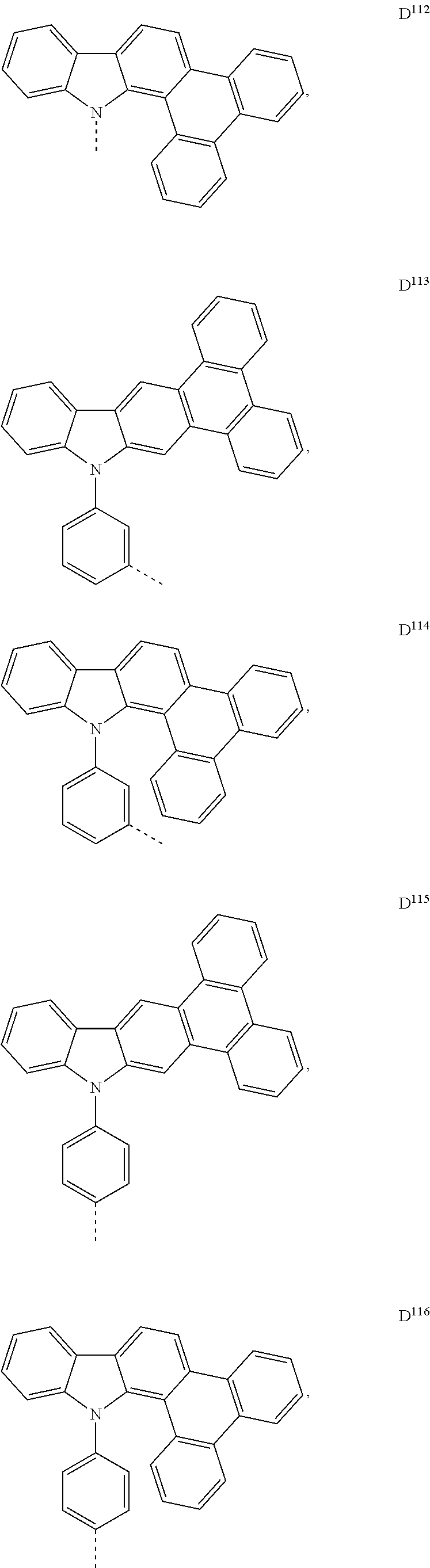


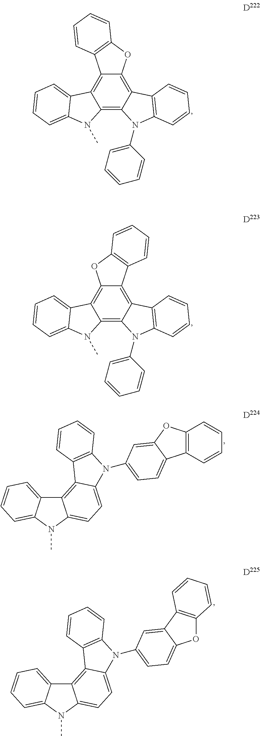


- In some embodiments, the compound is Compound x(Label) having the formula AiDj; wherein x=144j+i−144, where i is an integer from 1 to 144, and j is an integer from 1 to 244; and wherein Label is the name of X atom in the corresponding N.
- According to another aspect of the present disclosure, a first organic light emitting device comprising: an anode; a cathode; and an organic layer disposed between the anode and the cathode is disclosed. The organic layer comprises a compound having a formula selected from the group consisting of:
-

- wherein X is selected from the group consisting of O, S, and Se; wherein X1 to X10 are each independently selected from the group consisting of carbon and nitrogen; wherein at least one of X1 to X6 is nitrogen; wherein R and R′ each independently represent from mono to the possible maximum number of substitutions, or no substitution; wherein R and R′ are each independently selected from the group consisting of hydrogen, deuterium, halogen, alkyl, cycloalkyl, heteroalkyl, arylalkyl, alkoxy, aryloxy, amino, silyl, alkenyl, cycloalkenyl, heteroalkenyl, alkynyl, aryl, heteroaryl, acyl, carbonyl, carboxylic acid, ester, nitrile, isonitrile, sulfanyl, sulfinyl, sulfonyl, phosphino, and combinations thereof; wherein any adjacent substitutions on the same ring are optionally joined or fused into a ring; and
- wherein at least one of R and R′ is not hydrogen or deuterium;
- provided that when adjacent subsitutions on X5 and X6 in Formula I-1 and I-3 fuse into a six-member ring, this ring and the ring having X7 to X10 can not be pyridine at the same time.
- In some embodiments of the first organic light emitting device, the organic layer is an emissive layer and the compound is a host.
- In some embodiments of the first organic light emitting device, the organic layer further comprises a phosphorescent emissive dopant; wherein the emissive dopant is a transition metal complex having at least one ligand or part of the ligand if the ligand is more than bidentate, selected from the group consisting of:
-


- wherein each X1 to X13 are independently selected from the group consisting of carbon and nitrogen;
- wherein Z is selected from the group consisting of BR′, NR′, PR′, O, S, Se, C═O, S═O, SO2, CR′R″, SiR′R″, and GeR′R″;
- wherein R′ and R″ are optionally fused or joined to form a ring;
- wherein each Ra, Rb, Rc, and Rd may represent from mono substitution to the possible maximum number of substitution, or no substitution;
- wherein R′, R″, Ra, Rb, Rc, and Rd are each independently selected from the group consisting of hydrogen, deuterium, halogen, alkyl, cycloalkyl, heteroalkyl, arylalkyl, alkoxy, aryloxy, amino, silyl, alkenyl, cycloalkenyl, heteroalkenyl, alkynyl, aryl, heteroaryl, acyl, carbonyl, carboxylic acids, ester, nitrile, isonitrile, sulfanyl, sulfinyl, sulfonyl, phosphino, and combinations thereof; and
- wherein any two adjacent substitutents of Ra, Rb, Rc, and Rd are optionally fused or joined to form a ring or form a multidentate ligand.
- In some embodiments of the first organic light emitting device, the organic layer is a charge carrier blocking layer and the compound is a charge carrier blocking material in the organic layer.
- In some embodiments of the first organic light emitting device, the organic layer is a charge carrier transporting layer and the compound is a charge carrier transporting material in the organic layer.
- In some embodiments of the first organic light emitting device, the device can be incorporated into a consumer product, an electronic component module, an organic light-emitting device, or a lighting panel.
- In some embodiments of the first organic light emitting device, the organic layer is an emissive layer and the compound is an emitter.
- In some embodiments of the first organic light emitting device where the compound is an emitter in the emissive layer, the first organic light emitting device emits a luminescent radiation at room temperature when a voltage is applied across the first organic light emitting device, and the luminescent radiation comprises a delayed fluorescence process.
- In some embodiments of the first organic light emitting device where the compound is an emitter in the emissive layer, the emissive layer further comprises a host material.
- In some embodiments of the first organic light emitting device where the compound is an emitter in the emissive layer, the emissive layer further comprises a first phosphorescent emitting material. In some embodiments, the emissive layer further comprises a second phosphorescent emitting material.
- In some embodiments where the compound is an emitter in the emissive layer and the emissive layer further comprises a first phosphorescent emitting material, the first organic light emitting device emits a white light at room temperature when a voltage is applied across the organic light emitting device. In some embodiments of the white light emitting device, the compound emits a blue light with a peak wavelength of about 400 nm to about 500 nm. In some embodiments of the white light emitting device, the compound emits a yellow light with a peak wavelength of about 530 nm to about 580 nm.
- In another aspect of the present disclosure, a formulation comprising a compound having a formula selected from the group consisting of:
-

- is disclosed. In Formula 1-1, Formula 1-2, and Formula 1-3,
- X is selected from the group consisting of O, S, and Se;
- wherein X1 to X10 are each independently selected from the group consisting of carbon and nitrogen;
- wherein at least one of X1 to X6 is nitrogen;
- wherein R and R′ each independently represent from mono to the possible maximum number of substitutions, or no substitution;
- wherein R and R′ are each independently selected from the group consisting of hydrogen, deuterium, halogen, alkyl, cycloalkyl, heteroalkyl, arylalkyl, alkoxy, aryloxy, amino, silyl, alkenyl, cycloalkenyl, heteroalkenyl, alkynyl, aryl, heteroaryl, acyl, carbonyl, carboxylic acid, ester, nitrile, isonitrile, sulfanyl, sulfinyl, sulfonyl, phosphino, and combinations thereof;
- wherein any adjacent substitutions on the same ring are optionally joined or fused into a ring; and
- wherein at least one of R and R′ is not hydrogen or deuterium;
- provided that when adjacent subsitutions on X5 and X6 in Formula I-1 and I-3 fuse into a six-member ring, this ring and the ring having X7 to X10 can not be pyridine at the same time.
- In yet another aspect of the present disclsoure, a formulation that comprises the first compound of the present disclosure is described. The formulation can include one or more components selected from the group consisting of a solvent, a host, a hole injection material, hole transport material, and an electron transport layer material, disclosed herein.
- Combination with Other Materials
- The materials described herein as useful for a particular layer in an organic light emitting device may be used in combination with a wide variety of other materials present in the device. For example, emissive dopants disclosed herein may be used in conjunction with a wide variety of hosts, transport layers, blocking layers, injection layers, electrodes and other layers that may be present. The materials described or referred to below are non-limiting examples of materials that may be useful in combination with the compounds disclosed herein, and one of skill in the art can readily consult the literature to identify other materials that may be useful in combination.
- A charge transport layer can be doped with conductivity dopants to substantially alter its density of charge carriers, which will in turn alter its conductivity. The conductivity is increased by generating charge carriers in the matrix material, and depending on the type of dopant, a change in the Fermi level of the semiconductor may also be achieved. Hole-transporting layer can be doped by p-type conductivity dopants and n-type conductivity dopants are used in the electron-transporting layer.
- Non-limiting examples of the conductivity dopants that may be used in an OLED in combination with materials disclosed herein are exemplified below together with references that disclose those materials: EP01617493, EP01968131, EP2020694, EP2684932, US20050139810, US20070160905, US20090167167, US2010288362, WO06081780, WO2009003455, WO2009008277, WO2009011327, WO2014009310, US2007252140, US2015060804 and US2012146012.
-


- A hole injecting/transporting material to be used in the present invention is not particularly limited, and any compound may be used as long as the compound is typically used as a hole injecting/transporting material. Examples of the material include, but are not limited to: a phthalocyanine or porphyrin derivative; an aromatic amine derivative; an indolocarbazole derivative; a polymer containing fluorohydrocarbon; a polymer with conductivity dopants; a conducting polymer, such as PEDOT/PSS; a self-assembly monomer derived from compounds such as phosphonic acid and silane derivatives; a metal oxide derivative, such as MoOx; a p-type semiconducting organic compound, such as 1,4,5,8,9,12-Hexaazatriphenylenehexacarbonitrile; a metal complex, and a cross-linkable compounds.
- Examples of aromatic amine derivatives used in HIL or HTL include, but are not limited to the following general structures:
-

- Each of Ar1 to Ar9 is selected from the group consisting of aromatic hydrocarbon cyclic compounds such as benzene, biphenyl, triphenyl, triphenylene, naphthalene, anthracene, phenalene, phenanthrene, fluorene, pyrene, chrysene, perylene, and azulene; the group consisting of aromatic heterocyclic compounds such as dibenzothiophene, dibenzofuran, dibenzoselenophene, furan, thiophene, benzofuran, benzothiophene, benzoselenophene, carbazole, indolocarbazole, pyridylindole, pyrrolodipyridine, pyrazole, imidazole, triazole, oxazole, thiazole, oxadiazole, oxatriazole, dioxazole, thiadiazole, pyridine, pyridazine, pyrimidine, pyrazine, triazine, oxazine, oxathiazine, oxadiazine, indole, benzimidazole, indazole, indoxazine, benzoxazole, benzisoxazole, benzothiazole, quinoline, isoquinoline, cinnoline, quinazoline, quinoxaline, naphthyridine, phthalazine, pteridine, xanthene, acridine, phenazine, phenothiazine, phenoxazine, benzofuropyridine, furodipyridine, benzothienopyridine, thienodipyridine, benzoselenophenopyridine, and selenophenodipyridine; and the group consisting of 2 to 10 cyclic structural units which are groups of the same type or different types selected from the aromatic hydrocarbon cyclic group and the aromatic heterocyclic group and are bonded to each other directly or via at least one of oxygen atom, nitrogen atom, sulfur atom, silicon atom, phosphorus atom, boron atom, chain structural unit and the aliphatic cyclic group. Each Ar may be unsubstituted or may be substituted by a substituent selected from the group consisting of deuterium, halide, alkyl, cycloalkyl, heteroalkyl, arylalkyl, alkoxy, aryloxy, amino, silyl, alkenyl, cycloalkenyl, heteroalkenyl, alkynyl, aryl, heteroaryl, acyl, carbonyl, carboxylic acids, ester, nitrile, isonitrile, sulfanyl, sulfinyl, sulfonyl, phosphino, and combinations thereof
- In one aspect, Ar1 to Ar9 is independently selected from the group consisting of:
-

- wherein k is an integer from 1 to 20; X101 to X108 is C (including CH) or N; Z101 is NAr1, O, or S; Ar1 has the same group defined above.
- Examples of metal complexes used in HIL or HTL include, but are not limited to the following general formula:
-

- wherein Met is a metal, which can have an atomic weight greater than 40; (Y101-Y102) is a bidentate ligand, Y101 and Y102 are independently selected from C, N, O, P, and S; L101 is an ancillary ligand; k′ is an integer value from 1 to the maximum number of ligands that may be attached to the metal; and k′+k″ is the maximum number of ligands that may be attached to the metal.
- In one aspect, (Y101-Y102) is a 2-phenylpyridine derivative. In another aspect, (Y101-Y102) is a carbene ligand. In another aspect, Met is selected from Ir, Pt, Os, and Zn. In a further aspect, the metal complex has a smallest oxidation potential in solution vs. Fc+/Fc couple less than about 0.6 V.
- Non-limiting examples of the HIL and HTL materials that may be used in an OLED in combination with materials disclosed herein are exemplified below together with references that disclose those materials: CN102702075, DE102012005215, EP01624500, EP01698613, EP01806334, EP01930964, EP01972613, EP01997799, EP02011790, EP02055700, EP02055701, EP1725079, EP2085382, EP2660300, EP650955, JP07-073529, JP2005112765, JP2007091719, JP2008021687, JP2014-009196, KR20110088898, KR20130077473, TW201139402, U.S. Ser. No. 06/517,957, US20020158242, US20030162053, US20050123751, US20060182993, US20060240279, US20070145888, US20070181874, US20070278938, US20080014464, US20080091025, US20080106190, US20080124572, US20080145707, US20080220265, US20080233434, US20080303417, US2008107919, US20090115320, US20090167161, US2009066235, US2011007385, US20110163302, US2011240968, US2011278551, US2012205642, US2013241401, US20140117329, US2014183517, U.S. Pat. No. 5,061,569, U.S. Pat. No. 5,639,914, WO05075451, WO07125714, WO08023550, WO08023759, WO2009145016, WO2010061824, WO2011075644, WO2012177006, WO2013018530, WO2013039073, WO2013087142, WO2013118812, WO2013120577, WO2013157367, WO2013175747, WO2014002873, WO2014015935, WO2014015937, WO2014030872, WO2014030921, WO2014034791, WO2014104514, WO2014157018,
-


- An electron blocking layer (EBL) may be used to reduce the number of electrons and/or excitons that leave the emissive layer. The presence of such a blocking layer in a device may result in substantially higher efficiencies, and or longer lifetime, as compared to a similar device lacking a blocking layer. Also, a blocking layer may be used to confine emission to a desired region of an OLED. In some embodiments, the EBL material has a higher LUMO (closer to the vacuum level) and/or higher triplet energy than the emitter closest to the EBL interface. In some embodiments, the EBL material has a higher LUMO (closer to the vacuum level) and or higher triplet energy than one or more of the hosts closest to the EBL interface. In one aspect, the compound used in EBL contains the same molecule or the same functional groups used as one of the hosts described below.
- The light emitting layer of the organic EL device of the present invention preferably contains at least a metal complex as light emitting dopant material, and may contain one or more additional host materials using the metal complex as a dopant material. Examples of the host material are not particularly limited, and any metal complexes or organic compounds may be used as long as the triplet energy of the host is larger than that of the dopant. Any host material may be used with any dopant so long as the triplet criteria is satisfied.
- Examples of metal complexes used as host are preferred to have the following general formula:
-

- wherein Met is a metal; (Y103-Y104) is a bidentate ligand, Y103 and Y104 are independently selected from C, N, O, P, and S; L101 is an another ligand; k′ is an integer value from 1 to the maximum number of ligands that may be attached to the metal; and k′+k″ is the maximum number of ligands that may be attached to the metal.
- In one aspect, the metal complexes are:
-

- wherein (O—N) is a bidentate ligand, having metal coordinated to atoms O and N.
- In another aspect, Met is selected from Ir and Pt. In a further aspect, (Y103-Y104) is a carbene ligand.
- Examples of other organic compounds used as additional host are selected from the group consisting of aromatic hydrocarbon cyclic compounds such as benzene, biphenyl, triphenyl, triphenylene, naphthalene, anthracene, phenalene, phenanthrene, fluorene, pyrene, chrysene, perylene, azulene; group consisting aromatic heterocyclic compounds such as dibenzothiophene, dibenzofuran, dibenzoselenophene, furan, thiophene, benzofuran, benzothiophene, benzoselenophene, carbazole, indolocarbazole, pyridylindole, pyrrolodipyridine, pyrazole, imidazole, triazole, oxazole, thiazole, oxadiazole, oxatriazole, dioxazole, thiadiazole, pyridine, pyridazine, pyrimidine, pyrazine, triazine, oxazine, oxathiazine, oxadiazine, indole, benzimidazole, indazole, indoxazine, benzoxazole, benzisoxazole, benzothiazole, quinoline, isoquinoline, cinnoline, quinazoline, quinoxaline, naphthyridine, phthalazine, pteridine, xanthene, acridine, phenazine, phenothiazine, phenoxazine, benzofuropyridine, furodipyridine, benzothienopyridine, thienodipyridine, benzoselenophenopyridine, and selenophenodipyridine; and group consisting 2 to 10 cyclic structural units which are groups of the same type or different types selected from the aromatic hydrocarbon cyclic group and the aromatic heterocyclic group and are bonded to each other directly or via at least one of oxygen atom, nitrogen atom, sulfur atom, silicon atom, phosphorus atom, boron atom, chain structural unit and the aliphatic cyclic group. Wherein each group is further substituted by a substituent selected from the group consisting of hydrogen, deuterium, halide, alkyl, cycloalkyl, heteroalkyl, arylalkyl, alkoxy, aryloxy, amino, silyl, alkenyl, cycloalkenyl, heteroalkenyl, alkynyl, aryl, heteroaryl, acyl, carbonyl, carboxylic acids, ester, nitrile, isonitrile, sulfanyl, sulfinyl, sulfonyl, phosphino, and combinations thereof.
- In one aspect, host compound contains at least one of the following groups in the molecule:
-


- wherein R101 to R107 is independently selected from the group consisting of hydrogen, deuterium, halide, alkyl, cycloalkyl, heteroalkyl, arylalkyl, alkoxy, aryloxy, amino, silyl, alkenyl, cycloalkenyl, heteroalkenyl, alkynyl, aryl, heteroaryl, acyl, carbonyl, carboxylic acids, ester, nitrile, isonitrile, sulfanyl, sulfinyl, sulfonyl, phosphino, and combinations thereof, when it is aryl or heteroaryl, it has the similar definition as Ar's mentioned above. k is an integer from 0 to 20 or 1 to 20; k′″ is an integer from 0 to 20. X101 to X108 is selected from C (including CH) or N.
- Z101 and L102 is selected from NR101, O, or S.
- Non-limiting examples of the additional host materials that may be used in an OLED in combination with the host compound disclosed herein are exemplified below together with references that disclose those materials: EP2034538, EP2034538A, EP2757608, JP2007254297, KR20100079458, KR20120088644, KR20120129733, KR20130115564, TW201329200, US20030175553, US20050238919, US20060280965, US20090017330, US20090030202, US20090167162, US20090302743, US20090309488, US20100012931, US20100084966, US20100187984, US2010187984, US2012075273, US2012126221, US2013009543, US2013105787, US2013175519, US2014001446, US20140183503, US20140225088, US2014034914, U.S. Pat. No. 7,154,114, WO2001039234, WO2004093207, WO2005014551, WO2005089025, WO2006072002, WO2006114966, WO2007063754, WO2008056746, WO2009003898, WO2009021126, WO2009063833, WO2009066778, WO2009066779, WO2009086028, WO2010056066, WO2010107244, WO2011081423, WO02011081431, WO2011086863, WO2012128298, WO2012133644, WO2012133649, WO2013024872, WO2013035275, WO2013081315, WO2013191404, WO2014142472,
-


- An emitter example is not particularly limited, and any compound may be used as long as the compound is typically used as an emitter material. Examples of suitable emitter materials include, but are not limited to, compounds which can produce emissions via phosphorescence, fluorescence, thermally activated delayed fluorescence, i.e., TADF (also referred to as E-type delayed fluorescence), triplet-triplet annihilation, or combinations of these processes.
- Non-limiting examples of the emitter materials that may be used in an OLED in combination with materials disclosed herein are exemplified below together with references that disclose those materials: CN103694277, CN1696137, EB01238981, EP01239526, EP01961743, EP1239526, EP1244155, EP1642951, EP1647554, EP1841834, EP1841834B, EP2062907, EP2730583, JP2012074444, JP2013110263, JP4478555, KR1020090133652, KR20120032054, KR20130043460, TW201332980, U.S. Ser. No. 06/699,599, U.S. Ser. No. 06/916,554, US20010019782, US20020034656, US20030068526, US20030072964, US20030138657, US20050123788, US20050244673, US2005123791, US2005260449, US20060008670, US20060065890, US20060127696, US20060134459, US20060134462, US20060202194, US20060251923, US20070034863, US20070087321, US20070103060, US20070111026, US20070190359, US20070231600, US2007034863, US2007104979, US2007104980, US2007138437, US2007224450, US2007278936, US20080020237, US20080233410, US20080261076, US20080297033, US200805851, US2008161567, US2008210930, US20090039776, US20090108737, US20090115322, US20090179555, US2009085476, US2009104472, US20100090591, US20100148663, US20100244004, US20100295032, US2010102716, US2010105902, US2010244004, US2010270916, US20110057559, US20110108822, US20110204333, US2011215710, US2011227049, US2011285275, US2012292601, US20130146848, US2013033172, US2013165653, US2013181190, US2013334521, US20140246656, US2014103305, U.S. Pat. No. 6,303,238, U.S. Pat. No. 6,413,656, U.S. Pat. No. 6,653,654, U.S. Pat. No. 6,670,645, U.S. Pat. No. 6,687,266, U.S. Pat. No. 6,835,469, U.S. Pat. No. 6,921,915, U.S. Pat. No. 7,279,704, U.S. Pat. No. 7,332,232, U.S. Pat. No. 7,378,162, U.S. Pat. No. 7,534,505, U.S. Pat. No. 7,675,228, U.S. Pat. No. 7,728,137, U.S. Pat. No. 7,740,957, U.S. Pat. No. 7,759,489, U.S. Pat. No. 7,951,947, U.S. Pat. No. 8,067,099, U.S. Pat. No. 8,592,586, U.S. Pat. No. 8,871,361, WO06081973, WO06121811, WO07018067, WO07108362, WO07115970, WO07115981, WO08035571, WO2002015645, WO2003040257, WO2005019373, WO2006056418, WO2008054584, WO2008078800, WO2008096609, WO2008101842, WO2009000673, WO2009050281, WO2009100991, WO2010028151, WO2010054731, WO2010086089, WO2010118029, WO2011044988, WO2011051404, WO2011107491, WO2012020327, WO2012163471, WO2013094620, WO2013107487, WO2013174471, WO2014007565, WO2014008982, WO2014023377, WO2014024131, WO2014031977, WO2014038456, WO2014112450,
-


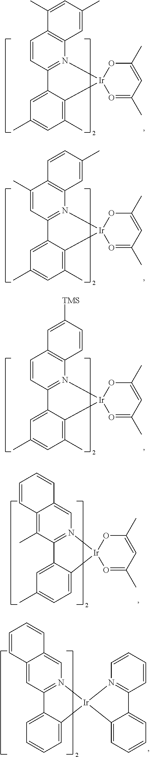


- A hole blocking layer (HBL) may be used to reduce the number of holes and/or excitons that leave the emissive layer. The presence of such a blocking layer in a device may result in substantially higher efficiencies and/or longer lifetime as compared to a similar device lacking a blocking layer. Also, a blocking layer may be used to confine emission to a desired region of an OLED. In some embodiments, the HBL material has a lower HOMO (further from the vacuum level) and or higher triplet energy than the emitter closest to the HBL interface. In some embodiments, the HBL material has a lower HOMO (further from the vacuum level) and or higher triplet energy than one or more of the hosts closest to the HBL interface.
- In one aspect, compound used in HBL contains the same molecule or the same functional groups used as host described above.
- In another aspect, compound used in HBL contains at least one of the following groups in the molecule:
-

- wherein k is an integer from 1 to 20; L101 is an another ligand, k′ is an integer from 1 to 3.
- Electron transport layer (ETL) may include a material capable of transporting electrons. Electron transport layer may be intrinsic (undoped), or doped. Doping may be used to enhance conductivity. Examples of the ETL material are not particularly limited, and any metal complexes or organic compounds may be used as long as they are typically used to transport electrons.
- In one aspect, compound used in ETL contains at least one of the following groups in the molecule:
-

- wherein R101 is selected from the group consisting of hydrogen, deuterium, halide, alkyl, cycloalkyl, heteroalkyl, arylalkyl, alkoxy, aryloxy, amino, silyl, alkenyl, cycloalkenyl, heteroalkenyl, alkynyl, aryl, heteroaryl, acyl, carbonyl, carboxylic acids, ester, nitrile, isonitrile, sulfanyl, sulfinyl, sulfonyl, phosphino, and combinations thereof, when it is aryl or heteroaryl, it has the similar definition as Ar's mentioned above. Ar1 to Ar3 has the similar definition as Ar's mentioned above. k is an integer from 1 to 20. X101 to X108 is selected from C (including CH) or N.
- In another aspect, the metal complexes used in ETL include, but are not limited to the following general formula:
-

- wherein (O—N) or (N—N) is a bidentate ligand, having metal coordinated to atoms O, N or N, N; L101 is another ligand; k′ is an integer value from 1 to the maximum number of ligands that may be attached to the metal.
- Non-limiting examples of the ETL materials that may be used in an OLED in combination with materials disclosed herein are exemplified below together with references that disclose those materials: CN103508940, EP01602648, EP01734038, EP01956007, JP2004-022334, JP2005149918, JP2005-268199, KR0117693, KR20130108183, US20040036077, US20070104977, US2007018155, US20090101870, US20090115316, US20090140637, US20090179554, US2009218940, US2010108990, US2011156017, US2011210320, US2012193612, US2012214993, US2014014925, US2014014927, US20140284580, U.S. Pat. No. 6,656,612, U.S. Pat. No. 8,415,031, WO2003060956, WO2007111263, WO2009148269, WO2010067894, WO2010072300, WO2011074770, WO2011105373, WO2013079217, WO2013145667, WO2013180376, WO2014104499, WO2014104535,
-


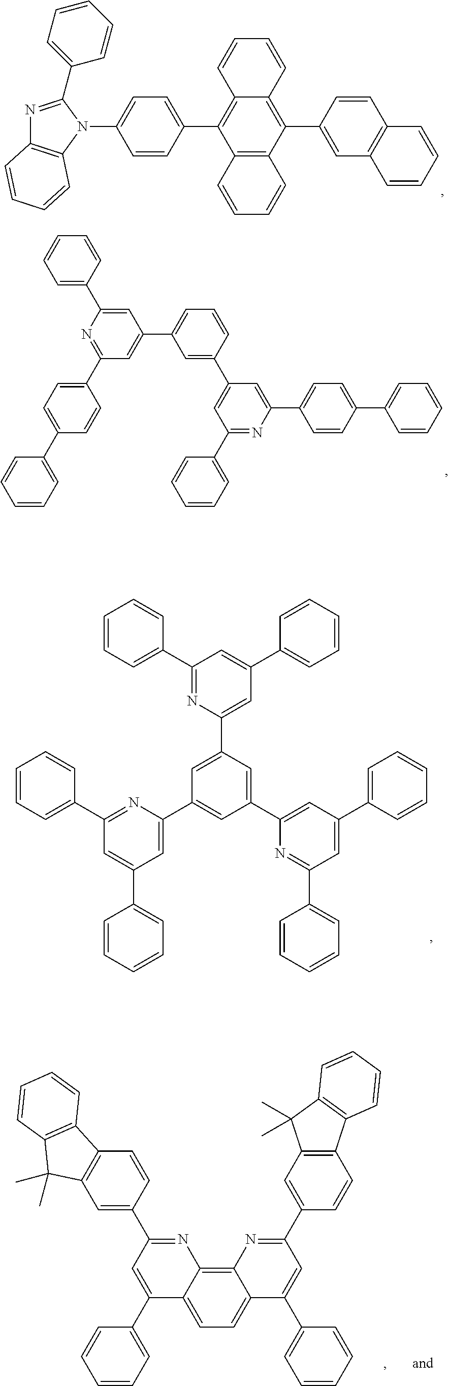

- In tandem or stacked OLEDs, the CGL plays an essential role in the performance, which is composed of an n-doped layer and a p-doped layer for injection of electrons and holes, respectively. Electrons and holes are supplied from the CGL and electrodes. The consumed electrons and holes in the CGL are refilled by the electrons and holes injected from the cathode and anode, respectively; then, the bipolar currents reach a steady state gradually. Typical CGL materials include n and p conductivity dopants used in the transport layers.
- In any above-mentioned compounds used in each layer of the OLED device, the hydrogen atoms can be partially or fully deuterated. Thus, any specifically listed substituent, such as, without limitation, methyl, phenyl, pyridyl, etc. encompasses undeuterated, partially deuterated, and fully deuterated versions thereof Similarly, classes of substituents such as, without limitation, alkyl, aryl, cycloalkyl, heteroaryl, etc. also encompass undeuterated, partially deuterated, and fully deuterated versions thereof
- Chemical abbreviations used throughout this document are as follows: Pd2(dba)3 is tri(dibenzylideneacetone) dipalladium(0); SPhos is dicyclohexyl(2′,6′-dimethoxy-[1,1′-biphenyl]-2-yl)phosphine; and DCM is dichloromethane.
- Synthesis of Compound 9073(S)
-

- A solution of 9-phenyl-9H,9′H-3,3′-bicarbazole (3.5 g, 8.57 mmol), 6-chlorobenzo[4,5]thieno[2,3-c]quinoline (3.47 g, 12.85 mmol), sodium tert-butoxide (2.059 g, 21.42 mmol) in o-xylene (200 ml) was degassed for 20 mins. Pd2(dba)3 (0.392 g, 0.428 mmol), SPhos (0.352 g, 0.857 mmol) were added. The mixture was heated to reflux under nitrogen for 16 hours. After cooling to room temperature, the solid was removed by filtration and the solvent was evaporated. The residue was purified by column chromatography on silica gel with heptane/DCM (7/3 to 6/4, v/v) as eluent and recrystallization from heptane to yield Compound 9073(S) (4.0 g, 73%) as a yellow solid.
- Synthesis of Compound 9195(S)
-

- A solution of 9-phenyl-9H,9′H-3,3′-bicarbazole (3.15 g, 7.71 mmol), 6-chlorodibenzo[f,h]benzo[4,5]thieno[2,3-c]quinoline (3.42 g, 9.25 mmol), Pd2(dba)3 (0.282 g, 0.308 mmol), SPhos (0.8 g, 1.951 mmol) and sodium tert-butoxide (1.703 g, 17.74 mmol), in o-xylene (200 ml) was degased and refluxed under nitrogen for 24 hours. After cooling to room temperature, the solid was removed by filtration and the solvent was evaporated. The residue was purified by column chromatography on silica gel with heptane/DCM (7/3 to 1/99, v/v) as eluent and trituration with ethanol to yield Compound 9195(S) as a yellow solid.
- Synthesis of Compound 20737(S)
-

- A solution of 6-chlorobenzo[4,5]thieno[2,3-c]quinoline (2.87 g, 10.65 mmol) and 5-([1,1′-biphenyl]-4-yl)-5,8-dihydroindolo[2,3-c]carbazole (2.9 g, 7.10 mmol), sodium tert-butoxide (1.706 g, 17.75 mmol) in o-xylene (20 ml) was degassed for 20 mins. Pd2(dba)3 (0.325 g, 0.355 mmol), SPhos (0.291 g, 0.710 mmol) were added. The mixture was heated to reflux under nitrogen for 3 h. After coling to room temperature, the reaction mixture was filtered through a short plug of silica gel. Upon evaporation off the solvent, the residue was triturated successively with ethanol, ethyl acetate, toluene, DCM and toluene to yield Compound 20737(S) (2.3 g, 50%) as a yellow solid.
- Application in OLED: All devices were fabricated by high vacuum (˜10−7 Torr) thermal evaporation. The anode electrode was 120 nm of indium tin oxide (ITO). The cathode electrode consisted of 1 nm of LiF followed by 100 nm of Al. All devices were encapsulated with a glass lid sealed with an epoxy resin in a nitrogen glove box (<1 ppm of H2O and O2) immediately after fabrication, and a moisture getter was incorporated inside the package.
- Device Examples: A first set of device examples have organic stacks consisting of, sequentially, from the ITO surface, 10 nm of LG101 (from LG Chem) as the hole injection layer (HIL), 40 nm of PPh-TPD as the hole-transport layer (HTL), 40 nm of emissive layer (EML), followed by 35 nm of aDBT-ADN with LiQ as the electron-transport layer (ETL). The EML has two components, 97 wt % of invented compounds (Compounds 9073(S), or 20737(S)) or comparative compounds (CC-1, CC-2 or CC-3) as the host, and 3 wt % of RD as the emitter. The structure of the compounds used are shown below:
-


- Table D1, below, is a summary of the device data, emission color and external quantum efficiency (EQE). recorded at 1000 nits for the devices.
-
Emission EQE Device ID Host Color [%] Device-1 Compound 9073(S) Red 24.4 Device-2 Compound 20737(S) Red 23.9 Device-C1 CC-1 Red 10.2 Device-C2 CC-2 Red 11.6 Device-C3 CC-3 Red 21.2 - The data in Table D1 shows that OLEDs (Device-1 and Device-2) using inventive compounds as the host in the EML are much more efficient than their conterparts using comparative compounds (CC-1, CC-2 and CC-3) as the host. The superior performance of the inventice compounds are attributable to their unique chemical structures containing benzo-fused aza-dibenzothiophene that might have facilitated charge transport to achieve a more balanced charge carrier fluxes inside the devices, which is critical to enhance OLED device performance.
- It is understood that the various embodiments described herein are by way of example only, and are not intended to limit the scope of the invention. For example, many of the materials and structures described herein may be substituted with other materials and structures without deviating from the spirit of the invention. The present invention as claimed may therefore include variations from the particular examples and preferred embodiments described herein, as will be apparent to one of skill in the art. It is understood that various theories as to why the invention works are not intended to be limiting.
Claims (26)


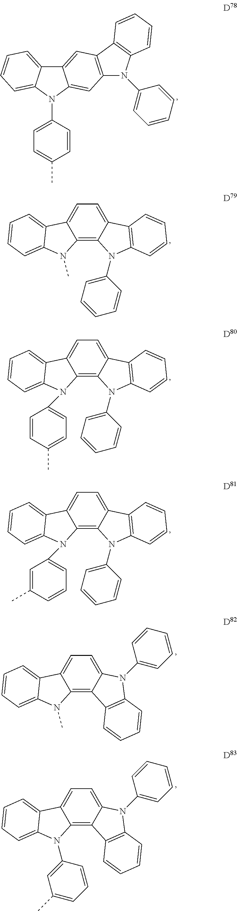


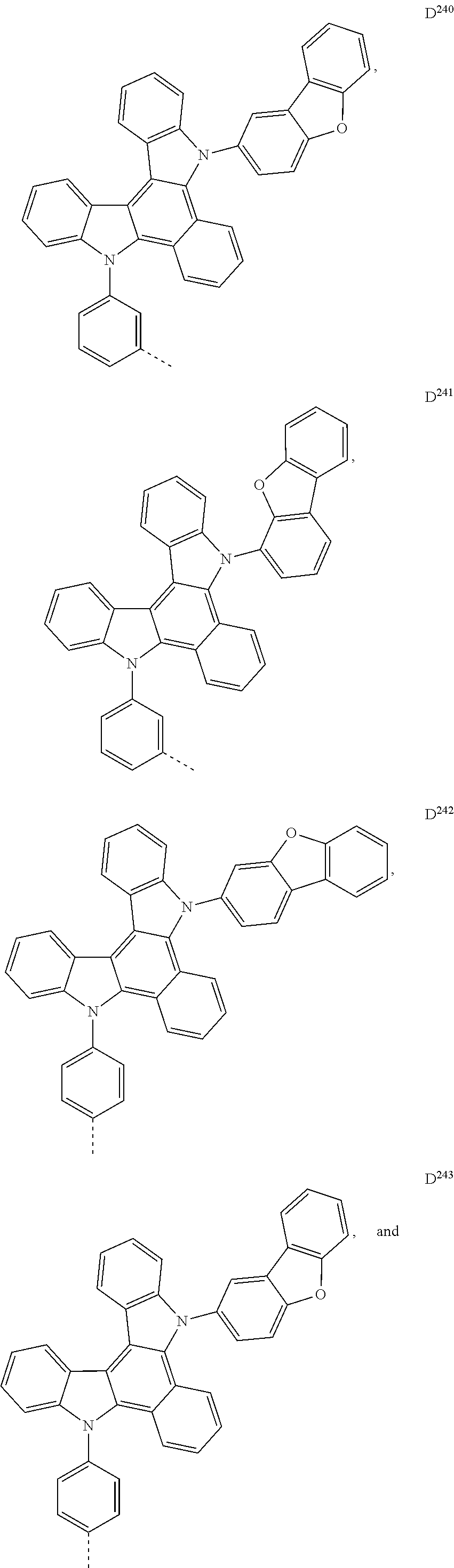


Priority Applications (8)
| Application Number | Priority Date | Filing Date | Title |
|---|---|---|---|
| US15/173,806 US11127905B2 (en) | 2015-07-29 | 2016-06-06 | Organic electroluminescent materials and devices |
| JP2016133931A JP6850086B2 (en) | 2015-07-29 | 2016-07-06 | Organic electroluminescence materials and devices |
| EP16179494.6A EP3124488B1 (en) | 2015-07-29 | 2016-07-14 | Organic electroluminescent materials and devices |
| CN201610604947.2A CN106397460B (en) | 2015-07-29 | 2016-07-28 | Organic electroluminescent material and device |
| CN202011493160.6A CN112521399B (en) | 2015-07-29 | 2016-07-28 | Organic electroluminescent material and device |
| KR1020160096065A KR102604511B1 (en) | 2015-07-29 | 2016-07-28 | Organic electroluminescent materials and devices |
| US17/397,373 US20210376256A1 (en) | 2015-07-29 | 2021-08-09 | Organic electroluminescent materials and devices |
| KR1020230158524A KR20230161915A (en) | 2015-07-29 | 2023-11-15 | Organic electroluminescent materials and devices |
Applications Claiming Priority (2)
| Application Number | Priority Date | Filing Date | Title |
|---|---|---|---|
| US201562198173P | 2015-07-29 | 2015-07-29 | |
| US15/173,806 US11127905B2 (en) | 2015-07-29 | 2016-06-06 | Organic electroluminescent materials and devices |
Related Child Applications (1)
| Application Number | Title | Priority Date | Filing Date |
|---|---|---|---|
| US17/397,373 Continuation US20210376256A1 (en) | 2015-07-29 | 2021-08-09 | Organic electroluminescent materials and devices |
Publications (2)
| Publication Number | Publication Date |
|---|---|
| US20170033295A1 true US20170033295A1 (en) | 2017-02-02 |
| US11127905B2 US11127905B2 (en) | 2021-09-21 |
Family
ID=56411546
Family Applications (2)
| Application Number | Title | Priority Date | Filing Date |
|---|---|---|---|
| US15/173,806 Active 2037-09-15 US11127905B2 (en) | 2015-07-29 | 2016-06-06 | Organic electroluminescent materials and devices |
| US17/397,373 Pending US20210376256A1 (en) | 2015-07-29 | 2021-08-09 | Organic electroluminescent materials and devices |
Family Applications After (1)
| Application Number | Title | Priority Date | Filing Date |
|---|---|---|---|
| US17/397,373 Pending US20210376256A1 (en) | 2015-07-29 | 2021-08-09 | Organic electroluminescent materials and devices |
Country Status (5)
| Country | Link |
|---|---|
| US (2) | US11127905B2 (en) |
| EP (1) | EP3124488B1 (en) |
| JP (1) | JP6850086B2 (en) |
| KR (2) | KR102604511B1 (en) |
| CN (2) | CN112521399B (en) |
Cited By (5)
| Publication number | Priority date | Publication date | Assignee | Title |
|---|---|---|---|---|
| WO2019063288A1 (en) * | 2017-09-26 | 2019-04-04 | Cynora Gmbh | Organic molecules, in particular for use in optoelctronic devices |
| CN111051471A (en) * | 2017-09-01 | 2020-04-21 | 九州有机光材股份有限公司 | Composition for use in organic light emitting diodes |
| US11476425B2 (en) | 2018-09-28 | 2022-10-18 | Lt Materials Co., Ltd. | Heterocyclic compound and organic light emitting element comprising same |
| US11495753B2 (en) * | 2017-03-16 | 2022-11-08 | Semiconductor Energy Laboratory Co., Ltd. | Organic compound, light-emitting element, light-emitting device, electronic device, and lighting device |
| US11691983B2 (en) * | 2016-06-22 | 2023-07-04 | Idemitsu Kosan Co., Ltd. | Specifically substituted benzofuro- and benzothienoquinolines for organic light emitting diodes |
Families Citing this family (11)
| Publication number | Priority date | Publication date | Assignee | Title |
|---|---|---|---|---|
| US20190031673A1 (en) * | 2017-07-27 | 2019-01-31 | Semiconductor Energy Laboratory Co., Ltd. | Organic Compound, Light-Emitting Element, Light-Emitting Device, Electronic Device, and Lighting Device |
| JP7198804B2 (en) * | 2018-03-16 | 2023-01-11 | 日鉄ケミカル&マテリアル株式会社 | organic electroluminescent device |
| KR102154948B1 (en) * | 2018-06-28 | 2020-09-10 | 에스케이머티리얼즈 주식회사 | Compound, organic electroluminescent device and display device |
| WO2020067595A1 (en) * | 2018-09-28 | 2020-04-02 | 희성소재(주) | Heterocyclic compound and organic light emitting diode comprising same |
| TWI795444B (en) * | 2018-10-01 | 2023-03-11 | 南韓商Lt素材股份有限公司 | Heterocyclic compound and organic light emitting device comprising the same |
| CN109678876A (en) * | 2018-11-08 | 2019-04-26 | 浙江华显光电科技有限公司 | A kind of red phosphorescent compound and its organic luminescent device using the compound |
| CN109678868A (en) * | 2018-11-08 | 2019-04-26 | 浙江华显光电科技有限公司 | A kind of red phosphorescent compound and its organic luminescent device using the compound |
| KR102177586B1 (en) * | 2018-11-26 | 2020-11-11 | 엘티소재주식회사 | Heterocyclic compound and organic light emitting device comprising the same |
| CN109503607A (en) * | 2018-11-26 | 2019-03-22 | 浙江华显光电科技有限公司 | A kind of phosphorescence host compound and its organic electroluminescence device using the compound |
| KR102211131B1 (en) * | 2019-01-25 | 2021-02-03 | 엘티소재주식회사 | Compound, composition and organic optoelectronic device and display device |
| WO2023085789A1 (en) * | 2021-11-10 | 2023-05-19 | 주식회사 엘지화학 | Novel compound and organic light-emitting device comprising same |
Citations (4)
| Publication number | Priority date | Publication date | Assignee | Title |
|---|---|---|---|---|
| US20100295032A1 (en) * | 2009-05-20 | 2010-11-25 | Universal Display Corporation | Metal complexes with boron-nitrogen heterocycle containing ligands |
| US20160141515A1 (en) * | 2013-06-11 | 2016-05-19 | Idemitsu Kosan Co., Ltd. | Material for organic electroluminescent elements, organic electroluminescent element using same, and electronic device |
| US20170141325A1 (en) * | 2014-06-27 | 2017-05-18 | Heesung Material Ltd. | Heterocyclic compound and organic light emitting device using same |
| US20170141331A1 (en) * | 2014-08-06 | 2017-05-18 | Samsung Sdi Co.,Ltd. | Organic compound, organic optoelectronic element, and display device |
Family Cites Families (380)
| Publication number | Priority date | Publication date | Assignee | Title |
|---|---|---|---|---|
| US4769292A (en) | 1987-03-02 | 1988-09-06 | Eastman Kodak Company | Electroluminescent device with modified thin film luminescent zone |
| GB8909011D0 (en) | 1989-04-20 | 1989-06-07 | Friend Richard H | Electroluminescent devices |
| US5061569A (en) | 1990-07-26 | 1991-10-29 | Eastman Kodak Company | Electroluminescent device with organic electroluminescent medium |
| JPH0773529A (en) | 1993-08-31 | 1995-03-17 | Hitachi Ltd | Magneto-optical recording system and magneto-optical recording medium |
| DE69412567T2 (en) | 1993-11-01 | 1999-02-04 | Hodogaya Chemical Co Ltd | Amine compound and electroluminescent device containing it |
| US5703436A (en) | 1994-12-13 | 1997-12-30 | The Trustees Of Princeton University | Transparent contacts for organic devices |
| US5707745A (en) | 1994-12-13 | 1998-01-13 | The Trustees Of Princeton University | Multicolor organic light emitting devices |
| US6939625B2 (en) | 1996-06-25 | 2005-09-06 | Nôrthwestern University | Organic light-emitting diodes and methods for assembly and enhanced charge injection |
| US5844363A (en) | 1997-01-23 | 1998-12-01 | The Trustees Of Princeton Univ. | Vacuum deposited, non-polymeric flexible organic light emitting devices |
| US6091195A (en) | 1997-02-03 | 2000-07-18 | The Trustees Of Princeton University | Displays having mesa pixel configuration |
| US5834893A (en) | 1996-12-23 | 1998-11-10 | The Trustees Of Princeton University | High efficiency organic light emitting devices with light directing structures |
| US6013982A (en) | 1996-12-23 | 2000-01-11 | The Trustees Of Princeton University | Multicolor display devices |
| US6517957B1 (en) | 1997-05-19 | 2003-02-11 | Canon Kabushiki Kaisha | Organic compound and electroluminescent device using the same |
| US6413656B1 (en) | 1998-09-14 | 2002-07-02 | The University Of Southern California | Reduced symmetry porphyrin molecules for producing enhanced luminosity from phosphorescent organic light emitting devices |
| US6303238B1 (en) | 1997-12-01 | 2001-10-16 | The Trustees Of Princeton University | OLEDs doped with phosphorescent compounds |
| US6337102B1 (en) | 1997-11-17 | 2002-01-08 | The Trustees Of Princeton University | Low pressure vapor phase deposition of organic thin films |
| US6087196A (en) | 1998-01-30 | 2000-07-11 | The Trustees Of Princeton University | Fabrication of organic semiconductor devices using ink jet printing |
| US6528187B1 (en) | 1998-09-08 | 2003-03-04 | Fuji Photo Film Co., Ltd. | Material for luminescence element and luminescence element using the same |
| US6830828B2 (en) | 1998-09-14 | 2004-12-14 | The Trustees Of Princeton University | Organometallic complexes as phosphorescent emitters in organic LEDs |
| US6097147A (en) | 1998-09-14 | 2000-08-01 | The Trustees Of Princeton University | Structure for high efficiency electroluminescent device |
| US6461747B1 (en) | 1999-07-22 | 2002-10-08 | Fuji Photo Co., Ltd. | Heterocyclic compounds, materials for light emitting devices and light emitting devices using the same |
| US6294398B1 (en) | 1999-11-23 | 2001-09-25 | The Trustees Of Princeton University | Method for patterning devices |
| US6458475B1 (en) | 1999-11-24 | 2002-10-01 | The Trustee Of Princeton University | Organic light emitting diode having a blue phosphorescent molecule as an emitter |
| US6821645B2 (en) | 1999-12-27 | 2004-11-23 | Fuji Photo Film Co., Ltd. | Light-emitting material comprising orthometalated iridium complex, light-emitting device, high efficiency red light-emitting device, and novel iridium complex |
| KR100377321B1 (en) | 1999-12-31 | 2003-03-26 | 주식회사 엘지화학 | Electronic device comprising organic compound having p-type semiconducting characteristics |
| US20020121638A1 (en) | 2000-06-30 | 2002-09-05 | Vladimir Grushin | Electroluminescent iridium compounds with fluorinated phenylpyridines, phenylpyrimidines, and phenylquinolines and devices made with such compounds |
| US6670645B2 (en) | 2000-06-30 | 2003-12-30 | E. I. Du Pont De Nemours And Company | Electroluminescent iridium compounds with fluorinated phenylpyridines, phenylpyrimidines, and phenylquinolines and devices made with such compounds |
| JP2002050860A (en) | 2000-08-04 | 2002-02-15 | Toray Eng Co Ltd | Method and device for mounting |
| CN100505375C (en) | 2000-08-11 | 2009-06-24 | 普林斯顿大学理事会 | Organometallic compounds and emission-shifting organic electrophosphorescence |
| KR100846526B1 (en) | 2000-11-30 | 2008-07-15 | 캐논 가부시끼가이샤 | Luminescent Element and Display |
| JP4154145B2 (en) | 2000-12-01 | 2008-09-24 | キヤノン株式会社 | Metal coordination compound, light emitting device and display device |
| US6579630B2 (en) | 2000-12-07 | 2003-06-17 | Canon Kabushiki Kaisha | Deuterated semiconducting organic compounds used for opto-electronic devices |
| JP3812730B2 (en) | 2001-02-01 | 2006-08-23 | 富士写真フイルム株式会社 | Transition metal complex and light emitting device |
| JP4307000B2 (en) | 2001-03-08 | 2009-08-05 | キヤノン株式会社 | Metal coordination compound, electroluminescent element and display device |
| JP4438042B2 (en) | 2001-03-08 | 2010-03-24 | キヤノン株式会社 | Metal coordination compound, electroluminescent element and display device |
| JP4307001B2 (en) | 2001-03-14 | 2009-08-05 | キヤノン株式会社 | Metal coordination compound, electroluminescent element and display device |
| DE10116962A1 (en) | 2001-04-05 | 2002-10-10 | Covion Organic Semiconductors | Rhodium and iridium complexes |
| JP4310077B2 (en) | 2001-06-19 | 2009-08-05 | キヤノン株式会社 | Metal coordination compound and organic light emitting device |
| WO2003001616A2 (en) | 2001-06-20 | 2003-01-03 | Showa Denko K.K. | Light emitting material and organic light-emitting device |
| US7071615B2 (en) | 2001-08-20 | 2006-07-04 | Universal Display Corporation | Transparent electrodes |
| US7250226B2 (en) | 2001-08-31 | 2007-07-31 | Nippon Hoso Kyokai | Phosphorescent compound, a phosphorescent composition and an organic light-emitting device |
| US7431968B1 (en) | 2001-09-04 | 2008-10-07 | The Trustees Of Princeton University | Process and apparatus for organic vapor jet deposition |
| US6835469B2 (en) | 2001-10-17 | 2004-12-28 | The University Of Southern California | Phosphorescent compounds and devices comprising the same |
| US7166368B2 (en) | 2001-11-07 | 2007-01-23 | E. I. Du Pont De Nemours And Company | Electroluminescent platinum compounds and devices made with such compounds |
| US6863997B2 (en) | 2001-12-28 | 2005-03-08 | The Trustees Of Princeton University | White light emitting OLEDs from combined monomer and aggregate emission |
| KR100691543B1 (en) | 2002-01-18 | 2007-03-09 | 주식회사 엘지화학 | New material for transporting electron and organic electroluminescent display using the same |
| US6653654B1 (en) | 2002-05-01 | 2003-11-25 | The University Of Hong Kong | Electroluminescent materials |
| JP4106974B2 (en) | 2002-06-17 | 2008-06-25 | コニカミノルタホールディングス株式会社 | Organic electroluminescence element and display device |
| US20030230980A1 (en) | 2002-06-18 | 2003-12-18 | Forrest Stephen R | Very low voltage, high efficiency phosphorescent oled in a p-i-n structure |
| US6916554B2 (en) | 2002-11-06 | 2005-07-12 | The University Of Southern California | Organic light emitting materials and devices |
| US7189989B2 (en) | 2002-08-22 | 2007-03-13 | Fuji Photo Film Co., Ltd. | Light emitting element |
| DE10238903A1 (en) | 2002-08-24 | 2004-03-04 | Covion Organic Semiconductors Gmbh | New heteroaromatic rhodium and iridium complexes, useful in electroluminescent and/or phosphorescent devices as the emission layer and for use in solar cells, photovoltaic devices and organic photodetectors |
| EP1550707B1 (en) | 2002-08-27 | 2016-03-23 | UDC Ireland Limited | Organometallic complexes, organic el devices, and organic el displays |
| JP4261855B2 (en) | 2002-09-19 | 2009-04-30 | キヤノン株式会社 | Phenanthroline compound and organic light emitting device using the same |
| US6687266B1 (en) | 2002-11-08 | 2004-02-03 | Universal Display Corporation | Organic light emitting materials and devices |
| JP4365199B2 (en) | 2002-12-27 | 2009-11-18 | 富士フイルム株式会社 | Organic electroluminescence device |
| JP4365196B2 (en) | 2002-12-27 | 2009-11-18 | 富士フイルム株式会社 | Organic electroluminescence device |
| DE10310887A1 (en) | 2003-03-11 | 2004-09-30 | Covion Organic Semiconductors Gmbh | Matallkomplexe |
| CN101503393B (en) | 2003-03-13 | 2015-08-19 | 出光兴产株式会社 | Nitrogen-containing heterocyclic derivative and organic electroluminescent element using same |
| EP3109238B1 (en) | 2003-03-24 | 2019-09-18 | University of Southern California | Phenyl-pyrazole complexes of iridium |
| US7090928B2 (en) | 2003-04-01 | 2006-08-15 | The University Of Southern California | Binuclear compounds |
| WO2004093207A2 (en) | 2003-04-15 | 2004-10-28 | Covion Organic Semiconductors Gmbh | Mixtures of matrix materials and organic semiconductors capable of emission, use of the same and electronic components containing said mixtures |
| US7029765B2 (en) | 2003-04-22 | 2006-04-18 | Universal Display Corporation | Organic light emitting devices having reduced pixel shrinkage |
| KR101032355B1 (en) | 2003-05-29 | 2011-05-03 | 신닛테츠가가쿠 가부시키가이샤 | Organic electroluminescent element |
| JP2005011610A (en) | 2003-06-18 | 2005-01-13 | Nippon Steel Chem Co Ltd | Organic electroluminescent element |
| CN1829724B (en) | 2003-07-22 | 2012-10-10 | 出光兴产株式会社 | Metal complex compound and organic electroluminescent element using the same |
| US20050025993A1 (en) | 2003-07-25 | 2005-02-03 | Thompson Mark E. | Materials and structures for enhancing the performance of organic light emitting devices |
| JP4561221B2 (en) | 2003-07-31 | 2010-10-13 | 三菱化学株式会社 | Compound, charge transport material and organic electroluminescence device |
| TWI390006B (en) | 2003-08-07 | 2013-03-21 | Nippon Steel Chemical Co | Organic EL materials with aluminum clamps |
| DE10338550A1 (en) | 2003-08-19 | 2005-03-31 | Basf Ag | Transition metal complexes with carbene ligands as emitters for organic light-emitting diodes (OLEDs) |
| US7504049B2 (en) | 2003-08-25 | 2009-03-17 | Semiconductor Energy Laboratory Co., Ltd. | Electrode device for organic device, electronic device having electrode device for organic device, and method of forming electrode device for organic device |
| HU0302888D0 (en) | 2003-09-09 | 2003-11-28 | Pribenszky Csaba Dr | In creasing of efficacity of stable storage by freezing of embryos in preimplantation stage with pretreatment by pressure |
| US20060269780A1 (en) | 2003-09-25 | 2006-11-30 | Takayuki Fukumatsu | Organic electroluminescent device |
| DE10345572A1 (en) | 2003-09-29 | 2005-05-19 | Covion Organic Semiconductors Gmbh | metal complexes |
| JP5112601B2 (en) | 2003-10-07 | 2013-01-09 | 三井化学株式会社 | Heterocyclic compound and organic electroluminescent device containing the compound |
| CN100445294C (en) | 2003-11-04 | 2008-12-24 | 高砂香料工业株式会社 | Platinum complex and luminescent element |
| JP4215621B2 (en) | 2003-11-17 | 2009-01-28 | 富士電機アセッツマネジメント株式会社 | External circuit handle device for circuit breaker |
| JP4822687B2 (en) | 2003-11-21 | 2011-11-24 | 富士フイルム株式会社 | Organic electroluminescence device |
| DE10357044A1 (en) | 2003-12-04 | 2005-07-14 | Novaled Gmbh | Process for doping organic semiconductors with quinonediimine derivatives |
| US20050123791A1 (en) | 2003-12-05 | 2005-06-09 | Deaton Joseph C. | Organic electroluminescent devices |
| US7029766B2 (en) | 2003-12-05 | 2006-04-18 | Eastman Kodak Company | Organic element for electroluminescent devices |
| WO2005063684A1 (en) | 2003-12-26 | 2005-07-14 | Hodogaya Chemical Co., Ltd. | Tetramine compound and organic el device |
| US7332232B2 (en) | 2004-02-03 | 2008-02-19 | Universal Display Corporation | OLEDs utilizing multidentate ligand systems |
| TW200535134A (en) | 2004-02-09 | 2005-11-01 | Nippon Steel Chemical Co | Aminodibenzodioxin derivative and organic electroluminescent device using same |
| EP2533610B1 (en) | 2004-03-11 | 2015-04-29 | Mitsubishi Chemical Corporation | Composition for Charge-Transport Film and Ionic Compound, Charge-Transport Film and Organic Electroluminescence Device Using the Same, and Production Method of the Organic Electruminescence Device and Production Method of the Charge-Transport Film |
| TW200531592A (en) | 2004-03-15 | 2005-09-16 | Nippon Steel Chemical Co | Organic electroluminescent device |
| KR20120101558A (en) | 2004-04-07 | 2012-09-13 | 이데미쓰 고산 가부시키가이샤 | Nitrogenous heterocycle derivative and organic electroluminescent element employing the same |
| JP4869565B2 (en) | 2004-04-23 | 2012-02-08 | 富士フイルム株式会社 | Organic electroluminescence device |
| US7393599B2 (en) | 2004-05-18 | 2008-07-01 | The University Of Southern California | Luminescent compounds with carbene ligands |
| US7445855B2 (en) | 2004-05-18 | 2008-11-04 | The University Of Southern California | Cationic metal-carbene complexes |
| US7491823B2 (en) | 2004-05-18 | 2009-02-17 | The University Of Southern California | Luminescent compounds with carbene ligands |
| US7534505B2 (en) | 2004-05-18 | 2009-05-19 | The University Of Southern California | Organometallic compounds for use in electroluminescent devices |
| US7279704B2 (en) | 2004-05-18 | 2007-10-09 | The University Of Southern California | Complexes with tridentate ligands |
| US7154114B2 (en) | 2004-05-18 | 2006-12-26 | Universal Display Corporation | Cyclometallated iridium carbene complexes for use as hosts |
| WO2005123873A1 (en) | 2004-06-17 | 2005-12-29 | Konica Minolta Holdings, Inc. | Organic electroluminescent device material, organic electroluminescent device, display and illuminating device |
| EP1893718B1 (en) | 2004-06-28 | 2018-10-03 | UDC Ireland Limited | Electroluminescent metal complexes with triazoles and benotriazoles |
| US20060008670A1 (en) | 2004-07-06 | 2006-01-12 | Chun Lin | Organic light emitting materials and devices |
| JP4925569B2 (en) | 2004-07-08 | 2012-04-25 | ローム株式会社 | Organic electroluminescent device |
| US7504657B2 (en) | 2004-07-23 | 2009-03-17 | Konica Minolta Holdings, Inc. | Organic electroluminescent element, display and illuminator |
| EP1624500B1 (en) | 2004-08-05 | 2016-03-16 | Novaled GmbH | Spiro bifluorene compounds as organic semiconductor matrix materials |
| US20060182993A1 (en) | 2004-08-10 | 2006-08-17 | Mitsubishi Chemical Corporation | Compositions for organic electroluminescent device and organic electroluminescent device |
| KR100880220B1 (en) | 2004-10-04 | 2009-01-28 | 엘지디스플레이 주식회사 | Iridium compound-based luminescence compounds comprising phenylpyridine groups with organic silicon and OLED using the same as luminous material |
| KR20070068419A (en) | 2004-10-29 | 2007-06-29 | 이데미쓰 고산 가부시키가이샤 | Aromatic amine compound and organic electroluminescent device using same |
| DE102004057072A1 (en) | 2004-11-25 | 2006-06-01 | Basf Ag | Use of Transition Metal Carbene Complexes in Organic Light Emitting Diodes (OLEDs) |
| US8021765B2 (en) | 2004-11-29 | 2011-09-20 | Samsung Mobile Display Co., Ltd. | Phenylcarbazole-based compound and organic electroluminescent device employing the same |
| JP4478555B2 (en) | 2004-11-30 | 2010-06-09 | キヤノン株式会社 | Metal complex, light emitting element and image display device |
| US20060134459A1 (en) | 2004-12-17 | 2006-06-22 | Shouquan Huo | OLEDs with mixed-ligand cyclometallated complexes |
| TWI242596B (en) | 2004-12-22 | 2005-11-01 | Ind Tech Res Inst | Organometallic compound and organic electroluminescent device including the same |
| CN101087863B (en) | 2004-12-23 | 2012-06-20 | 西巴特殊化学品控股有限公司 | Electroluminescent metal complexes with nucleophilic carbene ligands |
| US8362463B2 (en) | 2004-12-30 | 2013-01-29 | E. I. Du Pont De Nemours And Company | Organometallic complexes |
| US20070181874A1 (en) | 2004-12-30 | 2007-08-09 | Shiva Prakash | Charge transport layers and organic electron devices comprising same |
| JP4195487B2 (en) | 2005-01-05 | 2008-12-10 | 出光興産株式会社 | Aromatic amine derivative and organic electroluminescence device using the same |
| US20080161567A1 (en) | 2005-02-03 | 2008-07-03 | Merck Patent Gmbh | Metal Complexes |
| JP2008530773A (en) | 2005-02-04 | 2008-08-07 | ノヴァレッド・アクチエンゲゼルシャフト | Additives to organic semiconductors |
| US8377571B2 (en) | 2005-02-04 | 2013-02-19 | Konica Minolta Holdings, Inc. | Material for organic electroluminescence element, organic electroluminescence element, display device and lighting device |
| KR100797469B1 (en) | 2005-03-08 | 2008-01-24 | 엘지전자 주식회사 | Red phosphorescent compounds and organic electroluminescence devices using the same |
| KR100803125B1 (en) | 2005-03-08 | 2008-02-14 | 엘지전자 주식회사 | Red phosphorescent compounds and organic electroluminescence devices using the same |
| WO2006098120A1 (en) | 2005-03-16 | 2006-09-21 | Konica Minolta Holdings, Inc. | Organic electroluminescent device material and organic electroluminescent device |
| DE102005014284A1 (en) | 2005-03-24 | 2006-09-28 | Basf Ag | Use of compounds containing aromatic or heteroaromatic rings containing groups via carbonyl groups as matrix materials in organic light-emitting diodes |
| JPWO2006103874A1 (en) | 2005-03-29 | 2008-09-04 | コニカミノルタホールディングス株式会社 | ORGANIC ELECTROLUMINESCENT ELEMENT MATERIAL, ORGANIC ELECTROLUMINESCENT ELEMENT, DISPLAY DEVICE AND LIGHTING DEVICE |
| JP5157442B2 (en) | 2005-04-18 | 2013-03-06 | コニカミノルタホールディングス株式会社 | Organic electroluminescence element, display device and lighting device |
| WO2006114921A1 (en) | 2005-04-18 | 2006-11-02 | Idemitsu Kosan Co., Ltd. | Aromatic triamine compound and organic electroluminescent device using same |
| US7807275B2 (en) | 2005-04-21 | 2010-10-05 | Universal Display Corporation | Non-blocked phosphorescent OLEDs |
| CN1321125C (en) | 2005-04-30 | 2007-06-13 | 中国科学院长春应用化学研究所 | Complexes of red light iridium by using nitrogen heterocycles in quinoline as ligand, and application |
| US9051344B2 (en) | 2005-05-06 | 2015-06-09 | Universal Display Corporation | Stability OLED materials and devices |
| US8586204B2 (en) | 2007-12-28 | 2013-11-19 | Universal Display Corporation | Phosphorescent emitters and host materials with improved stability |
| JP4533796B2 (en) | 2005-05-06 | 2010-09-01 | 富士フイルム株式会社 | Organic electroluminescence device |
| US7902374B2 (en) | 2005-05-06 | 2011-03-08 | Universal Display Corporation | Stability OLED materials and devices |
| US8007927B2 (en) | 2007-12-28 | 2011-08-30 | Universal Display Corporation | Dibenzothiophene-containing materials in phosphorescent light emitting diodes |
| KR101634423B1 (en) | 2005-05-31 | 2016-06-28 | 유니버셜 디스플레이 코포레이션 | Triphenylene hosts in phosphorescent light emitting diodes |
| US8709614B2 (en) | 2005-06-07 | 2014-04-29 | Nippon Steel & Sumikin Chemical Co., Ltd. | Organic metal complex and its use in organic electroluminescent device |
| JP5324217B2 (en) | 2005-06-27 | 2013-10-23 | イー・アイ・デュポン・ドウ・ヌムール・アンド・カンパニー | Conductive polymer composition |
| JP5076891B2 (en) | 2005-07-01 | 2012-11-21 | コニカミノルタホールディングス株式会社 | ORGANIC ELECTROLUMINESCENT ELEMENT MATERIAL, ORGANIC ELECTROLUMINESCENT ELEMENT, DISPLAY DEVICE AND LIGHTING DEVICE |
| US20090140637A1 (en) | 2005-07-11 | 2009-06-04 | Idemitsu Kosan Co., Ltd. | Nitrogen-containing heterocyclic derivative having electron-attracting substituent and organic electroluminescence element using the same |
| US8187727B2 (en) | 2005-07-22 | 2012-05-29 | Lg Chem, Ltd. | Imidazole derivatives, preparation method thereof and organic electronic device using the same |
| JP5317386B2 (en) | 2005-08-05 | 2013-10-16 | 出光興産株式会社 | Nitrogen-containing heterocyclic derivative and organic electroluminescence device using the same |
| JPWO2007018067A1 (en) | 2005-08-05 | 2009-02-19 | 出光興産株式会社 | Transition metal complex compound and organic electroluminescence device using the same |
| JP4848152B2 (en) | 2005-08-08 | 2011-12-28 | 出光興産株式会社 | Aromatic amine derivative and organic electroluminescence device using the same |
| JP5040216B2 (en) | 2005-08-30 | 2012-10-03 | 三菱化学株式会社 | Organic compound, charge transport material, material for organic electroluminescence device, charge transport material composition, and organic electroluminescence device |
| WO2007028417A1 (en) | 2005-09-07 | 2007-03-15 | Technische Universität Braunschweig | Triplett emitter having condensed five-membered rings |
| WO2007039952A1 (en) | 2005-09-30 | 2007-04-12 | Idemitsu Kosan Co., Ltd. | Organic electroluminescent device |
| JP4887731B2 (en) | 2005-10-26 | 2012-02-29 | コニカミノルタホールディングス株式会社 | Organic electroluminescence element, display device and lighting device |
| US20070104977A1 (en) | 2005-11-07 | 2007-05-10 | Idemitsu Kosan Co., Ltd. | Organic electroluminescent device |
| KR100662378B1 (en) | 2005-11-07 | 2007-01-02 | 엘지전자 주식회사 | Red phosphorescene compounds and organic electroluminescence devices using the same |
| US9023489B2 (en) | 2005-11-07 | 2015-05-05 | Lg Display Co., Ltd. | Red phosphorescent compounds and organic electroluminescent devices using the same |
| US7462406B2 (en) | 2005-11-15 | 2008-12-09 | Eastman Kodak Company | OLED devices with dinuclear copper compounds |
| US20070145888A1 (en) | 2005-11-16 | 2007-06-28 | Idemitsu Kosan Co., Ltd. | Aromatic amine derivatives and organic electroluminescence device using the same |
| US20080233410A1 (en) | 2005-11-17 | 2008-09-25 | Idemitsu Kosan Co., Ltd. | Transition metal complex compound |
| JPWO2007063796A1 (en) | 2005-12-01 | 2009-05-07 | 新日鐵化学株式会社 | Organic electroluminescence device |
| WO2007063754A1 (en) | 2005-12-01 | 2007-06-07 | Nippon Steel Chemical Co., Ltd. | Compound for organic electroluminescent element and organic electroluminescent element |
| JP2007153778A (en) | 2005-12-02 | 2007-06-21 | Idemitsu Kosan Co Ltd | Nitrogen-containing heterocyclic derivative and organic electroluminescent (el) element using the same |
| WO2007117289A2 (en) * | 2005-12-14 | 2007-10-18 | Inotek Pharmaceuticals Corporation | Methods for treating or preventing erectile dysfunction or urinary incontinence |
| CN101351450A (en) | 2005-12-15 | 2009-01-21 | 学校法人中央大学 | Metal complex compound and organic electroluminescent device using the same |
| US7999103B2 (en) | 2005-12-15 | 2011-08-16 | Chuo University | Metal complex compound and organic electroluminescence device using the compound |
| JP4929186B2 (en) | 2005-12-27 | 2012-05-09 | 出光興産株式会社 | Material for organic electroluminescence device and organic electroluminescence device |
| WO2007080801A1 (en) | 2006-01-11 | 2007-07-19 | Idemitsu Kosan Co., Ltd. | Novel imide derivative, material for organic electroluminescent element, and organic electroluminescent element comprising the same |
| JP2007186461A (en) | 2006-01-13 | 2007-07-26 | Idemitsu Kosan Co Ltd | Aromatic amine derivative and organic electroluminescent element using the same |
| US7759489B2 (en) | 2006-01-27 | 2010-07-20 | Idemitsu Kosan Co., Ltd. | Transition metal complex compound and organic electroluminescence device using the compound |
| US7915415B2 (en) | 2006-02-10 | 2011-03-29 | Universal Display Corporation | Metal complexes of cyclometallated imidazo[1,2-f]phenanthridine and diimidazo[1,2-a:1′,2′-c]quinazoline ligands and isoelectronic and benzannulated analogs thereof |
| JPWO2007102361A1 (en) | 2006-03-07 | 2009-07-23 | 出光興産株式会社 | Aromatic amine derivatives and organic electroluminescence devices using them |
| US20090091253A1 (en) | 2006-03-17 | 2009-04-09 | Konica Minolta Holdings, Inc. | Organic electroluminescent element, display device and lighting device |
| JP4823730B2 (en) | 2006-03-20 | 2011-11-24 | 新日鐵化学株式会社 | Luminescent layer compound and organic electroluminescent device |
| DE502006000749D1 (en) | 2006-03-21 | 2008-06-19 | Novaled Ag | Heterocyclic radical or diradical, their dimers, oligomers, polymers, dispiro compounds and polycycles, their use, organic semiconducting material and electronic component |
| KR20070097139A (en) | 2006-03-23 | 2007-10-04 | 엘지전자 주식회사 | Red phosphorescene compounds and organic electroluminescence devices using the same |
| WO2007111263A1 (en) | 2006-03-27 | 2007-10-04 | Idemitsu Kosan Co., Ltd. | Nitrogen-containing heterocyclic derivative and organic electroluminescent device using same |
| JP5273910B2 (en) | 2006-03-31 | 2013-08-28 | キヤノン株式会社 | Organic compound for light emitting element, light emitting element and image display device |
| US8383828B2 (en) | 2006-04-04 | 2013-02-26 | Basf Aktiengesellschaft | Transition metal complexes comprising one noncarbene ligand and one or two carbene ligands and their use in OLEDs |
| CN101460515B (en) | 2006-04-05 | 2013-05-15 | 巴斯夫欧洲公司 | Heteroleptic transition metal-carbene complexes and their use in organic light-emitting diodes (OLEDs) |
| JP4392050B2 (en) | 2006-04-20 | 2009-12-24 | 出光興産株式会社 | Organic light emitting device |
| KR101453109B1 (en) | 2006-04-26 | 2014-10-27 | 이데미쓰 고산 가부시키가이샤 | Aromatic amine derivative, and organic electroluminescence element using the same |
| JP5432523B2 (en) | 2006-05-11 | 2014-03-05 | 出光興産株式会社 | Organic electroluminescence device |
| EP2034538B1 (en) | 2006-06-02 | 2013-10-09 | Idemitsu Kosan Co., Ltd. | Material for organic electroluminescence element, and organic electroluminescence element using the material |
| US20070278936A1 (en) | 2006-06-02 | 2007-12-06 | Norman Herron | Red emitter complexes of IR(III) and devices made with such compounds |
| TW200815446A (en) | 2006-06-05 | 2008-04-01 | Idemitsu Kosan Co | Organic electroluminescent device and material for organic electroluminescent device |
| US7675228B2 (en) | 2006-06-14 | 2010-03-09 | E.I. Du Pont De Nemours And Company | Electroluminescent iridium compounds with silylated, germanylated, and stannylated ligands, and devices made with such compounds |
| US7629158B2 (en) | 2006-06-16 | 2009-12-08 | The Procter & Gamble Company | Cleaning and/or treatment compositions |
| EP2031670B1 (en) | 2006-06-22 | 2013-11-27 | Idemitsu Kosan Co., Ltd. | Organic electroluminescent device employing heterocycle-containing arylamine derivative |
| JP2008021687A (en) | 2006-07-10 | 2008-01-31 | Mitsubishi Chemicals Corp | Material for organic electric field light emitting element, composition for organic electric field light emitting element and organic electric field light emitting element |
| US7736756B2 (en) | 2006-07-18 | 2010-06-15 | Global Oled Technology Llc | Light emitting device containing phosphorescent complex |
| EP2055701A1 (en) | 2006-08-23 | 2009-05-06 | Idemitsu Kosan Co., Ltd. | Aromatic amine derivatives and organic electroluminescent devices made by using the same |
| JP2008069120A (en) | 2006-09-15 | 2008-03-27 | Idemitsu Kosan Co Ltd | Aromatic amine derivative and organic electroluminescent element by using the same |
| WO2008035571A1 (en) | 2006-09-20 | 2008-03-27 | Konica Minolta Holdings, Inc. | Organic electroluminescence element |
| JP5589251B2 (en) | 2006-09-21 | 2014-09-17 | コニカミノルタ株式会社 | Organic electroluminescence element material |
| US7968146B2 (en) | 2006-11-01 | 2011-06-28 | The Trustees Of Princeton University | Hybrid layers for use in coatings on electronic devices or other articles |
| KR100955993B1 (en) | 2006-11-09 | 2010-05-04 | 신닛테츠가가쿠 가부시키가이샤 | Compound for organic electroluminescent device and organic electroluminescent device |
| KR20120135325A (en) | 2006-11-24 | 2012-12-12 | 이데미쓰 고산 가부시키가이샤 | Aromatic amine derivative and organic electroluminescent element using the same |
| US8119255B2 (en) | 2006-12-08 | 2012-02-21 | Universal Display Corporation | Cross-linkable iridium complexes and organic light-emitting devices using the same |
| WO2008072596A1 (en) | 2006-12-13 | 2008-06-19 | Konica Minolta Holdings, Inc. | Organic electroluminescent device, display and illuminating device |
| JP2008150310A (en) | 2006-12-15 | 2008-07-03 | Idemitsu Kosan Co Ltd | Aromatic amine derivative and organic electroluminescent element using the same |
| JP5262104B2 (en) | 2006-12-27 | 2013-08-14 | 住友化学株式会社 | Metal complexes, polymer compounds, and devices containing them |
| WO2008096609A1 (en) | 2007-02-05 | 2008-08-14 | Idemitsu Kosan Co., Ltd. | Transition metal complex compound and organic electroluminescent device using the same |
| CN101631793B (en) | 2007-02-23 | 2013-12-25 | 巴斯夫欧洲公司 | Electroluminescent metal complexes with benzotriazoles |
| US9130177B2 (en) | 2011-01-13 | 2015-09-08 | Universal Display Corporation | 5-substituted 2 phenylquinoline complexes materials for light emitting diode |
| EP2121871B1 (en) | 2007-03-08 | 2013-08-14 | Universal Display Corporation | Phosphorescent materials |
| US7989091B2 (en) | 2007-04-26 | 2011-08-02 | Basf Se | Silanes containing phenothiazine-S-oxide or phenothiazine-S,S-dioxide groups and the use thereof in OLEDs |
| JP5278314B2 (en) | 2007-05-16 | 2013-09-04 | コニカミノルタ株式会社 | ORGANIC ELECTROLUMINESCENT ELEMENT, DISPLAY DEVICE, LIGHTING DEVICE, AND ORGANIC ELECTROLUMINESCENT ELEMENT MATERIAL |
| WO2008143059A1 (en) | 2007-05-16 | 2008-11-27 | Konica Minolta Holdings, Inc. | Organic electroluminescence element, organic electroluminescence element material, display device and illuminating device |
| JP5053713B2 (en) | 2007-05-30 | 2012-10-17 | キヤノン株式会社 | Phosphorescent material, organic electroluminescent element and image display device using the same |
| WO2008156879A1 (en) | 2007-06-20 | 2008-12-24 | Universal Display Corporation | Blue phosphorescent imidazophenanthridine materials |
| WO2009000673A2 (en) | 2007-06-22 | 2008-12-31 | Basf Se | Light emitting cu(i) complexes |
| DE102007031220B4 (en) | 2007-07-04 | 2022-04-28 | Novaled Gmbh | Quinoid compounds and their use in semiconducting matrix materials, electronic and optoelectronic components |
| KR101577465B1 (en) | 2007-07-05 | 2015-12-14 | 바스프 에스이 | Organic light-emitting diodes comprising carbene-transition metal complex emitters, and at least one compound selected from disilylcarbazoles, disilyldibenzofurans, disilyldibenzothiophenes, disilyldibenzophospholes, disilyldibenzothiophene s-oxides and disilyldibenzothiophene s,s-dioxides |
| US8779655B2 (en) | 2007-07-07 | 2014-07-15 | Idemitsu Kosan Co., Ltd. | Organic electroluminescence device and material for organic electroluminescence device |
| WO2009008311A1 (en) | 2007-07-07 | 2009-01-15 | Idemitsu Kosan Co., Ltd. | Chrysene derivative and organic electroluminescent device using the same |
| US8330350B2 (en) | 2007-07-07 | 2012-12-11 | Idemitsu Kosan Co., Ltd. | Organic electroluminescence device and material for organic electroluminescence device |
| US20090045731A1 (en) | 2007-07-07 | 2009-02-19 | Idemitsu Kosan Co., Ltd. | Organic electroluminescence device and material for organic electroluminescence device |
| KR20100044200A (en) | 2007-07-07 | 2010-04-29 | 이데미쓰 고산 가부시키가이샤 | Naphthalene derivative, material for organic el element, and organic el element using the material |
| KR101453128B1 (en) | 2007-07-10 | 2014-10-27 | 이데미쓰 고산 가부시키가이샤 | Material for organic electroluminescence element, and organic electroluminescence element prepared by using the material |
| US8080658B2 (en) | 2007-07-10 | 2011-12-20 | Idemitsu Kosan Co., Ltd. | Material for organic electroluminescent element and organic electroluminescent element employing the same |
| KR20100031127A (en) | 2007-07-11 | 2010-03-19 | 이데미쓰 고산 가부시키가이샤 | Material for organic electroluminescent element and organic electroluminescent element |
| CN101548408B (en) | 2007-07-18 | 2011-12-28 | 出光兴产株式会社 | material for organic electroluminescent element and organic electroluminescent element |
| JP2010534739A (en) | 2007-07-27 | 2010-11-11 | イー・アイ・デュポン・ドウ・ヌムール・アンド・カンパニー | Aqueous dispersion of conductive polymer containing inorganic nanoparticles |
| CN101687837A (en) | 2007-08-06 | 2010-03-31 | 出光兴产株式会社 | Aromatic amine derivative and organic electroluminescent element using the same |
| JP6009144B2 (en) | 2007-08-08 | 2016-10-19 | ユニバーサル ディスプレイ コーポレイション | Benzo-fused thiophene or benzo-fused furan compounds containing a triphenylene group |
| JP2009040728A (en) | 2007-08-09 | 2009-02-26 | Canon Inc | Organometallic complex and organic light-emitting element using the same |
| US8956737B2 (en) | 2007-09-27 | 2015-02-17 | Lg Display Co., Ltd. | Red phosphorescent compound and organic electroluminescent device using the same |
| US8067100B2 (en) | 2007-10-04 | 2011-11-29 | Universal Display Corporation | Complexes with tridentate ligands |
| JP2011500648A (en) | 2007-10-17 | 2011-01-06 | ビーエーエスエフ ソシエタス・ヨーロピア | Transition metal complexes with bridged carbene ligands and their use in OLEDs |
| ATE554095T1 (en) | 2007-10-17 | 2012-05-15 | Basf Se | TRANSITION METAL COMPLEXES WITH BRIDGED CARBENE LIGANDS AND THEIR USE IN OLEDS |
| KR100950968B1 (en) | 2007-10-18 | 2010-04-02 | 에스에프씨 주식회사 | Red phosphorescence compounds and organic electroluminescent device using the same |
| US20090101870A1 (en) | 2007-10-22 | 2009-04-23 | E. I. Du Pont De Nemours And Company | Electron transport bi-layers and devices made with such bi-layers |
| US7914908B2 (en) | 2007-11-02 | 2011-03-29 | Global Oled Technology Llc | Organic electroluminescent device having an azatriphenylene derivative |
| DE102007053771A1 (en) | 2007-11-12 | 2009-05-14 | Merck Patent Gmbh | Organic electroluminescent devices |
| JPWO2009063833A1 (en) | 2007-11-15 | 2011-03-31 | 出光興産株式会社 | Benzochrysene derivative and organic electroluminescence device using the same |
| KR100933226B1 (en) | 2007-11-20 | 2009-12-22 | 다우어드밴스드디스플레이머티리얼 유한회사 | Novel red phosphorescent compound and organic light emitting device employing it as light emitting material |
| CN101874316B (en) | 2007-11-22 | 2012-09-05 | 出光兴产株式会社 | Organic EL element and solution containing organic EL material |
| EP2221896A4 (en) | 2007-11-22 | 2012-04-18 | Idemitsu Kosan Co | Organic el element |
| WO2009073245A1 (en) | 2007-12-06 | 2009-06-11 | Universal Display Corporation | Light-emitting organometallic complexes |
| JPWO2009084268A1 (en) | 2007-12-28 | 2011-05-12 | 出光興産株式会社 | Aromatic amine derivatives and organic electroluminescence devices using them |
| US8221905B2 (en) | 2007-12-28 | 2012-07-17 | Universal Display Corporation | Carbazole-containing materials in phosphorescent light emitting diodes |
| CN101970448B (en) | 2008-02-12 | 2016-05-11 | 巴斯夫欧洲公司 | There is the electroluminescent metal complex of dibenzo [f, h] quinoline * quinoline |
| EP2123733B1 (en) | 2008-05-13 | 2013-07-24 | Konica Minolta Holdings, Inc. | Organic electroluminescent element, display device and lighting device |
| WO2009145016A1 (en) | 2008-05-29 | 2009-12-03 | 出光興産株式会社 | Aromatic amine derivative and organic electroluminescent device using the same |
| KR101011857B1 (en) | 2008-06-04 | 2011-02-01 | 주식회사 두산 | Benzofluoranthene derivative and organic light emitting device using the same |
| US8057919B2 (en) | 2008-06-05 | 2011-11-15 | Idemitsu Kosan Co., Ltd. | Material for organic electroluminescence device and organic electroluminescence device using the same |
| US8049411B2 (en) | 2008-06-05 | 2011-11-01 | Idemitsu Kosan Co., Ltd. | Material for organic electroluminescence device and organic electroluminescence device using the same |
| US8318323B2 (en) | 2008-06-05 | 2012-11-27 | Idemitsu Kosan Co., Ltd. | Polycyclic compounds and organic electroluminescence device employing the same |
| KR101698154B1 (en) | 2008-06-10 | 2017-01-19 | 유디씨 아일랜드 리미티드 | Deuterated transition metal complex and use thereof in organic light-emitting diodes |
| US8652653B2 (en) | 2008-06-30 | 2014-02-18 | Universal Display Corporation | Hole transport materials having a sulfur-containing group |
| KR101176261B1 (en) | 2008-09-02 | 2012-08-22 | 주식회사 두산 | Anthracene derivative and organic electroluminescence device using the same |
| WO2010027583A1 (en) | 2008-09-03 | 2010-03-11 | Universal Display Corporation | Phosphorescent materials |
| US9034483B2 (en) | 2008-09-16 | 2015-05-19 | Universal Display Corporation | Phosphorescent materials |
| CN102137829B (en) | 2008-09-24 | 2016-05-04 | 株式会社Lg化学 | Novel anthracene derivant and use the organic electronic element of described anthracene derivant |
| US8101755B2 (en) | 2008-10-23 | 2012-01-24 | Semiconductor Energy Laboratory Co., Ltd. | Organometallic complex including pyrazine derivative |
| KR101348699B1 (en) | 2008-10-29 | 2014-01-08 | 엘지디스플레이 주식회사 | Red color phosphorescent material and Organic electroluminescent device using the same |
| DE102008057051B4 (en) | 2008-11-13 | 2021-06-17 | Merck Patent Gmbh | Materials for organic electroluminescent devices |
| DE102008057050B4 (en) | 2008-11-13 | 2021-06-02 | Merck Patent Gmbh | Materials for organic electroluminescent devices |
| KR100901888B1 (en) | 2008-11-13 | 2009-06-09 | (주)그라쎌 | Novel organometalic compounds for electroluminescence and organic electroluminescent device using the same |
| KR20160028507A (en) | 2008-11-25 | 2016-03-11 | 이데미쓰 고산 가부시키가이샤 | Aromatic amine derivative, and organic electroluminescent element |
| US8815415B2 (en) | 2008-12-12 | 2014-08-26 | Universal Display Corporation | Blue emitter with high efficiency based on imidazo[1,2-f] phenanthridine iridium complexes |
| JP2010138121A (en) | 2008-12-12 | 2010-06-24 | Canon Inc | Triazine compound, and organic light emitting element employing the same |
| DE102008064200A1 (en) | 2008-12-22 | 2010-07-01 | Merck Patent Gmbh | Organic electroluminescent device |
| KR20100079458A (en) | 2008-12-31 | 2010-07-08 | 덕산하이메탈(주) | Bis-carbazole chemiclal and organic electroric element using the same, terminal thererof |
| US9067947B2 (en) | 2009-01-16 | 2015-06-30 | Universal Display Corporation | Organic electroluminescent materials and devices |
| DE102009007038A1 (en) | 2009-02-02 | 2010-08-05 | Merck Patent Gmbh | metal complexes |
| KR101511072B1 (en) | 2009-03-20 | 2015-04-10 | 롬엔드하스전자재료코리아유한회사 | Novel organic electroluminescent compounds and organic electroluminescent device using the same |
| US8722205B2 (en) | 2009-03-23 | 2014-05-13 | Universal Display Corporation | Heteroleptic iridium complex |
| WO2010118029A1 (en) | 2009-04-06 | 2010-10-14 | Universal Display Corporation | Metal complex comprising novel ligand structures |
| TWI730274B (en) | 2009-04-28 | 2021-06-11 | 美商環球展覽公司 | Iridium complex with methyl-d3 substitution |
| US8603642B2 (en) | 2009-05-13 | 2013-12-10 | Global Oled Technology Llc | Internal connector for organic electronic devices |
| JP2011018765A (en) | 2009-07-08 | 2011-01-27 | Furukawa Electric Co Ltd:The | Optical fiber for optical amplification, optical fiber amplifier, and optical fiber laser |
| JP4590020B1 (en) | 2009-07-31 | 2010-12-01 | 富士フイルム株式会社 | Charge transport material and organic electroluminescent device |
| WO2011021689A1 (en) | 2009-08-21 | 2011-02-24 | 東ソー株式会社 | Cyclic azine derivatives, processes for producing these, and organic electroluminescent element containing these as component |
| DE102009049587A1 (en) | 2009-10-16 | 2011-04-21 | Merck Patent Gmbh | metal complexes |
| JPWO2011048822A1 (en) | 2009-10-23 | 2013-03-07 | 保土谷化学工業株式会社 | Organic electroluminescence device |
| JP5939984B2 (en) | 2009-10-28 | 2016-06-29 | ビーエーエスエフ ソシエタス・ヨーロピアBasf Se | Heteroleptic carbene complexes and uses thereof in organic electronics |
| KR101288566B1 (en) | 2009-12-16 | 2013-07-22 | 제일모직주식회사 | Compound for organic photoelectric device and organic photoelectric device including the same |
| EP2513187A2 (en) | 2009-12-18 | 2012-10-24 | Plextronics, Inc. | Copolymers of 3,4-dialkoxythiophenes and methods for making and devices |
| KR101290011B1 (en) | 2009-12-30 | 2013-07-30 | 주식회사 두산 | Organic electroluminescent compounds and organic electroluminescent device comprising same |
| KR101183722B1 (en) | 2009-12-30 | 2012-09-17 | 주식회사 두산 | Triphenylene-based compounds and organic electroluminescent device comprising same |
| JP4617393B1 (en) | 2010-01-15 | 2011-01-26 | 富士フイルム株式会社 | Organic electroluminescence device |
| EP2527334A4 (en) | 2010-01-21 | 2013-10-16 | Idemitsu Kosan Co | Aromatic amine derivative, and organic electroluminescent element comprising same |
| KR20110088898A (en) | 2010-01-29 | 2011-08-04 | 주식회사 이엘엠 | Organic light emitting material and organic light emitting diode having the same |
| JPWO2011105373A1 (en) | 2010-02-25 | 2013-06-20 | 保土谷化学工業株式会社 | Substituted pyridyl compounds and organic electroluminescent devices |
| US9156870B2 (en) | 2010-02-25 | 2015-10-13 | Universal Display Corporation | Phosphorescent emitters |
| DE102010002482B3 (en) | 2010-03-01 | 2012-01-05 | Technische Universität Braunschweig | Luminescent organometallic compound |
| US9175211B2 (en) | 2010-03-03 | 2015-11-03 | Universal Display Corporation | Phosphorescent materials |
| KR101182444B1 (en) | 2010-04-01 | 2012-09-12 | 삼성디스플레이 주식회사 | Organic light emitting diode comprising the same |
| JP5734411B2 (en) | 2010-04-16 | 2015-06-17 | ビーエーエスエフ ソシエタス・ヨーロピアBasf Se | Bridged benzimidazole carbene complexes and their use in OLEDs |
| US8227801B2 (en) | 2010-04-26 | 2012-07-24 | Universal Display Corporation | Bicarbzole containing compounds for OLEDs |
| US8968887B2 (en) | 2010-04-28 | 2015-03-03 | Universal Display Corporation | Triphenylene-benzofuran/benzothiophene/benzoselenophene compounds with substituents joining to form fused rings |
| TWI395804B (en) | 2010-05-18 | 2013-05-11 | Ind Tech Res Inst | Organic metal compound, organic electroluminescence device and composition employing the same |
| CN102918677A (en) | 2010-07-13 | 2013-02-06 | 东丽株式会社 | Light emitting element |
| KR20120032054A (en) | 2010-07-28 | 2012-04-05 | 롬엔드하스전자재료코리아유한회사 | Novel organic luminescent compounds and organic electroluminescent device using the same |
| JP5825846B2 (en) | 2010-09-13 | 2015-12-02 | キヤノン株式会社 | Novel condensed polycyclic compound and organic light emitting device having the same |
| JP5707818B2 (en) | 2010-09-28 | 2015-04-30 | コニカミノルタ株式会社 | Material for organic electroluminescence element, organic electroluminescence element, display element, lighting device and metal complex compound |
| JP5656534B2 (en) | 2010-09-29 | 2015-01-21 | キヤノン株式会社 | Indolo [3,2,1-jk] carbazole compound and organic light emitting device having the same |
| US9349964B2 (en) | 2010-12-24 | 2016-05-24 | Lg Chem, Ltd. | Organic light emitting diode and manufacturing method thereof |
| CN104220555B (en) | 2010-12-29 | 2017-03-08 | 株式会社Lg化学 | New compound and use its organic luminescent device |
| US8415031B2 (en) | 2011-01-24 | 2013-04-09 | Universal Display Corporation | Electron transporting compounds |
| WO2012116231A2 (en) | 2011-02-23 | 2012-08-30 | Universal Display Corporation | Novel tetradentate platinum complexes |
| KR20140009393A (en) | 2011-03-24 | 2014-01-22 | 이데미쓰 고산 가부시키가이샤 | Bis-carbazole derivative and organic electroluminescent element using same |
| JP5984450B2 (en) | 2011-03-31 | 2016-09-06 | ユー・ディー・シー アイルランド リミテッド | ORGANIC ELECTROLUMINESCENT ELEMENT, LIGHT EMITTING DEVICE USING THE ELEMENT, DISPLAY DEVICE, LIGHTING DEVICE, AND COMPOUND FOR THE ELEMENT |
| JP5906114B2 (en) | 2011-03-31 | 2016-04-20 | ユー・ディー・シー アイルランド リミテッド | Charge transport material, organic electroluminescent element, light emitting device, display device and lighting device |
| KR101298735B1 (en) | 2011-04-06 | 2013-08-21 | 한국화학연구원 | Novel organometallic compound and organic light-emitting diode using the same |
| KR101888658B1 (en) | 2011-04-15 | 2018-08-14 | 에스에프씨 주식회사 | New compounds and organic light-emitting diode including the same |
| US8795850B2 (en) | 2011-05-19 | 2014-08-05 | Universal Display Corporation | Phosphorescent heteroleptic phenylbenzimidazole dopants and new synthetic methodology |
| KR20120129733A (en) | 2011-05-20 | 2012-11-28 | (주)씨에스엘쏠라 | Organic light compound and organic light device using the same |
| WO2012163471A1 (en) | 2011-06-03 | 2012-12-06 | Merck Patent Gmbh | Metal complexes |
| WO2012177006A2 (en) | 2011-06-22 | 2012-12-27 | 덕산하이메탈(주) | Compound for organic electronics, organic electronics using same, and electronic device for same |
| US9309223B2 (en) | 2011-07-08 | 2016-04-12 | Semiconductor Energy Laboratory Co., Ltd. | Heterocyclic compound, light-emitting element, light-emitting device, electronic device, and lighting device |
| JP5882621B2 (en) | 2011-08-01 | 2016-03-09 | キヤノン株式会社 | Aminoindolo [3,2,1-jk] carbazole compound and organic light-emitting device having the same |
| TWI429652B (en) | 2011-08-05 | 2014-03-11 | Ind Tech Res Inst | Organic metal compound, organic electroluminescence device employing the same |
| EP2746273A1 (en) | 2011-08-18 | 2014-06-25 | Idemitsu Kosan Co., Ltd | Biscarbazole derivative and organic electroluminescence element using same |
| CN103764650A (en) | 2011-09-09 | 2014-04-30 | 出光兴产株式会社 | Nitrogen-containing aromatic heterocyclic compound |
| KR101576326B1 (en) | 2011-09-09 | 2015-12-11 | 주식회사 엘지화학 | Organic light emitting device material and organic light emitting device using the same |
| KR101992874B1 (en) | 2011-09-12 | 2019-06-26 | 닛테츠 케미컬 앤드 머티리얼 가부시키가이샤 | Organic electroluminescent element |
| US9634255B2 (en) | 2011-09-15 | 2017-04-25 | Idemitsu Kosan Co., Ltd. | Aromatic amine derivative and organic electroluminescence element using same |
| KR101897044B1 (en) | 2011-10-20 | 2018-10-23 | 에스에프씨 주식회사 | Organic metal compounds and organic light emitting diodes comprising the same |
| KR20130053846A (en) | 2011-11-16 | 2013-05-24 | 롬엔드하스전자재료코리아유한회사 | Novel organic electroluminescence compounds and organic electroluminescence device using the same |
| JP5783007B2 (en) | 2011-11-21 | 2015-09-24 | コニカミノルタ株式会社 | ORGANIC ELECTROLUMINESCENT ELEMENT AND LIGHTING DEVICE |
| WO2013081315A1 (en) | 2011-11-28 | 2013-06-06 | 덕산하이메탈(주) | Compound for organic electronic device, organic electronic device comprising same and electronic device comprising the organic electronic device |
| CN107434813B (en) | 2011-11-30 | 2021-02-02 | 诺瓦尔德股份有限公司 | Display device |
| CN103959503B (en) | 2011-12-05 | 2016-08-24 | 出光兴产株式会社 | Material for organic electroluminescent element and organic electroluminescent element |
| US9512355B2 (en) | 2011-12-09 | 2016-12-06 | Universal Display Corporation | Organic light emitting materials |
| JP6570834B2 (en) | 2011-12-12 | 2019-09-04 | メルク パテント ゲーエムベーハー | Compounds for electronic devices |
| TWI523845B (en) | 2011-12-23 | 2016-03-01 | 半導體能源研究所股份有限公司 | Organometallic complex, light-emitting element, light-emitting device, electronic device, and lighting device |
| KR101497135B1 (en) | 2011-12-29 | 2015-03-02 | 제일모직 주식회사 | Compound for organic OPTOELECTRONIC device, ORGANIC LIGHT EMITTING DIODE INCLUDING THE SAME and DISPLAY INCLUDING THE organic LIGHT EMITTING DIODE |
| WO2013104649A1 (en) | 2012-01-12 | 2013-07-18 | Basf Se | Metal complexes with dibenzo[f,h]quinoxalines |
| JP6316756B2 (en) | 2012-01-16 | 2018-04-25 | メルク パテント ゲーエムベーハー | Organometallic complex |
| US10211413B2 (en) | 2012-01-17 | 2019-02-19 | Universal Display Corporation | Organic electroluminescent materials and devices |
| JP5981770B2 (en) | 2012-01-23 | 2016-08-31 | ユー・ディー・シー アイルランド リミテッド | Organic electroluminescence device, charge transport material for organic electroluminescence device, and light emitting device, display device and illumination device using the device |
| WO2013118812A1 (en) | 2012-02-10 | 2013-08-15 | 出光興産株式会社 | Organic electroluminescent element |
| KR101605987B1 (en) | 2012-02-14 | 2016-03-23 | 메르크 파텐트 게엠베하 | Spirobifluorene compounds for organic electroluminescent devices |
| DE102012005215B3 (en) | 2012-03-15 | 2013-04-11 | Novaled Ag | New substituted N-phenyl-4-(4-(4-(phenylamino)phenyl)phenyl)aniline derivatives useful for an organic semiconducting component, preferably an organic light-emitting diode or a photovoltaic component, preferably a solar cell |
| US9054323B2 (en) | 2012-03-15 | 2015-06-09 | Universal Display Corporation | Secondary hole transporting layer with diarylamino-phenyl-carbazole compounds |
| US20130248830A1 (en) | 2012-03-22 | 2013-09-26 | Rohm And Haas Electronic Materials Korea Ltd. | Charge transport layers and films containing the same |
| KR101390616B1 (en) | 2012-03-28 | 2014-04-29 | 주식회사 두산 | Novel compounds and organic electro luminescence device using the same |
| EP2833429B1 (en) | 2012-03-29 | 2019-09-18 | JOLED, Inc. | Organic electroluminescence element |
| KR20130114785A (en) | 2012-04-10 | 2013-10-21 | 롬엔드하스전자재료코리아유한회사 | Novel organic electroluminescent compounds and organic electroluminescent device containing the same |
| DE102012205945A1 (en) | 2012-04-12 | 2013-10-17 | Siemens Aktiengesellschaft | Organic super donors with at least two coupled carbene groups and their use as n-dopants |
| KR101565200B1 (en) | 2012-04-12 | 2015-11-02 | 주식회사 엘지화학 | New compound and organic light emitting device using the same |
| JP2015155378A (en) | 2012-04-18 | 2015-08-27 | 保土谷化学工業株式会社 | Compound having triphenylene ring structure and organic electroluminescent element |
| WO2013175747A1 (en) | 2012-05-22 | 2013-11-28 | 出光興産株式会社 | Organic electroluminescent element |
| CN104335377B (en) | 2012-05-24 | 2017-12-15 | 默克专利有限公司 | Include the metal complex of fusion heteroaromatic rings |
| WO2013180376A1 (en) | 2012-05-30 | 2013-12-05 | Alpha Chem Co., Ltd. | New electron transport material and organic electroluminescent device using the same |
| CN102702075A (en) | 2012-06-13 | 2012-10-03 | 吉林奥来德光电材料股份有限公司 | Organic electroluminescent material containing tertiary aromatic amine structure and preparation method and application thereof |
| CN103508940B (en) | 2012-06-21 | 2017-05-03 | 昆山维信诺显示技术有限公司 | 6, 6-disubstituted-6-H-benzo[cd]pyrene derivatives and intermediates, and preparation methods and applications of derivatives and intermediates |
| KR101507423B1 (en) | 2012-06-22 | 2015-04-08 | 덕산네오룩스 주식회사 | Compound for organic electronic element, organic electronic element using the same, and a electronic device thereof |
| JP6088161B2 (en) | 2012-06-29 | 2017-03-01 | 出光興産株式会社 | Aromatic amine derivative and organic electroluminescence device |
| JP6189431B2 (en) | 2012-07-04 | 2017-08-30 | サムスン エスディアイ カンパニー, リミテッドSamsung Sdi Co., Ltd. | Compound for organic optoelectronic device, organic light emitting device including the same, and display device including the organic light emitting device |
| EP2684932B8 (en) | 2012-07-09 | 2016-12-21 | Hodogaya Chemical Co., Ltd. | Diarylamino matrix material doped with a mesomeric radialene compound |
| KR20140008126A (en) | 2012-07-10 | 2014-01-21 | 삼성디스플레이 주식회사 | Organic light emitting device |
| US9559310B2 (en) | 2012-07-11 | 2017-01-31 | Samsung Display Co., Ltd. | Compound with electron injection and/or electron transport capabilities and organic light-emitting device including the same |
| WO2014008982A1 (en) | 2012-07-13 | 2014-01-16 | Merck Patent Gmbh | Metal complexes |
| KR101452577B1 (en) | 2012-07-20 | 2014-10-21 | 주식회사 두산 | Organic light-emitting compound and organic electroluminescent device using the same |
| KR102583348B1 (en) | 2012-07-23 | 2023-09-26 | 메르크 파텐트 게엠베하 | Compounds and organic electroluminescent devices |
| WO2014015935A2 (en) | 2012-07-23 | 2014-01-30 | Merck Patent Gmbh | Compounds and organic electronic devices |
| KR101740486B1 (en) | 2012-07-25 | 2017-05-29 | 삼성디스플레이 주식회사 | Heteroring compound and organic light-emitting device including the same |
| KR101695350B1 (en) * | 2012-08-01 | 2017-01-13 | 삼성디스플레이 주식회사 | Heteroring compound and organic light-emitting device including the same |
| KR102192286B1 (en) | 2012-08-07 | 2020-12-17 | 메르크 파텐트 게엠베하 | Metal complexes |
| JP6542666B2 (en) | 2012-08-09 | 2019-07-10 | ユー・ディー・シー アイルランド リミテッド | Transition metal complexes with carbene ligands and their use in OLEDs |
| KR102128702B1 (en) | 2012-08-21 | 2020-07-02 | 롬엔드하스전자재료코리아유한회사 | Novel organic electroluminescence compounds and organic electroluminescence device containing the same |
| KR101497138B1 (en) | 2012-08-21 | 2015-02-27 | 제일모직 주식회사 | Organic optoelectronic device and display including the same |
| US9711741B2 (en) | 2012-08-24 | 2017-07-18 | Arizona Board Of Regents On Behalf Of Arizona State University | Metal compounds and methods and uses thereof |
| WO2014034791A1 (en) | 2012-08-31 | 2014-03-06 | 出光興産株式会社 | Organic electroluminescent element |
| EP2894686B1 (en) | 2012-09-04 | 2018-01-03 | Konica Minolta, Inc. | Organic electroluminescent element, lighting device and display device |
| KR101848885B1 (en) | 2012-10-29 | 2018-04-16 | 삼성디스플레이 주식회사 | Amine-based compound and organic light emitting diode comprising the same |
| US8946697B1 (en) | 2012-11-09 | 2015-02-03 | Universal Display Corporation | Iridium complexes with aza-benzo fused ligands |
| KR101438080B1 (en) | 2012-11-22 | 2014-09-11 | (주)피엔에이치테크 | Novel compound for organic electroluminescent device and organic electroluminescent device comprising the same |
| JP6253971B2 (en) | 2012-12-28 | 2017-12-27 | 株式会社半導体エネルギー研究所 | LIGHT EMITTING ELEMENT, LIGHT EMITTING DEVICE, ELECTRONIC DEVICE, AND LIGHTING DEVICE |
| KR101684979B1 (en) | 2012-12-31 | 2016-12-09 | 제일모직 주식회사 | Organic optoelectronic device and display including the same |
| KR20140087647A (en) | 2012-12-31 | 2014-07-09 | 제일모직주식회사 | Compound for organic optoelectronic device, organic light emitting diode including the same and display including the organic light emitting diode |
| WO2014104535A1 (en) | 2012-12-31 | 2014-07-03 | 제일모직 주식회사 | Compound for organic optoelectronic device, organic light-emitting diode including same, and display apparatus including said organic light-emitting diode |
| JP6071569B2 (en) | 2013-01-17 | 2017-02-01 | キヤノン株式会社 | Organic light emitting device |
| US9627629B2 (en) | 2013-02-12 | 2017-04-18 | Samsung Electronics Co., Ltd. | Compound for organic optoelectronic device, organic light emitting diode including the same, and display including the organic light emitting diode |
| TWI612051B (en) | 2013-03-01 | 2018-01-21 | 半導體能源研究所股份有限公司 | Organometallic complex, light-emitting element, light-emitting device, electronic device, and lighting device |
| KR102081689B1 (en) | 2013-03-15 | 2020-02-26 | 덕산네오룩스 주식회사 | Compound for organic electronic element, organic electronic element using the same, and an electronic device thereof |
| US20140284580A1 (en) | 2013-03-22 | 2014-09-25 | E-Ray Optoelectronics Techonology Co., Ltd. | Electron transporting compounds and organic electroluminescent devices using the same |
| KR102220281B1 (en) | 2013-03-26 | 2021-02-24 | 가부시키가이샤 한도오따이 에네루기 켄큐쇼 | Organic compound, light-emitting element, light-emitting device, display device, electronic device, and lighting device |
| KR20210078580A (en) | 2013-08-29 | 2021-06-28 | 가부시키가이샤 한도오따이 에네루기 켄큐쇼 | Heterocyclic compound, light-emitting element, light-emitting device, electronic device, and lighting device |
| CN103694277A (en) | 2013-12-12 | 2014-04-02 | 江西冠能光电材料有限公司 | Red-phosphorescence organic light emitting diode (LED) |
| KR20150070475A (en) | 2013-12-16 | 2015-06-25 | 롬엔드하스전자재료코리아유한회사 | Organic Electroluminescent Compounds and Organic Electroluminescent Device Comprising the Same |
| US9755159B2 (en) | 2014-01-23 | 2017-09-05 | Universal Display Corporation | Organic materials for OLEDs |
| KR101561566B1 (en) * | 2014-05-28 | 2015-10-27 | 덕산네오룩스 주식회사 | Compound for organic electronic element, organic electronic element using the same, and an electronic device thereof |
| KR102266693B1 (en) * | 2014-10-31 | 2021-06-21 | 엘티소재주식회사 | Hetero-cyclic compound and organic light emitting device using the same |
| KR102454041B1 (en) * | 2014-12-05 | 2022-10-14 | 엘지디스플레이 주식회사 | Delayed Fluorescence compound, and Organic light emitting diode device and Display device using the same |
| US9806269B2 (en) | 2014-12-05 | 2017-10-31 | Lg Display Co., Ltd. | Delayed fluorescence compound, and organic light emitting diode and display device using the same |
| KR101555680B1 (en) | 2015-03-03 | 2015-09-25 | 덕산네오룩스 주식회사 | Compound for organic electric element, organic electric element comprising the same and electronic device thereof |
| KR102319873B1 (en) * | 2015-07-10 | 2021-11-02 | 덕산네오룩스 주식회사 | Organic electric element comprising compound for organic electric element and electronic device thereof |
-
2016
- 2016-06-06 US US15/173,806 patent/US11127905B2/en active Active
- 2016-07-06 JP JP2016133931A patent/JP6850086B2/en active Active
- 2016-07-14 EP EP16179494.6A patent/EP3124488B1/en active Active
- 2016-07-28 KR KR1020160096065A patent/KR102604511B1/en active IP Right Grant
- 2016-07-28 CN CN202011493160.6A patent/CN112521399B/en active Active
- 2016-07-28 CN CN201610604947.2A patent/CN106397460B/en active Active
-
2021
- 2021-08-09 US US17/397,373 patent/US20210376256A1/en active Pending
-
2023
- 2023-11-15 KR KR1020230158524A patent/KR20230161915A/en active Search and Examination
Patent Citations (4)
| Publication number | Priority date | Publication date | Assignee | Title |
|---|---|---|---|---|
| US20100295032A1 (en) * | 2009-05-20 | 2010-11-25 | Universal Display Corporation | Metal complexes with boron-nitrogen heterocycle containing ligands |
| US20160141515A1 (en) * | 2013-06-11 | 2016-05-19 | Idemitsu Kosan Co., Ltd. | Material for organic electroluminescent elements, organic electroluminescent element using same, and electronic device |
| US20170141325A1 (en) * | 2014-06-27 | 2017-05-18 | Heesung Material Ltd. | Heterocyclic compound and organic light emitting device using same |
| US20170141331A1 (en) * | 2014-08-06 | 2017-05-18 | Samsung Sdi Co.,Ltd. | Organic compound, organic optoelectronic element, and display device |
Cited By (6)
| Publication number | Priority date | Publication date | Assignee | Title |
|---|---|---|---|---|
| US11691983B2 (en) * | 2016-06-22 | 2023-07-04 | Idemitsu Kosan Co., Ltd. | Specifically substituted benzofuro- and benzothienoquinolines for organic light emitting diodes |
| US11495753B2 (en) * | 2017-03-16 | 2022-11-08 | Semiconductor Energy Laboratory Co., Ltd. | Organic compound, light-emitting element, light-emitting device, electronic device, and lighting device |
| CN111051471A (en) * | 2017-09-01 | 2020-04-21 | 九州有机光材股份有限公司 | Composition for use in organic light emitting diodes |
| US11849634B2 (en) | 2017-09-01 | 2023-12-19 | Kyulux, Inc. | Composition of matter for use in organic light- emitting diodes |
| WO2019063288A1 (en) * | 2017-09-26 | 2019-04-04 | Cynora Gmbh | Organic molecules, in particular for use in optoelctronic devices |
| US11476425B2 (en) | 2018-09-28 | 2022-10-18 | Lt Materials Co., Ltd. | Heterocyclic compound and organic light emitting element comprising same |
Also Published As
| Publication number | Publication date |
|---|---|
| CN106397460B (en) | 2020-12-22 |
| JP2017031138A (en) | 2017-02-09 |
| EP3124488B1 (en) | 2020-04-08 |
| KR20170015216A (en) | 2017-02-08 |
| KR102604511B1 (en) | 2023-11-20 |
| CN106397460A (en) | 2017-02-15 |
| KR20230161915A (en) | 2023-11-28 |
| JP6850086B2 (en) | 2021-03-31 |
| US11127905B2 (en) | 2021-09-21 |
| CN112521399A (en) | 2021-03-19 |
| US20210376256A1 (en) | 2021-12-02 |
| EP3124488A1 (en) | 2017-02-01 |
| CN112521399B (en) | 2024-01-05 |
Similar Documents
| Publication | Publication Date | Title |
|---|---|---|
| US11672175B2 (en) | Organic electroluminescent materials and devices | |
| US20210376256A1 (en) | Organic electroluminescent materials and devices | |
| US10490753B2 (en) | Organic electroluminescent materials and devices | |
| US10403826B2 (en) | Organic electroluminescent materials and devices | |
| US10418568B2 (en) | Organic electroluminescent materials and devices | |
| US10985328B2 (en) | Organic electroluminescent materials and devices | |
| US11731975B2 (en) | Organic electroluminescent materials and devices | |
| US10355222B2 (en) | Organic electroluminescent materials and devices | |
| US10662196B2 (en) | Organic electroluminescent materials and devices | |
| US10566547B2 (en) | Organic electroluminescent materials and devices | |
| US10686143B2 (en) | Organic electroluminescent materials and devices | |
| US20160233429A1 (en) | Organic Electroluminescent Materials and Devices | |
| US11245081B2 (en) | Organic electroluminescent materials and devices | |
| US10153445B2 (en) | Organic electroluminescent materials and devices | |
| US20170352809A1 (en) | Organic electroluminescent materials and devices | |
| US20180175307A1 (en) | Organic Electroluminescent Materials and Devices | |
| US10177318B2 (en) | Organic electroluminescent materials and devices | |
| US11239432B2 (en) | Organic electroluminescent materials and devices |
Legal Events
| Date | Code | Title | Description |
|---|---|---|---|
| AS | Assignment |
Owner name: UNIVERSAL DISPLAY CORPORATION, NEW JERSEY Free format text: ASSIGNMENT OF ASSIGNORS INTEREST;ASSIGNORS:XIA, CHUANJUN;ZENG, LICHANG;YEAGER, WALTER;AND OTHERS;SIGNING DATES FROM 20160602 TO 20160603;REEL/FRAME:038813/0193 |
|
| STPP | Information on status: patent application and granting procedure in general |
Free format text: FINAL REJECTION MAILED |
|
| STPP | Information on status: patent application and granting procedure in general |
Free format text: ADVISORY ACTION MAILED |
|
| STPP | Information on status: patent application and granting procedure in general |
Free format text: DOCKETED NEW CASE - READY FOR EXAMINATION |
|
| STPP | Information on status: patent application and granting procedure in general |
Free format text: NON FINAL ACTION MAILED |
|
| STPP | Information on status: patent application and granting procedure in general |
Free format text: RESPONSE TO NON-FINAL OFFICE ACTION ENTERED AND FORWARDED TO EXAMINER |
|
| STPP | Information on status: patent application and granting procedure in general |
Free format text: FINAL REJECTION MAILED |
|
| STPP | Information on status: patent application and granting procedure in general |
Free format text: ADVISORY ACTION MAILED |
|
| STPP | Information on status: patent application and granting procedure in general |
Free format text: DOCKETED NEW CASE - READY FOR EXAMINATION |
|
| STPP | Information on status: patent application and granting procedure in general |
Free format text: FINAL REJECTION MAILED |
|
| STPP | Information on status: patent application and granting procedure in general |
Free format text: RESPONSE AFTER FINAL ACTION FORWARDED TO EXAMINER |
|
| STPP | Information on status: patent application and granting procedure in general |
Free format text: NOTICE OF ALLOWANCE MAILED -- APPLICATION RECEIVED IN OFFICE OF PUBLICATIONS |
|
| STPP | Information on status: patent application and granting procedure in general |
Free format text: AWAITING TC RESP., ISSUE FEE NOT PAID |
|
| STPP | Information on status: patent application and granting procedure in general |
Free format text: NOTICE OF ALLOWANCE MAILED -- APPLICATION RECEIVED IN OFFICE OF PUBLICATIONS |
|
| STPP | Information on status: patent application and granting procedure in general |
Free format text: PUBLICATIONS -- ISSUE FEE PAYMENT VERIFIED |
|
| STCF | Information on status: patent grant |
Free format text: PATENTED CASE |