US11955463B2 - Direct bonded stack structures for increased reliability and improved yield in microelectronics - Google Patents
Direct bonded stack structures for increased reliability and improved yield in microelectronics Download PDFInfo
- Publication number
- US11955463B2 US11955463B2 US17/681,563 US202217681563A US11955463B2 US 11955463 B2 US11955463 B2 US 11955463B2 US 202217681563 A US202217681563 A US 202217681563A US 11955463 B2 US11955463 B2 US 11955463B2
- Authority
- US
- United States
- Prior art keywords
- die
- stack
- dies
- integrated device
- lateral
- Prior art date
- Legal status (The legal status is an assumption and is not a legal conclusion. Google has not performed a legal analysis and makes no representation as to the accuracy of the status listed.)
- Active
Links
- 238000004377 microelectronic Methods 0.000 title abstract description 17
- 238000000034 method Methods 0.000 claims abstract description 58
- 239000000758 substrate Substances 0.000 claims abstract description 34
- 239000012778 molding material Substances 0.000 claims abstract description 19
- 239000000463 material Substances 0.000 claims description 24
- 238000000465 moulding Methods 0.000 claims description 16
- 239000008393 encapsulating agent Substances 0.000 claims description 13
- 239000000853 adhesive Substances 0.000 claims description 10
- 230000001070 adhesive effect Effects 0.000 claims description 10
- 230000002093 peripheral effect Effects 0.000 claims description 6
- 239000011343 solid material Substances 0.000 claims description 5
- 150000001875 compounds Chemical class 0.000 claims description 2
- 230000007704 transition Effects 0.000 claims 9
- 230000008569 process Effects 0.000 abstract description 35
- 230000007547 defect Effects 0.000 abstract description 9
- 239000010410 layer Substances 0.000 description 96
- 238000010586 diagram Methods 0.000 description 23
- 238000004519 manufacturing process Methods 0.000 description 16
- 229910052751 metal Inorganic materials 0.000 description 14
- 239000002184 metal Substances 0.000 description 14
- 238000005336 cracking Methods 0.000 description 7
- 239000003989 dielectric material Substances 0.000 description 7
- 238000003825 pressing Methods 0.000 description 5
- 238000000137 annealing Methods 0.000 description 4
- 230000008878 coupling Effects 0.000 description 4
- 238000010168 coupling process Methods 0.000 description 4
- 238000005859 coupling reaction Methods 0.000 description 4
- 230000003247 decreasing effect Effects 0.000 description 4
- 230000013011 mating Effects 0.000 description 4
- 230000004888 barrier function Effects 0.000 description 3
- 230000032798 delamination Effects 0.000 description 3
- 238000009792 diffusion process Methods 0.000 description 3
- 238000005530 etching Methods 0.000 description 3
- 239000007769 metal material Substances 0.000 description 3
- 238000012986 modification Methods 0.000 description 3
- 230000004048 modification Effects 0.000 description 3
- 239000011241 protective layer Substances 0.000 description 3
- 239000007787 solid Substances 0.000 description 3
- 239000010409 thin film Substances 0.000 description 3
- 239000012790 adhesive layer Substances 0.000 description 2
- 230000008901 benefit Effects 0.000 description 2
- 230000005540 biological transmission Effects 0.000 description 2
- 239000004020 conductor Substances 0.000 description 2
- 238000005538 encapsulation Methods 0.000 description 2
- 239000000945 filler Substances 0.000 description 2
- 238000011049 filling Methods 0.000 description 2
- 238000000227 grinding Methods 0.000 description 2
- 238000005240 physical vapour deposition Methods 0.000 description 2
- 125000006850 spacer group Chemical group 0.000 description 2
- 230000006641 stabilisation Effects 0.000 description 2
- 238000011105 stabilization Methods 0.000 description 2
- 229910052715 tantalum Inorganic materials 0.000 description 2
- 238000001039 wet etching Methods 0.000 description 2
- SVPKNMBRVBMTLB-UHFFFAOYSA-N 2,3-dichloronaphthalene-1,4-dione Chemical compound C1=CC=C2C(=O)C(Cl)=C(Cl)C(=O)C2=C1 SVPKNMBRVBMTLB-UHFFFAOYSA-N 0.000 description 1
- 229920001486 SU-8 photoresist Polymers 0.000 description 1
- ATJFFYVFTNAWJD-UHFFFAOYSA-N Tin Chemical compound [Sn] ATJFFYVFTNAWJD-UHFFFAOYSA-N 0.000 description 1
- NRTOMJZYCJJWKI-UHFFFAOYSA-N Titanium nitride Chemical compound [Ti]#N NRTOMJZYCJJWKI-UHFFFAOYSA-N 0.000 description 1
- 241000724291 Tobacco streak virus Species 0.000 description 1
- 230000009471 action Effects 0.000 description 1
- 238000005422 blasting Methods 0.000 description 1
- 239000012141 concentrate Substances 0.000 description 1
- 238000010276 construction Methods 0.000 description 1
- 230000001066 destructive effect Effects 0.000 description 1
- 230000001627 detrimental effect Effects 0.000 description 1
- 238000001312 dry etching Methods 0.000 description 1
- 230000000694 effects Effects 0.000 description 1
- 238000005516 engineering process Methods 0.000 description 1
- 230000005496 eutectics Effects 0.000 description 1
- 239000010408 film Substances 0.000 description 1
- 230000009969 flowable effect Effects 0.000 description 1
- 230000008018 melting Effects 0.000 description 1
- 238000002844 melting Methods 0.000 description 1
- 150000002739 metals Chemical class 0.000 description 1
- 150000004767 nitrides Chemical class 0.000 description 1
- 239000000615 nonconductor Substances 0.000 description 1
- 239000011238 particulate composite Substances 0.000 description 1
- 239000011236 particulate material Substances 0.000 description 1
- 238000000059 patterning Methods 0.000 description 1
- 238000001020 plasma etching Methods 0.000 description 1
- 229920000642 polymer Polymers 0.000 description 1
- 239000000843 powder Substances 0.000 description 1
- 230000002265 prevention Effects 0.000 description 1
- 238000007639 printing Methods 0.000 description 1
- 239000004065 semiconductor Substances 0.000 description 1
- 229910000679 solder Inorganic materials 0.000 description 1
- 230000000087 stabilizing effect Effects 0.000 description 1
- GUVRBAGPIYLISA-UHFFFAOYSA-N tantalum atom Chemical compound [Ta] GUVRBAGPIYLISA-UHFFFAOYSA-N 0.000 description 1
Images


Classifications
-
- H—ELECTRICITY
- H01—ELECTRIC ELEMENTS
- H01L—SEMICONDUCTOR DEVICES NOT COVERED BY CLASS H10
- H01L23/00—Details of semiconductor or other solid state devices
- H01L23/562—Protection against mechanical damage
-
- H—ELECTRICITY
- H01—ELECTRIC ELEMENTS
- H01L—SEMICONDUCTOR DEVICES NOT COVERED BY CLASS H10
- H01L23/00—Details of semiconductor or other solid state devices
- H01L23/16—Fillings or auxiliary members in containers or encapsulations, e.g. centering rings
-
- H—ELECTRICITY
- H01—ELECTRIC ELEMENTS
- H01L—SEMICONDUCTOR DEVICES NOT COVERED BY CLASS H10
- H01L25/00—Assemblies consisting of a plurality of individual semiconductor or other solid state devices ; Multistep manufacturing processes thereof
- H01L25/03—Assemblies consisting of a plurality of individual semiconductor or other solid state devices ; Multistep manufacturing processes thereof all the devices being of a type provided for in the same subgroup of groups H01L27/00 - H01L33/00, or in a single subclass of H10K, H10N, e.g. assemblies of rectifier diodes
- H01L25/04—Assemblies consisting of a plurality of individual semiconductor or other solid state devices ; Multistep manufacturing processes thereof all the devices being of a type provided for in the same subgroup of groups H01L27/00 - H01L33/00, or in a single subclass of H10K, H10N, e.g. assemblies of rectifier diodes the devices not having separate containers
- H01L25/065—Assemblies consisting of a plurality of individual semiconductor or other solid state devices ; Multistep manufacturing processes thereof all the devices being of a type provided for in the same subgroup of groups H01L27/00 - H01L33/00, or in a single subclass of H10K, H10N, e.g. assemblies of rectifier diodes the devices not having separate containers the devices being of a type provided for in group H01L27/00
- H01L25/0657—Stacked arrangements of devices
-
- H—ELECTRICITY
- H01—ELECTRIC ELEMENTS
- H01L—SEMICONDUCTOR DEVICES NOT COVERED BY CLASS H10
- H01L21/00—Processes or apparatus adapted for the manufacture or treatment of semiconductor or solid state devices or of parts thereof
- H01L21/02—Manufacture or treatment of semiconductor devices or of parts thereof
- H01L21/04—Manufacture or treatment of semiconductor devices or of parts thereof the devices having at least one potential-jump barrier or surface barrier, e.g. PN junction, depletion layer or carrier concentration layer
- H01L21/50—Assembly of semiconductor devices using processes or apparatus not provided for in a single one of the subgroups H01L21/06 - H01L21/326, e.g. sealing of a cap to a base of a container
- H01L21/56—Encapsulations, e.g. encapsulation layers, coatings
- H01L21/561—Batch processing
-
- H—ELECTRICITY
- H01—ELECTRIC ELEMENTS
- H01L—SEMICONDUCTOR DEVICES NOT COVERED BY CLASS H10
- H01L23/00—Details of semiconductor or other solid state devices
- H01L23/28—Encapsulations, e.g. encapsulating layers, coatings, e.g. for protection
- H01L23/31—Encapsulations, e.g. encapsulating layers, coatings, e.g. for protection characterised by the arrangement or shape
- H01L23/3107—Encapsulations, e.g. encapsulating layers, coatings, e.g. for protection characterised by the arrangement or shape the device being completely enclosed
- H01L23/3121—Encapsulations, e.g. encapsulating layers, coatings, e.g. for protection characterised by the arrangement or shape the device being completely enclosed a substrate forming part of the encapsulation
-
- H—ELECTRICITY
- H01—ELECTRIC ELEMENTS
- H01L—SEMICONDUCTOR DEVICES NOT COVERED BY CLASS H10
- H01L23/00—Details of semiconductor or other solid state devices
- H01L23/28—Encapsulations, e.g. encapsulating layers, coatings, e.g. for protection
- H01L23/31—Encapsulations, e.g. encapsulating layers, coatings, e.g. for protection characterised by the arrangement or shape
- H01L23/3107—Encapsulations, e.g. encapsulating layers, coatings, e.g. for protection characterised by the arrangement or shape the device being completely enclosed
- H01L23/3135—Double encapsulation or coating and encapsulation
-
- H—ELECTRICITY
- H01—ELECTRIC ELEMENTS
- H01L—SEMICONDUCTOR DEVICES NOT COVERED BY CLASS H10
- H01L24/00—Arrangements for connecting or disconnecting semiconductor or solid-state bodies; Methods or apparatus related thereto
- H01L24/93—Batch processes
- H01L24/95—Batch processes at chip-level, i.e. with connecting carried out on a plurality of singulated devices, i.e. on diced chips
- H01L24/97—Batch processes at chip-level, i.e. with connecting carried out on a plurality of singulated devices, i.e. on diced chips the devices being connected to a common substrate, e.g. interposer, said common substrate being separable into individual assemblies after connecting
-
- H—ELECTRICITY
- H01—ELECTRIC ELEMENTS
- H01L—SEMICONDUCTOR DEVICES NOT COVERED BY CLASS H10
- H01L25/00—Assemblies consisting of a plurality of individual semiconductor or other solid state devices ; Multistep manufacturing processes thereof
- H01L25/16—Assemblies consisting of a plurality of individual semiconductor or other solid state devices ; Multistep manufacturing processes thereof the devices being of types provided for in two or more different main groups of groups H01L27/00 - H01L33/00, or in a single subclass of H10K, H10N, e.g. forming hybrid circuits
-
- H—ELECTRICITY
- H01—ELECTRIC ELEMENTS
- H01L—SEMICONDUCTOR DEVICES NOT COVERED BY CLASS H10
- H01L25/00—Assemblies consisting of a plurality of individual semiconductor or other solid state devices ; Multistep manufacturing processes thereof
- H01L25/18—Assemblies consisting of a plurality of individual semiconductor or other solid state devices ; Multistep manufacturing processes thereof the devices being of types provided for in two or more different subgroups of the same main group of groups H01L27/00 - H01L33/00, or in a single subclass of H10K, H10N
-
- H—ELECTRICITY
- H01—ELECTRIC ELEMENTS
- H01L—SEMICONDUCTOR DEVICES NOT COVERED BY CLASS H10
- H01L25/00—Assemblies consisting of a plurality of individual semiconductor or other solid state devices ; Multistep manufacturing processes thereof
- H01L25/50—Multistep manufacturing processes of assemblies consisting of devices, each device being of a type provided for in group H01L27/00 or H01L29/00
-
- H—ELECTRICITY
- H01—ELECTRIC ELEMENTS
- H01L—SEMICONDUCTOR DEVICES NOT COVERED BY CLASS H10
- H01L2224/00—Indexing scheme for arrangements for connecting or disconnecting semiconductor or solid-state bodies and methods related thereto as covered by H01L24/00
- H01L2224/01—Means for bonding being attached to, or being formed on, the surface to be connected, e.g. chip-to-package, die-attach, "first-level" interconnects; Manufacturing methods related thereto
- H01L2224/02—Bonding areas; Manufacturing methods related thereto
- H01L2224/04—Structure, shape, material or disposition of the bonding areas prior to the connecting process
- H01L2224/0401—Bonding areas specifically adapted for bump connectors, e.g. under bump metallisation [UBM]
-
- H—ELECTRICITY
- H01—ELECTRIC ELEMENTS
- H01L—SEMICONDUCTOR DEVICES NOT COVERED BY CLASS H10
- H01L2224/00—Indexing scheme for arrangements for connecting or disconnecting semiconductor or solid-state bodies and methods related thereto as covered by H01L24/00
- H01L2224/01—Means for bonding being attached to, or being formed on, the surface to be connected, e.g. chip-to-package, die-attach, "first-level" interconnects; Manufacturing methods related thereto
- H01L2224/02—Bonding areas; Manufacturing methods related thereto
- H01L2224/07—Structure, shape, material or disposition of the bonding areas after the connecting process
- H01L2224/08—Structure, shape, material or disposition of the bonding areas after the connecting process of an individual bonding area
- H01L2224/0805—Shape
- H01L2224/0807—Shape of bonding interfaces, e.g. interlocking features
-
- H—ELECTRICITY
- H01—ELECTRIC ELEMENTS
- H01L—SEMICONDUCTOR DEVICES NOT COVERED BY CLASS H10
- H01L2224/00—Indexing scheme for arrangements for connecting or disconnecting semiconductor or solid-state bodies and methods related thereto as covered by H01L24/00
- H01L2224/01—Means for bonding being attached to, or being formed on, the surface to be connected, e.g. chip-to-package, die-attach, "first-level" interconnects; Manufacturing methods related thereto
- H01L2224/02—Bonding areas; Manufacturing methods related thereto
- H01L2224/07—Structure, shape, material or disposition of the bonding areas after the connecting process
- H01L2224/08—Structure, shape, material or disposition of the bonding areas after the connecting process of an individual bonding area
- H01L2224/081—Disposition
- H01L2224/0812—Disposition the bonding area connecting directly to another bonding area, i.e. connectorless bonding, e.g. bumpless bonding
- H01L2224/08135—Disposition the bonding area connecting directly to another bonding area, i.e. connectorless bonding, e.g. bumpless bonding the bonding area connecting between different semiconductor or solid-state bodies, i.e. chip-to-chip
- H01L2224/08145—Disposition the bonding area connecting directly to another bonding area, i.e. connectorless bonding, e.g. bumpless bonding the bonding area connecting between different semiconductor or solid-state bodies, i.e. chip-to-chip the bodies being stacked
-
- H—ELECTRICITY
- H01—ELECTRIC ELEMENTS
- H01L—SEMICONDUCTOR DEVICES NOT COVERED BY CLASS H10
- H01L2224/00—Indexing scheme for arrangements for connecting or disconnecting semiconductor or solid-state bodies and methods related thereto as covered by H01L24/00
- H01L2224/01—Means for bonding being attached to, or being formed on, the surface to be connected, e.g. chip-to-package, die-attach, "first-level" interconnects; Manufacturing methods related thereto
- H01L2224/02—Bonding areas; Manufacturing methods related thereto
- H01L2224/07—Structure, shape, material or disposition of the bonding areas after the connecting process
- H01L2224/09—Structure, shape, material or disposition of the bonding areas after the connecting process of a plurality of bonding areas
- H01L2224/091—Disposition
- H01L2224/0918—Disposition being disposed on at least two different sides of the body, e.g. dual array
- H01L2224/09181—On opposite sides of the body
-
- H—ELECTRICITY
- H01—ELECTRIC ELEMENTS
- H01L—SEMICONDUCTOR DEVICES NOT COVERED BY CLASS H10
- H01L2224/00—Indexing scheme for arrangements for connecting or disconnecting semiconductor or solid-state bodies and methods related thereto as covered by H01L24/00
- H01L2224/01—Means for bonding being attached to, or being formed on, the surface to be connected, e.g. chip-to-package, die-attach, "first-level" interconnects; Manufacturing methods related thereto
- H01L2224/26—Layer connectors, e.g. plate connectors, solder or adhesive layers; Manufacturing methods related thereto
- H01L2224/28—Structure, shape, material or disposition of the layer connectors prior to the connecting process
- H01L2224/29—Structure, shape, material or disposition of the layer connectors prior to the connecting process of an individual layer connector
- H01L2224/29001—Core members of the layer connector
- H01L2224/29099—Material
- H01L2224/291—Material with a principal constituent of the material being a metal or a metalloid, e.g. boron [B], silicon [Si], germanium [Ge], arsenic [As], antimony [Sb], tellurium [Te] and polonium [Po], and alloys thereof
-
- H—ELECTRICITY
- H01—ELECTRIC ELEMENTS
- H01L—SEMICONDUCTOR DEVICES NOT COVERED BY CLASS H10
- H01L2224/00—Indexing scheme for arrangements for connecting or disconnecting semiconductor or solid-state bodies and methods related thereto as covered by H01L24/00
- H01L2224/01—Means for bonding being attached to, or being formed on, the surface to be connected, e.g. chip-to-package, die-attach, "first-level" interconnects; Manufacturing methods related thereto
- H01L2224/26—Layer connectors, e.g. plate connectors, solder or adhesive layers; Manufacturing methods related thereto
- H01L2224/28—Structure, shape, material or disposition of the layer connectors prior to the connecting process
- H01L2224/29—Structure, shape, material or disposition of the layer connectors prior to the connecting process of an individual layer connector
- H01L2224/29001—Core members of the layer connector
- H01L2224/29099—Material
- H01L2224/2919—Material with a principal constituent of the material being a polymer, e.g. polyester, phenolic based polymer, epoxy
-
- H—ELECTRICITY
- H01—ELECTRIC ELEMENTS
- H01L—SEMICONDUCTOR DEVICES NOT COVERED BY CLASS H10
- H01L2224/00—Indexing scheme for arrangements for connecting or disconnecting semiconductor or solid-state bodies and methods related thereto as covered by H01L24/00
- H01L2224/01—Means for bonding being attached to, or being formed on, the surface to be connected, e.g. chip-to-package, die-attach, "first-level" interconnects; Manufacturing methods related thereto
- H01L2224/26—Layer connectors, e.g. plate connectors, solder or adhesive layers; Manufacturing methods related thereto
- H01L2224/31—Structure, shape, material or disposition of the layer connectors after the connecting process
- H01L2224/32—Structure, shape, material or disposition of the layer connectors after the connecting process of an individual layer connector
- H01L2224/321—Disposition
- H01L2224/32135—Disposition the layer connector connecting between different semiconductor or solid-state bodies, i.e. chip-to-chip
- H01L2224/32145—Disposition the layer connector connecting between different semiconductor or solid-state bodies, i.e. chip-to-chip the bodies being stacked
-
- H—ELECTRICITY
- H01—ELECTRIC ELEMENTS
- H01L—SEMICONDUCTOR DEVICES NOT COVERED BY CLASS H10
- H01L2224/00—Indexing scheme for arrangements for connecting or disconnecting semiconductor or solid-state bodies and methods related thereto as covered by H01L24/00
- H01L2224/01—Means for bonding being attached to, or being formed on, the surface to be connected, e.g. chip-to-package, die-attach, "first-level" interconnects; Manufacturing methods related thereto
- H01L2224/26—Layer connectors, e.g. plate connectors, solder or adhesive layers; Manufacturing methods related thereto
- H01L2224/31—Structure, shape, material or disposition of the layer connectors after the connecting process
- H01L2224/32—Structure, shape, material or disposition of the layer connectors after the connecting process of an individual layer connector
- H01L2224/321—Disposition
- H01L2224/32151—Disposition the layer connector connecting between a semiconductor or solid-state body and an item not being a semiconductor or solid-state body, e.g. chip-to-substrate, chip-to-passive
- H01L2224/32221—Disposition the layer connector connecting between a semiconductor or solid-state body and an item not being a semiconductor or solid-state body, e.g. chip-to-substrate, chip-to-passive the body and the item being stacked
- H01L2224/32225—Disposition the layer connector connecting between a semiconductor or solid-state body and an item not being a semiconductor or solid-state body, e.g. chip-to-substrate, chip-to-passive the body and the item being stacked the item being non-metallic, e.g. insulating substrate with or without metallisation
-
- H—ELECTRICITY
- H01—ELECTRIC ELEMENTS
- H01L—SEMICONDUCTOR DEVICES NOT COVERED BY CLASS H10
- H01L2224/00—Indexing scheme for arrangements for connecting or disconnecting semiconductor or solid-state bodies and methods related thereto as covered by H01L24/00
- H01L2224/73—Means for bonding being of different types provided for in two or more of groups H01L2224/10, H01L2224/18, H01L2224/26, H01L2224/34, H01L2224/42, H01L2224/50, H01L2224/63, H01L2224/71
- H01L2224/732—Location after the connecting process
- H01L2224/73251—Location after the connecting process on different surfaces
-
- H—ELECTRICITY
- H01—ELECTRIC ELEMENTS
- H01L—SEMICONDUCTOR DEVICES NOT COVERED BY CLASS H10
- H01L2224/00—Indexing scheme for arrangements for connecting or disconnecting semiconductor or solid-state bodies and methods related thereto as covered by H01L24/00
- H01L2224/80—Methods for connecting semiconductor or other solid state bodies using means for bonding being attached to, or being formed on, the surface to be connected
- H01L2224/80001—Methods for connecting semiconductor or other solid state bodies using means for bonding being attached to, or being formed on, the surface to be connected by connecting a bonding area directly to another bonding area, i.e. connectorless bonding, e.g. bumpless bonding
- H01L2224/808—Bonding techniques
- H01L2224/80894—Direct bonding, i.e. joining surfaces by means of intermolecular attracting interactions at their interfaces, e.g. covalent bonds, van der Waals forces
- H01L2224/80895—Direct bonding, i.e. joining surfaces by means of intermolecular attracting interactions at their interfaces, e.g. covalent bonds, van der Waals forces between electrically conductive surfaces, e.g. copper-copper direct bonding, surface activated bonding
-
- H—ELECTRICITY
- H01—ELECTRIC ELEMENTS
- H01L—SEMICONDUCTOR DEVICES NOT COVERED BY CLASS H10
- H01L2224/00—Indexing scheme for arrangements for connecting or disconnecting semiconductor or solid-state bodies and methods related thereto as covered by H01L24/00
- H01L2224/80—Methods for connecting semiconductor or other solid state bodies using means for bonding being attached to, or being formed on, the surface to be connected
- H01L2224/80001—Methods for connecting semiconductor or other solid state bodies using means for bonding being attached to, or being formed on, the surface to be connected by connecting a bonding area directly to another bonding area, i.e. connectorless bonding, e.g. bumpless bonding
- H01L2224/808—Bonding techniques
- H01L2224/80894—Direct bonding, i.e. joining surfaces by means of intermolecular attracting interactions at their interfaces, e.g. covalent bonds, van der Waals forces
- H01L2224/80896—Direct bonding, i.e. joining surfaces by means of intermolecular attracting interactions at their interfaces, e.g. covalent bonds, van der Waals forces between electrically insulating surfaces, e.g. oxide or nitride layers
-
- H—ELECTRICITY
- H01—ELECTRIC ELEMENTS
- H01L—SEMICONDUCTOR DEVICES NOT COVERED BY CLASS H10
- H01L2225/00—Details relating to assemblies covered by the group H01L25/00 but not provided for in its subgroups
- H01L2225/03—All the devices being of a type provided for in the same subgroup of groups H01L27/00 - H01L33/648 and H10K99/00
- H01L2225/04—All the devices being of a type provided for in the same subgroup of groups H01L27/00 - H01L33/648 and H10K99/00 the devices not having separate containers
- H01L2225/065—All the devices being of a type provided for in the same subgroup of groups H01L27/00 - H01L33/648 and H10K99/00 the devices not having separate containers the devices being of a type provided for in group H01L27/00
- H01L2225/06503—Stacked arrangements of devices
- H01L2225/06555—Geometry of the stack, e.g. form of the devices, geometry to facilitate stacking
- H01L2225/06565—Geometry of the stack, e.g. form of the devices, geometry to facilitate stacking the devices having the same size and there being no auxiliary carrier between the devices
-
- H—ELECTRICITY
- H01—ELECTRIC ELEMENTS
- H01L—SEMICONDUCTOR DEVICES NOT COVERED BY CLASS H10
- H01L2225/00—Details relating to assemblies covered by the group H01L25/00 but not provided for in its subgroups
- H01L2225/03—All the devices being of a type provided for in the same subgroup of groups H01L27/00 - H01L33/648 and H10K99/00
- H01L2225/04—All the devices being of a type provided for in the same subgroup of groups H01L27/00 - H01L33/648 and H10K99/00 the devices not having separate containers
- H01L2225/065—All the devices being of a type provided for in the same subgroup of groups H01L27/00 - H01L33/648 and H10K99/00 the devices not having separate containers the devices being of a type provided for in group H01L27/00
- H01L2225/06503—Stacked arrangements of devices
- H01L2225/06589—Thermal management, e.g. cooling
-
- H—ELECTRICITY
- H01—ELECTRIC ELEMENTS
- H01L—SEMICONDUCTOR DEVICES NOT COVERED BY CLASS H10
- H01L24/00—Arrangements for connecting or disconnecting semiconductor or solid-state bodies; Methods or apparatus related thereto
- H01L24/01—Means for bonding being attached to, or being formed on, the surface to be connected, e.g. chip-to-package, die-attach, "first-level" interconnects; Manufacturing methods related thereto
- H01L24/02—Bonding areas ; Manufacturing methods related thereto
- H01L24/07—Structure, shape, material or disposition of the bonding areas after the connecting process
- H01L24/08—Structure, shape, material or disposition of the bonding areas after the connecting process of an individual bonding area
-
- H—ELECTRICITY
- H01—ELECTRIC ELEMENTS
- H01L—SEMICONDUCTOR DEVICES NOT COVERED BY CLASS H10
- H01L24/00—Arrangements for connecting or disconnecting semiconductor or solid-state bodies; Methods or apparatus related thereto
- H01L24/01—Means for bonding being attached to, or being formed on, the surface to be connected, e.g. chip-to-package, die-attach, "first-level" interconnects; Manufacturing methods related thereto
- H01L24/26—Layer connectors, e.g. plate connectors, solder or adhesive layers; Manufacturing methods related thereto
- H01L24/31—Structure, shape, material or disposition of the layer connectors after the connecting process
- H01L24/32—Structure, shape, material or disposition of the layer connectors after the connecting process of an individual layer connector
-
- H—ELECTRICITY
- H01—ELECTRIC ELEMENTS
- H01L—SEMICONDUCTOR DEVICES NOT COVERED BY CLASS H10
- H01L2924/00—Indexing scheme for arrangements or methods for connecting or disconnecting semiconductor or solid-state bodies as covered by H01L24/00
- H01L2924/10—Details of semiconductor or other solid state devices to be connected
- H01L2924/1015—Shape
- H01L2924/10155—Shape being other than a cuboid
- H01L2924/10156—Shape being other than a cuboid at the periphery
-
- H—ELECTRICITY
- H01—ELECTRIC ELEMENTS
- H01L—SEMICONDUCTOR DEVICES NOT COVERED BY CLASS H10
- H01L2924/00—Indexing scheme for arrangements or methods for connecting or disconnecting semiconductor or solid-state bodies as covered by H01L24/00
- H01L2924/10—Details of semiconductor or other solid state devices to be connected
- H01L2924/1015—Shape
- H01L2924/10155—Shape being other than a cuboid
- H01L2924/10157—Shape being other than a cuboid at the active surface
-
- H—ELECTRICITY
- H01—ELECTRIC ELEMENTS
- H01L—SEMICONDUCTOR DEVICES NOT COVERED BY CLASS H10
- H01L2924/00—Indexing scheme for arrangements or methods for connecting or disconnecting semiconductor or solid-state bodies as covered by H01L24/00
- H01L2924/15—Details of package parts other than the semiconductor or other solid state devices to be connected
- H01L2924/181—Encapsulation
- H01L2924/1815—Shape
- H01L2924/1816—Exposing the passive side of the semiconductor or solid-state body
- H01L2924/18161—Exposing the passive side of the semiconductor or solid-state body of a flip chip
-
- H—ELECTRICITY
- H01—ELECTRIC ELEMENTS
- H01L—SEMICONDUCTOR DEVICES NOT COVERED BY CLASS H10
- H01L2924/00—Indexing scheme for arrangements or methods for connecting or disconnecting semiconductor or solid-state bodies as covered by H01L24/00
- H01L2924/30—Technical effects
- H01L2924/35—Mechanical effects
- H01L2924/351—Thermal stress
- H01L2924/3511—Warping
-
- H—ELECTRICITY
- H01—ELECTRIC ELEMENTS
- H01L—SEMICONDUCTOR DEVICES NOT COVERED BY CLASS H10
- H01L2924/00—Indexing scheme for arrangements or methods for connecting or disconnecting semiconductor or solid-state bodies as covered by H01L24/00
- H01L2924/30—Technical effects
- H01L2924/35—Mechanical effects
- H01L2924/351—Thermal stress
- H01L2924/3512—Cracking
- H01L2924/35121—Peeling or delaminating
Definitions
- Stacks of integrated circuit microchips (“dies”) bonded together during fabrication of conventional 3DIC microelectronic packages are vulnerable to certain types of defects by virtue of the vertical stacking, and these defects affect the overall production yield.
- HBM2 modules for example, memory specifications may dictate some physical dimensions of the modules to be constructed, such as a 700 ⁇ m height requirement.
- the high bandwidth of an example conventional HBM2 memory module 100 is achieved by bonding multiple memory dies 102 together in a vertical stack 103 on a substrate 104 .
- Each individual die 102 may have a certain vertical thickness, such as 55 ⁇ m.
- a top die 106 to be added is often made thicker than the other dies 102 in order to reach the 700 ⁇ m (or other) specification for height.
- the top die 106 may be 90-400 ⁇ m in thickness, compared to 55 ⁇ m in thickness for each of the dies 102 below the top die 106 . In some cases, this top die 106 may be a dummy or spacer die.
- the module 100 may be filled out and completed with a side filler 108 , underfill, or molding material.
- the thicker top die 106 may cause structural problems for the dies 102 stacked beneath it during fabrication, decreasing the average reliability and overall production yield. For various reasons, the multiple thin dies 102 forming the vertical memory stack 103 under the top die 106 may assume a negative warpage, with the warp facing concave side down 110 . The thicker top die 106 often ends up with a positive warpage, facing concave-up 112 .
- Direct bonded stack structures for increased reliability and improved yields in microelectronics are provided.
- Structural features and stack configurations are provided for memory modules and 3DICs to reduce both severe and minor defects in vertically stacked dies.
- Example processes alleviate warpage stresses between a thicker top die and direct bonded dies beneath it, for example.
- an etched surface on the top die may relieve warpage stresses.
- an example stack may include a compliant layer between the top die and dies beneath it.
- Another example stack configuration replaces the top die with a layer of molding material to circumvent warpage stresses.
- An array of cavities on the bonding surface of the top die can also alleviate stress forces.
- One or more stress balancing layers may also be created on the topside or backside of the top die, or between thin dies as another way to relieve stack stresses and warpage. Rounding of edges can prevent stresses and pressure forces from being destructively transmitted through die and substrate layers.
- FIG. 1 is a diagram of a conventional prior art vertical die stack with structural problems introduced by various stresses and die warpage, including delamination of bonds, cracking, and chipping resulting in unreliability and decreased production yield.
- FIG. 2 is a diagram of an example module with a grind/etch feature for alleviating a warpage stresses in a vertical stack of dies.
- FIG. 3 is a flow diagram of an example process for making the structure of FIG. 2 .
- FIG. 4 is a diagram of an example module with a vertical die stack that includes a compliant layer feature for alleviating a warpage stress in the vertical stack.
- FIG. 5 is a flow diagram of an example process for fabricating the example module FIG. 4 .
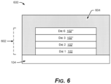
- FIG. 6 is a diagram of an example module with a die stack that includes a molding feature for alleviating a warpage stress in the vertical stack.
- FIG. 7 is a flow diagram of an example process for fabricating the example module of FIG. 6 .
- FIG. 8 is a diagram of an example module with a vertical die stack, including a relief cavity feature for alleviating a warpage stress in the vertical stack.
- FIG. 9 is a flow diagram of an example process for fabricating the example module of FIG. 8 .
- FIG. 10 is a diagram of an example module with a die stack that includes a stress balancing layer feature for alleviating a warpage stress in the vertical stack.
- FIG. 11 is a flow diagram of an example process for fabricating the example module of FIG. 10 .
- FIG. 12 is a diagram of an example module of vertically stacked dies with at least some rounded corners or edges to prevent stress concentration at corners.
- FIG. 13 is a flow diagram of an example process for preventing concentration of damaging forces in fabrication of a vertical stack of dies.
- FIG. 14 is a diagram of an example module with multiple thin dies substituting for a large die to reduce stress warpage in a die stack.
- FIG. 15 is a diagram of an example structure including a lateral support for eliminating warpage problems and increasing yield in fabrication of modules with vertical die stacks.
- FIG. 16 is a diagram of an example structure with no top die spacer, and with lateral support structures and molding, for reducing interior stresses.
- FIG. 17 is a diagram of example structures formed in a process that uses temperature differentials to reduce warpage stresses during fabrication of vertical stacks of dies.
- FIG. 18 is a diagram of example structures and associated processes for making an example module of stacked dies by uniting multiple pre-made stacks of dies, while reducing interior stress warpage.
- FIG. 19 is a diagram of an example structure with features for alleviating warpage stresses in stacks of dies, including rounded die corners supported by an encapsulant fillet or wedge.
- FIG. 20 is a diagram of example structures for constructing larger modules that have numerous stacked dies, without introducing problems caused by stress warpage.
- FIG. 21 is a diagram of example structures including thin layers of dielectric material and features for reducing interior stresses.
- FIG. 22 is another diagram of example structures possible that include features for reducing interior stresses.
- FIG. 23 is a diagram of an example structure with one or more direct bonded die stacks incorporating stress-relief measures, a processor, and optional heat sink.
- This disclosure describes direct bonded stack structures for increased reliability and improved yields in microelectronics.
- Structural features and stack configurations are provided for memory modules, stacked passive elements, interposers, and 3DICs to reduce both severe and minor defects in vertically stacked dies.
- Example processes and structures alleviate stresses, such as warpage stresses, between a thicker top die and direct bonded dies beneath it or a thinner top die directly bonded to a thicker die beneath, for example.
- a surface that has been ground and etched on the top die may relieve stresses, such as warpage stresses, of the stack of dies.
- the example stack may include a compliant layer between the top die and dies beneath it to relieve warpage stresses.
- another stack configuration replaces the top die with a layer of molding material to circumvent warpage stresses.
- an array of cavities on the bonding surface of the top die or elsewhere can alleviate stress forces.
- a stress balancing layer may also be created on the topside or backside of the top die to relieve warpage stresses of the stack, or one or more stress balancing layers can intervene between other dies in a stack of dies.
- right-angle corners of some dies in a stack are rounded to prevent concentration of pressing forces at square corners of dies during stack fabrication, and to prevent transmission of those concentrated forces to relatively fragile dies or substrate layer below or above, cracking and chipping them.
- Example processes fabricate stack structures with structural features and configurations to reduce severe and minor defects that can occur in vertical stacks of direct bonded dies.
- Memory modules include, but are not limited to, 3DS®, HMC hybrid memory cube, HBM, HBM2 and HBM3, which are described below as representative examples, but the described technology can be applied to any microelectronics package with vertically stacked dies, especially dies that are direct bonded together, and the structures and techniques described herein are not limited to memory modules.
- FIG. 2 shows an example memory module 200 with a die stack 202 that includes a feature for alleviating a warpage stress in the vertical stack 202 .
- the top die 106 of the stack 202 has a surface that is treated by grinding 204 and then either wet etching 206 or dry etching 206 to relieve a warpage 112 or an internal stress of the top die 106 , thus decreasing or eliminating its concavity 112 in some cases.
- the etching 206 relieves pent up stress from the grinding operation 204 . This in turn helps to relieve defects resulting from stress forces that can occur between the top die 106 and the dies 102 beneath it.
- substrate 104 may be an organic or inorganic structure, such as a circuit board, package substrate, die, wafer, carrier etc, which may be electrically coupled to the stack 202 , including coupling at least in part through direct and/or hybrid bonding, eutectic bonding, etc.
- FIG. 3 shows an example process 300 for making the structure 200 of FIG. 2 .
- operations of the example process are shown in individual blocks.
- the example process includes direct bonding dies 102 together to make part of the vertical stack 202 .
- the top die 106 is prepared for bonding to the top of the other dies 102 to form vertical stack 202 .
- the backside of the top die 106 is ground.
- the backside of the top die 106 is then wet etched 206 or dry etched for stress relief.
- the top die 106 is then bonded to the dies below 102 , to produce a microelectronics package 200 of vertically stacked dies 102 & 106 with reduced internal stress and increased reliability, thereby alleviating a warpage stress between the top die 106 and the dies 102 in the vertical stack beneath the top die 106 .
- FIG. 4 shows an example memory module 400 with a die stack 402 that includes a feature for alleviating a warpage stress in the vertical stack 402 .
- the vertical stack 402 is fabricated with a compliant layer 404 intervening in between the top die 106 and the dies 102 direct bonded to each other beneath the top die 106 .
- the top die may have different vertical and/or horizontal dimensions than at least one other die in the direct bonded die stack 400 .
- the compliant layer 404 is intended to cushion uneven forces during bonding of the top die 106 to the vertical stack 402 , and to counteract or dissipate ongoing unevenness of stresses and warpage forces between the top die 106 and the dies 102 beneath.
- the thickness of the compliant material or compliant layer 404 may range between 0.5-55.0 microns and preferably between 3.0-30.0 microns.
- the compliant layer 404 may be adhered or bonded between the dies, and can provide a single solution to warpage when the top die 106 is a dummy die for filling the top space of the package 400 .
- the compliant layer 404 may be adhered or bonded between the dies, and can provide a single solution to warpage when the top die 106 is a dummy die for filling the top space of the package 400 .
- the Young's modulus of compliant layer 404 is preferably less than 4 GPa.
- the width of the top die 106 is similar to the width of one of the dies below 102 . In other embodiments, as in stack 400 ′, the width of the top die 106 ′ is different from a width of other dies in the vertical stack 400 ′, and may be wider than the dies 102 below, for example.
- FIG. 5 shows an example process 500 for fabricating the example module 400 of FIG. 4 . Operations of the example process 500 are shown in individual blocks.
- the example process 500 includes direct bonding dies 102 together to make part of a vertical stack 402 .
- a top die 106 is prepared for bonding to the top of the direct bonded dies 102 .
- a compliant layer 404 is applied to interpose between the top die 106 and other dies 102 of the vertical stack 402 , for example.
- the top die 106 is then bonded to the compliant layer 404 .
- the compliant layer may be an adhesive or another compliant material bonded by thin film die attach, printed or stenciled die attach material, or other adhesives, for example.
- the microelectronics package 400 with vertically stacked dies 102 & 106 and compliant layer 404 provides reduced internal stress and increased reliability, alleviating a warpage stress between the top die 106 and the dies 102 of the vertical stack 402 .
- a flowable material that sets may be used for the compliant layer 404 . The dispensed material flows and will accommodate the warpage very well.
- flow is achieved at elevated temperatures and the flowed material also accommodates the height differences across warped dies to alleviate the warpage.
- the width of the top die 106 may be similar or different than the width of the dies below 102 , as in FIG. 4 .
- FIG. 6 shows as example module, a microelectronics package 600 with a die stack 602 that includes a fill feature for alleviating a warpage stress in the vertical stack 602 .
- a volume of molding material 604 , filler, underfill material, etc. substitutes for a top die 106 , which is eliminated in this embodiment.
- the actual dies 102 in the vertical stack 602 remain with a slight but acceptable negative warpage, and the microelectronics package 600 is filled out with the molding compound 604 to complete the microelectronics package 600 .
- the residual negative warpage of the direct bonded dies 102 may also be addressed and alleviated with a stress balancing layer as described with respect to FIGS. 10 - 11 .
- One or more stress balancing layers (not shown in FIG. 6 ) can be applied on or within the stack 602 to counterbalance and cancel out the net warpage of the entire stack 602 . Or, such stress balancing layers can be matched with each individual die 102 to be bonded into the stack 602 .
- Each stress balancing layer is designed to counteract a camber of a warped die or stack, with an opposite camber of its own, before the stress balancing layer and the warped die or stack are mated together, at which point the cambers cancel each other out resulting in a flat stack 602 with a net overall warp of zero.
- the lateral width of the molding material 604 on the either side of the stacked dies 602 is smaller than a width of the dies 102 and preferably less than 10% of the width of the dies 102 .
- the vertical thickness of the molding material abutting the top 102 die is less than the thickness of the die stack 602 and preferably less than 50% of the vertical thickness of the die stack 602 .
- FIG. 7 shows an example process 700 for fabricating the example module 600 of FIG. 6 . Operations of the example process 700 are shown in individual blocks.
- the example process 700 includes direct bonding dies 102 together to make a vertical stack 602 .
- molding material 604 is at least partly filled around the vertical stack 602 to substitute for the volume of the missing top die 106 and to complete the outer physical dimensions of the memory module 600 to specification.
- the thickness of the molding material 604 on top of the vertical stack 602 may be multiples of the thickness of an individual die 102 in the vertical stack 602 .
- the thickness of the molding material 604 may be 3 times the thickness of a die 102 in the vertical stack 602 .
- One or more stress balancing layers may be added anywhere in or around the stack 602 .
- FIG. 8 shows as example module 800 with a die stack 802 that includes a relief cavity feature for alleviating a warpage stress in the vertical stack 802 .
- relief cavities 804 (not to scale) are made in the bonding surface of the top die 106 to relieve coupling forces between the top die 106 and at least the next die 102 ′′′ beneath the top die 106 .
- An array of the relief cavities 804 may be placed where coupling forces are known or determined to be detrimental to the stability of the microelectronics package 800 .
- top die 106 is an active die and part of the electronics of the memory module 800 (and not just a dummy die), then there may be metal interconnects, such as direct bonded interconnects, between the top die 106 and the next die 102 ′′′ beneath. Even though the metal interconnects may be rigid, the array of relief cavities 804 may still reduce and relieve coupling forces between the top die 106 and the vertical stack 802 to decrease the effect of warpage forces in the microelectronics package 800 .
- metal interconnects such as direct bonded interconnects
- the example relief cavities 804 are typically formed in some portions of the dielectric regions between adjacent interconnects. In other applications, the relief cavities 804 may be formed between the interconnect portion and the edges on the die or singulation lanes. Also, the relief cavities 804 may be continuous or discontinuous and the geometrical profile of a relief cavity 804 may be triangular, rectangular or curvilinear. The depth of the relief cavities 804 may range between a few nanometers to a few microns. In an implementation, it is important that in the immediate region of the relief cavities 804 , the bonding surface of the top die 106 is discontinuous from the surface of the die 102 beneath.
- FIG. 9 shows an example process 900 for fabricating the example module 800 of FIG. 8 . Operations of the example process 900 are shown in individual blocks.
- the example process 900 includes direct bonding dies 102 together to make a vertical stack 802 .
- the top die 106 is prepared for direct bonding to the vertical stack 802 .
- relief cavities 804 are created in the top die 106 .
- the top die 106 is bonded or direct bonded to the vertical stack 802 to create a microelectronics package 800 with warpage stresses alleviated between the top die 106 and the dies 102 of the vertical stack 802 to provide a more reliable package with reduced possibility of severe defects.
- FIG. 10 shows as example memory module 1000 with a die stack 1002 that includes a feature for alleviating a warpage stress in the vertical stack 1002 .
- a stress balancing layer 1004 is created on a backside of the top die 106 (topside of the vertical stack 1002 when the vertical stack 1002 includes the top die 106 ).
- the stress balancing layer 1004 may be made of a hard or firm material applied by physical vapor deposition (PVD) methods, for example, or by other application techniques to prevent warpage from occurring in the first place.
- PVD physical vapor deposition
- the stress balancing layer 1004 may also be one or more firm materials to suppress or counteract the warpage of a die or stack, resulting from construction of the package 1000 or resulting from subsequent thermal changes during operation.
- the stress balancing layer 1004 may also be a layer that has a warp or camber of its own, designed to counter and cancel out the warpage or stress of a die or stack to which it will be adhered or bonded.
- the stress balancing layer 1004 in some configurations, can also redistribute stresses, balancing local stresses by horizontal redistribution of local warps and stress points with other local areas that have the opposite warp or stress, for a net zero overall warpage.
- the stress balancing layer 1004 may be coated on the lower side of the top die 106 .
- the stress balancing layer 1004 is disposed between the top die 106 and the bonded die immediately beneath the top die 106 in the stack 1002 ′, such as die 4 102 ′′′ in structure 1000 ′ of FIG. 10 , for example.
- one or more stress balancing layers 1004 may be placed between the thin dies 102 in a die stack 1002 ′′, or anywhere in the stack 1002 ′′.
- Such stress balancing layers 1004 can also be matched with each individual die 102 to be bonded into the stack 1002 ′′.
- Each stress balancing layer 1004 is designed to counteract a camber of a warped die 102 or stack 1002 , with an opposite camber of its own.
- the stress balancing layer 1004 may apply a slight leaf spring action to the die or stack being unwarped. The opposing cambers cancel each other out when each stress balancing layer 1004 is mated to its warped die or stack, resulting in a flat stack 1002 , or flatter stack 1002 , ideally with a net overall warpage of zero.
- a stress balancing structure may comprise the stress balancing layer 1004 and a bonding layer, such as a distinct dielectric layer (not shown) and this bonding layer is disposed between the stress balancing layer 1004 and the bonded die immediately beneath, such as die 4 102 ′′ in FIG. 10 , for example.
- the dielectric bonding layer may be a thin adhesive layer and the thickness of the adhesive layer is substantially thinner than one of the bonded dies 102 .
- an example stress balancing layer 1004 can be made of one or more conductive layers, for example, an example stress balancing layer 1004 may be made of titanium nitride and/or tantalum (TiN/Ta), or Ta and Al as co-evaporated or co-sputtered layers, or these metals may be deposited sequentially over each other. But the example stress balancing layer 1004 is not limited to these compounds and elements. Multiple stress balancing layers 1004 may be applied and may have different coefficients of thermal expansion (CTEs) to provide different balancing force differentials at different temperatures.
- CTEs coefficients of thermal expansion
- a bonding layer such as an oxide, nitride, or similar material may be formed on the stress balancing layer to enable direct or hybrid bonding to another surface.
- the stress balancing layer 1004 may be able to accommodate vertical conductors, such as TSVs and/or metal interconnects transiting through a thickness of the stress balancing layer 1004 .
- the stress balancing layer 1004 can be made of a photopatterned polymer, which assembles or has a tendency to assemble into a curved geometry.
- a differentially photo-crosslinked SU-8 photoresist film may curve upon photolithographic patterning.
- a polymeric thin film with heterogeneous mechanical properties makes a curved or leaf spring stress balancing layer 1004 to be bonded to a warped die.
- FIG. 11 shows an example process 1100 for fabricating the example module 1000 of FIG. 10 including one or more stress balancing layers 1004 . Operations of the example process 1100 are shown in individual blocks.
- the example process 1100 includes direct bonding dies 102 together to make a vertical stack 1002 of the dies 102 .
- a top die 106 is prepared for direct bonding with the vertical stack 1002 .
- the top die 106 is associated with a stress balancing layer 1004 .
- the top die 106 is pre-coated with the stress balancing layer 1004 prior to its attachment to the vertical stack 1002 .
- the new stack may be processed further, for example, undergoing thermal annealing or molding operations.
- the top die 106 and stress balancing layer 1004 are bonded to the dies 102 in the vertical stack 1002 .
- one or more stress balancing layers 1004 are placed anywhere in a stack of dies to balance stresses or cancel warpages of a die, a group of dies, or an entire stack of dies.
- FIG. 12 shows a memory module 1200 of vertically stacked dies 102 direct bonded together.
- Right-angle corners 1204 of some dies 102 in the stack 1202 can be rounded in the x-, y-, and/or z-directions to prevent stress concentration: a concentration of pressing forces 1205 at the conventionally squared corners 1204 of the dies 102 during stack fabrication.
- the pressing forces 1205 can conventionally crack and chip the fragile dies, or the substrate 104 , below the 90 degree corners.
- Rounding, chamfering, or otherwise easing the typically sharp 90 degree corners or the edges between the z-plane and the x/y-planes can prevent or disperse transmission of the concentrated pressing forces 1205 to the relatively fragile and brittle dies, or the substrate 104 , beneath.
- the edges of the bonded dies 102 of stack 1202 are rounded to prevent point stresses at corners 1204 .
- the edges of the top die 106 may also be rounded.
- FIG. 13 shows an example process 1300 for preventing concentration of damaging forces in fabrication of a vertical stack of dies 1202 . Operations of the example process 1300 are shown in individual blocks.
- the example process 1300 includes rounding right-angle corners of selected dies to be made into the vertical stack of dies 1202 .
- the corner-rounding can be achieved, for example, by applying a high pressure dielectric etch during a plasma etching operation.
- the etching operation may comprise etching the substrate 104 and coated dielectric layers.
- the edges of the dielectric of the bonding surface need to be rounded prior to the bonding operation.
- the boding surface may be shielded with a protectant and the selected edges may be rounded by wet etching methods or by mild abrasive powder blasting operations, or by laser jet methods or combinations thereof.
- the dies 102 to be used in the stack 1202 are then lined up according to a vertical plane.
- the dies 102 with at least some rounded corners 1204 are direct bonded together into a stack 1202 , with the rounded corners 1204 preventing pressing forces from concentration at the corners 1204 and also preventing these forces from being transmitted to break, crack, or chip the next die or substrate 104 below.
- FIG. 14 shows another example module 1400 , memory module, or other stacked device, constructed according to one or more techniques for reducing stress warpage in the die stack 1402 making up the module 1400 .
- two or more thinner dies 1404 are bonded on top of the stack 1402 of smaller dies 102 . These thinner dies 1404 on top either conform to the stack below 1402 or can impose a counter-warpage to that of the warpage of the stack 1402 underneath.
- a molding material 1406 laterally surrounds the bonded die stack 1402 .
- FIG. 15 shows another example structure 1500 for eliminating warpage problems and reduced yield in fabrication of modules, such as memory modules and other devices with stacked dies.
- a stack of the dies 102 are provided with a lateral support 1502 , such as side buttresses made of underfill material or another firm solid or particulate composite layer. Since the individual dies 102 can be very thin, such as 55 ⁇ m in thickness or even thinner, they may be prone to warping. Before a thick top die 1504 is bonded to the stack, the lateral supports 1502 are built against the sides of the stack. These one or more lateral die support structures 1502 may be formed by various dispensing methods including printing or molding methods.
- the lateral supports 1502 hold the edges of the dies and also stabilize the stack of dies 102 as a whole.
- a lateral support structure 1502 also reduces incidences of damage to the bonded dies from routine handling operations. This results in a finished module, in which the various dies 102 and 1504 are less prone to chipping or cracking on account of the solid stabilization of the lateral supports 1502 .
- Side molding 1506 may also be added to further stabilize the stack 102 & 1504 and complete the package.
- the lateral support structure 1502 abuts the periphery of the bonded dies 102 and not that of the top die 1504 .
- the side molding 1506 is disposed around the bonded dies 102 and the top die 1504 , but the side molding 1506 is not in direct contact with the lower dies 102 of the stacked bonded dies, such as die “1” 102 and die “2” 102 ′, for example.
- the side molding 1506 directly abuts only some portions of the bonded dies in the bonded dies stack.
- FIG. 16 shows an implementation of a structure 1600 similar to the structure 1500 of FIG. 15 , but the example module 1600 does not use a top extra die 1504 .
- side molding 1602 may be used after the lateral supports 1502 are placed, in order to complete a shorter package 1600 . As described earlier, the side molding 1602 directly abuts some portions of the topmost die or dies, and not the other bonded dies in the bonded dies stack. In one embodiment, the side molding 1602 does not directly contact the stacked bonded dies.
- FIG. 17 shows additional example structures 1700 & 1702 for creating modules with stacked dies 102 while reducing stress warpage when the dies 102 are direct bonded in a stack.
- the example technique also applies when an extra dummy die 1704 is direct bonded on top of the respective stacks with a concavity of warpage that may be different from that of the stack of dies 102 beneath it.
- multiple thin dies 102 are direct bonded together at a first temperature, for example in the approximate range of 140-350° C.
- the top die, the extra dummy die 1704 is then bonded to the stack of dies 102 at a second temperature preferably lower than the first temperature.
- the multiple thin dies 102 may be bonded at a temperature sufficiently high for a metallic bond to form between mating metallic electric contacts between intimately mated dies.
- the mating temperature for the opposing electrical and non-electrical contacts may range between 150-300° C., and preferably between 180-250° C. for a time duration ranging from 45 minutes to 2-4 hours or even longer.
- the bonding temperature depends on the nature of the mating metal layer. In practice, the higher the bonding temperature, the shorter the bonding times and vice versa.
- the stack of dies 102 is allowed to cool to the lower bonding temperature for additional processing if needed before attaching the top extra dummy die 1704 to the upper surface of the last die in the stack of dies 102 .
- the attached dummy die 1704 is then bonded at a temperature preferably lower than the metallic mating temperature of the bonded stacked dies.
- the dummy die 1704 is bonded at temperatures ranging from below room temperature to below 130° C., and preferably below 100° C. Reducing the bonding temperature of the top die 1704 reduces the stress transmitted from the die 1704 to bonded dies beneath, such as in example stacks 602 ( FIG. 6 ), stack 1402 ( FIG. 14 ), and stack 1801 ( FIG. 18 ).
- the warpage state of the stack of dies 102 direct bonded at the higher temperature and then cooler to the lower temperature is memorialized and “fixed” by adding a lateral support 1502 of underfill or other solid material to stabilize the stack.
- the package is stabilized and/or completed with molding material 1706 on sides as needed.
- FIG. 18 shows example structures and associated processes for making an example module 1800 of stacked dies that has reduced interior stress warpage and/or a higher manufacturing yield due to less failure from warpage during fabrication.
- a first stack of dies 1801 is assembled by direct bonding thin dies 102 to each other, or by other bonding means. Underfill or other solid material is used to make lateral supports 1502 for the stack of dies 102 , thereby stabilizing the stack of dies 102 in a non-warped state.
- Another stack 1810 of dies 1802 & 1804 & 1806 & 1808 are made separately, applying one or more of the anti-warping measures as described herein.
- This pre-made stack 1810 of additional dies is then bonded or direct bonded to the initial stack of dies 102 , rather than just continuing the initial single stack 102 by adding the individual additional dies 1802 & 1804 & 1806 & 1808 one-by-one, which would propagate and further exaggerate the negative warpage of the initial stack of dies 102 .
- a layer 1812 topping the initial stack of dies 102 which would be an extra dummy die in conventional modules to fill out the package, is made of active dies 1802 & 1804 in this implementation of the microelectronic device or module 1800 being assembled, these dies 1802 & 1804 are not dummy dies.
- the module 1800 now containing two stacks of dies 102 & 1810 direct bonded together, can be filled out and completed with a molding material 1814 .
- the lateral supports 1502 made of underfill material represent a first encapsulation that touches, supports and stabilizes only the dies 102 of the first stack of dies 102
- the molding material 1814 added later represents a second encapsulation that touches, supports, and stabilizes only the dies of the second stack 1810 .
- all dies in the two stacks 102 and 1810 get stabilized in a non-warped configuration by encapsulants, but in a different manner for each of the stacks as the module 1800 is assembled.
- the first stack of dies 102 receives lateral supports 1502 from a buttressing underfill material, while the next stack of dies 1810 receives non-warp stabilization from side molding 1814 that completes the package.
- FIG. 19 shows another example structure 1900 and method for alleviating warpage stresses in stacks of dies and microchips, especially when the dies are very thin.
- An example module 1900 with a stack 1902 of dies 102 is built on a substrate 104 , such as a semiconductor wafer, carrier, panel, or interposer, etc.
- a top die 1904 is added to the stack of dies 102 to bring the package to a height specification.
- the top die 1904 may be a dummy die, but can also be one or more active dies.
- the top die 1904 is thicker than the individual dies 102 making up the stack 1902 beneath it, and so is subject to warping in its own right.
- the bonding surface of the top die 1904 may be formed by photolithographic and selective material methods.
- the bonding surface of die 1904 may be selectively protected with an organic or inorganic resist protective layer for example.
- the unprotected portion of the bond surface may be etched by a dry or a wet method to remove sufficient materials to prevent the etched regions from contacting the top bonding surface of the die 102 immediately beneath during and after the bonding operation.
- the protective layer is stripped, the bottom bonding surface of the top dies is cleaned, prepared and bonded to the top surface of die 102 .
- the top die 1904 may be imparted with rounded edges on its bonding side proactively.
- the top die 1904 is direct bonded to the stack of dies beneath it at its middle region forming a peripheral gap beyond the bonded region.
- the prepared bonding surface of the top die 1904 is smaller than the bonding surface of die 102 beneath. Reducing the bonded area between top die 1904 and the die beneath, for example die “4” 102 ′′′, reduces the force transmitted to the bonded dies beneath.
- an encapsulant wedge or fillet 1906 may be applied to fill the peripheral gap beyond the bonded region of die 1904 .
- the encapsulant fillet 1906 may comprise or incorporate a particulate material to reduce the thermal expansion of the encapsulant material.
- underfill material or a molding material 1908 may be applied to encapsulate the bonded dies, such as dies 102 and die 1904 , and to fill the fillet 1906 between the top die 1904 and the die 102 ′′′ beneath.
- the encapsulating material 1908 firmly couples the bonded dies stack 102 and the top die 1904 to form an integrated solid structure and also acts as a protective layer thereby preventing stress cracking and delamination between the stack of dies 102 and the top die 1904 .
- the fillet 1906 of compliant material may also be the same material as the molding 1908 around the sides of the stack 102 & 1904 , which completes the package 1900 .
- FIG. 20 shows another example scheme for constructing larger modules 2000 that have numerous stacked dies, without introducing problems caused by stress warpage, which decrease yield during fabrication.
- a compliant layer 2001 is added at intervals, between groups of dies, such as between a first group of dies 102 , a second group 2010 of dies 2002 & 2004 & 2006 & 2008 , and a third group 2012 of active or dummy dies.
- the compliant layer 2001 comprises one or more conductive vias for electrically connecting conductive features on the backside of die “4” 102 ′′′ to the conductive features of die “5” 2002 .
- the layer 2001 may comprise one or more low melting point conductive materials (for example solder) for connecting desirable portions of die “4” 102 ′′′ to similar portions in die “5” 2002 .
- the dies 102 and compliant layers 2001 are stacked up individually, one die 102 or layer 2001 at a time, by direct bonding or direct hybrid bonding, for example.
- the groups of dies 102 & 2010 & 2012 are constructed separately, and groups of dies are added to the overall stack as grouped units.
- the stack may be encapsulated with molding 2014 or the same compliant material as used in the compliant layers 2001 .
- FIG. 21 shows thin dies 2102 direct hybrid-bonded together into stacks 2104 .
- Each stack 2104 is built on a common wafer substrate 2106 , for example, or carrier, panel, etc.
- Thin layers of dielectric and metal 2108 (direct hybrid bonding layers 2108 ) on the dies 2102 and substrate 2106 enable the direct hybrid bonding. That is, the bonding layer 2108 may consist of multiple layers, and/or may consist of a combination of dielectric material(s) and metal(s).
- the dielectric may consist of multilayer dielectrics including but not limited to diffusion barrier layers and dielectric layers for bonding which consist of Si, O, N, and C.
- layer 2108 may also contain metal materials as conductive pads, wherein the direct bonding occurs at the dielectric surfaces followed by direct bonding between metal bonding pads, vias, and interconnects of the dies 2102 in an annealing step of the same overall direct bonding operation.
- One or more extra dummy dies on top of each stack 2104 may be direct bonded to each respective stack 2104 with oxide-oxide direct bonding.
- a singulation operation 2110 dices individual stacks 2104 into individual module units 2112 , such as individual high bandwidth memory modules.
- FIG. 22 shows thin dies 2202 direct hybrid bonded together into stacks 2204 and encapsulated with a molding material 2205 .
- Each stack 2204 is built on a common wafer substrate 2206 , carrier, panel, etc.
- Direct hybrid bonding layer 2208 consists of extremely thin layers of dielectric 2208 on the dies 2202 and substrate 2206 to enable the direct hybrid bonding.
- Thin layers 2208 of dielectric and metal (direct hybrid bonding layer 2108 ) on the dies 2202 and substrate 2206 enable the direct hybrid bonding.
- the bonding layer 2208 may consist of multiple layers, and/or may consist of a combination of dielectric material(s) and metal(s).
- the dielectric may consist of multilayer dielectrics including but not limited to diffusion barrier layers and dielectric layers for bonding which consist of Si, 0 , N, and C. Additionally, layer 2208 may also contain metal materials as conductive pads, wherein the direct bonding occurs at the dielectric surfaces followed by direct bonding between metal bonding pads, vias, and interconnects of the dies 2202 in an annealing step of the same overall direct bonding operation. One or more extra dummy dies on top of each stack 2204 may be direct bonded to each respective stack 2204 with oxide-oxide direct bonding, for example.
- a singulation operation 2210 dices individual stacks 2204 into individual module units 2212 that are pre-encapsulated 2205 .
- FIG. 23 shows an example module 2300 with one or more direct bonded die stacks 2302 on a substrate 2304 or board, and a microprocessor 2306 and/or graphics processor, or microcontroller, mounted on the same substrate 2304 or board.
- Each of the one or more direct bonded die stacks 2302 incorporates one of the described stress or warpage-relief measures or stress-warpage prevention devices of FIGS. 2 - 22 .
- the microprocessor 2306 or other logic unit or processor is communicatively coupled with the one or more direct bonded die stacks 2302 .
- Thin layers 2303 of dielectric and metal (direct hybrid bonding layer 2303 ) on the dies 2305 and substrate 2304 enable the direct hybrid bonding.
- the bonding layer 2303 may consist of multiple layers, and/or may consist of a combination of dielectric material(s) and metal(s).
- the dielectric may consist of multilayer dielectrics including but not limited to diffusion barrier layers and dielectric layers for bonding which consist of Si, O, N, and C. Additionally, layer 2303 may also contain metal materials as conductive pads, wherein the direct bonding occurs at the dielectric surfaces followed by direct bonding between metal bonding pads, vias, and interconnects of the dies 2305 in an annealing step of the same overall direct bonding operation.
- the module 2300 includes at least one heat sink 2308 , and in an implementation, the one or more die stacks 2302 and the microprocessor 2306 are in contact with a common heat sink 2308 .
Abstract
Description
Claims (55)
Priority Applications (1)
| Application Number | Priority Date | Filing Date | Title |
|---|---|---|---|
| US17/681,563 US11955463B2 (en) | 2019-06-26 | 2022-02-25 | Direct bonded stack structures for increased reliability and improved yield in microelectronics |
Applications Claiming Priority (3)
| Application Number | Priority Date | Filing Date | Title |
|---|---|---|---|
| US201962866965P | 2019-06-26 | 2019-06-26 | |
| US16/911,360 US11296053B2 (en) | 2019-06-26 | 2020-06-24 | Direct bonded stack structures for increased reliability and improved yield in microelectronics |
| US17/681,563 US11955463B2 (en) | 2019-06-26 | 2022-02-25 | Direct bonded stack structures for increased reliability and improved yield in microelectronics |
Related Parent Applications (1)
| Application Number | Title | Priority Date | Filing Date |
|---|---|---|---|
| US16/911,360 Continuation US11296053B2 (en) | 2019-06-26 | 2020-06-24 | Direct bonded stack structures for increased reliability and improved yield in microelectronics |
Publications (2)
| Publication Number | Publication Date |
|---|---|
| US20220293567A1 US20220293567A1 (en) | 2022-09-15 |
| US11955463B2 true US11955463B2 (en) | 2024-04-09 |
Family
ID=74044084
Family Applications (2)
| Application Number | Title | Priority Date | Filing Date |
|---|---|---|---|
| US16/911,360 Active US11296053B2 (en) | 2019-06-26 | 2020-06-24 | Direct bonded stack structures for increased reliability and improved yield in microelectronics |
| US17/681,563 Active US11955463B2 (en) | 2019-06-26 | 2022-02-25 | Direct bonded stack structures for increased reliability and improved yield in microelectronics |
Family Applications Before (1)
| Application Number | Title | Priority Date | Filing Date |
|---|---|---|---|
| US16/911,360 Active US11296053B2 (en) | 2019-06-26 | 2020-06-24 | Direct bonded stack structures for increased reliability and improved yield in microelectronics |
Country Status (6)
| Country | Link |
|---|---|
| US (2) | US11296053B2 (en) |
| EP (1) | EP3991202A4 (en) |
| JP (1) | JP2022538567A (en) |
| KR (1) | KR20220026536A (en) |
| CN (1) | CN114008766A (en) |
| WO (1) | WO2020264167A1 (en) |
Families Citing this family (54)
| Publication number | Priority date | Publication date | Assignee | Title |
|---|---|---|---|---|
| US7109092B2 (en) | 2003-05-19 | 2006-09-19 | Ziptronix, Inc. | Method of room temperature covalent bonding |
| US7485968B2 (en) | 2005-08-11 | 2009-02-03 | Ziptronix, Inc. | 3D IC method and device |
| US8735219B2 (en) | 2012-08-30 | 2014-05-27 | Ziptronix, Inc. | Heterogeneous annealing method and device |
| US10886250B2 (en) | 2015-07-10 | 2021-01-05 | Invensas Corporation | Structures and methods for low temperature bonding using nanoparticles |
| US10204893B2 (en) | 2016-05-19 | 2019-02-12 | Invensas Bonding Technologies, Inc. | Stacked dies and methods for forming bonded structures |
| US10580735B2 (en) | 2016-10-07 | 2020-03-03 | Xcelsis Corporation | Stacked IC structure with system level wiring on multiple sides of the IC die |
| US11176450B2 (en) | 2017-08-03 | 2021-11-16 | Xcelsis Corporation | Three dimensional circuit implementing machine trained network |
| US10002844B1 (en) | 2016-12-21 | 2018-06-19 | Invensas Bonding Technologies, Inc. | Bonded structures |
| TWI782939B (en) | 2016-12-29 | 2022-11-11 | 美商英帆薩斯邦德科技有限公司 | Bonded structures with integrated passive component |
| US10629577B2 (en) | 2017-03-16 | 2020-04-21 | Invensas Corporation | Direct-bonded LED arrays and applications |
| US10515913B2 (en) | 2017-03-17 | 2019-12-24 | Invensas Bonding Technologies, Inc. | Multi-metal contact structure |
| US10269756B2 (en) | 2017-04-21 | 2019-04-23 | Invensas Bonding Technologies, Inc. | Die processing |
| US10879212B2 (en) | 2017-05-11 | 2020-12-29 | Invensas Bonding Technologies, Inc. | Processed stacked dies |
| US10446441B2 (en) | 2017-06-05 | 2019-10-15 | Invensas Corporation | Flat metal features for microelectronics applications |
| US10840205B2 (en) | 2017-09-24 | 2020-11-17 | Invensas Bonding Technologies, Inc. | Chemical mechanical polishing for hybrid bonding |
| US11031285B2 (en) | 2017-10-06 | 2021-06-08 | Invensas Bonding Technologies, Inc. | Diffusion barrier collar for interconnects |
| US11380597B2 (en) | 2017-12-22 | 2022-07-05 | Invensas Bonding Technologies, Inc. | Bonded structures |
| US10923408B2 (en) | 2017-12-22 | 2021-02-16 | Invensas Bonding Technologies, Inc. | Cavity packages |
| US10727219B2 (en) | 2018-02-15 | 2020-07-28 | Invensas Bonding Technologies, Inc. | Techniques for processing devices |
| US11169326B2 (en) | 2018-02-26 | 2021-11-09 | Invensas Bonding Technologies, Inc. | Integrated optical waveguides, direct-bonded waveguide interface joints, optical routing and interconnects |
| US11056348B2 (en) | 2018-04-05 | 2021-07-06 | Invensas Bonding Technologies, Inc. | Bonding surfaces for microelectronics |
| US10790262B2 (en) | 2018-04-11 | 2020-09-29 | Invensas Bonding Technologies, Inc. | Low temperature bonded structures |
| US10964664B2 (en) | 2018-04-20 | 2021-03-30 | Invensas Bonding Technologies, Inc. | DBI to Si bonding for simplified handle wafer |
| US11004757B2 (en) | 2018-05-14 | 2021-05-11 | Invensas Bonding Technologies, Inc. | Bonded structures |
| US11276676B2 (en) | 2018-05-15 | 2022-03-15 | Invensas Bonding Technologies, Inc. | Stacked devices and methods of fabrication |
| US11393779B2 (en) | 2018-06-13 | 2022-07-19 | Invensas Bonding Technologies, Inc. | Large metal pads over TSV |
| EP3807927A4 (en) | 2018-06-13 | 2022-02-23 | Invensas Bonding Technologies, Inc. | Tsv as pad |
| US10910344B2 (en) | 2018-06-22 | 2021-02-02 | Xcelsis Corporation | Systems and methods for releveled bump planes for chiplets |
| US11664357B2 (en) | 2018-07-03 | 2023-05-30 | Adeia Semiconductor Bonding Technologies Inc. | Techniques for joining dissimilar materials in microelectronics |
| WO2020010265A1 (en) | 2018-07-06 | 2020-01-09 | Invensas Bonding Technologies, Inc. | Microelectronic assemblies |
| WO2020010136A1 (en) | 2018-07-06 | 2020-01-09 | Invensas Bonding Technologies, Inc. | Molded direct bonded and interconnected stack |
| US11515291B2 (en) | 2018-08-28 | 2022-11-29 | Adeia Semiconductor Inc. | Integrated voltage regulator and passive components |
| US11158573B2 (en) | 2018-10-22 | 2021-10-26 | Invensas Bonding Technologies, Inc. | Interconnect structures |
| CN113330557A (en) | 2019-01-14 | 2021-08-31 | 伊文萨思粘合技术公司 | Bonding structure |
| US11901281B2 (en) | 2019-03-11 | 2024-02-13 | Adeia Semiconductor Bonding Technologies Inc. | Bonded structures with integrated passive component |
| US10854578B2 (en) | 2019-03-29 | 2020-12-01 | Invensas Corporation | Diffused bitline replacement in stacked wafer memory |
| US11610846B2 (en) | 2019-04-12 | 2023-03-21 | Adeia Semiconductor Bonding Technologies Inc. | Protective elements for bonded structures including an obstructive element |
| US11373963B2 (en) | 2019-04-12 | 2022-06-28 | Invensas Bonding Technologies, Inc. | Protective elements for bonded structures |
| US11205625B2 (en) | 2019-04-12 | 2021-12-21 | Invensas Bonding Technologies, Inc. | Wafer-level bonding of obstructive elements |
| US11296053B2 (en) | 2019-06-26 | 2022-04-05 | Invensas Bonding Technologies, Inc. | Direct bonded stack structures for increased reliability and improved yield in microelectronics |
| US11862602B2 (en) | 2019-11-07 | 2024-01-02 | Adeia Semiconductor Technologies Llc | Scalable architecture for reduced cycles across SOC |
| KR20210066387A (en) * | 2019-11-28 | 2021-06-07 | 삼성전자주식회사 | Semiconductor package |
| US11762200B2 (en) | 2019-12-17 | 2023-09-19 | Adeia Semiconductor Bonding Technologies Inc. | Bonded optical devices |
| US11876076B2 (en) | 2019-12-20 | 2024-01-16 | Adeia Semiconductor Technologies Llc | Apparatus for non-volatile random access memory stacks |
| CN115088068A (en) | 2019-12-23 | 2022-09-20 | 伊文萨思粘合技术公司 | Electrical redundancy for bonded structures |
| US11721653B2 (en) | 2019-12-23 | 2023-08-08 | Adeia Semiconductor Bonding Technologies Inc. | Circuitry for electrical redundancy in bonded structures |
| US11742314B2 (en) | 2020-03-31 | 2023-08-29 | Adeia Semiconductor Bonding Technologies Inc. | Reliable hybrid bonded apparatus |
| US11735523B2 (en) | 2020-05-19 | 2023-08-22 | Adeia Semiconductor Bonding Technologies Inc. | Laterally unconfined structure |
| US11631647B2 (en) | 2020-06-30 | 2023-04-18 | Adeia Semiconductor Bonding Technologies Inc. | Integrated device packages with integrated device die and dummy element |
| US11764177B2 (en) | 2020-09-04 | 2023-09-19 | Adeia Semiconductor Bonding Technologies Inc. | Bonded structure with interconnect structure |
| US11728273B2 (en) | 2020-09-04 | 2023-08-15 | Adeia Semiconductor Bonding Technologies Inc. | Bonded structure with interconnect structure |
| US11264357B1 (en) | 2020-10-20 | 2022-03-01 | Invensas Corporation | Mixed exposure for large die |
| KR20220122155A (en) * | 2021-02-26 | 2022-09-02 | 삼성전자주식회사 | Semiconductor package including dummy chip |
| US20230207525A1 (en) * | 2021-12-24 | 2023-06-29 | Intel Corporation | Ic die stacking with mixed hybrid and solder bonding |
Citations (589)
| Publication number | Priority date | Publication date | Assignee | Title |
|---|---|---|---|---|
| US4998665A (en) | 1988-09-07 | 1991-03-12 | Nec Corporation | Bonding structure of substrates and method for bonding substrates |
| US5019673A (en) | 1990-08-22 | 1991-05-28 | Motorola, Inc. | Flip-chip package for integrated circuits |
| US5051802A (en) | 1988-01-22 | 1991-09-24 | Thomson-Csf | Compact image sensor |
| US5087585A (en) | 1989-07-11 | 1992-02-11 | Nec Corporation | Method of stacking semiconductor substrates for fabrication of three-dimensional integrated circuit |
| JPH04337694A (en) | 1991-05-15 | 1992-11-25 | Nec Yamagata Ltd | Resin film protecting electronic component |
| US5322593A (en) | 1991-11-21 | 1994-06-21 | Nec Corporation | Method for manufacturing polyimide multilayer wiring substrate |
| US5729896A (en) | 1996-10-31 | 1998-03-24 | International Business Machines Corporation | Method for attaching a flip chip on flexible circuit carrier using chip with metallic cap on solder |
| US5753536A (en) | 1994-08-29 | 1998-05-19 | Matsushita Electric Industrial Co., Ltd. | Semiconductor device and associated fabrication method |
| US5771555A (en) | 1993-11-01 | 1998-06-30 | Matsushita Electric Industrial Co., Ltd. | Method for producing an electronic component using direct bonding |
| US5854507A (en) | 1998-07-21 | 1998-12-29 | Hewlett-Packard Company | Multiple chip assembly |
| US5956605A (en) | 1996-09-20 | 1999-09-21 | Micron Technology, Inc. | Use of nitrides for flip-chip encapsulation |
| US5985739A (en) | 1994-09-19 | 1999-11-16 | Fraunhofer-Gesellschaft Zur Forderung Der Angewandten Forschung E.V. | Semiconductor structures having advantageous high-frequency characteristics and processes for producing such semiconductor structures |
| US5998808A (en) | 1997-06-27 | 1999-12-07 | Sony Corporation | Three-dimensional integrated circuit device and its manufacturing method |
| US6008126A (en) | 1992-04-08 | 1999-12-28 | Elm Technology Corporation | Membrane dielectric isolation IC fabrication |
| JP2000100679A (en) | 1998-09-22 | 2000-04-07 | Canon Inc | Substrate-to-substrate microregion solid-phase junction method with thinner piece and element structure |
| US6049124A (en) * | 1997-12-10 | 2000-04-11 | Intel Corporation | Semiconductor package |
| EP1011133A1 (en) | 1998-12-14 | 2000-06-21 | Ela Medical | Encapsulated microelectronic SMD component, especially for an active implantable medical device and method for its manufacture |
| US6080640A (en) | 1997-07-11 | 2000-06-27 | Advanced Micro Devices, Inc. | Metal attachment method and structure for attaching substrates at low temperatures |
| US6121688A (en) | 1996-01-19 | 2000-09-19 | Shinko Electric Industries Co., Ltd. | Anisotropic conductive sheet and printed circuit board |
| JP2001102479A (en) | 1999-09-27 | 2001-04-13 | Toshiba Corp | Semiconductor integrated circuit device and manufacturing method thereof |
| US6265775B1 (en) | 1997-01-24 | 2001-07-24 | Micron Technology, Inc. | Flip chip technique for chip assembly |
| JP2001284520A (en) | 2000-04-04 | 2001-10-12 | Matsushita Electric Ind Co Ltd | Circuit board for semiconductor chip mounting, manufacturing method for the circuit board, circuit board for relay connecting, semiconductor device and connecting structure between the semiconductor devices |
| KR20010104643A (en) | 2000-04-28 | 2001-11-26 | 이데이 노부유끼 | Chip-like electronic components, a method of manufacturing the same, a pseudo wafer therefor and a method of manufacturing thereof |
| US20020000328A1 (en) | 2000-06-22 | 2002-01-03 | Kabushiki Kaisha Toshiba | Printed wiring board and manufacturing method thereof |
| US20020003307A1 (en) | 2000-07-05 | 2002-01-10 | Tadatomo Suga | Semiconductor device and method for fabricating the device |
| US6374770B1 (en) | 1995-10-26 | 2002-04-23 | Applied Materials, Inc. | Apparatus for improving film stability of halogen-doped silicon oxide films |
| US20020074668A1 (en) | 2000-12-14 | 2002-06-20 | International Business Machines Corporation | Multi-chip integrated circuit module |
| US6410983B1 (en) | 1999-05-26 | 2002-06-25 | Fujitsu Limited | Semiconductor device having a plurality of multi-chip modules interconnected by a wiring board having an interface LSI chip |
| US6423640B1 (en) | 2000-08-09 | 2002-07-23 | Taiwan Semiconductor Manufacturing Co., Ltd. | Headless CMP process for oxide planarization |
| US6465892B1 (en) | 1999-04-13 | 2002-10-15 | Oki Electric Industry Co., Ltd. | Interconnect structure for stacked semiconductor device |
| JP2002353416A (en) | 2001-05-25 | 2002-12-06 | Sony Corp | Semiconductor storage device and manufacturing method therefor |
| JP2002359345A (en) | 2001-03-30 | 2002-12-13 | Toshiba Corp | Semiconductor device and its manufacturing method |
| US6500694B1 (en) | 2000-03-22 | 2002-12-31 | Ziptronix, Inc. | Three dimensional device integration method and integrated device |
| US6582991B1 (en) | 2000-12-14 | 2003-06-24 | Matsushita Electric Industrial Co., Ltd. | Semiconductor device and method for fabricating the same |
| US20030148591A1 (en) | 2002-02-07 | 2003-08-07 | Jan-Dar Guo | Method of forming semiconductor device |
| US6686588B1 (en) | 2001-01-16 | 2004-02-03 | Amkor Technology, Inc. | Optical module with lens integral holder |
| KR20040020827A (en) | 2002-09-02 | 2004-03-09 | 신꼬오덴기 고교 가부시키가이샤 | Semiconductor chip and fabrication method thereof |
| US6713857B1 (en) | 2002-12-05 | 2004-03-30 | Ultra Tera Corporation | Low profile stacked multi-chip semiconductor package with chip carrier having opening and fabrication method of the semiconductor package |
| US20040084414A1 (en) | 2002-08-19 | 2004-05-06 | Kenji Sakai | Polishing method and polishing composition used for polishing |
| JP2004193493A (en) | 2002-12-13 | 2004-07-08 | Nec Machinery Corp | Method and device for picking up die |
| US20040140546A1 (en) | 2003-01-22 | 2004-07-22 | I-Tseng Lee | [stack chip package structure] |
| US6768208B2 (en) | 2000-05-19 | 2004-07-27 | Megic Corporation | Multiple chips bonded to packaging structure with low noise and multiple selectable functions |
| US20040157407A1 (en) | 2003-02-07 | 2004-08-12 | Ziptronix | Room temperature metal direct bonding |
| US6782610B1 (en) | 1999-05-21 | 2004-08-31 | North Corporation | Method for fabricating a wiring substrate by electroplating a wiring film on a metal base |
| US20040188501A1 (en) | 2003-03-31 | 2004-09-30 | Peter Tolchinsky | Complete device layer transfer without edge exclusion via direct wafer bonding and constrained bond-strengthening process |
| US20040238927A1 (en) | 2003-03-17 | 2004-12-02 | Ikuya Miyazawa | Method of manufacturing semiconductor device, semiconductor device, circuit substrate and electronic apparatus |
| US20050040530A1 (en) | 2003-07-31 | 2005-02-24 | Fong Shi | Near hermetic power chip on board device and manufacturing method therefor |
| US6867073B1 (en) | 2003-10-21 | 2005-03-15 | Ziptronix, Inc. | Single mask via method and device |
| US6887769B2 (en) | 2002-02-06 | 2005-05-03 | Intel Corporation | Dielectric recess for wafer-to-wafer and die-to-die metal bonding and method of fabricating the same |
| US20050101130A1 (en) | 2003-11-07 | 2005-05-12 | Applied Materials, Inc. | Method and tool of chemical doping CoW alloys with Re for increasing barrier properties of electroless capping layers for IC Cu interconnects |
| US20050104196A1 (en) | 2003-11-18 | 2005-05-19 | Denso Corporation | Semiconductor package |
| US20050133930A1 (en) | 2003-12-17 | 2005-06-23 | Sergey Savastisuk | Packaging substrates for integrated circuits and soldering methods |
| US20050153522A1 (en) | 2004-01-09 | 2005-07-14 | Hyeon Hwang | Wafer level chip stack method |
| US20050161808A1 (en) | 2004-01-22 | 2005-07-28 | Anderson Douglas G. | Wafer, intermediate wafer assembly and associated method for fabricating a silicon on insulator wafer having an improved edge profile |
| US20050218518A1 (en) | 2002-01-07 | 2005-10-06 | Tongbi Jiang | Semiconductor device assemblies and packages including multiple semiconductor device components |
| US20060057945A1 (en) | 2004-09-16 | 2006-03-16 | Chia-Lin Hsu | Chemical mechanical polishing process |
| US20060063312A1 (en) | 2004-06-30 | 2006-03-23 | Nec Electronics Corporation | Semiconductor device and method for manufacturing the same |
| US20060087042A1 (en) | 2004-10-26 | 2006-04-27 | Sanyo Electric Co., Ltd. | Semiconductor device and manufacturing method of the same |
| US7045453B2 (en) | 2002-10-24 | 2006-05-16 | International Business Machines Corporation | Very low effective dielectric constant interconnect structures and methods for fabricating the same |
| US7105980B2 (en) | 2002-07-03 | 2006-09-12 | Sawtek, Inc. | Saw filter device and method employing normal temperature bonding for producing desirable filter production and performance characteristics |
| WO2006100444A1 (en) | 2005-03-22 | 2006-09-28 | Cambridge Display Technology Limited | Apparatus and method for increased device lifetime in an organic electro-luminescent device. |
| US20060223216A1 (en) | 2005-03-29 | 2006-10-05 | Chin-Huang Chang | Sensor module structure and method for fabricating the same |
| US20060220256A1 (en) | 2005-03-31 | 2006-10-05 | Shim Il K | Encapsulant cavity integrated circuit package system |
| US20060234473A1 (en) | 2005-04-18 | 2006-10-19 | Lawrence Wong | Thin passivation layer on 3D devices |
| US7126212B2 (en) | 1999-10-01 | 2006-10-24 | Ziptronix, Inc. | Three dimensional device integration method and integrated device |
| US20060278331A1 (en) | 2005-06-14 | 2006-12-14 | Roger Dugas | Membrane-based chip tooling |
| US20070007639A1 (en) | 2005-06-24 | 2007-01-11 | Motohiko Fukazawa | Semiconductor device, manufacturing method for semiconductor device, and electronic equipment |
| US7193423B1 (en) | 2005-12-12 | 2007-03-20 | International Business Machines Corporation | Wafer-to-wafer alignments |
| US20070080442A1 (en) | 2004-03-18 | 2007-04-12 | Georg Meyer-Berg | Semiconductor module having a coupling substrate, and methods for its production |
| US20070096294A1 (en) | 2003-06-06 | 2007-05-03 | Sanyo Electric Co., Ltd. | Semiconductor device and manufacturing method of the same |
| US20070111386A1 (en) | 2002-02-20 | 2007-05-17 | Kim Sarah E | Process of vertically stacking multiple wafers supporting different active integrated circuit (IC) devices |
| US20070123061A1 (en) | 2005-11-25 | 2007-05-31 | Advanced Laser Separation International B.V. | Method of treating a substrate, method of processing a substrate using a laser beam, and arrangement |
| US20070122635A1 (en) | 2003-11-24 | 2007-05-31 | Su-Tsai Lu | Bonding Structure With Buffer Layer And Method Of Forming The Same |
| US20070148912A1 (en) | 2005-12-22 | 2007-06-28 | Etsurou Morita | Method for Manufacturing Direct Bonded SOI Wafer and Direct Bonded SOI Wafer Manufactured by the Method |
| US20070158024A1 (en) | 2006-01-11 | 2007-07-12 | Symbol Technologies, Inc. | Methods and systems for removing multiple die(s) from a surface |
| US20070158827A1 (en) | 2005-12-15 | 2007-07-12 | Josef Schuster | Electronic device comprising at least one printed circuit board and comprising a plurality of semiconductor components of identical type, and method |
| US7262492B2 (en) | 2004-09-28 | 2007-08-28 | Intel Corporation | Semiconducting device that includes wirebonds |
| US20070222048A1 (en) | 2006-03-24 | 2007-09-27 | Advanced Semiconductor Engineering, Inc. | Package structure |
| JP2007294724A (en) | 2006-04-26 | 2007-11-08 | Toppan Printing Co Ltd | Multilayer circuit wiring substrate and semiconductor device |
| US20070295456A1 (en) | 2006-03-28 | 2007-12-27 | Innovative Micro Technology | Wafer bonding material with embedded conductive particles |
| US7319197B2 (en) | 2002-05-23 | 2008-01-15 | International Business Machines Corporation | Structure of stacked vias in multiple layer electrode device carriers |
| US20080036082A1 (en) | 2006-08-08 | 2008-02-14 | Samsung Electronics Co., Ltd. | Multi-chip package having a stacked plurality of different sized semiconductor chips, and method of manufacturing the same |
| US20080079105A1 (en) | 2006-09-28 | 2008-04-03 | Siliconware Precision Industries Co., Ltd. | Sensor-type package and fabrication method thereof |
| US7354798B2 (en) | 2002-12-20 | 2008-04-08 | International Business Machines Corporation | Three-dimensional device fabrication method |
| JP2008130603A (en) | 2006-11-16 | 2008-06-05 | Toshiba Corp | Wafer level package for image sensor and manufacturing method therefor |
| US7385283B2 (en) | 2006-06-27 | 2008-06-10 | Taiwan Semiconductor Manufacturing Co., Ltd. | Three dimensional integrated circuit and method of making the same |
| US20080165521A1 (en) | 2007-01-09 | 2008-07-10 | Kerry Bernstein | Three-dimensional architecture for self-checking and self-repairing integrated circuits |
| US20080227238A1 (en) | 2007-03-16 | 2008-09-18 | Ko Wonjun | Integrated circuit package system employing multi-package module techniques |
| WO2008112101A2 (en) | 2007-03-14 | 2008-09-18 | Aptina Imaging Corporation | Packaging methods for imager devices |
| US20080231311A1 (en) | 2005-12-21 | 2008-09-25 | International Business Machines Corp. | Physically highly secure multi-chip assembly |
| US20080268614A1 (en) | 2007-04-25 | 2008-10-30 | Ku-Feng Yang | Wafer Bonding |
| US20080265421A1 (en) | 2007-04-30 | 2008-10-30 | Infineon Technologies Ag | Structure for Electrostatic Discharge in Embedded Wafer Level Packages |
| US20080272477A1 (en) | 2007-05-04 | 2008-11-06 | Stats Chippac, Ltd. | Package-on-Package Using Through-Hole Via Die on Saw Streets |
| US20080308928A1 (en) | 2007-06-13 | 2008-12-18 | Industrial Technology Research Institute | Image sensor module with a three-dimensional die-stacking structure |
| US20080315372A1 (en) | 2007-06-20 | 2008-12-25 | Stats Chippac, Ltd. | Wafer Level Integration Package |
| WO2009005898A1 (en) | 2007-06-28 | 2009-01-08 | Spansion Llc | Die attachment, die stacking, and wire embedding using film |
| US20090029274A1 (en) | 2007-07-25 | 2009-01-29 | 3M Innovative Properties Company | Method for removing contamination with fluorinated compositions |
| US20090068831A1 (en) | 2005-08-11 | 2009-03-12 | Ziptronix | 3d ic method and device |
| US20090095399A1 (en) | 2004-12-28 | 2009-04-16 | Commissariat A L'energie Atomique | Method for trimming a structure obtained by the assembly of two plates |
| US20090149023A1 (en) | 2004-08-20 | 2009-06-11 | Zycube Co., Ltd. | Method of fabricating semiconductor device having three-dimensional stacked structure |
| JP2009135348A (en) | 2007-12-03 | 2009-06-18 | Panasonic Corp | Semiconductor chip, semiconductor device and method of manufacturing them |
| US7554203B2 (en) | 2006-06-30 | 2009-06-30 | Intel Corporation | Electronic assembly with stacked IC's using two or more different connection technologies and methods of manufacture |
| US7566634B2 (en) | 2004-09-24 | 2009-07-28 | Interuniversitair Microelektronica Centrum (Imec) | Method for chip singulation |
| US20090206461A1 (en) | 2008-02-15 | 2009-08-20 | Qimonda Ag | Integrated circuit and method |
| US20090227089A1 (en) | 2008-03-07 | 2009-09-10 | Plaut David J | Dicing tape and die attach adhesive with patterned backing |
| US7589409B2 (en) | 2003-11-04 | 2009-09-15 | Tessera, Inc. | Stacked packages and microelectronic assemblies incorporating the same |
| US20090252939A1 (en) | 2008-04-07 | 2009-10-08 | Samsung Electronics Co., Ltd. | Wafer structures and wafer bonding methods |
| US20090273094A1 (en) | 2008-05-02 | 2009-11-05 | Jong-Woo Ha | Integrated circuit package on package system |
| US20090283898A1 (en) | 2008-05-15 | 2009-11-19 | Janzen Jeffery W | Disabling electrical connections using pass-through 3d interconnects and associated systems and methods |
| US20090321939A1 (en) | 2008-06-30 | 2009-12-31 | Qualcomm Incorporated | Through Silicon via Bridge Interconnect |
| JP2010034294A (en) | 2008-07-29 | 2010-02-12 | Nec Electronics Corp | Semiconductor device and method of designing the same |
| WO2010024678A1 (en) | 2008-09-01 | 2010-03-04 | Nederlandse Organisatie Voor Toegepast-Natuurwetenschappelijk Onderzoek Tno | Chip die clamping device and transfer method |
| US20100081236A1 (en) | 2008-10-01 | 2010-04-01 | Samsung Electronics Co., Ltd | Method of manufacturing semiconductor device with embedded interposer |
| JP2010073964A (en) | 2008-09-19 | 2010-04-02 | Fujitsu Microelectronics Ltd | Method of manufacturing semiconductor device |
| US20100123268A1 (en) | 2008-11-19 | 2010-05-20 | Etienne Menard | Printing Semiconductor Elements by Shear-Assisted Elastomeric Stamp Transfer |
| US20100129999A1 (en) | 2005-05-04 | 2010-05-27 | Sun Microsystems, Inc. | Structures and methods for an application of a flexible bridge |
| US20100167534A1 (en) | 2007-11-21 | 2010-07-01 | Ronald Takao Iwata | Method for fabricating a semiconductor chip device having through-silicon-via (tsv) |
| US7750488B2 (en) | 2006-07-10 | 2010-07-06 | Tezzaron Semiconductor, Inc. | Method for bonding wafers to produce stacked integrated circuits |
| US7759751B2 (en) | 2006-04-11 | 2010-07-20 | Sharp Kabushiki Kaisha | Module for optical apparatus and method of producing module for optical apparatus |
| US20100213819A1 (en) | 2009-02-25 | 2010-08-26 | Cok Ronald S | Flexible oled display with chiplets |
| US7786572B2 (en) | 2005-09-13 | 2010-08-31 | Taiwan Semiconductor Manufacturing Company, Ltd. | System in package (SIP) structure |
| US7790578B2 (en) | 2006-11-30 | 2010-09-07 | Fujitsu Limited | Dicing method using volatile protective agent |
| US7803693B2 (en) | 2007-02-15 | 2010-09-28 | John Trezza | Bowed wafer hybridization compensation |
| US20100259166A1 (en) | 2009-04-09 | 2010-10-14 | Cok Ronald S | Flexible oled display with chiplets |
| US20100258952A1 (en) | 2009-04-08 | 2010-10-14 | Interconnect Portfolio Llc | Interconnection of IC Chips by Flex Circuit Superstructure |
| US7816235B2 (en) * | 2004-10-21 | 2010-10-19 | Infineon Technologies Ag | Semiconductor package and method for producing the same |
| KR20100123755A (en) | 2008-03-05 | 2010-11-24 | 더 보드 오브 트러스티즈 오브 더 유니버시티 오브 일리노이 | Stretchable and foldable electronic devies |
| US7843052B1 (en) | 2008-11-13 | 2010-11-30 | Amkor Technology, Inc. | Semiconductor devices and fabrication methods thereof |
| US20100315110A1 (en) | 2009-06-10 | 2010-12-16 | Medtronic, Inc. | Hermeticity testing |
| US20100327424A1 (en) | 2009-06-24 | 2010-12-30 | Henning Braunisch | Multi-chip package and method of providing die-to-die interconnects in same |
| US20110042814A1 (en) | 2009-08-24 | 2011-02-24 | Sony Corporation | Semiconductor device and method for production of semiconductor device |
| US20110049696A1 (en) | 2006-10-10 | 2011-03-03 | Tessera, Inc. | Off-chip vias in stacked chips |
| US20110074033A1 (en) | 2008-02-13 | 2011-03-31 | Erdem Kaltalioglu | Crack Stop Trenches |
| US7932616B2 (en) | 2007-04-04 | 2011-04-26 | Spansion Llc | Semiconductor device sealed in a resin section and method for manufacturing the same |
| EP2339614A1 (en) | 2009-12-22 | 2011-06-29 | Imec | Method for stacking semiconductor chips |
| US7977789B2 (en) | 2005-12-02 | 2011-07-12 | Nepes Corporation | Bump with multiple vias for semiconductor package and fabrication method thereof, and semiconductor package utilizing the same |
| US20110186977A1 (en) | 2010-01-29 | 2011-08-04 | Stats Chippac, Ltd. | Semiconductor Device and Method of Forming Thin Profile WLCSP with Vertical Interconnect over Package Footprint |
| JP2011171614A (en) | 2010-02-22 | 2011-09-01 | Casio Computer Co Ltd | Semiconductor device, and method of manufacturing the same |
| US8026181B2 (en) | 2005-04-14 | 2011-09-27 | Panasonic Corporation | Manufacturing method for semiconductor chips |
| US20110248397A1 (en) | 2008-11-24 | 2011-10-13 | Stmicroelectronics S.R.L. | Semiconductor device having stacked components |
| US8049303B2 (en) | 2007-04-23 | 2011-11-01 | Hitachi, Ltd. | Semiconductor device with power noise suppression |
| US20110278732A1 (en) | 2010-05-13 | 2011-11-17 | Taiwan Semiconductor Manufacturing Company, Ltd. | Interconnect Structures for Substrate |
| US20110278717A1 (en) | 2010-05-13 | 2011-11-17 | Stats Chippac, Ltd. | Semiconductor Device and Method of Embedding Bumps Formed on Semiconductor Die Into Penetrable Adhesive Layer to Reduce Die Shifting During Encapsulation |
| US8064224B2 (en) | 2008-03-31 | 2011-11-22 | Intel Corporation | Microelectronic package containing silicon patches for high density interconnects, and method of manufacturing same |
| US20110290552A1 (en) | 2004-09-27 | 2011-12-01 | Qualcomm Mems Technologies, Inc. | Method and system for packaging mems devices with incorporated getter |
| US20120003792A1 (en) | 2007-09-10 | 2012-01-05 | Bok Eng Cheah | Stacked die package |
| US20120025396A1 (en) | 2010-07-28 | 2012-02-02 | Chih-Chin Liao | Semiconductor device with die stack arrangement including staggered die and efficient wire bonding |
| US20120049344A1 (en) | 2010-08-25 | 2012-03-01 | Stats Chippac, Ltd. | Semiconductor Device and Method of Forming FO-WLCSP with Discrete Semiconductor Components Mounted Under and Over Semiconductor Die |
| US20120056314A1 (en) | 2010-09-02 | 2012-03-08 | Stats Chippac, Ltd. | Semiconductor Device and Method of Forming Base Leads from Base Substrate as Standoff for Stacking Semiconductor Die |
| US20120077314A1 (en) | 2010-09-28 | 2012-03-29 | Samsung Electronics Co., Ltd. | Method of fabricating semiconductor stack package |
| US20120074585A1 (en) | 2010-09-24 | 2012-03-29 | Stats Chippac, Ltd. | Semiconductor Device and Method of Forming TSV Interposer With Semiconductor Die and Build-Up Interconnect Structure on Opposing Surfaces of the Interposer |
| US8168458B2 (en) | 2008-12-08 | 2012-05-01 | Stats Chippac, Ltd. | Semiconductor device and method of forming bond wires and stud bumps in recessed region of peripheral area around the device for electrical interconnection to other devices |
| US8178964B2 (en) | 2007-03-30 | 2012-05-15 | Advanced Chip Engineering Technology, Inc. | Semiconductor device package with die receiving through-hole and dual build-up layers over both side-surfaces for WLP and method of the same |
| US8178963B2 (en) | 2007-01-03 | 2012-05-15 | Advanced Chip Engineering Technology Inc. | Wafer level package with die receiving through-hole and method of the same |
| US20120119360A1 (en) | 2010-11-16 | 2012-05-17 | Kim Youngchul | Integrated circuit packaging system with connection structure and method of manufacture thereof |
| US8193632B2 (en) | 2008-08-06 | 2012-06-05 | Industrial Technology Research Institute | Three-dimensional conducting structure and method of fabricating the same |
| US20120190187A1 (en) | 2009-10-08 | 2012-07-26 | International Business Machines Corporation | Pad bonding employing a self-aligned plated liner for adhesion enhancement |
| US20120187516A1 (en) | 2011-01-25 | 2012-07-26 | Sony Corporation | Solid-state imaging elements, method for manufacturing solid-state imaging element, and electronic device |
| US20120194719A1 (en) | 2011-02-01 | 2012-08-02 | Scott Churchwell | Image sensor units with stacked image sensors and image processors |
| US20120199960A1 (en) | 2011-02-07 | 2012-08-09 | Texas Instruments Incorporated | Wire bonding for interconnection between interposer and flip chip die |
| US8241961B2 (en) | 2008-12-09 | 2012-08-14 | Young Hae KIM | Method for manufacturing hetero-bonded wafer |
| US20120212384A1 (en) | 2011-02-17 | 2012-08-23 | International Business Machines Corporation | Integrated antenna for rfic package applications |
| US20120217644A1 (en) | 2011-02-24 | 2012-08-30 | Stats Chippac, Ltd. | Semiconductor Device and Method of Forming Conductive THV and RDL on Opposite Sides of Semiconductor Die for RDL-to-RDL Bonding |
| US8263434B2 (en) | 2009-07-31 | 2012-09-11 | Stats Chippac, Ltd. | Semiconductor device and method of mounting die with TSV in cavity of substrate for electrical interconnect of Fi-PoP |
| US20120238070A1 (en) | 2011-03-16 | 2012-09-20 | Memc Electronic Materials, Inc. | Methods for producing silicon on insulator structures having high resistivity regions in the handle wafer |
| US8314007B2 (en) | 2009-12-23 | 2012-11-20 | Soitec | Process for fabricating a heterostructure with minimized stress |
| US20130001798A1 (en) | 2011-07-01 | 2013-01-03 | Samsung Electronics Co., Ltd. | Semiconductor package |
| US8349635B1 (en) | 2008-05-20 | 2013-01-08 | Silicon Laboratories Inc. | Encapsulated MEMS device and method to form the same |
| US20130009325A1 (en) | 2010-03-18 | 2013-01-10 | Nec Corporation | Semiconductor element-embedded substrate, and method of manufacturing the substrate |
| JP2013033786A (en) | 2011-08-01 | 2013-02-14 | Sony Corp | Semiconductor device and semiconductor device manufacturing method |
| US20130037962A1 (en) | 2011-08-09 | 2013-02-14 | Yan Xun Xue | Wafer level packaging structure with large contact area and preparation method thereof |
| US8377798B2 (en) | 2010-11-10 | 2013-02-19 | Taiwan Semiconductor Manufacturing Co., Ltd | Method and structure for wafer to wafer bonding in semiconductor packaging |
| US20130069239A1 (en) | 2011-09-16 | 2013-03-21 | Stats Chippac, Ltd. | Semiconductor Device and Method of Forming Stacked Semiconductor Die and Conductive Interconnect Structure Through an Encapsulant |
| US20130075923A1 (en) | 2011-09-23 | 2013-03-28 | YeongIm Park | Integrated circuit packaging system with encapsulation and method of manufacture thereof |
| US20130082399A1 (en) | 2011-10-04 | 2013-04-04 | Won-keun Kim | Semiconductor package and method of manufacturing the same |
| US8441131B2 (en) | 2011-09-12 | 2013-05-14 | Globalfoundries Inc. | Strain-compensating fill patterns for controlling semiconductor chip package interactions |
| US20130122655A1 (en) | 2010-07-30 | 2013-05-16 | Taiwan Semiconductor Manufacturing Company, Ltd. | Embedded Wafer-Level Bonding Approaches |
| US8456856B2 (en) | 2009-03-30 | 2013-06-04 | Megica Corporation | Integrated circuit chip using top post-passivation technology and bottom structure technology |
| US8476146B2 (en) | 2010-12-03 | 2013-07-02 | Taiwan Semiconductor Manufacturing Company, Ltd. | Reducing wafer distortion through a low CTE layer |
| US8476165B2 (en) | 2009-04-01 | 2013-07-02 | Tokyo Electron Limited | Method for thinning a bonding wafer |
| US20130169355A1 (en) | 2012-01-04 | 2013-07-04 | Kuan-Neng Chen | Integrated Circuit Device |
| US20130187292A1 (en) | 2012-01-20 | 2013-07-25 | Taiwan Semiconductor Manufacturing Company, Ltd. | Multi-Dimensional Integrated Circuit Structures and Methods of Forming the Same |
| US8501537B2 (en) | 2011-03-31 | 2013-08-06 | Soitec | Methods for bonding semiconductor structures involving annealing processes, and bonded semiconductor structures formed using such methods |
| US8513088B2 (en) | 2011-02-04 | 2013-08-20 | Kabushiki Kaisha Toshiba | Semiconductor device and method for manufacturing the same |
| US8519514B2 (en) | 2009-10-09 | 2013-08-27 | Elpida Memory, Inc. | Semiconductor device and manufacturing method thereof |
| US20130234320A1 (en) | 2012-03-09 | 2013-09-12 | Industrial Technology Research Institute | Chip stack structure and method for fabricating the same |
| US20130265733A1 (en) | 2012-04-04 | 2013-10-10 | Texas Instruments Incorporated | Interchip communication using an embedded dielectric waveguide |
| US20130264684A1 (en) | 2012-04-09 | 2013-10-10 | Taiwan Semiconductor Manufacturing Company, Ltd. | Methods and Apparatus of Wafer Level Package for Heterogeneous Integration Technology |
| US20130277855A1 (en) | 2012-04-24 | 2013-10-24 | Terry (Teckgyu) Kang | High density 3d package |
| US20130299997A1 (en) | 2010-07-15 | 2013-11-14 | Soitec | Methods of forming bonded semiconductor structures |
| US20130334697A1 (en) | 2012-06-14 | 2013-12-19 | HanGil Shin | Integrated circuit packaging system with through silicon via and method of manufacture thereof |
| US8620164B2 (en) | 2011-01-20 | 2013-12-31 | Intel Corporation | Hybrid III-V silicon laser formed by direct bonding |
| US20140008789A1 (en) | 2012-07-06 | 2014-01-09 | Samsung Electronics Co., Ltd. | Semiconductor package, semiconductor device having the same, and method of manufacturing the same |
| US20140013606A1 (en) | 2012-07-16 | 2014-01-16 | International Business Machines Corporation | Underfill material dispensing for stacked semiconductor chips |
| US8647987B2 (en) | 2012-04-16 | 2014-02-11 | The Institute of Microelectronics, Chinese Academy of Science | Method for improving uniformity of chemical-mechanical planarization process |
| CN103681646A (en) | 2012-09-13 | 2014-03-26 | 格罗方德半导体公司 | Stacked semiconductor devices and method of making same |
| WO2014052445A1 (en) | 2012-09-28 | 2014-04-03 | Plasma-Therm, Llc | Method for dicing a substrate with back metal |
| US8691601B2 (en) | 2010-02-19 | 2014-04-08 | Sony Corporation | Semiconductor device and penetrating electrode testing method |
| US20140097536A1 (en) | 2012-10-09 | 2014-04-10 | Avago Technologies General Ip (Singapore) Pte. Ltd | TWO-SIDED-ACCESS EXTENDED WAFER-LEVEL BALL GRID ARRAY (eWLB) PACKAGE, ASSEMBLY AND METHOD |
| US8697493B2 (en) | 2011-07-18 | 2014-04-15 | Soitec | Bonding surfaces for direct bonding of semiconductor structures |
| US8716105B2 (en) | 2011-03-31 | 2014-05-06 | Soitec | Methods for bonding semiconductor structures involving annealing processes, and bonded semiconductor structures and intermediate structures formed using such methods |
| US20140124818A1 (en) | 2012-11-05 | 2014-05-08 | Samsung Electronics Co., Ltd. | Light emitting device and method of fabricating the same |
| US20140154839A1 (en) | 2011-05-02 | 2014-06-05 | Jung-seok Ahn | Method of manufacturing chip-stacked semiconductor package |
| US20140175655A1 (en) | 2012-12-22 | 2014-06-26 | Industrial Technology Research Institute | Chip bonding structure and manufacturing method thereof |
| US8791575B2 (en) | 2010-07-23 | 2014-07-29 | Tessera, Inc. | Microelectronic elements having metallic pads overlying vias |
| US20140217604A1 (en) | 2013-02-04 | 2014-08-07 | Taiwan Semiconductor Manufacturing Company, Ltd. | Package Structure and Methods of Forming Same |
| US8802538B1 (en) | 2013-03-15 | 2014-08-12 | Taiwan Semiconductor Manufacturing Company, Ltd. | Methods for hybrid wafer bonding |
| US20140225795A1 (en) | 2013-02-08 | 2014-08-14 | Sj Antenna Design | Shielding module integrating antenna and integrated circuit component |
| US8809123B2 (en) | 2012-06-05 | 2014-08-19 | Taiwan Semiconductor Manufacturing Company, Ltd. | Three dimensional integrated circuit structures and hybrid bonding methods for semiconductor wafers |
| US20140264836A1 (en) | 2013-03-15 | 2014-09-18 | Qualcomm Incorporated | System-in-package with interposer pitch adapter |
| US8841002B2 (en) | 2003-05-19 | 2014-09-23 | Ziptronix, Inc. | Method of room temperature covalent bonding |
| US20140299981A1 (en) | 2013-04-05 | 2014-10-09 | Infineon Technologies Ag | High Power Single-Die Semiconductor Package |
| US20140312511A1 (en) | 2011-11-11 | 2014-10-23 | Sumitomo Bakelite Co., Ltd | Manufacturing method for semiconductor device |
| US8878353B2 (en) | 2012-12-20 | 2014-11-04 | Invensas Corporation | Structure for microelectronic packaging with bond elements to encapsulation surface |
| US20140327150A1 (en) | 2012-08-03 | 2014-11-06 | Deok-Young Jung | Semiconductor packages, methods of manufacturing the same, and semiconductor package structures including the same |
| US8901748B2 (en) | 2013-03-14 | 2014-12-02 | Intel Corporation | Direct external interconnect for embedded interconnect bridge package |
| TWI464810B (en) | 2010-07-15 | 2014-12-11 | Soitec Silicon On Insulator | Methods of forming bonded semiconductor structures, and semiconductor structures formed by such methods |
| US8912670B2 (en) | 2012-09-28 | 2014-12-16 | Intel Corporation | Bumpless build-up layer package including an integrated heat spreader |
| US20140377909A1 (en) | 2013-06-21 | 2014-12-25 | Samsung Electronics Co., Ltd. | Semiconductor packages having through electrodes and methods for fabricating the same |
| US20150021754A1 (en) | 2009-11-25 | 2015-01-22 | Stats Chippac, Ltd. | Semiconductor Device and Method of Forming Thermal Lid for Balancing Warpage and Thermal Management |
| US20150048503A1 (en) | 2013-08-16 | 2015-02-19 | Taiwan Semiconductor Manufacturing Company, Ltd. | Packages with Interposers and Methods for Forming the Same |
| US20150048500A1 (en) | 2013-08-13 | 2015-02-19 | Taiwan Semiconductor Manufacturing Company, Ltd. | Multi-Chip Structure and Method of Forming Same |
| US8975163B1 (en) | 2014-04-10 | 2015-03-10 | Applied Materials, Inc. | Laser-dominated laser scribing and plasma etch hybrid wafer dicing |
| US8975726B2 (en) | 2012-10-11 | 2015-03-10 | Taiwan Semiconductor Manufacturing Company, Ltd. | POP structures and methods of forming the same |
| US8987137B2 (en) | 2010-12-16 | 2015-03-24 | Lsi Corporation | Method of fabrication of through-substrate vias |
| US20150097022A1 (en) | 2013-10-03 | 2015-04-09 | Commissariat A L'energie Atomique Et Aux Ene Alt | Process for direct bonding of two elements comprising metallic portions and dielectric materials |
| US20150102468A1 (en) | 2013-10-16 | 2015-04-16 | Un-Byoung Kang | Chip-stacked semiconductor package and method of manufacturing the same |
| US9029242B2 (en) | 2011-06-15 | 2015-05-12 | Applied Materials, Inc. | Damage isolation by shaped beam delivery in laser scribing process |
| US20150130082A1 (en) | 2013-11-08 | 2015-05-14 | Taiwan Semiconductor Manufacturing Company, Ltd. | Configurable Routing for Packaging Applications |
| US20150130030A1 (en) | 2013-11-14 | 2015-05-14 | Keum-Hee Ma | Semiconductor package and method of manufacturing the semiconductor package |
| US20150145140A1 (en) | 2013-11-22 | 2015-05-28 | Invensas Corporation | Substrate-to-Carrier Adhesion Without Mechanical Adhesion Between Abutting Surfaces Thereof |
| US20150162294A1 (en) | 2013-12-11 | 2015-06-11 | Kabushiki Kaisha Toshiba | Method for manufacturing semiconductor device and semiconductor device |
| US9059010B2 (en) | 2009-04-08 | 2015-06-16 | Ps4 Luxco S.A.R.L. | Semiconductor device and method of forming the same |
| US20150171050A1 (en) | 2013-12-18 | 2015-06-18 | Taiwan Semiconductor Manufacturing Company, Ltd. | Conductive Pad Structure for Hybrid Bonding and Methods of Forming Same |
| US20150171063A1 (en) | 2013-12-16 | 2015-06-18 | Apple Inc. | Thermally Enhanced Wafer Level Fan-Out POP Package |
| US20150179481A1 (en) | 2013-12-23 | 2015-06-25 | Stats Chippac, Ltd. | Semiconductor Device and Method of Making Embedded Wafer Level Chip Scale Packages |
| US9076860B1 (en) | 2014-04-04 | 2015-07-07 | Applied Materials, Inc. | Residue removal from singulated die sidewall |
| US9076929B2 (en) | 2013-07-01 | 2015-07-07 | Kabushiki Kaisha Toshiba | Semiconductor light emitting element |
| US20150194406A1 (en) | 2012-12-06 | 2015-07-09 | Intel Corporation | High density substrate routing in bbul package |
| US20150200182A1 (en) | 2014-01-16 | 2015-07-16 | Taiwan Semiconductor Manufacturing Company, Ltd. | Packaging Methods for Semiconductor Devices, Packaged Semiconductor Devices, and Design Methods Thereof |
| US20150200153A1 (en) | 2014-01-16 | 2015-07-16 | China Wafer Level Csp Co., Ltd. | Chip package and method for forming the same |
| US20150206865A1 (en) | 2014-01-17 | 2015-07-23 | Taiwan Semiconductor Manufacturing Company, Ltd. | Integrated Circuit Package and Methods of Forming Same |
| US9093350B2 (en) | 2010-07-09 | 2015-07-28 | Canon Kabushiki Kaisha | Member for solid-state image pickup device and method for manufacturing solid-state image pickup device having first and second wiring structures with a concave portion between first and second substrates |
| US20150235949A1 (en) | 2014-02-20 | 2015-08-20 | Taiwan Semiconductor Manufacturing Company, Ltd. | Functional Block Stacked 3DIC and Method of Making Same |
| US20150235991A1 (en) | 2014-02-18 | 2015-08-20 | Qualcomm Incorporated | Bottom package with metal post interconnections |
| KR20150097798A (en) | 2012-12-21 | 2015-08-26 | 테사 소시에타스 유로파에아 | Adhesive tape containing getter material |
| US9126236B2 (en) | 2009-02-27 | 2015-09-08 | Mineral Separation Technologies, Inc. | Methods for sorting materials |
| WO2015134227A1 (en) | 2014-03-07 | 2015-09-11 | Applied Materials, Inc. | Approaches for cleaning a wafer during hybrid laser scribing and plasma etching wafer dicing processes |
| US9136293B2 (en) | 2012-09-07 | 2015-09-15 | Taiwan Semiconductor Manufacturing Company, Ltd. | Methods and apparatus for sensor module |
| US9142517B2 (en) | 2012-06-05 | 2015-09-22 | Taiwan Semiconductor Manufacturing Company, Ltd. | Hybrid bonding mechanisms for semiconductor wafers |
| US20150270209A1 (en) | 2014-03-20 | 2015-09-24 | Invensas Corporation | Stacked die integrated circuit |
| US20150287672A1 (en) | 2011-07-27 | 2015-10-08 | Broadpak Corporation | Scalable semiconductor interposer integration |
| US9159690B2 (en) | 2013-09-25 | 2015-10-13 | Intel Corporation | Tall solders for through-mold interconnect |
| US20150303174A1 (en) | 2014-04-17 | 2015-10-22 | Taiwan Semiconductor Manufacturing Company, Ltd. | Fan-Out Stacked System in Package (SIP) and the Methods of Making the Same |
| US9184125B2 (en) | 2012-08-30 | 2015-11-10 | Ziptronix, Inc. | Heterogeneous annealing method and device |
| US20150371951A1 (en) | 2014-06-18 | 2015-12-24 | Taiwan Semiconductor Manufacturing Company, Ltd. | Semiconductor Device and Method |
| US9224704B2 (en) | 2010-10-14 | 2015-12-29 | Soitec | Process for realizing a connecting structure |
| US9224697B1 (en) | 2013-12-09 | 2015-12-29 | Xilinx, Inc. | Multi-die integrated circuits implemented using spacer dies |
| US9230941B2 (en) | 2014-03-28 | 2016-01-05 | Taiwan Semiconductor Manufacturing Company, Ltd. | Bonding structure for stacked semiconductor devices |
| US9252172B2 (en) | 2011-05-31 | 2016-02-02 | Stats Chippac, Ltd. | Semiconductor device and method of forming EWLB semiconductor package with vertical interconnect structure and cavity region |
| US20160035687A1 (en) | 2012-01-31 | 2016-02-04 | Taiwan Semiconductor Manufacturing Company, Ltd. | Bump structural designs to minimize package defects |
| US9257399B2 (en) | 2013-10-17 | 2016-02-09 | Taiwan Semiconductor Manufacturing Company, Ltd. | 3D integrated circuit and methods of forming the same |
| US9269701B2 (en) | 2012-09-28 | 2016-02-23 | Intel Corporation | Localized high density substrate routing |
| US9275971B2 (en) | 2012-09-11 | 2016-03-01 | Intel Corporation | Bridge interconnect with air gap in package assembly |
| US20160071770A1 (en) | 2014-09-09 | 2016-03-10 | Nxp B.V. | Plasma etching and stealth dicing laser process |
| US9299736B2 (en) | 2014-03-28 | 2016-03-29 | Taiwan Semiconductor Manufacturing Company, Ltd. | Hybrid bonding with uniform pattern density |
| US20160093592A1 (en) | 2014-09-29 | 2016-03-31 | Apple Inc. | Wafer level integration of passive devices |
| US9312229B2 (en) | 2013-03-15 | 2016-04-12 | Taiwan Semiconductor Manufacturing Company, Ltd. | Hybrid bonding with air-gap structure |
| US9312198B2 (en) | 2013-03-15 | 2016-04-12 | Intel Deutschland Gmbh | Chip package-in-package and method thereof |
| US9331149B2 (en) | 2000-02-16 | 2016-05-03 | Ziptronix, Inc. | Method for low temperature bonding and bonded structure |
| US9337235B2 (en) | 2013-02-18 | 2016-05-10 | Taiwan Semiconductor Manufacturing Company, Ltd. | Method and apparatus for image sensor packaging |
| US9343433B2 (en) * | 2014-01-28 | 2016-05-17 | Taiwan Semiconductor Manufacturing Company, Ltd. | Packages with stacked dies and methods of forming the same |
| US20160141267A1 (en) | 2012-02-14 | 2016-05-19 | Sony Corporation | Semiconductor device, method for manufacturing semiconductor device, and electronic apparatus |
| US9349703B2 (en) | 2013-09-25 | 2016-05-24 | Intel Corporation | Method for making high density substrate interconnect using inkjet printing |
| US9355997B2 (en) | 2014-03-12 | 2016-05-31 | Invensas Corporation | Integrated circuit assemblies with reinforcement frames, and methods of manufacture |
| US20160155724A1 (en) | 2014-12-01 | 2016-06-02 | Taeyeong Kim | Semiconductor devices having stacked structures and methods for fabricating the same |
| US20160163650A1 (en) | 2014-12-04 | 2016-06-09 | Invensas Corporation | Integrated circuit assemblies with rigid layers used for protection against mechanical thinning and for other purposes, and methods of fabricating such assemblies |
| US9373527B2 (en) | 2013-10-30 | 2016-06-21 | Taiwan Semiconductor Manufacturing Company, Ltd. | Chip on package structure and method |
| US20160190103A1 (en) | 2013-09-20 | 2016-06-30 | Panasonic Intellectual Property Management Co., Ltd. | Semiconductor device and manufacturing method therefor |
| US9394161B2 (en) | 2014-11-14 | 2016-07-19 | Taiwan Semiconductor Manufacturing Co., Ltd. | MEMS and CMOS integration with low-temperature bonding |
| US20160218082A1 (en) | 2015-01-22 | 2016-07-28 | Qualcomm Incorporated | Damascene re-distribution layer (rdl) in fan out split die application |
| US20160233175A1 (en) | 2015-02-10 | 2016-08-11 | Intel Corporation | Microelectronic die having chamfered corners |
| US20160233196A1 (en) | 2015-02-09 | 2016-08-11 | Amkor Technology, Inc. | Semiconductor package using a coreless signal distribution structure |
| US20160254249A1 (en) | 2010-02-26 | 2016-09-01 | Taiwan Semiconductor Manufacturing Company, Ltd. | 3D Semiconductor Package Interposer with Die Cavity |
| US20160260684A1 (en) | 2015-03-04 | 2016-09-08 | Apple Inc. | System in package fan out stacking architecture and process flow |
| US9443824B1 (en) | 2015-03-30 | 2016-09-13 | Qualcomm Incorporated | Cavity bridge connection for die split architecture |
| US20160276296A1 (en) | 2012-09-13 | 2016-09-22 | Invensas Corporation | Tunable composite interposer |
| US9461007B2 (en) | 2014-07-11 | 2016-10-04 | Samsung Electronics Co., Ltd. | Wafer-to-wafer bonding structure |
| US9466586B1 (en) | 2015-06-04 | 2016-10-11 | Sts Semiconductor & Telecommunications Co., Ltd. | Method for manufacturing wafer-level fan-out package |
| US20160300817A1 (en) | 2015-04-09 | 2016-10-13 | Stats Chippac, Ltd. | Semiconductor Device and Method of Forming a Package In-Fan Out Package |
| US20160300813A1 (en) | 2015-04-07 | 2016-10-13 | Apple Inc. | Double side mounting memory integration in thin low warpage fanout package |
| US9476898B2 (en) | 2009-11-19 | 2016-10-25 | Dai Nippon Printing Co., Ltd. | Sensor device and manufacturing method thereof |
| US20160315071A1 (en) | 2015-04-23 | 2016-10-27 | Apple Inc. | Three layer stack structure |
| US20160329284A1 (en) | 2015-05-04 | 2016-11-10 | Qualcomm Incorporated | Semiconductor package with high density die to die connection and method of making the same |
| US9496239B1 (en) | 2015-12-11 | 2016-11-15 | International Business Machines Corporation | Nitride-enriched oxide-to-oxide 3D wafer bonding |
| US20160343695A1 (en) | 2015-05-21 | 2016-11-24 | Mediatek Inc. | Semiconductor package assembly and method for forming the same |
| US20160343685A1 (en) | 2015-05-21 | 2016-11-24 | Mediatek Inc. | Semiconductor package assembly and method for forming the same |
| US20160351499A1 (en) | 2015-05-25 | 2016-12-01 | Fujitsu Limited | Semiconductor device and electronic device |
| US20160358891A1 (en) | 2014-12-15 | 2016-12-08 | Intel Corporation | Opossum-die package-on-package apparatus |
| US9524959B1 (en) | 2015-11-04 | 2016-12-20 | Taiwan Semiconductor Manufacturing Company, Ltd. | System on integrated chips and methods of forming same |
| US20160372323A1 (en) | 2014-06-04 | 2016-12-22 | Semiconductor Components Industries, Llc | Method of reducing residual contamination in singulated semiconductor die |
| US9536848B2 (en) | 2014-10-16 | 2017-01-03 | Globalfoundries Inc. | Bond pad structure for low temperature flip chip bonding |
| US20170023405A1 (en) | 2015-07-21 | 2017-01-26 | Fermi Research Alliance, Llc | Edgeless large area asic |
| US9559081B1 (en) | 2015-08-21 | 2017-01-31 | Apple Inc. | Independent 3D stacking |
| US9570421B2 (en) * | 2013-11-14 | 2017-02-14 | Taiwan Semiconductor Manufacturing Co., Ltd. | Stacking of multiple dies for forming three dimensional integrated circuit (3DIC) structure |
| US20170062366A1 (en) | 2015-08-25 | 2017-03-02 | Ziptronix, Inc. | Conductive barrier direct hybrid bonding |
| US20170062383A1 (en) | 2015-08-31 | 2017-03-02 | Taiwan Semiconductor Manufacturing Company, Ltd. | Package Structures and Methods of Making the Same |
| US9601353B2 (en) | 2014-07-30 | 2017-03-21 | Taiwan Semiconductor Manufacturing Company, Ltd. | Packages with molding structures and methods of forming the same |
| US20170084576A1 (en) | 2015-09-21 | 2017-03-23 | Taiwan Semiconductor Manufacturing Company, Ltd. | Integrated Fan-out Stacked SiP and the Methods of Manufacturing |
| WO2017052652A1 (en) | 2015-09-25 | 2017-03-30 | Intel Corporation | Combination of semiconductor die with another die by hybrid bonding |
| US9620481B2 (en) | 2013-05-30 | 2017-04-11 | Globalfoundries Inc. | Substrate bonding with diffusion barrier structures |
| US9627365B1 (en) | 2015-11-30 | 2017-04-18 | Taiwan Semiconductor Manufacturing Company, Ltd. | Tri-layer CoWoS structure |
| US20170125379A1 (en) | 2015-10-30 | 2017-05-04 | Taiwan Semiconductor Manufacturing Company, Ltd. | Stacked Integrated Circuit Structure and Method of Forming |
| US20170141040A1 (en) | 2015-11-13 | 2017-05-18 | Taiwan Semiconductor Manufacturing Co., Ltd. | Structure and formation method for chip package |
| US9656852B2 (en) | 2015-07-06 | 2017-05-23 | Taiwan Semiconductor Manufacturing Company Ltd. | CMOS-MEMS device structure, bonding mesa structure and associated method |
| US20170148764A1 (en) | 2015-11-25 | 2017-05-25 | Invensas Corporation | Multi-chip microelectronic assembly with built-up fine-patterned circuit structure |
| US20170148777A1 (en) | 2015-11-20 | 2017-05-25 | Commissariat A L'energie Atomique Et Aux Energies Alternatives | Optoelectronic device with light-emitting diodes comprising at least one zener diode |
| US9666502B2 (en) | 2015-04-17 | 2017-05-30 | Taiwan Semiconductor Manufacturing Company, Ltd. | Discrete polymer in fan-out packages |
| US9666559B2 (en) | 2014-09-05 | 2017-05-30 | Invensas Corporation | Multichip modules and methods of fabrication |
| US9674939B2 (en) | 2013-06-20 | 2017-06-06 | Commissariat A L'energie Atomique Et Aux Energies Alternatives | Method for producing a mechanically autonomous microelectronic device |
| US9673096B2 (en) | 2014-11-14 | 2017-06-06 | Infineon Technologies Ag | Method for processing a semiconductor substrate and a method for processing a semiconductor wafer |
| US20170179078A1 (en) | 2015-12-22 | 2017-06-22 | SK Hynix Inc. | Semiconductor packages and methods of manufacturing the same |
| US20170179029A1 (en) | 2015-12-18 | 2017-06-22 | Ziptronix, Inc. | Increased contact alignment tolerance for direct bonding |
| US20170194271A1 (en) | 2016-01-06 | 2017-07-06 | Mediatek Inc. | Semiconductor package with three-dimensional antenna |
| US9704827B2 (en) | 2015-06-25 | 2017-07-11 | Taiwan Semiconductor Manufacturing Co., Ltd. | Hybrid bond pad structure |
| US20170200659A1 (en) | 2016-01-08 | 2017-07-13 | International Business Machines Corporation | Porous underfill enabling rework |
| US20170200756A1 (en) | 2016-01-12 | 2017-07-13 | Taiwan Semiconductor Manufacturing Co., Ltd. | Semiconductor device structure with stacked semiconductor dies |
| US20170200711A1 (en) | 2016-01-13 | 2017-07-13 | Ziptronix, Inc. | Systems and methods for efficient transfer of semiconductor elements |
| JP2017130610A (en) | 2016-01-22 | 2017-07-27 | ソニー株式会社 | Image sensor, manufacturing method, and electronic apparatus |
| US9723716B2 (en) | 2013-09-27 | 2017-08-01 | Infineon Technologies Ag | Contact pad structure, an electronic component, and a method for manufacturing a contact pad structure |
| US9722098B1 (en) | 2016-10-18 | 2017-08-01 | Ase Electronics (M) Sdn Bhd | Semiconductor device package and method of manufacturing the same |
| US9728521B2 (en) | 2015-07-23 | 2017-08-08 | Taiwan Semiconductor Manufacturing Co., Ltd. | Hybrid bond using a copper alloy for yield improvement |
| US9741620B2 (en) | 2015-06-24 | 2017-08-22 | Invensas Corporation | Structures and methods for reliable packages |
| US20170243845A1 (en) | 2016-02-19 | 2017-08-24 | Qualcomm Incorporated | Fan-out wafer-level packages with improved topology |
| US20170250160A1 (en) | 2016-02-26 | 2017-08-31 | Taiwan Semiconductor Manufacturing Company, Ltd. | 3DIC Structure and Methods of Forming |
| US20170250161A1 (en) * | 2016-02-29 | 2017-08-31 | Invensas Corporation | Correction Die for Wafer/Die Stack |
| US20170263518A1 (en) | 2016-03-11 | 2017-09-14 | Taiwan Semiconductor Manufacturing Company, Ltd. | Integrated Fan-Out Package Including Voltage Regulators and Methods Forming Same |
| US20170263595A1 (en) | 2016-03-14 | 2017-09-14 | Kabushiki Kaisha Toshiba | Semiconductor device and method of manufacturing semiconductor device |
| US9768133B1 (en) | 2016-09-22 | 2017-09-19 | Taiwan Semiconductor Manufacturing Company, Ltd. | Semiconductor package and method of forming the same |
| US20170284951A1 (en) | 2016-03-31 | 2017-10-05 | Infineon Technologies Ag | System and Method for a Transducer in an eWLB Package |
| US20170287874A1 (en) | 2016-04-01 | 2017-10-05 | Powertech Technology Inc. | Stacked chip package structure and manufacturing method thereof |
| US20170294422A1 (en) | 2016-04-12 | 2017-10-12 | Qualcomm Incorporated | PACKAGE ON PACKAGE (PoP) DEVICE COMPRISING THERMAL INTERFACE MATERIAL (TIM) IN CAVITY OF AN ENCAPSULATION LAYER |
| US9799587B2 (en) | 2011-05-24 | 2017-10-24 | Sony Corporation | Semiconductor device |
| US9818729B1 (en) | 2016-06-16 | 2017-11-14 | Taiwan Semiconductor Manufacturing Company, Ltd. | Package-on-package structure and method |
| US20170330855A1 (en) | 2016-05-13 | 2017-11-16 | Taiwan Semiconductor Manufacturing Company, Ltd. | System and Method for Immersion Bonding |
| US20170338214A1 (en) | 2016-05-19 | 2017-11-23 | Ziptronix, Inc. | Stacked dies and methods for forming bonded structures |
| US20170345761A1 (en) | 2016-05-31 | 2017-11-30 | Taiwan Semiconductor Manufacturing Co., Ltd. | Package structure and manufacturing method thereof |
| US20170358553A1 (en) | 2016-06-09 | 2017-12-14 | Samsung Electronics Co., Ltd. | Wafer-to-wafer bonding structure |
| US20170358533A1 (en) | 2015-09-23 | 2017-12-14 | International Business Machines Corporation | Low-Temperature Diffusion Doping of Copper Interconnects Independent of Seed Layer Composition |
| US20170365580A1 (en) | 2016-04-21 | 2017-12-21 | Micron Technology, Inc. | Semiconductor package and fabrication method thereof |
| US20170365591A1 (en) | 2016-06-15 | 2017-12-21 | Samsung Electronics Co., Ltd. | Semiconductor device having stacked semiconductor chips and method for fabricating the same |
| US20170365582A1 (en) | 2016-06-20 | 2017-12-21 | Samsung Electronics Co., Ltd. | Semiconductor package |
| US20180006006A1 (en) | 2016-06-30 | 2018-01-04 | Samsung Electronics Co., Ltd. | Semiconductor package and method of manufacturing the same |
| US20180005992A1 (en) | 2016-06-30 | 2018-01-04 | Taiwan Semiconductor Manufacturing Company Ltd. | Semiconductor structure and a manufacturing method thereof |
| US9865567B1 (en) | 2017-02-02 | 2018-01-09 | Xilinx, Inc. | Heterogeneous integration of integrated circuit device and companion device |
| US20180012787A1 (en) | 2015-03-13 | 2018-01-11 | Furukawa Electric Co., Ltd. | Method of processing a semiconductor wafer, semiconductor chip, and surface protective tape |
| US20180012863A1 (en) | 2016-07-05 | 2018-01-11 | Taiwan Semiconductor Manufacturing Co., Ltd. | Semicondcutor package and manufacturing method thereof |
| US9893004B2 (en) | 2011-07-27 | 2018-02-13 | Broadpak Corporation | Semiconductor interposer integration |
| US9899442B2 (en) | 2014-12-11 | 2018-02-20 | Invensas Corporation | Image sensor device |
| US20180053746A1 (en) | 2016-08-18 | 2018-02-22 | Taiwan Semiconductor Manufacturing Company, Ltd. | Semiconductor packages with thermal-electrical-mechanical chips and methods of forming the same |
| US20180061741A1 (en) | 2016-08-25 | 2018-03-01 | Imec Vzw | Semiconductor die package and method of producing the package |
| US20180068958A1 (en) | 2016-09-05 | 2018-03-08 | Samsung Electronics Co., Ltd. | Semiconductor package and method of fabricating the same |
| US20180068978A1 (en) | 2016-09-02 | 2018-03-08 | Taiwan Semiconductor Manufacturing Company Ltd. | Semiconductor package structure and method of manufacturing the same |
| US9929050B2 (en) | 2013-07-16 | 2018-03-27 | Taiwan Semiconductor Manufacturing Company, Ltd. | Mechanisms for forming three-dimensional integrated circuit (3DIC) stacking structure |
| US20180096988A1 (en) | 2016-10-05 | 2018-04-05 | Semiconductor Components Industries, Llc | Bonded semiconductor package and related methods |
| US20180096931A1 (en) | 2016-09-30 | 2018-04-05 | Invensas Bonding Technologies, Inc. | Interface structures and methods for forming same |
| US9941241B2 (en) | 2016-06-30 | 2018-04-10 | International Business Machines Corporation | Method for wafer-wafer bonding |
| US9941180B2 (en) | 2015-10-22 | 2018-04-10 | Amkor Technology, Inc. | Semiconductor device and manufacturing method thereof |
| US20180122774A1 (en) | 2016-10-31 | 2018-05-03 | Taiwan Semiconductor Manufacturing Company, Ltd. | Redistribution Layers in Semiconductor Packages and Methods of Forming Same |
| US20180130769A1 (en) | 2016-11-09 | 2018-05-10 | Unisem (M) Berhad | Substrate Based Fan-Out Wafer Level Packaging |
| KR20180054419A (en) | 2016-11-14 | 2018-05-24 | 타이완 세미콘덕터 매뉴팩쳐링 컴퍼니 리미티드 | Package structures and methods of forming the same |
| US20180151477A1 (en) | 2016-11-28 | 2018-05-31 | Taiwan Semiconductor Manufacturing Co., Ltd. | Chip package structure and method for forming the same |
| US20180158749A1 (en) | 2016-12-05 | 2018-06-07 | Taiwan Semiconductor Manufacturing Company, Ltd. | Package Structure for Heat Dissipation |
| US20180174995A1 (en) | 2016-12-21 | 2018-06-21 | Invensas Bonding Technologies Inc. | Bonded structures |
| US20180175012A1 (en) | 2016-12-15 | 2018-06-21 | Taiwan Semiconductor Manufacturing Co., Ltd. | Seal ring structures and methods of forming same |
| US10008844B2 (en) | 2015-03-06 | 2018-06-26 | HARTING Electronics GmbH | Cable seal |
| US20180182639A1 (en) | 2016-12-28 | 2018-06-28 | Invensas Bonding Technologies, Inc. | Processing Stacked Substrates |
| US20180182666A1 (en) | 2016-12-28 | 2018-06-28 | Invensas Bonding Technologies, Inc. | Microelectronic assembly from processed substrate |
| US20180191047A1 (en) | 2016-12-30 | 2018-07-05 | Invensas Bonding Technologies, Inc. | Structure with integrated metallic waveguide |
| US20180190580A1 (en) | 2016-12-29 | 2018-07-05 | Invensas Bonding Technologies, Inc. | Bonded structures with integrated passive component |
| US20180190583A1 (en) | 2016-12-29 | 2018-07-05 | Invensas Bonding Technologies, Inc. | Bonded structures with integrated passive component |
| US20180219038A1 (en) | 2017-02-01 | 2018-08-02 | Semiconductor Components Industries, Llc | Edge seals for semiconductor packages |
| US20180226375A1 (en) | 2017-02-09 | 2018-08-09 | Invensas Bonding Technologies, Inc. | Bonded structures |
| US10075657B2 (en) | 2015-07-21 | 2018-09-11 | Fermi Research Alliance, Llc | Edgeless large area camera system |
| US10074630B2 (en) | 2015-04-14 | 2018-09-11 | Amkor Technology, Inc. | Semiconductor package with high routing density patch |
| US20180269143A1 (en) | 2016-06-07 | 2018-09-20 | National Technology & Engineering Solutions Of Sandia, Llc | Lateral vias for connections to buried microconductors and methods thereof |
| US20180273377A1 (en) | 2017-03-21 | 2018-09-27 | Invensas Bonding Technologies, Inc. | Seal for microelectronic assembly |
| US20180286805A1 (en) | 2017-03-31 | 2018-10-04 | Invensas Bonding Technologies, Inc. | Interface structures and methods for forming same |
| JP2018160519A (en) | 2017-03-22 | 2018-10-11 | 東芝メモリ株式会社 | Semiconductor device manufacturing method and semiconductor device |
| US20180323227A1 (en) | 2017-05-03 | 2018-11-08 | United Microelectronics Corp. | Wafer level packaging method |
| US20180323177A1 (en) | 2016-04-15 | 2018-11-08 | Taiwan Semiconductor Manufacturing Company, Ltd. | 3DIC Formation with Dies Bonded to Formed RDLs |
| US20180331066A1 (en) | 2017-05-11 | 2018-11-15 | Invensas Bonding Technologies, Inc. | Processed stacked dies |
| US20180342435A1 (en) | 2015-09-21 | 2018-11-29 | Taiwan Semiconductor Manufacturing Company, Ltd. | Method of Manufacturing an Integrated Fan-out Package having Fan-Out Redistribution Layer (RDL) to Accommodate Electrical Connectors |
| US20180366442A1 (en) | 2017-06-16 | 2018-12-20 | Futurewei Technologies, Inc. | Heterogenous 3d chip stack for a mobile processor |
| US20180366446A1 (en) | 2015-09-28 | 2018-12-20 | Invensas Corporation | Ultrathin Layer for Forming a Capacitive Interface Between Joined Integrated Circuit Component |
| US20180366437A1 (en) | 2017-06-15 | 2018-12-20 | Taiwan Semiconductor Manufacturing Company, Ltd. | Packages Formed Using RDL-Last Process |
| US20180366436A1 (en) | 2017-06-15 | 2018-12-20 | Invensas Corporation | Multi-Chip Modules Formed Using Wafer-Level Processing of a Reconstitute Wafer |
| US20190043792A1 (en) | 2016-03-21 | 2019-02-07 | Agency For Science, Technology And Research | Semiconductor package and method of forming the same |
| US20190067247A1 (en) | 2017-08-24 | 2019-02-28 | Micron Technology, Inc. | Dual sided fan-out package having low warpage across all temperatures |
| US20190088621A1 (en) | 2017-09-15 | 2019-03-21 | STATS ChipPAC Pte. Ltd. | Semiconductor Device and Method of Forming Embedded Die Substrate, and System-in-Package Modules with the Same |
| WO2019054364A1 (en) | 2017-09-14 | 2019-03-21 | 京セラ株式会社 | Acoustic wave device and communication device |
| US20190096741A1 (en) | 2017-09-27 | 2019-03-28 | Invensas Corporation | Interconnect structures and methods for forming same |
| US20190096842A1 (en) | 2017-09-24 | 2019-03-28 | Invensas Bonding Technologies, Inc. | Chemical mechanical polishing for hybrid bonding |
| US20190103409A1 (en) | 2017-09-29 | 2019-04-04 | Intel Corporation | 3d package having edge-aligned die stack with direct inter-die wire connections |
| US10269756B2 (en) | 2017-04-21 | 2019-04-23 | Invensas Bonding Technologies, Inc. | Die processing |
| US20190123006A1 (en) | 2017-10-24 | 2019-04-25 | Taiwan Semiconductor Manufacturing Company Ltd. | Semiconductor structure and method for manufacturing the same |
| US20190131277A1 (en) | 2017-11-01 | 2019-05-02 | Taiwan Semiconductor Manufacturing Co., Ltd. | Die stack structure and method of fabricating the same and package |
| US20190157333A1 (en) | 2017-11-23 | 2019-05-23 | Taiwan Semiconductor Manufacturing Co., Ltd. | Hybrid bonded structure |
| US10333623B1 (en) | 2018-06-25 | 2019-06-25 | Taiwan Semiconductor Manufacturing Co., Ltd. | Optical transceiver |
| US20190198407A1 (en) | 2017-12-22 | 2019-06-27 | Invensas Bonding Technologies, Inc. | Cavity packages |
| US20190198409A1 (en) | 2017-12-22 | 2019-06-27 | Invensas Bonding Technologies, Inc. | Bonded structures |
| US20190206791A1 (en) | 2016-07-01 | 2019-07-04 | Srinivas V. Pietambaram | Molded embedded bridge for enhanced emib applications |
| US20190237374A1 (en) | 2018-01-30 | 2019-08-01 | Siliconware Precision Industries Co., Ltd. | Electronic package and method for fabricating the same |
| US20190265411A1 (en) | 2018-02-26 | 2019-08-29 | Invensas Bonding Technologies, Inc. | Integrated optical waveguides, direct-bonded waveguide interface joints, optical routing and interconnects |
| US20190267334A1 (en) | 2018-02-27 | 2019-08-29 | Amkor Technology, Inc. | Method of forming an electronic device structure having an electronic component with an on-edge orientation and related structures |
| US10410976B2 (en) | 2013-11-13 | 2019-09-10 | Kabushiki Kaisha Toshiba | Method of manufacturing semiconductor chip, semiconductor chip, and semiconductor device |
| US10418277B2 (en) | 2016-08-09 | 2019-09-17 | International Business Machines Corporation | Air gap spacer formation for nano-scale semiconductor devices |
| US10446456B2 (en) | 2014-03-12 | 2019-10-15 | Invensas Corporation | Integrated circuits protected by substrates with cavities, and methods of manufacture |
| US20190319007A1 (en) | 2018-04-11 | 2019-10-17 | Invensas Bonding Technologies, Inc. | Low temperature bonded structures |
| US20190333871A1 (en) | 2018-04-30 | 2019-10-31 | Taiwan Semiconductor Manufacturing Company, Ltd. | Mixing organic materials into hybrid packages |
| US20190333550A1 (en) | 2018-04-30 | 2019-10-31 | Invensas Corporation | Multi-die module with low power operation |
| US20190341350A1 (en) | 2018-05-03 | 2019-11-07 | Invensas Corporation | Dielets on flexible and stretchable packaging for microelectronics |
| US20190341306A1 (en) | 2018-05-04 | 2019-11-07 | Taiwan Semiconductor Manufacturing Company, Ltd. | Via for component electrode connection |
| US20190348336A1 (en) | 2018-05-14 | 2019-11-14 | Invensas Bonding Technologies, Inc. | Structures for bonding elements |
| US20190355706A1 (en) | 2018-05-15 | 2019-11-21 | Invensas Bonding Technologies, Inc. | Stacked devices and methods of fabrication |
| US20190355637A1 (en) | 2018-05-18 | 2019-11-21 | Taiwan Semiconductor Manufacturing Company, Ltd. | Integrated circuit package and method of forming same |
| US20190371763A1 (en) | 2018-05-29 | 2019-12-05 | Rahul Agarwal | Die stacking for multi-tier 3d integration |
| US20190372000A1 (en) | 2016-06-24 | 2019-12-05 | Taiwan Semiconductor Manufacturing Co., Ltd. | CHIP package |
| US10504824B1 (en) | 2018-09-21 | 2019-12-10 | Taiwan Semiconductor Manufacturing Company, Ltd. | Integrated circuit package and method |
| US20190385966A1 (en) | 2018-06-13 | 2019-12-19 | Invensas Bonding Technologies, Inc. | Large metal pads over tsv |
| US20190385935A1 (en) | 2018-06-13 | 2019-12-19 | Invensas Bonding Technologies, Inc. | Tsv as pad |
| US20200006309A1 (en) | 2018-06-29 | 2020-01-02 | Taiwan Semiconductor Manufacturing Company, Ltd. | Buffer Design for Package Integration |
| US20200013637A1 (en) | 2018-07-06 | 2020-01-09 | Invensas Bonding Technologies, Inc. | Microelectronic assemblies |
| US20200013765A1 (en) | 2018-07-03 | 2020-01-09 | Invensas Bonding Technologies, Inc. | Techniques for joining dissimilar materials in microelectronics |
| US20200013667A1 (en) | 2017-11-29 | 2020-01-09 | International Business Machines Corporation | Non-embedded silicon bridge chip for multi-chip module |
| US20200035560A1 (en) | 2016-08-26 | 2020-01-30 | Intel Corporation | Integrated circuit device structures and double-sided fabrication techniques |
| US20200035641A1 (en) | 2018-07-26 | 2020-01-30 | Invensas Bonding Technologies, Inc. | Post cmp processing for hybrid bonding |
| US20200043853A1 (en) | 2018-07-31 | 2020-02-06 | Samsung Electronics Co., Ltd. | Semiconductor package including interposer |
| US10559507B1 (en) | 2018-02-06 | 2020-02-11 | Facebook Technologies, Llc | Direct wafer mapping and selective elastomer deposition |
| US20200058617A1 (en) | 2018-08-15 | 2020-02-20 | Taiwan Semiconductor Manufacturing Co., Ltd. | Hybrid bonding technology for stacking integrated circuits |
| US20200075520A1 (en) | 2018-08-29 | 2020-03-05 | Invensas Bonding Technologies, Inc. | Bond enhancement in microelectronics by trapping contaminants and arresting cracks during direct-bonding processes |
| US20200075553A1 (en) | 2018-08-28 | 2020-03-05 | Xcelsis Corporation | Integrated voltage regulator and passive components |
| US20200075534A1 (en) | 2018-08-31 | 2020-03-05 | Invensas Bonding Technologies, Inc. | Layer structures for making direct metal-to-metal bonds at low temperatures in microelectronics |
| US20200098736A1 (en) | 2018-09-20 | 2020-03-26 | Taiwan Semiconductor Manufacturing Co., Ltd. | Semiconductor package |
| US20200106156A1 (en) | 2018-09-27 | 2020-04-02 | Taiwan Semiconductor Manufacturing Co., Ltd. | Electronic device and manufacturing method thereof |
| US10629567B2 (en) | 2013-11-22 | 2020-04-21 | Invensas Corporation | Multiple plated via arrays of different wire heights on same substrate |
| US20200126906A1 (en) | 2018-10-22 | 2020-04-23 | Invensas Bonding Technologies, Inc. | Interconnect structures |
| US20200135684A1 (en) | 2018-10-24 | 2020-04-30 | Samsung Electronics Co., Ltd. | Semiconductor package |
| KR20200060670A (en) | 2018-11-21 | 2020-06-01 | 타이완 세미콘덕터 매뉴팩쳐링 컴퍼니 리미티드 | Bonding structure of dies with dangling bonds |
| US20200176419A1 (en) | 2018-11-29 | 2020-06-04 | Apple Inc. | Wafer reconstitution and die-stitching |
| US20200185367A1 (en) | 2018-12-11 | 2020-06-11 | Advanced Micro Devices, Inc. | Integrated circuit module with integrated discrete devices |
| US20200194396A1 (en) | 2018-12-18 | 2020-06-18 | Invensas Bonding Technologies, Inc. | Method and structures for low temperature device bonding |
| US10707145B2 (en) | 2017-09-08 | 2020-07-07 | Kemet Electronics Corporation | High density multi-component packages |
| US20200227367A1 (en) | 2019-01-14 | 2020-07-16 | Invensas Bonding Technologies, Inc. | Bonded structures |
| US10727219B2 (en) | 2018-02-15 | 2020-07-28 | Invensas Bonding Technologies, Inc. | Techniques for processing devices |
| KR20200092236A (en) | 2019-01-24 | 2020-08-03 | 삼성전기주식회사 | Bridge embedded interposer, and package substrate and semiconductor package comprising the same |
| US20200279821A1 (en) | 2019-03-01 | 2020-09-03 | Invensas Corporation | Nanowire bonding interconnect for fine-pitch microelectronics |
| US10770430B1 (en) | 2019-03-22 | 2020-09-08 | Xilinx, Inc. | Package integration for memory devices |
| US20200294920A1 (en) | 2019-03-12 | 2020-09-17 | Intel Corporation | Substrate patch reconstitution options |
| US20200294908A1 (en) | 2019-03-11 | 2020-09-17 | Invensas Bonding Technologies, Inc. | Bonded structures with integrated passive component |
| US20200303311A1 (en) | 2018-04-30 | 2020-09-24 | Xilinx, Inc. | Redundancy scheme for multi-chip stacked devices |
| US20200328165A1 (en) | 2019-04-12 | 2020-10-15 | Invensas Bonding Technologies, Inc. | Wafer-level bonding of obstructive elements |
| US20200328162A1 (en) | 2019-04-12 | 2020-10-15 | Invensas Bonding Technologies, Inc. | Protective elements for bonded structures |
| US20200328164A1 (en) | 2019-04-12 | 2020-10-15 | Invensas Bonding Technologies, Inc. | Protective elements for bonded structures |
| US20200335408A1 (en) | 2019-04-22 | 2020-10-22 | lnvensas Bonding Technologies, Inc., | Mitigating surface damage of probe pads in preparation for direct bonding of a substrate |
| US10840135B2 (en) | 2017-06-05 | 2020-11-17 | Invensas Corporation | Flat metal features for microelectronics applications |
| US20200371154A1 (en) | 2019-05-23 | 2020-11-26 | Invensas Bonding Technologies, Inc. | Security circuitry for bonded structures |
| US10854578B2 (en) | 2019-03-29 | 2020-12-01 | Invensas Corporation | Diffused bitline replacement in stacked wafer memory |
| US20200395300A1 (en) | 2019-06-13 | 2020-12-17 | Intel Corporation | Substrateless double-sided embedded multi-die interconnect bridge |
| US20200395321A1 (en) | 2019-06-12 | 2020-12-17 | Invensas Bonding Technologies, Inc. | Sealed bonded structures and methods for forming the same |
| US10872852B2 (en) | 2016-10-12 | 2020-12-22 | Micron Technology, Inc. | Wafer level package utilizing molded interposer |
| US20200403006A1 (en) | 2018-08-08 | 2020-12-24 | Xcelsis Corporation | Device Disaggregation For Improved Performance |
| US20200411483A1 (en) | 2019-06-26 | 2020-12-31 | Invensas Bonding Technologies, Inc. | Direct bonded stack structures for increased reliability and improved yield in microelectronics |
| US10886177B2 (en) | 2016-10-07 | 2021-01-05 | Xcelsis Corporation | 3D chip with shared clock distribution network |
| US10892246B2 (en) | 2015-07-10 | 2021-01-12 | Invensas Corporation | Structures and methods for low temperature bonding using nanoparticles |
| US20210020577A1 (en) | 2019-07-16 | 2021-01-21 | Dyi-chung Hu | Semiconductor package and manufacturing method thereof |
| US20210028080A1 (en) | 2019-07-25 | 2021-01-28 | Intel Corporation | Glass core patch with in situ fabricated fan-out layer to enable die tiling applications |
| US10910344B2 (en) | 2018-06-22 | 2021-02-02 | Xcelsis Corporation | Systems and methods for releveled bump planes for chiplets |
| US10923413B2 (en) | 2018-05-30 | 2021-02-16 | Xcelsis Corporation | Hard IP blocks with physically bidirectional passageways |
| US20210057352A1 (en) | 2019-08-19 | 2021-02-25 | Advanced Micro Devices, Inc. | Fan-out package with reinforcing rivets |
| US20210057343A1 (en) | 2019-08-22 | 2021-02-25 | Taiwan Semiconductor Manufacturing Co., Ltd. | Package structure and method for forming the same |
| US20210057309A1 (en) | 2019-08-22 | 2021-02-25 | Taiwan Semiconductor Manufacturing Co., Ltd. | Semiconductor structure and manufacturing method thereof |
| US20210066219A1 (en) | 2019-08-29 | 2021-03-04 | Taiwan Semiconductor Manufacturing Company Ltd. | Semiconductor package for high-speed data transmission and manufacturing method thereof |
| US10950547B2 (en) | 2016-10-07 | 2021-03-16 | Xcelsis Corporation | Stacked IC structure with system level wiring on multiple sides of the IC die |
| US20210082797A1 (en) | 2017-09-29 | 2021-03-18 | Intel Corporation | Semiconductor packages with embedded interconnects |
| US20210082822A1 (en) | 2019-09-17 | 2021-03-18 | Intel Corporation | Organic interposers for integrated circuit packages |
| US20210082825A1 (en) | 2019-09-17 | 2021-03-18 | Intel Corporation | High-density interconnects for integrated circuit packages |
| US10964664B2 (en) | 2018-04-20 | 2021-03-30 | Invensas Bonding Technologies, Inc. | DBI to Si bonding for simplified handle wafer |
| US20210098412A1 (en) | 2019-09-26 | 2021-04-01 | Invensas Bonding Technologies, Inc. | Direct gang bonding methods and structures |
| US20210098421A1 (en) | 2019-09-27 | 2021-04-01 | Taiwan Semiconductor Manufacturing Co., Ltd. | Package component, electronic device and manufacturing method thereof |
| US20210098411A1 (en) | 2019-09-26 | 2021-04-01 | Intel Corporation | Mixed hybrid bonding structures and methods of forming the same |
| US20210111125A1 (en) | 2019-10-09 | 2021-04-15 | Industrial Technology Research Institute | Multi-chip package and manufacture method thereof |
| US20210118864A1 (en) | 2019-10-21 | 2021-04-22 | Invensas Corporation | Non-Volatile Dynamic Random Access Memory |
| US10991804B2 (en) | 2018-03-29 | 2021-04-27 | Xcelsis Corporation | Transistor level interconnection methodologies utilizing 3D interconnects |
| US20210125933A1 (en) | 2019-10-29 | 2021-04-29 | Taiwan Semiconductor Manufacturing Company, Ltd. | Semiconductor Packages and Method of Manufacture |
| US20210125965A1 (en) | 2019-10-24 | 2021-04-29 | Advanced Semiconductor Engineering, Inc. | Semiconductor device package and method of manufacturing the same |
| US20210134724A1 (en) | 2019-11-01 | 2021-05-06 | International Business Machines Corporation | Multi-chip package structures formed with interconnect bridge devices and chip packages with discrete redistribution layers |
| US20210143125A1 (en) | 2019-11-07 | 2021-05-13 | Invensas Corporation | Scalable Architecture for Reduced Cycles Across SoC |
| US11011503B2 (en) | 2017-12-15 | 2021-05-18 | Invensas Bonding Technologies, Inc. | Direct-bonded optoelectronic interconnect for high-density integrated photonics |
| US11031285B2 (en) | 2017-10-06 | 2021-06-08 | Invensas Bonding Technologies, Inc. | Diffusion barrier collar for interconnects |
| US20210181510A1 (en) | 2019-12-17 | 2021-06-17 | Invensas Bonding Technologies, Inc. | Bonded optical devices |
| US20210193625A1 (en) | 2019-12-23 | 2021-06-24 | Invensas Bonding Technologies, Inc. | Electrical redundancy for bonded structures |
| US20210193603A1 (en) | 2019-12-23 | 2021-06-24 | Invensas Bonding Technologies, Inc. | Circuitry for electrical redundancy in bonded structures |
| US20210193624A1 (en) | 2019-12-20 | 2021-06-24 | Invensas Corporation | Apparatus For Non-Volatile Random Access Memory Stacks |
| US20210202396A1 (en) | 2019-12-27 | 2021-07-01 | Taiwan Semiconductor Manufacturing Co., Ltd. | Semiconductor Device and Method of Manufacturing |
| US11056348B2 (en) | 2018-04-05 | 2021-07-06 | Invensas Bonding Technologies, Inc. | Bonding surfaces for microelectronics |
| US11069734B2 (en) | 2014-12-11 | 2021-07-20 | Invensas Corporation | Image sensor device |
| US20210225708A1 (en) | 2020-01-22 | 2021-07-22 | iCometrue Company Ltd. | Chip Package Based On Through-Silicon-Via Connector And Silicon Interconnection Bridge |
| US20210225780A1 (en) | 2020-01-17 | 2021-07-22 | Taiwan Semiconductor Manufacturing Company, Ltd. | Semiconductor device and method of manufacture |
| US20210242152A1 (en) | 2020-02-05 | 2021-08-05 | Invensas Bonding Technologies, Inc. | Selective alteration of interconnect pads for direct bonding |
| US11088099B2 (en) | 2017-03-17 | 2021-08-10 | Invensas Bonding Technologies, Inc. | Multi-metal contact structure in microelectronic component |
| US20210280522A1 (en) | 2020-03-04 | 2021-09-09 | Powertech Technology Inc. | Multi-molding method for fan-out stacked semiconductor package |
| US20210280517A1 (en) | 2016-09-30 | 2021-09-09 | Intel Corporation | Device and method of very high density routing used with embedded multi-die interconnect bridge |
| US20210280507A1 (en) | 2020-03-05 | 2021-09-09 | Qualcomm Incorporated | Package comprising dummy interconnects |
| US11127738B2 (en) | 2018-02-09 | 2021-09-21 | Xcelsis Corporation | Back biasing of FD-SOI circuit blocks |
| US20210296282A1 (en) | 2020-03-19 | 2021-09-23 | Invensas Bonding Technologies, Inc. | Dimension compensation control for directly bonded structures |
| US20210305202A1 (en) | 2020-03-31 | 2021-09-30 | Invensas Bonding Technologies, Inc. | Reliable hybrid bonded apparatus |
| US20210305122A1 (en) | 2020-03-31 | 2021-09-30 | Taiwan Semiconductor Manufacturing Co., Ltd. | Semiconductor package and manufacturing method thereof |
| US11145623B2 (en) * | 2019-06-14 | 2021-10-12 | Taiwan Semiconductor Manufacturing Company, Ltd. | Integrated circuit packages and methods of forming the same |
| US11158606B2 (en) | 2018-07-06 | 2021-10-26 | Invensas Bonding Technologies, Inc. | Molded direct bonded and interconnected stack |
| US20210335726A1 (en) | 2020-04-27 | 2021-10-28 | Taiwan Semiconductor Manufacturing Co., Ltd. | Semiconductor Package and Method |
| US11171117B2 (en) | 2018-06-12 | 2021-11-09 | Invensas Bonding Technologies, Inc. | Interlayer connection of stacked microelectronic components |
| US11176450B2 (en) | 2017-08-03 | 2021-11-16 | Xcelsis Corporation | Three dimensional circuit implementing machine trained network |
| US20210366820A1 (en) | 2020-05-19 | 2021-11-25 | Invensas Bonding Technologies, Inc. | Laterally unconfined structure |
| US20210375708A1 (en) | 2020-05-28 | 2021-12-02 | Taiwan Semiconductor Manufacturing Co., Ltd. | Package structure having taper-shaped conductive pillar and method of forming thereof |
| US20210375737A1 (en) | 2020-05-28 | 2021-12-02 | Unimicron Technology Corporation | Embedded component substrate structure and method for manufacturing the same |
| US20210384135A1 (en) | 2020-06-05 | 2021-12-09 | Intel Corporation | Stacked semiconductor package and method of forming the same |
| US20210384133A1 (en) | 2020-06-05 | 2021-12-09 | Intel Corporation | Interposer structures and methods for 2.5d and 3d packaging |
| US20210391271A1 (en) | 2020-06-11 | 2021-12-16 | Advanced Semiconductor Engineering, Inc. | Substrate structures, and methods for forming the same and semiconductor package structures |
| US20210391283A1 (en) | 2020-06-11 | 2021-12-16 | Advanced Semiconductor Engineering, Inc. | Package substrate, electronic device package and method for manufacturing the same |
| US20210391272A1 (en) | 2020-06-12 | 2021-12-16 | Taiwan Semiconductor Manufacturing Co., Ltd. | Package structure and method of fabricating the same |
| US20210391284A1 (en) | 2020-06-11 | 2021-12-16 | Advanced Semiconductor Engineering, Inc. | Package substrate, electronic device package and method for manufacturing the same |
| US20210407941A1 (en) | 2020-06-30 | 2021-12-30 | Invensas Bonding Technologies, Inc. | Integrated device packages |
| US20220005787A1 (en) | 2020-07-01 | 2022-01-06 | Amkor Technology Singapore Holding Pte. Ltd. | Semiconductor devices and methods of manufacturing semiconductor devices |
| US11222863B2 (en) | 2016-04-01 | 2022-01-11 | Intel Corporation | Techniques for die stacking and associated configurations |
| US11256004B2 (en) | 2018-03-20 | 2022-02-22 | Invensas Bonding Technologies, Inc. | Direct-bonded lamination for improved image clarity in optical devices |
| US11264357B1 (en) | 2020-10-20 | 2022-03-01 | Invensas Corporation | Mixed exposure for large die |
| US20220077087A1 (en) | 2020-09-04 | 2022-03-10 | Invensas Bonding Technologies, Inc. | Bonded structure with interconnect structure |
| US20220077063A1 (en) | 2020-09-04 | 2022-03-10 | Invensas Bonding Technologies, Inc. | Bonded structure with interconnect structure |
| US20220139867A1 (en) | 2020-10-29 | 2022-05-05 | Invensas Bonding Technologies, Inc. | Direct bonding methods and structures |
| US20220139869A1 (en) | 2020-10-29 | 2022-05-05 | Invensas Bonding Technologies, Inc. | Direct bonding methods and structures |
| US11329034B2 (en) | 2017-03-16 | 2022-05-10 | Invensas Corporation | Direct-bonded LED structure contacts and substrate contacts |
| US11355427B2 (en) | 2016-07-01 | 2022-06-07 | Intel Corporation | Device, method and system for providing recessed interconnect structures of a substrate |
| US20220208723A1 (en) | 2020-12-30 | 2022-06-30 | Invensas Bonding Technologies, Inc. | Directly bonded structures |
| US20220208650A1 (en) | 2020-12-28 | 2022-06-30 | Invensas Bonding Technologies, Inc. | Structures with through-substrate vias and methods for forming the same |
| US20220208702A1 (en) | 2020-12-30 | 2022-06-30 | Invensas Bonding Technologies, Inc. | Structure with conductive feature and method of forming same |
| US20220246497A1 (en) | 2020-12-28 | 2022-08-04 | Invensas Bonding Technologies, Inc. | Structures with through-substrate vias and methods for forming the same |
| US20220278084A1 (en) | 2019-09-25 | 2022-09-01 | Intel Corporation | Molded interconnects in bridges for integrated-circuit packages |
| US20220285303A1 (en) | 2021-03-03 | 2022-09-08 | Invensas Bonding Technologies, Inc. | Contact structures for direct bonding |
| US20220320036A1 (en) | 2021-03-31 | 2022-10-06 | Invensas Bonding Technologies, Inc. | Direct bonding and debonding of carrier |
| US20220320035A1 (en) | 2021-03-31 | 2022-10-06 | Invensas Bonding Technologies, Inc. | Direct bonding methods and structures |
| US20220319901A1 (en) | 2021-03-31 | 2022-10-06 | Invensas Bonding Technologies, Inc. | Direct bonding and debonding of carrier |
| US20230005850A1 (en) | 2021-06-30 | 2023-01-05 | Invensas Bonding Technologies, Inc. | Element with routing structure in bonding layer |
| US20230019869A1 (en) | 2021-07-16 | 2023-01-19 | Invensas Bonding Technologies, Inc. | Optically occlusive protective element for bonded structures |
| US20230036441A1 (en) | 2021-08-02 | 2023-02-02 | Invensas Bonding Technologies, Inc. | Protective semiconductor elements for bonded structures |
| US20230069183A1 (en) | 2021-09-01 | 2023-03-02 | Invensas Llc | Stacked structure with interposer |
| US20230067677A1 (en) | 2021-09-01 | 2023-03-02 | Invensas Bonding Technologies, Inc. | Sequences and equipment for direct bonding |
| US20230100032A1 (en) | 2021-09-24 | 2023-03-30 | Adeia Semiconductor Bonding Technologies Inc. | Bonded structure with active interposer |
| US20230115122A1 (en) | 2021-09-14 | 2023-04-13 | Adeia Semiconductor Bonding Technologies Inc. | Method of bonding thin substrates |
| US20230123423A1 (en) | 2021-10-19 | 2023-04-20 | Adeia Semiconductor Bonding Technologies Inc | Stacked inductors in multi-die stacking |
| US20230122531A1 (en) | 2021-10-18 | 2023-04-20 | Invensas Llc | Reduced parasitic capacitance in bonded structures |
| US20230130259A1 (en) | 2021-10-22 | 2023-04-27 | Invensas Llc | Radio frequency device packages |
| US20230125395A1 (en) | 2021-10-27 | 2023-04-27 | Adeia Semiconductor Bonding Technologies Inc. | Stacked structures with capacitive coupling connections |
| US20230132632A1 (en) | 2021-10-28 | 2023-05-04 | Adeia Semiconductor Bonding Technologies Inc. | Diffusion barriers and method of forming same |
| US20230140107A1 (en) | 2021-10-28 | 2023-05-04 | Adeia Semiconductor Bonding Technologies Inc. | Direct bonding methods and structures |
| US20230142680A1 (en) | 2021-10-28 | 2023-05-11 | Adeia Semiconductor Bonding Technologies Inc. | Stacked electronic devices |
| US20230154816A1 (en) | 2021-11-17 | 2023-05-18 | Adeia Semiconductor Bonding Technologies Inc. | Thermal bypass for stacked dies |
| US20230154828A1 (en) | 2021-11-18 | 2023-05-18 | Adeia Semiconductor Bonding Technologies Inc. | Fluid cooling for die stacks |
| US20230187317A1 (en) | 2021-12-13 | 2023-06-15 | Adeia Semiconductor Bonding Technologies Inc. | Interconnect structures |
| US20230187264A1 (en) | 2021-12-13 | 2023-06-15 | Adeia Semiconductor Technologies Llc | Methods for bonding semiconductor elements |
| US20230187412A1 (en) | 2021-10-25 | 2023-06-15 | Adeia Semiconductor Bonding Technologies Inc. | Power distribution for stacked electronic devices |
| US20230197496A1 (en) | 2021-12-20 | 2023-06-22 | Adeia Semiconductor Bonding Technologies Inc. | Direct bonding and debonding of elements |
| US20230197559A1 (en) | 2021-12-20 | 2023-06-22 | Adeia Semiconductor Bonding Technologies Inc. | Thermoelectric cooling for die packages |
| US20230197655A1 (en) | 2021-12-22 | 2023-06-22 | Adeia Semiconductor Bonding Technologies Inc. | Low stress direct hybrid bonding |
| US20230197560A1 (en) | 2021-12-20 | 2023-06-22 | Adeia Semiconductor Bonding Technologies Inc. | Thermoelectric cooling in microelectronics |
| US20230197453A1 (en) | 2021-12-17 | 2023-06-22 | Adeia Semiconductor Bonding Technologies Inc. | Structure with conductive feature for direct bonding and method of forming same |
| US20230207474A1 (en) | 2021-12-23 | 2023-06-29 | Adeia Semiconductor Bonding Technologies Inc. | Bonded structures with interconnect assemblies |
| US20230207402A1 (en) | 2021-12-27 | 2023-06-29 | Adeia Semiconductor Bonding Technologies Inc. | Directly bonded frame wafers |
| US20230207437A1 (en) | 2021-11-05 | 2023-06-29 | Adeia Semiconductor Bonding Technologies Inc. | Multi-channel device stacking |
| US20230207514A1 (en) | 2021-12-23 | 2023-06-29 | Adeia Semiconductor Bonding Technologies Inc. | Apparatuses and methods for die bond control |
| US20230215836A1 (en) | 2021-12-23 | 2023-07-06 | Adeia Semiconductor Bonding Technologies Inc. | Direct bonding on package substrates |
| US20230245950A1 (en) | 2022-01-31 | 2023-08-03 | Adeia Semiconductor Bonding Technologies Inc. | Heat dissipating system for electronic devices |
| US20230268300A1 (en) | 2022-02-24 | 2023-08-24 | Adeia Semiconductor Bonding Technologies Inc. | Bonded structures |
| US20230299029A1 (en) | 2022-03-16 | 2023-09-21 | Adeia Semiconductor Bonding Technologies Inc. | Expansion control for bonding |
| US20230343734A1 (en) | 2022-04-25 | 2023-10-26 | Adeia Semiconductor Bonding Technologies Inc. | Expansion controlled structure for direct bonding and method of forming same |
| US20230361074A1 (en) | 2022-05-05 | 2023-11-09 | Adeia Semiconductor Bonding Technologies Inc. | Low temperature direct bonding |
| US20230360950A1 (en) | 2022-05-05 | 2023-11-09 | Adeia Semiconductor Bonding Technologies Inc. | Gang-flipping of dies prior to bonding |
| US20230369136A1 (en) | 2022-05-13 | 2023-11-16 | Adeia Semiconductor Bonding Technologies Inc. | Bonding surface validation on dicing tape |
| US20230375613A1 (en) | 2022-05-23 | 2023-11-23 | Adeia Semiconductor Bonding Technologies Inc. | Testing elements for bonded structures |
-
2020
- 2020-06-24 US US16/911,360 patent/US11296053B2/en active Active
- 2020-06-25 JP JP2021576501A patent/JP2022538567A/en active Pending
- 2020-06-25 WO PCT/US2020/039632 patent/WO2020264167A1/en unknown
- 2020-06-25 CN CN202080046522.9A patent/CN114008766A/en active Pending
- 2020-06-25 KR KR1020217042293A patent/KR20220026536A/en unknown
- 2020-06-25 EP EP20830730.6A patent/EP3991202A4/en active Pending
-
2022
- 2022-02-25 US US17/681,563 patent/US11955463B2/en active Active
Patent Citations (713)
| Publication number | Priority date | Publication date | Assignee | Title |
|---|---|---|---|---|
| US5051802A (en) | 1988-01-22 | 1991-09-24 | Thomson-Csf | Compact image sensor |
| US4998665A (en) | 1988-09-07 | 1991-03-12 | Nec Corporation | Bonding structure of substrates and method for bonding substrates |
| US5087585A (en) | 1989-07-11 | 1992-02-11 | Nec Corporation | Method of stacking semiconductor substrates for fabrication of three-dimensional integrated circuit |
| US5019673A (en) | 1990-08-22 | 1991-05-28 | Motorola, Inc. | Flip-chip package for integrated circuits |
| JPH04337694A (en) | 1991-05-15 | 1992-11-25 | Nec Yamagata Ltd | Resin film protecting electronic component |
| US5322593A (en) | 1991-11-21 | 1994-06-21 | Nec Corporation | Method for manufacturing polyimide multilayer wiring substrate |
| US6008126A (en) | 1992-04-08 | 1999-12-28 | Elm Technology Corporation | Membrane dielectric isolation IC fabrication |
| US5771555A (en) | 1993-11-01 | 1998-06-30 | Matsushita Electric Industrial Co., Ltd. | Method for producing an electronic component using direct bonding |
| US5753536A (en) | 1994-08-29 | 1998-05-19 | Matsushita Electric Industrial Co., Ltd. | Semiconductor device and associated fabrication method |
| US5985739A (en) | 1994-09-19 | 1999-11-16 | Fraunhofer-Gesellschaft Zur Forderung Der Angewandten Forschung E.V. | Semiconductor structures having advantageous high-frequency characteristics and processes for producing such semiconductor structures |
| US6374770B1 (en) | 1995-10-26 | 2002-04-23 | Applied Materials, Inc. | Apparatus for improving film stability of halogen-doped silicon oxide films |
| US6121688A (en) | 1996-01-19 | 2000-09-19 | Shinko Electric Industries Co., Ltd. | Anisotropic conductive sheet and printed circuit board |
| US5956605A (en) | 1996-09-20 | 1999-09-21 | Micron Technology, Inc. | Use of nitrides for flip-chip encapsulation |
| US5729896A (en) | 1996-10-31 | 1998-03-24 | International Business Machines Corporation | Method for attaching a flip chip on flexible circuit carrier using chip with metallic cap on solder |
| US6265775B1 (en) | 1997-01-24 | 2001-07-24 | Micron Technology, Inc. | Flip chip technique for chip assembly |
| US5998808A (en) | 1997-06-27 | 1999-12-07 | Sony Corporation | Three-dimensional integrated circuit device and its manufacturing method |
| US6080640A (en) | 1997-07-11 | 2000-06-27 | Advanced Micro Devices, Inc. | Metal attachment method and structure for attaching substrates at low temperatures |
| US6049124A (en) * | 1997-12-10 | 2000-04-11 | Intel Corporation | Semiconductor package |
| US5854507A (en) | 1998-07-21 | 1998-12-29 | Hewlett-Packard Company | Multiple chip assembly |
| JP2000100679A (en) | 1998-09-22 | 2000-04-07 | Canon Inc | Substrate-to-substrate microregion solid-phase junction method with thinner piece and element structure |
| EP1011133A1 (en) | 1998-12-14 | 2000-06-21 | Ela Medical | Encapsulated microelectronic SMD component, especially for an active implantable medical device and method for its manufacture |
| US6465892B1 (en) | 1999-04-13 | 2002-10-15 | Oki Electric Industry Co., Ltd. | Interconnect structure for stacked semiconductor device |
| US6782610B1 (en) | 1999-05-21 | 2004-08-31 | North Corporation | Method for fabricating a wiring substrate by electroplating a wiring film on a metal base |
| US6410983B1 (en) | 1999-05-26 | 2002-06-25 | Fujitsu Limited | Semiconductor device having a plurality of multi-chip modules interconnected by a wiring board having an interface LSI chip |
| JP2001102479A (en) | 1999-09-27 | 2001-04-13 | Toshiba Corp | Semiconductor integrated circuit device and manufacturing method thereof |
| US9431368B2 (en) | 1999-10-01 | 2016-08-30 | Ziptronix, Inc. | Three dimensional device integration method and integrated device |
| US7126212B2 (en) | 1999-10-01 | 2006-10-24 | Ziptronix, Inc. | Three dimensional device integration method and integrated device |
| US9331149B2 (en) | 2000-02-16 | 2016-05-03 | Ziptronix, Inc. | Method for low temperature bonding and bonded structure |
| US6500694B1 (en) | 2000-03-22 | 2002-12-31 | Ziptronix, Inc. | Three dimensional device integration method and integrated device |
| JP2001284520A (en) | 2000-04-04 | 2001-10-12 | Matsushita Electric Ind Co Ltd | Circuit board for semiconductor chip mounting, manufacturing method for the circuit board, circuit board for relay connecting, semiconductor device and connecting structure between the semiconductor devices |
| US20020004288A1 (en) | 2000-04-28 | 2002-01-10 | Kazuo Nishiyama | Chip-like electronic components, a method of manufacturing the same, a pseudo wafer therefor and a method of manufacturing thereof |
| KR20010104643A (en) | 2000-04-28 | 2001-11-26 | 이데이 노부유끼 | Chip-like electronic components, a method of manufacturing the same, a pseudo wafer therefor and a method of manufacturing thereof |
| US6768208B2 (en) | 2000-05-19 | 2004-07-27 | Megic Corporation | Multiple chips bonded to packaging structure with low noise and multiple selectable functions |
| US20020000328A1 (en) | 2000-06-22 | 2002-01-03 | Kabushiki Kaisha Toshiba | Printed wiring board and manufacturing method thereof |
| US7078811B2 (en) | 2000-07-05 | 2006-07-18 | Tadatomo Suga | Semiconductor device and method for fabricating the device |
| US20020003307A1 (en) | 2000-07-05 | 2002-01-10 | Tadatomo Suga | Semiconductor device and method for fabricating the device |
| US6423640B1 (en) | 2000-08-09 | 2002-07-23 | Taiwan Semiconductor Manufacturing Co., Ltd. | Headless CMP process for oxide planarization |
| US20020074668A1 (en) | 2000-12-14 | 2002-06-20 | International Business Machines Corporation | Multi-chip integrated circuit module |
| US6582991B1 (en) | 2000-12-14 | 2003-06-24 | Matsushita Electric Industrial Co., Ltd. | Semiconductor device and method for fabricating the same |
| US6686588B1 (en) | 2001-01-16 | 2004-02-03 | Amkor Technology, Inc. | Optical module with lens integral holder |
| JP2002359345A (en) | 2001-03-30 | 2002-12-13 | Toshiba Corp | Semiconductor device and its manufacturing method |
| JP2002353416A (en) | 2001-05-25 | 2002-12-06 | Sony Corp | Semiconductor storage device and manufacturing method therefor |
| US20050218518A1 (en) | 2002-01-07 | 2005-10-06 | Tongbi Jiang | Semiconductor device assemblies and packages including multiple semiconductor device components |
| US6887769B2 (en) | 2002-02-06 | 2005-05-03 | Intel Corporation | Dielectric recess for wafer-to-wafer and die-to-die metal bonding and method of fabricating the same |
| US20030148591A1 (en) | 2002-02-07 | 2003-08-07 | Jan-Dar Guo | Method of forming semiconductor device |
| US20070111386A1 (en) | 2002-02-20 | 2007-05-17 | Kim Sarah E | Process of vertically stacking multiple wafers supporting different active integrated circuit (IC) devices |
| US7319197B2 (en) | 2002-05-23 | 2008-01-15 | International Business Machines Corporation | Structure of stacked vias in multiple layer electrode device carriers |
| US7105980B2 (en) | 2002-07-03 | 2006-09-12 | Sawtek, Inc. | Saw filter device and method employing normal temperature bonding for producing desirable filter production and performance characteristics |
| US20040084414A1 (en) | 2002-08-19 | 2004-05-06 | Kenji Sakai | Polishing method and polishing composition used for polishing |
| KR20040020827A (en) | 2002-09-02 | 2004-03-09 | 신꼬오덴기 고교 가부시키가이샤 | Semiconductor chip and fabrication method thereof |
| US7045453B2 (en) | 2002-10-24 | 2006-05-16 | International Business Machines Corporation | Very low effective dielectric constant interconnect structures and methods for fabricating the same |
| US6713857B1 (en) | 2002-12-05 | 2004-03-30 | Ultra Tera Corporation | Low profile stacked multi-chip semiconductor package with chip carrier having opening and fabrication method of the semiconductor package |
| JP2004193493A (en) | 2002-12-13 | 2004-07-08 | Nec Machinery Corp | Method and device for picking up die |
| US7354798B2 (en) | 2002-12-20 | 2008-04-08 | International Business Machines Corporation | Three-dimensional device fabrication method |
| US20040140546A1 (en) | 2003-01-22 | 2004-07-22 | I-Tseng Lee | [stack chip package structure] |
| US8524533B2 (en) | 2003-02-07 | 2013-09-03 | Ziptronix, Inc. | Room temperature metal direct bonding |
| US20140370658A1 (en) | 2003-02-07 | 2014-12-18 | Ziptronix, Inc. | Room temperature metal direct bonding |
| US6962835B2 (en) | 2003-02-07 | 2005-11-08 | Ziptronix, Inc. | Method for room temperature metal direct bonding |
| US9385024B2 (en) | 2003-02-07 | 2016-07-05 | Ziptronix, Inc. | Room temperature metal direct bonding |
| US20040157407A1 (en) | 2003-02-07 | 2004-08-12 | Ziptronix | Room temperature metal direct bonding |
| US20040238927A1 (en) | 2003-03-17 | 2004-12-02 | Ikuya Miyazawa | Method of manufacturing semiconductor device, semiconductor device, circuit substrate and electronic apparatus |
| US6908027B2 (en) | 2003-03-31 | 2005-06-21 | Intel Corporation | Complete device layer transfer without edge exclusion via direct wafer bonding and constrained bond-strengthening process |
| US20040188501A1 (en) | 2003-03-31 | 2004-09-30 | Peter Tolchinsky | Complete device layer transfer without edge exclusion via direct wafer bonding and constrained bond-strengthening process |
| US20150064498A1 (en) | 2003-05-19 | 2015-03-05 | Ziptronix, Inc. | Method of room temperature covalent bonding |
| US8841002B2 (en) | 2003-05-19 | 2014-09-23 | Ziptronix, Inc. | Method of room temperature covalent bonding |
| US20070096294A1 (en) | 2003-06-06 | 2007-05-03 | Sanyo Electric Co., Ltd. | Semiconductor device and manufacturing method of the same |
| US20050040530A1 (en) | 2003-07-31 | 2005-02-24 | Fong Shi | Near hermetic power chip on board device and manufacturing method therefor |
| WO2005043584A2 (en) | 2003-10-21 | 2005-05-12 | Ziptronix, Inc. | Single mask via method and device |
| US6867073B1 (en) | 2003-10-21 | 2005-03-15 | Ziptronix, Inc. | Single mask via method and device |
| US7589409B2 (en) | 2003-11-04 | 2009-09-15 | Tessera, Inc. | Stacked packages and microelectronic assemblies incorporating the same |
| US20050101130A1 (en) | 2003-11-07 | 2005-05-12 | Applied Materials, Inc. | Method and tool of chemical doping CoW alloys with Re for increasing barrier properties of electroless capping layers for IC Cu interconnects |
| US20050104196A1 (en) | 2003-11-18 | 2005-05-19 | Denso Corporation | Semiconductor package |
| US20070122635A1 (en) | 2003-11-24 | 2007-05-31 | Su-Tsai Lu | Bonding Structure With Buffer Layer And Method Of Forming The Same |
| US20050133930A1 (en) | 2003-12-17 | 2005-06-23 | Sergey Savastisuk | Packaging substrates for integrated circuits and soldering methods |
| US20050153522A1 (en) | 2004-01-09 | 2005-07-14 | Hyeon Hwang | Wafer level chip stack method |
| US20050161808A1 (en) | 2004-01-22 | 2005-07-28 | Anderson Douglas G. | Wafer, intermediate wafer assembly and associated method for fabricating a silicon on insulator wafer having an improved edge profile |
| US20070080442A1 (en) | 2004-03-18 | 2007-04-12 | Georg Meyer-Berg | Semiconductor module having a coupling substrate, and methods for its production |
| US20060063312A1 (en) | 2004-06-30 | 2006-03-23 | Nec Electronics Corporation | Semiconductor device and method for manufacturing the same |
| US20090149023A1 (en) | 2004-08-20 | 2009-06-11 | Zycube Co., Ltd. | Method of fabricating semiconductor device having three-dimensional stacked structure |
| US20060057945A1 (en) | 2004-09-16 | 2006-03-16 | Chia-Lin Hsu | Chemical mechanical polishing process |
| US7566634B2 (en) | 2004-09-24 | 2009-07-28 | Interuniversitair Microelektronica Centrum (Imec) | Method for chip singulation |
| US20110290552A1 (en) | 2004-09-27 | 2011-12-01 | Qualcomm Mems Technologies, Inc. | Method and system for packaging mems devices with incorporated getter |
| US7262492B2 (en) | 2004-09-28 | 2007-08-28 | Intel Corporation | Semiconducting device that includes wirebonds |
| US7816235B2 (en) * | 2004-10-21 | 2010-10-19 | Infineon Technologies Ag | Semiconductor package and method for producing the same |
| US7582971B2 (en) | 2004-10-26 | 2009-09-01 | Sanyo Electric Co., Ltd. | Semiconductor device and manufacturing method of the same |
| US20060087042A1 (en) | 2004-10-26 | 2006-04-27 | Sanyo Electric Co., Ltd. | Semiconductor device and manufacturing method of the same |
| US20090095399A1 (en) | 2004-12-28 | 2009-04-16 | Commissariat A L'energie Atomique | Method for trimming a structure obtained by the assembly of two plates |
| WO2006100444A1 (en) | 2005-03-22 | 2006-09-28 | Cambridge Display Technology Limited | Apparatus and method for increased device lifetime in an organic electro-luminescent device. |
| US20060223216A1 (en) | 2005-03-29 | 2006-10-05 | Chin-Huang Chang | Sensor module structure and method for fabricating the same |
| US20060220256A1 (en) | 2005-03-31 | 2006-10-05 | Shim Il K | Encapsulant cavity integrated circuit package system |
| US8026181B2 (en) | 2005-04-14 | 2011-09-27 | Panasonic Corporation | Manufacturing method for semiconductor chips |
| US20060234473A1 (en) | 2005-04-18 | 2006-10-19 | Lawrence Wong | Thin passivation layer on 3D devices |
| US20100129999A1 (en) | 2005-05-04 | 2010-05-27 | Sun Microsystems, Inc. | Structures and methods for an application of a flexible bridge |
| US20060278331A1 (en) | 2005-06-14 | 2006-12-14 | Roger Dugas | Membrane-based chip tooling |
| US20070007639A1 (en) | 2005-06-24 | 2007-01-11 | Motohiko Fukazawa | Semiconductor device, manufacturing method for semiconductor device, and electronic equipment |
| US20090068831A1 (en) | 2005-08-11 | 2009-03-12 | Ziptronix | 3d ic method and device |
| US20150340285A1 (en) | 2005-08-11 | 2015-11-26 | Ziptronix, Inc. | 3d ic method and device |
| US20140187040A1 (en) | 2005-08-11 | 2014-07-03 | Ziptronix, Inc. | 3d ic method and device |
| EP2685491A2 (en) | 2005-08-11 | 2014-01-15 | Ziptronix, Inc. | 3D IC method and device |
| US9171756B2 (en) | 2005-08-11 | 2015-10-27 | Ziptronix, Inc. | 3D IC method and device |
| US7786572B2 (en) | 2005-09-13 | 2010-08-31 | Taiwan Semiconductor Manufacturing Company, Ltd. | System in package (SIP) structure |
| US20070123061A1 (en) | 2005-11-25 | 2007-05-31 | Advanced Laser Separation International B.V. | Method of treating a substrate, method of processing a substrate using a laser beam, and arrangement |
| US7977789B2 (en) | 2005-12-02 | 2011-07-12 | Nepes Corporation | Bump with multiple vias for semiconductor package and fabrication method thereof, and semiconductor package utilizing the same |
| US7193423B1 (en) | 2005-12-12 | 2007-03-20 | International Business Machines Corporation | Wafer-to-wafer alignments |
| US20070158827A1 (en) | 2005-12-15 | 2007-07-12 | Josef Schuster | Electronic device comprising at least one printed circuit board and comprising a plurality of semiconductor components of identical type, and method |
| US20080231311A1 (en) | 2005-12-21 | 2008-09-25 | International Business Machines Corp. | Physically highly secure multi-chip assembly |
| US20070148912A1 (en) | 2005-12-22 | 2007-06-28 | Etsurou Morita | Method for Manufacturing Direct Bonded SOI Wafer and Direct Bonded SOI Wafer Manufactured by the Method |
| US7781309B2 (en) | 2005-12-22 | 2010-08-24 | Sumco Corporation | Method for manufacturing direct bonded SOI wafer and direct bonded SOI wafer manufactured by the method |
| US20070158024A1 (en) | 2006-01-11 | 2007-07-12 | Symbol Technologies, Inc. | Methods and systems for removing multiple die(s) from a surface |
| US20070222048A1 (en) | 2006-03-24 | 2007-09-27 | Advanced Semiconductor Engineering, Inc. | Package structure |
| US20070295456A1 (en) | 2006-03-28 | 2007-12-27 | Innovative Micro Technology | Wafer bonding material with embedded conductive particles |
| US7759751B2 (en) | 2006-04-11 | 2010-07-20 | Sharp Kabushiki Kaisha | Module for optical apparatus and method of producing module for optical apparatus |
| JP2007294724A (en) | 2006-04-26 | 2007-11-08 | Toppan Printing Co Ltd | Multilayer circuit wiring substrate and semiconductor device |
| US7385283B2 (en) | 2006-06-27 | 2008-06-10 | Taiwan Semiconductor Manufacturing Co., Ltd. | Three dimensional integrated circuit and method of making the same |
| US7554203B2 (en) | 2006-06-30 | 2009-06-30 | Intel Corporation | Electronic assembly with stacked IC's using two or more different connection technologies and methods of manufacture |
| US8183127B2 (en) | 2006-07-10 | 2012-05-22 | Tezzaron Semiconductor, Inc. | Method for bonding wafers to produce stacked integrated circuits |
| US7750488B2 (en) | 2006-07-10 | 2010-07-06 | Tezzaron Semiconductor, Inc. | Method for bonding wafers to produce stacked integrated circuits |
| US20080036082A1 (en) | 2006-08-08 | 2008-02-14 | Samsung Electronics Co., Ltd. | Multi-chip package having a stacked plurality of different sized semiconductor chips, and method of manufacturing the same |
| US20080079105A1 (en) | 2006-09-28 | 2008-04-03 | Siliconware Precision Industries Co., Ltd. | Sensor-type package and fabrication method thereof |
| US20110049696A1 (en) | 2006-10-10 | 2011-03-03 | Tessera, Inc. | Off-chip vias in stacked chips |
| JP2008130603A (en) | 2006-11-16 | 2008-06-05 | Toshiba Corp | Wafer level package for image sensor and manufacturing method therefor |
| US7790578B2 (en) | 2006-11-30 | 2010-09-07 | Fujitsu Limited | Dicing method using volatile protective agent |
| US8178963B2 (en) | 2007-01-03 | 2012-05-15 | Advanced Chip Engineering Technology Inc. | Wafer level package with die receiving through-hole and method of the same |
| US20080165521A1 (en) | 2007-01-09 | 2008-07-10 | Kerry Bernstein | Three-dimensional architecture for self-checking and self-repairing integrated circuits |
| US7803693B2 (en) | 2007-02-15 | 2010-09-28 | John Trezza | Bowed wafer hybridization compensation |
| WO2008112101A2 (en) | 2007-03-14 | 2008-09-18 | Aptina Imaging Corporation | Packaging methods for imager devices |
| US20080227238A1 (en) | 2007-03-16 | 2008-09-18 | Ko Wonjun | Integrated circuit package system employing multi-package module techniques |
| US8178964B2 (en) | 2007-03-30 | 2012-05-15 | Advanced Chip Engineering Technology, Inc. | Semiconductor device package with die receiving through-hole and dual build-up layers over both side-surfaces for WLP and method of the same |
| US7932616B2 (en) | 2007-04-04 | 2011-04-26 | Spansion Llc | Semiconductor device sealed in a resin section and method for manufacturing the same |
| US8049303B2 (en) | 2007-04-23 | 2011-11-01 | Hitachi, Ltd. | Semiconductor device with power noise suppression |
| US20080268614A1 (en) | 2007-04-25 | 2008-10-30 | Ku-Feng Yang | Wafer Bonding |
| US20080265421A1 (en) | 2007-04-30 | 2008-10-30 | Infineon Technologies Ag | Structure for Electrostatic Discharge in Embedded Wafer Level Packages |
| US20080272477A1 (en) | 2007-05-04 | 2008-11-06 | Stats Chippac, Ltd. | Package-on-Package Using Through-Hole Via Die on Saw Streets |
| US20080308928A1 (en) | 2007-06-13 | 2008-12-18 | Industrial Technology Research Institute | Image sensor module with a three-dimensional die-stacking structure |
| US7663231B2 (en) | 2007-06-13 | 2010-02-16 | Industrial Technology Research Institute | Image sensor module with a three-dimensional die-stacking structure |
| US20080315372A1 (en) | 2007-06-20 | 2008-12-25 | Stats Chippac, Ltd. | Wafer Level Integration Package |
| WO2009005898A1 (en) | 2007-06-28 | 2009-01-08 | Spansion Llc | Die attachment, die stacking, and wire embedding using film |
| US20090029274A1 (en) | 2007-07-25 | 2009-01-29 | 3M Innovative Properties Company | Method for removing contamination with fluorinated compositions |
| US20120003792A1 (en) | 2007-09-10 | 2012-01-05 | Bok Eng Cheah | Stacked die package |
| US20100167534A1 (en) | 2007-11-21 | 2010-07-01 | Ronald Takao Iwata | Method for fabricating a semiconductor chip device having through-silicon-via (tsv) |
| JP2009135348A (en) | 2007-12-03 | 2009-06-18 | Panasonic Corp | Semiconductor chip, semiconductor device and method of manufacturing them |
| US20110074033A1 (en) | 2008-02-13 | 2011-03-31 | Erdem Kaltalioglu | Crack Stop Trenches |
| US20090206461A1 (en) | 2008-02-15 | 2009-08-20 | Qimonda Ag | Integrated circuit and method |
| KR20100123755A (en) | 2008-03-05 | 2010-11-24 | 더 보드 오브 트러스티즈 오브 더 유니버시티 오브 일리노이 | Stretchable and foldable electronic devies |
| US20090227089A1 (en) | 2008-03-07 | 2009-09-10 | Plaut David J | Dicing tape and die attach adhesive with patterned backing |
| US8064224B2 (en) | 2008-03-31 | 2011-11-22 | Intel Corporation | Microelectronic package containing silicon patches for high density interconnects, and method of manufacturing same |
| US20090252939A1 (en) | 2008-04-07 | 2009-10-08 | Samsung Electronics Co., Ltd. | Wafer structures and wafer bonding methods |
| US20090273094A1 (en) | 2008-05-02 | 2009-11-05 | Jong-Woo Ha | Integrated circuit package on package system |
| US20090283898A1 (en) | 2008-05-15 | 2009-11-19 | Janzen Jeffery W | Disabling electrical connections using pass-through 3d interconnects and associated systems and methods |
| US8349635B1 (en) | 2008-05-20 | 2013-01-08 | Silicon Laboratories Inc. | Encapsulated MEMS device and method to form the same |
| US20090321939A1 (en) | 2008-06-30 | 2009-12-31 | Qualcomm Incorporated | Through Silicon via Bridge Interconnect |
| JP2010034294A (en) | 2008-07-29 | 2010-02-12 | Nec Electronics Corp | Semiconductor device and method of designing the same |
| US8193632B2 (en) | 2008-08-06 | 2012-06-05 | Industrial Technology Research Institute | Three-dimensional conducting structure and method of fabricating the same |
| WO2010024678A1 (en) | 2008-09-01 | 2010-03-04 | Nederlandse Organisatie Voor Toegepast-Natuurwetenschappelijk Onderzoek Tno | Chip die clamping device and transfer method |
| JP2010073964A (en) | 2008-09-19 | 2010-04-02 | Fujitsu Microelectronics Ltd | Method of manufacturing semiconductor device |
| US20100081236A1 (en) | 2008-10-01 | 2010-04-01 | Samsung Electronics Co., Ltd | Method of manufacturing semiconductor device with embedded interposer |
| US7843052B1 (en) | 2008-11-13 | 2010-11-30 | Amkor Technology, Inc. | Semiconductor devices and fabrication methods thereof |
| US20100123268A1 (en) | 2008-11-19 | 2010-05-20 | Etienne Menard | Printing Semiconductor Elements by Shear-Assisted Elastomeric Stamp Transfer |
| US20110248397A1 (en) | 2008-11-24 | 2011-10-13 | Stmicroelectronics S.R.L. | Semiconductor device having stacked components |
| US8168458B2 (en) | 2008-12-08 | 2012-05-01 | Stats Chippac, Ltd. | Semiconductor device and method of forming bond wires and stud bumps in recessed region of peripheral area around the device for electrical interconnection to other devices |
| US8241961B2 (en) | 2008-12-09 | 2012-08-14 | Young Hae KIM | Method for manufacturing hetero-bonded wafer |
| US7816856B2 (en) | 2009-02-25 | 2010-10-19 | Global Oled Technology Llc | Flexible oled display with chiplets |
| US20100213819A1 (en) | 2009-02-25 | 2010-08-26 | Cok Ronald S | Flexible oled display with chiplets |
| US9126236B2 (en) | 2009-02-27 | 2015-09-08 | Mineral Separation Technologies, Inc. | Methods for sorting materials |
| US8456856B2 (en) | 2009-03-30 | 2013-06-04 | Megica Corporation | Integrated circuit chip using top post-passivation technology and bottom structure technology |
| US8476165B2 (en) | 2009-04-01 | 2013-07-02 | Tokyo Electron Limited | Method for thinning a bonding wafer |
| US9059010B2 (en) | 2009-04-08 | 2015-06-16 | Ps4 Luxco S.A.R.L. | Semiconductor device and method of forming the same |
| US20100258952A1 (en) | 2009-04-08 | 2010-10-14 | Interconnect Portfolio Llc | Interconnection of IC Chips by Flex Circuit Superstructure |
| US20100259166A1 (en) | 2009-04-09 | 2010-10-14 | Cok Ronald S | Flexible oled display with chiplets |
| US20100315110A1 (en) | 2009-06-10 | 2010-12-16 | Medtronic, Inc. | Hermeticity testing |
| US20100327424A1 (en) | 2009-06-24 | 2010-12-30 | Henning Braunisch | Multi-chip package and method of providing die-to-die interconnects in same |
| US8227904B2 (en) | 2009-06-24 | 2012-07-24 | Intel Corporation | Multi-chip package and method of providing die-to-die interconnects in same |
| US8263434B2 (en) | 2009-07-31 | 2012-09-11 | Stats Chippac, Ltd. | Semiconductor device and method of mounting die with TSV in cavity of substrate for electrical interconnect of Fi-PoP |
| US20110042814A1 (en) | 2009-08-24 | 2011-02-24 | Sony Corporation | Semiconductor device and method for production of semiconductor device |
| US20120190187A1 (en) | 2009-10-08 | 2012-07-26 | International Business Machines Corporation | Pad bonding employing a self-aligned plated liner for adhesion enhancement |
| US8482132B2 (en) | 2009-10-08 | 2013-07-09 | International Business Machines Corporation | Pad bonding employing a self-aligned plated liner for adhesion enhancement |
| US8519514B2 (en) | 2009-10-09 | 2013-08-27 | Elpida Memory, Inc. | Semiconductor device and manufacturing method thereof |
| US9476898B2 (en) | 2009-11-19 | 2016-10-25 | Dai Nippon Printing Co., Ltd. | Sensor device and manufacturing method thereof |
| US20150021754A1 (en) | 2009-11-25 | 2015-01-22 | Stats Chippac, Ltd. | Semiconductor Device and Method of Forming Thermal Lid for Balancing Warpage and Thermal Management |
| EP2339614A1 (en) | 2009-12-22 | 2011-06-29 | Imec | Method for stacking semiconductor chips |
| US8314007B2 (en) | 2009-12-23 | 2012-11-20 | Soitec | Process for fabricating a heterostructure with minimized stress |
| US20110186977A1 (en) | 2010-01-29 | 2011-08-04 | Stats Chippac, Ltd. | Semiconductor Device and Method of Forming Thin Profile WLCSP with Vertical Interconnect over Package Footprint |
| US8691601B2 (en) | 2010-02-19 | 2014-04-08 | Sony Corporation | Semiconductor device and penetrating electrode testing method |
| JP2011171614A (en) | 2010-02-22 | 2011-09-01 | Casio Computer Co Ltd | Semiconductor device, and method of manufacturing the same |
| US20160254249A1 (en) | 2010-02-26 | 2016-09-01 | Taiwan Semiconductor Manufacturing Company, Ltd. | 3D Semiconductor Package Interposer with Die Cavity |
| US20180026008A1 (en) | 2010-02-26 | 2018-01-25 | Taiwan Semiconductor Manufacturing Company, Ltd. | 3D Semiconductor Package Interposer with Die Cavity |
| US20130009325A1 (en) | 2010-03-18 | 2013-01-10 | Nec Corporation | Semiconductor element-embedded substrate, and method of manufacturing the substrate |
| US20110278732A1 (en) | 2010-05-13 | 2011-11-17 | Taiwan Semiconductor Manufacturing Company, Ltd. | Interconnect Structures for Substrate |
| US20110278717A1 (en) | 2010-05-13 | 2011-11-17 | Stats Chippac, Ltd. | Semiconductor Device and Method of Embedding Bumps Formed on Semiconductor Die Into Penetrable Adhesive Layer to Reduce Die Shifting During Encapsulation |
| US9093350B2 (en) | 2010-07-09 | 2015-07-28 | Canon Kabushiki Kaisha | Member for solid-state image pickup device and method for manufacturing solid-state image pickup device having first and second wiring structures with a concave portion between first and second substrates |
| TWI464810B (en) | 2010-07-15 | 2014-12-11 | Soitec Silicon On Insulator | Methods of forming bonded semiconductor structures, and semiconductor structures formed by such methods |
| US20130299997A1 (en) | 2010-07-15 | 2013-11-14 | Soitec | Methods of forming bonded semiconductor structures |
| US8791575B2 (en) | 2010-07-23 | 2014-07-29 | Tessera, Inc. | Microelectronic elements having metallic pads overlying vias |
| US20120025396A1 (en) | 2010-07-28 | 2012-02-02 | Chih-Chin Liao | Semiconductor device with die stack arrangement including staggered die and efficient wire bonding |
| US20130122655A1 (en) | 2010-07-30 | 2013-05-16 | Taiwan Semiconductor Manufacturing Company, Ltd. | Embedded Wafer-Level Bonding Approaches |
| US20120049344A1 (en) | 2010-08-25 | 2012-03-01 | Stats Chippac, Ltd. | Semiconductor Device and Method of Forming FO-WLCSP with Discrete Semiconductor Components Mounted Under and Over Semiconductor Die |
| US20120056314A1 (en) | 2010-09-02 | 2012-03-08 | Stats Chippac, Ltd. | Semiconductor Device and Method of Forming Base Leads from Base Substrate as Standoff for Stacking Semiconductor Die |
| US20120074585A1 (en) | 2010-09-24 | 2012-03-29 | Stats Chippac, Ltd. | Semiconductor Device and Method of Forming TSV Interposer With Semiconductor Die and Build-Up Interconnect Structure on Opposing Surfaces of the Interposer |
| US20120077314A1 (en) | 2010-09-28 | 2012-03-29 | Samsung Electronics Co., Ltd. | Method of fabricating semiconductor stack package |
| US9224704B2 (en) | 2010-10-14 | 2015-12-29 | Soitec | Process for realizing a connecting structure |
| US8377798B2 (en) | 2010-11-10 | 2013-02-19 | Taiwan Semiconductor Manufacturing Co., Ltd | Method and structure for wafer to wafer bonding in semiconductor packaging |
| US20120119360A1 (en) | 2010-11-16 | 2012-05-17 | Kim Youngchul | Integrated circuit packaging system with connection structure and method of manufacture thereof |
| US8476146B2 (en) | 2010-12-03 | 2013-07-02 | Taiwan Semiconductor Manufacturing Company, Ltd. | Reducing wafer distortion through a low CTE layer |
| US8987137B2 (en) | 2010-12-16 | 2015-03-24 | Lsi Corporation | Method of fabrication of through-substrate vias |
| US8620164B2 (en) | 2011-01-20 | 2013-12-31 | Intel Corporation | Hybrid III-V silicon laser formed by direct bonding |
| US20120187516A1 (en) | 2011-01-25 | 2012-07-26 | Sony Corporation | Solid-state imaging elements, method for manufacturing solid-state imaging element, and electronic device |
| US20120194719A1 (en) | 2011-02-01 | 2012-08-02 | Scott Churchwell | Image sensor units with stacked image sensors and image processors |
| US8513088B2 (en) | 2011-02-04 | 2013-08-20 | Kabushiki Kaisha Toshiba | Semiconductor device and method for manufacturing the same |
| US20120199960A1 (en) | 2011-02-07 | 2012-08-09 | Texas Instruments Incorporated | Wire bonding for interconnection between interposer and flip chip die |
| US8988299B2 (en) | 2011-02-17 | 2015-03-24 | International Business Machines Corporation | Integrated antenna for RFIC package applications |
| US20120212384A1 (en) | 2011-02-17 | 2012-08-23 | International Business Machines Corporation | Integrated antenna for rfic package applications |
| US20120217644A1 (en) | 2011-02-24 | 2012-08-30 | Stats Chippac, Ltd. | Semiconductor Device and Method of Forming Conductive THV and RDL on Opposite Sides of Semiconductor Die for RDL-to-RDL Bonding |
| US20120238070A1 (en) | 2011-03-16 | 2012-09-20 | Memc Electronic Materials, Inc. | Methods for producing silicon on insulator structures having high resistivity regions in the handle wafer |
| US8716105B2 (en) | 2011-03-31 | 2014-05-06 | Soitec | Methods for bonding semiconductor structures involving annealing processes, and bonded semiconductor structures and intermediate structures formed using such methods |
| US8501537B2 (en) | 2011-03-31 | 2013-08-06 | Soitec | Methods for bonding semiconductor structures involving annealing processes, and bonded semiconductor structures formed using such methods |
| US20140154839A1 (en) | 2011-05-02 | 2014-06-05 | Jung-seok Ahn | Method of manufacturing chip-stacked semiconductor package |
| US9799587B2 (en) | 2011-05-24 | 2017-10-24 | Sony Corporation | Semiconductor device |
| US9252172B2 (en) | 2011-05-31 | 2016-02-02 | Stats Chippac, Ltd. | Semiconductor device and method of forming EWLB semiconductor package with vertical interconnect structure and cavity region |
| US9029242B2 (en) | 2011-06-15 | 2015-05-12 | Applied Materials, Inc. | Damage isolation by shaped beam delivery in laser scribing process |
| US20130001798A1 (en) | 2011-07-01 | 2013-01-03 | Samsung Electronics Co., Ltd. | Semiconductor package |
| US8697493B2 (en) | 2011-07-18 | 2014-04-15 | Soitec | Bonding surfaces for direct bonding of semiconductor structures |
| US9893004B2 (en) | 2011-07-27 | 2018-02-13 | Broadpak Corporation | Semiconductor interposer integration |
| US20150287672A1 (en) | 2011-07-27 | 2015-10-08 | Broadpak Corporation | Scalable semiconductor interposer integration |
| JP2013033786A (en) | 2011-08-01 | 2013-02-14 | Sony Corp | Semiconductor device and semiconductor device manufacturing method |
| US20130037962A1 (en) | 2011-08-09 | 2013-02-14 | Yan Xun Xue | Wafer level packaging structure with large contact area and preparation method thereof |
| US8441131B2 (en) | 2011-09-12 | 2013-05-14 | Globalfoundries Inc. | Strain-compensating fill patterns for controlling semiconductor chip package interactions |
| US20130069239A1 (en) | 2011-09-16 | 2013-03-21 | Stats Chippac, Ltd. | Semiconductor Device and Method of Forming Stacked Semiconductor Die and Conductive Interconnect Structure Through an Encapsulant |
| US20130075923A1 (en) | 2011-09-23 | 2013-03-28 | YeongIm Park | Integrated circuit packaging system with encapsulation and method of manufacture thereof |
| US20130082399A1 (en) | 2011-10-04 | 2013-04-04 | Won-keun Kim | Semiconductor package and method of manufacturing the same |
| US20140312511A1 (en) | 2011-11-11 | 2014-10-23 | Sumitomo Bakelite Co., Ltd | Manufacturing method for semiconductor device |
| US20130169355A1 (en) | 2012-01-04 | 2013-07-04 | Kuan-Neng Chen | Integrated Circuit Device |
| US20130187292A1 (en) | 2012-01-20 | 2013-07-25 | Taiwan Semiconductor Manufacturing Company, Ltd. | Multi-Dimensional Integrated Circuit Structures and Methods of Forming the Same |
| US20160035687A1 (en) | 2012-01-31 | 2016-02-04 | Taiwan Semiconductor Manufacturing Company, Ltd. | Bump structural designs to minimize package defects |
| US20160141267A1 (en) | 2012-02-14 | 2016-05-19 | Sony Corporation | Semiconductor device, method for manufacturing semiconductor device, and electronic apparatus |
| US20130234320A1 (en) | 2012-03-09 | 2013-09-12 | Industrial Technology Research Institute | Chip stack structure and method for fabricating the same |
| US20130265733A1 (en) | 2012-04-04 | 2013-10-10 | Texas Instruments Incorporated | Interchip communication using an embedded dielectric waveguide |
| US20130264684A1 (en) | 2012-04-09 | 2013-10-10 | Taiwan Semiconductor Manufacturing Company, Ltd. | Methods and Apparatus of Wafer Level Package for Heterogeneous Integration Technology |
| US8647987B2 (en) | 2012-04-16 | 2014-02-11 | The Institute of Microelectronics, Chinese Academy of Science | Method for improving uniformity of chemical-mechanical planarization process |
| US20130277855A1 (en) | 2012-04-24 | 2013-10-24 | Terry (Teckgyu) Kang | High density 3d package |
| US9142517B2 (en) | 2012-06-05 | 2015-09-22 | Taiwan Semiconductor Manufacturing Company, Ltd. | Hybrid bonding mechanisms for semiconductor wafers |
| US8809123B2 (en) | 2012-06-05 | 2014-08-19 | Taiwan Semiconductor Manufacturing Company, Ltd. | Three dimensional integrated circuit structures and hybrid bonding methods for semiconductor wafers |
| US20130334697A1 (en) | 2012-06-14 | 2013-12-19 | HanGil Shin | Integrated circuit packaging system with through silicon via and method of manufacture thereof |
| US20140008789A1 (en) | 2012-07-06 | 2014-01-09 | Samsung Electronics Co., Ltd. | Semiconductor package, semiconductor device having the same, and method of manufacturing the same |
| US20140013606A1 (en) | 2012-07-16 | 2014-01-16 | International Business Machines Corporation | Underfill material dispensing for stacked semiconductor chips |
| US20140327150A1 (en) | 2012-08-03 | 2014-11-06 | Deok-Young Jung | Semiconductor packages, methods of manufacturing the same, and semiconductor package structures including the same |
| US9184125B2 (en) | 2012-08-30 | 2015-11-10 | Ziptronix, Inc. | Heterogeneous annealing method and device |
| US9136293B2 (en) | 2012-09-07 | 2015-09-15 | Taiwan Semiconductor Manufacturing Company, Ltd. | Methods and apparatus for sensor module |
| US9275971B2 (en) | 2012-09-11 | 2016-03-01 | Intel Corporation | Bridge interconnect with air gap in package assembly |
| CN103681646A (en) | 2012-09-13 | 2014-03-26 | 格罗方德半导体公司 | Stacked semiconductor devices and method of making same |
| US20160276296A1 (en) | 2012-09-13 | 2016-09-22 | Invensas Corporation | Tunable composite interposer |
| US8912670B2 (en) | 2012-09-28 | 2014-12-16 | Intel Corporation | Bumpless build-up layer package including an integrated heat spreader |
| US9269701B2 (en) | 2012-09-28 | 2016-02-23 | Intel Corporation | Localized high density substrate routing |
| WO2014052445A1 (en) | 2012-09-28 | 2014-04-03 | Plasma-Therm, Llc | Method for dicing a substrate with back metal |
| US9153552B2 (en) | 2012-09-28 | 2015-10-06 | Intel Corporation | Bumpless build-up layer package including an integrated heat spreader |
| US20140097536A1 (en) | 2012-10-09 | 2014-04-10 | Avago Technologies General Ip (Singapore) Pte. Ltd | TWO-SIDED-ACCESS EXTENDED WAFER-LEVEL BALL GRID ARRAY (eWLB) PACKAGE, ASSEMBLY AND METHOD |
| US8975726B2 (en) | 2012-10-11 | 2015-03-10 | Taiwan Semiconductor Manufacturing Company, Ltd. | POP structures and methods of forming the same |
| US20140124818A1 (en) | 2012-11-05 | 2014-05-08 | Samsung Electronics Co., Ltd. | Light emitting device and method of fabricating the same |
| US9190380B2 (en) | 2012-12-06 | 2015-11-17 | Intel Corporation | High density substrate routing in BBUL package |
| US9171816B2 (en) | 2012-12-06 | 2015-10-27 | Intel Corporation | High density substrate routing in BBUL package |
| US20150194406A1 (en) | 2012-12-06 | 2015-07-09 | Intel Corporation | High density substrate routing in bbul package |
| US8878353B2 (en) | 2012-12-20 | 2014-11-04 | Invensas Corporation | Structure for microelectronic packaging with bond elements to encapsulation surface |
| KR20150097798A (en) | 2012-12-21 | 2015-08-26 | 테사 소시에타스 유로파에아 | Adhesive tape containing getter material |
| US20140175655A1 (en) | 2012-12-22 | 2014-06-26 | Industrial Technology Research Institute | Chip bonding structure and manufacturing method thereof |
| US20140217604A1 (en) | 2013-02-04 | 2014-08-07 | Taiwan Semiconductor Manufacturing Company, Ltd. | Package Structure and Methods of Forming Same |
| US20140225795A1 (en) | 2013-02-08 | 2014-08-14 | Sj Antenna Design | Shielding module integrating antenna and integrated circuit component |
| US9368866B2 (en) | 2013-02-08 | 2016-06-14 | Sj Antenna Design | Shielding module integrating antenna and integrated circuit component |
| US9337235B2 (en) | 2013-02-18 | 2016-05-10 | Taiwan Semiconductor Manufacturing Company, Ltd. | Method and apparatus for image sensor packaging |
| US8901748B2 (en) | 2013-03-14 | 2014-12-02 | Intel Corporation | Direct external interconnect for embedded interconnect bridge package |
| US9443796B2 (en) | 2013-03-15 | 2016-09-13 | Taiwan Semiconductor Manufacturing Company, Ltd. | Air trench in packages incorporating hybrid bonding |
| US9312198B2 (en) | 2013-03-15 | 2016-04-12 | Intel Deutschland Gmbh | Chip package-in-package and method thereof |
| US20140264836A1 (en) | 2013-03-15 | 2014-09-18 | Qualcomm Incorporated | System-in-package with interposer pitch adapter |
| US8802538B1 (en) | 2013-03-15 | 2014-08-12 | Taiwan Semiconductor Manufacturing Company, Ltd. | Methods for hybrid wafer bonding |
| US9960142B2 (en) | 2013-03-15 | 2018-05-01 | Taiwan Semiconductor Manufacturing Company, Ltd. | Hybrid bonding with air-gap structure |
| US9312229B2 (en) | 2013-03-15 | 2016-04-12 | Taiwan Semiconductor Manufacturing Company, Ltd. | Hybrid bonding with air-gap structure |
| US20140299981A1 (en) | 2013-04-05 | 2014-10-09 | Infineon Technologies Ag | High Power Single-Die Semiconductor Package |
| US9620481B2 (en) | 2013-05-30 | 2017-04-11 | Globalfoundries Inc. | Substrate bonding with diffusion barrier structures |
| US9674939B2 (en) | 2013-06-20 | 2017-06-06 | Commissariat A L'energie Atomique Et Aux Energies Alternatives | Method for producing a mechanically autonomous microelectronic device |
| US20140377909A1 (en) | 2013-06-21 | 2014-12-25 | Samsung Electronics Co., Ltd. | Semiconductor packages having through electrodes and methods for fabricating the same |
| US9076929B2 (en) | 2013-07-01 | 2015-07-07 | Kabushiki Kaisha Toshiba | Semiconductor light emitting element |
| US9929050B2 (en) | 2013-07-16 | 2018-03-27 | Taiwan Semiconductor Manufacturing Company, Ltd. | Mechanisms for forming three-dimensional integrated circuit (3DIC) stacking structure |
| US20150048500A1 (en) | 2013-08-13 | 2015-02-19 | Taiwan Semiconductor Manufacturing Company, Ltd. | Multi-Chip Structure and Method of Forming Same |
| US9653433B2 (en) * | 2013-08-13 | 2017-05-16 | Taiwan Semiconductor Manufacturing Company, Ltd. | Multi-chip structure and method of forming same |
| US20150048503A1 (en) | 2013-08-16 | 2015-02-19 | Taiwan Semiconductor Manufacturing Company, Ltd. | Packages with Interposers and Methods for Forming the Same |
| US20160190103A1 (en) | 2013-09-20 | 2016-06-30 | Panasonic Intellectual Property Management Co., Ltd. | Semiconductor device and manufacturing method therefor |
| US9159690B2 (en) | 2013-09-25 | 2015-10-13 | Intel Corporation | Tall solders for through-mold interconnect |
| US9349703B2 (en) | 2013-09-25 | 2016-05-24 | Intel Corporation | Method for making high density substrate interconnect using inkjet printing |
| US9723716B2 (en) | 2013-09-27 | 2017-08-01 | Infineon Technologies Ag | Contact pad structure, an electronic component, and a method for manufacturing a contact pad structure |
| US20150097022A1 (en) | 2013-10-03 | 2015-04-09 | Commissariat A L'energie Atomique Et Aux Ene Alt | Process for direct bonding of two elements comprising metallic portions and dielectric materials |
| US20150102468A1 (en) | 2013-10-16 | 2015-04-16 | Un-Byoung Kang | Chip-stacked semiconductor package and method of manufacturing the same |
| US9257399B2 (en) | 2013-10-17 | 2016-02-09 | Taiwan Semiconductor Manufacturing Company, Ltd. | 3D integrated circuit and methods of forming the same |
| US9373527B2 (en) | 2013-10-30 | 2016-06-21 | Taiwan Semiconductor Manufacturing Company, Ltd. | Chip on package structure and method |
| US20150130082A1 (en) | 2013-11-08 | 2015-05-14 | Taiwan Semiconductor Manufacturing Company, Ltd. | Configurable Routing for Packaging Applications |
| US10410976B2 (en) | 2013-11-13 | 2019-09-10 | Kabushiki Kaisha Toshiba | Method of manufacturing semiconductor chip, semiconductor chip, and semiconductor device |
| US9570421B2 (en) * | 2013-11-14 | 2017-02-14 | Taiwan Semiconductor Manufacturing Co., Ltd. | Stacking of multiple dies for forming three dimensional integrated circuit (3DIC) structure |
| US20150130030A1 (en) | 2013-11-14 | 2015-05-14 | Keum-Hee Ma | Semiconductor package and method of manufacturing the semiconductor package |
| US20150145140A1 (en) | 2013-11-22 | 2015-05-28 | Invensas Corporation | Substrate-to-Carrier Adhesion Without Mechanical Adhesion Between Abutting Surfaces Thereof |
| US10629567B2 (en) | 2013-11-22 | 2020-04-21 | Invensas Corporation | Multiple plated via arrays of different wire heights on same substrate |
| US9224697B1 (en) | 2013-12-09 | 2015-12-29 | Xilinx, Inc. | Multi-die integrated circuits implemented using spacer dies |
| US20150162294A1 (en) | 2013-12-11 | 2015-06-11 | Kabushiki Kaisha Toshiba | Method for manufacturing semiconductor device and semiconductor device |
| US20160343682A1 (en) | 2013-12-11 | 2016-11-24 | Kabushiki Kaisha Toshiba | Semiconductor device |
| US20150171063A1 (en) | 2013-12-16 | 2015-06-18 | Apple Inc. | Thermally Enhanced Wafer Level Fan-Out POP Package |
| US20150171050A1 (en) | 2013-12-18 | 2015-06-18 | Taiwan Semiconductor Manufacturing Company, Ltd. | Conductive Pad Structure for Hybrid Bonding and Methods of Forming Same |
| US9437572B2 (en) | 2013-12-18 | 2016-09-06 | Taiwan Semiconductor Manufacturing Company, Ltd. | Conductive pad structure for hybrid bonding and methods of forming same |
| US20150179481A1 (en) | 2013-12-23 | 2015-06-25 | Stats Chippac, Ltd. | Semiconductor Device and Method of Making Embedded Wafer Level Chip Scale Packages |
| US20150200182A1 (en) | 2014-01-16 | 2015-07-16 | Taiwan Semiconductor Manufacturing Company, Ltd. | Packaging Methods for Semiconductor Devices, Packaged Semiconductor Devices, and Design Methods Thereof |
| US20150200153A1 (en) | 2014-01-16 | 2015-07-16 | China Wafer Level Csp Co., Ltd. | Chip package and method for forming the same |
| US20150206865A1 (en) | 2014-01-17 | 2015-07-23 | Taiwan Semiconductor Manufacturing Company, Ltd. | Integrated Circuit Package and Methods of Forming Same |
| US9343433B2 (en) * | 2014-01-28 | 2016-05-17 | Taiwan Semiconductor Manufacturing Company, Ltd. | Packages with stacked dies and methods of forming the same |
| US20150235991A1 (en) | 2014-02-18 | 2015-08-20 | Qualcomm Incorporated | Bottom package with metal post interconnections |
| US20150235949A1 (en) | 2014-02-20 | 2015-08-20 | Taiwan Semiconductor Manufacturing Company, Ltd. | Functional Block Stacked 3DIC and Method of Making Same |
| WO2015134227A1 (en) | 2014-03-07 | 2015-09-11 | Applied Materials, Inc. | Approaches for cleaning a wafer during hybrid laser scribing and plasma etching wafer dicing processes |
| US10446456B2 (en) | 2014-03-12 | 2019-10-15 | Invensas Corporation | Integrated circuits protected by substrates with cavities, and methods of manufacture |
| US9355997B2 (en) | 2014-03-12 | 2016-05-31 | Invensas Corporation | Integrated circuit assemblies with reinforcement frames, and methods of manufacture |
| US20150270209A1 (en) | 2014-03-20 | 2015-09-24 | Invensas Corporation | Stacked die integrated circuit |
| US9299736B2 (en) | 2014-03-28 | 2016-03-29 | Taiwan Semiconductor Manufacturing Company, Ltd. | Hybrid bonding with uniform pattern density |
| US9230941B2 (en) | 2014-03-28 | 2016-01-05 | Taiwan Semiconductor Manufacturing Company, Ltd. | Bonding structure for stacked semiconductor devices |
| US9076860B1 (en) | 2014-04-04 | 2015-07-07 | Applied Materials, Inc. | Residue removal from singulated die sidewall |
| US8975163B1 (en) | 2014-04-10 | 2015-03-10 | Applied Materials, Inc. | Laser-dominated laser scribing and plasma etch hybrid wafer dicing |
| US20150303174A1 (en) | 2014-04-17 | 2015-10-22 | Taiwan Semiconductor Manufacturing Company, Ltd. | Fan-Out Stacked System in Package (SIP) and the Methods of Making the Same |
| US10026605B2 (en) | 2014-06-04 | 2018-07-17 | Semiconductor Components Industries, Llc | Method of reducing residual contamination in singulated semiconductor die |
| US20160372323A1 (en) | 2014-06-04 | 2016-12-22 | Semiconductor Components Industries, Llc | Method of reducing residual contamination in singulated semiconductor die |
| US20150371951A1 (en) | 2014-06-18 | 2015-12-24 | Taiwan Semiconductor Manufacturing Company, Ltd. | Semiconductor Device and Method |
| US9461007B2 (en) | 2014-07-11 | 2016-10-04 | Samsung Electronics Co., Ltd. | Wafer-to-wafer bonding structure |
| US9601353B2 (en) | 2014-07-30 | 2017-03-21 | Taiwan Semiconductor Manufacturing Company, Ltd. | Packages with molding structures and methods of forming the same |
| US9666559B2 (en) | 2014-09-05 | 2017-05-30 | Invensas Corporation | Multichip modules and methods of fabrication |
| US20160071770A1 (en) | 2014-09-09 | 2016-03-10 | Nxp B.V. | Plasma etching and stealth dicing laser process |
| US20160093592A1 (en) | 2014-09-29 | 2016-03-31 | Apple Inc. | Wafer level integration of passive devices |
| US9536848B2 (en) | 2014-10-16 | 2017-01-03 | Globalfoundries Inc. | Bond pad structure for low temperature flip chip bonding |
| US9394161B2 (en) | 2014-11-14 | 2016-07-19 | Taiwan Semiconductor Manufacturing Co., Ltd. | MEMS and CMOS integration with low-temperature bonding |
| US9673096B2 (en) | 2014-11-14 | 2017-06-06 | Infineon Technologies Ag | Method for processing a semiconductor substrate and a method for processing a semiconductor wafer |
| US20160155724A1 (en) | 2014-12-01 | 2016-06-02 | Taeyeong Kim | Semiconductor devices having stacked structures and methods for fabricating the same |
| US20160163650A1 (en) | 2014-12-04 | 2016-06-09 | Invensas Corporation | Integrated circuit assemblies with rigid layers used for protection against mechanical thinning and for other purposes, and methods of fabricating such assemblies |
| US20210366970A1 (en) | 2014-12-11 | 2021-11-25 | Invensas Corporation | Image sensor device |
| US11069734B2 (en) | 2014-12-11 | 2021-07-20 | Invensas Corporation | Image sensor device |
| US10269853B2 (en) | 2014-12-11 | 2019-04-23 | Invensas Corporation | Image sensor device |
| US9899442B2 (en) | 2014-12-11 | 2018-02-20 | Invensas Corporation | Image sensor device |
| US20160358891A1 (en) | 2014-12-15 | 2016-12-08 | Intel Corporation | Opossum-die package-on-package apparatus |
| US20160218082A1 (en) | 2015-01-22 | 2016-07-28 | Qualcomm Incorporated | Damascene re-distribution layer (rdl) in fan out split die application |
| US20160233196A1 (en) | 2015-02-09 | 2016-08-11 | Amkor Technology, Inc. | Semiconductor package using a coreless signal distribution structure |
| US20160233175A1 (en) | 2015-02-10 | 2016-08-11 | Intel Corporation | Microelectronic die having chamfered corners |
| US20160260684A1 (en) | 2015-03-04 | 2016-09-08 | Apple Inc. | System in package fan out stacking architecture and process flow |
| US10008844B2 (en) | 2015-03-06 | 2018-06-26 | HARTING Electronics GmbH | Cable seal |
| US20180012787A1 (en) | 2015-03-13 | 2018-01-11 | Furukawa Electric Co., Ltd. | Method of processing a semiconductor wafer, semiconductor chip, and surface protective tape |
| US9443824B1 (en) | 2015-03-30 | 2016-09-13 | Qualcomm Incorporated | Cavity bridge connection for die split architecture |
| US20160300813A1 (en) | 2015-04-07 | 2016-10-13 | Apple Inc. | Double side mounting memory integration in thin low warpage fanout package |
| US20160300817A1 (en) | 2015-04-09 | 2016-10-13 | Stats Chippac, Ltd. | Semiconductor Device and Method of Forming a Package In-Fan Out Package |
| US10074630B2 (en) | 2015-04-14 | 2018-09-11 | Amkor Technology, Inc. | Semiconductor package with high routing density patch |
| US9666502B2 (en) | 2015-04-17 | 2017-05-30 | Taiwan Semiconductor Manufacturing Company, Ltd. | Discrete polymer in fan-out packages |
| US20160315071A1 (en) | 2015-04-23 | 2016-10-27 | Apple Inc. | Three layer stack structure |
| US20160329284A1 (en) | 2015-05-04 | 2016-11-10 | Qualcomm Incorporated | Semiconductor package with high density die to die connection and method of making the same |
| US20160343695A1 (en) | 2015-05-21 | 2016-11-24 | Mediatek Inc. | Semiconductor package assembly and method for forming the same |
| US20160343685A1 (en) | 2015-05-21 | 2016-11-24 | Mediatek Inc. | Semiconductor package assembly and method for forming the same |
| US20160351499A1 (en) | 2015-05-25 | 2016-12-01 | Fujitsu Limited | Semiconductor device and electronic device |
| US9466586B1 (en) | 2015-06-04 | 2016-10-11 | Sts Semiconductor & Telecommunications Co., Ltd. | Method for manufacturing wafer-level fan-out package |
| US11056390B2 (en) | 2015-06-24 | 2021-07-06 | Invensas Corporation | Structures and methods for reliable packages |
| US9741620B2 (en) | 2015-06-24 | 2017-08-22 | Invensas Corporation | Structures and methods for reliable packages |
| US9704827B2 (en) | 2015-06-25 | 2017-07-11 | Taiwan Semiconductor Manufacturing Co., Ltd. | Hybrid bond pad structure |
| US20190221548A1 (en) | 2015-06-25 | 2019-07-18 | Taiwan Semiconductor Manufacturing Co., Ltd. | Hybrid bond pad structure |
| US9656852B2 (en) | 2015-07-06 | 2017-05-23 | Taiwan Semiconductor Manufacturing Company Ltd. | CMOS-MEMS device structure, bonding mesa structure and associated method |
| US10892246B2 (en) | 2015-07-10 | 2021-01-12 | Invensas Corporation | Structures and methods for low temperature bonding using nanoparticles |
| US20170023405A1 (en) | 2015-07-21 | 2017-01-26 | Fermi Research Alliance, Llc | Edgeless large area asic |
| US10075657B2 (en) | 2015-07-21 | 2018-09-11 | Fermi Research Alliance, Llc | Edgeless large area camera system |
| US9728521B2 (en) | 2015-07-23 | 2017-08-08 | Taiwan Semiconductor Manufacturing Co., Ltd. | Hybrid bond using a copper alloy for yield improvement |
| WO2017034654A1 (en) | 2015-08-21 | 2017-03-02 | Apple Inc. | Independent 3d stacking |
| US9559081B1 (en) | 2015-08-21 | 2017-01-31 | Apple Inc. | Independent 3D stacking |
| US9953941B2 (en) | 2015-08-25 | 2018-04-24 | Invensas Bonding Technologies, Inc. | Conductive barrier direct hybrid bonding |
| US20170062366A1 (en) | 2015-08-25 | 2017-03-02 | Ziptronix, Inc. | Conductive barrier direct hybrid bonding |
| US20180005984A1 (en) | 2015-08-31 | 2018-01-04 | Taiwan Semiconductor Manufacturing Company, Ltd. | Methods of Forming Multi-Die Package Structures Including Redistribution Layers |
| US20170062383A1 (en) | 2015-08-31 | 2017-03-02 | Taiwan Semiconductor Manufacturing Company, Ltd. | Package Structures and Methods of Making the Same |
| US20180342435A1 (en) | 2015-09-21 | 2018-11-29 | Taiwan Semiconductor Manufacturing Company, Ltd. | Method of Manufacturing an Integrated Fan-out Package having Fan-Out Redistribution Layer (RDL) to Accommodate Electrical Connectors |
| US20170084576A1 (en) | 2015-09-21 | 2017-03-23 | Taiwan Semiconductor Manufacturing Company, Ltd. | Integrated Fan-out Stacked SiP and the Methods of Manufacturing |
| US20170358533A1 (en) | 2015-09-23 | 2017-12-14 | International Business Machines Corporation | Low-Temperature Diffusion Doping of Copper Interconnects Independent of Seed Layer Composition |
| WO2017052652A1 (en) | 2015-09-25 | 2017-03-30 | Intel Corporation | Combination of semiconductor die with another die by hybrid bonding |
| US20180366446A1 (en) | 2015-09-28 | 2018-12-20 | Invensas Corporation | Ultrathin Layer for Forming a Capacitive Interface Between Joined Integrated Circuit Component |
| US9941180B2 (en) | 2015-10-22 | 2018-04-10 | Amkor Technology, Inc. | Semiconductor device and manufacturing method thereof |
| US20170125379A1 (en) | 2015-10-30 | 2017-05-04 | Taiwan Semiconductor Manufacturing Company, Ltd. | Stacked Integrated Circuit Structure and Method of Forming |
| US9524959B1 (en) | 2015-11-04 | 2016-12-20 | Taiwan Semiconductor Manufacturing Company, Ltd. | System on integrated chips and methods of forming same |
| US20170141040A1 (en) | 2015-11-13 | 2017-05-18 | Taiwan Semiconductor Manufacturing Co., Ltd. | Structure and formation method for chip package |
| US20170148777A1 (en) | 2015-11-20 | 2017-05-25 | Commissariat A L'energie Atomique Et Aux Energies Alternatives | Optoelectronic device with light-emitting diodes comprising at least one zener diode |
| US20170148764A1 (en) | 2015-11-25 | 2017-05-25 | Invensas Corporation | Multi-chip microelectronic assembly with built-up fine-patterned circuit structure |
| US9627365B1 (en) | 2015-11-30 | 2017-04-18 | Taiwan Semiconductor Manufacturing Company, Ltd. | Tri-layer CoWoS structure |
| US9496239B1 (en) | 2015-12-11 | 2016-11-15 | International Business Machines Corporation | Nitride-enriched oxide-to-oxide 3D wafer bonding |
| US20170179029A1 (en) | 2015-12-18 | 2017-06-22 | Ziptronix, Inc. | Increased contact alignment tolerance for direct bonding |
| US9852988B2 (en) | 2015-12-18 | 2017-12-26 | Invensas Bonding Technologies, Inc. | Increased contact alignment tolerance for direct bonding |
| US20170179078A1 (en) | 2015-12-22 | 2017-06-22 | SK Hynix Inc. | Semiconductor packages and methods of manufacturing the same |
| US20170194271A1 (en) | 2016-01-06 | 2017-07-06 | Mediatek Inc. | Semiconductor package with three-dimensional antenna |
| US9881882B2 (en) | 2016-01-06 | 2018-01-30 | Mediatek Inc. | Semiconductor package with three-dimensional antenna |
| US20170200659A1 (en) | 2016-01-08 | 2017-07-13 | International Business Machines Corporation | Porous underfill enabling rework |
| US10276619B2 (en) | 2016-01-12 | 2019-04-30 | Taiwan Semiconductor Manufacturing Co., Ltd. | Semiconductor device structure with a conductive feature passing through a passivation layer |
| US20170200756A1 (en) | 2016-01-12 | 2017-07-13 | Taiwan Semiconductor Manufacturing Co., Ltd. | Semiconductor device structure with stacked semiconductor dies |
| US20170200711A1 (en) | 2016-01-13 | 2017-07-13 | Ziptronix, Inc. | Systems and methods for efficient transfer of semiconductor elements |
| US10446532B2 (en) | 2016-01-13 | 2019-10-15 | Invensas Bonding Technologies, Inc. | Systems and methods for efficient transfer of semiconductor elements |
| JP2017130610A (en) | 2016-01-22 | 2017-07-27 | ソニー株式会社 | Image sensor, manufacturing method, and electronic apparatus |
| US11437423B2 (en) | 2016-01-22 | 2022-09-06 | Sony Corporation | Image sensor, manufacturing method, and electronic device |
| US20170243845A1 (en) | 2016-02-19 | 2017-08-24 | Qualcomm Incorporated | Fan-out wafer-level packages with improved topology |
| US20170250160A1 (en) | 2016-02-26 | 2017-08-31 | Taiwan Semiconductor Manufacturing Company, Ltd. | 3DIC Structure and Methods of Forming |
| US20170250161A1 (en) * | 2016-02-29 | 2017-08-31 | Invensas Corporation | Correction Die for Wafer/Die Stack |
| WO2017151442A1 (en) | 2016-02-29 | 2017-09-08 | Invensas Corporation | Correction die for wafer/die stack |
| US20170263518A1 (en) | 2016-03-11 | 2017-09-14 | Taiwan Semiconductor Manufacturing Company, Ltd. | Integrated Fan-Out Package Including Voltage Regulators and Methods Forming Same |
| US20170263595A1 (en) | 2016-03-14 | 2017-09-14 | Kabushiki Kaisha Toshiba | Semiconductor device and method of manufacturing semiconductor device |
| US20190043792A1 (en) | 2016-03-21 | 2019-02-07 | Agency For Science, Technology And Research | Semiconductor package and method of forming the same |
| US20170284951A1 (en) | 2016-03-31 | 2017-10-05 | Infineon Technologies Ag | System and Method for a Transducer in an eWLB Package |
| US11222863B2 (en) | 2016-04-01 | 2022-01-11 | Intel Corporation | Techniques for die stacking and associated configurations |
| US20170287874A1 (en) | 2016-04-01 | 2017-10-05 | Powertech Technology Inc. | Stacked chip package structure and manufacturing method thereof |
| US20170294422A1 (en) | 2016-04-12 | 2017-10-12 | Qualcomm Incorporated | PACKAGE ON PACKAGE (PoP) DEVICE COMPRISING THERMAL INTERFACE MATERIAL (TIM) IN CAVITY OF AN ENCAPSULATION LAYER |
| US20180323177A1 (en) | 2016-04-15 | 2018-11-08 | Taiwan Semiconductor Manufacturing Company, Ltd. | 3DIC Formation with Dies Bonded to Formed RDLs |
| US20170365580A1 (en) | 2016-04-21 | 2017-12-21 | Micron Technology, Inc. | Semiconductor package and fabrication method thereof |
| US20170330855A1 (en) | 2016-05-13 | 2017-11-16 | Taiwan Semiconductor Manufacturing Company, Ltd. | System and Method for Immersion Bonding |
| US20170338214A1 (en) | 2016-05-19 | 2017-11-23 | Ziptronix, Inc. | Stacked dies and methods for forming bonded structures |
| US20210183847A1 (en) | 2016-05-19 | 2021-06-17 | Invensas Bonding Technologies, Inc. | Stacked dies and methods for forming bonded structures |
| US20230131849A1 (en) | 2016-05-19 | 2023-04-27 | Adeia Semiconductor Bonding Technologies Inc. | Stacked dies and methods for forming bonded structures |
| US20190189607A1 (en) | 2016-05-19 | 2019-06-20 | Invensas Bonding Technologies, Inc. | Stacked dies and methods for forming bonded structures |
| US11658173B2 (en) | 2016-05-19 | 2023-05-23 | Adeia Semiconductor Bonding Technologies Inc. | Stacked dies and methods for forming bonded structures |
| US20230130580A1 (en) | 2016-05-19 | 2023-04-27 | Adeia Semiconductor Bonding Technologies Inc. | Stacked dies and methods for forming bonded structures |
| US10204893B2 (en) | 2016-05-19 | 2019-02-12 | Invensas Bonding Technologies, Inc. | Stacked dies and methods for forming bonded structures |
| US10879226B2 (en) | 2016-05-19 | 2020-12-29 | Invensas Bonding Technologies, Inc. | Stacked dies and methods for forming bonded structures |
| US11837596B2 (en) | 2016-05-19 | 2023-12-05 | Adeia Semiconductor Bonding Technologies Inc. | Stacked dies and methods for forming bonded structures |
| US10032722B2 (en) | 2016-05-31 | 2018-07-24 | Taiwan Semiconductor Manufacturing Co., Ltd. | Semiconductor package structure having am antenna pattern and manufacturing method thereof |
| US20170345761A1 (en) | 2016-05-31 | 2017-11-30 | Taiwan Semiconductor Manufacturing Co., Ltd. | Package structure and manufacturing method thereof |
| US20180269143A1 (en) | 2016-06-07 | 2018-09-20 | National Technology & Engineering Solutions Of Sandia, Llc | Lateral vias for connections to buried microconductors and methods thereof |
| US9941243B2 (en) | 2016-06-09 | 2018-04-10 | Samsung Electronics Co., Ltd. | Wafer-to-wafer bonding structure |
| US20170358553A1 (en) | 2016-06-09 | 2017-12-14 | Samsung Electronics Co., Ltd. | Wafer-to-wafer bonding structure |
| US20170365591A1 (en) | 2016-06-15 | 2017-12-21 | Samsung Electronics Co., Ltd. | Semiconductor device having stacked semiconductor chips and method for fabricating the same |
| CN107527885B (en) | 2016-06-15 | 2022-08-09 | 三星电子株式会社 | Method for manufacturing semiconductor device |
| US9818729B1 (en) | 2016-06-16 | 2017-11-14 | Taiwan Semiconductor Manufacturing Company, Ltd. | Package-on-package structure and method |
| US20170365582A1 (en) | 2016-06-20 | 2017-12-21 | Samsung Electronics Co., Ltd. | Semiconductor package |
| US20190372000A1 (en) | 2016-06-24 | 2019-12-05 | Taiwan Semiconductor Manufacturing Co., Ltd. | CHIP package |
| US20180005992A1 (en) | 2016-06-30 | 2018-01-04 | Taiwan Semiconductor Manufacturing Company Ltd. | Semiconductor structure and a manufacturing method thereof |
| US20180006006A1 (en) | 2016-06-30 | 2018-01-04 | Samsung Electronics Co., Ltd. | Semiconductor package and method of manufacturing the same |
| US9941241B2 (en) | 2016-06-30 | 2018-04-10 | International Business Machines Corporation | Method for wafer-wafer bonding |
| US11355427B2 (en) | 2016-07-01 | 2022-06-07 | Intel Corporation | Device, method and system for providing recessed interconnect structures of a substrate |
| US20190206791A1 (en) | 2016-07-01 | 2019-07-04 | Srinivas V. Pietambaram | Molded embedded bridge for enhanced emib applications |
| US20180012863A1 (en) | 2016-07-05 | 2018-01-11 | Taiwan Semiconductor Manufacturing Co., Ltd. | Semicondcutor package and manufacturing method thereof |
| US9966360B2 (en) | 2016-07-05 | 2018-05-08 | Taiwan Semiconductor Manufacturing Co., Ltd. | Semiconductor package and manufacturing method thereof |
| US10418277B2 (en) | 2016-08-09 | 2019-09-17 | International Business Machines Corporation | Air gap spacer formation for nano-scale semiconductor devices |
| US20180053746A1 (en) | 2016-08-18 | 2018-02-22 | Taiwan Semiconductor Manufacturing Company, Ltd. | Semiconductor packages with thermal-electrical-mechanical chips and methods of forming the same |
| US20180061741A1 (en) | 2016-08-25 | 2018-03-01 | Imec Vzw | Semiconductor die package and method of producing the package |
| US20200035560A1 (en) | 2016-08-26 | 2020-01-30 | Intel Corporation | Integrated circuit device structures and double-sided fabrication techniques |
| US20180068978A1 (en) | 2016-09-02 | 2018-03-08 | Taiwan Semiconductor Manufacturing Company Ltd. | Semiconductor package structure and method of manufacturing the same |
| US20180068958A1 (en) | 2016-09-05 | 2018-03-08 | Samsung Electronics Co., Ltd. | Semiconductor package and method of fabricating the same |
| US9768133B1 (en) | 2016-09-22 | 2017-09-19 | Taiwan Semiconductor Manufacturing Company, Ltd. | Semiconductor package and method of forming the same |
| US20180096931A1 (en) | 2016-09-30 | 2018-04-05 | Invensas Bonding Technologies, Inc. | Interface structures and methods for forming same |
| US10446487B2 (en) | 2016-09-30 | 2019-10-15 | Invensas Bonding Technologies, Inc. | Interface structures and methods for forming same |
| US20210280517A1 (en) | 2016-09-30 | 2021-09-09 | Intel Corporation | Device and method of very high density routing used with embedded multi-die interconnect bridge |
| US20180096988A1 (en) | 2016-10-05 | 2018-04-05 | Semiconductor Components Industries, Llc | Bonded semiconductor package and related methods |
| US10886177B2 (en) | 2016-10-07 | 2021-01-05 | Xcelsis Corporation | 3D chip with shared clock distribution network |
| US10950547B2 (en) | 2016-10-07 | 2021-03-16 | Xcelsis Corporation | Stacked IC structure with system level wiring on multiple sides of the IC die |
| US10872852B2 (en) | 2016-10-12 | 2020-12-22 | Micron Technology, Inc. | Wafer level package utilizing molded interposer |
| US9722098B1 (en) | 2016-10-18 | 2017-08-01 | Ase Electronics (M) Sdn Bhd | Semiconductor device package and method of manufacturing the same |
| US20180122774A1 (en) | 2016-10-31 | 2018-05-03 | Taiwan Semiconductor Manufacturing Company, Ltd. | Redistribution Layers in Semiconductor Packages and Methods of Forming Same |
| US20180130769A1 (en) | 2016-11-09 | 2018-05-10 | Unisem (M) Berhad | Substrate Based Fan-Out Wafer Level Packaging |
| US20190109119A1 (en) | 2016-11-14 | 2019-04-11 | Taiwan Semiconductor Manufacturing Company, Ltd. | Package Structures and Methods of Forming the Same |
| KR20180054419A (en) | 2016-11-14 | 2018-05-24 | 타이완 세미콘덕터 매뉴팩쳐링 컴퍼니 리미티드 | Package structures and methods of forming the same |
| US20180151477A1 (en) | 2016-11-28 | 2018-05-31 | Taiwan Semiconductor Manufacturing Co., Ltd. | Chip package structure and method for forming the same |
| US20190115277A1 (en) | 2016-12-05 | 2019-04-18 | Taiwan Semiconductor Manufacturing Company, Ltd. | Package Structure for Heat Dissipation |
| US20180158749A1 (en) | 2016-12-05 | 2018-06-07 | Taiwan Semiconductor Manufacturing Company, Ltd. | Package Structure for Heat Dissipation |
| US20180175012A1 (en) | 2016-12-15 | 2018-06-21 | Taiwan Semiconductor Manufacturing Co., Ltd. | Seal ring structures and methods of forming same |
| US20180337157A1 (en) | 2016-12-21 | 2018-11-22 | Invensas Bonding Technologies, Inc. | Bonded structures |
| US20180174995A1 (en) | 2016-12-21 | 2018-06-21 | Invensas Bonding Technologies Inc. | Bonded structures |
| US20180182666A1 (en) | 2016-12-28 | 2018-06-28 | Invensas Bonding Technologies, Inc. | Microelectronic assembly from processed substrate |
| US20180182639A1 (en) | 2016-12-28 | 2018-06-28 | Invensas Bonding Technologies, Inc. | Processing Stacked Substrates |
| US10707087B2 (en) | 2016-12-28 | 2020-07-07 | Invensas Bonding Technologies, Inc. | Processing stacked substrates |
| US11367652B2 (en) | 2016-12-28 | 2022-06-21 | Invensas Bonding Technologies, Inc. | Microelectronic assembly from processed substrate |
| US20200243380A1 (en) | 2016-12-28 | 2020-07-30 | Invensas Bonding Technologies, Inc. | Microelectronic assembly from processed substrate |
| US20180190580A1 (en) | 2016-12-29 | 2018-07-05 | Invensas Bonding Technologies, Inc. | Bonded structures with integrated passive component |
| US20180190583A1 (en) | 2016-12-29 | 2018-07-05 | Invensas Bonding Technologies, Inc. | Bonded structures with integrated passive component |
| US20180191047A1 (en) | 2016-12-30 | 2018-07-05 | Invensas Bonding Technologies, Inc. | Structure with integrated metallic waveguide |
| US10276909B2 (en) | 2016-12-30 | 2019-04-30 | Invensas Bonding Technologies, Inc. | Structure comprising at least a first element bonded to a carrier having a closed metallic channel waveguide formed therein |
| US20180219038A1 (en) | 2017-02-01 | 2018-08-02 | Semiconductor Components Industries, Llc | Edge seals for semiconductor packages |
| US9865567B1 (en) | 2017-02-02 | 2018-01-09 | Xilinx, Inc. | Heterogeneous integration of integrated circuit device and companion device |
| US20180226375A1 (en) | 2017-02-09 | 2018-08-09 | Invensas Bonding Technologies, Inc. | Bonded structures |
| US10522499B2 (en) | 2017-02-09 | 2019-12-31 | Invensas Bonding Technologies, Inc. | Bonded structures |
| US11329034B2 (en) | 2017-03-16 | 2022-05-10 | Invensas Corporation | Direct-bonded LED structure contacts and substrate contacts |
| US11088099B2 (en) | 2017-03-17 | 2021-08-10 | Invensas Bonding Technologies, Inc. | Multi-metal contact structure in microelectronic component |
| US10508030B2 (en) | 2017-03-21 | 2019-12-17 | Invensas Bonding Technologies, Inc. | Seal for microelectronic assembly |
| US20180273377A1 (en) | 2017-03-21 | 2018-09-27 | Invensas Bonding Technologies, Inc. | Seal for microelectronic assembly |
| JP2018160519A (en) | 2017-03-22 | 2018-10-11 | 東芝メモリ株式会社 | Semiconductor device manufacturing method and semiconductor device |
| US10784191B2 (en) | 2017-03-31 | 2020-09-22 | Invensas Bonding Technologies, Inc. | Interface structures and methods for forming same |
| US20180286805A1 (en) | 2017-03-31 | 2018-10-04 | Invensas Bonding Technologies, Inc. | Interface structures and methods for forming same |
| US10269756B2 (en) | 2017-04-21 | 2019-04-23 | Invensas Bonding Technologies, Inc. | Die processing |
| US10985133B2 (en) | 2017-04-21 | 2021-04-20 | Invensas Bonding Technologies, Inc. | Die processing |
| US10580823B2 (en) * | 2017-05-03 | 2020-03-03 | United Microelectronics Corp. | Wafer level packaging method |
| US20180323227A1 (en) | 2017-05-03 | 2018-11-08 | United Microelectronics Corp. | Wafer level packaging method |
| US11652083B2 (en) | 2017-05-11 | 2023-05-16 | Adeia Semiconductor Bonding Technologies Inc. | Processed stacked dies |
| US20210104487A1 (en) | 2017-05-11 | 2021-04-08 | Invensas Bonding Technologies, Inc. | Processed stacked dies |
| US20230282610A1 (en) | 2017-05-11 | 2023-09-07 | Adeia Semiconductor Bonding Technologies Inc. | Processed stacked dies |
| US10879212B2 (en) | 2017-05-11 | 2020-12-29 | Invensas Bonding Technologies, Inc. | Processed stacked dies |
| US20180331066A1 (en) | 2017-05-11 | 2018-11-15 | Invensas Bonding Technologies, Inc. | Processed stacked dies |
| US10840135B2 (en) | 2017-06-05 | 2020-11-17 | Invensas Corporation | Flat metal features for microelectronics applications |
| US20180366436A1 (en) | 2017-06-15 | 2018-12-20 | Invensas Corporation | Multi-Chip Modules Formed Using Wafer-Level Processing of a Reconstitute Wafer |
| US20220375864A1 (en) | 2017-06-15 | 2022-11-24 | Invensas Llc | Multi-chip modules formed using wafer-level processing of a reconstituted wafer |
| US20200118973A1 (en) | 2017-06-15 | 2020-04-16 | Invensas Corporation | Multi-chip modules formed using wafer-level processing of a reconstituted wafer |
| US20180366437A1 (en) | 2017-06-15 | 2018-12-20 | Taiwan Semiconductor Manufacturing Company, Ltd. | Packages Formed Using RDL-Last Process |
| US20240006377A1 (en) | 2017-06-15 | 2024-01-04 | Adeia Semiconductor Technologies Llc | Multi-chip modules formed using wafer-level processing of a reconstituted wafer |
| US11387214B2 (en) | 2017-06-15 | 2022-07-12 | Invensas Llc | Multi-chip modules formed using wafer-level processing of a reconstituted wafer |
| US20180366442A1 (en) | 2017-06-16 | 2018-12-20 | Futurewei Technologies, Inc. | Heterogenous 3d chip stack for a mobile processor |
| US11176450B2 (en) | 2017-08-03 | 2021-11-16 | Xcelsis Corporation | Three dimensional circuit implementing machine trained network |
| US20190067247A1 (en) | 2017-08-24 | 2019-02-28 | Micron Technology, Inc. | Dual sided fan-out package having low warpage across all temperatures |
| US10707145B2 (en) | 2017-09-08 | 2020-07-07 | Kemet Electronics Corporation | High density multi-component packages |
| WO2019054364A1 (en) | 2017-09-14 | 2019-03-21 | 京セラ株式会社 | Acoustic wave device and communication device |
| US11558029B2 (en) | 2017-09-14 | 2023-01-17 | Kyocera Corporation | Acoustic wave device and communication apparatus |
| US20190088621A1 (en) | 2017-09-15 | 2019-03-21 | STATS ChipPAC Pte. Ltd. | Semiconductor Device and Method of Forming Embedded Die Substrate, and System-in-Package Modules with the Same |
| US10840205B2 (en) | 2017-09-24 | 2020-11-17 | Invensas Bonding Technologies, Inc. | Chemical mechanical polishing for hybrid bonding |
| US20190096842A1 (en) | 2017-09-24 | 2019-03-28 | Invensas Bonding Technologies, Inc. | Chemical mechanical polishing for hybrid bonding |
| US11195748B2 (en) | 2017-09-27 | 2021-12-07 | Invensas Corporation | Interconnect structures and methods for forming same |
| US20190096741A1 (en) | 2017-09-27 | 2019-03-28 | Invensas Corporation | Interconnect structures and methods for forming same |
| US20210082797A1 (en) | 2017-09-29 | 2021-03-18 | Intel Corporation | Semiconductor packages with embedded interconnects |
| US20190103409A1 (en) | 2017-09-29 | 2019-04-04 | Intel Corporation | 3d package having edge-aligned die stack with direct inter-die wire connections |
| US11031285B2 (en) | 2017-10-06 | 2021-06-08 | Invensas Bonding Technologies, Inc. | Diffusion barrier collar for interconnects |
| US20190123006A1 (en) | 2017-10-24 | 2019-04-25 | Taiwan Semiconductor Manufacturing Company Ltd. | Semiconductor structure and method for manufacturing the same |
| US20190131277A1 (en) | 2017-11-01 | 2019-05-02 | Taiwan Semiconductor Manufacturing Co., Ltd. | Die stack structure and method of fabricating the same and package |
| US20190157333A1 (en) | 2017-11-23 | 2019-05-23 | Taiwan Semiconductor Manufacturing Co., Ltd. | Hybrid bonded structure |
| US20200013667A1 (en) | 2017-11-29 | 2020-01-09 | International Business Machines Corporation | Non-embedded silicon bridge chip for multi-chip module |
| US11011503B2 (en) | 2017-12-15 | 2021-05-18 | Invensas Bonding Technologies, Inc. | Direct-bonded optoelectronic interconnect for high-density integrated photonics |
| US20190198409A1 (en) | 2017-12-22 | 2019-06-27 | Invensas Bonding Technologies, Inc. | Bonded structures |
| US11380597B2 (en) | 2017-12-22 | 2022-07-05 | Invensas Bonding Technologies, Inc. | Bonded structures |
| US20190198407A1 (en) | 2017-12-22 | 2019-06-27 | Invensas Bonding Technologies, Inc. | Cavity packages |
| US10923408B2 (en) | 2017-12-22 | 2021-02-16 | Invensas Bonding Technologies, Inc. | Cavity packages |
| US20190237374A1 (en) | 2018-01-30 | 2019-08-01 | Siliconware Precision Industries Co., Ltd. | Electronic package and method for fabricating the same |
| US10559507B1 (en) | 2018-02-06 | 2020-02-11 | Facebook Technologies, Llc | Direct wafer mapping and selective elastomer deposition |
| US11127738B2 (en) | 2018-02-09 | 2021-09-21 | Xcelsis Corporation | Back biasing of FD-SOI circuit blocks |
| US11037919B2 (en) | 2018-02-15 | 2021-06-15 | Invensas Bonding Technologies, Inc. | Techniques for processing devices |
| US10727219B2 (en) | 2018-02-15 | 2020-07-28 | Invensas Bonding Technologies, Inc. | Techniques for processing devices |
| US20190265411A1 (en) | 2018-02-26 | 2019-08-29 | Invensas Bonding Technologies, Inc. | Integrated optical waveguides, direct-bonded waveguide interface joints, optical routing and interconnects |
| US11169326B2 (en) | 2018-02-26 | 2021-11-09 | Invensas Bonding Technologies, Inc. | Integrated optical waveguides, direct-bonded waveguide interface joints, optical routing and interconnects |
| US20190267334A1 (en) | 2018-02-27 | 2019-08-29 | Amkor Technology, Inc. | Method of forming an electronic device structure having an electronic component with an on-edge orientation and related structures |
| US11256004B2 (en) | 2018-03-20 | 2022-02-22 | Invensas Bonding Technologies, Inc. | Direct-bonded lamination for improved image clarity in optical devices |
| US10991804B2 (en) | 2018-03-29 | 2021-04-27 | Xcelsis Corporation | Transistor level interconnection methodologies utilizing 3D interconnects |
| US11056348B2 (en) | 2018-04-05 | 2021-07-06 | Invensas Bonding Technologies, Inc. | Bonding surfaces for microelectronics |
| US10790262B2 (en) | 2018-04-11 | 2020-09-29 | Invensas Bonding Technologies, Inc. | Low temperature bonded structures |
| US20190319007A1 (en) | 2018-04-11 | 2019-10-17 | Invensas Bonding Technologies, Inc. | Low temperature bonded structures |
| US10964664B2 (en) | 2018-04-20 | 2021-03-30 | Invensas Bonding Technologies, Inc. | DBI to Si bonding for simplified handle wafer |
| US20200303311A1 (en) | 2018-04-30 | 2020-09-24 | Xilinx, Inc. | Redundancy scheme for multi-chip stacked devices |
| US20190333550A1 (en) | 2018-04-30 | 2019-10-31 | Invensas Corporation | Multi-die module with low power operation |
| US20190333871A1 (en) | 2018-04-30 | 2019-10-31 | Taiwan Semiconductor Manufacturing Company, Ltd. | Mixing organic materials into hybrid packages |
| US11355443B2 (en) | 2018-05-03 | 2022-06-07 | Invensas Corporation | Dielets on flexible and stretchable packaging for microelectronics |
| US20190341350A1 (en) | 2018-05-03 | 2019-11-07 | Invensas Corporation | Dielets on flexible and stretchable packaging for microelectronics |
| US20190341306A1 (en) | 2018-05-04 | 2019-11-07 | Taiwan Semiconductor Manufacturing Company, Ltd. | Via for component electrode connection |
| US20190348336A1 (en) | 2018-05-14 | 2019-11-14 | Invensas Bonding Technologies, Inc. | Structures for bonding elements |
| US11004757B2 (en) | 2018-05-14 | 2021-05-11 | Invensas Bonding Technologies, Inc. | Bonded structures |
| US20220189941A1 (en) | 2018-05-15 | 2022-06-16 | Invensas Bonding Technologies, Inc. | Stacked devices and methods of fabrication |
| US20230282634A1 (en) | 2018-05-15 | 2023-09-07 | Adeia Semiconductor Bonding Technologies Inc. | Stacked devices and methods of fabrication |
| US11276676B2 (en) | 2018-05-15 | 2022-03-15 | Invensas Bonding Technologies, Inc. | Stacked devices and methods of fabrication |
| US20190355706A1 (en) | 2018-05-15 | 2019-11-21 | Invensas Bonding Technologies, Inc. | Stacked devices and methods of fabrication |
| US20190355637A1 (en) | 2018-05-18 | 2019-11-21 | Taiwan Semiconductor Manufacturing Company, Ltd. | Integrated circuit package and method of forming same |
| US10510629B2 (en) * | 2018-05-18 | 2019-12-17 | Taiwan Semiconductor Manufacturing Company, Ltd. | Integrated circuit package and method of forming same |
| US20190371763A1 (en) | 2018-05-29 | 2019-12-05 | Rahul Agarwal | Die stacking for multi-tier 3d integration |
| US10727204B2 (en) | 2018-05-29 | 2020-07-28 | Advances Micro Devices, Inc. | Die stacking for multi-tier 3D integration |
| US10923413B2 (en) | 2018-05-30 | 2021-02-16 | Xcelsis Corporation | Hard IP blocks with physically bidirectional passageways |
| US11171117B2 (en) | 2018-06-12 | 2021-11-09 | Invensas Bonding Technologies, Inc. | Interlayer connection of stacked microelectronic components |
| US20190385935A1 (en) | 2018-06-13 | 2019-12-19 | Invensas Bonding Technologies, Inc. | Tsv as pad |
| US20190385966A1 (en) | 2018-06-13 | 2019-12-19 | Invensas Bonding Technologies, Inc. | Large metal pads over tsv |
| US11393779B2 (en) | 2018-06-13 | 2022-07-19 | Invensas Bonding Technologies, Inc. | Large metal pads over TSV |
| US10998292B2 (en) | 2018-06-13 | 2021-05-04 | Invensas Bonding Technologies, Inc. | Offset pads over TSV |
| US11348898B2 (en) | 2018-06-22 | 2022-05-31 | Xcelsis Corporation | Systems and methods for releveled bump planes for chiplets |
| US10910344B2 (en) | 2018-06-22 | 2021-02-02 | Xcelsis Corporation | Systems and methods for releveled bump planes for chiplets |
| US10333623B1 (en) | 2018-06-25 | 2019-06-25 | Taiwan Semiconductor Manufacturing Co., Ltd. | Optical transceiver |
| US20200006309A1 (en) | 2018-06-29 | 2020-01-02 | Taiwan Semiconductor Manufacturing Company, Ltd. | Buffer Design for Package Integration |
| US20200013765A1 (en) | 2018-07-03 | 2020-01-09 | Invensas Bonding Technologies, Inc. | Techniques for joining dissimilar materials in microelectronics |
| US20220020729A1 (en) | 2018-07-06 | 2022-01-20 | Invensas Bonding Technologies, Inc. | Molded direct bonded and interconnected stack |
| US11837582B2 (en) | 2018-07-06 | 2023-12-05 | Adeia Semiconductor Bonding Technologies Inc. | Molded direct bonded and interconnected stack |
| US11462419B2 (en) | 2018-07-06 | 2022-10-04 | Invensas Bonding Technologies, Inc. | Microelectronic assemblies |
| US20200013637A1 (en) | 2018-07-06 | 2020-01-09 | Invensas Bonding Technologies, Inc. | Microelectronic assemblies |
| US11764189B2 (en) | 2018-07-06 | 2023-09-19 | Adeia Semiconductor Bonding Technologies Inc. | Molded direct bonded and interconnected stack |
| US20230215739A1 (en) | 2018-07-06 | 2023-07-06 | Adeia Semiconductor Bonding Technologies, Inc. | Microelectronic assemblies |
| US20230253367A1 (en) | 2018-07-06 | 2023-08-10 | Adeia Semiconductor Bonding Technologies Inc. | Molded direct bonded and interconnected stack |
| US11158606B2 (en) | 2018-07-06 | 2021-10-26 | Invensas Bonding Technologies, Inc. | Molded direct bonded and interconnected stack |
| US20200035641A1 (en) | 2018-07-26 | 2020-01-30 | Invensas Bonding Technologies, Inc. | Post cmp processing for hybrid bonding |
| US20200043853A1 (en) | 2018-07-31 | 2020-02-06 | Samsung Electronics Co., Ltd. | Semiconductor package including interposer |
| US20200403006A1 (en) | 2018-08-08 | 2020-12-24 | Xcelsis Corporation | Device Disaggregation For Improved Performance |
| US20200058617A1 (en) | 2018-08-15 | 2020-02-20 | Taiwan Semiconductor Manufacturing Co., Ltd. | Hybrid bonding technology for stacking integrated circuits |
| US20200075553A1 (en) | 2018-08-28 | 2020-03-05 | Xcelsis Corporation | Integrated voltage regulator and passive components |
| US11296044B2 (en) | 2018-08-29 | 2022-04-05 | Invensas Bonding Technologies, Inc. | Bond enhancement structure in microelectronics for trapping contaminants during direct-bonding processes |
| US20200075520A1 (en) | 2018-08-29 | 2020-03-05 | Invensas Bonding Technologies, Inc. | Bond enhancement in microelectronics by trapping contaminants and arresting cracks during direct-bonding processes |
| US11011494B2 (en) | 2018-08-31 | 2021-05-18 | Invensas Bonding Technologies, Inc. | Layer structures for making direct metal-to-metal bonds at low temperatures in microelectronics |
| US20200075534A1 (en) | 2018-08-31 | 2020-03-05 | Invensas Bonding Technologies, Inc. | Layer structures for making direct metal-to-metal bonds at low temperatures in microelectronics |
| US20200098736A1 (en) | 2018-09-20 | 2020-03-26 | Taiwan Semiconductor Manufacturing Co., Ltd. | Semiconductor package |
| US10504824B1 (en) | 2018-09-21 | 2019-12-10 | Taiwan Semiconductor Manufacturing Company, Ltd. | Integrated circuit package and method |
| US20200106156A1 (en) | 2018-09-27 | 2020-04-02 | Taiwan Semiconductor Manufacturing Co., Ltd. | Electronic device and manufacturing method thereof |
| US20200126906A1 (en) | 2018-10-22 | 2020-04-23 | Invensas Bonding Technologies, Inc. | Interconnect structures |
| US11158573B2 (en) | 2018-10-22 | 2021-10-26 | Invensas Bonding Technologies, Inc. | Interconnect structures |
| US20200135684A1 (en) | 2018-10-24 | 2020-04-30 | Samsung Electronics Co., Ltd. | Semiconductor package |
| US20210118832A1 (en) | 2018-11-21 | 2021-04-22 | Taiwan Semiconductor Manufacturing Co., Ltd. | Bonding Structure of Dies with Dangling Bonds |
| KR20200060670A (en) | 2018-11-21 | 2020-06-01 | 타이완 세미콘덕터 매뉴팩쳐링 컴퍼니 리미티드 | Bonding structure of dies with dangling bonds |
| US20200176419A1 (en) | 2018-11-29 | 2020-06-04 | Apple Inc. | Wafer reconstitution and die-stitching |
| US20200185367A1 (en) | 2018-12-11 | 2020-06-11 | Advanced Micro Devices, Inc. | Integrated circuit module with integrated discrete devices |
| US11244920B2 (en) | 2018-12-18 | 2022-02-08 | Invensas Bonding Technologies, Inc. | Method and structures for low temperature device bonding |
| US20200194396A1 (en) | 2018-12-18 | 2020-06-18 | Invensas Bonding Technologies, Inc. | Method and structures for low temperature device bonding |
| US11817409B2 (en) | 2019-01-14 | 2023-11-14 | Adeia Semiconductor Bonding Technologies Inc. | Directly bonded structures without intervening adhesive and methods for forming the same |
| US20230420399A1 (en) | 2019-01-14 | 2023-12-28 | Adeia Semiconductor Bonding Technologies Inc. | Bonded structures without intervening adhesive |
| US20200227367A1 (en) | 2019-01-14 | 2020-07-16 | Invensas Bonding Technologies, Inc. | Bonded structures |
| US11476213B2 (en) | 2019-01-14 | 2022-10-18 | Invensas Bonding Technologies, Inc. | Bonded structures without intervening adhesive |
| US20220199560A1 (en) | 2019-01-14 | 2022-06-23 | Invensas Bonding Technologies, Inc. | Bonded structures without intervening adhesive |
| KR20200092236A (en) | 2019-01-24 | 2020-08-03 | 삼성전기주식회사 | Bridge embedded interposer, and package substrate and semiconductor package comprising the same |
| US20200279821A1 (en) | 2019-03-01 | 2020-09-03 | Invensas Corporation | Nanowire bonding interconnect for fine-pitch microelectronics |
| US11387202B2 (en) | 2019-03-01 | 2022-07-12 | Invensas Llc | Nanowire bonding interconnect for fine-pitch microelectronics |
| US20200294908A1 (en) | 2019-03-11 | 2020-09-17 | Invensas Bonding Technologies, Inc. | Bonded structures with integrated passive component |
| US20200294920A1 (en) | 2019-03-12 | 2020-09-17 | Intel Corporation | Substrate patch reconstitution options |
| US10770430B1 (en) | 2019-03-22 | 2020-09-08 | Xilinx, Inc. | Package integration for memory devices |
| US10854578B2 (en) | 2019-03-29 | 2020-12-01 | Invensas Corporation | Diffused bitline replacement in stacked wafer memory |
| US20200328162A1 (en) | 2019-04-12 | 2020-10-15 | Invensas Bonding Technologies, Inc. | Protective elements for bonded structures |
| US20200328165A1 (en) | 2019-04-12 | 2020-10-15 | Invensas Bonding Technologies, Inc. | Wafer-level bonding of obstructive elements |
| US11373963B2 (en) | 2019-04-12 | 2022-06-28 | Invensas Bonding Technologies, Inc. | Protective elements for bonded structures |
| US11205625B2 (en) | 2019-04-12 | 2021-12-21 | Invensas Bonding Technologies, Inc. | Wafer-level bonding of obstructive elements |
| US20200328164A1 (en) | 2019-04-12 | 2020-10-15 | Invensas Bonding Technologies, Inc. | Protective elements for bonded structures |
| US20200335408A1 (en) | 2019-04-22 | 2020-10-22 | lnvensas Bonding Technologies, Inc., | Mitigating surface damage of probe pads in preparation for direct bonding of a substrate |
| US11355404B2 (en) | 2019-04-22 | 2022-06-07 | Invensas Bonding Technologies, Inc. | Mitigating surface damage of probe pads in preparation for direct bonding of a substrate |
| US20200371154A1 (en) | 2019-05-23 | 2020-11-26 | Invensas Bonding Technologies, Inc. | Security circuitry for bonded structures |
| US11385278B2 (en) | 2019-05-23 | 2022-07-12 | Invensas Bonding Technologies, Inc. | Security circuitry for bonded structures |
| US20200395321A1 (en) | 2019-06-12 | 2020-12-17 | Invensas Bonding Technologies, Inc. | Sealed bonded structures and methods for forming the same |
| US20200395300A1 (en) | 2019-06-13 | 2020-12-17 | Intel Corporation | Substrateless double-sided embedded multi-die interconnect bridge |
| US11145623B2 (en) * | 2019-06-14 | 2021-10-12 | Taiwan Semiconductor Manufacturing Company, Ltd. | Integrated circuit packages and methods of forming the same |
| US20200411483A1 (en) | 2019-06-26 | 2020-12-31 | Invensas Bonding Technologies, Inc. | Direct bonded stack structures for increased reliability and improved yield in microelectronics |
| US11296053B2 (en) | 2019-06-26 | 2022-04-05 | Invensas Bonding Technologies, Inc. | Direct bonded stack structures for increased reliability and improved yield in microelectronics |
| US20210020577A1 (en) | 2019-07-16 | 2021-01-21 | Dyi-chung Hu | Semiconductor package and manufacturing method thereof |
| US20210028080A1 (en) | 2019-07-25 | 2021-01-28 | Intel Corporation | Glass core patch with in situ fabricated fan-out layer to enable die tiling applications |
| US20210057352A1 (en) | 2019-08-19 | 2021-02-25 | Advanced Micro Devices, Inc. | Fan-out package with reinforcing rivets |
| US20210057343A1 (en) | 2019-08-22 | 2021-02-25 | Taiwan Semiconductor Manufacturing Co., Ltd. | Package structure and method for forming the same |
| US20210057309A1 (en) | 2019-08-22 | 2021-02-25 | Taiwan Semiconductor Manufacturing Co., Ltd. | Semiconductor structure and manufacturing method thereof |
| US20210066219A1 (en) | 2019-08-29 | 2021-03-04 | Taiwan Semiconductor Manufacturing Company Ltd. | Semiconductor package for high-speed data transmission and manufacturing method thereof |
| US20210082825A1 (en) | 2019-09-17 | 2021-03-18 | Intel Corporation | High-density interconnects for integrated circuit packages |
| US20210082822A1 (en) | 2019-09-17 | 2021-03-18 | Intel Corporation | Organic interposers for integrated circuit packages |
| US20220278084A1 (en) | 2019-09-25 | 2022-09-01 | Intel Corporation | Molded interconnects in bridges for integrated-circuit packages |
| US20210098411A1 (en) | 2019-09-26 | 2021-04-01 | Intel Corporation | Mixed hybrid bonding structures and methods of forming the same |
| US20210098412A1 (en) | 2019-09-26 | 2021-04-01 | Invensas Bonding Technologies, Inc. | Direct gang bonding methods and structures |
| US20210098421A1 (en) | 2019-09-27 | 2021-04-01 | Taiwan Semiconductor Manufacturing Co., Ltd. | Package component, electronic device and manufacturing method thereof |
| US20210111125A1 (en) | 2019-10-09 | 2021-04-15 | Industrial Technology Research Institute | Multi-chip package and manufacture method thereof |
| US20210118864A1 (en) | 2019-10-21 | 2021-04-22 | Invensas Corporation | Non-Volatile Dynamic Random Access Memory |
| US20210125965A1 (en) | 2019-10-24 | 2021-04-29 | Advanced Semiconductor Engineering, Inc. | Semiconductor device package and method of manufacturing the same |
| US20210125933A1 (en) | 2019-10-29 | 2021-04-29 | Taiwan Semiconductor Manufacturing Company, Ltd. | Semiconductor Packages and Method of Manufacture |
| US20210134724A1 (en) | 2019-11-01 | 2021-05-06 | International Business Machines Corporation | Multi-chip package structures formed with interconnect bridge devices and chip packages with discrete redistribution layers |
| US20210143125A1 (en) | 2019-11-07 | 2021-05-13 | Invensas Corporation | Scalable Architecture for Reduced Cycles Across SoC |
| US20210181510A1 (en) | 2019-12-17 | 2021-06-17 | Invensas Bonding Technologies, Inc. | Bonded optical devices |
| US20210193624A1 (en) | 2019-12-20 | 2021-06-24 | Invensas Corporation | Apparatus For Non-Volatile Random Access Memory Stacks |
| US20210193603A1 (en) | 2019-12-23 | 2021-06-24 | Invensas Bonding Technologies, Inc. | Circuitry for electrical redundancy in bonded structures |
| US20210193625A1 (en) | 2019-12-23 | 2021-06-24 | Invensas Bonding Technologies, Inc. | Electrical redundancy for bonded structures |
| US20210202396A1 (en) | 2019-12-27 | 2021-07-01 | Taiwan Semiconductor Manufacturing Co., Ltd. | Semiconductor Device and Method of Manufacturing |
| US20210225780A1 (en) | 2020-01-17 | 2021-07-22 | Taiwan Semiconductor Manufacturing Company, Ltd. | Semiconductor device and method of manufacture |
| US20210225708A1 (en) | 2020-01-22 | 2021-07-22 | iCometrue Company Ltd. | Chip Package Based On Through-Silicon-Via Connector And Silicon Interconnection Bridge |
| US20210242152A1 (en) | 2020-02-05 | 2021-08-05 | Invensas Bonding Technologies, Inc. | Selective alteration of interconnect pads for direct bonding |
| US20210280522A1 (en) | 2020-03-04 | 2021-09-09 | Powertech Technology Inc. | Multi-molding method for fan-out stacked semiconductor package |
| US20210280507A1 (en) | 2020-03-05 | 2021-09-09 | Qualcomm Incorporated | Package comprising dummy interconnects |
| US20210296282A1 (en) | 2020-03-19 | 2021-09-23 | Invensas Bonding Technologies, Inc. | Dimension compensation control for directly bonded structures |
| US20210305202A1 (en) | 2020-03-31 | 2021-09-30 | Invensas Bonding Technologies, Inc. | Reliable hybrid bonded apparatus |
| US20210305122A1 (en) | 2020-03-31 | 2021-09-30 | Taiwan Semiconductor Manufacturing Co., Ltd. | Semiconductor package and manufacturing method thereof |
| US20210335726A1 (en) | 2020-04-27 | 2021-10-28 | Taiwan Semiconductor Manufacturing Co., Ltd. | Semiconductor Package and Method |
| US20210366820A1 (en) | 2020-05-19 | 2021-11-25 | Invensas Bonding Technologies, Inc. | Laterally unconfined structure |
| US20210375708A1 (en) | 2020-05-28 | 2021-12-02 | Taiwan Semiconductor Manufacturing Co., Ltd. | Package structure having taper-shaped conductive pillar and method of forming thereof |
| US20210375737A1 (en) | 2020-05-28 | 2021-12-02 | Unimicron Technology Corporation | Embedded component substrate structure and method for manufacturing the same |
| US20210384133A1 (en) | 2020-06-05 | 2021-12-09 | Intel Corporation | Interposer structures and methods for 2.5d and 3d packaging |
| US20210384135A1 (en) | 2020-06-05 | 2021-12-09 | Intel Corporation | Stacked semiconductor package and method of forming the same |
| US20210391283A1 (en) | 2020-06-11 | 2021-12-16 | Advanced Semiconductor Engineering, Inc. | Package substrate, electronic device package and method for manufacturing the same |
| US20210391271A1 (en) | 2020-06-11 | 2021-12-16 | Advanced Semiconductor Engineering, Inc. | Substrate structures, and methods for forming the same and semiconductor package structures |
| US20210391284A1 (en) | 2020-06-11 | 2021-12-16 | Advanced Semiconductor Engineering, Inc. | Package substrate, electronic device package and method for manufacturing the same |
| US20210391272A1 (en) | 2020-06-12 | 2021-12-16 | Taiwan Semiconductor Manufacturing Co., Ltd. | Package structure and method of fabricating the same |
| US20210407941A1 (en) | 2020-06-30 | 2021-12-30 | Invensas Bonding Technologies, Inc. | Integrated device packages |
| US11631647B2 (en) | 2020-06-30 | 2023-04-18 | Adeia Semiconductor Bonding Technologies Inc. | Integrated device packages with integrated device die and dummy element |
| US20220122934A1 (en) | 2020-06-30 | 2022-04-21 | Invensas Bonding Technologies, Inc. | Integrated device packages |
| US20230420398A1 (en) | 2020-06-30 | 2023-12-28 | Adeia Semiconductor Bonding Technologies Inc. | Integrated device packages with integrated device die and dummy element |
| US11538781B2 (en) | 2020-06-30 | 2022-12-27 | Adeia Semiconductor Bonding Technologies Inc. | Integrated device packages including bonded structures |
| US20220005787A1 (en) | 2020-07-01 | 2022-01-06 | Amkor Technology Singapore Holding Pte. Ltd. | Semiconductor devices and methods of manufacturing semiconductor devices |
| US11728273B2 (en) | 2020-09-04 | 2023-08-15 | Adeia Semiconductor Bonding Technologies Inc. | Bonded structure with interconnect structure |
| US11764177B2 (en) | 2020-09-04 | 2023-09-19 | Adeia Semiconductor Bonding Technologies Inc. | Bonded structure with interconnect structure |
| US20220077087A1 (en) | 2020-09-04 | 2022-03-10 | Invensas Bonding Technologies, Inc. | Bonded structure with interconnect structure |
| US20220077063A1 (en) | 2020-09-04 | 2022-03-10 | Invensas Bonding Technologies, Inc. | Bonded structure with interconnect structure |
| US11264357B1 (en) | 2020-10-20 | 2022-03-01 | Invensas Corporation | Mixed exposure for large die |
| US20220139869A1 (en) | 2020-10-29 | 2022-05-05 | Invensas Bonding Technologies, Inc. | Direct bonding methods and structures |
| US20220139867A1 (en) | 2020-10-29 | 2022-05-05 | Invensas Bonding Technologies, Inc. | Direct bonding methods and structures |
| US20220208650A1 (en) | 2020-12-28 | 2022-06-30 | Invensas Bonding Technologies, Inc. | Structures with through-substrate vias and methods for forming the same |
| US20220246497A1 (en) | 2020-12-28 | 2022-08-04 | Invensas Bonding Technologies, Inc. | Structures with through-substrate vias and methods for forming the same |
| US20220208702A1 (en) | 2020-12-30 | 2022-06-30 | Invensas Bonding Technologies, Inc. | Structure with conductive feature and method of forming same |
| US20220208723A1 (en) | 2020-12-30 | 2022-06-30 | Invensas Bonding Technologies, Inc. | Directly bonded structures |
| US20220285303A1 (en) | 2021-03-03 | 2022-09-08 | Invensas Bonding Technologies, Inc. | Contact structures for direct bonding |
| US20220320036A1 (en) | 2021-03-31 | 2022-10-06 | Invensas Bonding Technologies, Inc. | Direct bonding and debonding of carrier |
| US20220319901A1 (en) | 2021-03-31 | 2022-10-06 | Invensas Bonding Technologies, Inc. | Direct bonding and debonding of carrier |
| US20220320035A1 (en) | 2021-03-31 | 2022-10-06 | Invensas Bonding Technologies, Inc. | Direct bonding methods and structures |
| US20230005850A1 (en) | 2021-06-30 | 2023-01-05 | Invensas Bonding Technologies, Inc. | Element with routing structure in bonding layer |
| US20230019869A1 (en) | 2021-07-16 | 2023-01-19 | Invensas Bonding Technologies, Inc. | Optically occlusive protective element for bonded structures |
| US20230036441A1 (en) | 2021-08-02 | 2023-02-02 | Invensas Bonding Technologies, Inc. | Protective semiconductor elements for bonded structures |
| US20230067677A1 (en) | 2021-09-01 | 2023-03-02 | Invensas Bonding Technologies, Inc. | Sequences and equipment for direct bonding |
| US20230069183A1 (en) | 2021-09-01 | 2023-03-02 | Invensas Llc | Stacked structure with interposer |
| US20230115122A1 (en) | 2021-09-14 | 2023-04-13 | Adeia Semiconductor Bonding Technologies Inc. | Method of bonding thin substrates |
| US20230100032A1 (en) | 2021-09-24 | 2023-03-30 | Adeia Semiconductor Bonding Technologies Inc. | Bonded structure with active interposer |
| US20230122531A1 (en) | 2021-10-18 | 2023-04-20 | Invensas Llc | Reduced parasitic capacitance in bonded structures |
| US20230123423A1 (en) | 2021-10-19 | 2023-04-20 | Adeia Semiconductor Bonding Technologies Inc | Stacked inductors in multi-die stacking |
| US20230130259A1 (en) | 2021-10-22 | 2023-04-27 | Invensas Llc | Radio frequency device packages |
| US20230187412A1 (en) | 2021-10-25 | 2023-06-15 | Adeia Semiconductor Bonding Technologies Inc. | Power distribution for stacked electronic devices |
| US20230125395A1 (en) | 2021-10-27 | 2023-04-27 | Adeia Semiconductor Bonding Technologies Inc. | Stacked structures with capacitive coupling connections |
| US20230132632A1 (en) | 2021-10-28 | 2023-05-04 | Adeia Semiconductor Bonding Technologies Inc. | Diffusion barriers and method of forming same |
| US20230140107A1 (en) | 2021-10-28 | 2023-05-04 | Adeia Semiconductor Bonding Technologies Inc. | Direct bonding methods and structures |
| US20230142680A1 (en) | 2021-10-28 | 2023-05-11 | Adeia Semiconductor Bonding Technologies Inc. | Stacked electronic devices |
| US20230207437A1 (en) | 2021-11-05 | 2023-06-29 | Adeia Semiconductor Bonding Technologies Inc. | Multi-channel device stacking |
| US20230154816A1 (en) | 2021-11-17 | 2023-05-18 | Adeia Semiconductor Bonding Technologies Inc. | Thermal bypass for stacked dies |
| US20230154828A1 (en) | 2021-11-18 | 2023-05-18 | Adeia Semiconductor Bonding Technologies Inc. | Fluid cooling for die stacks |
| US20230187317A1 (en) | 2021-12-13 | 2023-06-15 | Adeia Semiconductor Bonding Technologies Inc. | Interconnect structures |
| US20230187264A1 (en) | 2021-12-13 | 2023-06-15 | Adeia Semiconductor Technologies Llc | Methods for bonding semiconductor elements |
| US20230197453A1 (en) | 2021-12-17 | 2023-06-22 | Adeia Semiconductor Bonding Technologies Inc. | Structure with conductive feature for direct bonding and method of forming same |
| US20230197559A1 (en) | 2021-12-20 | 2023-06-22 | Adeia Semiconductor Bonding Technologies Inc. | Thermoelectric cooling for die packages |
| US20230197560A1 (en) | 2021-12-20 | 2023-06-22 | Adeia Semiconductor Bonding Technologies Inc. | Thermoelectric cooling in microelectronics |
| US20230197496A1 (en) | 2021-12-20 | 2023-06-22 | Adeia Semiconductor Bonding Technologies Inc. | Direct bonding and debonding of elements |
| US20230197655A1 (en) | 2021-12-22 | 2023-06-22 | Adeia Semiconductor Bonding Technologies Inc. | Low stress direct hybrid bonding |
| US20230215836A1 (en) | 2021-12-23 | 2023-07-06 | Adeia Semiconductor Bonding Technologies Inc. | Direct bonding on package substrates |
| US20230207474A1 (en) | 2021-12-23 | 2023-06-29 | Adeia Semiconductor Bonding Technologies Inc. | Bonded structures with interconnect assemblies |
| US20230207514A1 (en) | 2021-12-23 | 2023-06-29 | Adeia Semiconductor Bonding Technologies Inc. | Apparatuses and methods for die bond control |
| US20230207402A1 (en) | 2021-12-27 | 2023-06-29 | Adeia Semiconductor Bonding Technologies Inc. | Directly bonded frame wafers |
| US20230245950A1 (en) | 2022-01-31 | 2023-08-03 | Adeia Semiconductor Bonding Technologies Inc. | Heat dissipating system for electronic devices |
| US20230268300A1 (en) | 2022-02-24 | 2023-08-24 | Adeia Semiconductor Bonding Technologies Inc. | Bonded structures |
| US20230299029A1 (en) | 2022-03-16 | 2023-09-21 | Adeia Semiconductor Bonding Technologies Inc. | Expansion control for bonding |
| US20230343734A1 (en) | 2022-04-25 | 2023-10-26 | Adeia Semiconductor Bonding Technologies Inc. | Expansion controlled structure for direct bonding and method of forming same |
| US20230361074A1 (en) | 2022-05-05 | 2023-11-09 | Adeia Semiconductor Bonding Technologies Inc. | Low temperature direct bonding |
| US20230360950A1 (en) | 2022-05-05 | 2023-11-09 | Adeia Semiconductor Bonding Technologies Inc. | Gang-flipping of dies prior to bonding |
| US20230369136A1 (en) | 2022-05-13 | 2023-11-16 | Adeia Semiconductor Bonding Technologies Inc. | Bonding surface validation on dicing tape |
| US20230375613A1 (en) | 2022-05-23 | 2023-11-23 | Adeia Semiconductor Bonding Technologies Inc. | Testing elements for bonded structures |
Non-Patent Citations (89)
| Title |
|---|
| "Die-to-Wafer Fusion and Hybrid Bonding," EV Group, https://www.evgroup.com/technologies/die-to-wafer-fusion-and-hybrid-bonding/, printed Sep. 21, 2022, 8 pages. |
| "Lecture 29: Productivity and process yield," National Programme on Technology Enhanced Learning (NPTEL), MM5017: Electronic materials, devices, and fabrication, 16 pages. |
| "Photo Etching DBC for Power Circuits—Direct Bond Copper (DBC) on Ceramic Used for Power Circuits," Conard Corporation, 2021, downloaded Nov. 9, 2021, https://www.conardcorp.com/photo-etching-dbc-for-power-circuits/, 2 pages. |
| "The effects of edge trimming—Engineering R&D Division, Operation V," DISCO Technical Review Mar. 2016, 3 pages. |
| Amirfeiz et al., "Formation of silicon structures by plasma-activated wafer bonding," Journal of The Electrochemical Society, 2000, vol. 147, No. 7, pp. 2693-2698. |
| Braunisch, H. et al., "High-speed performance of silicon bridge die-to-die interconnects," 2011 IEEE, pp. 95-98. |
| Bush, Steve, "Electronica: Automotive power modules from On Semi," ElectronicsWeekly.com, indicating an ONSEMI AR0820 product was to be demonstrated at a Nov. 2018 trade show, https://www.electronicsweekly.com/news/products/power-supplies/electronica-automotive-power-modules-semi-2018-11/ (published Nov. 8, 2018; downloaded Jul. 26, 2023). |
| Ceramic Microstructures: Control at the Atomic Level, Recent Progress in Surface Activated Bonding, 1998, pp. 385-389. |
| Chang, T.C. et al., "A method for fabricating a superior oxide/nitride/oxide gate stack," Electrochemical and Solid-State Letters, 2004, vol. 7, No. 7, pp. G138-G140. |
| Chung et al., "Room temperature GaAseu + Si and InPeu + Si wafer direct bonding by the surface activate bonding method," Nuclear Instruments and Methods in Physics Research Section B: Beam Interactions with Materials and Atoms, Jan. 2, 1997, vol. 121, Issues 1-4, pp. 203-206. |
| Chung et al., "Wafer direct bonding of compound semiconductors and silicon at room temperature by the surface activated bonding method," Applied Surface Science, Jun. 2, 1997, vols. 117-118, pp. 808-812. |
| European Supplementary Search Report dated Jul. 24, 2023, European Application No. 20830730.6, 15 pages. |
| Extended European Search Report dated Nov. 29, 2023, European Application No. 20830730.6, 19 pages. |
| Farrens et al., "Chemical free room temperature wafer to wafer direct bonding," J. Electrochem. Soc., The Electrochemical Society, Inc., Nov. 1995, vol. 142, No. 11. pp. 3949-3955. |
| Farrens et al., "Chemical free wafer bonding of silicon to glass and sapphire," Electrochemical Society Proceedings vol. 95-7, 1995, pp. 72-77. |
| Frumusanu, Andrei, "TSMC's version of EMIB is ‘LSI’: Currently in pre-qualification," AnaandTech, https://www.anandtech.com/show/16031/tsmcs-version-of-emib-Isi-3dfabric, Aug. 25, 2020, 6 pages. |
| Fukushima, T. et al., "New three-dimensional integration technology using self-assembly technique," International Electron Devices Meeting 5-7.12.2005, IEEE, Dec. 5, 2005, pp. 348-351. |
| Gao, G. et al., "Low temperature hybrid bonding for die to wafer stacking applications," 2021 IEEE 71st Electronic Components and Technology Conference (ECTC), IEEE, Jun. 1, 2021-Jul. 4, 2021. |
| Gösele et al., "Semiconductor Wafer Bonding: A flexible approach to materials combinations in microelectronics; micromechanics and optoelectronics," IEEE, 1997, pp. 23-32. |
| Hooper, A. et al. "Review of wafer dicing techniques for via-middle process 3DI/TSV ultrathin silicon device wafers," 2015 IEEE 65th Electronic Components and Technology Conference (ECTC). |
| Hosoda et al., "Effect of the surface treatment on the room-temperature bonding of AI to Si and SiO2," Journal of Materials Science, Jan. 1, 1998, vol. 33, Issue 1, pp. 253-258. |
| Hosoda et al., "Room temperature GaAs—Si and InP—Si wafer direct bonding by the surface activated bonding method," Nuclear Inst. And Methods in Physics Research B, 1997, vol. 121, Nos. 1-4, pp. 203-206. |
| Howlader et al., "A novel method for bonding of ionic wafers," Electronics Components and Technology Conference, 2006, IEEE, pp. 7-pp. |
| Howlader et al., "Bonding of p—Si/n—InP wafers through surface activated bonding method at room temperature," Indium Phosphide and Related Materials, 2001, IEEE International Conference On, pp. 272-275. |
| Howlader et al., "Characterization of the bonding strength and interface current of p—Si/ n—InP wafers|bonded by surface activated bonding method at room temperature," Journal of Applied Physics, Mar. 1, 2002, vol. 91, No. 5, pp. 3062-3066. |
| Howlader et al., "Investigation of the bonding strength and interface current of p—SionGaAs wafers bonded by surface activated bonding at room temperature," J. Vac. Sci. Technol. B 19, Nov./Dec. 2001, pp. 2114-2118. |
| International Search Report and Written Opinion dated Apr. 22, 2019 in International Application No. PCT/US2018/064982, 13 pages. |
| International Search Report and Written Opinion dated Jul. 2019, issued in International Application No. WO 2020/028080, 9 pages. |
| International Search Report and Written Opinion dated May 7, 2020, issued in International Application No. PCT/US2020/013377, 16 pages. |
| International Search Report and Written Opinion dated Oct. 12, 2020, issued in International Application No. PCT/US2020/039632, 2 pages. |
| International Search Report and Written Opinion dated Oct. 22, 2021, issued in International Application No. PCT/US2021/038696, 10 pages. |
| International Search Report and Written Opinion dated Oct. 25, 2019, issued in International Application No. PCT/US2019/040622, 12 pages. |
| International Search Report and Written Opinion dated Sep. 22, 2017, issued in International Application No. PCT/US2017/029187, 20 pages. |
| Itoh et al., "Characteristics of fritting contacts utilized for micromachined wafer probe cards," 2000 American Institute of Physics, AIP Review of Scientific Instruments, vol. 71, 2000, pp. 2224. |
| Itoh et al., "Characteristics of low force contact process for MEMS probe cards," Sensors and Actuators A: Physical, Apr. 1, 2002, vols. 97-98, pp. 462-467. |
| Itoh et al., "Development of MEMS IC probe card utilizing fritting contact," Initiatives of Precision Engineering at the Beginning of a Millennium: 10th International Conference on Precision Engineering (ICPE) Jul. 18-20, 2001, Yokohama, Japan, 2002, Book Part 1, pp. 314-318. |
| Itoh et al., "Room temperature vacuum sealing using surface activated bonding method," The 12th International Conference on Solid State Sensors, Actuators and Microsystems, Boston, Jun. 8-12, 2003, 2003 IEEE, pp. 1828-1831. |
| Jin, H. et al., "Silicon / Silicon Oxide / LPCVD Silicon Nitride Stacks: The Effect of Oxide Thickness on Bulk Damage and Surface Passivation," Centre for Sustainable Energy Systems, Faculty of Engineering and Information Technology, The Australian National University, Canberra ACT 0200, Australia, 3 pages. |
| Ker, Ming-Dou et al., "Fully process-compatible layout design on bond pad to improve wire bond reliability in CMOS Ics," IEEE Transactions on Components and Packaging Technologies, Jun. 2002, vol. 25, No. 2, pp. 309-316. |
| Khan et al., "Technologies for printing sensors and electronics over large flexible substrates," IEEE Sensors Journal, Jun. 2015, vol. 15, No. 6, pp. 3164-3185. |
| Kim et al., "Low temperature direct Cu—Cu bonding with low energy ion activation method," Electronic Materials and Packaging, 2001, IEEE, pp. 193-195. |
| Kim et al., "Room temperature Cu—Cu direct bonding using surface activated bonding method," J. Vac. Sci. Technol., 2003 American Vacuum Society, Mar/Apr. 2003, vol. 21, No. 2, pp. 449-453. |
| Kim et al., "Wafer-scale activated bonding of Cu—CU, Cu—Si, and Cu—SiO2 at low temperature," Proceedings—Electrochemical Society, 2003, vol. 19, pp. 239-247. |
| Lei, W.S et al., "Die singulation technologies for advanced packaging: A critical review," J. Vac. Sci. Technol. B 30(4), Apr. 6, 2012, Jul./Aug. 1012, pp. 040801-1-040801-27. |
| Marinov, Val et al., "Laser-enabled advanced packaging of ultrathin bare dice in flexible substrates," IEEE Transactions on Components, Packaging and Manufacturing Technology, Apr. 2012, vol. 2, No. 4, pp. 569-577. |
| Matsuzawa et al., "Room-temperature interconnection of electroplated Au microbump by means of surface activated bonding method," Electornic Components and Technology Confererence, 2001, 51st Proceedings, IEEE, pp. 384-387. |
| Moriceau, H. et al., "Overview of recent direct wafer bonding advances and applications," Advances in Natural Sciences-Nanoscience and Nanotechnology, 2010, 11 pages. |
| Morrison, Jim et al., "Samsung Galaxy S7 Edge Teardown," Tech Insights (posted Apr. 24, 2016), includes description of hybrid bonded Sony IMX260 dual-pixel sensor, https://www.techinsights.com/blog/samsung-galaxy-s7-edge-teardown, downloaded Jul. 11, 2023, 9 pages. |
| Nakanishi, H. et al., "Studies on SiO2-SiO2 bonding with hydrofluoric acid. Room temperature and low stress bonding technique for MEMS," Sensors and Actuators, 2000, vol. 79, pp. 237-244. |
| NASA SBIR/STTR Technologies, Proposal No. 09-1 S5.05-9060—Reliable Direct Bond Copper Ceramic Packages for High Temperature Power Electronics, Contract No. NNX10CE23P, PI: Ender Savrun, PhD, Sienna Technologies, Inc.—Woodinville, WA, 1 page. |
| Oberhammer, J. et al., "Sealing of adhesive bonded devices on wafer level," Sensors and Actuators A, 2004, vol. 110, No. 1-3, pp. 407-412, see pp. 407-412, and Figures 1 (a)-1 (I), 6 pages. |
| Office Action for U.S. Appl. No. 15/159,649, dated Sep. 14, 2017, 9 pages. |
| Onodera et al., "The effect of prebonding heat treatment on the separability of Au wire from Ag-plated Cu alloy substrate, " Electronics Packaging Manufacturing, IEEE Transactions, Jan. 2002, vol. 25, Issue 1, pp. 5-12. |
| ONSEMI AR0820 image, cross section of a CMOS image sensor product. The part in the image was shipped on Sep. 16, 2021. Applicant makes no representation that the part in the image is identical to the part identified in the separately submitted reference BUSH, Nov. 8, 2018, Electronics Weekly.com ("BUSH article"); however, the imaged part and the part shown in the BUSH article share the part No. "ONSEMI AR0820." |
| Plobi, A. et al., "Wafer direct bonding: tailoring adhesion between brittle materials," Materials Science and Engineering Review Journal, 1999, R25, 88 pages. |
| Reiche et al., "The effect of a plasma pretreatment on the Si/Si bonding behaviouir," Electrochemical Society Proceedings, 1998, vol. 97-36, pp. 437-444. |
| Reiche et al., "The effect of a plasma pretreatment on the Si/Si bonding behaviour," Electrochemical Society Proceedings, 1998, vol. 97-36, pp. 437-444. |
| Roberds et al., "Low temperature , in situ, plasma activated wafer bonding," Electrochecmical Society Proceedings, 1997, vol. 97-36, pp. 598-606. |
| Shigetou et al., "Room temperature bonding of ultra-fine pitch and low-profiled Cu electrodes for bump-less interconnect," 2003 Electronic Components and Technology Conference, pp. 848-852. |
| Shigetou et al., "Room-temperature direct bonding of CMP—Cu film for bumpless interconnection," Electronic Components and Technology Confererence, 51st Proceedings, 2001, IEEE, pp. 755-760. |
| Shingo et al., "Design and fabrication of an electrostatically actuated MEMS probe card," TRANDUCERS, Solid-State Sensors, Actuators and Microsystems, 12th International Conference, Jun. 8-12, 2003, vol. 2, pp. 1522-1525. |
| Sony IMX260 image, cross section of Sony dual-pixel sensor product labeled IMX260, showing peripheral probe and wire bond pads in a bonded structure. The part in the image was shipped in Apr. 2016. Applicant makes no representation that the part in the image is identical to the part identified in the separately submitted reference Morrison et al. (Tech Insights article dated Apr. 24, 2016), describing and showing a similar sensor product within the Samsung Galaxy S7; however the imaged part and the part shown in the Morrison et al. article share the part name "SONY IMX260." |
| Suga et al., "A new approach to Cu—Cu direct bump bonding," IEMT/IMC Symposium, 1997, Joint International Electronic Manufacturing Symposium and the International Microelectronics Conference, Apr. 16-18, 1997, IEEE, pp. 146-151. |
| Suga et al., "A new bumping process using lead-free solder paste," Electronics Packaging Manufacturing, IEEE Transactions on (vol. 25, Issue 4), IEEE, Oct. 2002, pp. 253-256. |
| Suga et al., "A new wafer-bonder of ultra-high precision using surface activated bonding (SAB) concept," Electronic Components and Technology Conference, 2001, IEEE, pp. 1013-1018. |
| Suga et al., "Bump-less interconnect for next generation system packaging," Electronic Components and Technology Conference, 2001, IEEE, pp. 1003-1008. |
| Suga et al., "Surface activated bonding for new flip chip and bumpless interconnect systems," Electronic Components and Technology Conference, 2002, IEEE, pp. 105-111. |
| Suga et al., "Surface activated bonding—an approach to joining at room temperature," Ceramic Transactions: Structural Ceramics Joining II, The American Ceramic Society, 1993, pp. 323-331. |
| Suga, "UHV room temperature joining by the surface activated bonding method," Advances in science and technology, Techna, Faenza, Italie, 1999, pp. C1079-C1089. |
| Suga, T., "Feasibility of surface activated bonding for ultra-fine pitch interconnection—A new concept of bump-less direct bonding for system level packaging," The University of Tokyo, Research Center for Science and Technology, 2000 Electronic Components and Technology Conference, 2000 IEEE, pp. 702-705. |
| Suga, T., "Room-temperature bonding on metals and ceramics," Proceedings of the Second International Symposium on Semiconductor Wafer Bonding: Science, Technology and Applications, The Electrochemical Society Proceedings, vol. 93-29 (1993), pp. 71-80. |
| Supplemental European Search Report dated Jun. 19, 2019 in European Application No. 17799846.5, 16 pages. |
| Takagi et al., "Effect of surface roughness on room-temperature wafer bonding by Ar beam surface activation," Japanese Journal of Applied Physics, 1998, vol. 37, Part 1, No. 1, pp. 4197. |
| Takagi et al., "Low temperature direct bonding of silicon and silicon dioxide by the surface activation method," Solid State Sensors and Actuators, 1997, TRANSDUCERS '97 Chicago, 1997 International Conference, vol. 1, pp. 657-660. |
| Takagi et al., "Room temperature silicon wafer direct bonding in vacuum by Ar beam irradiation," Micro Electro Mehcanical Systems, MEMS '97 Proceedings, 1997, IEEE, pp. 191-196. |
| Takagi et al., "Room-temperature bonding of lithium niobate and silicon wafers by argon-beam surface activation," Appl. Phys. Lett., 1999. vol. 74, pp. 2387. |
| Takagi et al., "Room-temperature wafer bonding of Si to LiNbO3, LiTaO3 and Gd3Ga5012 by Ar—beam surface activation," Journal of Micromechanics and Microengineering, 2001, vol. 11, No. 4, pp. 348. |
| Takagi et al., "Room-temperature wafer bonding of silicon and lithium niobate by means of arbon-beam surface activation," Integrated Ferroelectrics: An International Journal, 2002, vol. 50, Issue 1, pp. 53-59. |
| Takagi et al., "Surface activated bonding silicon wafers at room temperature," Appl. Phys. Lett. 68, 2222 (1996). |
| Takagi et al., "Wafer-scale room-temperature bonding between silicon and ceramic wafers by means of argon-beam surface activation," Micro Electro Mechanical Systems, 2001, MEMS 2001, The 14th IEEE International Conference, Jan. 25, 2001, IEEE, pp. 60-63. |
| Takagi et al., "Wafer-scale spontaneous bonding of silicon wafers by argon-beam surface activation at room temperature," Sensors and Actuators A: Physical, Jun. 15, 2003, vol. 105, Issue 1, pp. 98-102. |
| Tong et al., "Low temperature wafer direct bonding," Journal of Microelectomechanical systems, Mar. 1994, vol. 3, No. 1, pp. 29-35. |
| Topol et al., "Enabling technologies for wafer-level bonding of 3D Mems and integrated circuit structures," 2004 Electronics Components and Technology Conference, 2004 IEEE, pp. 931-938. |
| Uhrmann, T. et al., "Heterogeneous integration by collective die-to-wafer bonding," Chip Scale Review, Nov./Dec. 2018, vol. 22, No. 6, pp. 10-12. |
| Urteaga, M. et al., "THz bandwidth InP HBT technologies and heterogeneous integration with Si CMOS," 2016 IEEE Bipolar/BiCMOS Circuits and Technology Meeting (BCTM), 2016, pp. 35-41, doi: 10.1109/BCTM.2016.7738973. |
| Wang et al., "Reliability and microstructure of Au—Al and Au—Cu direct bonding fabricated by the Surface Activated Bonding," Electronic Components and Technology Conference, 2002, IEEE, pp. 915-919. |
| Wang et al., "Reliability of Au bump—Cu direct interconnections fabricated by means of surface activated bonding method," Microelectronics Reliability, May 2003, vol. 43, Issue 5, pp. 751-756. |
| Weldon et al., "Physics and chemistry of silicon wafer bondingspectroscopy," Journal of Vacuum Science & Technology B, Jul./Aug. 1996, vol. 14, No. 4, pp. 3095-3106. |
| Xu et al., "New Au-Al interconnect technology and its reliability by surface activated bonding," Electronic Packaging Technology Proceedings, Oct. 28-30, 2003, Shanghai, China, pp. 479-483. |
Also Published As
| Publication number | Publication date |
|---|---|
| EP3991202A4 (en) | 2023-12-27 |
| EP3991202A1 (en) | 2022-05-04 |
| JP2022538567A (en) | 2022-09-05 |
| WO2020264167A1 (en) | 2020-12-30 |
| KR20220026536A (en) | 2022-03-04 |
| US11296053B2 (en) | 2022-04-05 |
| CN114008766A (en) | 2022-02-01 |
| US20200411483A1 (en) | 2020-12-31 |
| US20220293567A1 (en) | 2022-09-15 |
Similar Documents
| Publication | Publication Date | Title |
|---|---|---|
| US11955463B2 (en) | Direct bonded stack structures for increased reliability and improved yield in microelectronics | |
| US11837582B2 (en) | Molded direct bonded and interconnected stack | |
| US11538781B2 (en) | Integrated device packages including bonded structures | |
| TWI591798B (en) | Integrated circuit assemblies with rigid layers used for protection against mechanical thinning and for other purposes, and methods of fabricating such assemblies | |
| US10825693B2 (en) | Carrier warpage control for three dimensional integrated circuit (3DIC) stacking | |
| US11784166B2 (en) | Dual sided fan-out package having low warpage across all temperatures | |
| KR102649471B1 (en) | Semiconductor package and method of fabricating the same | |
| TW201943039A (en) | Semiconductor package and manufacturing method thereof | |
| TWI677912B (en) | Semiconductor device and method of manufacture | |
| CN115763448A (en) | Semiconductor package and method of manufacturing the same | |
| US20220352119A1 (en) | Multi-chip package having stress relief structure | |
| CN112385036A (en) | Molded direct bond and interconnect stack |
Legal Events
| Date | Code | Title | Description |
|---|---|---|---|
| STPP | Information on status: patent application and granting procedure in general |
Free format text: DOCKETED NEW CASE - READY FOR EXAMINATION |
|
| STPP | Information on status: patent application and granting procedure in general |
Free format text: NON FINAL ACTION MAILED |
|
| AS | Assignment |
Owner name: ADEIA SEMICONDUCTOR BONDING TECHNOLOGIES INC., CALIFORNIA Free format text: CHANGE OF NAME;ASSIGNOR:INVENSAS BONDING TECHNOLOGIES, INC.;REEL/FRAME:063270/0604 Effective date: 20220815 Owner name: INVENSAS BONDING TECHNOLOGIES, INC., CALIFORNIA Free format text: ASSIGNMENT OF ASSIGNORS INTEREST;ASSIGNORS:UZOH, CYPRIAN EMEKA;KATKAR, RAJESH;WORKMAN, THOMAS;AND OTHERS;SIGNING DATES FROM 20200824 TO 20200917;REEL/FRAME:063258/0121 |
|
| STPP | Information on status: patent application and granting procedure in general |
Free format text: FINAL REJECTION MAILED |
|
| AS | Assignment |
Owner name: BANK OF AMERICA, N.A., AS COLLATERAL AGENT, NORTH CAROLINA Free format text: SECURITY INTEREST;ASSIGNORS:ADEIA GUIDES INC.;ADEIA IMAGING LLC;ADEIA MEDIA HOLDINGS LLC;AND OTHERS;REEL/FRAME:063529/0272 Effective date: 20230501 |
|
| STPP | Information on status: patent application and granting procedure in general |
Free format text: DOCKETED NEW CASE - READY FOR EXAMINATION |
|
| STPP | Information on status: patent application and granting procedure in general |
Free format text: NON FINAL ACTION MAILED |
|
| STPP | Information on status: patent application and granting procedure in general |
Free format text: RESPONSE TO NON-FINAL OFFICE ACTION ENTERED AND FORWARDED TO EXAMINER |
|
| STPP | Information on status: patent application and granting procedure in general |
Free format text: NOTICE OF ALLOWANCE MAILED -- APPLICATION RECEIVED IN OFFICE OF PUBLICATIONS |
|
| STPP | Information on status: patent application and granting procedure in general |
Free format text: PUBLICATIONS -- ISSUE FEE PAYMENT VERIFIED |
|
| STCF | Information on status: patent grant |
Free format text: PATENTED CASE |