US11245041B2 - TFT substrate and light emitting display device including the same - Google Patents
TFT substrate and light emitting display device including the same Download PDFInfo
- Publication number
- US11245041B2 US11245041B2 US16/555,753 US201916555753A US11245041B2 US 11245041 B2 US11245041 B2 US 11245041B2 US 201916555753 A US201916555753 A US 201916555753A US 11245041 B2 US11245041 B2 US 11245041B2
- Authority
- US
- United States
- Prior art keywords
- channel
- semiconductor layer
- tft
- electrode
- dtr
- Prior art date
- Legal status (The legal status is an assumption and is not a legal conclusion. Google has not performed a legal analysis and makes no representation as to the accuracy of the status listed.)
- Active, expires
Links
- 239000000758 substrate Substances 0.000 title claims abstract description 43
- 239000004065 semiconductor Substances 0.000 claims abstract description 86
- 229910021420 polycrystalline silicon Inorganic materials 0.000 claims abstract description 12
- 239000010409 thin film Substances 0.000 claims abstract description 7
- 238000002161 passivation Methods 0.000 claims description 14
- 238000000034 method Methods 0.000 description 7
- 230000008569 process Effects 0.000 description 6
- 230000008901 benefit Effects 0.000 description 5
- VYPSYNLAJGMNEJ-UHFFFAOYSA-N Silicium dioxide Chemical compound O=[Si]=O VYPSYNLAJGMNEJ-UHFFFAOYSA-N 0.000 description 4
- 239000003990 capacitor Substances 0.000 description 4
- 239000011810 insulating material Substances 0.000 description 4
- 229910052814 silicon oxide Inorganic materials 0.000 description 4
- 239000002019 doping agent Substances 0.000 description 3
- 239000007769 metal material Substances 0.000 description 3
- 229910052581 Si3N4 Inorganic materials 0.000 description 2
- 229910021417 amorphous silicon Inorganic materials 0.000 description 2
- 238000010586 diagram Methods 0.000 description 2
- 239000012535 impurity Substances 0.000 description 2
- 239000000463 material Substances 0.000 description 2
- 230000004048 modification Effects 0.000 description 2
- 238000012986 modification Methods 0.000 description 2
- HQVNEWCFYHHQES-UHFFFAOYSA-N silicon nitride Chemical compound N12[Si]34N5[Si]62N3[Si]51N64 HQVNEWCFYHHQES-UHFFFAOYSA-N 0.000 description 2
- 230000015556 catabolic process Effects 0.000 description 1
- 230000007423 decrease Effects 0.000 description 1
- 238000006731 degradation reaction Methods 0.000 description 1
- 238000004519 manufacturing process Methods 0.000 description 1
- 239000011159 matrix material Substances 0.000 description 1
- 239000011368 organic material Substances 0.000 description 1
- 229920002120 photoresistant polymer Polymers 0.000 description 1
- 230000009467 reduction Effects 0.000 description 1
- 230000004044 response Effects 0.000 description 1
Images


Classifications
-
- H—ELECTRICITY
- H10—SEMICONDUCTOR DEVICES; ELECTRIC SOLID-STATE DEVICES NOT OTHERWISE PROVIDED FOR
- H10K—ORGANIC ELECTRIC SOLID-STATE DEVICES
- H10K59/00—Integrated devices, or assemblies of multiple devices, comprising at least one organic light-emitting element covered by group H10K50/00
- H10K59/10—OLED displays
- H10K59/12—Active-matrix OLED [AMOLED] displays
- H10K59/121—Active-matrix OLED [AMOLED] displays characterised by the geometry or disposition of pixel elements
- H10K59/1213—Active-matrix OLED [AMOLED] displays characterised by the geometry or disposition of pixel elements the pixel elements being TFTs
-
- H—ELECTRICITY
- H01—ELECTRIC ELEMENTS
- H01L—SEMICONDUCTOR DEVICES NOT COVERED BY CLASS H10
- H01L29/00—Semiconductor devices adapted for rectifying, amplifying, oscillating or switching, or capacitors or resistors with at least one potential-jump barrier or surface barrier, e.g. PN junction depletion layer or carrier concentration layer; Details of semiconductor bodies or of electrodes thereof ; Multistep manufacturing processes therefor
- H01L29/66—Types of semiconductor device ; Multistep manufacturing processes therefor
- H01L29/68—Types of semiconductor device ; Multistep manufacturing processes therefor controllable by only the electric current supplied, or only the electric potential applied, to an electrode which does not carry the current to be rectified, amplified or switched
- H01L29/76—Unipolar devices, e.g. field effect transistors
- H01L29/772—Field effect transistors
- H01L29/78—Field effect transistors with field effect produced by an insulated gate
- H01L29/786—Thin film transistors, i.e. transistors with a channel being at least partly a thin film
- H01L29/78696—Thin film transistors, i.e. transistors with a channel being at least partly a thin film characterised by the structure of the channel, e.g. multichannel, transverse or longitudinal shape, length or width, doping structure, or the overlap or alignment between the channel and the gate, the source or the drain, or the contacting structure of the channel
-
- H—ELECTRICITY
- H10—SEMICONDUCTOR DEVICES; ELECTRIC SOLID-STATE DEVICES NOT OTHERWISE PROVIDED FOR
- H10K—ORGANIC ELECTRIC SOLID-STATE DEVICES
- H10K59/00—Integrated devices, or assemblies of multiple devices, comprising at least one organic light-emitting element covered by group H10K50/00
-
- H—ELECTRICITY
- H01—ELECTRIC ELEMENTS
- H01L—SEMICONDUCTOR DEVICES NOT COVERED BY CLASS H10
- H01L27/00—Devices consisting of a plurality of semiconductor or other solid-state components formed in or on a common substrate
- H01L27/02—Devices consisting of a plurality of semiconductor or other solid-state components formed in or on a common substrate including semiconductor components specially adapted for rectifying, oscillating, amplifying or switching and having at least one potential-jump barrier or surface barrier; including integrated passive circuit elements with at least one potential-jump barrier or surface barrier
- H01L27/12—Devices consisting of a plurality of semiconductor or other solid-state components formed in or on a common substrate including semiconductor components specially adapted for rectifying, oscillating, amplifying or switching and having at least one potential-jump barrier or surface barrier; including integrated passive circuit elements with at least one potential-jump barrier or surface barrier the substrate being other than a semiconductor body, e.g. an insulating body
- H01L27/1214—Devices consisting of a plurality of semiconductor or other solid-state components formed in or on a common substrate including semiconductor components specially adapted for rectifying, oscillating, amplifying or switching and having at least one potential-jump barrier or surface barrier; including integrated passive circuit elements with at least one potential-jump barrier or surface barrier the substrate being other than a semiconductor body, e.g. an insulating body comprising a plurality of TFTs formed on a non-semiconducting substrate, e.g. driving circuits for AMLCDs
- H01L27/1222—Devices consisting of a plurality of semiconductor or other solid-state components formed in or on a common substrate including semiconductor components specially adapted for rectifying, oscillating, amplifying or switching and having at least one potential-jump barrier or surface barrier; including integrated passive circuit elements with at least one potential-jump barrier or surface barrier the substrate being other than a semiconductor body, e.g. an insulating body comprising a plurality of TFTs formed on a non-semiconducting substrate, e.g. driving circuits for AMLCDs with a particular composition, shape or crystalline structure of the active layer
-
- H—ELECTRICITY
- H01—ELECTRIC ELEMENTS
- H01L—SEMICONDUCTOR DEVICES NOT COVERED BY CLASS H10
- H01L29/00—Semiconductor devices adapted for rectifying, amplifying, oscillating or switching, or capacitors or resistors with at least one potential-jump barrier or surface barrier, e.g. PN junction depletion layer or carrier concentration layer; Details of semiconductor bodies or of electrodes thereof ; Multistep manufacturing processes therefor
- H01L29/40—Electrodes ; Multistep manufacturing processes therefor
- H01L29/41—Electrodes ; Multistep manufacturing processes therefor characterised by their shape, relative sizes or dispositions
- H01L29/417—Electrodes ; Multistep manufacturing processes therefor characterised by their shape, relative sizes or dispositions carrying the current to be rectified, amplified or switched
- H01L29/41725—Source or drain electrodes for field effect devices
- H01L29/41733—Source or drain electrodes for field effect devices for thin film transistors with insulated gate
-
- H—ELECTRICITY
- H01—ELECTRIC ELEMENTS
- H01L—SEMICONDUCTOR DEVICES NOT COVERED BY CLASS H10
- H01L29/00—Semiconductor devices adapted for rectifying, amplifying, oscillating or switching, or capacitors or resistors with at least one potential-jump barrier or surface barrier, e.g. PN junction depletion layer or carrier concentration layer; Details of semiconductor bodies or of electrodes thereof ; Multistep manufacturing processes therefor
- H01L29/40—Electrodes ; Multistep manufacturing processes therefor
- H01L29/41—Electrodes ; Multistep manufacturing processes therefor characterised by their shape, relative sizes or dispositions
- H01L29/423—Electrodes ; Multistep manufacturing processes therefor characterised by their shape, relative sizes or dispositions not carrying the current to be rectified, amplified or switched
- H01L29/42312—Gate electrodes for field effect devices
- H01L29/42316—Gate electrodes for field effect devices for field-effect transistors
- H01L29/4232—Gate electrodes for field effect devices for field-effect transistors with insulated gate
- H01L29/42384—Gate electrodes for field effect devices for field-effect transistors with insulated gate for thin film field effect transistors, e.g. characterised by the thickness or the shape of the insulator or the dimensions, the shape or the lay-out of the conductor
-
- H—ELECTRICITY
- H01—ELECTRIC ELEMENTS
- H01L—SEMICONDUCTOR DEVICES NOT COVERED BY CLASS H10
- H01L29/00—Semiconductor devices adapted for rectifying, amplifying, oscillating or switching, or capacitors or resistors with at least one potential-jump barrier or surface barrier, e.g. PN junction depletion layer or carrier concentration layer; Details of semiconductor bodies or of electrodes thereof ; Multistep manufacturing processes therefor
- H01L29/66—Types of semiconductor device ; Multistep manufacturing processes therefor
- H01L29/68—Types of semiconductor device ; Multistep manufacturing processes therefor controllable by only the electric current supplied, or only the electric potential applied, to an electrode which does not carry the current to be rectified, amplified or switched
- H01L29/76—Unipolar devices, e.g. field effect transistors
- H01L29/772—Field effect transistors
- H01L29/78—Field effect transistors with field effect produced by an insulated gate
- H01L29/786—Thin film transistors, i.e. transistors with a channel being at least partly a thin film
- H01L29/78606—Thin film transistors, i.e. transistors with a channel being at least partly a thin film with supplementary region or layer in the thin film or in the insulated bulk substrate supporting it for controlling or increasing the safety of the device
- H01L29/78618—Thin film transistors, i.e. transistors with a channel being at least partly a thin film with supplementary region or layer in the thin film or in the insulated bulk substrate supporting it for controlling or increasing the safety of the device characterised by the drain or the source properties, e.g. the doping structure, the composition, the sectional shape or the contact structure
- H01L29/78621—Thin film transistors, i.e. transistors with a channel being at least partly a thin film with supplementary region or layer in the thin film or in the insulated bulk substrate supporting it for controlling or increasing the safety of the device characterised by the drain or the source properties, e.g. the doping structure, the composition, the sectional shape or the contact structure with LDD structure or an extension or an offset region or characterised by the doping profile
-
- H—ELECTRICITY
- H01—ELECTRIC ELEMENTS
- H01L—SEMICONDUCTOR DEVICES NOT COVERED BY CLASS H10
- H01L29/00—Semiconductor devices adapted for rectifying, amplifying, oscillating or switching, or capacitors or resistors with at least one potential-jump barrier or surface barrier, e.g. PN junction depletion layer or carrier concentration layer; Details of semiconductor bodies or of electrodes thereof ; Multistep manufacturing processes therefor
- H01L29/66—Types of semiconductor device ; Multistep manufacturing processes therefor
- H01L29/68—Types of semiconductor device ; Multistep manufacturing processes therefor controllable by only the electric current supplied, or only the electric potential applied, to an electrode which does not carry the current to be rectified, amplified or switched
- H01L29/76—Unipolar devices, e.g. field effect transistors
- H01L29/772—Field effect transistors
- H01L29/78—Field effect transistors with field effect produced by an insulated gate
- H01L29/786—Thin film transistors, i.e. transistors with a channel being at least partly a thin film
- H01L29/78651—Silicon transistors
- H01L29/7866—Non-monocrystalline silicon transistors
- H01L29/78672—Polycrystalline or microcrystalline silicon transistor
-
- H—ELECTRICITY
- H10—SEMICONDUCTOR DEVICES; ELECTRIC SOLID-STATE DEVICES NOT OTHERWISE PROVIDED FOR
- H10K—ORGANIC ELECTRIC SOLID-STATE DEVICES
- H10K50/00—Organic light-emitting devices
-
- H—ELECTRICITY
- H10—SEMICONDUCTOR DEVICES; ELECTRIC SOLID-STATE DEVICES NOT OTHERWISE PROVIDED FOR
- H10K—ORGANIC ELECTRIC SOLID-STATE DEVICES
- H10K59/00—Integrated devices, or assemblies of multiple devices, comprising at least one organic light-emitting element covered by group H10K50/00
- H10K59/10—OLED displays
- H10K59/12—Active-matrix OLED [AMOLED] displays
-
- H—ELECTRICITY
- H01—ELECTRIC ELEMENTS
- H01L—SEMICONDUCTOR DEVICES NOT COVERED BY CLASS H10
- H01L27/00—Devices consisting of a plurality of semiconductor or other solid-state components formed in or on a common substrate
- H01L27/02—Devices consisting of a plurality of semiconductor or other solid-state components formed in or on a common substrate including semiconductor components specially adapted for rectifying, oscillating, amplifying or switching and having at least one potential-jump barrier or surface barrier; including integrated passive circuit elements with at least one potential-jump barrier or surface barrier
- H01L27/12—Devices consisting of a plurality of semiconductor or other solid-state components formed in or on a common substrate including semiconductor components specially adapted for rectifying, oscillating, amplifying or switching and having at least one potential-jump barrier or surface barrier; including integrated passive circuit elements with at least one potential-jump barrier or surface barrier the substrate being other than a semiconductor body, e.g. an insulating body
- H01L27/1214—Devices consisting of a plurality of semiconductor or other solid-state components formed in or on a common substrate including semiconductor components specially adapted for rectifying, oscillating, amplifying or switching and having at least one potential-jump barrier or surface barrier; including integrated passive circuit elements with at least one potential-jump barrier or surface barrier the substrate being other than a semiconductor body, e.g. an insulating body comprising a plurality of TFTs formed on a non-semiconducting substrate, e.g. driving circuits for AMLCDs
- H01L27/1251—Devices consisting of a plurality of semiconductor or other solid-state components formed in or on a common substrate including semiconductor components specially adapted for rectifying, oscillating, amplifying or switching and having at least one potential-jump barrier or surface barrier; including integrated passive circuit elements with at least one potential-jump barrier or surface barrier the substrate being other than a semiconductor body, e.g. an insulating body comprising a plurality of TFTs formed on a non-semiconducting substrate, e.g. driving circuits for AMLCDs comprising TFTs having a different architecture, e.g. top- and bottom gate TFTs
-
- H—ELECTRICITY
- H01—ELECTRIC ELEMENTS
- H01L—SEMICONDUCTOR DEVICES NOT COVERED BY CLASS H10
- H01L27/00—Devices consisting of a plurality of semiconductor or other solid-state components formed in or on a common substrate
- H01L27/02—Devices consisting of a plurality of semiconductor or other solid-state components formed in or on a common substrate including semiconductor components specially adapted for rectifying, oscillating, amplifying or switching and having at least one potential-jump barrier or surface barrier; including integrated passive circuit elements with at least one potential-jump barrier or surface barrier
- H01L27/12—Devices consisting of a plurality of semiconductor or other solid-state components formed in or on a common substrate including semiconductor components specially adapted for rectifying, oscillating, amplifying or switching and having at least one potential-jump barrier or surface barrier; including integrated passive circuit elements with at least one potential-jump barrier or surface barrier the substrate being other than a semiconductor body, e.g. an insulating body
- H01L27/1214—Devices consisting of a plurality of semiconductor or other solid-state components formed in or on a common substrate including semiconductor components specially adapted for rectifying, oscillating, amplifying or switching and having at least one potential-jump barrier or surface barrier; including integrated passive circuit elements with at least one potential-jump barrier or surface barrier the substrate being other than a semiconductor body, e.g. an insulating body comprising a plurality of TFTs formed on a non-semiconducting substrate, e.g. driving circuits for AMLCDs
- H01L27/1255—Devices consisting of a plurality of semiconductor or other solid-state components formed in or on a common substrate including semiconductor components specially adapted for rectifying, oscillating, amplifying or switching and having at least one potential-jump barrier or surface barrier; including integrated passive circuit elements with at least one potential-jump barrier or surface barrier the substrate being other than a semiconductor body, e.g. an insulating body comprising a plurality of TFTs formed on a non-semiconducting substrate, e.g. driving circuits for AMLCDs integrated with passive devices, e.g. auxiliary capacitors
-
- H—ELECTRICITY
- H01—ELECTRIC ELEMENTS
- H01L—SEMICONDUCTOR DEVICES NOT COVERED BY CLASS H10
- H01L29/00—Semiconductor devices adapted for rectifying, amplifying, oscillating or switching, or capacitors or resistors with at least one potential-jump barrier or surface barrier, e.g. PN junction depletion layer or carrier concentration layer; Details of semiconductor bodies or of electrodes thereof ; Multistep manufacturing processes therefor
- H01L29/66—Types of semiconductor device ; Multistep manufacturing processes therefor
- H01L29/68—Types of semiconductor device ; Multistep manufacturing processes therefor controllable by only the electric current supplied, or only the electric potential applied, to an electrode which does not carry the current to be rectified, amplified or switched
- H01L29/76—Unipolar devices, e.g. field effect transistors
- H01L29/772—Field effect transistors
- H01L29/78—Field effect transistors with field effect produced by an insulated gate
- H01L29/786—Thin film transistors, i.e. transistors with a channel being at least partly a thin film
- H01L29/78606—Thin film transistors, i.e. transistors with a channel being at least partly a thin film with supplementary region or layer in the thin film or in the insulated bulk substrate supporting it for controlling or increasing the safety of the device
- H01L29/78633—Thin film transistors, i.e. transistors with a channel being at least partly a thin film with supplementary region or layer in the thin film or in the insulated bulk substrate supporting it for controlling or increasing the safety of the device with a light shield
Definitions
- the present disclosure relates to a display device, and more particularly, to a thin film transistor (TFT) substrate and a light emitting display device including the same.
- TFT thin film transistor
- the present disclosure is suitable for a wide scope of applications, it is particularly suitable for providing a TFT substrate and a light emitting display device including the same which can secure a length of a channel of a driving TFT using polycrystalline silicon and achieve a stable driving characteristic.
- a thin film transistor (TFT) substrate in which TFTs are formed is used for a light emitting display device, including an organic light emitting display device (OLED) as a self-luminescent device.
- OLED organic light emitting display device
- a TFT uses amorphous silicon or polycrystalline silicon for an active layer thereof. Since polycrystalline silicon is excellent in mobility and the like compared with amorphous silicon, a display device requiring a high performance such as a high resolution uses a TFT substrate including polycrystalline silicon.
- a driving TFT in a pixel is an element which is connected to a light emitting diode and drives the light emitting diode, and requires a channel having a length long enough in order to secure a stable driving characteristic.
- a driving TFT does not have a channel with a long enough length of as required.
- the present disclosure is directed to a TFT substrate and a light emitting display device including the same that substantially obviate one or more of the problems due to limitations and disadvantages of the prior art.
- An advantage of the present disclosure is to provide a TFT substrate and a light emitting display device including the same which can secure a length of a channel of a driving TFT using polycrystalline silicon and achieve a stable driving property.
- a thin film transistor (TFT) substrate comprises a TFT located on a substrate and including a gate electrode, a first semiconductor layer and a second semiconductor layer, wherein the first semiconductor layer, the gate electrode and the second semiconductor layer vertically stacked, and the first and second semiconductor layers are made of polycrystalline silicon, and wherein the first and second semiconductor layers are electrically connected to each other in series and respectively include first and second channel portions, and at least one of the first and second channel portions has a bent structure in a plan view.
- a display device comprises a thin film transistor (TFT) substrate that has a TFT including a gate electrode, a first semiconductor layer and a second semiconductor layer; a first electrode connected to the TFT; and wherein the first semiconductor layer, the gate electrode and the second semiconductor layer vertically stacked, and the first and second semiconductor layers are made of polycrystalline silicon, and wherein the first and second semiconductor layers are electrically connected to each other in series and respectively include first and second channel portions, and at least one of the first and second channel portions has a bent structure in a plan view.
- TFT thin film transistor
- a thin film transistor (TFT) substrate comprises a TFT located on a substrate and including a gate electrode, a first semiconductor layer and a second semiconductor layer, the first semiconductor layer, the gate electrode and the second semiconductor layer vertically stacked, and the first and second semiconductor layers made of polycrystalline silicon, wherein the first and second semiconductor layers are electrically connected in series to each other, and respectively include first and second channel portions, and wherein the first channel portion includes a first channel part extending in a first direction, and a second channel part extending in a second direction different from the first direction, wherein the second channel portion includes a third channel part extending in the first direction and vertically overlapping the first channel part, a fourth channel part extending in a direction different from the second direction, and the first and third channel parts have a same channel length.
- FIG. 1 is a plan view schematically illustrating a TFT substrate of an OLED display device according to the present disclosure
- FIG. 2 is a circuit diagram schematically illustrating a pixel region of FIG. 1 ;
- FIG. 3 is a view schematically illustrating a plan structure of a driving TFT in a pixel region according to a first aspect of the present disclosure
- FIG. 4 is a cross-sectional view taken along line IV-IV′ of FIG. 3 ;
- FIG. 5 is a cross-sectional view taken along line V-V′ of FIG. 3 ;
- FIG. 6 is a cross-sectional view schematically illustrating a structure of a driving TFT in a pixel region according to a second aspect of the present disclosure
- FIGS. 7 and 8 are a plan view and a cross sectional view, respectively, schematically illustrating a structure of a driving TFT in a pixel region according to a third aspect of the present disclosure.
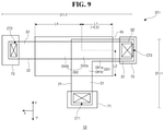
- FIG. 9 is a plan view schematically illustrating a structure of a driving TFT in a pixel region according to a fourth aspect of the present disclosure.
- a TFT substrate of aspects of the present disclosure may be applied to all sorts of electronic devices using a TFT.
- a TFT substrate may be applied to various electronic devices including a display device, a sensor panel, and the like.
- TFT substrate used for an organic light emitting display device (OLED) by way of example.
- FIG. 1 is a plan view schematically illustrating a TFT substrate of an OLED display device according to the present disclosure.
- FIG. 2 is a circuit diagram schematically illustrating a pixel region of FIG. 1 .
- the TFT 10 may include a display region AA as an active region for displaying an image, and a non-display region NA as a non-active region which is located around (or surrounds) the display region AA
- the TFT substrate 10 includes array elements to drive the OLED and may be referred to as an array substrate.
- a plurality of pixel regions P may be arranged in a matrix form.
- the plurality of pixel regions P may include, for example, red, green and blue pixel regions P respectively displaying red, green and blue.
- the red, green and blue pixel regions P may be located alternately in a direction.
- Each pixel region P may include driving elements to operate the pixel region P.
- driving elements to operate the pixel region P.
- a plurality of TFTs and a light emitting diode OP may be formed in the pixel region P.
- a driving circuit driving the pixel regions P in the display region AA may be located.
- a scan driving circuit SDC which outputs a scan signal such as a gate signal and provides the scan signal to the pixel region P may be located in the non-display region NA.
- the scan driving circuit SDC may be formed directly in the TFT substrate 10 .
- the scan driving circuit SDC formed directly in the TFT substrate 10 may be referred to as a GIP (gate in panel) type driving circuit, which may be formed in processes of manufacturing the TFT 10 .
- the GIP type scan driving circuit SDC may include a plurality of TFTs for a driving circuit, and the plurality of TFTs for the driving circuit may have a structure that is the same as or similar to that of the TFTs of the pixel region P.
- N (negative) type TFTs are used in the pixel region P by way of example.
- a plurality of TFTs for a pixel including a switching TFT STr and a driving TFT DTr and a light emitting diode OD as a light emitting element, and a storage capacitor Cst may be formed.
- the switching TFT STr may be connected to a gate line GL and a data line DL which cross each other and define the pixel region P.
- a gate electrode of the switching TFT STr may be connected to the gate line GL
- a drain electrode of the switching TFT STr may be connected to the data line DL.
- the switching TFT STr is turned on in response to a gate voltage applied through the gate line GL located at a corresponding row line, and thus a data voltage supplied through the data line DL is applied to the driving TFT DTr.
- the driving TFT DTr may be connected to the switching TFT STr and the light emitting diode OD.
- a gate electrode of the driving TFT DTr may be electrically connected to a source electrode of the switching TFT STr, and a source electrode of the driving TFT DTr may be electrically connected to the light emitting diode OD.
- a drain electrode of the driving TFT DTr may be configured to receive a first power voltage Vdd.
- the first power voltage Vdd may be a high power voltage Vdd.
- a light emitting current applied to the light emitting diode OD may be controlled according to a voltage applied to the gate electrode of the driving TFT DTr.
- the light emitting diode OD may be configured as, for example, an organic light emitting diode in which a light emission material layer is made of an organic material.
- the light emitting diode OD emits a light according to the light emitting current from the driving TFT DTr.
- the light emitting diode OD may be configured such that a first electrode thereof, for example, an anode is connected to the source electrode of the driving TFT DTr, and a second electrode thereof, for example, a cathode may be applied with a second power voltage Vss, for example, a low power voltage Vss.
- the storage capacitor Cst may be connected to the gate electrode of the driving TFT DTr and serve to maintain the voltage, which is applied to the gate electrode of the driving TFT DTr, until a next frame.
- the storage capacitor Cst may be configured such that a first electrode thereof is connected to the gate electrode of the driving TFT DTr, and a second electrode thereof is connected to, for example, the drain electrode (or the source electrode) of the driving TFT DTr.
- the driving TFT DTr may be configured with two sub-driving TFTs DTr 1 and DTr 2 which are stacked in a direction vertical to a substrate.
- the driving TFT DTr may configure to include a first sub-driving TFT DTr 1 located on the substrate, and a second sub-driving TFT DTr 2 located on the first sub-driving TFT DTr 2 .
- the first and second sub-driving TFTs DTr 1 and DTr 2 may be connected in serial to each other and share a gate electrode.
- the first sub-driving TFT DTr 1 may be applied with the first power voltage Vdd at its drain electrode, and the second sub-driving TFT DTr 2 may be connected to the light emitting diode OD at its source electrode.
- the driving TFT DTr is configured in a vertically double-stacked structure, a length of a channel of the driving TFT DTr increases in a limited area of the pixel region thus can be secured as required. Accordingly, degradation of a driving property, such as a stability of a drain current being reduced and an off current increasing because of a hot carrier reliability being deteriorated by a short length of a channel, can be improved.
- At least one sub-driving TFT may be configured such that a channel thereof is formed to extend in two directions in a plan view. Accordingly, a required length of a channel can be satisfied at a minimal area.
- a channel of at least one sub TFT may be configured to have a bent structure.
- a semiconductor layer of at least one sub TFT may be configured to have a bent structure.
- the switching TFT STr may be configured to have a single-TFT structure.
- the switching TFT STr may be formed to have a structure which is the same as or similar to that of the first or second sub-driving TFT DTr 1 or DTr 2 .
- the switching TFT STr may be configured to have a double-TFT stacked structure similar to that of the driving TFT DTr.
- At least one of TFTs formed in the scan driving circuit SDC may be configured to have a double-TFT stacked structure similar to that of the driving TFT DTr.
- FIG. 3 is a view schematically illustrating a plan structure of a driving TFT in a pixel region according to a first aspect of the present disclosure.
- FIG. 4 is a cross-sectional view taken along line IV-IV′ of FIG. 3
- FIG. 5 is a cross-sectional view taken along line V-V′ of FIG. 3 .
- the driving TFT DTr may be configured to have a structure doubly stacked in a direction vertical to a surface of a substrate 11 .
- the first sub-driving TFT DTr 1 as a lower driving TFT may be formed on the substrate 11
- the second sub-driving TFT DTr 2 as an upper driving TFT may be formed on the first sub-driving TFT DTr 1 .
- a gate electrode 45 may serve as a common gate electrode which is shared by both of the first and second sub-driving TFTs DTr 1 and DTr 2 .
- the first and second sub-driving TFTs DTr 1 and DTr 2 may be connected in series to each other.
- the cross-sectional structure of the first and second sub-driving TFTs DTr 1 and DTr 2 refers to FIG. 4 , the first sub-driving TFT DTr 1 may have a top gate structure, and the second sub-driving TFT DTr 2 may have a bottom gate structure.
- a first semiconductor layer 21 as a semiconductor layer of the first sub-driving TFT DTr may be formed on the substrate 11 .
- the first semiconductor layer 21 may be made of polycrystalline silicon.
- a buffer layer may be located below the first semiconductor layer and be formed over the entire surface of the substrate 11 .
- the first semiconductor layer 21 may include a first channel portion CH 1 which is a portion of the first semiconductor layer 21 corresponding to the gate electrode 45 thereon i.e., overlapping the gate electrode 45 , and a first source portion S 1 and a first drain portion D 1 located at both sides of the first channel portion CH 1 .
- the first source portion S 1 and the first drain portion D 1 are portions highly doped with impurities, for example, an N type or P type dopant.
- the gate electrode 45 may serve as a doping mask.
- a first gate insulating layer 31 as an insulating layer may be formed on the first semiconductor layer 21 .
- the first gate insulating layer 31 may be formed entirely over the substrate 11 .
- the first gate insulating layer 31 may be made of an inorganic insulating material, for example, silicon oxide (SiO 2 ) or silicon nitride (SiN X ).
- the gate electrode 45 corresponding to the first channel portion CH 1 may be formed on the first gate insulating layer 31 .
- the gate electrode 45 may serve as a top gate electrode for the first sub-driving TFT DTr 1 .
- a second gate insulating layer 32 as an insulating layer may be formed on the gate electrode 45 .
- the second gate insulating layer 32 may be formed entirely over the substrate 11 .
- the second gate insulating layer 32 may be made of an inorganic insulating material, for example, silicon oxide (SiO 2 ) or silicon nitride (SiN X ).
- a second semiconductor layer 22 as a semiconductor layer of the second sub-driving TFT DTr 2 may be formed on the second gate insulating layer 32 .
- the second semiconductor layer 22 may be made of polycrystalline silicon.
- the second semiconductor layer 22 may include a second channel portion CH 2 which is a portion of the second semiconductor layer 22 corresponding to the gate electrode 45 therebelow i.e., overlapping the gate electrode 45 , and a second source portion S 2 and a second drain portion D 2 located at both sides of the second channel portion CH 2 .
- the second source portion S 2 and the second drain portion D 2 are portions highly doped with impurities.
- the second source portion S 2 and the second drain portion D 2 may be doped with a dopant having the same type (N type or P type) as a dopant of the first source portion S 1 and the first drain portion D 2 .
- a photoresist pattern may be used as a doping mask.
- the gate electrode 45 is located below the second semiconductor layer 22 , the gate electrode may serve as a bottom gate electrode for the second sub-driving TFT DTr 2 .
- a passivation layer 50 as an insulating layer may be formed on the second semiconductor layer 22 .
- the passivation layer 50 may be made of an inorganic insulating material or organic insulating material.
- the passivation layer 50 may be formed to have a single-layered or multi-layered structure.
- a drain electrode 71 and a source electrode 73 may be formed on the passivation layer 50 .
- the drain electrode 71 may be connected to the first drain portion D 1 of the first sub-driving TFT DTr 1 , and the source electrode 73 may be connected to the second source portion S 2 of the second sub-driving TFT DTr 2 .
- the drain electrode 71 may be formed to contact the first drain portion D 1 .
- the second source portion S 2 of the second sub-driving TFT DTr 2 may substantially serve as a source portion of the driving TFT DTr, the source electrode 73 may be formed to contact the second source portion S 2 .
- an insulating layer therebetween for example, the passivation layer 50 and the first and second gate insulating layers 31 and 32 may have a first contact hole CT 1 formed therein. Accordingly, the first drain portion D 1 may contact the drain electrode 71 through the first contact hole CT 1 .
- the passivation layer 50 may have a second contact hole CT 2 formed therein. Accordingly, the second source portion S 2 may contact the source electrode 73 through the second contact hole CT 2 .
- first and second sub-driving TFTs DTr 1 and DTr 2 may be electrically connected in series to each other through a connection electrode 75 .
- connection electrode 75 may be formed of the same metal material as and in the same process as the drain and source electrodes 71 and 73 .
- connection electrode 75 may contact the first source portion S 1 and the drain portion D 2 , which are located below the connection electrode 75 , through a third contact hole CT 3 .
- the third contact hole CT 3 may be formed in the passivation layer 50 and the first and second gate insulating layers 31 and 32 , and further formed in the second drain portion D 2 . In other words, the third contact hole CT 3 may be formed to penetrate the second drain portion D 2 .
- connection electrode 75 may contact an inner surface of the second drain portion D 2 (i.e., an inner surface exposed by (or surrounding or defining) the third contact hole CT 3 ), and contact a top surface of the first source portion S 1 .
- the first source portion S 1 may be formed to have the third contact hole CT 3 therein similarly to the second drain portion D 2 , and in this case, the connection electrode 75 may contact an inner surface of the first source portion S 1 exposed by the third contact hole CT 3 .
- the first source portion S 1 and the second drain portion D 2 which overlap and are located below the connection electrode 75 , may be electrically connected through the connection electrode 75 , and thus the first and second sub-driving TFTs DTr 1 and DTr 2 (or the first and second semiconductor layers 21 and 22 ) may be connected in series.
- connection electrode 75 made of a metal material, a stable electrical connection between the first and second sub-driving TFTs DTr 1 and DTr 2 can be made.
- a method of connecting the second drain portion D 2 directly to the first source portion S 1 through a contact hole without the connection electrode 75 might be considered.
- the second drain portion D 2 has a great resistance because of its material characteristics, and thus a connection resistance between the first and second sub-driving TFTs DTr 1 and DTr 2 increases.
- connection electrode 75 made of a metal material since the connection electrode 75 made of a metal material is used, a connection resistance between the first and second sub-driving TFTs DTr 1 and DTr 2 is reduced, and a stable electrical connection can be made.
- the driving TFT DTr is configured in a vertically double-stacked structure that the first and second semiconductor layers 21 and 22 are arranged with the gate electrode 45 located on the first semiconductor layer 21 and below the second semiconductor layer 22 . Accordingly, the double channel portions CH 1 and CH 2 overlapping each other in the vertical direction to the substrate 11 are formed, and thus a length of a channel can increase by at least two times compared with the prior art single-stacked structure using a single semiconductor.
- first and second semiconductor layers 21 and 22 may be formed to have a bent structure in a plan view, and the first and second channel portions CH 1 and CH 2 thereof may have a bent structure in a plan view. Accordingly, a length of a channel can be secured as much as possible in a limited area.
- the first semiconductor layer 21 may include a first part which extends in a first direction, for example, an x direction, and a second part which is bent from the first part and extends in a second direction, different from the first direction, for example, a ⁇ y direction.
- the first semiconductor layer 21 may be formed to have a bent structure in a plan view.
- the first channel portion CH 1 may include a first channel part CH 1 a which extends in the first direction as the x direction, and a second channel part CH 1 b which is bent from the first channel part CH 1 a and extends in the second direction as the ⁇ y direction.
- the first channel portion CH 1 may include a first channel length L 1 as a length of a channel in the first direction defined by the first channel part CH 1 a , and a second channel length L 2 as a length of a channel in the second direction defined by the second channel part CH 1 b .
- the first channel portion CH 1 may have a channel length, L 1 +L 2 .
- the second semiconductor layer 22 may include a third part which extends in the first direction as the x direction and overlaps the first part of the first semiconductor layer 21 , and a fourth part which is bent from the third part and extends in a third direction, different from the first direction and the second direction, for example, a y direction (or +y direction).
- the second semiconductor layer 22 may be formed to have a bent structure in a plan view.
- the second channel portion CH 2 may include a third channel part CH 2 a which extends in the first direction as the x direction and overlaps the first channel part CH 1 a , and a fourth channel part CH 2 b which is bent from the third channel part CH 2 a and extends in the third direction as the +y direction.
- the third channel part CH 2 a of the second channel portion CH 2 may extend in the first direction that is the same direction as the first channel part CH 1 a of the first channel portion CH 1 , and may overlap the first channel part CH 1 a at the same length.
- the second channel portion CH 2 may include the third channel length L 3 as a length of a channel in the first direction defined by the third channel part CH 2 a , and a fourth channel length L 4 as a length of a channel in the third direction defined by the fourth channel part CH 2 b .
- the first and second semiconductor layers 21 and 22 and their first and second channel portions CH 1 and CH 2 may have the bent structure, and the bent direction of the first channel portion CH 1 and the bent direction of the second channel portion CH 2 may be different, for example, opposite to each other.
- the first and second channel portions CH 1 and CH 2 are configured to be arranged in a vertically stacked structure with the gate electrode 45 therebetween and to have a bent structure in plane, and thus a channel length with respect to an occupied area can be maximized.
- a channel length of the driving TFT DTr to achieve a required driving property at a minimal area can be secured, and an area availability for the pixel region P can be improved.
- the driving TFT DTr securing a stable driving property can be provided effectively in a limited pixel region P.
- first channel portion CH 1 and the second channel portion CH 2 are configured to be bent and extend in the different directions (e.g., the ⁇ y direction and the +y direction, respectively), the channel lengths in the different directions can be adjusted individually, and thus the channel length of the first channel portion CH 1 and the channel length of the second channel portion CH 2 can be adjusted freely as required.
- the channel length, in the second direction as the ⁇ y direction, of the first channel portion CH 1 , and the channel length, in the third direction as the +y direction, of the second channel portion CH 2 may be equal or different.
- the first and second sub-driving TFTs DTr 1 and DTr 2 may be formed in a symmetrical or unsymmetrical form.
- the channel length of the first channel portion CH 1 and the channel length of the second channel portion CH 2 may be adjusted individually by making the first and second channel portions CH 1 and CH 2 bent in different directions. Accordingly, various driving properties respectively required for the first and second sub-driving TFTs DTr 1 and DTr 2 can be satisfied, and thus the driving TFT DTr suitable for a required property can be provided effectively.
- FIG. 6 is a cross-sectional view schematically illustrating a structure of a driving TFT in a pixel region according to a second aspect of the present disclosure.
- a driving TFT DTr of this aspect may be an N type TFT and use an LDD (lightly doped drain) TFT.
- a first semiconductor layer 21 of a first sub-driving TFT DTr 1 may include a first lightly doped drain (LDD) portion LDD 1 which is located between a first channel portion CH 1 and a first source portion S 1 , and between the first channel portion CH 1 and a first drain portion D 1 .
- LDD lightly doped drain
- a second semiconductor layer 22 of a second sub-driving TFT DTr 2 may include a second LDD portion LDD 2 which is located between a second channel portion CH 2 and a second source portion S 2 , and between the second channel portion CH 2 and a second drain portion D 2 .
- sizes i.e., lengths of the first LDD portion LDD 1 and the second LDD portions LDD 2 may be adjusted individually.
- a first length LL 1 of the first LDD portion LDD 1 and a second length LL 2 of the second LDD portion LDD 2 may be equal or different.
- first channel portion CH 1 and the second channel portion CH 2 are bent in different directions (e.g., the ⁇ y direction and the +y direction, respectively), an end of the first channel portion CH 1 and an end of the second channel portion CH 2 are spaced apart from and separated from each other.
- an end, at a drain side, of the first channel portion CH 1 , and an end, at a source side, of the second channel portion CH 2 are spaced apart from and separated from each other.
- the first LDD portion LDD 1 at the drain side, of the first channel portion CH 1 is not substantially affected by a doping process for the second semiconductor layer 22 located over the first semiconductor layer 21 .
- the first length LL 1 of the first LDD portion LDD 1 and the second length LL 2 of the second LDD portion LDD 2 may be adjusted individually.
- the optimal LDD portions respectively required for the first and second sub-driving TFTs DTr 1 and DTr 2 can be formed, and thus the driving TFT DTr suitable for a required property can be provided effectively.
- FIGS. 7 and 8 are a plan view and a cross sectional view, respectively, schematically illustrating a structure of a driving TFT in a pixel region according to a third aspect of the present disclosure.
- a driving TFT DTr of this aspect may include an electrode pattern 60 which is located on a second sub-driving TFT DTr 2 , and corresponds to and overlaps a second channel portion CH 2 of the second sub-driving TFT DTr 2 .
- a first passivation layer 51 may be formed on a second semiconductor layer 22 , and the electrode pattern 60 may be formed on the first passivation layer 51 .
- a second passivation layer 52 may be formed on the electrode pattern 60 , and a drain electrode 71 and a source electrode 73 may be formed on the second passivation layer 52 .
- the electrode pattern 60 may be arranged to correspond to and overlap the second channel pattern CH 2 , and may serve as a doping mask in a doping process for a second source portion S 2 and a second drain portion D 2 of the second semiconductor layer 22 .
- the electrode pattern 60 may serve to block a light traveling toward the second channel portion CH 2 from the outside over the electrode pattern 60 . Further, the electrode pattern 60 may overlap at least part of the first channel portion CH 1 .
- the electrode pattern 60 may serve as a back gate electrode.
- the electrode pattern 60 may be supplied with an individual bias voltage from a power supply circuit, or may be electrically connected to the gate electrode 45 .
- the electrode pattern 60 may be electrically connected to the source electrode 73 .
- the electrode pattern 60 may be electrically connected to the drain electrode 71 so that the electrode pattern 60 serves as one electrode of a storage capacitor (Cst of FIG. 2 ) i.e., a storage electrode facing the gate electrode 45 .
- a storage capacitor Cst of FIG. 2
- FIG. 9 is a plan view schematically illustrating a structure of a driving TFT in a pixel region according to a fourth aspect of the present disclosure.
- one of first and second sub-driving TFTs DTr 1 and DTr 2 may have a bent structure, and the other of first and second sub-driving TFTs DTr 1 and DTr 2 may have a non-bent structure i.e., a linear structure.
- the first sub-driving TFT DTr 1 has the bent structure
- the second sub-driving TFT DTr 2 has the linear structure
- a second semiconductor layer 22 of the second sub-driving TFT DTr 2 may include a third part that extends in a first direction as a x direction and overlaps the first semiconductor layer 21 , and a fourth part that continuously extends (or further extends) from the third part in the first direction.
- a second channel portion CH 2 of the second semiconductor layer 22 may be formed to have the linear structure.
- the second channel portion CH 2 may include a third part CH 2 a that extends in a first direction as a x direction and overlaps a first channel portion CH 1 , and a fourth part CH 2 b that continuously extends from the third part CH 2 a in the first direction.
- the third channel part CH 2 a of the second channel portion CH 2 may extend in the first direction that is the same direction as a first channel part CH 1 a of the first channel portion CH 1 , and may overlap the first channel part CH 1 a at the same length.
- the third channel part CH 2 a may have substantially the same channel length as the first channel part CH 1 a.
- the fourth channel part CH 2 b of the second channel portion CH 2 extends continuously in the first direction that is different from an extension direction of a second channel part CH 1 b of the first channel portion CH 1 , and has a fourth channel length L 4 .
- the first semiconductor layer 21 and its first channel portion CH 1 may have the bent structure in a plane view
- the second semiconductor layer 22 and its second channel portion CH 2 may have the linear structure in a plane view.
- bent and linear hybrid structure of the fourth aspect, and the bent structure of the first aspect may be properly selected depending on arrangement of elements of the pixel region P and the like.
- a channel length with respect to an occupied area can increase.
- a channel length of the driving TFT DTr to achieve a required driving property at a minimal area can be secured, and an area availability for the pixel region P can be improved.
- first and second channel portions CH 1 and CH 2 may respectively have the channel parts that are the second channel part CH 1 b and the fourth channel part CH 2 b extending in different directions, and the channel length of the first channel portion CH 1 and the channel length of the second channel portion CH 2 may be adjusted individually. Accordingly, various driving properties respectively required for the first and second sub-driving TFTs DTr 1 and DTr 2 can be satisfied, and thus the driving TFT DTr suitable for a required property can be provided effectively.
- the driving TFT is configured to have a vertically double-stacked structure sharing the gate electrode, and at least one channel portion of the driving TFT has a bent structure.
- a channel length of the driving TFT with respect to an occupied area can increase. Therefore, a channel length of the driving TFT DTr to achieve a required driving property at a minimal area can be secured, and a stable driving property can be achieved. Further, an area availability for the pixel region can be improved.
- the two channel portions vertically stacked have the respective channel parts extending in different directions, and their channel lengths can be adjusted individually. Therefore, various driving properties respectively required for the two sub-driving TFTs can be satisfied, and thus the driving TFT suitable for a required property can be provided effectively.
Landscapes
- Engineering & Computer Science (AREA)
- Microelectronics & Electronic Packaging (AREA)
- Power Engineering (AREA)
- Physics & Mathematics (AREA)
- Condensed Matter Physics & Semiconductors (AREA)
- General Physics & Mathematics (AREA)
- Computer Hardware Design (AREA)
- Ceramic Engineering (AREA)
- Chemical & Material Sciences (AREA)
- Crystallography & Structural Chemistry (AREA)
- Geometry (AREA)
- Optics & Photonics (AREA)
- Devices For Indicating Variable Information By Combining Individual Elements (AREA)
- Electroluminescent Light Sources (AREA)
- Thin Film Transistor (AREA)
Priority Applications (1)
| Application Number | Priority Date | Filing Date | Title |
|---|---|---|---|
| US17/562,641 US11908951B2 (en) | 2018-09-13 | 2021-12-27 | TFT substrate and light emitting display device including the same |
Applications Claiming Priority (2)
| Application Number | Priority Date | Filing Date | Title |
|---|---|---|---|
| KR10-2018-0109344 | 2018-09-13 | ||
| KR1020180109344A KR20200030751A (ko) | 2018-09-13 | 2018-09-13 | Tft 기판 및 이를 포함한 발광표시장치 |
Related Child Applications (1)
| Application Number | Title | Priority Date | Filing Date |
|---|---|---|---|
| US17/562,641 Division US11908951B2 (en) | 2018-09-13 | 2021-12-27 | TFT substrate and light emitting display device including the same |
Publications (2)
| Publication Number | Publication Date |
|---|---|
| US20200091350A1 US20200091350A1 (en) | 2020-03-19 |
| US11245041B2 true US11245041B2 (en) | 2022-02-08 |
Family
ID=69773135
Family Applications (2)
| Application Number | Title | Priority Date | Filing Date |
|---|---|---|---|
| US16/555,753 Active 2039-12-21 US11245041B2 (en) | 2018-09-13 | 2019-08-29 | TFT substrate and light emitting display device including the same |
| US17/562,641 Active 2040-01-04 US11908951B2 (en) | 2018-09-13 | 2021-12-27 | TFT substrate and light emitting display device including the same |
Family Applications After (1)
| Application Number | Title | Priority Date | Filing Date |
|---|---|---|---|
| US17/562,641 Active 2040-01-04 US11908951B2 (en) | 2018-09-13 | 2021-12-27 | TFT substrate and light emitting display device including the same |
Country Status (3)
| Country | Link |
|---|---|
| US (2) | US11245041B2 (zh) |
| KR (1) | KR20200030751A (zh) |
| CN (1) | CN110896090A (zh) |
Cited By (1)
| Publication number | Priority date | Publication date | Assignee | Title |
|---|---|---|---|---|
| US20230186841A1 (en) * | 2021-03-16 | 2023-06-15 | Shanghai Tianma Micro-electronics Co., Ltd. | Display panel and display device |
Families Citing this family (1)
| Publication number | Priority date | Publication date | Assignee | Title |
|---|---|---|---|---|
| CN114793474A (zh) * | 2020-11-26 | 2022-07-26 | 京东方科技集团股份有限公司 | 显示基板及其制作方法、显示装置 |
Citations (2)
| Publication number | Priority date | Publication date | Assignee | Title |
|---|---|---|---|---|
| US20160189611A1 (en) * | 2013-09-12 | 2016-06-30 | Sony Corporation | Display device, method of manufacturing the same, and electronic apparatus |
| KR20170124523A (ko) | 2016-04-01 | 2017-11-10 | 보에 테크놀로지 그룹 컴퍼니 리미티드 | Tft 어레이 기판, 그 제조 방법, 및 디스플레이 디바이스 |
Family Cites Families (7)
| Publication number | Priority date | Publication date | Assignee | Title |
|---|---|---|---|---|
| KR101337134B1 (ko) * | 2006-12-13 | 2013-12-05 | 엘지디스플레이 주식회사 | 박막 트랜지스터, 박막 트랜지스터를 포함하는 평판 표시장치 및 평판 표시 장치의 제조 방법 |
| US8049253B2 (en) * | 2007-07-11 | 2011-11-01 | Semiconductor Energy Laboratory Co., Ltd. | Semiconductor device and method for manufacturing the same |
| US8878176B2 (en) | 2011-08-11 | 2014-11-04 | The Hong Kong University Of Science And Technology | Metal-oxide based thin-film transistors with fluorinated active layer |
| TW201338102A (zh) * | 2012-03-14 | 2013-09-16 | Wintek Corp | 主動元件及主動元件陣列基板 |
| KR102623624B1 (ko) | 2016-05-18 | 2024-01-10 | 삼성디스플레이 주식회사 | 트랜지스터 표시판 및 그 제조 방법 |
| KR20180024909A (ko) | 2016-08-31 | 2018-03-08 | 엘지디스플레이 주식회사 | 구동 트랜지스터와 이를 구비한 유기 발광 다이오드 표시 장치 및 그들의 제조 방법 |
| KR20180079036A (ko) | 2016-12-30 | 2018-07-10 | 엘지디스플레이 주식회사 | 구동 박막 트랜지스터 및 이를 이용한 유기 발광 표시 장치 |
-
2018
- 2018-09-13 KR KR1020180109344A patent/KR20200030751A/ko not_active Application Discontinuation
-
2019
- 2019-08-29 US US16/555,753 patent/US11245041B2/en active Active
- 2019-09-05 CN CN201910837242.9A patent/CN110896090A/zh active Pending
-
2021
- 2021-12-27 US US17/562,641 patent/US11908951B2/en active Active
Patent Citations (2)
| Publication number | Priority date | Publication date | Assignee | Title |
|---|---|---|---|---|
| US20160189611A1 (en) * | 2013-09-12 | 2016-06-30 | Sony Corporation | Display device, method of manufacturing the same, and electronic apparatus |
| KR20170124523A (ko) | 2016-04-01 | 2017-11-10 | 보에 테크놀로지 그룹 컴퍼니 리미티드 | Tft 어레이 기판, 그 제조 방법, 및 디스플레이 디바이스 |
Cited By (4)
| Publication number | Priority date | Publication date | Assignee | Title |
|---|---|---|---|---|
| US20230186841A1 (en) * | 2021-03-16 | 2023-06-15 | Shanghai Tianma Micro-electronics Co., Ltd. | Display panel and display device |
| US20230186839A1 (en) * | 2021-03-16 | 2023-06-15 | Shanghai Tianma Micro-electronics Co., Ltd. | Display panel and display device |
| US20230186840A1 (en) * | 2021-03-16 | 2023-06-15 | Shanghai Tianma Micro-electronics Co., Ltd. | Display panel and display device |
| US11915638B2 (en) * | 2021-03-16 | 2024-02-27 | Shanghai Tianma Micro-electronics Co., Ltd. | Display panel and display device |
Also Published As
| Publication number | Publication date |
|---|---|
| US11908951B2 (en) | 2024-02-20 |
| US20200091350A1 (en) | 2020-03-19 |
| KR20200030751A (ko) | 2020-03-23 |
| US20220123153A1 (en) | 2022-04-21 |
| CN110896090A (zh) | 2020-03-20 |
Similar Documents
| Publication | Publication Date | Title |
|---|---|---|
| US10854705B2 (en) | Display apparatus and method of manufacturing display apparatus | |
| US9053986B2 (en) | Semiconductor device and flat panel display including the same | |
| US7348655B2 (en) | Organic electro luminescence device and fabrication method thereof | |
| US11908951B2 (en) | TFT substrate and light emitting display device including the same | |
| KR101968666B1 (ko) | 유기 발광 표시 장치 및 그 제조 방법 | |
| US6930331B2 (en) | Thin film transistor for use in active matrix type organic light emitting diode device | |
| US20080157081A1 (en) | Organic light emitting device and method for manufacturing the same | |
| US7470950B2 (en) | Thin film transistor substrate and display apparatus having the same | |
| US11764254B2 (en) | Display apparatus | |
| US7671366B2 (en) | Thin film transistor and organic light emitting device including thin film transistor | |
| US8013523B2 (en) | Organic light emitting device and manufacturing method thereof | |
| US20170141175A1 (en) | Display device and a manufacturing method thereof | |
| KR100689913B1 (ko) | 액티브 매트릭스형 표시 장치 | |
| CN113903751A (zh) | 薄膜晶体管阵列衬底和显示器件 | |
| US20060102902A1 (en) | Thin film transistor array panel | |
| US20230163137A1 (en) | Driving thin film transistor and display device including the same | |
| CN111383572A (zh) | 具有由四个子像素构成的单位像素的显示装置 | |
| CN219513108U (zh) | 显示装置 | |
| US20240144878A1 (en) | Display substrate and display apparatus | |
| CN115968231A (zh) | 显示面板和显示装置 | |
| CN115223446A (zh) | 显示装置 | |
| CN115720671A (zh) | 显示基板和显示装置 | |
| KR20190040160A (ko) | 유기 발광 표시 장치 및 그 제조 방법 |
Legal Events
| Date | Code | Title | Description |
|---|---|---|---|
| AS | Assignment |
Owner name: LG DISPLAY CO., LTD., KOREA, REPUBLIC OF Free format text: ASSIGNMENT OF ASSIGNORS INTEREST;ASSIGNOR:OH, KUM-MI;REEL/FRAME:050216/0117 Effective date: 20190722 |
|
| FEPP | Fee payment procedure |
Free format text: ENTITY STATUS SET TO UNDISCOUNTED (ORIGINAL EVENT CODE: BIG.); ENTITY STATUS OF PATENT OWNER: LARGE ENTITY |
|
| STPP | Information on status: patent application and granting procedure in general |
Free format text: NON FINAL ACTION MAILED |
|
| STPP | Information on status: patent application and granting procedure in general |
Free format text: RESPONSE TO NON-FINAL OFFICE ACTION ENTERED AND FORWARDED TO EXAMINER |
|
| STPP | Information on status: patent application and granting procedure in general |
Free format text: NOTICE OF ALLOWANCE MAILED -- APPLICATION RECEIVED IN OFFICE OF PUBLICATIONS |
|
| STPP | Information on status: patent application and granting procedure in general |
Free format text: PUBLICATIONS -- ISSUE FEE PAYMENT VERIFIED |
|
| STCF | Information on status: patent grant |
Free format text: PATENTED CASE |