US10943170B2 - Neural network circuit - Google Patents
Neural network circuit Download PDFInfo
- Publication number
- US10943170B2 US10943170B2 US16/249,190 US201916249190A US10943170B2 US 10943170 B2 US10943170 B2 US 10943170B2 US 201916249190 A US201916249190 A US 201916249190A US 10943170 B2 US10943170 B2 US 10943170B2
- Authority
- US
- United States
- Prior art keywords
- voltage
- selection element
- line connected
- ref
- expressed
- Prior art date
- Legal status (The legal status is an assumption and is not a legal conclusion. Google has not performed a legal analysis and makes no representation as to the accuracy of the status listed.)
- Active, expires
Links
- 238000013528 artificial neural network Methods 0.000 title claims abstract description 21
- 230000003321 amplification Effects 0.000 claims abstract description 5
- 238000006243 chemical reaction Methods 0.000 claims abstract description 5
- 238000003199 nucleic acid amplification method Methods 0.000 claims abstract description 5
- 230000000052 comparative effect Effects 0.000 description 13
- 238000010586 diagram Methods 0.000 description 8
- XBGNERSKEKDZDS-UHFFFAOYSA-N n-[2-(dimethylamino)ethyl]acridine-4-carboxamide Chemical compound C1=CC=C2N=C3C(C(=O)NCCN(C)C)=CC=CC3=CC2=C1 XBGNERSKEKDZDS-UHFFFAOYSA-N 0.000 description 8
- 238000000034 method Methods 0.000 description 3
- 210000000225 synapse Anatomy 0.000 description 3
- 230000008901 benefit Effects 0.000 description 2
- 230000008569 process Effects 0.000 description 2
- 230000004913 activation Effects 0.000 description 1
- 239000002131 composite material Substances 0.000 description 1
- 230000006870 function Effects 0.000 description 1
- 238000012986 modification Methods 0.000 description 1
- 230000004048 modification Effects 0.000 description 1
- 210000002569 neuron Anatomy 0.000 description 1
Images


Classifications
-
- G06N3/0635—
-
- G—PHYSICS
- G11—INFORMATION STORAGE
- G11C—STATIC STORES
- G11C11/00—Digital stores characterised by the use of particular electric or magnetic storage elements; Storage elements therefor
- G11C11/54—Digital stores characterised by the use of particular electric or magnetic storage elements; Storage elements therefor using elements simulating biological cells, e.g. neuron
-
- G—PHYSICS
- G06—COMPUTING; CALCULATING OR COUNTING
- G06N—COMPUTING ARRANGEMENTS BASED ON SPECIFIC COMPUTATIONAL MODELS
- G06N3/00—Computing arrangements based on biological models
- G06N3/02—Neural networks
- G06N3/06—Physical realisation, i.e. hardware implementation of neural networks, neurons or parts of neurons
- G06N3/063—Physical realisation, i.e. hardware implementation of neural networks, neurons or parts of neurons using electronic means
- G06N3/065—Analogue means
-
- G—PHYSICS
- G11—INFORMATION STORAGE
- G11C—STATIC STORES
- G11C13/00—Digital stores characterised by the use of storage elements not covered by groups G11C11/00, G11C23/00, or G11C25/00
- G11C13/0002—Digital stores characterised by the use of storage elements not covered by groups G11C11/00, G11C23/00, or G11C25/00 using resistive RAM [RRAM] elements
- G11C13/0021—Auxiliary circuits
- G11C13/004—Reading or sensing circuits or methods
-
- G—PHYSICS
- G11—INFORMATION STORAGE
- G11C—STATIC STORES
- G11C13/00—Digital stores characterised by the use of storage elements not covered by groups G11C11/00, G11C23/00, or G11C25/00
- G11C13/0002—Digital stores characterised by the use of storage elements not covered by groups G11C11/00, G11C23/00, or G11C25/00 using resistive RAM [RRAM] elements
- G11C13/0021—Auxiliary circuits
- G11C13/0069—Writing or programming circuits or methods
-
- G—PHYSICS
- G11—INFORMATION STORAGE
- G11C—STATIC STORES
- G11C13/00—Digital stores characterised by the use of storage elements not covered by groups G11C11/00, G11C23/00, or G11C25/00
- G11C13/0002—Digital stores characterised by the use of storage elements not covered by groups G11C11/00, G11C23/00, or G11C25/00 using resistive RAM [RRAM] elements
- G11C13/0021—Auxiliary circuits
- G11C13/0097—Erasing, e.g. resetting, circuits or methods
-
- G—PHYSICS
- G11—INFORMATION STORAGE
- G11C—STATIC STORES
- G11C13/00—Digital stores characterised by the use of storage elements not covered by groups G11C11/00, G11C23/00, or G11C25/00
- G11C13/0002—Digital stores characterised by the use of storage elements not covered by groups G11C11/00, G11C23/00, or G11C25/00 using resistive RAM [RRAM] elements
- G11C13/0007—Digital stores characterised by the use of storage elements not covered by groups G11C11/00, G11C23/00, or G11C25/00 using resistive RAM [RRAM] elements comprising metal oxide memory material, e.g. perovskites
-
- G—PHYSICS
- G11—INFORMATION STORAGE
- G11C—STATIC STORES
- G11C13/00—Digital stores characterised by the use of storage elements not covered by groups G11C11/00, G11C23/00, or G11C25/00
- G11C13/0002—Digital stores characterised by the use of storage elements not covered by groups G11C11/00, G11C23/00, or G11C25/00 using resistive RAM [RRAM] elements
- G11C13/0021—Auxiliary circuits
- G11C13/004—Reading or sensing circuits or methods
- G11C2013/005—Read using potential difference applied between cell electrodes
-
- G—PHYSICS
- G11—INFORMATION STORAGE
- G11C—STATIC STORES
- G11C13/00—Digital stores characterised by the use of storage elements not covered by groups G11C11/00, G11C23/00, or G11C25/00
- G11C13/0002—Digital stores characterised by the use of storage elements not covered by groups G11C11/00, G11C23/00, or G11C25/00 using resistive RAM [RRAM] elements
- G11C13/0021—Auxiliary circuits
- G11C13/0069—Writing or programming circuits or methods
- G11C2013/0073—Write using bi-directional cell biasing
-
- G—PHYSICS
- G11—INFORMATION STORAGE
- G11C—STATIC STORES
- G11C13/00—Digital stores characterised by the use of storage elements not covered by groups G11C11/00, G11C23/00, or G11C25/00
- G11C13/0002—Digital stores characterised by the use of storage elements not covered by groups G11C11/00, G11C23/00, or G11C25/00 using resistive RAM [RRAM] elements
- G11C13/0021—Auxiliary circuits
- G11C13/0069—Writing or programming circuits or methods
- G11C2013/0088—Write with the simultaneous writing of a plurality of cells
-
- G—PHYSICS
- G11—INFORMATION STORAGE
- G11C—STATIC STORES
- G11C13/00—Digital stores characterised by the use of storage elements not covered by groups G11C11/00, G11C23/00, or G11C25/00
- G11C13/0002—Digital stores characterised by the use of storage elements not covered by groups G11C11/00, G11C23/00, or G11C25/00 using resistive RAM [RRAM] elements
- G11C13/0021—Auxiliary circuits
- G11C13/0069—Writing or programming circuits or methods
- G11C2013/009—Write using potential difference applied between cell electrodes
-
- G—PHYSICS
- G11—INFORMATION STORAGE
- G11C—STATIC STORES
- G11C2213/00—Indexing scheme relating to G11C13/00 for features not covered by this group
- G11C2213/70—Resistive array aspects
- G11C2213/77—Array wherein the memory element being directly connected to the bit lines and word lines without any access device being used
Definitions
- the present disclosure relates to a neural network circuit.
- a neural network circuit includes an element having two terminals as a synapse, the element being nonvolatile and capable of varying a conductance value and being referred to as a memristor.
- the present disclosure provides a neural network circuit including: a storage part that includes memristors connected in a lattice shape; a voltage application circuit; and a controller.
- the voltage application circuit is configured to apply a bias voltage to the storage part.
- the controller is configured to control the voltage application circuit to perform to the selection element, at least one of writing, erasing, or reading of the data.
- the controller varies the bias voltage applied through the voltage application circuit.
- FIG. 1 is a view illustrating a state of applying of a bias voltage to perform writing in a selection element of memristors
- FIG. 2 is a view illustrating a state of the applying of a bias voltage to perform erasing of the selection element
- FIG. 3 is a view illustrating a state of the applying of a bias voltage to perform reading from the selection element
- FIG. 4 is a functional block diagram showing a configuration of a neural network circuit
- FIG. 5 is a view illustrating an on/off state of each switch at the applying of the bias voltage to perform the writing in the selection element
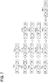
- FIG. 6 is a diagram showing characteristics of a DAC having polarity bits
- FIG. 7 is a diagram showing a generation state of data input to each DAC
- FIG. 8 is a diagram showing a generation state of data input to each DAC at the erasing of the selected element
- FIG. 9 is a view illustrating an on/off state of each switch at the applying of the bias voltage to perform the reading from the selected element
- FIG. 10 is a diagram showing a first comparative example
- FIG. 11 is a diagram showing a second comparative example
- FIG. 12 is a diagram showing a third comparative example.
- FIG. 13 is a diagram showing a fourth comparative example.
- a neural network circuit includes a two-terminal element as a synapse, the two-terminal element being nonvolatile and capable of varying a conductance value.
- the two-terminal element is called as a memristor.
- the memristor is arranged in a lattice shape.
- a voltage is applied to the memristor, and a current is generated.
- a composite current is converted into a voltage by a transimpedance amplifier.
- a waveform of the voltage is shaped by an activation function.
- the voltage is output as a voltage value.
- the memristor operates as a synapse, and the transimpedance amplifier operates as a neuron.
- the transimpedance amplifier performs a product-sum operation of the conductance value of the memristor with the applied voltage.
- an erasing voltage is applied to both ends of the memristor.
- a reading voltage is applied to the memristor.
- the current value is read.
- a writing voltage is applied to the memristor.
- the memristor including the switch or the selector When the voltage is applied in a case of employing the memristor including the switch or the selector, it may be possible to arbitrarily set an accurate conductance value. However, when the memristor that does not include the switch and the selector is arranged in the lattice shape, “disturbance” affects the conductance value of the unselection element (also referred to as a non-selection element). For example, a bias method is proposed as shown in FIG. 12 corresponding to a third comparative example and FIG. 13 corresponding to a fourth comparative example.
- a voltage V is applied to both ends of the selection element
- a voltage V/2 and a voltage V/3 are applied to the unselection element.
- the selection target corresponds to a memristor targeted for the writing, the reading, or the erasing.
- the unselection element corresponds to a memristor untargeted for the writing, the reading, or the erasing.
- a ReRAM resistive random access memory, registered trademark
- FIG. 1 to FIG. 3 show a 3 ⁇ 3 memristor array also called a crossbar as one example.
- Lines R 1 to R 3 aligned in a row direction and lines C 1 to C 3 aligned in a column direction are arranged so as to cross each other.
- Memristors G 11 to G 33 as a memory element (also referred to as a storage element) are arranged corresponding to lattice points at which two of the lines cross.
- a first end (also referred to as one end) of each of memristors G 11 to G 33 is connected with each of the lines C 1 to C 3 .
- a second end (also referred to as the other end) of each of the memristors G 11 to G 33 is connected with each of the lines R 1 to R 3 .
- a side of a line C may be referred to as a first end side
- a side of a line R may be referred to as a second end side.
- the memristor employed in the embodiment is a variable resistance element having the bipolar characteristics.
- the voltages are applied to the lines C 2 and C 3 , R 2 and R 3 other than the line C 1 and the line R 1 , respectively, as following:
- Lines R 2 and R 3 V REF +V SET /4.
- the first ends of the memristors corresponding to unselection elements G 12 and G 13 are commonly connected with the memristor G 11 through the line C 1 .
- a voltage V SET /4 is applied to both ends of the memristors G 12 and G 13 corresponding to the unselection elements.
- the second ends of the memristor corresponding to the unselection elements G 21 and G 31 are commonly connected with the memristor G 11 through the line R 1 .
- the voltage W SET /4 is applied to both ends of the memristors G 21 and G 31 corresponding to the unselection elements.
- a voltage ⁇ V SET /2 is applied to both ends of the memristor G 22 , G 23 , G 32 , and G 33 , which are the other unselection elements.
- the bias voltage V SET /4 applied to a part of the unselection elements becomes lower than the bias voltages of the third comparative example and the fourth comparative example. Therefore, it may be possible to further reduce the influence of disturbance (also referred to as disturb).
- the bias voltage ⁇ V SET /2 applied to a part of the other unselection elements becomes an inversion bias. Therefore, it may be possible to ignore the influence of the disturbance.
- a detailed theory is described in a non-patent literature (“Phenomenological Modeling of Memristic Devices” Applied Physics A, vol. 118, pp. 770-786, 2015).
- an erasing voltage V RESET at the inversion bias is applied to both ends of the memristor G 11 when erasing and resetting the memristor G 11 corresponding to the selection element. Therefore, voltages are applied to the lines C 1 and R 1 , respectively as following:
- the “bias voltage” ⁇ V RESET /2 is applied to both ends of the memristors G 12 , G 13 , G 21 , and G 31 corresponding to the unselection elements. Since the bias voltage ⁇ V RESET /2 is inversion bias, it may be possible to ignore the influence of the disturbance. The bias voltage is not applied to both ends of the other memristor G 22 , G 23 , G 32 , and G 33 corresponding to the unselection elements. Therefore, the disturbance does not occur.
- a reading voltage V READ at the inversion bias is applied to both ends of the memristor G 11 when reading the memristor G 11 as the selection element. Therefore, the voltage is applied to the line C 1 as following;
- the reference voltage V REF is applied to the other lines C 2 and C 3 , R 1 to R 3 , respectively.
- a neural network circuit 1 includes a crossbar 2 having the memristor arranged in a lattice shape as a storage part, similarly to FIG. 1 .
- a DAC 3 that is a D/A converter outputs analog voltages corresponding to data input from a writing control circuit 4 . The voltages are applied to the lines R and C of the crossbar 2 .
- the DAC 3 corresponds to a voltage applying part or a voltage application circuit.
- the writing control part corresponds to a controller.
- the line R of the crossbar 2 is connected with an input terminal of a transimpedance amplifier 5 .
- the transimpedance amplifier 5 converts current flowing through the line R of the crossbar 2 into a voltage in performing the reading.
- the transimpedance amplifier 5 inputs the voltage to an ADC 6 that is an A/D converter.
- the ADC 6 converts an input voltage into digital data, and inputs the digital data to the writing control circuit 4 .
- the transimpedance amplifier 5 corresponds to an I/V conversion amplification circuit or a conversion amplification circuit.
- the writing control circuit 4 is connected with a microcomputer 7 (or an external control circuit 7 ) outside the neural network circuit 1 .
- the microcomputer 7 inputs an address and the conductance value of the crossbar 2 to the writing control circuit 4 in order to control the bias voltage applied to the crossbar 2 .
- the writing control circuit 4 inputs the data of the applying voltage corresponding to the address to the DAC 3 .
- the writing control circuit 4 transmits the control signal corresponding to the address to the transimpedance amplifier 5 .
- the writing control circuit 4 does not operate the ADC 6 in performing the writing of the data and the erasing of the data.
- the writing control circuit 4 operates the ADC 6 corresponding to the address only in performing the reading.
- the writing control circuit 4 reads the data.
- the writing control circuit 4 compares the read data of the ADC 6 with the conductance value input from the microcomputer 7 .
- the writing control circuit 4 performs the writing, the erasing, and the reading again.
- the writing control circuit 4 increases the erasing voltage V RSET , and performs the writing, the erasing, and the reading again.
- the writing control circuit 4 inverts an error output flag input to the microcomputer 7 .
- the microcomputer 7 transmits the next address and the next conductance value to the writing control circuit 4 .
- the neural network circuit 1 may include the microcomputer 7 .
- the crossbar 2 is the 3 ⁇ 3 memristor array, and the selection element is the memristor G 11 , similarly to FIG. 1 or the like.
- Each of DAC 1 to DAC 3 is a part of the DAC 3 .
- Each of DAC 1 to DAC 3 is connected with each of the lines C 1 to C 3 .
- Each of lines IV 1 to IV 3 is a part of the transimpedance amplifier 5 .
- Each of IV 1 to IV 3 is connected with each of the lines R 1 to R 3 .
- a DAC a and a DAC b are also a part of the DAC 3 .
- Each of the non-inversion input terminals of the amplifiers IV 1 to IV 3 is connected with the output terminals of the DAC a and the DAC b through the switches SW 1 and SW 2 and the lines C a and C b . Between the non-inversion input terminal and the output terminal of each of the amplifiers IV 1 to IV 3 , a parallel circuit of a feedback resistor R f with a switch SW 3 is connected.
- the DAC 3 has a 5-bit configuration in which MSB (most significant bit) includes a polarity bit.
- MSB most significant bit
- the reference voltage V REF is output with 4-bit data “0000”
- the writing voltage V SET is output with the data “1000”
- it may be possible to generate each bias voltage applied in performing the writing shown in FIG. 1 by only barrel shifting any data input to the DAC 3 , as shown in FIG. 7 .
- Relations between the voltage V SET and the bit date are described as following:
- the neural network circuit 1 includes the crossbar 2 that is a storage part formed by connecting the memristors G 11 to G 33 in the lattice shape.
- the writing control circuit 4 reduces the resistance value as data for the selection element of the crossbar 2 . That is, the conductance value reduces when performing the writing.
- the writing control circuit 4 increases the resistance value as data for the selection element of the crossbar 2 . That is, the conductance value increases when performing the erasing and the reading.
- the writing control circuit 4 When controlling the DAC 3 in order to perform the writing, the erasing and the reading, the writing control circuit 4 varies the bias voltage applied through the DAC 3 corresponding to each of the writing, the erasing and the reading, so as to reduce the disturbance to the unselection element. According the configuration, it may be possible to reduce the disturbance to the unselection element by optimizing each of the applied bias voltages in performing at least one of the writing, the erasing, or the reading to the selection element.
- the voltage V SET /4 is applied to both ends of the unselection elements G 12 , G 13 , G 21 and G 31 .
- the voltage ⁇ V SET /2 is applied to both ends of the unselection elements G 22 , G 23 , G 32 and G 33 .
- the bias voltage V SET /4 becomes lower than the bias voltage according to the comparative examples 3 and 4. Thereby, it may be possible to further reduce the influence of the disturbance.
- the bias voltage ⁇ V SET /2 applied to a part of the other unselection elements becomes the inversion bias. Therefore, it may be possible to ignore the influence of the disturbance.
- the writing control circuit 4 When erasing the data, the writing control circuit 4 applies a voltage (V REF ⁇ V RESET /2) to the line C 1 to which the first end of the selection element G 11 is connected. The writing control circuit 4 applies a voltage (V REF +V RESET /2) to the line R 1 connected with the second end. The writing control circuit 4 applies the reference voltage V REF to each of the other lines.
- the bias voltage ⁇ V RESET /2 is applied to both ends of the unselection elements G 12 , G 13 , G 21 , and G 31 .
- the bias voltage is ⁇ V RESET /2. Therefore, it may be possible to ignore the influence of the disturbance.
- the bias voltage is not applied to both ends of the other unselection elements G 22 , G 23 , G 32 , and G 33 . Therefore, the disturbance does not occur.
- the writing control circuit 4 When reading the data, the writing control circuit 4 applies a voltage (V REF ⁇ V READ ) to the line C 1 connected with the first end of the selection element G 11 .
- the writing control circuit 4 applies a voltage (V REF +V RESET /2) to the line R 1 connected with the second end.
- the writing control circuit 4 applies the reference voltage V REF to each of the other lines.
- the bias voltage ⁇ V READ is applied to both ends of the unselection elements G 12 and G 13 .
- the bias voltage is not applied to both ends of the other unselection elements G 21 to G 23 , and G 31 to G 33 . Therefore, the disturbance does not occur.
- the writing control circuit 4 When applying the bias voltage to the crossbar 2 , the writing control circuit 4 short-circuits the feedback resistor R f included in the transimpedance amplifier 5 by the switch circuit SW 3 .
- the feedback resistor R f operates as the voltage follower. Therefore, it may be possible to apply the bias voltage data to the lines R 1 to R 3 by the transimpedance amplifier 5 to perform the reading of the data. It may be possible to compact the configuration of the neural network circuit 1 .
- the writing control circuit 4 when writing and erasing the data, the writing control circuit 4 generates the bias voltage by barrel-shifting the data input to the DAC 3 . Therefore, it may be possible to generate the bias voltage with a simple process.
- the number of bits of the DAC may be appropriately changed according to the individual design.
- Each bias voltage is not necessarily generated by the DAC 3 , and an individual voltage output circuit may be employed.
Landscapes
- Engineering & Computer Science (AREA)
- Physics & Mathematics (AREA)
- Health & Medical Sciences (AREA)
- Life Sciences & Earth Sciences (AREA)
- Biomedical Technology (AREA)
- Biophysics (AREA)
- Theoretical Computer Science (AREA)
- Neurology (AREA)
- Molecular Biology (AREA)
- General Health & Medical Sciences (AREA)
- Evolutionary Computation (AREA)
- Data Mining & Analysis (AREA)
- Computational Linguistics (AREA)
- Computing Systems (AREA)
- General Engineering & Computer Science (AREA)
- General Physics & Mathematics (AREA)
- Mathematical Physics (AREA)
- Software Systems (AREA)
- Artificial Intelligence (AREA)
- Computer Hardware Design (AREA)
- Semiconductor Memories (AREA)
Applications Claiming Priority (4)
| Application Number | Priority Date | Filing Date | Title |
|---|---|---|---|
| JP2016142445A JP6481667B2 (ja) | 2016-07-20 | 2016-07-20 | ニューラルネットワーク回路 |
| JP2016-142445 | 2016-07-20 | ||
| JPJP2016-142445 | 2016-07-20 | ||
| PCT/JP2017/019370 WO2018016176A1 (ja) | 2016-07-20 | 2017-05-24 | ニューラルネットワーク回路 |
Related Parent Applications (1)
| Application Number | Title | Priority Date | Filing Date |
|---|---|---|---|
| PCT/JP2017/019370 Continuation WO2018016176A1 (ja) | 2016-07-20 | 2017-05-24 | ニューラルネットワーク回路 |
Publications (2)
| Publication Number | Publication Date |
|---|---|
| US20190147330A1 US20190147330A1 (en) | 2019-05-16 |
| US10943170B2 true US10943170B2 (en) | 2021-03-09 |
Family
ID=60992019
Family Applications (1)
| Application Number | Title | Priority Date | Filing Date |
|---|---|---|---|
| US16/249,190 Active 2038-01-28 US10943170B2 (en) | 2016-07-20 | 2019-01-16 | Neural network circuit |
Country Status (3)
| Country | Link |
|---|---|
| US (1) | US10943170B2 (ja) |
| JP (1) | JP6481667B2 (ja) |
| WO (1) | WO2018016176A1 (ja) |
Families Citing this family (17)
| Publication number | Priority date | Publication date | Assignee | Title |
|---|---|---|---|---|
| JP6756287B2 (ja) * | 2017-03-24 | 2020-09-16 | 株式会社デンソー | ニューラルネットワーク回路 |
| JP6724870B2 (ja) | 2017-06-19 | 2020-07-15 | 株式会社デンソー | 人工ニューラルネットワーク回路の訓練方法、訓練プログラム、及び訓練装置 |
| WO2019012533A1 (en) * | 2017-07-11 | 2019-01-17 | Technion Research & Development Foundation Limited | RECONFIGURABLE DAC IMPLEMENTED BY A NEURONAL NETWORK BASED ON A MEMORIST |
| US11403518B2 (en) * | 2018-04-25 | 2022-08-02 | Denso Corporation | Neural network circuit |
| JP6996411B2 (ja) * | 2018-04-25 | 2022-01-17 | 株式会社デンソー | ニューラルネットワーク回路 |
| JP7124498B2 (ja) * | 2018-07-06 | 2022-08-24 | 株式会社デンソー | ニューラルネットワーク回路 |
| JP6896678B2 (ja) * | 2018-07-02 | 2021-06-30 | 株式会社東芝 | 強化学習システム |
| JP7070190B2 (ja) * | 2018-07-18 | 2022-05-18 | 株式会社デンソー | ニューラルネットワーク回路 |
| CN109086870B (zh) * | 2018-07-27 | 2019-05-31 | 重庆因普乐科技有限公司 | 一种基于忆阻器的三维卷积神经网络实现方法 |
| DE102018213147A1 (de) * | 2018-08-07 | 2020-02-13 | Robert Bosch Gmbh | Auffrischen von mittels Memristoren gespeicherten Daten |
| CN109800729B (zh) * | 2019-01-28 | 2020-12-08 | 清华大学 | 信号处理装置及信号处理方法 |
| JP6818116B1 (ja) * | 2019-11-22 | 2021-01-20 | ウィンボンド エレクトロニクス コーポレーション | クロスバーアレイを用いた電子装置およびデータ処理方法 |
| JP6899024B1 (ja) * | 2020-06-11 | 2021-07-07 | ウィンボンド エレクトロニクス コーポレーション | 抵抗変化型シナプスアレイ装置 |
| JP7150787B2 (ja) | 2020-07-31 | 2022-10-11 | ウィンボンド エレクトロニクス コーポレーション | 抵抗変化型クロスバーアレイ装置 |
| JP2022125660A (ja) | 2021-02-17 | 2022-08-29 | キオクシア株式会社 | 記憶装置及び記憶方法 |
| US11388356B1 (en) * | 2021-04-12 | 2022-07-12 | Tetramem Inc. | AI fusion pixel sensor using memristors |
| US20240119974A1 (en) * | 2022-10-11 | 2024-04-11 | Globalfoundries U.S. Inc. | Calibration methods and structures for partitioned memory architecture with single resistor or dual resistor memory elements |
Citations (6)
| Publication number | Priority date | Publication date | Assignee | Title |
|---|---|---|---|---|
| US6490190B1 (en) | 1997-09-17 | 2002-12-03 | Infineon Technologies Ag | Memory cell configuration, magnetic ram, and associative memory |
| US20090010039A1 (en) | 2007-06-04 | 2009-01-08 | Kabushiki Kaisha Toshiba | Non-volatile memory device |
| US20090046495A1 (en) | 2005-05-11 | 2009-02-19 | Atsushi Shimaoka | Nonvolatile semiconductor memory device |
| US20110182104A1 (en) * | 2010-01-26 | 2011-07-28 | Kim Hyongsuk | Method of implementing memristor-based multilevel memory using reference resistor array |
| US8416609B2 (en) * | 2010-02-15 | 2013-04-09 | Micron Technology, Inc. | Cross-point memory cells, non-volatile memory arrays, methods of reading a memory cell, methods of programming a memory cell, methods of writing to and reading from a memory cell, and computer systems |
| US20140129498A1 (en) | 2011-06-30 | 2014-05-08 | Commissariat A L'energie Atomique Et Aux Energies Alternatives | Method for non-supervised learning in an artificial neural network based on memristive nanodevices, and artificial neural network implementing said method |
Family Cites Families (2)
| Publication number | Priority date | Publication date | Assignee | Title |
|---|---|---|---|---|
| JP5160304B2 (ja) * | 2008-05-22 | 2013-03-13 | シャープ株式会社 | 抵抗変化型可変抵抗素子を備えた積演算装置、及び積和演算装置、これらの装置を各ニューロン素子に備えるニューラルネットワーク、並びに積演算方法 |
| JP2013004143A (ja) * | 2011-06-16 | 2013-01-07 | Toshiba Corp | 不揮発性半導体記憶装置 |
-
2016
- 2016-07-20 JP JP2016142445A patent/JP6481667B2/ja active Active
-
2017
- 2017-05-24 WO PCT/JP2017/019370 patent/WO2018016176A1/ja active Application Filing
-
2019
- 2019-01-16 US US16/249,190 patent/US10943170B2/en active Active
Patent Citations (6)
| Publication number | Priority date | Publication date | Assignee | Title |
|---|---|---|---|---|
| US6490190B1 (en) | 1997-09-17 | 2002-12-03 | Infineon Technologies Ag | Memory cell configuration, magnetic ram, and associative memory |
| US20090046495A1 (en) | 2005-05-11 | 2009-02-19 | Atsushi Shimaoka | Nonvolatile semiconductor memory device |
| US20090010039A1 (en) | 2007-06-04 | 2009-01-08 | Kabushiki Kaisha Toshiba | Non-volatile memory device |
| US20110182104A1 (en) * | 2010-01-26 | 2011-07-28 | Kim Hyongsuk | Method of implementing memristor-based multilevel memory using reference resistor array |
| US8416609B2 (en) * | 2010-02-15 | 2013-04-09 | Micron Technology, Inc. | Cross-point memory cells, non-volatile memory arrays, methods of reading a memory cell, methods of programming a memory cell, methods of writing to and reading from a memory cell, and computer systems |
| US20140129498A1 (en) | 2011-06-30 | 2014-05-08 | Commissariat A L'energie Atomique Et Aux Energies Alternatives | Method for non-supervised learning in an artificial neural network based on memristive nanodevices, and artificial neural network implementing said method |
Non-Patent Citations (4)
| Title |
|---|
| F. Merrikh Bayat et al., "Phenomenological modeling of memristive devices," Applied Physics A, 2015. (Discussed on p. 5 of the specification). |
| Fabian Alibart et al., "High-Precision Tuning of State for Memristive Devices by Adaptable Variation-Tolerant Algorithm," University of California Santa Barbara, 2012. |
| Xiaoxiao Liu et al., "A Heterogeneous Computing System with Memristor-Based Neuromorphic Accelerators," IEEE, 2014. |
| Yi-Chou Chen et al., "An Access-Transistor-Free (OT/1R) Non-Volatile Resistance Random Access Memory (RRAM) Using a Novel Threshold Switching, Self-Rectifying Chalcogenide Device," IEEE, 2003. |
Also Published As
| Publication number | Publication date |
|---|---|
| JP2018014152A (ja) | 2018-01-25 |
| JP6481667B2 (ja) | 2019-03-13 |
| US20190147330A1 (en) | 2019-05-16 |
| WO2018016176A1 (ja) | 2018-01-25 |
Similar Documents
| Publication | Publication Date | Title |
|---|---|---|
| US10943170B2 (en) | Neural network circuit | |
| CN111985630B (zh) | 运用于类神经网络系统的乘积累加电路的控制电路 | |
| US20230113231A1 (en) | Methods and systems of operating a neural circuit in a non-volatile memory based neural-array | |
| CN113325909B (zh) | 运用于二进制类神经网络系统的乘积累加电路 | |
| US11157803B2 (en) | Neuromorphic device including a synapse having a variable resistor and a transistor connected in parallel with each other | |
| US11604977B2 (en) | Computing circuitry | |
| US20180337663A1 (en) | Voltage trimming circuit and integrated circuit including the voltage trimming circuit | |
| JP6756287B2 (ja) | ニューラルネットワーク回路 | |
| KR102497616B1 (ko) | 메모리 내 데이터 판독을 위한 디바이스 및 방법 | |
| US20200380350A1 (en) | Analog neural network systems | |
| US11403518B2 (en) | Neural network circuit | |
| US20220223202A1 (en) | Memory device and data weight state determining method for in-memory computation | |
| US9230616B2 (en) | Memory devices, memory device operational methods, and memory device implementation methods | |
| WO2021038182A2 (en) | Refactoring mac computations for reduced programming steps | |
| JP2020009112A (ja) | ニューラルネットワーク回路 | |
| KR102084053B1 (ko) | 멀티 레벨의 컨덕턴스를 가지는 뉴로모픽 시냅스 장치 및 이의 동작 방법 | |
| US20170193358A1 (en) | Neuromorphic devices including post-synaptic neurons having at least one of integrators, amplifiers, or sampling elements | |
| US11106971B2 (en) | Neuromorphic device and a synapse network including a post-synaptic neuron having a subtracting circuit | |
| CN113160860B (zh) | 计算系统、计算器件和计算方法 | |
| US20230177319A1 (en) | Methods and systems of operating a neural circuit in a non-volatile memory based neural-array | |
| KR102419201B1 (ko) | 멀티 비트 특성을 갖는 뉴로모픽 시냅스 소자 및 이의 동작 방법 | |
| Si et al. | Memristor-assisted background calibration for analog-to-digital converter | |
| Amirsoleimani | CODEX: Stochastic Encoding Method to Relax Resistive Crossbar Accelerator Design Requirements | |
| CN113541691A (zh) | 基于阈值电压型忆阻器阵列的并行转存模数转换器及方法 | |
| CN116579392A (zh) | 一种基于电导可调器件的神经网络训练操作系统及方法 |
Legal Events
| Date | Code | Title | Description |
|---|---|---|---|
| AS | Assignment |
Owner name: DENSO CORPORATION, JAPAN Free format text: ASSIGNMENT OF ASSIGNORS INTEREST;ASSIGNORS:OTSUKA, SHIGEKI;AKITA, HIRONOBU;KATAEVA, IRINA;SIGNING DATES FROM 20190108 TO 20190110;REEL/FRAME:048032/0828 |
|
| FEPP | Fee payment procedure |
Free format text: ENTITY STATUS SET TO UNDISCOUNTED (ORIGINAL EVENT CODE: BIG.); ENTITY STATUS OF PATENT OWNER: LARGE ENTITY |
|
| STPP | Information on status: patent application and granting procedure in general |
Free format text: APPLICATION DISPATCHED FROM PREEXAM, NOT YET DOCKETED |
|
| STPP | Information on status: patent application and granting procedure in general |
Free format text: DOCKETED NEW CASE - READY FOR EXAMINATION |
|
| STPP | Information on status: patent application and granting procedure in general |
Free format text: NOTICE OF ALLOWANCE MAILED -- APPLICATION RECEIVED IN OFFICE OF PUBLICATIONS |
|
| STCF | Information on status: patent grant |
Free format text: PATENTED CASE |
|
| MAFP | Maintenance fee payment |
Free format text: PAYMENT OF MAINTENANCE FEE, 4TH YEAR, LARGE ENTITY (ORIGINAL EVENT CODE: M1551); ENTITY STATUS OF PATENT OWNER: LARGE ENTITY Year of fee payment: 4 |