US10693369B2 - Voltage control device applied in a memory system - Google Patents
Voltage control device applied in a memory system Download PDFInfo
- Publication number
- US10693369B2 US10693369B2 US16/365,661 US201916365661A US10693369B2 US 10693369 B2 US10693369 B2 US 10693369B2 US 201916365661 A US201916365661 A US 201916365661A US 10693369 B2 US10693369 B2 US 10693369B2
- Authority
- US
- United States
- Prior art keywords
- voltage
- power switch
- output terminal
- charge pump
- application voltage
- Prior art date
- Legal status (The legal status is an assumption and is not a legal conclusion. Google has not performed a legal analysis and makes no representation as to the accuracy of the status listed.)
- Active
Links
Images


Classifications
-
- H—ELECTRICITY
- H02—GENERATION; CONVERSION OR DISTRIBUTION OF ELECTRIC POWER
- H02M—APPARATUS FOR CONVERSION BETWEEN AC AND AC, BETWEEN AC AND DC, OR BETWEEN DC AND DC, AND FOR USE WITH MAINS OR SIMILAR POWER SUPPLY SYSTEMS; CONVERSION OF DC OR AC INPUT POWER INTO SURGE OUTPUT POWER; CONTROL OR REGULATION THEREOF
- H02M3/00—Conversion of DC power input into DC power output
- H02M3/02—Conversion of DC power input into DC power output without intermediate conversion into AC
- H02M3/04—Conversion of DC power input into DC power output without intermediate conversion into AC by static converters
- H02M3/06—Conversion of DC power input into DC power output without intermediate conversion into AC by static converters using resistors or capacitors, e.g. potential divider
- H02M3/07—Conversion of DC power input into DC power output without intermediate conversion into AC by static converters using resistors or capacitors, e.g. potential divider using capacitors charged and discharged alternately by semiconductor devices with control electrode, e.g. charge pumps
-
- H—ELECTRICITY
- H04—ELECTRIC COMMUNICATION TECHNIQUE
- H04L—TRANSMISSION OF DIGITAL INFORMATION, e.g. TELEGRAPHIC COMMUNICATION
- H04L9/00—Cryptographic mechanisms or cryptographic arrangements for secret or secure communications; Network security protocols
- H04L9/08—Key distribution or management, e.g. generation, sharing or updating, of cryptographic keys or passwords
- H04L9/0861—Generation of secret information including derivation or calculation of cryptographic keys or passwords
- H04L9/0866—Generation of secret information including derivation or calculation of cryptographic keys or passwords involving user or device identifiers, e.g. serial number, physical or biometrical information, DNA, hand-signature or measurable physical characteristics
-
- G—PHYSICS
- G05—CONTROLLING; REGULATING
- G05F—SYSTEMS FOR REGULATING ELECTRIC OR MAGNETIC VARIABLES
- G05F1/00—Automatic systems in which deviations of an electric quantity from one or more predetermined values are detected at the output of the system and fed back to a device within the system to restore the detected quantity to its predetermined value or values, i.e. retroactive systems
- G05F1/10—Regulating voltage or current
- G05F1/46—Regulating voltage or current wherein the variable actually regulated by the final control device is DC
- G05F1/462—Regulating voltage or current wherein the variable actually regulated by the final control device is DC as a function of the requirements of the load, e.g. delay, temperature, specific voltage/current characteristic
- G05F1/465—Internal voltage generators for integrated circuits, e.g. step down generators
-
- G—PHYSICS
- G06—COMPUTING OR CALCULATING; COUNTING
- G06F—ELECTRIC DIGITAL DATA PROCESSING
- G06F7/00—Methods or arrangements for processing data by operating upon the order or content of the data handled
- G06F7/58—Random or pseudo-random number generators
- G06F7/588—Random number generators, i.e. based on natural stochastic processes
-
- G—PHYSICS
- G11—INFORMATION STORAGE
- G11C—STATIC STORES
- G11C11/00—Digital stores characterised by the use of particular electric or magnetic storage elements; Storage elements therefor
- G11C11/02—Digital stores characterised by the use of particular electric or magnetic storage elements; Storage elements therefor using magnetic elements
- G11C11/16—Digital stores characterised by the use of particular electric or magnetic storage elements; Storage elements therefor using magnetic elements using elements in which the storage effect is based on magnetic spin effect
- G11C11/165—Auxiliary circuits
- G11C11/1673—Reading or sensing circuits or methods
-
- G—PHYSICS
- G11—INFORMATION STORAGE
- G11C—STATIC STORES
- G11C11/00—Digital stores characterised by the use of particular electric or magnetic storage elements; Storage elements therefor
- G11C11/21—Digital stores characterised by the use of particular electric or magnetic storage elements; Storage elements therefor using electric elements
- G11C11/34—Digital stores characterised by the use of particular electric or magnetic storage elements; Storage elements therefor using electric elements using semiconductor devices
- G11C11/40—Digital stores characterised by the use of particular electric or magnetic storage elements; Storage elements therefor using electric elements using semiconductor devices using transistors
- G11C11/401—Digital stores characterised by the use of particular electric or magnetic storage elements; Storage elements therefor using electric elements using semiconductor devices using transistors forming cells needing refreshing or charge regeneration, i.e. dynamic cells
- G11C11/4063—Auxiliary circuits, e.g. for addressing, decoding, driving, writing, sensing or timing
- G11C11/407—Auxiliary circuits, e.g. for addressing, decoding, driving, writing, sensing or timing for memory cells of the field-effect type
- G11C11/409—Read-write [R-W] circuits
- G11C11/4091—Sense or sense/refresh amplifiers, or associated sense circuitry, e.g. for coupled bit-line precharging, equalising or isolating
-
- G—PHYSICS
- G11—INFORMATION STORAGE
- G11C—STATIC STORES
- G11C13/00—Digital stores characterised by the use of storage elements not covered by groups G11C11/00, G11C23/00, or G11C25/00
- G11C13/0002—Digital stores characterised by the use of storage elements not covered by groups G11C11/00, G11C23/00, or G11C25/00 using resistive RAM [RRAM] elements
- G11C13/0004—Digital stores characterised by the use of storage elements not covered by groups G11C11/00, G11C23/00, or G11C25/00 using resistive RAM [RRAM] elements comprising amorphous/crystalline phase transition cells
-
- G—PHYSICS
- G11—INFORMATION STORAGE
- G11C—STATIC STORES
- G11C13/00—Digital stores characterised by the use of storage elements not covered by groups G11C11/00, G11C23/00, or G11C25/00
- G11C13/0002—Digital stores characterised by the use of storage elements not covered by groups G11C11/00, G11C23/00, or G11C25/00 using resistive RAM [RRAM] elements
- G11C13/0007—Digital stores characterised by the use of storage elements not covered by groups G11C11/00, G11C23/00, or G11C25/00 using resistive RAM [RRAM] elements comprising metal oxide memory material, e.g. perovskites
-
- G—PHYSICS
- G11—INFORMATION STORAGE
- G11C—STATIC STORES
- G11C13/00—Digital stores characterised by the use of storage elements not covered by groups G11C11/00, G11C23/00, or G11C25/00
- G11C13/0002—Digital stores characterised by the use of storage elements not covered by groups G11C11/00, G11C23/00, or G11C25/00 using resistive RAM [RRAM] elements
- G11C13/0021—Auxiliary circuits
- G11C13/004—Reading or sensing circuits or methods
-
- G—PHYSICS
- G11—INFORMATION STORAGE
- G11C—STATIC STORES
- G11C16/00—Erasable programmable read-only memories
- G11C16/02—Erasable programmable read-only memories electrically programmable
- G11C16/06—Auxiliary circuits, e.g. for writing into memory
- G11C16/30—Power supply circuits
-
- G—PHYSICS
- G11—INFORMATION STORAGE
- G11C—STATIC STORES
- G11C5/00—Details of stores covered by group G11C11/00
- G11C5/14—Power supply arrangements, e.g. power down, chip selection or deselection, layout of wirings or power grids, or multiple supply levels
- G11C5/145—Applications of charge pumps; Boosted voltage circuits; Clamp circuits therefor
-
- H—ELECTRICITY
- H03—ELECTRONIC CIRCUITRY
- H03B—GENERATION OF OSCILLATIONS, DIRECTLY OR BY FREQUENCY-CHANGING, BY CIRCUITS EMPLOYING ACTIVE ELEMENTS WHICH OPERATE IN A NON-SWITCHING MANNER; GENERATION OF NOISE BY SUCH CIRCUITS
- H03B29/00—Generation of noise currents and voltages
-
- H—ELECTRICITY
- H04—ELECTRIC COMMUNICATION TECHNIQUE
- H04L—TRANSMISSION OF DIGITAL INFORMATION, e.g. TELEGRAPHIC COMMUNICATION
- H04L9/00—Cryptographic mechanisms or cryptographic arrangements for secret or secure communications; Network security protocols
- H04L9/32—Cryptographic mechanisms or cryptographic arrangements for secret or secure communications; Network security protocols including means for verifying the identity or authority of a user of the system or for message authentication, e.g. authorization, entity authentication, data integrity or data verification, non-repudiation, key authentication or verification of credentials
- H04L9/3271—Cryptographic mechanisms or cryptographic arrangements for secret or secure communications; Network security protocols including means for verifying the identity or authority of a user of the system or for message authentication, e.g. authorization, entity authentication, data integrity or data verification, non-repudiation, key authentication or verification of credentials using challenge-response
- H04L9/3278—Cryptographic mechanisms or cryptographic arrangements for secret or secure communications; Network security protocols including means for verifying the identity or authority of a user of the system or for message authentication, e.g. authorization, entity authentication, data integrity or data verification, non-repudiation, key authentication or verification of credentials using challenge-response using physically unclonable functions [PUF]
Definitions
- the present invention is related to a voltage control device, and more particularly, a voltage control device having a small area applied in a memory system.
- the power specifications of integrated circuits are often redesigned to operate in a low voltage environment for reducing power loss.
- integrated circuits with a power specification of 5V in the past are usually redesigned to operate with a voltage of 3.3V or even below 2V nowadays.
- low voltage operation can reduce power loss
- the circuits with low power specifications may still require high voltages to perform in some applications.
- the flash memory would require high voltages for program operations and erase operations.
- the high voltages are often provided by the charge pump circuits.
- the flash memory may require two different sets of high voltages for the program operations and the erase operation, and the current loading required for the two operations may vary, in the prior art, two different sets of charge pumps are often utilized to generate high voltages for the program operation and erase operation respectively.
- the charge pump used to generate the higher voltage would require a boost circuit with more stages while the charge pump used to provide the larger current would utilize a larger boost circuit component.
- To implement charge pumps for two different targets will increase the circuit area and conflict with the circuit design requirements.
- the voltage control device includes a first charge pump, a first power switch, a second charge pump, a second power switch, and a third power switch.
- the first charge pump has an input terminal for receiving a first system voltage, and an output terminal for outputting a first application voltage.
- the first charge pump generates the first application voltage according to the first system voltage.
- the first power switch has a first input terminal for receiving the first system voltage, a second input terminal for receiving the first application voltage, and an output terminal.
- the second charge pump has an input terminal coupled to the output terminal of the first power switch, and an output terminal for outputting a second application voltage.
- the second charge pump generates the second application voltage according to a voltage received by the input terminal of the second charge pump.
- the second power switch has an input terminal for receiving the second application voltage, and an output terminal.
- the third power switch has a first input terminal coupled to the output terminal of the first charge pump, a second input terminal coupled to the output terminal of the second charge pump, and an output terminal.
- the memory system includes a voltage control device and a memory array.
- the voltage control device includes a first charge pump, a first power switch, a second charge pump, a second power switch, and a third power switch.
- the first charge pump has an input terminal for receiving a first system voltage, and an output terminal for outputting a first application voltage.
- the first charge pump generates the first application voltage according to the first system voltage.
- the first power switch has a first input terminal for receiving the first system voltage, a second input terminal for receiving the first application voltage, and an output terminal.
- the second charge pump has an input terminal coupled to the output terminal of the first power switch, and an output terminal for outputting a second application voltage.
- the second charge pump generates the second application voltage according to a voltage received by the input terminal of the second charge pump.
- the second power switch has an input terminal for receiving the second application voltage, and an output terminal.
- the third power switch has a first input terminal coupled to the output terminal of the first charge pump, a second input terminal coupled to the output terminal of the second charge pump, and an output terminal.
- the memory array includes a plurality of memory cells, and is coupled to the voltage control device.
- the memory array receives voltages outputted by the voltage control device, and controls the plurality of memory cells according to the voltages.
- FIG. 1 shows a voltage control device according to one embodiment of the present invention.
- FIG. 2 shows a memory system according to one embodiment of the present invention.
- FIG. 1 shows a voltage control device 100 according to one embodiment of the present invention.
- the voltage control device 100 includes a first charge pump 110 , a second charge pump 120 , a first power switch 130 , a second power switch 140 , and a third power switch 150 .
- the first charge pump 110 has an input terminal and an output terminal.
- the input terminal of the first charge pump 110 can receive a first system voltage V 1 .
- the first charge pump 110 can generate a first application voltage VP 1 according to the first system voltage V 1 , and output the first application voltage VP 1 through the output terminal of the first charge pump 110 .
- the first system voltage V 1 can be a default operation voltage in the system, and can be provided by the constant voltage source.
- the first application voltage VP 1 can be the operation voltage required by some specific applications or some specific circuits.
- the first power switch 130 has a first input terminal, a second input terminal, and an output terminal.
- the first input terminal of the first power switch 130 can receive the first system voltage V 1
- the second input terminal of the first power switch 130 can receive the first application voltage VP 1 .
- the first power switch 130 can switch between the first input output terminal and the second input terminal to output the first system voltage V 1 or the first application voltage VP 1 through the output terminal of the first power switch 130 .
- the second charge pump 120 has an input terminal and an output terminal.
- the input terminal of the second charge pump 120 can be coupled to the output terminal of the first power switch 130 .
- the second charge pump 120 can generate a second application voltage VP 2 according to the voltage at the input terminal of the second charge pump 120 , and output the second application voltage VP 2 through the output terminal of the second charge pump 120 .
- the second power switch 140 has an input terminal and an output terminal.
- the input terminal of the second power switch 140 can receive the second application voltage VP 2 .
- the second power switch 140 can output the second application voltage VP 2 or stop outputting voltage according to the operation mode of the voltage control device 100 .
- the third power switch 150 has a first input terminal, a second input terminal and an output terminal.
- the first input terminal of the third power switch 150 is coupled to the output terminal of the first charge pump 110
- the second input terminal of the third power switch 150 is coupled to the output terminal of the second charge pump 120 .
- the third power switch 150 can switch between the first input terminal and the second input terminal for outputting the voltage generated by the first charge pump 110 and/or the voltage generated by the second charge pump 120 through the output terminal of the third power switch 150 .
- the voltage control device 100 is able to output voltages with the first charge pump 110 and the second charge pump 120 more flexibly to meet different requirements of the application.
- the output terminal of the first power switch 130 can output the first application voltage VP 1 generated by the first charge pump 110 so the second charge pump 120 will receive the first application voltage VP 1 and generate the second application voltage VP 2 according to the first application voltage VP 1 .
- the output terminal of the second power switch 140 will output the second application voltage VP 2 for satisfying the requirement of subsequent operations.
- the first application voltage VP 1 can be higher than the first system voltage V 1
- the second application voltage VP 2 can be higher than the first application voltage VP 1 .
- the first system voltage V 1 can be 2.5V
- the first application voltage VP 1 can be 8V
- the second application voltage VP 2 can be 15V.
- the first charge pump 110 can raise the first system voltage V 1 to generate the first application voltage VP 1
- the second charge pump 120 can raise the first application voltage VP 1 to generate the second application voltage VP 2 . Consequently, the second charge pump 120 will not need to generate the second application voltage VP 2 by raising the first system voltage V 1 , which is at a rather low level, thereby reducing the number of boost stages required by the second charge pump 120 , and also reducing the circuit area.
- the output terminal of the first power switch 130 can output the first system voltage V 1 .
- both of the first charge pump 110 and the second charge pump 120 can boost the voltages according to the first system voltage V 1 , and can generate the first application voltage VP 1 and the second application voltage VP 2 respectively.
- the first application voltage VP 1 can be substantially equal to the second application voltage VP 2 , and the first application voltage VP 1 can still be higher than the first system voltage V 1 .
- the first system voltage V 1 can be 2.5V
- the first application voltage VP 1 and the second application voltage VP 2 can be 8V.
- the first charge pump 110 and the second charge pump 120 can include voltage comparators, and the voltage comparators can compare the output voltages of the first charge pump 110 and the second charge pump 120 with the default reference voltage. In this case, the first charge pump 110 and the second charge pump 120 will activate the internal boost mechanisms to raise the output voltages whenever the output voltages are lower than the reference voltage. Consequently, by adjusting the value of the reference voltage, the first charge pump 110 and the second charge pump 120 will output voltages with the required values.
- the third power switch 150 can form a current path between the first input terminal of the third power switch 150 and the output terminal of the third power switch 150 to output the first application voltage VP 1 , and form a current path between the second input terminal of the third power switch 150 and the output terminal of the third power switch 150 to output the second application voltage VP 2 at the same time. Consequently, the first charge pump 110 and the second charge pump 120 can provide the required application voltages together, thereby reducing the current loading required by the single charge pump, so that the first charge pump 110 and the second charge pump 120 can be implemented with smaller circuit components to reduce the circuit area.
- the current loading supported by the first charge pump 110 and the second charge pump 120 can be different.
- the first charge pump 110 can support a higher current than the second charge pump 120 . Consequently, when in the first mode, the second charge pump 120 can generate the high voltage with the first application voltage VP 1 more stably, while in the second mode, the first charge pump 110 would be able to provide most of the current loading. Therefore, the first charge pump 110 and the second charge pump 120 can cooperate with each other in different modes to make the circuit design more flexible.
- the voltage control device 100 can utilize the first charge pump 110 and the second charge pump 120 flexibly to generate the first application voltage VP 1 and the second application voltage VP 2 required in different modes, the efficiency of the circuit usage of the voltage control device 100 can be improved, and the overall circuit area can be reduced.
- the voltage control device 100 can be applied in the memory system for providing the voltages required by the program operations and the erase operations of the memory cells. For example, if the erase operation is performed with the Fowler-Nordheim tunneling effect and the program operation is performed with channel hot electron injection, then the memory cell will need a high voltage, such as 8V, with a large current for the program operation. In this case, the voltage control device 100 can operate in the second mode. However, when performing the erase operation, the memory cell will need an even higher voltage, such as 15V, with a relatively smaller current. In this case, the voltage control device 100 can operate in the first mode.
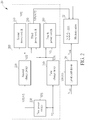
- FIG. 2 shows a memory system 20 according to one embodiment of the present invention.
- the memory system 20 includes a voltage control device 200 and a memory array 22 .
- the voltage control devices 100 and 200 have similar structures and can be operated with similar principles.
- the memory array 22 is coupled to the voltage control device 200 , and can include a plurality of memory cells 22 A.
- the voltage control device 200 can enter the first mode.
- the output terminal of the first power switch 230 will output the first application voltage VP 1 generated by the first charge pump 210 , so that the second charge pump 220 can generate the second application voltage VP 2 by raising the first application voltage VP 1 , and the second power switch 240 can output the second application voltage VP 2 through its output terminal.
- the second application voltage VP 2 can be higher than the first application voltage VP 1
- the first application voltage VP 1 can be higher than the first system voltage V 1 . Consequently, the memory array 22 can receive the second application voltage VP 2 as the erase voltage, and perform the erase operation to at least one memory cell 22 A accordingly.
- the voltage control device 200 can enter the second mode.
- the output terminal of the first power switch 230 can output the first system voltage V 1
- the first charge pump 210 and the second charge pump 220 can generate the first application voltage VP 1 and the second application voltage VP 2 , which are substantially the same, both are generated according to the first system voltage V 1 .
- the third power switch 250 can output the first application voltage VP 1 and the second application voltage VP 2 at the same time to cope with the large current load required by program operation.
- the memory array 22 can receive the first application voltage VP 1 and the second application VP 2 as the program voltage, and perform the program operation to at least one memory cell 22 A accordingly.
- the external input logic voltage V ctrl1 when performing the usual selection operations or read operations to the memory cells 22 A in the memory array 22 , the external input logic voltage V ctrl1 may be a lower operation voltage, for example, the input logic voltage V ctrl1 may be between 1.2V and 2V.
- the memory system 20 may further include a level shift driver 24 .
- the level shift driver 24 can be coupled to the voltage control device 200 and the memory array 22 , and can shift the level of the input logic voltage V ctrl1 to generate a driving control voltage V ctrl2 for controlling the memory array 22 .
- the level shift driver 24 can output the corresponding driving control voltage V ctrl2 according to the input logic voltage V ctrl1 , so that the high level of the driving control voltage V ctrl2 can be, for example, close to the first system voltage V 1 to drive the memory cells 22 A in the memory array 22 .
- the first system voltages V 1 generated by the constant voltage sources in different memory systems may also be different.
- the first system voltages V 1 can be between the minimum value 2.5V and maximum value 5.7V. If the high level of the input logic voltage V ctrl1 is between 1.2V and 1.98V, and the level shift driver 24 shifts the input logic voltage V ctrl1 to be close to the first system voltage V 1 , then the pull-up transistors and the pull-down transistors in the level shift driver 24 may be disproportionally biased.
- the pull-up transistors and the pull-down transistors of the level shift driver 24 will be disproportionally biased and will be turned on simultaneously, thereby lowering the efficiency of the level shift driver 24 .
- the level shift driver 24 may have to select the pull-up transistors and the pull-down transistors of proper sizes according to the actual operation conditions.
- the voltage control device 200 can further include a fourth power switch 260 .
- the fourth power switch 260 has a first input terminal, a second input terminal, and an output terminal.
- the first input terminal of the fourth power switch 260 can receive the first system voltage V 1
- the second input terminal of the fourth power switch 260 can be coupled to the output terminal of the first charge pump 210
- the output terminal of the fourth power switch 260 can be coupled to the level shift driver 24 .
- the voltage control device 200 can enter the third mode.
- the output terminal of the fourth power switch 260 can output the first application voltage VP 1 generated by the first charge pump 210 , so that the level shift driver 24 can shift the input logic voltage V ctrl1 according to the first application voltage VP 1 .
- the first application voltage VP 1 can be set to have a predetermined value that is greater than the minimum value of the first system voltage VP 1 (e.g. 2.5V) and smaller than the maximum value of the first system voltage VP 1 (e.g. 5.7V). That is, the predetermined value of the first application voltage VP 1 can be set between the minimum value and the maximum value of the first system voltage V 1 , for example but not limited to 3.5V, which is between 2.5V and 5.7V.
- the level shift driver 24 can receive the first application voltage VP 1 to shift the input logic voltage and generate the driving control voltage V ctrl2 , allowing the pull-up transistors and the pull-down transistors in the level shift driver 24 to be proportionally biased. Therefore, the voltage raising speed can be increased, and the area of the level shift driver 24 can be reduced. That is, with the first charge pump 210 and the fourth power switch 260 , the level shift driver 24 can receive the first application voltage VP 1 with a predetermined and fixed value. Therefore, the poor efficiency caused by the variation of the first system voltages V 1 in different memory system can be avoided, and the level shift driver 24 can be implemented with transistors of smaller sizes, reducing the area of the system.
- the first charge pump 210 may stop generating the first application voltage VP 1 .
- the fourth power switch 260 can output the first system voltage V 1 to the level shift driver 24 so as to prevent the memory system 22 from being floating.
- the first application voltage VP 1 generated by the first charge pump 210 would be a high voltage for the erase operation or the program operation.
- the first application voltage VP 1 may be greater than the bias voltage required by the level shift driver 24 . Therefore, the fourth power switch 260 can output the first system voltage V 1 to the level shift driver 24 in this case.
- the voltage control device and the memory system provided by the embodiments of the present invention can use the internal charge pump more efficiently to generate the required voltages, thereby reducing the area of the charge pumps.
- the voltage control device when applied to the memory system, can further generate proper operation voltages for the level shift driver, so the level shift driver can shift the level of the logic control signals more efficiently, and the overall area of the memory system can be reduced.
Landscapes
- Engineering & Computer Science (AREA)
- Physics & Mathematics (AREA)
- General Physics & Mathematics (AREA)
- Computer Security & Cryptography (AREA)
- Theoretical Computer Science (AREA)
- Power Engineering (AREA)
- Microelectronics & Electronic Packaging (AREA)
- Chemical & Material Sciences (AREA)
- Computer Hardware Design (AREA)
- Signal Processing (AREA)
- Computer Networks & Wireless Communication (AREA)
- Automation & Control Theory (AREA)
- Pure & Applied Mathematics (AREA)
- General Engineering & Computer Science (AREA)
- Mathematical Optimization (AREA)
- Radar, Positioning & Navigation (AREA)
- Electromagnetism (AREA)
- Mathematical Analysis (AREA)
- Computational Mathematics (AREA)
- Materials Engineering (AREA)
- Crystallography & Structural Chemistry (AREA)
- Semiconductor Memories (AREA)
- Read Only Memory (AREA)
Priority Applications (1)
| Application Number | Priority Date | Filing Date | Title |
|---|---|---|---|
| US16/365,661 US10693369B2 (en) | 2018-05-29 | 2019-03-26 | Voltage control device applied in a memory system |
Applications Claiming Priority (5)
| Application Number | Priority Date | Filing Date | Title |
|---|---|---|---|
| US201862677196P | 2018-05-29 | 2018-05-29 | |
| TW107142468 | 2018-11-28 | ||
| TW107142468A TWI669714B (zh) | 2018-05-29 | 2018-11-28 | 電壓控制裝置及記憶體系統 |
| TW107142468A | 2018-11-28 | ||
| US16/365,661 US10693369B2 (en) | 2018-05-29 | 2019-03-26 | Voltage control device applied in a memory system |
Publications (2)
| Publication Number | Publication Date |
|---|---|
| US20190372456A1 US20190372456A1 (en) | 2019-12-05 |
| US10693369B2 true US10693369B2 (en) | 2020-06-23 |
Family
ID=66647244
Family Applications (2)
| Application Number | Title | Priority Date | Filing Date |
|---|---|---|---|
| US16/365,661 Active US10693369B2 (en) | 2018-05-29 | 2019-03-26 | Voltage control device applied in a memory system |
| US16/421,820 Active 2040-12-16 US11404958B2 (en) | 2018-05-29 | 2019-05-24 | Random code generator and associated random code generating method |
Family Applications After (1)
| Application Number | Title | Priority Date | Filing Date |
|---|---|---|---|
| US16/421,820 Active 2040-12-16 US11404958B2 (en) | 2018-05-29 | 2019-05-24 | Random code generator and associated random code generating method |
Country Status (5)
| Country | Link |
|---|---|
| US (2) | US10693369B2 (de) |
| EP (1) | EP3576341B1 (de) |
| JP (1) | JP6905271B2 (de) |
| CN (2) | CN110544495B (de) |
| TW (2) | TWI669714B (de) |
Cited By (7)
| Publication number | Priority date | Publication date | Assignee | Title |
|---|---|---|---|---|
| US11756633B2 (en) | 2021-01-26 | 2023-09-12 | Kioxia Corporation | Semiconductor storage device |
| US11817159B2 (en) | 2020-07-16 | 2023-11-14 | Changxin Memory Technologies, Inc. | Circuit for detecting anti-fuse memory cell state and memory |
| US11817163B2 (en) | 2020-07-16 | 2023-11-14 | Changxin Memory Technologies, Inc. | Circuit for detecting state of anti-fuse storage unit and memory device thereof |
| US11854605B2 (en) | 2020-07-16 | 2023-12-26 | Changxin Memory Technologies, Inc. | State detection circuit for anti-fuse memory cell, and memory |
| US11854633B2 (en) | 2020-07-16 | 2023-12-26 | Changxin Memory Technologies, Inc. | Anti-fuse memory cell state detection circuit and memory |
| US12531123B2 (en) | 2023-07-13 | 2026-01-20 | Ememory Technology Inc. | Non-volatile memory with auxiliary select gate line driver |
| US12592266B2 (en) | 2023-09-07 | 2026-03-31 | Samsung Electronics Co., Ltd. | Memory device including voltage generating circuit and operation method of memory device |
Families Citing this family (10)
| Publication number | Priority date | Publication date | Assignee | Title |
|---|---|---|---|---|
| TWI669714B (zh) * | 2018-05-29 | 2019-08-21 | 力旺電子股份有限公司 | 電壓控制裝置及記憶體系統 |
| US11056155B1 (en) * | 2018-06-20 | 2021-07-06 | Adesto Technologies Corporation | Nonvolatile memory devices, systems and methods with switching charge pump architectures |
| US11416416B2 (en) * | 2019-01-13 | 2022-08-16 | Ememory Technology Inc. | Random code generator with non-volatile memory |
| US11562784B2 (en) * | 2020-08-14 | 2023-01-24 | Micron Technology, Inc. | Apparatuses, systems, and methods for voltage based random number generation |
| US11557338B2 (en) | 2020-10-13 | 2023-01-17 | Ememory Technology Inc. | Non-volatile memory with multi-level cell array and associated program control method |
| TWI761140B (zh) * | 2021-03-18 | 2022-04-11 | 旺宏電子股份有限公司 | 記憶體晶片 |
| US20230047939A1 (en) * | 2021-08-13 | 2023-02-16 | Ememory Technology Inc. | Fuse-type one time programming memory cell |
| TWI792764B (zh) * | 2021-12-13 | 2023-02-11 | 華邦電子股份有限公司 | 記憶體陣列及其操作方法 |
| US11776636B2 (en) | 2022-01-09 | 2023-10-03 | Winbond Electronics Corp. | Memory array and operation method thereof |
| KR102942358B1 (ko) * | 2024-11-22 | 2026-03-19 | 연세대학교 산학협력단 | 자기 저항성 메모리 기반 puf 장치를 위한 라이트백 회로 및 이를 포함하는 puf 장치 |
Citations (17)
| Publication number | Priority date | Publication date | Assignee | Title |
|---|---|---|---|---|
| US5602794A (en) * | 1995-09-29 | 1997-02-11 | Intel Corporation | Variable stage charge pump |
| US5909141A (en) * | 1997-03-03 | 1999-06-01 | Mitsubishi Denki Kabushiki Kaisha | Step-up potential supply circuit and semiconductor storage device |
| EP1229548A1 (de) | 2001-02-06 | 2002-08-07 | STMicroelectronics S.r.l. | Ladungspumpe für einen nichtflüchtige Speicher mit Lesespannungsregelung in der Gegenwart von Schräglauf von Adressen, und nichtflüchtiger Speicher mit solcher Ladungspumpe |
| US20030095423A1 (en) | 2001-11-21 | 2003-05-22 | Hirst B. Mark | Synchronous bridge rectifier |
| US6642773B2 (en) * | 2002-02-22 | 2003-11-04 | Ememory Technology Inc. | Charge pump circuit without body effects |
| US20080136500A1 (en) | 2006-12-11 | 2008-06-12 | Atmel Corporation | Charge pump for generation of multiple output-voltage levels |
| US7427889B2 (en) * | 2006-04-28 | 2008-09-23 | Ememory Technology Inc. | Voltage regulator outputting positive and negative voltages with the same offsets |
| US20120319762A1 (en) | 2011-06-17 | 2012-12-20 | Texas Instruments Incorporated | Power switch |
| TW201301730A (zh) | 2011-06-27 | 2013-01-01 | Winbond Electronics Corp | 升壓電路 |
| US20130063118A1 (en) * | 2011-09-09 | 2013-03-14 | Qui Vi Nguyen | Charge Pump System Dynamically Reconfigurable For Read And Program |
| US20130265103A1 (en) * | 2007-03-27 | 2013-10-10 | Elpida Memory, Inc. | Supply voltage generating circuit |
| US20130301175A1 (en) | 2009-06-30 | 2013-11-14 | Decicon, Inc. | Power switch with reverse current blocking capability |
| CN103457346A (zh) | 2012-06-01 | 2013-12-18 | 研祥智能科技股份有限公司 | 一种电源系统及其电源冗余控制电路 |
| TW201438388A (zh) | 2013-03-21 | 2014-10-01 | Univ Nat Taipei Technology | 可產生三倍輸入電壓的閘極驅動器及驅動方法 |
| TW201519693A (zh) | 2013-11-08 | 2015-05-16 | Coretronic Suzhou Co Ltd | 光源驅動器及其驅動方法 |
| US10236770B1 (en) * | 2017-11-27 | 2019-03-19 | National Chiao Tung University | High-voltage generator with multi-stage selection in low-voltage transistor process |
| US20190372456A1 (en) * | 2018-05-29 | 2019-12-05 | Ememory Technology Inc. | Voltage control device applied in a memory system |
Family Cites Families (13)
| Publication number | Priority date | Publication date | Assignee | Title |
|---|---|---|---|---|
| US5303190A (en) * | 1992-10-27 | 1994-04-12 | Motorola, Inc. | Static random access memory resistant to soft error |
| US6597603B2 (en) * | 2001-11-06 | 2003-07-22 | Atmel Corporation | Dual mode high voltage power supply for providing increased speed in programming during testing of low voltage non-volatile memories |
| JP2005235315A (ja) * | 2004-02-19 | 2005-09-02 | Elpida Memory Inc | 昇圧回路 |
| US8885819B2 (en) * | 2012-12-27 | 2014-11-11 | Intel Corporation | Fuse attestation to secure the provisioning of secret keys during integrated circuit manufacturing |
| US9436845B2 (en) * | 2014-03-25 | 2016-09-06 | Globalfoundries Inc. | Physically unclonable fuse using a NOR type memory array |
| TWI578325B (zh) * | 2015-08-18 | 2017-04-11 | 力旺電子股份有限公司 | 反熔絲型一次編程的記憶胞及其相關的陣列結構 |
| CA2952941C (en) * | 2016-01-08 | 2018-12-11 | Sidense Corp. | Puf value generation using an anti-fuse memory array |
| US9613714B1 (en) | 2016-01-19 | 2017-04-04 | Ememory Technology Inc. | One time programming memory cell and memory array for physically unclonable function technology and associated random code generating method |
| JP6495853B2 (ja) * | 2016-03-16 | 2019-04-03 | 株式会社東芝 | データ生成装置、電子デバイスおよび認証システム |
| US9851914B2 (en) * | 2016-03-24 | 2017-12-26 | Texas Instruments Incorporated | Random number generation in ferroelectric random access memory (FRAM) |
| US10020268B2 (en) * | 2016-04-13 | 2018-07-10 | Ememory Technology Inc. | Random number generator device and control method thereof |
| US9990181B2 (en) * | 2016-08-03 | 2018-06-05 | Micron Technology, Inc. | Apparatuses and methods for random number generation |
| JP6503395B2 (ja) * | 2016-10-12 | 2019-04-17 | イーメモリー テクノロジー インコーポレイテッド | 静電放電回路 |
-
2018
- 2018-11-28 TW TW107142468A patent/TWI669714B/zh active
- 2018-12-26 CN CN201811604128.3A patent/CN110544495B/zh active Active
-
2019
- 2019-03-26 US US16/365,661 patent/US10693369B2/en active Active
- 2019-05-24 CN CN201910439421.7A patent/CN110544500B/zh active Active
- 2019-05-24 TW TW108117981A patent/TWI715048B/zh active
- 2019-05-24 EP EP19176424.0A patent/EP3576341B1/de active Active
- 2019-05-24 US US16/421,820 patent/US11404958B2/en active Active
- 2019-05-24 JP JP2019097272A patent/JP6905271B2/ja active Active
Patent Citations (18)
| Publication number | Priority date | Publication date | Assignee | Title |
|---|---|---|---|---|
| US5602794A (en) * | 1995-09-29 | 1997-02-11 | Intel Corporation | Variable stage charge pump |
| US5909141A (en) * | 1997-03-03 | 1999-06-01 | Mitsubishi Denki Kabushiki Kaisha | Step-up potential supply circuit and semiconductor storage device |
| EP1229548A1 (de) | 2001-02-06 | 2002-08-07 | STMicroelectronics S.r.l. | Ladungspumpe für einen nichtflüchtige Speicher mit Lesespannungsregelung in der Gegenwart von Schräglauf von Adressen, und nichtflüchtiger Speicher mit solcher Ladungspumpe |
| US20030095423A1 (en) | 2001-11-21 | 2003-05-22 | Hirst B. Mark | Synchronous bridge rectifier |
| US6642773B2 (en) * | 2002-02-22 | 2003-11-04 | Ememory Technology Inc. | Charge pump circuit without body effects |
| US7427889B2 (en) * | 2006-04-28 | 2008-09-23 | Ememory Technology Inc. | Voltage regulator outputting positive and negative voltages with the same offsets |
| US20080136500A1 (en) | 2006-12-11 | 2008-06-12 | Atmel Corporation | Charge pump for generation of multiple output-voltage levels |
| US20130265103A1 (en) * | 2007-03-27 | 2013-10-10 | Elpida Memory, Inc. | Supply voltage generating circuit |
| US20130301175A1 (en) | 2009-06-30 | 2013-11-14 | Decicon, Inc. | Power switch with reverse current blocking capability |
| US20120319762A1 (en) | 2011-06-17 | 2012-12-20 | Texas Instruments Incorporated | Power switch |
| TW201301730A (zh) | 2011-06-27 | 2013-01-01 | Winbond Electronics Corp | 升壓電路 |
| US20130063118A1 (en) * | 2011-09-09 | 2013-03-14 | Qui Vi Nguyen | Charge Pump System Dynamically Reconfigurable For Read And Program |
| CN103457346A (zh) | 2012-06-01 | 2013-12-18 | 研祥智能科技股份有限公司 | 一种电源系统及其电源冗余控制电路 |
| TW201438388A (zh) | 2013-03-21 | 2014-10-01 | Univ Nat Taipei Technology | 可產生三倍輸入電壓的閘極驅動器及驅動方法 |
| TW201519693A (zh) | 2013-11-08 | 2015-05-16 | Coretronic Suzhou Co Ltd | 光源驅動器及其驅動方法 |
| CN104640267A (zh) | 2013-11-08 | 2015-05-20 | 苏州璨宇光学有限公司 | 光源驱动器及其驱动方法 |
| US10236770B1 (en) * | 2017-11-27 | 2019-03-19 | National Chiao Tung University | High-voltage generator with multi-stage selection in low-voltage transistor process |
| US20190372456A1 (en) * | 2018-05-29 | 2019-12-05 | Ememory Technology Inc. | Voltage control device applied in a memory system |
Cited By (7)
| Publication number | Priority date | Publication date | Assignee | Title |
|---|---|---|---|---|
| US11817159B2 (en) | 2020-07-16 | 2023-11-14 | Changxin Memory Technologies, Inc. | Circuit for detecting anti-fuse memory cell state and memory |
| US11817163B2 (en) | 2020-07-16 | 2023-11-14 | Changxin Memory Technologies, Inc. | Circuit for detecting state of anti-fuse storage unit and memory device thereof |
| US11854605B2 (en) | 2020-07-16 | 2023-12-26 | Changxin Memory Technologies, Inc. | State detection circuit for anti-fuse memory cell, and memory |
| US11854633B2 (en) | 2020-07-16 | 2023-12-26 | Changxin Memory Technologies, Inc. | Anti-fuse memory cell state detection circuit and memory |
| US11756633B2 (en) | 2021-01-26 | 2023-09-12 | Kioxia Corporation | Semiconductor storage device |
| US12531123B2 (en) | 2023-07-13 | 2026-01-20 | Ememory Technology Inc. | Non-volatile memory with auxiliary select gate line driver |
| US12592266B2 (en) | 2023-09-07 | 2026-03-31 | Samsung Electronics Co., Ltd. | Memory device including voltage generating circuit and operation method of memory device |
Also Published As
| Publication number | Publication date |
|---|---|
| CN110544500B (zh) | 2021-06-29 |
| TWI669714B (zh) | 2019-08-21 |
| TW202004757A (zh) | 2020-01-16 |
| CN110544495B (zh) | 2021-06-01 |
| TWI715048B (zh) | 2021-01-01 |
| CN110544500A (zh) | 2019-12-06 |
| US20190369966A1 (en) | 2019-12-05 |
| CN110544495A (zh) | 2019-12-06 |
| TW202004746A (zh) | 2020-01-16 |
| JP2019207692A (ja) | 2019-12-05 |
| JP6905271B2 (ja) | 2021-07-21 |
| EP3576341A1 (de) | 2019-12-04 |
| EP3576341B1 (de) | 2021-04-14 |
| US11404958B2 (en) | 2022-08-02 |
| US20190372456A1 (en) | 2019-12-05 |
Similar Documents
| Publication | Publication Date | Title |
|---|---|---|
| US10693369B2 (en) | Voltage control device applied in a memory system | |
| US10096368B2 (en) | Power switch circuit for non-volatile memory | |
| US7826297B2 (en) | Power supply switching circuit | |
| US7551507B2 (en) | Power supply circuit and semiconductor memory | |
| US9985519B2 (en) | Voltage generation circuit | |
| EP3595153B1 (de) | Spannungssteuerungsvorrichtung | |
| US10790821B1 (en) | Power switch circuit capable of reducing leakage currents | |
| US20100124140A1 (en) | Power supply circuit and nand-type flash memory | |
| CN107453599B (zh) | 多电压输出的正压电荷泵 | |
| US7576523B2 (en) | Power supply circuit and semiconductor memory | |
| US6385099B1 (en) | Reducing level shifter standby power consumption | |
| US20140307499A1 (en) | Booster circuit | |
| US7030684B2 (en) | High voltage switch circuit of semiconductor device | |
| US10268250B2 (en) | Semiconductor device having active mode and standby mode | |
| CN103730150B (zh) | 一种电平移位电路 | |
| CN105427779B (zh) | 用于升压的装置和方法以及包含该装置的显示面板驱动器 | |
| US7576592B2 (en) | Charge pump circuit and method of controlling the same | |
| US9837426B2 (en) | Voltage switching circuit and semiconductor apparatus including the same | |
| CN107437434B (zh) | 高压电平位移电路和非易失性存储器 | |
| US12014783B2 (en) | Driving circuit for non-volatile memory | |
| US20250300658A1 (en) | Voltage level shifter | |
| WO1998027477A1 (en) | A regulator system for charge pump circuits | |
| US9874892B2 (en) | Internal voltage generation device | |
| KR100224663B1 (ko) | 고전압 선택회로 |
Legal Events
| Date | Code | Title | Description |
|---|---|---|---|
| AS | Assignment |
Owner name: EMEMORY TECHNOLOGY INC., TAIWAN Free format text: ASSIGNMENT OF ASSIGNORS INTEREST;ASSIGNORS:KU, WEI-MING;ONG, WEI-CHIANG;REEL/FRAME:048707/0222 Effective date: 20190322 |
|
| FEPP | Fee payment procedure |
Free format text: ENTITY STATUS SET TO UNDISCOUNTED (ORIGINAL EVENT CODE: BIG.); ENTITY STATUS OF PATENT OWNER: SMALL ENTITY |
|
| FEPP | Fee payment procedure |
Free format text: ENTITY STATUS SET TO SMALL (ORIGINAL EVENT CODE: SMAL); ENTITY STATUS OF PATENT OWNER: SMALL ENTITY |
|
| STPP | Information on status: patent application and granting procedure in general |
Free format text: DOCKETED NEW CASE - READY FOR EXAMINATION |
|
| STPP | Information on status: patent application and granting procedure in general |
Free format text: NOTICE OF ALLOWANCE MAILED -- APPLICATION RECEIVED IN OFFICE OF PUBLICATIONS |
|
| STPP | Information on status: patent application and granting procedure in general |
Free format text: PUBLICATIONS -- ISSUE FEE PAYMENT RECEIVED |
|
| STCF | Information on status: patent grant |
Free format text: PATENTED CASE |
|
| MAFP | Maintenance fee payment |
Free format text: PAYMENT OF MAINTENANCE FEE, 4TH YR, SMALL ENTITY (ORIGINAL EVENT CODE: M2551); ENTITY STATUS OF PATENT OWNER: SMALL ENTITY Year of fee payment: 4 |