US10609243B2 - Image capturing apparatus, image capturing system, and movable apparatus - Google Patents
Image capturing apparatus, image capturing system, and movable apparatus Download PDFInfo
- Publication number
- US10609243B2 US10609243B2 US15/711,105 US201715711105A US10609243B2 US 10609243 B2 US10609243 B2 US 10609243B2 US 201715711105 A US201715711105 A US 201715711105A US 10609243 B2 US10609243 B2 US 10609243B2
- Authority
- US
- United States
- Prior art keywords
- temperature
- reference signal
- signal
- circuit
- signal output
- Prior art date
- Legal status (The legal status is an assumption and is not a legal conclusion. Google has not performed a legal analysis and makes no representation as to the accuracy of the status listed.)
- Active, expires
Links
Images


Classifications
-
- H—ELECTRICITY
- H04—ELECTRIC COMMUNICATION TECHNIQUE
- H04N—PICTORIAL COMMUNICATION, e.g. TELEVISION
- H04N23/00—Cameras or camera modules comprising electronic image sensors; Control thereof
- H04N23/50—Constructional details
- H04N23/54—Mounting of pick-up tubes, electronic image sensors, deviation or focusing coils
-
- H—ELECTRICITY
- H04—ELECTRIC COMMUNICATION TECHNIQUE
- H04N—PICTORIAL COMMUNICATION, e.g. TELEVISION
- H04N1/00—Scanning, transmission or reproduction of documents or the like, e.g. facsimile transmission; Details thereof
- H04N1/00976—Arrangements for regulating environment, e.g. removing static electricity
- H04N1/00978—Temperature control
-
- G—PHYSICS
- G01—MEASURING; TESTING
- G01K—MEASURING TEMPERATURE; MEASURING QUANTITY OF HEAT; THERMALLY-SENSITIVE ELEMENTS NOT OTHERWISE PROVIDED FOR
- G01K13/00—Thermometers specially adapted for specific purposes
-
- G—PHYSICS
- G01—MEASURING; TESTING
- G01K—MEASURING TEMPERATURE; MEASURING QUANTITY OF HEAT; THERMALLY-SENSITIVE ELEMENTS NOT OTHERWISE PROVIDED FOR
- G01K7/00—Measuring temperature based on the use of electric or magnetic elements directly sensitive to heat ; Power supply therefor, e.g. using thermoelectric elements
- G01K7/01—Measuring temperature based on the use of electric or magnetic elements directly sensitive to heat ; Power supply therefor, e.g. using thermoelectric elements using semiconducting elements having PN junctions
-
- H—ELECTRICITY
- H04—ELECTRIC COMMUNICATION TECHNIQUE
- H04N—PICTORIAL COMMUNICATION, e.g. TELEVISION
- H04N23/00—Cameras or camera modules comprising electronic image sensors; Control thereof
- H04N23/50—Constructional details
-
- H—ELECTRICITY
- H04—ELECTRIC COMMUNICATION TECHNIQUE
- H04N—PICTORIAL COMMUNICATION, e.g. TELEVISION
- H04N25/00—Circuitry of solid-state image sensors [SSIS]; Control thereof
- H04N25/60—Noise processing, e.g. detecting, correcting, reducing or removing noise
-
- H—ELECTRICITY
- H04—ELECTRIC COMMUNICATION TECHNIQUE
- H04N—PICTORIAL COMMUNICATION, e.g. TELEVISION
- H04N25/00—Circuitry of solid-state image sensors [SSIS]; Control thereof
- H04N25/60—Noise processing, e.g. detecting, correcting, reducing or removing noise
- H04N25/61—Noise processing, e.g. detecting, correcting, reducing or removing noise the noise originating only from the lens unit, e.g. flare, shading, vignetting or "cos4"
-
- H—ELECTRICITY
- H04—ELECTRIC COMMUNICATION TECHNIQUE
- H04N—PICTORIAL COMMUNICATION, e.g. TELEVISION
- H04N25/00—Circuitry of solid-state image sensors [SSIS]; Control thereof
- H04N25/60—Noise processing, e.g. detecting, correcting, reducing or removing noise
- H04N25/616—Noise processing, e.g. detecting, correcting, reducing or removing noise involving a correlated sampling function, e.g. correlated double sampling [CDS] or triple sampling
-
- H—ELECTRICITY
- H04—ELECTRIC COMMUNICATION TECHNIQUE
- H04N—PICTORIAL COMMUNICATION, e.g. TELEVISION
- H04N25/00—Circuitry of solid-state image sensors [SSIS]; Control thereof
- H04N25/60—Noise processing, e.g. detecting, correcting, reducing or removing noise
- H04N25/67—Noise processing, e.g. detecting, correcting, reducing or removing noise applied to fixed-pattern noise, e.g. non-uniformity of response
-
- H—ELECTRICITY
- H04—ELECTRIC COMMUNICATION TECHNIQUE
- H04N—PICTORIAL COMMUNICATION, e.g. TELEVISION
- H04N25/00—Circuitry of solid-state image sensors [SSIS]; Control thereof
- H04N25/70—SSIS architectures; Circuits associated therewith
- H04N25/71—Charge-coupled device [CCD] sensors; Charge-transfer registers specially adapted for CCD sensors
- H04N25/745—Circuitry for generating timing or clock signals
-
- H—ELECTRICITY
- H04—ELECTRIC COMMUNICATION TECHNIQUE
- H04N—PICTORIAL COMMUNICATION, e.g. TELEVISION
- H04N25/00—Circuitry of solid-state image sensors [SSIS]; Control thereof
- H04N25/70—SSIS architectures; Circuits associated therewith
- H04N25/76—Addressed sensors, e.g. MOS or CMOS sensors
-
- H04N5/357—
-
- H04N5/3572—
-
- H04N5/3575—
-
- H04N5/365—
-
- H04N5/374—
-
- H04N5/3765—
Definitions
- the present invention relates to an image capturing apparatus, an image capturing system, and a movable apparatus.
- Japanese Patent Laid-Open No. 2012-151664 describes mounting a pixel array portion and a diode serving as a temperature sensor and obtaining a temperature measurement value based on the difference of a diode voltage generated when a diode current is changed, thereby improving the accuracy of temperature measurement.
- the present invention provides a technique advantageous in more accurately detecting a temperature.
- One of aspects of the present invention provides an image capturing apparatus comprising: a plurality of pixels arranged on a substrate; a temperature signal output unit arranged on the substrate and configured to output a temperature signal representing a temperature; and a reference signal output unit arranged on the substrate and configured to output a reference signal used to correct the temperature signal, wherein the temperature signal output unit and the reference signal output unit are arranged in regions different from each other on the substrate.
- FIG. 1 is a block diagram showing the arrangement of an image capturing apparatus and an image capturing system according to the first embodiment
- FIG. 2 is a circuit diagram showing an example of the arrangement of a pixel
- FIG. 3 is a block diagram showing an example of implementation of a part of the image capturing apparatus
- FIG. 4 is a timing chart showing the timing of signal read
- FIG. 5 is a sectional view showing an example of the arrangement of a temperature detection element
- FIG. 6 is a flowchart showing an example of the operation of the image capturing system
- FIG. 7 is a block diagram showing the arrangement of an image capturing apparatus according to the second embodiment.
- FIG. 8 is a view showing an example of the arrangement of a movable apparatus.
- FIG. 9 is a block diagram showing the system arrangement of the movable apparatus.
- FIG. 1 shows the arrangement of an image capturing apparatus 10 and an image capturing system 30 according to the first embodiment of the present invention.
- the image capturing system 30 can include the image capturing apparatus 10 and a calculator 20 .
- the image capturing apparatus 10 can be configured to capture an image and also output a temperature signal representing a temperature and a reference signal used to correct the temperature signal.
- the calculator 20 can be configured to obtain a corrected temperature by correcting the temperature signal based on the reference signal.
- the image capturing apparatus 10 can output the temperature signal and the reference signal using either an analog signal format or a digital signal format.
- An example in which the image capturing apparatus 10 outputs the temperature signal and the reference signal using a digital signal format will be described below.
- the first embodiment uses the terms “image capturing apparatus” and “image capturing system” while distinguishing one from the other. However, these expressions are used merely for the sake of convenience with focus on the presence/absence of the calculator.
- the image capturing system 30 in the first embodiment may be called an image capturing apparatus.
- the image capturing apparatus 10 can include a pixel array 101 , a vertical selection circuit 102 , a plurality of column circuits 103 , sensor circuits 123 a and 123 b , horizontal selection circuits 104 , a signal processing circuit 105 , a temperature sensor 106 , a reference signal generating circuit 312 , and a counter 314 .
- the image capturing apparatus 10 can also include a timing generator 109 .
- the timing generator 109 generates various kinds of signals to control timings, as will be described later.
- the pixel array 101 , the vertical selection circuit 102 , the column circuits 103 , the sensor circuits 123 a and 123 b , the horizontal selection circuits 104 , the signal processing circuit 105 , the temperature sensor 106 , the reference signal generating circuit 312 , the counter 314 , and the timing generator 109 can be arranged on one substrate SUB.
- the one substrate SUB is, for example, a semiconductor chip separated from a semiconductor wafer by dicing.
- the pixel array 101 includes a plurality of pixels 100 that are arranged to form a plurality of rows and a plurality of columns.
- the pixels 100 arranged on the same row are controlled by a control signal supplied from the vertical selection circuit 102 via a common control line CL.
- the pixels 100 arranged on the same column are connected to a common signal line VL.
- the signal line VL can be connected to a current source.
- Each pixel 100 outputs, for example, a noise signal N or an optical signal S to the signal line VL.
- Each signal line VL can be connected to one column circuit 103 .
- the signal lines VL connected to the pixels 100 that form odd-numbered columns are connected to the column circuits 103 arranged on one side of the pixel array 101 .
- the signal lines VL connected to the pixels 100 that form even-numbered columns are connected to the column circuits 103 arranged on the other side of the pixel array 101 .
- Each column circuit 103 converts the analog signals of the noise signal and the optical signal output from the pixel 100 into a noise signal and an optical signal in a digital format.
- Each of the plurality of column circuits 103 outputs a set of a noise signal and an optical signal.
- Each horizontal selection circuit 104 sequentially selects one set from a plurality of sets and supplies the noise signal and the optical signal of the selected set to the signal processing circuit 105 .
- the temperature sensor 106 can be configured to output a temperature signal and a reference signal when a current of a first current value is supplied to a temperature detection element to be described later and also output a temperature signal and a reference signal when a current of a second current value is supplied to the temperature detection element.
- the sensor circuit 123 a converts a temperature signal into a temperature signal in a digital format.
- the sensor circuit 123 b converts a reference signal into a reference signal in a digital format.
- the sensor circuits 123 a and 123 b can have the same arrangement as the column circuit 103 .
- the signal processing circuit 105 can be configured to generate a pixel signal by calculating the difference between the noise signal and the optical signal in the digital format.
- the signal processing circuit 105 can also be configured to obtain a corrected temperature by correcting the temperature signal in the digital format based on the reference signal in the digital format.
- the temperature sensor 106 is connected to one horizontal selection circuit 104 via the sensor circuits 123 a and 123 b and also connected to the other horizontal selection circuit 104 via the other sensor circuits 123 a and 123 b .
- the pixel array 101 includes the pixels 100 that are not connected to the column circuits 103 .
- the pixels 100 that are not connected to the column circuits 103 may be connected to the current source (not shown).
- FIG. 2 shows an example of the arrangement of the pixel 100 .
- Control signals P_RES, P_TX 1 , P_TX 2 , and P_SEL are control signals supplied to the pixel 100 via the control line CL described above.
- One pixel 100 shown in FIG. 2 includes two photoelectric converters 201 - 1 and 201 - 2 .
- the one pixel 100 can include one microlens shared by the two photoelectric converters 201 - 1 and 201 - 2 .
- the two photoelectric converters 201 - 1 and 201 - 2 can be, for example, photodiodes.
- the pixel 100 can include a charge-voltage converter 203 (floating diffusion) and transfer MOS transistors 202 - 1 and 202 - 2 .
- the transfer MOS transistor 202 - 1 transfers charge in the photoelectric converter 201 - 1 to the charge-voltage converter 203 when the transfer control signal P_TX 1 is activated.
- the transfer MOS transistor 202 - 2 transfers charge in the photoelectric converter 201 - 2 to the charge-voltage converter 203 when the transfer control signal P_TX 2 is activated.
- the charge-voltage converter 203 is formed by a capacitor and converts charge (charge amount) into a voltage.
- the pixel 100 can also include a reset MOS transistor 204 , an amplification MOS transistor 205 , and a select MOS transistor 206 .
- the reset MOS transistor 204 resets the charge-voltage converter 203 to a reset voltage when the reset control signal P_RES is activated.
- the amplification MOS transistor 205 forms a source follower circuit together with the current source (not shown) connected to the signal line VL, and outputs a signal corresponding to the voltage of the charge-voltage converter 203 to the signal line VL. In other words, a signal corresponding to the charge (charge amount) transferred to the charge-voltage converter 203 is output to the signal line VL.
- the select MOS transistor 206 connects the amplification MOS transistor 205 to the signal line VL when the select control signal P_SEL is activated. That the select control signal P_SEL is selected means that the pixels 100 of the row to which the select control signal P_SEL is supplied are selected.
- one pixel 100 may be formed by one photoelectric converter, one charge-voltage converter, one reset MOS transistor, one transfer MOS transistor, one amplification MOS transistor, and one select MOS transistor.
- the select MOS transistor 206 is not necessary.
- the image capturing apparatus 10 is constructed in a form of a MOS image sensor.
- the image capturing apparatus 10 may be constructed in another form such as a CCD image sensor.
- FIG. 3 shows an example of implementation of a part of the image capturing apparatus 10 shown in FIG. 1 .
- the temperature sensor 106 includes a temperature signal generator 411 and a reference signal generator 412 .
- the temperature signal generator 411 and the reference signal generator 412 can be arranged in regions different from each other on the substrate SUB.
- the temperature signal generator 411 generates a temperature signal representing a temperature.
- the reference signal generator 412 generates a reference signal used to correct the temperature signal.
- the temperature signal generated by the temperature signal generator 411 is supplied to the sensor circuit 123 a .
- the reference signal generated by the reference signal generator 412 is supplied to the sensor circuit 123 b .
- the temperature signal generator 411 and the sensor circuit 123 a form a temperature signal output unit 421 that outputs the temperature signal.
- the reference signal generator 412 and the sensor circuit 123 b form a reference signal output unit 422 that outputs the reference signal.
- the signal line VL connected to the pixel 100 is connected to the column
- the characteristic of a circuit in a path to generate a temperature signal and output it or a circuit that supplies a signal to the circuit in the path changes between the image capturing apparatuses 10 . This is because an error that occurs at the time of manufacturing can change for each semiconductor wafer, or even on the same wafer, and an error that occurs at the time of manufacturing can change if the locations of elements to be manufactured are far apart.
- the circuit is, for example, the temperature signal output unit 421 , the sensor circuit 123 a , the reference signal generating circuit 312 , or the counter 314 .
- the reference signal output unit 422 that outputs the reference signal used to correct the temperature signal output from the temperature signal output unit 421 is arranged on the same substrate SUB as the temperature signal output unit 421 .
- the temperature dependency of the reference signal output from the reference signal output unit 422 is lower than the temperature dependency of the temperature signal output from the temperature signal output unit 421 .
- the temperature signal output unit 421 and the reference signal output unit 422 which are arranged on the same substrate SUB can have the same manufacturing error (for example, the line width error of the pattern).
- the reference signal output unit 422 includes an element having mutuality with an element that causes the error of the temperature signal output from the temperature signal output unit 421 . For this reason, the temperature signal output from the temperature signal output unit 421 can be corrected based on the reference signal output from the reference signal output unit 422 . A temperature (corrected temperature) whose error is reduced or removed can thus be obtained.
- a first temperature signal (analog temperature signal) output from the temperature signal generator 411 is supplied to the sensor circuit 123 a .
- the sensor circuit 123 a A/D-converts the first temperature signal supplied from the temperature signal generator 411 and outputs a digital signal corresponding to the first temperature signal as a temperature signal (digital temperature signal).
- the temperature signal output from the temperature signal generator 411 is expressed as the first temperature signal. This is a convenient expression in order to make a distinction between the signal and the temperature signal (digital temperature signal) output from the temperature signal output unit 421 (sensor circuit 123 a ).
- Both the signal output from the temperature signal generator 411 and the signal output from the temperature signal output unit 421 (sensor circuit 123 a ) are temperature signals.
- the sensor circuit 123 a can include a first amplifier 350 a that amplifies the first temperature signal output from the temperature signal generator 411 .
- the first amplifier 350 a may be absent.
- the sensor circuit 123 a can include a first A/D converter 360 a that converts the first temperature signal output from the temperature signal generator 411 via the first amplifier 350 a into a digital signal, thereby generating a digital temperature signal.
- the first amplifier 350 a is, for example, an amplifier having a variable gain. If the first amplifier 350 a is absent, the temperature signal output from the temperature signal generator 411 can be input to the first A/D converter 360 a.
- the first A/D converter 360 a compares the amplified first temperature signal (analog signal) supplied from the first amplifier 350 a with a reference signal Sref supplied from the reference signal generating circuit 312 .
- the first A/D converter 360 a decides, as a digital signal, a count value representing a time from the start of the comparison until inversion of the result of the comparison.
- a count value signal Scnt that provides the count value is supplied from the counter 314 .
- the counter 314 can be controlled by the timing generator 109 so as to start a count operation (time count operation) in accordance with the start of comparison.
- the first A/D converter 360 a includes, for example, a comparator 313 a and a storage unit 315 a .
- the comparator 313 a compares the amplified first temperature signal (analog signal) supplied from the first amplifier 350 a with the reference signal Sref supplied from the reference signal generating circuit 312 , and outputs a comparison result signal CR representing the comparison result.
- the comparison result signal CR can be, for example, a signal to be activated for a predetermined period when the comparison result is inverted.
- the storage unit 315 a receives and holds the count value of the count value signal Scnt when the comparison result signal CR is activated.
- the count value is the value of the digital temperature signal corresponding to the amplified first temperature signal (analog signal) supplied from the first amplifier 350 a.
- a first reference signal (analog reference signal) output from the reference signal generator 412 is supplied to the sensor circuit 123 b .
- the sensor circuit 123 b can have the same arrangement as the sensor circuit 123 a .
- the sensor circuit 123 b A/D-converts the first reference signal supplied from the reference signal generator 412 and outputs a digital signal corresponding to the first reference signal as a reference signal (digital reference signal).
- the reference signal output from the reference signal generator 412 is expressed as the first reference signal. This is a convenient expression in order to make a distinction between the signal and the reference signal (digital reference signal) output from the reference signal output unit 422 (sensor circuit 123 b ).
- Both the signal output from the reference signal generator 412 and the signal output from the reference signal output unit 422 (sensor circuit 123 b ) are reference signals.
- the sensor circuit 123 b can include a second amplifier 350 b that amplifies the first reference signal output from the reference signal generator 412 .
- the second amplifier 350 b may be absent.
- the sensor circuit 123 b can include a second A/D converter 360 b that converts the first reference signal output from the reference signal generator 412 via the second amplifier 350 b into a digital signal, thereby generating a digital reference signal.
- the second amplifier 350 b is, for example, an amplifier having a variable gain. If the second amplifier 350 b is absent, the reference signal output from the reference signal generator 412 can be input to the second A/D converter 360 b.
- the second A/D converter 360 b compares the amplified first reference signal (analog signal) supplied from the second amplifier 350 b with the reference signal Sref supplied from the reference signal generating circuit 312 .
- the second A/D converter 360 b decides, as a digital signal, a count value representing a time from the start of the comparison up to inversion of the result of the comparison.
- the count value signal Scnt that provides the count value is supplied from the counter 314 .
- the common reference signal Sref and count value signal Scnt can be supplied to the first A/D converter 360 a and the second A/D converter 360 b as signals (common signals) commonly used for A/D conversion.
- only one of the reference signal Sref and the count value signal Scnt may be supplied as a common signal to the first A/D converter 360 a and the second A/D converter 360 b , and the other may be generated individually for the first A/D converter 360 a and the second A/D converter 360 b . That is, at least one of the reference signal Sref and the count value signal Scnt can be supplied as a common signal to the first A/D converter 360 a and the second A/D converter 360 b .
- a reset signal P_CAMP_RST used to reset the first amplifier 350 a and the second amplifier 350 b can be supplied as a common signal from the timing generator 109 to the first amplifier 350 a and the second amplifier 350 b .
- the reference signal generating circuit 312 and the counter 314 form a signal generator 320 that generates the common signals.
- the column circuit 103 that processes a signal supplied from the pixel 100 via the signal line VL can have the same arrangement as the sensor circuits 123 a and 123 b .
- the column circuit 103 can include a column amplifier 350 that amplifies the signal output from the pixel 100 of a selected row to the signal line VL. However, the column amplifier 350 may be absent.
- the column amplifier 350 is, for example, an amplifier having a variable gain.
- the column circuit 103 can include an A/D converter 360 that converts the signal supplied from the pixel 100 via the column amplifier 350 into a digital signal. If the column amplifier 350 is absent, the signal output from the pixel 100 can be input to the A/D converter 360 .
- the horizontal selection circuit 104 can be configured to read signals from the storage unit 315 a of the sensor circuit 123 a , a storage unit 315 b of the sensor circuit 123 b , and storage units 315 of the plurality of column circuits 103 in a predetermined order and supply the signals to the signal processing circuit 105 .
- the horizontal selection circuit 104 can include a scanning circuit configured to decide which one of the storage unit 315 a of the sensor circuit 123 a , the storage unit 315 b of the sensor circuit 123 b , and the storage units 315 of the plurality of column circuits 103 should be selected.
- the horizontal selection circuit 104 can also include a multiplexer that can be formed by a plurality of switches controlled by the scanning circuit.
- the signal processing circuit 105 processes a signal supplied from the horizontal selection circuit 104 and outputs a signal obtained by the processing to an output pad 316 .
- the output pad 316 can be connected, by a bonding wire or the like, to a pin provided on a package that seals the substrate SUB.
- the reference signal generating circuit 312 includes, for example, a capacitor element and can generate the reference signal Sref by charging/discharging the capacitor element.
- the capacitance value of the capacitor element can vary between the image capturing apparatuses 10 due to the manufacturing process.
- the delay time of the count value signal Scnt can also vary between the image capturing apparatuses 10 . If the reference signal Sref and/or the count value signal Scnt varies between the image capturing apparatuses 10 , the temperature signal can vary between the image capturing apparatuses 10 even for the same temperature. In other words, the temperature signal can include an error caused by the manufacturing process.
- the image capturing apparatus 10 includes the reference signal output unit 422 that outputs the reference signal used to correct the temperature signal.
- the temperature dependency of the reference signal output from the reference signal output unit 422 is lower than the temperature dependency of the temperature signal output from the temperature signal output unit 421 . Hence, using the difference in the temperature dependency, a corrected temperature can be obtained by correcting the temperature signal using the reference signal.
- the sensor circuit 123 a configured to output the temperature signal and the sensor circuit 123 b configured to output the reference signal preferably have the same arrangement.
- the common signals (the reference signal Sref and the count value signal Scnt) are preferably supplied to the sensor circuits 123 a and 123 b . Accordingly, if error factors exist in the signal processes of the sensor circuits 123 a and 123 b , the error factors can be made equal to each other.
- G 1 be the conversion gain of the sensor circuit 123 a
- G 2 the conversion gain of the sensor circuit 123 b
- Each conversion gain includes an amplification gain G am of the amplifiers 350 a and 350 b and an A/D conversion gain G AD of the A/D converters 360 a and 360 b
- the corrected temperature can be obtained based on the ratio of the output value of the sensor circuit 123 a to the output value of the sensor circuit 123 b .
- G 1 and G 2 can be made almost equal by causing the sensor circuits 123 a and 123 b to have the same arrangement and using at least one or preferably both of the reference signal Sref and the count value signal Scnt as common signals. Accordingly, the error factor in the sensor circuit 123 a can be canceled or reduced by the error factor in the sensor circuit 123 b .
- K in equation (1) can be decided based on the relationship between the actual temperature and (output of output value of temperature signal generator 411 ⁇ G 1 )/(output of output value of reference signal generator 412 ⁇ G 2 ).
- the temperature signal output unit 421 and the reference signal output unit 422 are formed on the same substrate SUB. Hence, even if the characteristic of an element varies between the image capturing apparatuses 10 due to a manufacturing error, the difference in characteristic is small between elements having identical or similar arrangements in the temperature signal output unit 421 and the reference signal output unit 422 . Even if an element included in the temperature signal output unit 421 is an element that can cause a variation, correction of the temperature signal using the reference signal is enabled by forming the reference signal output unit 422 using an element with an arrangement identical or similar to the arrangement of the element.
- FIGS. 1 and 3 show an example in which the sensor circuits 123 a and 123 b are provided individually for the temperature signal generator 411 and the reference signal generator 412 .
- the sensor circuits 123 a and 123 b may be absent, or a sensor circuit common to the temperature signal generator 411 and the reference signal generator 412 may be provided. If the sensor circuit common to the temperature signal generator 411 and the reference signal generator 412 is provided, the outputs from the temperature signal generator 411 and the reference signal generator 412 can be A/D-converted by the common sensor circuit during periods different from each other.
- the temperature signal generator 411 can include, for example, resistors 301 a and 301 b , a first buffer circuit 302 a , a temperature detection element 303 , a current control switch 304 , a variable current source 305 , and a first amplification circuit 310 a .
- the resistors 301 a and 301 b form a voltage supply circuit that divides a power supply voltage VDD to generate a predetermined voltage and supplies it to the first buffer circuit 302 a . Since the predetermined voltage is decided by the ratio of the resistance values of the resistors 301 a and 301 b , the temperature dependency is reduced.
- the first buffer circuit 302 a outputs a signal according to the input voltage to the temperature detection element 303 .
- the first buffer circuit 302 a can have a high impedance.
- the first buffer circuit 302 a can include, for example, a voltage follower circuit or a source follower circuit.
- FIG. 3 shows an example in which the first buffer circuit 302 a is formed by a voltage follower circuit.
- the temperature detection element 303 can include, for example, a bipolar transistor such as an NPN bipolar transistor.
- the current-voltage characteristic of the bipolar transistor has temperature dependency, and the temperature can be detected using the current-voltage characteristic.
- the base voltage of the bipolar transistor is 2.6 V
- the emitter voltage is 3.3 V.
- the current control switch 304 is a switch configured to control whether to supply a current between the emitter and the collector of the bipolar transistor serving as the temperature detection element 303 .
- the current control switch 304 can be controlled by a current control signal P_BIAS_ON.
- the current control signal P_BIAS_ON can be generated by the timing generator 109 . If the temperature signal output unit 421 is not used (if the temperature is not detected), the current control switch 304 is turned off to prevent image quality degradation caused by light emission of the bipolar transistor and heat generation of the bipolar transistor and also to save power.
- the variable current source 305 is arranged between a ground line and the emitter of the bipolar transistor serving as the temperature detection element 303 .
- the variable current source 305 is a current source capable of changing the value of a current (emitter current) that flows to the temperature detection element 303 (bipolar transistor), and can be controlled by a bias control signal P_BIAS_ADD.
- the bias control signal P_BIAS_ADD can be controlled by the timing generator 109 .
- the difference in the emitter voltage when the emitter current is changed is acquired, and the temperature can be detected based on the difference.
- a temperature detection error derived from the nonlinear current-voltage characteristic of the bipolar transistor can be reduced.
- the variable current source 305 supplies a current of a first current value to the bipolar transistor serving as the temperature detection element 303 .
- the variable current source 305 supplies a current of a second current value different from the first current value to the bipolar transistor.
- the temperature can be detected based on the difference between the emitter voltage in the first period and the emitter voltage in the second period.
- the first current value is eight times larger than the second current value.
- the first amplification circuit 310 a can include, for example, a differential amplifier 306 , an input capacitor 307 a , a feedback capacitor 307 b , and a reset switch 308 .
- the input capacitor 307 a can be arranged between the input terminal of the first amplification circuit 310 a and the noninverting input terminal of the differential amplifier 306 .
- a reference voltage VREF can be applied to the inverting input terminal of the differential amplifier 306 .
- the feedback capacitor 307 b and the reset switch 308 can be arranged in parallel between the noninverting input terminal of the differential amplifier 306 and the output terminal of the differential amplifier 306 .
- the gain of the first amplification circuit 310 a is decided by the ratio of the input capacitor 307 a to the feedback capacitor 307 b .
- the gain of the first amplification circuit 310 a can be decided such that a voltage within the range of the level of the signal output from the pixel 100 to the signal line VL is output to the sensor circuit 123 a .
- the arrangement of the sensor circuit 123 a can thus be made equal to the arrangement of the column circuit 103 .
- the reset switch 308 can be controlled by a reset signal P_TEMP_COR.
- the reset signal P_TEMP_COR can be controlled by the timing generator 109 .
- the reset signal P_TEMP_COR is driven from an active state to an inactive state. Accordingly, the emitter voltage of the bipolar transistor when the current of the first current value is supplied to the bipolar transistor serving as the temperature detection element 303 is written to the feedback capacitor 307 b .
- the current of the second current value is supplied to the bipolar transistor, and the emitter voltage of the bipolar transistor changes.
- the first amplification circuit 310 a amplifies the difference between the emitter voltage of the bipolar transistor in the first period and the emitter voltage of the bipolar transistor in the second period and outputs the voltage. According to this method, the temperature detection error derived from the nonlinear current-voltage characteristic of the bipolar transistor can be reduced, as described above.
- the reference signal generator 412 can include resistors 301 c , 301 d , and 301 e , switches 309 and 311 , a second buffer circuit 302 b , and a second amplification circuit 310 b .
- the second buffer circuit 302 b can have the same arrangement as the first buffer circuit 302 a .
- the second amplification circuit 310 b can have the same arrangement as the first amplification circuit 310 a.
- the resistors 301 c , 301 d , and 301 e divide the power supply voltage VDD to generate a first voltage V 1 and a second voltage V 2 .
- a control signal P_VL is activated.
- a control signal P_VH is activated.
- the control signals P_VL and P_VH can be controlled by the timing generator 109 .
- the switch 311 is turned on in accordance with the activation of the control signal P_VL to apply the first voltage V 1 to the input terminal of the second buffer circuit 302 b .
- the switch 309 is turned on in accordance with the activation of the control signal P_VH to apply the second voltage V 2 to the input terminal of the second buffer circuit 302 b .
- the first voltage V 1 1.85 V
- the second voltage V 2 1.90 V.
- the second buffer circuit 302 b can include, for example, a voltage follower circuit or a source follower circuit.
- FIG. 3 shows an example in which the second buffer circuit 302 b is formed by a voltage follower circuit.
- the second amplification circuit 310 b can include, for example, the differential amplifier 306 , the input capacitor 307 a , the feedback capacitor 307 b , and the reset switch 308 .
- the input capacitor 307 a can be arranged between the input terminal of the second amplification circuit 310 b and the noninverting input terminal of the differential amplifier 306 .
- the reference voltage VREF can be applied to the inverting input terminal of the differential amplifier 306 .
- the feedback capacitor 307 b and the reset switch 308 can be arranged in parallel between the noninverting input terminal of the differential amplifier 306 and the output terminal of the differential amplifier 306 .
- the gain of the second amplification circuit 310 b is decided by the ratio of the input capacitor 307 a to the feedback capacitor 307 b .
- the gain of the second amplification circuit 310 b can be decided such that a voltage within the range of the level of the signal output from the pixel 100 to the signal line VL is output to the sensor circuit 123 b .
- the arrangement of the sensor circuit 123 b can thus be made equal to the arrangement of the column circuit 103 .
- the reset switch 308 can be controlled by the reset signal P_TEMP_COR.
- the reset signal P_TEMP_COR can be controlled by the timing generator 109 .
- the reset signal P_TEMP_COR is driven from an active state to an inactive state. Accordingly, the first voltage V 1 is applied to the second amplification circuit 310 b via the second buffer circuit 302 b , and the first voltage V 1 is written to the feedback capacitor 307 b .
- the second voltage V 2 is applied to the second amplification circuit 310 b via the second buffer circuit 302 b .
- the second amplification circuit 310 b amplifies the difference between the first voltage V 1 applied to the second amplification circuit 310 b in the first period and the second voltage V 2 applied to the second amplification circuit 310 b in the second period and outputs the voltage.
- the base voltage of the bipolar transistor serving as the temperature detection element 303 is 2.6 V, and the emitter voltage is 3.3 V.
- the first current value that is the current value of the current supplied by the variable current source 305 in the first period is 10 ⁇ A
- the second current value that is the current value of the current supplied by the variable current source 305 in the second period is 80 ⁇ A.
- the emitter voltage of the bipolar transistor when the first current value that is the current value of the current supplied by the variable current source 305 in the first period is 10 ⁇ A is about 1.85 V.
- the emitter voltage of the bipolar transistor when the second current value that is the current value of the current supplied by the variable current source 305 in the second period is 80 ⁇ A is about 1.90 V.
- the reference voltage VREF is 2.6 V.
- the gain of the first amplification circuit 310 a and the second amplification circuit 310 b is 10.
- the reference signal output unit 422 can include not the reference signal generator 412 but a pad to which a constant voltage is externally applied.
- a band gap reference circuit may be employed as the reference signal generator 412 .
- the temperature signal from the temperature signal generator 411 is input to the horizontal selection circuit 104 via the sensor circuit 123 a .
- the reference signal from the reference signal generator 412 is input to the horizontal selection circuit 104 via the sensor circuit 123 b .
- the temperature signal and the reference signal are output via the horizontal selection circuit 104 (selection circuit) that selects the signal of the pixel 100 .
- the calculator 20 arranged outside the image capturing apparatus 10 corrects the temperature signal based on the reference signal, thereby obtaining a corrected temperature.
- FIG. 4 shows the timings of the pixel signal read from the pixel 100 by the column circuit 103 , the temperature signal read from the temperature signal generator 411 by the sensor circuit 123 a , and the reference signal read from the reference signal generator 412 by the sensor circuit 123 b .
- the vertical selection circuit 102 activates the control signal P_SEL for the pixel 100 of the read target row to high level.
- the vertical selection circuit 102 inactivates the control signal P_RES for the pixel 100 of the read target row to low level, and cancels reset of the charge-voltage converter 203 of the pixel 100 of the read target row.
- the timing generator 109 activates the control signal P_TEMP_COR to high level, and the first amplification circuit 310 a of the temperature signal generator 411 and the second amplification circuit 310 b of the reference signal generator 412 are reset.
- the timing generator 109 activates the control signals P_BIAS_ON, P_BIAS_ADD, and P_VL to high level. Accordingly, the current of the first current value flows to the bipolar transistor serving as the temperature detection element 303 of the temperature signal generator 411 , and the first voltage V 1 is applied to the second buffer circuit 302 b of the reference signal generator 412 .
- the timing generator 109 inactivates the control signals P_CAMP_RST and P_TEMP_COR to low level. Accordingly, reset of the column amplifier 350 of the column circuit 103 , the first amplification circuit 310 a of the temperature signal generator 411 , and the second amplification circuit 310 b of the reference signal generator 412 is canceled.
- the sensor circuit 123 a that reads a temperature signal from the temperature signal generator 411 a temperature signal corresponding to the emitter voltage when the first current value is supplied to the temperature detection element 303 (bipolar transistor) is written to the feedback capacitor 307 b .
- the sensor circuit 123 b that reads a reference signal from the reference signal generator 412 the first voltage V 1 is written to the feedback capacitor 307 b.
- the period of times T 5 to T 6 is the period in which to read the noise signal N.
- a noise signal VN corresponding to the noise signal N output to the signal line VL can be amplified, A/D-converted by the A/D converter 360 , and stored in the storage unit 315 .
- the temperature signal from the temperature signal generator 411 can be amplified, A/D-converted by the A/D converter 360 a , and stored in the storage unit 315 a .
- Times T 5 to T 6 correspond to the first period.
- the vertical selection circuit 102 activates the control signal P_TX 1 for the pixel 100 of the read target row to high level.
- the timing generator 109 inactivates the control signals P_BIAS_ADD and P_VL to low level, and activates the control signal P_VH to high level. Accordingly, in the pixel 100 of the read target row, charge in the photoelectric converter 201 - 1 is transferred to the charge-voltage converter 203 .
- the current flowing to the temperature detection element 303 (bipolar transistor) changes (in this example, decreases) from the first current value to the second current value.
- the voltage applied to the input terminal of the second buffer circuit 302 b changes (in this example, increases) from the first voltage V 1 to the second voltage V 2 .
- the vertical selection circuit 102 inactivates the control signal P_TX 1 for the pixel 100 of the read target row to low level. Transfer of charge in the photoelectric converters 201 - 1 and 201 - 2 to the charge-voltage converter 203 thus ends. Times T 6 to T 8 correspond to the second period.
- the timing generator 109 activates the control signal P_CAMP_RST to high level, and inactivates the control signals P_BIAS_ON and P_VH to low level. Accordingly, the amplifiers 350 a and 350 b of the sensor circuits 123 a and 123 b and the column amplifier 350 of the column circuit 103 are reset.
- the first amplification circuit 310 a of the temperature signal generator 411 amplifies the difference between the emitter voltage of the bipolar transistor in the first period and the emitter voltage of the bipolar transistor in the second period and outputs the voltage.
- the second amplification circuit 310 b amplifies the difference between the first voltage V 1 applied to the second amplification circuit 310 b in the first period and the second voltage V 2 applied to the second amplification circuit 310 b in the second period and outputs the voltage.
- the period of times T 7 to T 8 is the period in which to read the optical signal S.
- an optical signal VS corresponding to the optical signal S output to the signal line VL can be amplified, A/D-converted by the A/D converter 360 , and stored in the storage unit 315 .
- the temperature signal from the temperature signal generator 411 can be amplified, A/D-converted by the A/D converter 360 a , and stored in the storage unit 315 a .
- Times T 7 to T 8 in the sensor circuit 123 b that reads a reference signal from the reference signal generator 412 , the reference signal from the reference signal generator 412 can be amplified, A/D-converted by the A/D converter 360 b , and stored in the storage unit 315 b . Times T 6 to T 8 correspond to the second period.
- the vertical selection circuit 102 inactivates the control signal P_RES for the pixel 100 of the read target row to low level, and the charge-voltage converter 203 of the pixel 100 of the read target row is reset.
- the period of times T 10 to T 18 is the period in which to read the signal of the photoelectric converter 201 - 2 of the two photoelectric converters 201 - 1 and 201 - 2 . During this period of times T 10 to T 18 , reading of the temperature signal from the temperature signal generator 411 and reading of the reference signal from the reference signal generator 412 can also be done.
- reading of the pixel signal from the pixel 100 by the column circuit 103 reading of the temperature signal from the temperature signal generator 411 by the sensor circuit 123 a , and reading of the reference signal from the reference signal generator 412 by the sensor circuit 123 b are performed in parallel.
- reading of the pixel signal from the pixel 100 by the column circuit 103 reading of the temperature signal from the temperature signal generator 411 by the sensor circuit 123 a , and reading of the reference signal from the reference signal generator 412 by the sensor circuit 123 b may be performed independently.
- FIG. 5 shows a detailed example of the arrangement of the temperature detection element 303 .
- a substrate 401 corresponds to the substrate SUB in FIG. 1 or a part thereof.
- a well 403 formed by a p-type impurity region is provided in the substrate 401 formed by an n-type impurity region.
- Bases 405 each formed by a heavily doped p-type impurity region and an emitter 404 formed by an n-type impurity region are arranged in the well 403 .
- the bases 405 and the emitter 404 are separated by the p-type impurity region that forms the well 403 .
- Collectors 406 each formed by a heavily doped n-type impurity region are arranged in the substrate 401 .
- An STI is arranged between the bases 405 and the collectors 406 .
- the arrangement shown in FIG. 5 is merely an example, and various arrangements can be employed.
- the temperature detection element 303 is not limited to a bipolar transistor and may be formed by another element (for example, a diode or a resistor element).
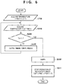
- FIG. 6 shows the operation of the image capturing system 30 .
- the operation shown in FIG. 6 can be controlled by the calculator 20 .
- the calculator 20 can be formed by, for example, a PLD (short for Programmable Logic Device) such as an FPGA (short for Field Programmable Gate Array) an ASIC (short for Application Specific Integrated Circuit), a general-purpose computer with a program installed, or a combination of all or some of them.
- a PLD short for Programmable Logic Device
- FPGA field Programmable Gate Array
- ASIC application Specific Integrated Circuit
- the image capturing apparatus 10 may be unable to normally operate.
- a threshold is set for use of the image capturing apparatus 10 , and if the temperature during use exceeds the threshold, a warning is output, and the image capturing apparatus 10 is stopped because the operation of the image capturing apparatus 10 may be abnormal.
- step S 200 the calculator 20 acquires a temperature threshold Tth.
- the temperature threshold Tth can be acquired from, for example, a nonvolatile memory.
- the nonvolatile memory may be provided in the calculator 20 or outside the calculator 20 .
- step S 210 the calculator 20 obtains a corrected temperature Ti according to equation (1) based on the temperature signal and the reference signal output from the image capturing apparatus 10 (signal processing circuit 105 ).
- the calculator 20 can obtain the corrected temperature Ti by obtaining the ratio of the temperature signal to the reference signal, as described above.
- step S 220 the calculator 20 compares the temperature Ti with the temperature threshold Tth. If the temperature Ti is equal to or lower than the threshold temperature Tth, in step S 230 , the calculator 20 causes the image capturing apparatus 10 to output an image signal for a period ⁇ t, and after that, returns to step S 210 . On the other hand, if the temperature Ti is higher than the threshold temperature Tth, the calculator 20 outputs a warning in step S 235 , and stops the operation of the image capturing apparatus 10 in step S 245 .
- the stop of the operation of the image capturing apparatus 10 is, for example, the stop of supply of the power supply voltage to the image capturing apparatus 10 or the stop of the image capturing operation.
- the processing shown in FIG. 5 can be started simultaneously with the start of the operation of the image capturing apparatus 10 .
- the processing shown in FIG. 5 may be activated by another apparatus.
- the image capturing system 30 includes an output unit such as a display unit and/or a speaker
- the warning output of step S 235 can be done by driving the output unit.
- the warning output of step S 235 may be done for a control unit or an output unit provided in a host system including the image capturing system 30 .
- the image capturing system 30 is mounted on a movable apparatus such as an automobile, a warning can be output from an output unit provided in the movable apparatus based on the warning output from the image capturing system 30 .
- the operation of the image capturing apparatus 10 is stopped after the output of the warning.
- the operation of the image capturing apparatus 10 need not always be stopped.
- the operation of the image capturing apparatus 10 may be stopped, and after that, a warning may be output.
- FIG. 7 shows the arrangement of an image capturing apparatus 10 according to the second embodiment of the present invention. Matters that are not mentioned as the second embodiment comply with the first embodiment.
- a calculator 20 is incorporated in the image capturing apparatus 10 .
- FIG. 8 shows the arrangement of an automobile 900 as an example of a movable apparatus incorporating the image capturing system 30 according to the first embodiment or the image capturing apparatus 10 according to the second embodiment.
- the automobile 900 includes an image capturing apparatus 902 corresponding to the image capturing system 30 according to the first embodiment or the image capturing apparatus 10 according to the second embodiment.
- the automobile 900 also includes an ASIC (Application Specific Integrated Circuit) 903 , a warning device 912 , and a main control unit 913 .
- ASIC Application Specific Integrated Circuit
- the warning device 912 Upon receiving a signal representing an abnormality from the image capturing apparatus 902 , a vehicle sensor, a control unit, or the like, the warning device 912 gives a warning to the driver.
- the main control unit 913 generally controls the operations of the image capturing apparatus 902 , the vehicle sensor, the control unit, and the like. Note that the automobile 900 need not always include the main control unit 913 . In this case, the image capturing apparatus 902 , the vehicle sensor, or the control unit transmits/receives a control signal via a communication network (for example, CAN standard).
- a communication network for example, CAN standard
- FIG. 9 is a block diagram showing the system arrangement of the automobile 900 .
- the automobile 900 includes the first image capturing apparatus 902 and the second image capturing apparatus 902 .
- a stereo camera is formed by the first image capturing apparatus 902 and the second image capturing apparatus 902 .
- An object image is formed on the image capturing apparatus 902 by an optical unit 914 .
- a pixel signal output from the image capturing apparatus 902 is processed by an image preprocessor 915 and transmitted to the ASIC 903 .
- the image preprocessor 915 performs calculation of obtaining the difference between the optical signal VS and the noise signal VN or processing such as synchronization signal addition.
- the ASIC 903 can include an image processor 904 , an optical distance measuring unit 906 , a parallax calculator 907 , an object recognition unit 908 , and an abnormality detection unit 909 .
- the image processor 904 processes the pixel signal to generate an image signal.
- the image processor 904 also performs correction of an image signal or defect compensation.
- the image processor 904 includes a memory 905 that temporarily holds the image signal.
- the memory 905 may store the position of a known defective pixel of the image capturing apparatus 902 .
- the above-described calculator 20 may be provided in the image processor 904 .
- the optical distance measuring unit 906 performs focusing or distance measurement of the object using the image signal.
- the parallax calculator 907 performs object collation (stereo matching) of a parallax image.
- the object recognition unit 908 analyzes the image signal and recognizes objects such as an automobile, a person, a signpost, and a road.
- the abnormality detection unit 909 detects a fault or an operation error of the image capturing apparatus 902 . Upon detecting a fault or an operation error, the abnormality detection unit 909 sends a signal representing detection of the abnormality to the main control unit 913 .
- the abnormality detection unit 909 may have the function of the above-described calculator 20 .
- the automobile 900 includes a vehicle sensor 910 and a driving support unit 911 .
- the vehicle sensor 910 can include a speed/acceleration sensor, an angular velocity sensor, a steering angle sensor, a ranging radar, and a pressure sensor.
- the driving support unit 911 includes a collision determination unit.
- the collision determination unit determines, based on pieces of information from the optical distance measuring unit 906 , the parallax calculator 907 , and the object recognition unit 908 , whether there is possibility of collision against an object.
- the optical distance measuring unit 906 and the parallax calculator 907 are examples of a distance information acquisition means for acquiring information of a distance to a target. That is, the distance information is information about a parallax, a defocus amount, and a distance up to the target.
- the collision determination unit may determine the collision possibility using one of these pieces of distance information.
- the distance information acquisition means may be implemented by hardware designed for a special purpose or may be implemented by a software module.
- the driving support unit 911 controls the automobile 900 so it does not collide against another object has been described. However, it is also applicable to control of automatic driving following another vehicle or control of automatic driving not to drive off a lane.
- the automobile 900 also includes driving units used for driving such as an air bag, an accelerator, a brake, a steering, and a transmission.
- the automobile 900 also includes control units for these units. Each control unit controls a corresponding driving unit based on a control signal of the main control unit 913 .
- the image capturing apparatus or the image capturing system When performing driving support or automatic driving by mounting, in the automobile 900 , the image capturing apparatus or the image capturing system according to the present invention, as described above, a plurality of image capturing apparatuses or image capturing systems can be used. At this time, if the characteristic of an element in the temperature signal output unit changes between the image capturing apparatuses or image capturing systems, an assumed temperature changes between the image capturing apparatuses, and it may be impossible to normally perform driving support or automatic driving. In addition, since driving support or automatic driving of the automobile 900 requires correctness, the accuracy required for temperature measurement is also high.
- the image capturing apparatus or image capturing system according to the present invention When the image capturing apparatus or image capturing system according to the present invention is used, the accuracy of temperature measurement can be improved, and the correctness of driving support or automatic driving can be increased.
- the image capturing system used in the embodiments is applicable not only to an automobile but also to, for example, a movable apparatus such as ship, an airplane, or an industrial robot.
- the image capturing system is also applicable not only to a movable apparatus but also widely to a device using object recognition such as an ITS (Intelligent Transportation System).
- Embodiment(s) of the present invention can also be realized by a computer of a system or apparatus that reads out and executes computer executable instructions (e.g., one or more programs) recorded on a storage medium (which may also be referred to more fully as a ‘non-transitory computer-readable storage medium’) to perform the functions of one or more of the above-described embodiment(s) and/or that includes one or more circuits (e.g., application specific integrated circuit (ASIC)) for performing the functions of one or more of the above-described embodiment(s), and by a method performed by the computer of the system or apparatus by, for example, reading out and executing the computer executable instructions from the storage medium to perform the functions of one or more of the above-described embodiment(s) and/or controlling the one or more circuits to perform the functions of one or more of the above-described embodiment(s).
- computer executable instructions e.g., one or more programs
- a storage medium which may also be referred to more fully as a
- the computer may comprise one or more processors (e.g., central processing unit (CPU), micro processing unit (MPU)) and may include a network of separate computers or separate processors to read out and execute the computer executable instructions.
- the computer executable instructions may be provided to the computer, for example, from a network or the storage medium.
- the storage medium may include, for example, one or more of a hard disk, a random-access memory (RAM), a read only memory (ROM), a storage of distributed computing systems, an optical disk (such as a compact disc (CD), digital versatile disc (DVD), or Blu-ray Disc (BD)TM), a flash memory device, a memory card, and the like.
Landscapes
- Engineering & Computer Science (AREA)
- Multimedia (AREA)
- Signal Processing (AREA)
- Physics & Mathematics (AREA)
- General Physics & Mathematics (AREA)
- Environmental & Geological Engineering (AREA)
- Transforming Light Signals Into Electric Signals (AREA)
- Solid State Image Pick-Up Elements (AREA)
- Radiation Pyrometers (AREA)
- Color Television Image Signal Generators (AREA)
Applications Claiming Priority (2)
| Application Number | Priority Date | Filing Date | Title |
|---|---|---|---|
| JP2016-194774 | 2016-09-30 | ||
| JP2016194774A JP6800682B2 (ja) | 2016-09-30 | 2016-09-30 | 撮像装置、撮像システムおよび移動体 |
Publications (2)
| Publication Number | Publication Date |
|---|---|
| US20180097960A1 US20180097960A1 (en) | 2018-04-05 |
| US10609243B2 true US10609243B2 (en) | 2020-03-31 |
Family
ID=59930172
Family Applications (1)
| Application Number | Title | Priority Date | Filing Date |
|---|---|---|---|
| US15/711,105 Active 2038-03-02 US10609243B2 (en) | 2016-09-30 | 2017-09-21 | Image capturing apparatus, image capturing system, and movable apparatus |
Country Status (4)
| Country | Link |
|---|---|
| US (1) | US10609243B2 (ja) |
| EP (2) | EP3313061B1 (ja) |
| JP (1) | JP6800682B2 (ja) |
| CN (1) | CN107888808B (ja) |
Cited By (4)
| Publication number | Priority date | Publication date | Assignee | Title |
|---|---|---|---|---|
| US11477401B2 (en) | 2020-02-28 | 2022-10-18 | Canon Kabushiki Kaisha | Imaging device and imaging system |
| US11496704B2 (en) | 2019-07-19 | 2022-11-08 | Canon Kabushiki Kaisha | Photoelectric conversion device having select circuit with a switch circuit having a plurality of switches, and imaging system |
| US11653114B2 (en) | 2019-07-19 | 2023-05-16 | Canon Kabushiki Kaisha | Photoelectric conversion device and imaging system |
| US11652983B2 (en) | 2017-01-25 | 2023-05-16 | Canon Kabushiki Kaisha | Solid-state imaging device, imaging system, and movable object |
Families Citing this family (10)
| Publication number | Priority date | Publication date | Assignee | Title |
|---|---|---|---|---|
| JP6800682B2 (ja) | 2016-09-30 | 2020-12-16 | キヤノン株式会社 | 撮像装置、撮像システムおよび移動体 |
| JP2019087939A (ja) | 2017-11-09 | 2019-06-06 | キヤノン株式会社 | 光電変換装置、電子機器、輸送機器および光電変換装置の駆動方法 |
| JP6704893B2 (ja) | 2017-11-30 | 2020-06-03 | キヤノン株式会社 | 固体撮像装置、撮像システム、および固体撮像装置の駆動方法 |
| JP7297433B2 (ja) | 2018-12-11 | 2023-06-26 | キヤノン株式会社 | 光電変換装置および撮像システム |
| JP7286309B2 (ja) * | 2018-12-18 | 2023-06-05 | キヤノン株式会社 | 光電変換装置、光電変換システムおよび信号処理装置 |
| CN113167656A (zh) * | 2019-01-10 | 2021-07-23 | 索尼半导体解决方案公司 | 成像装置和校准方法 |
| JP7299711B2 (ja) | 2019-01-30 | 2023-06-28 | キヤノン株式会社 | 光電変換装置及びその駆動方法 |
| JP2020201074A (ja) * | 2019-06-07 | 2020-12-17 | 株式会社村田製作所 | 温度検出回路及びモジュール |
| JP2022119383A (ja) * | 2021-02-04 | 2022-08-17 | キヤノン株式会社 | 光電変換装置、光電変換システム、半導体基板 |
| JP2022119384A (ja) | 2021-02-04 | 2022-08-17 | キヤノン株式会社 | 光電変換装置、光電変換システム、移動体 |
Citations (18)
| Publication number | Priority date | Publication date | Assignee | Title |
|---|---|---|---|---|
| JPH077667A (ja) | 1992-10-09 | 1995-01-10 | Nikon Corp | 赤外線撮像装置 |
| DE102004013269A1 (de) | 2004-03-18 | 2005-09-29 | Adc Automotive Distance Control Systems Gmbh | Verfahren zur Bestimmung der Temperatur eines Bildsensors |
| US7225099B1 (en) | 2005-02-10 | 2007-05-29 | Xilinx, Inc. | Apparatus and method for temperature measurement using a bandgap voltage reference |
| US20070273775A1 (en) | 2006-05-24 | 2007-11-29 | Jutao Jiang | Image sensor with built-in thermometer for global black level calibration and temperature-dependent color correction |
| JP2007329655A (ja) | 2006-06-07 | 2007-12-20 | Konica Minolta Holdings Inc | 撮像装置 |
| JP2008039451A (ja) | 2006-08-02 | 2008-02-21 | Sony Corp | 温度検出回路およびその試験方法、並びに半導体装置 |
| US7648271B2 (en) * | 2007-04-23 | 2010-01-19 | Texas Instruments Incorporated | Systems and methods for temperature measurement using n-factor coefficient correction |
| US7741593B2 (en) | 2008-02-13 | 2010-06-22 | Canon Kabushiki Kaisha | Photoelectric conversion device and imaging system |
| US20110205071A1 (en) * | 2010-02-24 | 2011-08-25 | Sony Corporation | Electronic apparatus and method of controlling electronic apparatus |
| US20120194718A1 (en) * | 2011-02-01 | 2012-08-02 | Kabushiki Kaisha Toshiba | Solid state imaging device |
| JP2012151664A (ja) | 2011-01-19 | 2012-08-09 | Toshiba Corp | 固体撮像装置 |
| US8289431B2 (en) | 2008-06-05 | 2012-10-16 | Canon Kabushiki Kaisha | Image sensing device and image sensing system |
| US20130049777A1 (en) | 2011-08-31 | 2013-02-28 | Shen Wang | Device identification and temperature sensor circuit |
| US8400546B2 (en) | 2009-05-18 | 2013-03-19 | Canon Kabushiki Kaisha | Image capturing device, image capturing system, and method of driving image capturing device |
| US8928786B2 (en) | 2011-10-07 | 2015-01-06 | Canon Kabushiki Kaisha | Solid-state imaging apparatus and method of driving the same |
| US9083906B2 (en) | 2011-09-15 | 2015-07-14 | Canon Kabushiki Kaisha | A/D converter and solid-state imaging apparatus with offset voltage correction |
| JP2016009880A (ja) | 2014-06-20 | 2016-01-18 | キヤノン株式会社 | 撮像装置、撮像方法及び撮像システム |
| US20170257605A1 (en) | 2016-03-01 | 2017-09-07 | Canon Kabushiki Kaisha | Imaging device, imaging system, and image processing method |
Family Cites Families (6)
| Publication number | Priority date | Publication date | Assignee | Title |
|---|---|---|---|---|
| JP2011188224A (ja) * | 2010-03-09 | 2011-09-22 | Sony Corp | 温度情報出力装置、撮像装置、温度情報出力方法 |
| WO2011132393A1 (ja) * | 2010-04-23 | 2011-10-27 | コニカミノルタオプト株式会社 | 撮像装置および撮像装置の温度特性補正方法 |
| KR101760816B1 (ko) * | 2010-10-28 | 2017-07-25 | 삼성전자주식회사 | 온도 센서, 이를 포함하는 장치 및 이미지 센싱 시스템 |
| JP2015198273A (ja) * | 2014-03-31 | 2015-11-09 | ソニー株式会社 | イメージセンサ、およびイメージセンサの動作方法、撮像装置および撮像方法、並びに電子機器 |
| DE102014106034B4 (de) * | 2014-04-30 | 2022-02-10 | Connaught Electronics Ltd. | Verfahren zum Versetzen eines Bildsensors einer Fahrzeugkamera eines Kraftfahrzeugs in einen Bildaufnahmezustand, Kamerasystem sowie Kraftfahrzeug |
| JP6800682B2 (ja) | 2016-09-30 | 2020-12-16 | キヤノン株式会社 | 撮像装置、撮像システムおよび移動体 |
-
2016
- 2016-09-30 JP JP2016194774A patent/JP6800682B2/ja active Active
-
2017
- 2017-09-15 EP EP17191219.9A patent/EP3313061B1/en active Active
- 2017-09-15 EP EP21202595.1A patent/EP3979625A1/en active Pending
- 2017-09-21 US US15/711,105 patent/US10609243B2/en active Active
- 2017-09-30 CN CN201710912841.3A patent/CN107888808B/zh active Active
Patent Citations (19)
| Publication number | Priority date | Publication date | Assignee | Title |
|---|---|---|---|---|
| JPH077667A (ja) | 1992-10-09 | 1995-01-10 | Nikon Corp | 赤外線撮像装置 |
| DE102004013269A1 (de) | 2004-03-18 | 2005-09-29 | Adc Automotive Distance Control Systems Gmbh | Verfahren zur Bestimmung der Temperatur eines Bildsensors |
| US7225099B1 (en) | 2005-02-10 | 2007-05-29 | Xilinx, Inc. | Apparatus and method for temperature measurement using a bandgap voltage reference |
| US20070273775A1 (en) | 2006-05-24 | 2007-11-29 | Jutao Jiang | Image sensor with built-in thermometer for global black level calibration and temperature-dependent color correction |
| JP2007329655A (ja) | 2006-06-07 | 2007-12-20 | Konica Minolta Holdings Inc | 撮像装置 |
| JP2008039451A (ja) | 2006-08-02 | 2008-02-21 | Sony Corp | 温度検出回路およびその試験方法、並びに半導体装置 |
| US7648271B2 (en) * | 2007-04-23 | 2010-01-19 | Texas Instruments Incorporated | Systems and methods for temperature measurement using n-factor coefficient correction |
| US7741593B2 (en) | 2008-02-13 | 2010-06-22 | Canon Kabushiki Kaisha | Photoelectric conversion device and imaging system |
| US8289431B2 (en) | 2008-06-05 | 2012-10-16 | Canon Kabushiki Kaisha | Image sensing device and image sensing system |
| US8400546B2 (en) | 2009-05-18 | 2013-03-19 | Canon Kabushiki Kaisha | Image capturing device, image capturing system, and method of driving image capturing device |
| US20110205071A1 (en) * | 2010-02-24 | 2011-08-25 | Sony Corporation | Electronic apparatus and method of controlling electronic apparatus |
| JP2012151664A (ja) | 2011-01-19 | 2012-08-09 | Toshiba Corp | 固体撮像装置 |
| US9154718B2 (en) | 2011-01-19 | 2015-10-06 | Kabushiki Kaisha Toshiba | Solid state imaging device |
| US20120194718A1 (en) * | 2011-02-01 | 2012-08-02 | Kabushiki Kaisha Toshiba | Solid state imaging device |
| US20130049777A1 (en) | 2011-08-31 | 2013-02-28 | Shen Wang | Device identification and temperature sensor circuit |
| US9083906B2 (en) | 2011-09-15 | 2015-07-14 | Canon Kabushiki Kaisha | A/D converter and solid-state imaging apparatus with offset voltage correction |
| US8928786B2 (en) | 2011-10-07 | 2015-01-06 | Canon Kabushiki Kaisha | Solid-state imaging apparatus and method of driving the same |
| JP2016009880A (ja) | 2014-06-20 | 2016-01-18 | キヤノン株式会社 | 撮像装置、撮像方法及び撮像システム |
| US20170257605A1 (en) | 2016-03-01 | 2017-09-07 | Canon Kabushiki Kaisha | Imaging device, imaging system, and image processing method |
Non-Patent Citations (2)
| Title |
|---|
| Search Report dated Jul. 11, 2018, in European Patent Application No. 17191219.9. |
| Search Report dated Mar. 12, 2018, in European Patent Application No. 17191219.9. |
Cited By (4)
| Publication number | Priority date | Publication date | Assignee | Title |
|---|---|---|---|---|
| US11652983B2 (en) | 2017-01-25 | 2023-05-16 | Canon Kabushiki Kaisha | Solid-state imaging device, imaging system, and movable object |
| US11496704B2 (en) | 2019-07-19 | 2022-11-08 | Canon Kabushiki Kaisha | Photoelectric conversion device having select circuit with a switch circuit having a plurality of switches, and imaging system |
| US11653114B2 (en) | 2019-07-19 | 2023-05-16 | Canon Kabushiki Kaisha | Photoelectric conversion device and imaging system |
| US11477401B2 (en) | 2020-02-28 | 2022-10-18 | Canon Kabushiki Kaisha | Imaging device and imaging system |
Also Published As
| Publication number | Publication date |
|---|---|
| EP3979625A1 (en) | 2022-04-06 |
| US20180097960A1 (en) | 2018-04-05 |
| JP6800682B2 (ja) | 2020-12-16 |
| JP2018056970A (ja) | 2018-04-05 |
| EP3313061A2 (en) | 2018-04-25 |
| EP3313061A3 (en) | 2018-08-08 |
| CN107888808B (zh) | 2021-01-26 |
| CN107888808A (zh) | 2018-04-06 |
| EP3313061B1 (en) | 2021-11-24 |
Similar Documents
| Publication | Publication Date | Title |
|---|---|---|
| US10609243B2 (en) | Image capturing apparatus, image capturing system, and movable apparatus | |
| US11431929B2 (en) | Photoelectric conversion device and equipment | |
| CN108259789B (zh) | 固态成像设备 | |
| US10841517B2 (en) | Solid-state imaging device and imaging system | |
| US11140345B2 (en) | Solid state imaging device, imaging system, and drive method of solid state imaging device | |
| US20180213219A1 (en) | Solid-state imaging device, imaging system, and movable object | |
| US20220021827A1 (en) | Photoelectric conversion device and image sensing system | |
| US9894300B2 (en) | Image sensing device for measuring temperature without temperature sensor and method for driving the same | |
| US10401217B2 (en) | Data output device | |
| US20190349540A1 (en) | Imaging device and method of driving imaging device | |
| US10841519B2 (en) | Photoelectric conversion apparatus, equipment, and driving method of photoelectric conversion apparatus | |
| US20240022838A1 (en) | Photoelectric conversion apparatus and system | |
| US20220286100A1 (en) | Comparator, photoelectric conversion device, and apparatus | |
| JP7145925B2 (ja) | 撮像システムおよび移動体 | |
| JP7316049B2 (ja) | 光電変換装置及び光電変換システム | |
| US20230179893A1 (en) | Photoelectric conversion device | |
| JP7361582B2 (ja) | 光電変換装置、光電変換システムおよび輸送機器 | |
| US20230179881A1 (en) | Photoelectric conversion device | |
| US10560650B2 (en) | Photoelectric conversion device | |
| US11310456B2 (en) | Photoelectric conversion device and imaging system | |
| US20230237960A1 (en) | Semiconductor device | |
| US11832012B2 (en) | Photoelectric conversion device | |
| US20220115366A1 (en) | Photoelectric conversion apparatus, photo-detection system, and movable body | |
| US11838664B2 (en) | Semiconductor device, system, and device using the same |
Legal Events
| Date | Code | Title | Description |
|---|---|---|---|
| FEPP | Fee payment procedure |
Free format text: ENTITY STATUS SET TO UNDISCOUNTED (ORIGINAL EVENT CODE: BIG.); ENTITY STATUS OF PATENT OWNER: LARGE ENTITY |
|
| STPP | Information on status: patent application and granting procedure in general |
Free format text: DOCKETED NEW CASE - READY FOR EXAMINATION |
|
| AS | Assignment |
Owner name: CANON KABUSHIKI KAISHA, JAPAN Free format text: ASSIGNMENT OF ASSIGNORS INTEREST;ASSIGNORS:OCHIAI, KEI;SHIRAI, TAKAHIRO;ITANO, TETSUYA;AND OTHERS;REEL/FRAME:044835/0136 Effective date: 20170911 |
|
| STPP | Information on status: patent application and granting procedure in general |
Free format text: NON FINAL ACTION MAILED |
|
| STPP | Information on status: patent application and granting procedure in general |
Free format text: RESPONSE TO NON-FINAL OFFICE ACTION ENTERED AND FORWARDED TO EXAMINER |
|
| STPP | Information on status: patent application and granting procedure in general |
Free format text: NOTICE OF ALLOWANCE MAILED -- APPLICATION RECEIVED IN OFFICE OF PUBLICATIONS |
|
| STPP | Information on status: patent application and granting procedure in general |
Free format text: PUBLICATIONS -- ISSUE FEE PAYMENT VERIFIED |
|
| STCF | Information on status: patent grant |
Free format text: PATENTED CASE |
|
| MAFP | Maintenance fee payment |
Free format text: PAYMENT OF MAINTENANCE FEE, 4TH YEAR, LARGE ENTITY (ORIGINAL EVENT CODE: M1551); ENTITY STATUS OF PATENT OWNER: LARGE ENTITY Year of fee payment: 4 |