US10312252B2 - Method of manufacturing semiconductor device - Google Patents
Method of manufacturing semiconductor device Download PDFInfo
- Publication number
- US10312252B2 US10312252B2 US15/486,741 US201715486741A US10312252B2 US 10312252 B2 US10312252 B2 US 10312252B2 US 201715486741 A US201715486741 A US 201715486741A US 10312252 B2 US10312252 B2 US 10312252B2
- Authority
- US
- United States
- Prior art keywords
- region
- gate electrode
- diffusion layer
- semiconductor substrate
- diffusion
- Prior art date
- Legal status (The legal status is an assumption and is not a legal conclusion. Google has not performed a legal analysis and makes no representation as to the accuracy of the status listed.)
- Active, expires
Links
- 239000004065 semiconductor Substances 0.000 title claims abstract description 258
- 238000004519 manufacturing process Methods 0.000 title claims abstract description 70
- 238000009792 diffusion process Methods 0.000 claims abstract description 279
- 230000015654 memory Effects 0.000 claims abstract description 217
- 239000012535 impurity Substances 0.000 claims abstract description 118
- 238000010438 heat treatment Methods 0.000 claims abstract description 19
- 239000000758 substrate Substances 0.000 claims description 132
- 238000009825 accumulation Methods 0.000 claims description 10
- 230000005669 field effect Effects 0.000 claims description 7
- 230000015572 biosynthetic process Effects 0.000 abstract description 40
- 238000000034 method Methods 0.000 abstract description 39
- 125000001475 halogen functional group Chemical group 0.000 abstract description 36
- 238000005468 ion implantation Methods 0.000 abstract description 21
- LPQOADBMXVRBNX-UHFFFAOYSA-N ac1ldcw0 Chemical compound Cl.C1CN(C)CCN1C1=C(F)C=C2C(=O)C(C(O)=O)=CN3CCSC1=C32 LPQOADBMXVRBNX-UHFFFAOYSA-N 0.000 abstract 2
- 239000010410 layer Substances 0.000 description 165
- 229910052581 Si3N4 Inorganic materials 0.000 description 52
- 229920002120 photoresistant polymer Polymers 0.000 description 52
- HQVNEWCFYHHQES-UHFFFAOYSA-N silicon nitride Chemical compound N12[Si]34N5[Si]62N3[Si]51N64 HQVNEWCFYHHQES-UHFFFAOYSA-N 0.000 description 52
- 229910052710 silicon Inorganic materials 0.000 description 45
- 239000010703 silicon Substances 0.000 description 45
- XUIMIQQOPSSXEZ-UHFFFAOYSA-N Silicon Chemical compound [Si] XUIMIQQOPSSXEZ-UHFFFAOYSA-N 0.000 description 42
- VYPSYNLAJGMNEJ-UHFFFAOYSA-N Silicium dioxide Chemical compound O=[Si]=O VYPSYNLAJGMNEJ-UHFFFAOYSA-N 0.000 description 37
- 229910052814 silicon oxide Inorganic materials 0.000 description 36
- 230000000052 comparative effect Effects 0.000 description 23
- 239000011229 interlayer Substances 0.000 description 12
- 229910052785 arsenic Inorganic materials 0.000 description 11
- RQNWIZPPADIBDY-UHFFFAOYSA-N arsenic atom Chemical compound [As] RQNWIZPPADIBDY-UHFFFAOYSA-N 0.000 description 11
- 238000005229 chemical vapour deposition Methods 0.000 description 11
- 230000007423 decrease Effects 0.000 description 10
- BHEPBYXIRTUNPN-UHFFFAOYSA-N hydridophosphorus(.) (triplet) Chemical compound [PH] BHEPBYXIRTUNPN-UHFFFAOYSA-N 0.000 description 10
- 238000003860 storage Methods 0.000 description 9
- 230000015556 catabolic process Effects 0.000 description 8
- 230000003247 decreasing effect Effects 0.000 description 8
- 238000002955 isolation Methods 0.000 description 8
- 239000004020 conductor Substances 0.000 description 7
- 238000005530 etching Methods 0.000 description 7
- 229910021332 silicide Inorganic materials 0.000 description 7
- FVBUAEGBCNSCDD-UHFFFAOYSA-N silicide(4-) Chemical compound [Si-4] FVBUAEGBCNSCDD-UHFFFAOYSA-N 0.000 description 7
- 239000000969 carrier Substances 0.000 description 6
- 230000000694 effects Effects 0.000 description 6
- 238000002513 implantation Methods 0.000 description 6
- 238000002347 injection Methods 0.000 description 6
- 239000007924 injection Substances 0.000 description 6
- 229910052751 metal Inorganic materials 0.000 description 6
- 239000002184 metal Substances 0.000 description 6
- 230000006870 function Effects 0.000 description 5
- 229910044991 metal oxide Inorganic materials 0.000 description 5
- 238000007254 oxidation reaction Methods 0.000 description 5
- 230000004888 barrier function Effects 0.000 description 4
- 238000000151 deposition Methods 0.000 description 4
- 150000004706 metal oxides Chemical class 0.000 description 4
- 230000003647 oxidation Effects 0.000 description 4
- PXHVJJICTQNCMI-UHFFFAOYSA-N Nickel Chemical compound [Ni] PXHVJJICTQNCMI-UHFFFAOYSA-N 0.000 description 3
- 238000004140 cleaning Methods 0.000 description 3
- 230000005684 electric field Effects 0.000 description 3
- 239000012212 insulator Substances 0.000 description 3
- 150000002500 ions Chemical class 0.000 description 3
- ZOXJGFHDIHLPTG-UHFFFAOYSA-N Boron Chemical compound [B] ZOXJGFHDIHLPTG-UHFFFAOYSA-N 0.000 description 2
- KRHYYFGTRYWZRS-UHFFFAOYSA-N Fluorane Chemical compound F KRHYYFGTRYWZRS-UHFFFAOYSA-N 0.000 description 2
- OAICVXFJPJFONN-UHFFFAOYSA-N Phosphorus Chemical compound [P] OAICVXFJPJFONN-UHFFFAOYSA-N 0.000 description 2
- 229910021417 amorphous silicon Inorganic materials 0.000 description 2
- 229910052796 boron Inorganic materials 0.000 description 2
- 230000005465 channeling Effects 0.000 description 2
- 239000010949 copper Substances 0.000 description 2
- 238000002425 crystallisation Methods 0.000 description 2
- 230000008025 crystallization Effects 0.000 description 2
- 238000001312 dry etching Methods 0.000 description 2
- 229910000449 hafnium oxide Inorganic materials 0.000 description 2
- WIHZLLGSGQNAGK-UHFFFAOYSA-N hafnium(4+);oxygen(2-) Chemical compound [O-2].[O-2].[Hf+4] WIHZLLGSGQNAGK-UHFFFAOYSA-N 0.000 description 2
- 238000003475 lamination Methods 0.000 description 2
- TWNQGVIAIRXVLR-UHFFFAOYSA-N oxo(oxoalumanyloxy)alumane Chemical compound O=[Al]O[Al]=O TWNQGVIAIRXVLR-UHFFFAOYSA-N 0.000 description 2
- BPUBBGLMJRNUCC-UHFFFAOYSA-N oxygen(2-);tantalum(5+) Chemical compound [O-2].[O-2].[O-2].[O-2].[O-2].[Ta+5].[Ta+5] BPUBBGLMJRNUCC-UHFFFAOYSA-N 0.000 description 2
- 229910052698 phosphorus Inorganic materials 0.000 description 2
- 239000011574 phosphorus Substances 0.000 description 2
- 229910021420 polycrystalline silicon Inorganic materials 0.000 description 2
- 238000005036 potential barrier Methods 0.000 description 2
- 230000008569 process Effects 0.000 description 2
- 239000002356 single layer Substances 0.000 description 2
- 125000006850 spacer group Chemical group 0.000 description 2
- 229910001936 tantalum oxide Inorganic materials 0.000 description 2
- 239000010936 titanium Substances 0.000 description 2
- WFKWXMTUELFFGS-UHFFFAOYSA-N tungsten Chemical compound [W] WFKWXMTUELFFGS-UHFFFAOYSA-N 0.000 description 2
- 229910052721 tungsten Inorganic materials 0.000 description 2
- 239000010937 tungsten Substances 0.000 description 2
- RYGMFSIKBFXOCR-UHFFFAOYSA-N Copper Chemical compound [Cu] RYGMFSIKBFXOCR-UHFFFAOYSA-N 0.000 description 1
- -1 Metal Oxide Nitride Chemical class 0.000 description 1
- RTAQQCXQSZGOHL-UHFFFAOYSA-N Titanium Chemical compound [Ti] RTAQQCXQSZGOHL-UHFFFAOYSA-N 0.000 description 1
- NRTOMJZYCJJWKI-UHFFFAOYSA-N Titanium nitride Chemical compound [Ti]#N NRTOMJZYCJJWKI-UHFFFAOYSA-N 0.000 description 1
- 230000001133 acceleration Effects 0.000 description 1
- 230000004913 activation Effects 0.000 description 1
- PNEYBMLMFCGWSK-UHFFFAOYSA-N aluminium oxide Inorganic materials [O-2].[O-2].[O-2].[Al+3].[Al+3] PNEYBMLMFCGWSK-UHFFFAOYSA-N 0.000 description 1
- 239000010941 cobalt Substances 0.000 description 1
- 229910017052 cobalt Inorganic materials 0.000 description 1
- GUTLYIVDDKVIGB-UHFFFAOYSA-N cobalt atom Chemical compound [Co] GUTLYIVDDKVIGB-UHFFFAOYSA-N 0.000 description 1
- 229910052802 copper Inorganic materials 0.000 description 1
- 238000009826 distribution Methods 0.000 description 1
- 238000000605 extraction Methods 0.000 description 1
- 230000006872 improvement Effects 0.000 description 1
- 238000011065 in-situ storage Methods 0.000 description 1
- 229910021421 monocrystalline silicon Inorganic materials 0.000 description 1
- 229910052759 nickel Inorganic materials 0.000 description 1
- 150000004767 nitrides Chemical class 0.000 description 1
- 230000001590 oxidative effect Effects 0.000 description 1
- 238000005498 polishing Methods 0.000 description 1
- 150000003376 silicon Chemical class 0.000 description 1
- 238000003892 spreading Methods 0.000 description 1
- 230000007480 spreading Effects 0.000 description 1
- 238000004544 sputter deposition Methods 0.000 description 1
- 239000000126 substance Substances 0.000 description 1
- 230000001629 suppression Effects 0.000 description 1
- 229910052719 titanium Inorganic materials 0.000 description 1
- 230000005641 tunneling Effects 0.000 description 1
Images


Classifications
-
- H01L27/11568—
-
- H—ELECTRICITY
- H10—SEMICONDUCTOR DEVICES; ELECTRIC SOLID-STATE DEVICES NOT OTHERWISE PROVIDED FOR
- H10B—ELECTRONIC MEMORY DEVICES
- H10B43/00—EEPROM devices comprising charge-trapping gate insulators
- H10B43/30—EEPROM devices comprising charge-trapping gate insulators characterised by the memory core region
-
- H—ELECTRICITY
- H01—ELECTRIC ELEMENTS
- H01L—SEMICONDUCTOR DEVICES NOT COVERED BY CLASS H10
- H01L21/00—Processes or apparatus adapted for the manufacture or treatment of semiconductor or solid state devices or of parts thereof
- H01L21/02—Manufacture or treatment of semiconductor devices or of parts thereof
- H01L21/04—Manufacture or treatment of semiconductor devices or of parts thereof the devices having at least one potential-jump barrier or surface barrier, e.g. PN junction, depletion layer or carrier concentration layer
- H01L21/18—Manufacture or treatment of semiconductor devices or of parts thereof the devices having at least one potential-jump barrier or surface barrier, e.g. PN junction, depletion layer or carrier concentration layer the devices having semiconductor bodies comprising elements of Group IV of the Periodic System or AIIIBV compounds with or without impurities, e.g. doping materials
- H01L21/26—Bombardment with radiation
- H01L21/263—Bombardment with radiation with high-energy radiation
- H01L21/265—Bombardment with radiation with high-energy radiation producing ion implantation
- H01L21/26506—Bombardment with radiation with high-energy radiation producing ion implantation in group IV semiconductors
- H01L21/26513—Bombardment with radiation with high-energy radiation producing ion implantation in group IV semiconductors of electrically active species
-
- H—ELECTRICITY
- H01—ELECTRIC ELEMENTS
- H01L—SEMICONDUCTOR DEVICES NOT COVERED BY CLASS H10
- H01L21/00—Processes or apparatus adapted for the manufacture or treatment of semiconductor or solid state devices or of parts thereof
- H01L21/02—Manufacture or treatment of semiconductor devices or of parts thereof
- H01L21/04—Manufacture or treatment of semiconductor devices or of parts thereof the devices having at least one potential-jump barrier or surface barrier, e.g. PN junction, depletion layer or carrier concentration layer
- H01L21/18—Manufacture or treatment of semiconductor devices or of parts thereof the devices having at least one potential-jump barrier or surface barrier, e.g. PN junction, depletion layer or carrier concentration layer the devices having semiconductor bodies comprising elements of Group IV of the Periodic System or AIIIBV compounds with or without impurities, e.g. doping materials
- H01L21/28—Manufacture of electrodes on semiconductor bodies using processes or apparatus not provided for in groups H01L21/20 - H01L21/268
- H01L21/28008—Making conductor-insulator-semiconductor electrodes
-
- H—ELECTRICITY
- H01—ELECTRIC ELEMENTS
- H01L—SEMICONDUCTOR DEVICES NOT COVERED BY CLASS H10
- H01L21/00—Processes or apparatus adapted for the manufacture or treatment of semiconductor or solid state devices or of parts thereof
- H01L21/02—Manufacture or treatment of semiconductor devices or of parts thereof
- H01L21/04—Manufacture or treatment of semiconductor devices or of parts thereof the devices having at least one potential-jump barrier or surface barrier, e.g. PN junction, depletion layer or carrier concentration layer
- H01L21/18—Manufacture or treatment of semiconductor devices or of parts thereof the devices having at least one potential-jump barrier or surface barrier, e.g. PN junction, depletion layer or carrier concentration layer the devices having semiconductor bodies comprising elements of Group IV of the Periodic System or AIIIBV compounds with or without impurities, e.g. doping materials
- H01L21/30—Treatment of semiconductor bodies using processes or apparatus not provided for in groups H01L21/20 - H01L21/26
- H01L21/324—Thermal treatment for modifying the properties of semiconductor bodies, e.g. annealing, sintering
-
- H01L27/11573—
-
- H—ELECTRICITY
- H01—ELECTRIC ELEMENTS
- H01L—SEMICONDUCTOR DEVICES NOT COVERED BY CLASS H10
- H01L29/00—Semiconductor devices adapted for rectifying, amplifying, oscillating or switching, or capacitors or resistors with at least one potential-jump barrier or surface barrier, e.g. PN junction depletion layer or carrier concentration layer; Details of semiconductor bodies or of electrodes thereof ; Multistep manufacturing processes therefor
- H01L29/02—Semiconductor bodies ; Multistep manufacturing processes therefor
- H01L29/06—Semiconductor bodies ; Multistep manufacturing processes therefor characterised by their shape; characterised by the shapes, relative sizes, or dispositions of the semiconductor regions ; characterised by the concentration or distribution of impurities within semiconductor regions
- H01L29/08—Semiconductor bodies ; Multistep manufacturing processes therefor characterised by their shape; characterised by the shapes, relative sizes, or dispositions of the semiconductor regions ; characterised by the concentration or distribution of impurities within semiconductor regions with semiconductor regions connected to an electrode carrying current to be rectified, amplified or switched and such electrode being part of a semiconductor device which comprises three or more electrodes
- H01L29/0843—Source or drain regions of field-effect devices
- H01L29/0847—Source or drain regions of field-effect devices of field-effect transistors with insulated gate
-
- H—ELECTRICITY
- H01—ELECTRIC ELEMENTS
- H01L—SEMICONDUCTOR DEVICES NOT COVERED BY CLASS H10
- H01L29/00—Semiconductor devices adapted for rectifying, amplifying, oscillating or switching, or capacitors or resistors with at least one potential-jump barrier or surface barrier, e.g. PN junction depletion layer or carrier concentration layer; Details of semiconductor bodies or of electrodes thereof ; Multistep manufacturing processes therefor
- H01L29/40—Electrodes ; Multistep manufacturing processes therefor
- H01L29/41—Electrodes ; Multistep manufacturing processes therefor characterised by their shape, relative sizes or dispositions
- H01L29/423—Electrodes ; Multistep manufacturing processes therefor characterised by their shape, relative sizes or dispositions not carrying the current to be rectified, amplified or switched
- H01L29/42312—Gate electrodes for field effect devices
- H01L29/42316—Gate electrodes for field effect devices for field-effect transistors
- H01L29/4232—Gate electrodes for field effect devices for field-effect transistors with insulated gate
- H01L29/4234—Gate electrodes for transistors with charge trapping gate insulator
- H01L29/42344—Gate electrodes for transistors with charge trapping gate insulator with at least one additional gate, e.g. program gate, erase gate or select gate
-
- H—ELECTRICITY
- H01—ELECTRIC ELEMENTS
- H01L—SEMICONDUCTOR DEVICES NOT COVERED BY CLASS H10
- H01L29/00—Semiconductor devices adapted for rectifying, amplifying, oscillating or switching, or capacitors or resistors with at least one potential-jump barrier or surface barrier, e.g. PN junction depletion layer or carrier concentration layer; Details of semiconductor bodies or of electrodes thereof ; Multistep manufacturing processes therefor
- H01L29/66—Types of semiconductor device ; Multistep manufacturing processes therefor
- H01L29/66007—Multistep manufacturing processes
- H01L29/66075—Multistep manufacturing processes of devices having semiconductor bodies comprising group 14 or group 13/15 materials
- H01L29/66227—Multistep manufacturing processes of devices having semiconductor bodies comprising group 14 or group 13/15 materials the devices being controllable only by the electric current supplied or the electric potential applied, to an electrode which does not carry the current to be rectified, amplified or switched, e.g. three-terminal devices
- H01L29/66409—Unipolar field-effect transistors
- H01L29/66477—Unipolar field-effect transistors with an insulated gate, i.e. MISFET
- H01L29/66568—Lateral single gate silicon transistors
-
- H—ELECTRICITY
- H10—SEMICONDUCTOR DEVICES; ELECTRIC SOLID-STATE DEVICES NOT OTHERWISE PROVIDED FOR
- H10B—ELECTRONIC MEMORY DEVICES
- H10B43/00—EEPROM devices comprising charge-trapping gate insulators
- H10B43/40—EEPROM devices comprising charge-trapping gate insulators characterised by the peripheral circuit region
-
- H01L21/28282—
-
- H—ELECTRICITY
- H01—ELECTRIC ELEMENTS
- H01L—SEMICONDUCTOR DEVICES NOT COVERED BY CLASS H10
- H01L29/00—Semiconductor devices adapted for rectifying, amplifying, oscillating or switching, or capacitors or resistors with at least one potential-jump barrier or surface barrier, e.g. PN junction depletion layer or carrier concentration layer; Details of semiconductor bodies or of electrodes thereof ; Multistep manufacturing processes therefor
- H01L29/40—Electrodes ; Multistep manufacturing processes therefor
- H01L29/401—Multistep manufacturing processes
- H01L29/4011—Multistep manufacturing processes for data storage electrodes
- H01L29/40117—Multistep manufacturing processes for data storage electrodes the electrodes comprising a charge-trapping insulator
-
- H—ELECTRICITY
- H01—ELECTRIC ELEMENTS
- H01L—SEMICONDUCTOR DEVICES NOT COVERED BY CLASS H10
- H01L29/00—Semiconductor devices adapted for rectifying, amplifying, oscillating or switching, or capacitors or resistors with at least one potential-jump barrier or surface barrier, e.g. PN junction depletion layer or carrier concentration layer; Details of semiconductor bodies or of electrodes thereof ; Multistep manufacturing processes therefor
- H01L29/66—Types of semiconductor device ; Multistep manufacturing processes therefor
- H01L29/66007—Multistep manufacturing processes
- H01L29/66075—Multistep manufacturing processes of devices having semiconductor bodies comprising group 14 or group 13/15 materials
- H01L29/66227—Multistep manufacturing processes of devices having semiconductor bodies comprising group 14 or group 13/15 materials the devices being controllable only by the electric current supplied or the electric potential applied, to an electrode which does not carry the current to be rectified, amplified or switched, e.g. three-terminal devices
- H01L29/66409—Unipolar field-effect transistors
- H01L29/66477—Unipolar field-effect transistors with an insulated gate, i.e. MISFET
- H01L29/665—Unipolar field-effect transistors with an insulated gate, i.e. MISFET using self aligned silicidation, i.e. salicide
-
- H—ELECTRICITY
- H01—ELECTRIC ELEMENTS
- H01L—SEMICONDUCTOR DEVICES NOT COVERED BY CLASS H10
- H01L29/00—Semiconductor devices adapted for rectifying, amplifying, oscillating or switching, or capacitors or resistors with at least one potential-jump barrier or surface barrier, e.g. PN junction depletion layer or carrier concentration layer; Details of semiconductor bodies or of electrodes thereof ; Multistep manufacturing processes therefor
- H01L29/66—Types of semiconductor device ; Multistep manufacturing processes therefor
- H01L29/66007—Multistep manufacturing processes
- H01L29/66075—Multistep manufacturing processes of devices having semiconductor bodies comprising group 14 or group 13/15 materials
- H01L29/66227—Multistep manufacturing processes of devices having semiconductor bodies comprising group 14 or group 13/15 materials the devices being controllable only by the electric current supplied or the electric potential applied, to an electrode which does not carry the current to be rectified, amplified or switched, e.g. three-terminal devices
- H01L29/66409—Unipolar field-effect transistors
- H01L29/66477—Unipolar field-effect transistors with an insulated gate, i.e. MISFET
- H01L29/66568—Lateral single gate silicon transistors
- H01L29/66575—Lateral single gate silicon transistors where the source and drain or source and drain extensions are self-aligned to the sides of the gate
- H01L29/6659—Lateral single gate silicon transistors where the source and drain or source and drain extensions are self-aligned to the sides of the gate with both lightly doped source and drain extensions and source and drain self-aligned to the sides of the gate, e.g. lightly doped drain [LDD] MOSFET, double diffused drain [DDD] MOSFET
-
- H—ELECTRICITY
- H01—ELECTRIC ELEMENTS
- H01L—SEMICONDUCTOR DEVICES NOT COVERED BY CLASS H10
- H01L29/00—Semiconductor devices adapted for rectifying, amplifying, oscillating or switching, or capacitors or resistors with at least one potential-jump barrier or surface barrier, e.g. PN junction depletion layer or carrier concentration layer; Details of semiconductor bodies or of electrodes thereof ; Multistep manufacturing processes therefor
- H01L29/66—Types of semiconductor device ; Multistep manufacturing processes therefor
- H01L29/66007—Multistep manufacturing processes
- H01L29/66075—Multistep manufacturing processes of devices having semiconductor bodies comprising group 14 or group 13/15 materials
- H01L29/66227—Multistep manufacturing processes of devices having semiconductor bodies comprising group 14 or group 13/15 materials the devices being controllable only by the electric current supplied or the electric potential applied, to an electrode which does not carry the current to be rectified, amplified or switched, e.g. three-terminal devices
- H01L29/66409—Unipolar field-effect transistors
- H01L29/66477—Unipolar field-effect transistors with an insulated gate, i.e. MISFET
- H01L29/66833—Unipolar field-effect transistors with an insulated gate, i.e. MISFET with a charge trapping gate insulator, e.g. MNOS transistors
-
- H—ELECTRICITY
- H01—ELECTRIC ELEMENTS
- H01L—SEMICONDUCTOR DEVICES NOT COVERED BY CLASS H10
- H01L29/00—Semiconductor devices adapted for rectifying, amplifying, oscillating or switching, or capacitors or resistors with at least one potential-jump barrier or surface barrier, e.g. PN junction depletion layer or carrier concentration layer; Details of semiconductor bodies or of electrodes thereof ; Multistep manufacturing processes therefor
- H01L29/66—Types of semiconductor device ; Multistep manufacturing processes therefor
- H01L29/68—Types of semiconductor device ; Multistep manufacturing processes therefor controllable by only the electric current supplied, or only the electric potential applied, to an electrode which does not carry the current to be rectified, amplified or switched
- H01L29/76—Unipolar devices, e.g. field effect transistors
- H01L29/772—Field effect transistors
- H01L29/78—Field effect transistors with field effect produced by an insulated gate
- H01L29/792—Field effect transistors with field effect produced by an insulated gate with charge trapping gate insulator, e.g. MNOS-memory transistors
Definitions
- the present invention relates to a method of manufacturing a semiconductor device and for example, to a method of manufacturing a semiconductor device having a nonvolatile memory.
- EEPROMs Electrically Erasable and Programmable Read Only memories
- Such storage devices typified by flash memories which are widely used at present, have a conductive floating gate electrode surrounded by an oxide film or trap insulating film under the gate electrode of a MISFET, in which the state of charge storage in the floating gate or trap insulating film is taken as storage information and read as a transistor threshold.
- the trap insulating film refers to an insulating film which can store a charge and one such example is a silicon nitride film.
- the threshold of the MISFET is shifted by charge injection into, or charge emission from, such charge storage region so that the MISFET operates as a storage element.
- the nonvolatile semiconductor storage devices which use a trap insulating film are split-gate cells which use a MONOS (Metal Oxide Nitride Oxide Semiconductor) film.
- MONOS Metal Oxide Nitride Oxide Semiconductor
- the source and drain regions have an LDD structure which includes a semiconductor region with a low impurity concentration and a semiconductor region with a high impurity concentration.
- Japanese Unexamined Patent Application Publication No. 2008-153567 describes that a MOSFET (Metal Oxide Semiconductor Field Effect Transistor) is formed over a SOI (Silicon On Insulator) substrate.
- MOSFET Metal Oxide Semiconductor Field Effect Transistor
- SOI Silicon On Insulator
- Japanese Unexamined Patent Application Publication No. 1999-144483 describes that in a memory cell as a MOS (Metal Oxide Semiconductor) transistor, the drain region extends more widely than the source region.
- MOS Metal Oxide Semiconductor
- a method of manufacturing a semiconductor device which includes the steps of making a memory cell with a halo region on the drain region side for a split-gate MONOS memory, in which the source region of the memory cell has a larger depth than its drain region.
- the performance of the semiconductor device is enhanced.
- FIG. 1 is a sectional view of a step in a semiconductor device manufacturing process according to a first embodiment of the present invention
- FIG. 2 is a sectional view of a step next to the step shown in FIG. 1 in the semiconductor device manufacturing process
- FIG. 3 is a sectional view of a step next to the step shown in FIG. 2 in the semiconductor device manufacturing process
- FIG. 4 is a sectional view of a step next to the step shown in FIG. 3 in the semiconductor device manufacturing process
- FIG. 5 is a sectional view of a step next to the step shown in FIG. 4 in the semiconductor device manufacturing process
- FIG. 6 is a sectional view of a step next to the step shown in FIG. 5 in the semiconductor device manufacturing process
- FIG. 7 is a sectional view of a step next to the step shown in FIG. 6 in the semiconductor device manufacturing process
- FIG. 8 is a sectional view of a step next to the step shown in FIG. 7 in the semiconductor device manufacturing process
- FIG. 9 is a sectional view of a step next to the step shown in FIG. 8 in the semiconductor device manufacturing process.
- FIG. 10 is a sectional view of a step next to the step shown in FIG. 9 in the semiconductor device manufacturing process
- FIG. 11 is a sectional view of a step next to the step shown in FIG. 10 in the semiconductor device manufacturing process
- FIG. 12 is a sectional view of a step next to the step shown in FIG. 11 in the semiconductor device manufacturing process
- FIG. 13 is a sectional view of a step next to the step shown in FIG. 12 in the semiconductor device manufacturing process
- FIG. 14 is a sectional view of a step next to the step shown in FIG. 13 in the semiconductor device manufacturing process
- FIG. 15 is a sectional view of a step next to the step shown in FIG. 14 in the semiconductor device manufacturing process
- FIG. 16 is a sectional view of a step next to the step shown in FIG. 15 in the semiconductor device manufacturing process
- FIG. 17 is a sectional view of a step next to the step shown in FIG. 16 in the semiconductor device manufacturing process
- FIG. 18 is a sectional view of a step in a variation of the method of manufacturing a semiconductor device according to the first embodiment
- FIG. 19 is a sectional view of a step next to the step shown in FIG. 18 in the semiconductor device manufacturing process
- FIG. 20 is a sectional view of a step in a semiconductor device manufacturing process according to a second embodiment of the present invention.
- FIG. 21 is a sectional view of a step next to the step shown in FIG. 20 in the semiconductor device manufacturing process
- FIG. 22 is a sectional view of a step next to the step shown in FIG. 21 in the semiconductor device manufacturing process
- FIG. 23 is a sectional view of a step in a semiconductor device manufacturing process according to a third embodiment of the present invention.
- FIG. 24 is a sectional view of a step next to the step shown in FIG. 23 in the semiconductor device manufacturing process
- FIG. 25 is a sectional view of a step next to the step shown in FIG. 24 in the semiconductor device manufacturing process
- FIG. 26 is a sectional view of a step next to the step shown in FIG. 25 in the semiconductor device manufacturing process
- FIG. 27 is a sectional view of a step next to the step shown in FIG. 26 in the semiconductor device manufacturing process
- FIG. 28 is a sectional view of a step in a semiconductor device manufacturing process in Comparative Example 1;
- FIG. 29 is a sectional view of a step next to the step shown in FIG. 28 in the semiconductor device manufacturing process.
- FIG. 30 is a sectional view of a step in a semiconductor device manufacturing process in Comparative Example 2.
- the semiconductor device has a nonvolatile memory (nonvolatile storage element, flash memory, nonvolatile semiconductor storage device).
- nonvolatile memory nonvolatile storage element, flash memory, nonvolatile semiconductor storage device.
- MISFET Metal Insulator Semiconductor Field Effect Transistor
- polarity polarity of the applied voltage for writing, erasing, or reading, or carrier polarity
- polarity polarity of the applied voltage for writing, erasing, or reading, or carrier polarity
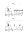
- FIGS. 1 to 17 are sectional views of various steps in the semiconductor device manufacturing process according to the first embodiment.
- the nonvolatile memory cell is, for example, a split-gate cell which uses a MONOS film.
- the low-voltage MIS transistor is, for example, a low-voltage MIS transistor which constitutes a CPU formed in a logical operation circuit module.
- the high-voltage MIS transistor is, for example, a high-voltage MIS transistor which constitutes a power supply circuit for supplying high voltage to the nonvolatile memory module.
- the region in which a nonvolatile memory cell is formed is called memory cell region 1 A
- the region in which a low-voltage MIS transistor is formed is called low-voltage MIS region 1 B
- the region in which a high-voltage MIS transistor is formed is called high-voltage MIS region 1 C.
- FIGS. 1 to 17 the memory cell region 1 A, low-voltage MIS region 1 B, and high-voltage MIS region 1 C are shown from left to right.
- a semiconductor substrate SB of p-type monocrystalline silicon with a resistivity of about 1 ⁇ cm to 10 ⁇ cm is provided as shown in FIG. 1 .
- a semiconductor substrate SB which does not use silicon may be used.
- element isolation areas EI are formed in the main surface of the semiconductor substrate SB.
- element isolation areas EI are formed by making isolation trenches in the semiconductor substrate SB and burying an insulating film such as silicon film in each isolation trench. This element isolation method is called the STI (Shallow Trench Isolation) method.
- the LOCOS Local Oxidization of Silicon
- the thickness of an element isolation area EI is, for example, from 200 nm to 400 nm or so.
- a p-type well PW 1 , p-type well PW 2 , and p-type well PW 3 are formed in the low-voltage MIS region 1 B, high-voltage MIS region 1 C, and memory cell region 1 A of the semiconductor substrate SB, respectively as shown in FIG. 2 .
- the p-type wells PW 1 , PW 2 , and PW 3 are formed by implanting p-type impurity ions (for example, B (boron)).
- a channel region is formed in the main surface of the semiconductor substrate SB in each of the memory cell region 1 A, low-voltage MIS region 1 B, and high-voltage MIS region 1 C, by implanting p-type impurities (for example, B (boron)) using the ion implantation technique, though not shown.
- p-type impurities for example, B (boron)
- an insulating film GI 1 is formed on the main surface (surfaces of the p-type wells PW 1 and PW 3 ) of the semiconductor substrate SB in the low-voltage MIS region 1 B and memory cell region 1 A and an insulating film GI 2 is formed on the main surface (surface of the p-type well PW 2 ) of the semiconductor substrate SB in the high-voltage MIS region 1 C.
- the thickness of the insulating film GI 1 is, for example, 2 nm to 3 nm and the thickness of the insulating film GI 2 is, for example, 10 nm to 15 nm.
- the insulating films GI 1 and GI 2 are, for example, a silicon oxide film made by thermal oxidation, but another type of insulating film such as oxynitride silicon film may be used. Alternatively, a metal oxide film having a higher permittivity than silicon nitride film, such as hafnium oxide film, aluminum oxide film (alumina) or tantalum oxide film, or a laminated film of oxide film and metal oxide film may be formed. Instead of the thermal oxidation technique, the CVD (Chemical Vapor Deposition) technique may be adopted. Alternatively, the insulating film GI 1 and insulating film GI 2 may be different in film type.
- a silicon film SI 1 as a conductive film is formed over the entire surface of the semiconductor substrate SB as shown in FIG. 3 .
- the thickness of the silicon film SI 1 is, for example, 50 nm to 150 nm or so.
- This silicon film SI 1 may be a polycrystalline silicon film made, for example, by the CVD technique.
- the silicon film SI 1 may be formed by depositing an amorphous silicon film and crystallizing it by heat treatment (crystallization).
- the silicon film SI 1 will be used for the gate electrode of a low-voltage MIS transistor in the low-voltage MIS region 1 B, the gate electrode of a high-voltage MIS transistor in the high-voltage MIS region 1 C, and the control gate electrode of a nonvolatile memory cell in the memory cell region 1 A.
- n-type impurities for example, P (phosphorus) or As (arsenic) are implanted into the silicon film SI 1 in the memory cell region 1 A.
- a silicon oxide film (cap insulating film) CP 1 is formed over the silicon film SI 1 by thermally oxidizing the surface of the silicon film SI 1 .
- the thickness of the silicon oxide film CP 1 is, for example, 3 nm to 10 nm or so.
- the silicon oxide film CP 1 may be formed by the CVD technique.
- a silicon nitride film (cap insulating film) CP 2 is formed over the silicon oxide film CP 1 by the CVD technique, etc.
- the thickness of the silicon nitride film CP 2 is, for example, 50 nm to 150 nm or so.
- a photoresist film (not shown) is formed by the photolithographic technique in the portion of the memory cell region 1 A in which the control gate electrode CG is to be formed, the low-voltage MIS region 1 B, and the high-voltage MIS region 1 C, and using the photoresist film as a mask, etching is done on the silicon nitride film CP 2 , silicon oxide film CP 1 , silicon film SI 1 , and insulating film GI 1 in the memory cell region 1 A. After that, the photoresist film is removed by asking, etc. to form the control gate electrode CG based on the silicon film SI 1 (for example, with a gate length of about 80 nm) in the memory cell region 1 A.
- the main surface portion of the semiconductor substrate SB beside the control gate electrode CG is exposed at least from the silicon nitride film CP 2 , silicon oxide film CP 1 and silicon film SI 1 .
- the main surface portion of the semiconductor substrate SB is also exposed from the insulating film GI 1 .
- the insulating film GI 1 remaining under the control gate electrode CG is to become the gate insulating film of the control transistor to be formed later.
- the cap insulating films (silicon nitride film CP 2 and silicon oxide film CP 1 ) lie over the control gate electrode CG, the height of the control gate electrode area (lamination of the control gate electrode CG and cap insulating films) is relatively large. Consequently, a memory gate electrode MG (which will be described later) can be formed into an adequate shape in a highly controllable manner. Specifically, the sidewall of the memory gate MG in the form of a side wall can be virtually perpendicular to the main surface of the semiconductor substrate SB.
- a channel region CH 1 is formed in the main surface of the semiconductor substrate SB in the memory cell region 1 A by implanting n-type impurities (for example, P (phosphorus) or As (arsenic)) using the silicon nitride film CP 2 and silicon film SI 1 as a mask (mask to prevent impurity implantation) by the ion implantation technique.
- n-type impurities for example, P (phosphorus) or As (arsenic)
- a pair of channel regions CH 1 are formed in the main surface of the semiconductor substrate SB on both sides of the control gate electrode CG.
- the regions including the main surface portions of the semiconductor substrate SB just beneath the control gate electrode and memory gate electrode may be also called channel regions.
- an insulating film CSL (C 1 , C 2 , and C 3 ) is formed over the semiconductor substrate SB including the upper surfaces of the silicon nitride film CP 2 and silicon film SI 1 in accordance with the following procedure.
- a silicon oxide film (bottom oxide film) C 1 is formed over the semiconductor substrate SB including the upper surfaces of the silicon nitride film CP 2 and silicon film SI 1 .
- the silicon oxide film C 1 is formed, for example, by the thermal oxidation technique (preferably ISSG (In Situ Steam Generation) oxidation) and its thickness is, for example, about 4 nm.
- the silicon oxide film C 1 may be formed by the CVD technique.
- a silicon nitride film C 2 is formed over the silicon oxide film C 1 .
- the silicon nitride film C 2 is formed, for example, by the CVD technique and its thickness is, for example, about 10 nm.
- the silicon nitride film C 2 is to become the charge accumulation area of the nonvolatile memory cell and the middle layer of the insulating film (ONO film) CSL.
- a silicon oxide film (top oxide film) C 3 is formed over the silicon nitride film C 2 .
- the silicon oxide film C 3 is formed, for example, by the CVD technique and its thickness is, for example, about 5 nm.
- the insulating film CSL as an ONO (Oxide Nitride Oxide) film which includes the silicon oxide film C 1 , silicon nitride film C 2 , and silicon oxide film C 3 , is formed by taking the above steps.
- ONO Oxide Nitride Oxide
- the silicon nitride film C 2 is used as the charge accumulation area (charge accumulation layer, insulating film with a trap level) inside the insulating film CSL.
- another type of insulating film such as silicon oxynitride film, aluminum oxide film, hafnium oxide film or tantalum oxide film may be used. These films are high-permittivity films which have higher permittivity than the silicon nitride film.
- the charge accumulation layer may be formed using an insulating film with silicon nano-dots.
- the insulating film CSL formed in the memory cell region 1 A functions as the gate insulating film of the memory gate electrode to be formed later and has a charge holding (charge accumulation) function. Therefore, it has a laminated structure having at least three layers, in which the potential barrier height of the inner layer (silicon nitride film C 2 ) is smaller than the potential barrier height of the outer layers (silicon oxide films C 1 and C 3 ). The thickness of each layer has an optimum value for each operation type of the nonvolatile memory cell.
- a silicon film SI 2 as a conductive film is formed over the insulating film CSL.
- the thickness of the silicon film SI 2 is, for example, 20 nm to 100 nm or so.
- the silicon film SI 2 may be, for example, a polycrystalline silicon film formed by the CVD technique, etc.
- the silicon film SI 2 may be formed by depositing an amorphous silicon film and crystallizing it by heat treatment (crystallization). Impurities may be implanted into the silicon film SI 2 as necessary.
- the silicon film SI 2 is to become the memory gate electrode (for example, with a gate length of about 50 nm) of the memory cell MC in the memory cell region 1 A as stated later.
- the silicon film SI 2 is etched back.
- the silicon film SI 2 is removed by a prescribed thickness amount from its surface by anisotropic dry etching.
- the silicon film SI 2 remains in the form of side walls (sidewall films) on the sidewall parts on both sides of the control gate electrode CG through the insulating film CSL.
- the silicon film SI 2 is etched and thus the insulating film CSL is exposed.
- the silicon film SI 2 remains as a silicon spacer SP 2 on the sidewall of the silicon film SI 1 through the insulating film CSL, in the form of a side wall (sidewall film).
- a memory gate electrode MG is formed from the silicon film SI 2 remaining on one of both the sidewall parts of the control gate electrode CG.
- a silicon spacer SP 1 is formed from the silicon film SI 2 remaining on the other sidewall part.
- the insulating film CSL under the memory gate electrode MG serves as the gate insulating film of the memory transistor.
- the gate length of the memory gate electrode MG is determined depending on the thickness of the silicon film SI 2 .
- the memory gate electrode MG is formed on the sidewall of the control gate electrode area (film lamination of the control gate electrode CG and cap insulating films) through the insulating film CSL, in the form of a side wall (sidewall film). Therefore, by making the control gate electrode area high enough, the memory gate electrode MG can be formed into an adequate shape in a highly controllable manner. In addition, since the memory gate electrode MG can have an adequate height, the side wall SW on the sidewall of the memory gate electrode MG can be formed into an adequate shape in a highly controllable manner. Furthermore, an extension region EX 2 and a diffusion layer DL 2 to be formed by implanting n-type impurities using the memory gate electrode MG and the side wall SW as a mask can be shaped adequately in a highly controllable manner.
- the insulating film CSL lies between the memory gate electrode MG and the main surface of the semiconductor substrate SB, and the insulating film CSL extends continuously from between the memory gate electrode MG and the main surface of the semiconductor substrate SB along the area between the memory gate electrode MG and the sidewall of the control gate electrode CG.
- the insulating film CSL has an L-shaped sectional structure.
- the silicon spacer SP 1 on the sidewall of the control gate electrode CG where the memory gate electrode MG is not formed, and the silicon spacer SP 2 adjacent to the silicon film SI 1 through the insulating film CSL are removed by etching, as shown in FIG. 7 .
- the insulating film exposed from the memory gate electrode MG is removed by etching. Consequently, the silicon film SI 1 is exposed in the low-voltage MIS region 1 B and high-voltage MIS region 1 C.
- the silicon nitride film CP 2 on the top of the control gate electrode CG is exposed and the p-type well PW 3 with a channel region CH 1 formed in the upper surface is exposed.
- n-type impurities such as P (phosphorous) are implanted into the silicon film SI 1 .
- a photoresist film (not shown) is formed over the silicon film SI 1 by the photolithographic technique in areas where the gate electrodes of a low-voltage MIS transistor and a high-voltage MIS transistor are to be formed, and using the photoresist film as a mask, the silicon film SI 1 and the insulating films GI 1 and GI 2 are etched. Then, the photoresist film is removed by asking, etc. so that a gate electrode GE 1 is formed for the low-voltage MIS transistor in the low-voltage MIS region 1 B and agate electrode GE 2 is formed for the high-voltage MIS transistor in the high-voltage MIS region 1 C.
- the gate length of the gate electrode GE 1 is, for example, about 40 nm and the gate length of the gate electrode GE 2 is, for example, about 1000 nm.
- the insulating film GI 1 remaining under the gate electrode GE 1 serves as the gate insulating film of the low-voltage MIS transistor and the insulating film GI 2 remaining under the gate electrode GE 2 serves as the gate insulating film of the high-voltage MIS transistor.
- a photoresist film (not shown) is formed, in which it has an opening to expose the main surface of the semiconductor substrate SB in an area adjacent to the sidewall of the control gate electrode CG (on the opposite side of the memory gate electrode MG).
- the photoresist film is a resist pattern which covers the main surface portion of the semiconductor substrate SB adjacent to the memory gate electrode MG, the low-voltage MIS region 1 B, and the high-voltage MIS region 1 C.
- p-type impurities are obliquely implanted into the main surface of the semiconductor substrate SB using the photoresist film pattern as a mask.
- a halo region (p-type impurity region) HL 1 is formed in the semiconductor substrate SB under the control gate electrode CG.
- the halo region HL 1 suppresses the spread of a depletion layer from the drain region to be formed later, toward the channel region of the memory transistor and thereby suppresses the short channeling effect of the memory transistor. This suppresses the decrease in the threshold voltage of the memory transistor.
- n-type impurities such as As (arsenic) or P (phosphorous) are implanted into the semiconductor substrate SB to form an extension region EX 1 as an n ⁇ -type semiconductor region.
- the extension region EX 1 is formed in the main surface of the semiconductor substrate SB by self-alignment with the sidewall of the control gate electrode CG (sidewall opposite to the sidewall adjacent to the memory gate electrode MG through the insulating film CSL). After that, the photoresist film is removed.
- a photoresist film (not shown) is formed, in which it has an opening to expose the main surface of the semiconductor substrate SB in an area adjacent to the memory gate electrode MG.
- the photoresist film is a resist pattern which covers the main surface portion of the semiconductor substrate SB adjacent to the control gate electrode CG, the low-voltage MIS region 1 B, and the high-voltage MIS region 1 C.
- n-type impurities such as As (arsenic) or P (phosphorous) are implanted into the upper surface of the semiconductor substrate SB (p-type well PW 3 ) to form an extension region EX 2 as an n ⁇ -type semiconductor region.
- the extension region EX 2 is formed by self-alignment with the sidewall of the memory gate electrode MG (sidewall opposite to the sidewall adjacent to the control gate electrode CG through the insulating film CSL).
- extension region EX 2 In forming the extension region EX 2 , ion implantation is performed with a higher ion concentration than in the ion implantation step of forming the extension region EX 1 . In other words, then-type impurity concentration of the extension region EX 2 is higher than the n-type impurity concentration of the extension region EX 1 .
- the extension region EX 1 and the extension region EX 2 are almost the same in terms of formation depth. It has been mentioned above that the extension regions EX 1 and EX 2 are formed in different steps. However, the extension regions EX 1 and EX 2 may be formed in the same ion implantation step.
- a photoresist film is formed to expose the main surface of the semiconductor substrate SB in the low-voltage MIS region 1 B and cover the memory cell region 1 A and high-voltage MIS region 1 C.
- p-type impurities are obliquely implanted into the main surface of the semiconductor substrate SB. Consequently, a p-type halo region (p-type impurity region) HL 2 is formed in the semiconductor substrate SB beside the gate electrode GE 1 .
- n-type impurities such as As (arsenic) or P (phosphorous) are implanted into the upper surface of the semiconductor substrate SB (p-type well PW 1 ) to form an extension region EX 3 as an n ⁇ -type semiconductor region.
- the extension region EX 3 is formed in the main surface of the semiconductor substrate SB on both sides of the gate electrode GE 1 .
- the extension region EX 3 is formed by self-alignment with the sidewall of the gate electrode GE 1 .
- the extension region EX 3 is shallower in formation depth than the extension regions EX 1 and EX 2 . Since the extension region EX 3 is shallow, the low-voltage MIS transistor including the extension region EX 3 can operate at higher speed.
- the extension region EX 3 is covered by the halo region HL 2 in the semiconductor substrate SB.
- a photoresist film (not shown) is formed to cover the memory cell region 1 A and low-voltage MIS region 1 B and expose the high-voltage MIS region 1 C.
- n-type impurities such as As (arsenic) or P (phosphorous) are implanted into the upper surface of the semiconductor substrate SB (p-type well PW 2 ) to form an extension region EX 4 as an n ⁇ -type semiconductor region.
- the extension region EX 4 is formed in the main surface of the semiconductor substrate SB on both sides of the gate electrode GE 2 .
- the extension region EX 4 is formed by self-alignment with the sidewall of the gate electrode GE 2 .
- the extension region EX 4 has a larger formation depth than any of the extension regions EX 1 to EX 3 . Since the extension region EX 4 has a large depth, it is possible to prevent the possibility that the n-type impurities contained in the extension region EX 4 spread widely during the heat treatment which will be described referring to FIG. 14 and the impurity concentration difference between the n-type semiconductor region of the source/drain region of the high-voltage MIS transistor and the p-type well PW 2 becomes considerable. Therefore, the breakdown voltage of the high-voltage MIS transistor can be increased.
- the halo region HL 2 has a larger formation depth than any of the extension regions EX 1 to EX 4 .
- the extension regions EX 1 , EX 2 , and EX 3 are formed in different ion implantation steps. Since the extension regions EX 1 to EX 3 are thus formed in different ion implantation steps, each of the extension regions EX 1 to EX 3 can be formed with the desired impurity concentration and the desired junction depth. In other words, the concentration distribution of the extension regions and the source/drain regions to be formed later can be set more freely than when two or more types of extension regions among the extension regions EX 1 to EX 3 are formed in an ion implantation step.
- the extension region EX 1 may be formed before the halo region HL 1 is formed. Also, the extension region EX 3 may be formed before the halo region HL 2 is formed. The formation of the halo region HL 1 and extension region EX 1 , the formation of the extension region EX 2 , and the formation of the halo region HL 2 and extension region EX 3 maybe carried out in any sequence.
- the extension region EX 1 is formed inside the halo region HL 1 .
- the halo region HL 1 is deeper than the extension region EX 1 and the end of the extension region EX 1 on the memory gate electrode MG side is covered by the halo region HL 1 .
- Part of the halo region HL 1 overlaps the entire channel region CH 1 on the control gate electrode CG side.
- the extension region EX 1 , halo region HL 1 , p-type well PW 3 , channel region CH 1 , and extension region EX 2 are arranged on the main surface of the semiconductor substrate SB in the order of mention in the direction from the extension region EX 1 to the extension region EX 2 .
- side walls SW as sidewall insulating films are formed on the sidewall parts on both sides of the combination pattern of the control gate electrode CG and memory gate electrode MG.
- side walls SW are formed on the sidewall parts on both sides of each of the gate electrodes GE 1 and GE 2 .
- an insulating film as a laminate including a silicon oxide film and a silicon nitride film is formed, for example, by depositing a silicon oxide film over the entire main surface of the semiconductor substrate SB and depositing a silicon nitride film over it.
- the main surface of the semiconductor substrate SB and the upper surfaces of the control gate electrode CG, memory gate electrode MG, and gate electrodes GE 1 and GE 2 are exposed by etching the insulating film.
- Side walls SW are thus formed on the sidewall parts of the combination pattern, the sidewall parts of the gate electrode GE 1 , and the sidewall parts of the gate electrode GE 2 .
- the side wall SW may be a laminate including a silicon oxide film and a silicon nitride film or may be an insulating film as a single-layer silicon oxide film or a single-layer silicon nitride film.
- a photoresist film PR 1 is formed to cover part of the memory cell region 1 A and entirely cover the main surface of the semiconductor substrate SB in the low-voltage MIS region 1 B and high-voltage MIS region 1 C.
- the photoresist film PR 1 covers the main surface of the semiconductor substrate SB at least in an area adjacent to the memory gate electrode MG.
- the photoresist film PR 1 also covers the upper surface of the memory gate electrode MG.
- the photoresist film PR 1 exposes the main surface of the semiconductor substrate SB in an area adjacent to the control gate electrode CG and exposes the upper surface of the silicon nitride film CP 2 .
- n-type impurities such as As (arsenic) or P (phosphorous) are implanted into the upper surface of the semiconductor substrate SB (p-type well PW 3 ) on the control gate electrode CG side in the memory cell region 1 A.
- a diffusion layer DL 1 as an n + -type semiconductor region with a high impurity concentration is thus formed in the main surface of the semiconductor substrate SB on the control gate electrode CG side in the memory cell region 1 A.
- the diffusion layer DL 1 is formed by self-alignment with the side wall SW on the control gate electrode CG side.
- the n-type impurity concentration of the diffusion layer DL 1 is higher than that of the extension region EX 1 and its junction depth (formation depth) is larger.
- the formation depth of the diffusion layer DL 1 is decreased by using a relatively low level of implantation energy.
- this ion implantation step since the main surface of the semiconductor substrate SB on the memory gate electrode MG side is covered by the photoresist film PR 1 , no diffusion layer is formed in the semiconductor substrate SB on the memory gate electrode MG side.
- a photoresist film PR 2 is formed to cover part of the memory cell region 1 A and entirely cover the main surface of the semiconductor substrate SB in the low-voltage MIS region 1 B and high-voltage MIS region 1 C.
- the photoresist film PR 2 covers the main surface of the semiconductor substrate SB at least in an area adjacent to the control gate electrode CG.
- the photoresist film PR 2 also covers the upper surface of the silicon nitride film CP 2 .
- the photoresist film PR 2 exposes the main surface of the semiconductor substrate SB in an area adjacent to the memory gate electrode MG and exposes the upper surface of the memory gate electrode MG.
- n-type impurities such as As (arsenic) or P (phosphorous) are implanted into the upper surface of the semiconductor substrate SB (p-type well PW 3 ) on the memory gate electrode MG side in the memory cell region 1 A.
- a diffusion layer DL 2 as an n + -type semiconductor region with a high impurity concentration is thus formed in the main surface of the semiconductor substrate SB on the memory gate electrode MG side in the memory cell region 1 A.
- the diffusion layer DL 2 is formed by self-alignment with the side wall SW on the memory gate electrode MG side.
- the n-type impurity concentration of the diffusion layer DL 2 is higher than that of the extension regions EX 1 and EX 2 and its junction depth (formation depth) is larger.
- the formation depth of the diffusion layer DL 2 is made larger than the formation depth of the diffusion layer DL 1 by using a relatively high level of implantation energy.
- n-type impurities are not implanted into it.
- the formation depth of the diffusion layer DL 2 is larger than that of the channel region CH 1 .
- the end of the extension region EX 1 is nearer to the channel region underneath the control gate electrode CG than to the diffusion layer DL 1 and the end of the extension region EX 2 is nearer to the channel region underneath the memory gate electrode MG than to the diffusion layer DL 2 .
- the diffusion layers DL 1 and DL 2 are assumed to have almost the same impurity concentration. However, the diffusion layers DL 1 and DL 2 may have different impurity concentrations. For example, the impurity concentration of the diffusion layer DL 2 may be higher than that of the diffusion layer DL 1 .
- a photoresist film PR 3 is formed to entirely cover the main surface of the semiconductor substrate SB in the memory cell region 1 A and entirely expose the main surface of the semiconductor substrate SB in the low-voltage MIS region 1 B and high-voltage MIS region 1 C.
- n-type impurities such as As (arsenic) or P (phosphorous) are implanted into the upper surface of the semiconductor substrate SB (p-type wells PW 1 , PW 2 ) in the low-voltage MIS region 1 B and high-voltage MIS region 1 C.
- a diffusion layer DL 3 as an n + -type semiconductor region with a high impurity concentration is thus formed in the main surface of the semiconductor substrate SB in the low-voltage MIS region 1 B and high-voltage MIS region 1 C.
- the diffusion layer DL 3 is formed by self-alignment with the side wall SW.
- the n-type impurity concentration of the diffusion layer DL 3 is higher than that of the extension regions EX 3 and EX 4 .
- the formation depth of the diffusion layer DL 3 is larger than that of the extension region EX 3 and smaller than that of the extension region EX 4 and diffusion layer DL 2 .
- the diffusion layers DL 1 , DL 2 , and DL 3 may be formed in any sequence.
- the impurity concentration of the diffusion layer DL 3 is higher than that of the diffusion layers DL 1 and DL 2 . Consequently, the low-voltage MIS transistor to be formed later can operate at higher speed than the control transistor which will be described later, because the resistance of its source/drain region can be decreased.
- the diffusion layer DL 3 has a high impurity concentration, the breakdown voltage of the high-voltage MIS transistor can be increased by diffusion of n-type impurities in the diffusion layer DL 3 . Since the concentration of the diffusion layer DL 1 is lower than that of the diffusion layer DL 3 , the n-type impurities in the diffusion layer DL 1 are prevented from spreading widely in the semiconductor substrate SB. This prevents the decrease in the threshold voltage of the control transistor to be formed later.
- heat treatment is carried out on the semiconductor substrate SB in order to diffuse the impurities implanted into the semiconductor substrate SB and activate the various semiconductor regions. Consequently, the n-type impurities are diffused from the extension region EX 1 and diffusion layer DL 1 in the semiconductor substrate SB, resulting in the formation of a diffusion region DR 1 as an n-type semiconductor region.
- the heat treatment diffuses the n-type impurities from the extension region EX 2 and diffusion layer DL 2 in the semiconductor substrate SB, resulting in the formation of a diffusion region DR 2 as an n-type semiconductor region.
- the heat treatment also diffuses the p-type impurities from the halo region HL 1 in the semiconductor substrate SB, resulting in the formation of a diffusion region HR as a p-type semiconductor region.
- the diffusion region DR 1 has a lower impurity concentration than the diffusion layer DL 1 and extension region EX 1 .
- the diffusion region DR 2 has a lower impurity concentration than the diffusion layer DL 2 and extension region EX 2 .
- the diffusion region HR has a lower impurity concentration than the halo region HL 1 .
- the diffusion region DR 2 is joined to the channel region CH 1 of the memory cell region 1 A so that the diffusion region DR 2 extends to the channel region side underneath the control gate electrode CG in the main surface of the semiconductor substrate SB as shown in FIG. 14 .
- the halo region HL 1 and the diffusion region DR 2 are adjacent to each other and the diffusion region HR and the diffusion region DR 2 abut on each other.
- the diffusion region DR 1 shown in the figure indicates the range of diffusion of the n-type impurities from the diffusion layer DL 1 . Therefore, in some cases, even if the extension region EX 1 overlaps the control gate electrode CG in a plan view, the diffusion region DR 1 does not overlap the control gate electrode CG.
- the end of the extension region EX 1 on the diffusion layer DL 2 side is not covered by the diffusion region DR 1 . Specifically, the end of the extension region EX 1 on the diffusion layer DL 2 side is nearer to the diffusion layer DL 2 than to the diffusion region DR 1 . In other words, in the main surface of the semiconductor substrate SB, the end of the diffusion region DR 1 on the diffusion layer DL 2 side is nearer to the diffusion layer DL 1 than the end of the extension region EX 1 on the diffusion layer DL 2 side.
- the difference in formation depth between the diffusion region DR 2 and the diffusion layer DL 2 is larger than the difference in formation depth between the diffusion region DR 1 and the diffusion layer DL 1 .
- the distance from the bottom of the diffusion layer DL 2 to the bottom of the diffusion region DR 2 is larger than the distance from the bottom of the diffusion layer DL 1 to the bottom of the diffusion region DR 1 and thus the diffusion region DR 2 extends more deeply and more widely than the diffusion region DR 1 .
- the extension region EX 2 is covered by the diffusion region DR 2 and the diffusion layer DL 2 .
- the end of the extension region EX 2 on the diffusion layer DL 1 side is covered by the diffusion region DR 2 .
- the end of the diffusion region DR 2 on the diffusion layer DL 1 side is nearer to the diffusion layer DL 1 than the end of the extension region EX 2 on the diffusion layer DL 1 side.
- the formation depth of the diffusion region (not shown) containing the n-type impurities diffused from the diffusion layer DL 3 is smaller than that of the diffusion region DR 2 .
- the extension region EX 1 , diffusion layer DL 1 , and diffusion region DR 1 constitute an n-type drain region which functions as the drain region of the memory transistor.
- the extension region EX 2 , diffusion layer DL 2 , and diffusion region DR 2 constitute an n-type source region which functions as the source region of the memory transistor.
- the extension region EX 3 and diffusion layer DL 3 constitute a source/drain region.
- Each source region and each drain region have an LDD (Lightly Doped Drain) structure which includes a diffusion layer with a high n-type impurity concentration and an extension region with a low n-type impurity concentration which is adjacent to the diffusion layer in the main surface of the semiconductor substrate SB.
- LDD Lightly Doped Drain
- the source region, drain region, and control gate electrode CG in the memory cell region 1 A constitute a control transistor as an n-channel field effect transistor. Furthermore, the source region, drain region, and memory gate electrode MG in the memory cell region 1 A constitute a memory transistor as an n-channel field effect transistor. This means that the control transistor and the memory transistor share the source and drain regions.
- the control transistor and memory transistor, which are adjacent to each other, constitute a MONOS memory cell MC.
- the control transistor is an enhancement-type transistor and the memory transistor is a depletion-type transistor.
- the source/drain regions and the gate electrode GE 1 in the low-voltage MIS region 1 B constitute a low-voltage MISQ 1 and the source/drain regions and the gate electrode GE 2 constitute a high-voltage MISQ 2 .
- the low-voltage MISQ 1 is a transistor which operates at lower voltage than the high-voltage MISQ 2 and is a semiconductor element which can operate at higher speed than the high-voltage MISQ 2 , control transistor and memory transistor.
- the high-voltage MISQ 2 is a transistor which operates at higher voltage than the control transistor.
- a silicide layer S 1 is formed over each of the memory gate electrode MG, gate electrodes GE 1 and GE 2 , and diffusion layers DL 1 to DL 3 using the salicide (self-aligned silicide) technique.
- the silicide layer S 1 can decrease the diffusion resistance and contact resistance.
- the silicide layer S 1 is formed in accordance with the following procedure.
- a metal film (not shown) is formed over the entire main surface of the semiconductor substrate SB and heat treatment is performed on the semiconductor substrate SB so that the upper layers of the memory gate electrode MG, gate electrodes GE 1 and GE 2 and diffusion layers DL 1 to DL 3 react with the metal film.
- the silicide layer S 1 is thus formed over each of the memory gate electrode MG, gate electrodes GE 1 and GE 2 , and diffusion layers DL 1 to DL 3 .
- the metal film is, for example, a cobalt (Co) or nickel (Ni) film which can be formed by sputtering, etc. After that, the unreacted metal film portion is removed.
- an interlayer insulating film IL is formed over the entire main surface of the semiconductor substrate SB to cover the memory cell MC, low-voltage MISQ 1 transistor, and high-voltage MISQ 2 transistor.
- the interlayer insulating film IL is a single silicon oxide film or a laminated film including a silicon nitride film and a silicon oxide film. After the interlayer insulating film IL is formed, for example, by the CVD technique, the upper surface of the interlayer insulating film is planarized.
- plugs PG which penetrate the interlayer insulating film IL are formed as follows. First, a photoresist film (not shown) is formed by the photolithographic technique, and using the photoresist film as a mask, the interlayer insulating film IL is etched to make a plurality of contact holes in the interlayer insulating film IL. Then, a conductive plug PG of tungsten (W), etc. is formed in each contact hole.
- W tungsten
- plugs PG In order to form plugs PG, a barrier conductor film such as a titanium (Ti) film, titanium nitride (TiN) film or a laminated film of these is formed over the interlayer insulating film IL including the inside of each of the contact holes. Then, a main conductor film such as a tungsten (W) film is formed over the barrier conductor film so as to fill each contact hole and the unrequired portions of the main conductor film and barrier conductor film are removed by the CMP (Chemical Mechanical Polishing) technique or etch-back technique. The plugs PG are thus formed. For illustration simplicity, the barrier conductor film and main conductor film which constitute the plugs PG are shown in an integrated form.
- CMP Chemical Mechanical Polishing
- the contact holes and the plugs PG buried in them are coupled to the upper surfaces of the diffusion layers DL 1 to DL 3 through the silicide layers S 1 .
- the plugs PG are coupled to the upper surfaces of the control gate electrode CG, memory gate electrode MG, and gate electrodes GE 1 and GE 2 through the silicide layers S 1 .
- an interlayer insulating film IL 1 such as a silicon oxide film is formed over the interlayer insulating film IL
- a plurality of wiring grooves which penetrate the interlayer insulating film IL 1 are formed by the photolithographic technique and dry etching technique.
- a conductive film is deposited and buried in each wiring groove and the conductive film lying over the interlayer insulating film IL 1 is removed. Consequently, a plurality of wirings M 1 which are made of the conductive film and electrically coupled to the plugs PG are formed.
- the wirings M 1 are mainly made of copper (Cu).
- the semiconductor device according to this embodiment is almost finished. Specifically, a low-voltage MISQ 1 transistor, a high-voltage MISQ 2 transistor, and a memory cell MC as a nonvolatile memory cell are formed in the low-voltage MIS region 1 B, high-voltage MIS region 1 C, and memory cell region A, respectively.
- the operation of the memory cell MC as a nonvolatile memory cell includes writing, erasing, and reading.
- the SSI (Source Side Injection) method is adopted for writing and erasing.
- injection of electrons into the silicon nitride film C 2 as a charge accumulation area in the insulating film CSL as an ONO film is defined as “writing” and extraction of electrons from it is defined as “erasing”.
- a plurality of memory cells MC are arranged in an array pattern over the semiconductor substrate SB and writing, erasing, and reading operations are performed only on the desired memory cells MC among these memory cells MC. This means that writing, erasing, and reading operations are usually not performed on the non-selected memory cells or cells other than the selected memory cells.
- a non-selected memory cell arranged in the same row as a selected memory cell is coupled to the same memory gate line as the selected memory cell. Also, in the memory cell array, a non-selected memory cell arranged in the same column as a selected memory cell is coupled to the same word line (control gate line) as the selected memory cell. This means that the same voltage is applied to the memory gate electrodes MG of the memory cells arranged in the same row and the same voltage is applied to the control gate electrodes CG of the memory cells arranged in the same column.
- the following voltages are applied to the various parts of a memory cell MC to operate for writing, namely a selected memory cell.
- 0 V is applied to the semiconductor substrate SB
- 6 V is applied to the source region including the diffusion layer DL 2
- 0.5 V is applied to the drain region including the diffusion layer DL 1
- 1 V is applied to the control gate electrode CG
- 12 V is applied to the memory gate electrode MG. Consequently, electrons move from the drain region to the source region.
- the electrons are trapped at the trap level in the silicon nitride film C 2 and as a consequence, the threshold voltage of the transistor of the memory cell MC rises. That is, the memory cell MC enters the writing state.
- the voltage applied to the drain region is higher than in the selected memory cell, so that a current does not flow between the source and drain regions. For this reason, writing is not performed.
- the erasing method in which erasing is performed by injection of hot holes according to the so-called BTBT (Band-To-Band Tunneling) method (hot hole injection erase) is adopted.
- BTBT Band-To-Band Tunneling
- erasing is performed by injecting the holes (positive holes) generated by BTBT into the charge accumulation area (silicon nitride film C 2 ).
- the following voltages are applied to the various parts of the selected memory cell to operate for erasing.
- 0 V is applied to the semiconductor substrate SB
- 6 V is applied to the source region including the diffusion layer DL 2
- 1.5 V is applied to the drain region including the diffusion layer DL 1
- 0 V is applied to the control gate electrode CG
- ⁇ 6 V is applied to the memory gate electrode MG.
- the voltage applied to the control gate electrode CG is between the transistor threshold voltage in the writing state and its threshold voltage in the erased state so that the writing state and the erased state can be distinguished from each other.
- 0 V is applied to the semiconductor substrate SB, the memory gate electrode MG, and the source region and 1.5 V is applied to the drain region and the control gate electrode CG.
- the threshold voltage is high and thus the transistor does not turn on.
- the threshold voltage is low and thus the transistor turns on. Since the transistor operates differently in this way, data can be read from the memory cell MC.
- FIG. 30 is a sectional view of a step in the semiconductor device manufacturing process in Comparative Example 2 in which the control gate electrode gate length is relatively large and FIGS. 28 and 29 are sectional views of steps in the semiconductor device manufacturing process in Comparative Example 1 in which the control gate electrode gate length is smaller than in the structure shown in FIG. 30 .
- FIGS. 28 to 30 show the memory cell region 1 A, low-voltage MIS region 1 B, and high-voltage MIS region 1 C in the same way as FIGS. 1 to 17 .
- the p-type impurity concentration of the halo region HL 1 formed here is higher than that of the halo region HL 1 (see FIG. 9 ) formed in the semiconductor device manufacturing process according to the first embodiment.
- a photoresist film PR is formed to cover the main surface of the semiconductor substrate SB in the low-voltage MIS region 1 B and high-voltage MIS region 1 C and expose the memory cell region 1 A.
- n-type impurity ions such as P (phosphorous) or As (arsenic) are implanted into the main surface of the semiconductor substrate SB to form diffusion layers DLD and DLS which have a higher impurity concentration than the extension regions EX 1 to EX 4 .
- the diffusion layer DLD is formed in the main surface of the semiconductor substrate SB on the control gate electrode CG side and the diffusion layer DLS is formed in the main surface of the semiconductor substrate SB on the memory gate electrode MG side.
- the diffusion layers DLD and DLS are n-type semiconductor regions which are larger in formation depth than the extension regions EX 1 to EX 4 and smaller in formation depth than the halo region HL 1 . Since the diffusion layers DLD and DLS are formed in the same implantation step as mentioned above, they have virtually the same formation depth.
- the formation depth of the diffusion layers DLD and DLS is, for example, the same as that of the diffusion layer DL 2 shown in FIG. 17 .
- a diffusion layer DL 3 (see FIG. 29 ) is formed in each of the low-voltage MIS region 1 B and high-voltage MIS region 1 C by taking the same step as the step described above referring to FIG. 13 .
- the impurities in the semiconductor substrate SB are diffused and heat treatment is performed to activate the semiconductor regions in the semiconductor substrate SB. Consequently, the n-type impurities contained in the diffusion layers DLD and DLS diffuse into the semiconductor substrate SB so that a diffusion region DRD containing the n-type impurities spread around the diffusion layer DLD and a diffusion region DRS containing the n-type impurities spread around the diffusion layer DLS are formed.
- the diffusion region DRS has the same structure as the diffusion region DR 2 shown in FIG. 14 .
- the diffusion region DRD has the same formation depth as the diffusion region DRS and covers the end of the extension region EX 1 on the extension region EX 2 side.
- a drain region including the diffusion region DRD, diffusion layer DLD, and extension region EX 1 and a source region including the diffusion region DRS, diffusion layer DLS, and extension region EX 2 are formed and a memory cell MC 1 , which includes the drain region, the source region and a control gate electrode CG and a memory gate electrode MG, is formed.
- the memory cell in Comparative Example 1 is different from that in the first embodiment in that the diffusion layer DLD of the drain region has the same depth as the diffusion layer DLS of the source region and the diffusion region DRD has the same depth as the diffusion region DRS.
- FIG. 30 is a sectional view of a manufacturing step after the heat treatment step described above referring to FIG. 29 .
- the semiconductor device manufacturing process in Comparative Example 2 is almost the same as the above semiconductor device manufacturing process in Comparative Example 1.
- the diffusion layers DLD and DLS are formed simultaneously in the same injection step.
- the gate length of the control gate electrode CG of the memory cell MC 2 is larger than that of the memory cell MC 1 (see FIG. 29 ) in Comparative Example 1.
- the p-type impurity concentrations of the halo region HL 1 and the diffusion region HR are lower than those in the memory cell MC 1 (see FIG. 29 ) in Comparative Example 1.
- the threshold voltage (Vth) of the transistor of the memory cell decreases and it is difficult to control the memory cell.
- the formation of a halo region with the conductivity type opposite to the conductivity type of the drain region between the drain region and channel region prevents worsening of the short channel characteristics and the decrease in the threshold voltage of the transistor.
- the gate length of the control gate electrode CG is large, even if a portion of the diffusion region HR abuts on the source region, the p-type impurity concentration of the diffusion region HR's portion abutting on the source region is low. This means that the difference in n-type impurity concentration between the halo region HL 1 and diffusion region HR and the source region cannot be serious and generation of junction leakage current is thus prevented.
- the n-type impurities of the source region must be gradually diffused around the source region in order to improve the breakdown voltage of the source region. This prevents the impurity concentration difference between the p-type well PW 3 as a p-type semiconductor region and the source region as an n-type semiconductor region from becoming serious, so that the depletion layer easily spreads from the source region and the breakdown voltage of the memory cell MC 1 is improved.
- One method of diffusing the n-type impurities of the source region gradually between the source region and the p-type well region PW 3 is to make the diffusion layer DLS of the source region have a large depth.
- Comparative Example 1 by forming the diffusion layer DLS with a larger depth than the diffusion layer DL 3 in the low-voltage MIS region 1 B or high-voltage MIS region 1 C (see FIG. 29 ), the n-type impurities in the diffusion layer DLS are diffused widely and gradually by heat treatment to form the diffusion region DRS.
- the source region extends so as to partially overlap the memory gate electrode MG in a plan view.
- Comparative Example 1 since the source region and drain region are formed with the same depth and the same concentration in the same step, the n-type impurities of the drain region also diffuse widely in the same way. Consequently, the diffusion region DRD of the drain region largely overlaps the channel region underneath the control gate electrode CG. In this case, since the drain region extends widely and the distance between the source and drain regions is short, the effective gate length and channel length are short. This worsens the short channel characteristics and decreases the threshold voltage of the control transistor.
- One possible method of increasing the threshold voltage of the control transistor is to increase the concentration of the halo region HL 1 as a p-type semiconductor region which covers the drain region and spreads toward the source region side in the semiconductor substrate SB or increase the p-type impurity concentration of the channel region.
- the concentration difference in the PN junction between the halo region HL 1 and the source region is larger, thereby increasing the risk of miswriting in a non-selected memory cell in writing operation of the memory cell MC.
- the concentration difference in the PN junction between the halo region HL 1 and the source region is larger, carriers are generated in the PN junction near the border between the control gate electrode CG and the memory gate electrode MG and a junction leakage current flows in the source region.
- Some of the carriers generated here are, as hot carriers, drawn toward the high voltage of the memory gate electrode MG and passed through the silicon oxide film (bottom oxide film) C 1 of the insulating film CSL as an ONO film and introduced into the silicon nitride film (charge accumulation layer) C 2 of the ONO film. Miswriting in a non-selected memory cell occurs in this way.
- control transistor of the memory cell MC 1 is required to operate at high speed, but when the drain region has a large formation depth like the source region as in Comparative Example 1 and Comparative Example 2, it is difficult that the control transistor operates at high speed.
- the diffusion layer DL 1 of the drain region of the memory cell MC (see FIG. 14 ) and the diffusion layer DL 2 of its source region are formed under different conditions in different ion implantation steps, as described above referring to FIGS. 11 and 12 . Therefore, it is possible to form the diffusion layer DL 2 with a large depth and form the diffusion layer DL 1 with a smaller depth than the diffusion layer DL 2 .
- the n-type impurity concentration of the diffusion region DR 2 formed by heat treatment as shown in FIG. 14 gradually decreases in the direction from the diffusion layer DL 2 to the p-type well PW 3 . This prevents the concentration difference between p-type impurities and n-type impurities in the PN junction between the channel region and p-type well PW 3 and the source region from becoming seriously large, thereby increasing the breakdown voltage of the source region.
- the concentration difference between p-type impurities and n-type impurities in the PN junction between the channel region and p-type well PW 3 and the drain region is larger than the concentration difference in the PN junction between the source region and p-type well.
- the voltage applied to the drain region is not so high as the voltage applied to the source region and the problem of decrease in breakdown voltage does not occur.
- the formation depths of the diffusion layer DL 1 and diffusion region DR 1 can be decreased so that high speed operation of the control transistor is easy.
- the diffusion region DR 1 prevents part of the drain region from largely overlapping the control gate electrode CG in a plan view.
- the diffusion region DR 1 does not overlap the control gate electrode CG in a plan view.
- the diffusion layer DL 1 and diffusion region DR 1 are spaced from the control gate electrode CG in a plan view. This ensures that the width of the channel region between the drain region and source region is sufficient, thereby preventing the effective gate length from becoming small. Therefore, even if the gate length of the control gate electrode CG is decreased for miniaturization of the semiconductor element, worsening of the short channel characteristics is prevented.
- the p-type impurity concentrations of the halo region HL 1 and diffusion region HR need not be increased excessively. Therefore, the concentration and formation depth of the halo region HL 1 can be suppressed. Therefore, the p-type impurity concentrations of the halo region HL 1 and diffusion region HR in the vicinity of the source region can be decreased. This prevents the concentration difference in the PN junction between the halo region HL 1 and diffusion region HR and the source region from increasing and also prevents the concentration difference from becoming seriously large.
- the diffusion layer DL 1 of the drain region and the diffusion layer DL 2 of the source region are formed in different steps and the source/drain region is asymmetrical in shape. This prevents miswriting in the memory cell and makes it possible to miniaturize the memory cell MC and increase its breakdown voltage and enables high speed operation, thereby leading to improvement in the performance of the semiconductor device.
- FIGS. 18 and 19 are sectional views of steps in the semiconductor device manufacturing process as a variation of the first embodiment.
- This variation is the same as the first embodiment described above referring to FIGS. 1 to 17 in that the diffusion layers of the source and drain regions of the memory cell are formed in different steps.
- This variation is different from the process described above referring to FIGS. 1 to 17 in that the diffusion layers of the source and drain regions are the same in depth and different in concentration.
- n-type impurities are implanted into the main surface of the semiconductor substrate SB on the control gate electrode CG side with a relatively low concentration to form a diffusion layer DL 1 , as shown in FIG. 18 .
- the impurity concentration of the diffusion layer DL 1 is lower than that of the diffusion layer DL 1 described referring to FIG. 11 and the diffusion layer DLD described referring to FIG. 28 .
- ion implantation is performed with a relatively high impurity concentration to form a diffusion layer DL 2 (see FIG. 19 ).
- the ion implantation steps of forming the diffusion layers DL 1 and DL 2 are carried out under almost the same energy condition, so that the diffusion layers DL 1 and DL 2 have almost the same formation depth.
- the diffusion layer DL 2 has a higher n-type impurity concentration than the diffusion layer DL 1 .
- the impurity concentration of the diffusion layer DL 2 is lower than that of the diffusion layer DL 2 described referring to FIG. 12 .
- a diffusion layer DL 3 is formed in the low-voltage MIS region 1 B and the high-voltage MIS region 1 C.
- the n-type impurities in the diffusion layers DL 1 to DL 3 are diffused by performing heat treatment as in the step described referring to FIG. 14 . Consequently, a diffusion region DR 1 is formed around the diffusion layer DL 1 and a diffusion region DR 2 is formed around the diffusion layer DL 2 .
- the formation depth of the diffusion region DR 1 is smaller than the formation depth of the diffusion region DR 2 .
- the extent of spread of the diffusion region DR 1 is smaller than that of the diffusion region DR 2 . This is because the impurity concentration of the diffusion layer DL 1 is lower than that of the diffusion layer DL 2 .
- the semiconductor device in this variation is almost finished by taking the same steps as the steps described referring to FIGS. 15 to 17 .
- the spread of the diffusion region DR 1 is suppressed by decreasing the impurity concentration of the diffusion layer DL 1 .
- the difference in formation depth between the diffusion region DR 2 and the diffusion layer DL 2 is larger than the difference in formation depth between the diffusion region DR 1 and the diffusion layer DL 1 .
- the distance from the bottom of the diffusion layer DL 2 to the bottom of the diffusion region DR 2 is larger than the distance from the bottom of the diffusion layer DL 1 to the bottom of the diffusion region DR 1 .
- the diffusion layer DL 1 may have a lower concentration and a smaller formation depth and the diffusion layer DL 2 may have a higher concentration and a larger formation depth.
- FIGS. 20 to 22 are sectional views of steps in the semiconductor device manufacturing process according to the second embodiment.
- a memory cell region 1 A, low-voltage MIS region 1 B, and high-voltage MIS region 1 C are shown as in FIGS. 1 to 17 .
- a photoresist film PR 4 is formed to partially cover the memory cell region 1 A and entirely expose the main surface of the semiconductor substrate SB in the low-voltage MIS region 1 B and the high-voltage MIS region 1 C.
- the photoresist film PR 4 covers the main surface of the semiconductor substrate SB at least in an area adjacent to the memory gate electrode MG.
- the photoresist film PR 4 also covers the upper surface of the memory gate electrode MG.
- the photoresist film PR 4 also exposes the main surface of the semiconductor substrate SB in an area adjacent to the control gate electrode CG and exposes the upper surface of the silicon nitride film CP 2 .
- n-type impurities such as As (arsenic) or P (phosphorous) are implanted into the upper surface of the semiconductor substrate SB.
- a diffusion layer DL 1 is thus formed in the main surface of the semiconductor substrate SB on the control gate electrode CG side in the memory cell region 1 A, a pair of diffusion layers DL 3 are formed in the main surface of the semiconductor substrate SB beside the gate electrode GE 1 and a pair of diffusion layers DL 3 are formed in the main surface of the semiconductor substrate SB beside the gate electrode GE 2 .
- a diffusion layer DL 2 is formed in the main surface of the semiconductor substrate SB on the memory gate electrode MG side in the memory cell region 1 A by taking the same step as the step described referring to FIG. 12 .
- diffusion regions DR 1 , DR 2 , and HR are formed by taking the same step as the step described referring to FIG. 14 .
- a memory cell MC, low-voltage MISQ 1 transistor and high-voltage MISQ 2 transistor are thus formed.
- the subsequent steps are the same as the steps described above referring to FIGS. 15 to 17 and the semiconductor device according to the second embodiment is almost finished by taking those steps.
- the semiconductor device in the second embodiment is structurally the same as in the first embodiment except that the diffusion layers DL 1 and DL 3 are almost the same in terms of concentration and depth.
- the diffusion layers DL 1 and DL 3 are formed in the same ion implantation step under the same implantation condition, they are almost the same in terms of n-type impurity concentration and formation depth.
- the semiconductor device manufacturing cost can be reduced by forming the diffusion layer DL 1 in the memory cell region 1 A, and the diffusion layers DL 3 in the low-voltage MIS region 1 B and high-voltage MIS region 1 C in the same step. This means that the number of steps is smaller than in the process in Comparative Example 1 described above referring to FIGS. 18 and 19 and at the same time the second embodiment brings about the same advantageous effects as the first embodiment.
- FIGS. 23 to 27 are sectional views of steps in the semiconductor device manufacturing process according to the third embodiment.
- a memory cell region 1 A, low-voltage MIS region 1 B, and high-voltage MIS region 1 C are shown as in FIGS. 1 to 17 .
- a silicon nitride film NL and a silicon oxide film OX are sequentially formed (deposited) over the entire main surface of the semiconductor substrate SB, for example, by the CVD technique.
- silicon oxide film OX are removed by etching back to expose the upper surface of the silicon nitride film NL as shown in FIG. 24 .
- Other portions of the silicon oxide film OX remain on the sidewalls of the control gate electrode CG, memory gate electrode MG, gate electrodes GE 1 and GE 2 through the silicon nitride film NL, taking the form of side walls.
- the photoresist film PR 5 is a resist pattern which covers the silicon oxide film OX adjacent to one sidewall of the memory gate electrode MG and both the sidewalls of the gate electrode GE 2 through the silicon nitride film NL.
- the photoresist film PR 5 exposes the silicon oxide film OX adjacent to one sidewall of the control gate electrode CG and both the sidewalls of the gate electrode GE 2 through the silicon nitride film NL.
- the silicon oxide film OX adjacent to one sidewall of the control gate electrode CG and both the sidewalls of the gate electrode GE 1 through the silicon nitride film NL is removed by etching.
- etching back is performed on the silicon nitride film NL using the silicon oxide film OX as a mask.
- the upper surfaces of the semiconductor substrate SB, silicon nitride film CP 2 , and gate electrodes GE 1 and GE 2 are exposed by the etch-back step.
- side walls SW 1 of silicon nitride film NL are formed to cover one sidewall of the control gate electrode CG and both the sidewalls of the gate electrode GE 1 .
- side walls SW 2 of silicon nitride film NL and silicon oxide film OX are formed to cover one sidewall of the memory gate electrode MG and both the sidewalls of the gate electrode GE 2 .
- the width of the side wall SW 2 in the gate length direction of the control gate electrode CG is the sum of the thicknesses of the silicon nitride film NL and silicon oxide film OX; on the other hand, the width of the side wall SW 1 in the same direction is equal to the thickness of the silicon nitride film NL. In short, the width of the side wall SW 2 is larger than the width of the side wall SW 1 .
- “width” means a prescribed film length in the direction along the main surface of the semiconductor substrate SB.
- diffusion layers DL 1 to DL 3 are formed in various ion implantation steps and then diffusion regions DR 1 , DR 2 and HR are formed by heat treatment.
- the subsequent steps are the same as the steps described above referring to FIGS. 15 to 17 and the semiconductor device according to the third embodiment is almost finished by taking those steps.
- the diffusion layers DL 1 and DL 2 have different depths so that the same advantageous effects as in the first embodiment can be achieved. Specifically, the depth of the diffusion layer DL 1 of the drain region is small enough to prevent expansion of the extension region DR and thereby prevent the decrease in the channel length. In this embodiment, since the side walls SW 1 with a relatively small width are used for ion implantation, the diffusion layer DL 1 is nearer to the control gate electrode CG than in the first embodiment, but the above effects prevent worsening of the short channel characteristics.
- the memory cell can be miniaturized and the performance of the semiconductor device is enhanced.
- the diffusion layer DL 2 is remoter from the memory gate electrode MG than in the first embodiment. This prevents breakdown when a high voltage is applied to the source region. Therefore, the performance of the semiconductor device is enhanced.
Applications Claiming Priority (2)
| Application Number | Priority Date | Filing Date | Title |
|---|---|---|---|
| JP2016095047A JP6652445B2 (ja) | 2016-05-11 | 2016-05-11 | 半導体装置の製造方法 |
| JP2016-095047 | 2016-05-11 |
Publications (2)
| Publication Number | Publication Date |
|---|---|
| US20170330891A1 US20170330891A1 (en) | 2017-11-16 |
| US10312252B2 true US10312252B2 (en) | 2019-06-04 |
Family
ID=60297544
Family Applications (1)
| Application Number | Title | Priority Date | Filing Date |
|---|---|---|---|
| US15/486,741 Active 2037-04-29 US10312252B2 (en) | 2016-05-11 | 2017-04-13 | Method of manufacturing semiconductor device |
Country Status (4)
| Country | Link |
|---|---|
| US (1) | US10312252B2 (zh) |
| JP (1) | JP6652445B2 (zh) |
| CN (1) | CN107452747B (zh) |
| TW (1) | TWI731066B (zh) |
Families Citing this family (7)
| Publication number | Priority date | Publication date | Assignee | Title |
|---|---|---|---|---|
| JP2018125518A (ja) * | 2017-02-03 | 2018-08-09 | ソニーセミコンダクタソリューションズ株式会社 | トランジスタ、製造方法 |
| US10242996B2 (en) * | 2017-07-19 | 2019-03-26 | Cypress Semiconductor Corporation | Method of forming high-voltage transistor with thin gate poly |
| US10504912B2 (en) * | 2017-07-28 | 2019-12-10 | Taiwan Semiconductor Manufacturing Co., Ltd. | Seal method to integrate non-volatile memory (NVM) into logic or bipolar CMOS DMOS (BCD) technology |
| CN112470279A (zh) * | 2018-07-30 | 2021-03-09 | 索尼半导体解决方案公司 | 固态摄像装置和电子设备 |
| CN109817632B (zh) * | 2019-01-28 | 2021-01-22 | 上海华虹宏力半导体制造有限公司 | 一种分栅sonos存储器件 |
| WO2022168220A1 (ja) * | 2021-02-04 | 2022-08-11 | ユニサンティス エレクトロニクス シンガポール プライベート リミテッド | 半導体素子を用いたメモリ装置 |
| CN116631472B (zh) * | 2023-07-18 | 2023-10-20 | 全芯智造技术有限公司 | 半导体器件及其制造方法和参数优化方法 |
Citations (5)
| Publication number | Priority date | Publication date | Assignee | Title |
|---|---|---|---|---|
| JPH11144483A (ja) | 1997-11-04 | 1999-05-28 | Oko Denshi Kofun Yugenkoshi | 不揮発性半導体メモリデバイス |
| US20080150023A1 (en) | 2006-12-20 | 2008-06-26 | Elpida Memory, Inc. | Semiconductor memory and manufacturing method thereof |
| US20120132978A1 (en) * | 2010-11-25 | 2012-05-31 | Renesas Electronics Corporation | Semiconductor device and manufacturing method of semiconductor device |
| US20150035034A1 (en) * | 2013-07-30 | 2015-02-05 | Brian A. Winstead | Split gate non-volatile memory cell |
| US20170125252A1 (en) * | 2015-11-02 | 2017-05-04 | Texas Instruments Incorporated | Split-gate lateral extended drain mos transistor structure and process |
Family Cites Families (7)
| Publication number | Priority date | Publication date | Assignee | Title |
|---|---|---|---|---|
| US5912843A (en) * | 1996-03-18 | 1999-06-15 | Integrated Memory Technologies, Inc. | Scalable flash EEPROM memory cell, method of manufacturing and operation thereof |
| JP4675813B2 (ja) * | 2006-03-31 | 2011-04-27 | Okiセミコンダクタ株式会社 | 半導体記憶装置およびその製造方法 |
| JP5205011B2 (ja) * | 2007-08-24 | 2013-06-05 | ルネサスエレクトロニクス株式会社 | 不揮発性半導体装置およびその製造方法 |
| JP2010067645A (ja) * | 2008-09-08 | 2010-03-25 | Renesas Technology Corp | 半導体装置およびその製造方法 |
| US8717389B2 (en) * | 2010-08-06 | 2014-05-06 | Canon Kabushiki Kaisha | Projector array for multiple images |
| JP2016051740A (ja) * | 2014-08-28 | 2016-04-11 | ルネサスエレクトロニクス株式会社 | 半導体装置の製造方法 |
| JP6407651B2 (ja) * | 2014-10-01 | 2018-10-17 | ルネサスエレクトロニクス株式会社 | 半導体装置の製造方法 |
-
2016
- 2016-05-11 JP JP2016095047A patent/JP6652445B2/ja active Active
-
2017
- 2017-04-13 US US15/486,741 patent/US10312252B2/en active Active
- 2017-04-24 TW TW106113544A patent/TWI731066B/zh active
- 2017-05-10 CN CN201710326848.7A patent/CN107452747B/zh active Active
Patent Citations (6)
| Publication number | Priority date | Publication date | Assignee | Title |
|---|---|---|---|---|
| JPH11144483A (ja) | 1997-11-04 | 1999-05-28 | Oko Denshi Kofun Yugenkoshi | 不揮発性半導体メモリデバイス |
| US20080150023A1 (en) | 2006-12-20 | 2008-06-26 | Elpida Memory, Inc. | Semiconductor memory and manufacturing method thereof |
| JP2008153567A (ja) | 2006-12-20 | 2008-07-03 | Elpida Memory Inc | 半導体メモリ及びその製造方法 |
| US20120132978A1 (en) * | 2010-11-25 | 2012-05-31 | Renesas Electronics Corporation | Semiconductor device and manufacturing method of semiconductor device |
| US20150035034A1 (en) * | 2013-07-30 | 2015-02-05 | Brian A. Winstead | Split gate non-volatile memory cell |
| US20170125252A1 (en) * | 2015-11-02 | 2017-05-04 | Texas Instruments Incorporated | Split-gate lateral extended drain mos transistor structure and process |
Also Published As
| Publication number | Publication date |
|---|---|
| US20170330891A1 (en) | 2017-11-16 |
| JP6652445B2 (ja) | 2020-02-26 |
| TW201740490A (zh) | 2017-11-16 |
| CN107452747A (zh) | 2017-12-08 |
| TWI731066B (zh) | 2021-06-21 |
| JP2017204548A (ja) | 2017-11-16 |
| CN107452747B (zh) | 2023-11-07 |
Similar Documents
| Publication | Publication Date | Title |
|---|---|---|
| US10312252B2 (en) | Method of manufacturing semiconductor device | |
| US10411139B2 (en) | Semiconductor device and method of manufacturing the semiconductor device | |
| US6835987B2 (en) | Non-volatile semiconductor memory device in which selection gate transistors and memory cells have different structures | |
| US9379127B2 (en) | Semiconductor device and manufacturing method of semiconductor device | |
| US6900086B2 (en) | Semiconductor device having MISFETs | |
| US9093319B2 (en) | Semiconductor device and manufacturing method thereof | |
| US10446569B2 (en) | Semiconductor device and manufacturing method thereof | |
| US10325899B2 (en) | Semiconductor device including transistors formed in regions of semiconductor substrate and operation method of the same | |
| JP2015026870A (ja) | 半導体装置および半導体装置の製造方法 | |
| JP2011210777A (ja) | 半導体装置およびその製造方法 | |
| JP2005019548A (ja) | 半導体装置およびその製造方法 | |
| JP2004253474A (ja) | 不揮発性半導体記憶装置及びその製造方法 | |
| JP2014103345A (ja) | 半導体装置および半導体装置の製造方法 |
Legal Events
| Date | Code | Title | Description |
|---|---|---|---|
| AS | Assignment |
Owner name: RENESAS ELECTRONICS CORPORATION, JAPAN Free format text: ASSIGNMENT OF ASSIGNORS INTEREST;ASSIGNOR:KAWASHIMA, YOSHIYUKI;REEL/FRAME:042001/0022 Effective date: 20170222 |
|
| STPP | Information on status: patent application and granting procedure in general |
Free format text: NOTICE OF ALLOWANCE MAILED -- APPLICATION RECEIVED IN OFFICE OF PUBLICATIONS |
|
| STPP | Information on status: patent application and granting procedure in general |
Free format text: PUBLICATIONS -- ISSUE FEE PAYMENT RECEIVED |
|
| STPP | Information on status: patent application and granting procedure in general |
Free format text: PUBLICATIONS -- ISSUE FEE PAYMENT VERIFIED |
|
| STCF | Information on status: patent grant |
Free format text: PATENTED CASE |
|
| MAFP | Maintenance fee payment |
Free format text: PAYMENT OF MAINTENANCE FEE, 4TH YEAR, LARGE ENTITY (ORIGINAL EVENT CODE: M1551); ENTITY STATUS OF PATENT OWNER: LARGE ENTITY Year of fee payment: 4 |