US10242836B2 - Devices having an electron emitting structure - Google Patents
Devices having an electron emitting structure Download PDFInfo
- Publication number
- US10242836B2 US10242836B2 US14/385,503 US201314385503A US10242836B2 US 10242836 B2 US10242836 B2 US 10242836B2 US 201314385503 A US201314385503 A US 201314385503A US 10242836 B2 US10242836 B2 US 10242836B2
- Authority
- US
- United States
- Prior art keywords
- electron
- construct
- ray emitting
- ray
- active
- Prior art date
- Legal status (The legal status is an assumption and is not a legal conclusion. Google has not performed a legal analysis and makes no representation as to the accuracy of the status listed.)
- Active, expires
Links
Images


Classifications
-
- H—ELECTRICITY
- H01—ELECTRIC ELEMENTS
- H01J—ELECTRIC DISCHARGE TUBES OR DISCHARGE LAMPS
- H01J3/00—Details of electron-optical or ion-optical arrangements or of ion traps common to two or more basic types of discharge tubes or lamps
- H01J3/14—Arrangements for focusing or reflecting ray or beam
-
- G—PHYSICS
- G01—MEASURING; TESTING
- G01N—INVESTIGATING OR ANALYSING MATERIALS BY DETERMINING THEIR CHEMICAL OR PHYSICAL PROPERTIES
- G01N23/00—Investigating or analysing materials by the use of wave or particle radiation, e.g. X-rays or neutrons, not covered by groups G01N3/00 – G01N17/00, G01N21/00 or G01N22/00
- G01N23/02—Investigating or analysing materials by the use of wave or particle radiation, e.g. X-rays or neutrons, not covered by groups G01N3/00 – G01N17/00, G01N21/00 or G01N22/00 by transmitting the radiation through the material
- G01N23/04—Investigating or analysing materials by the use of wave or particle radiation, e.g. X-rays or neutrons, not covered by groups G01N3/00 – G01N17/00, G01N21/00 or G01N22/00 by transmitting the radiation through the material and forming images of the material
- G01N23/046—Investigating or analysing materials by the use of wave or particle radiation, e.g. X-rays or neutrons, not covered by groups G01N3/00 – G01N17/00, G01N21/00 or G01N22/00 by transmitting the radiation through the material and forming images of the material using tomography, e.g. computed tomography [CT]
-
- G—PHYSICS
- G01—MEASURING; TESTING
- G01T—MEASUREMENT OF NUCLEAR OR X-RADIATION
- G01T1/00—Measuring X-radiation, gamma radiation, corpuscular radiation, or cosmic radiation
- G01T1/16—Measuring radiation intensity
- G01T1/161—Applications in the field of nuclear medicine, e.g. in vivo counting
-
- H—ELECTRICITY
- H01—ELECTRIC ELEMENTS
- H01J—ELECTRIC DISCHARGE TUBES OR DISCHARGE LAMPS
- H01J1/00—Details of electrodes, of magnetic control means, of screens, or of the mounting or spacing thereof, common to two or more basic types of discharge tubes or lamps
- H01J1/02—Main electrodes
- H01J1/30—Cold cathodes, e.g. field-emissive cathode
- H01J1/304—Field-emissive cathodes
- H01J1/3042—Field-emissive cathodes microengineered, e.g. Spindt-type
-
- H—ELECTRICITY
- H01—ELECTRIC ELEMENTS
- H01J—ELECTRIC DISCHARGE TUBES OR DISCHARGE LAMPS
- H01J29/00—Details of cathode-ray tubes or of electron-beam tubes of the types covered by group H01J31/00
- H01J29/46—Arrangements of electrodes and associated parts for generating or controlling the ray or beam, e.g. electron-optical arrangement
- H01J29/467—Control electrodes for flat display tubes, e.g. of the type covered by group H01J31/123
-
- H—ELECTRICITY
- H01—ELECTRIC ELEMENTS
- H01J—ELECTRIC DISCHARGE TUBES OR DISCHARGE LAMPS
- H01J3/00—Details of electron-optical or ion-optical arrangements or of ion traps common to two or more basic types of discharge tubes or lamps
- H01J3/02—Electron guns
- H01J3/021—Electron guns using a field emission, photo emission, or secondary emission electron source
-
- H—ELECTRICITY
- H01—ELECTRIC ELEMENTS
- H01J—ELECTRIC DISCHARGE TUBES OR DISCHARGE LAMPS
- H01J3/00—Details of electron-optical or ion-optical arrangements or of ion traps common to two or more basic types of discharge tubes or lamps
- H01J3/02—Electron guns
- H01J3/027—Construction of the gun or parts thereof
-
- H—ELECTRICITY
- H01—ELECTRIC ELEMENTS
- H01J—ELECTRIC DISCHARGE TUBES OR DISCHARGE LAMPS
- H01J31/00—Cathode ray tubes; Electron beam tubes
- H01J31/08—Cathode ray tubes; Electron beam tubes having a screen on or from which an image or pattern is formed, picked up, converted, or stored
- H01J31/10—Image or pattern display tubes, i.e. having electrical input and optical output; Flying-spot tubes for scanning purposes
- H01J31/12—Image or pattern display tubes, i.e. having electrical input and optical output; Flying-spot tubes for scanning purposes with luminescent screen
- H01J31/123—Flat display tubes
- H01J31/125—Flat display tubes provided with control means permitting the electron beam to reach selected parts of the screen, e.g. digital selection
- H01J31/127—Flat display tubes provided with control means permitting the electron beam to reach selected parts of the screen, e.g. digital selection using large area or array sources, i.e. essentially a source for each pixel group
-
- H—ELECTRICITY
- H01—ELECTRIC ELEMENTS
- H01J—ELECTRIC DISCHARGE TUBES OR DISCHARGE LAMPS
- H01J35/00—X-ray tubes
- H01J35/02—Details
-
- H—ELECTRICITY
- H01—ELECTRIC ELEMENTS
- H01J—ELECTRIC DISCHARGE TUBES OR DISCHARGE LAMPS
- H01J35/00—X-ray tubes
- H01J35/02—Details
- H01J35/025—X-ray tubes with structurally associated circuit elements
-
- H—ELECTRICITY
- H01—ELECTRIC ELEMENTS
- H01J—ELECTRIC DISCHARGE TUBES OR DISCHARGE LAMPS
- H01J35/00—X-ray tubes
- H01J35/02—Details
- H01J35/04—Electrodes ; Mutual position thereof; Constructional adaptations therefor
-
- H—ELECTRICITY
- H01—ELECTRIC ELEMENTS
- H01J—ELECTRIC DISCHARGE TUBES OR DISCHARGE LAMPS
- H01J35/00—X-ray tubes
- H01J35/02—Details
- H01J35/04—Electrodes ; Mutual position thereof; Constructional adaptations therefor
- H01J35/045—Electrodes for controlling the current of the cathode ray, e.g. control grids
-
- H—ELECTRICITY
- H01—ELECTRIC ELEMENTS
- H01J—ELECTRIC DISCHARGE TUBES OR DISCHARGE LAMPS
- H01J35/00—X-ray tubes
- H01J35/02—Details
- H01J35/04—Electrodes ; Mutual position thereof; Constructional adaptations therefor
- H01J35/06—Cathodes
-
- H—ELECTRICITY
- H01—ELECTRIC ELEMENTS
- H01J—ELECTRIC DISCHARGE TUBES OR DISCHARGE LAMPS
- H01J35/00—X-ray tubes
- H01J35/02—Details
- H01J35/04—Electrodes ; Mutual position thereof; Constructional adaptations therefor
- H01J35/06—Cathodes
- H01J35/064—Details of the emitter, e.g. material or structure
-
- H—ELECTRICITY
- H01—ELECTRIC ELEMENTS
- H01J—ELECTRIC DISCHARGE TUBES OR DISCHARGE LAMPS
- H01J35/00—X-ray tubes
- H01J35/02—Details
- H01J35/04—Electrodes ; Mutual position thereof; Constructional adaptations therefor
- H01J35/06—Cathodes
- H01J35/065—Field emission, photo emission or secondary emission cathodes
-
- H—ELECTRICITY
- H01—ELECTRIC ELEMENTS
- H01J—ELECTRIC DISCHARGE TUBES OR DISCHARGE LAMPS
- H01J35/00—X-ray tubes
- H01J35/02—Details
- H01J35/04—Electrodes ; Mutual position thereof; Constructional adaptations therefor
- H01J35/08—Anodes; Anti cathodes
-
- H—ELECTRICITY
- H01—ELECTRIC ELEMENTS
- H01J—ELECTRIC DISCHARGE TUBES OR DISCHARGE LAMPS
- H01J35/00—X-ray tubes
- H01J35/02—Details
- H01J35/04—Electrodes ; Mutual position thereof; Constructional adaptations therefor
- H01J35/08—Anodes; Anti cathodes
- H01J35/112—Non-rotating anodes
-
- H—ELECTRICITY
- H01—ELECTRIC ELEMENTS
- H01J—ELECTRIC DISCHARGE TUBES OR DISCHARGE LAMPS
- H01J35/00—X-ray tubes
- H01J35/02—Details
- H01J35/04—Electrodes ; Mutual position thereof; Constructional adaptations therefor
- H01J35/08—Anodes; Anti cathodes
- H01J35/112—Non-rotating anodes
- H01J35/116—Transmissive anodes
-
- H—ELECTRICITY
- H01—ELECTRIC ELEMENTS
- H01J—ELECTRIC DISCHARGE TUBES OR DISCHARGE LAMPS
- H01J35/00—X-ray tubes
- H01J35/02—Details
- H01J35/14—Arrangements for concentrating, focusing, or directing the cathode ray
-
- H—ELECTRICITY
- H01—ELECTRIC ELEMENTS
- H01J—ELECTRIC DISCHARGE TUBES OR DISCHARGE LAMPS
- H01J35/00—X-ray tubes
- H01J35/02—Details
- H01J35/14—Arrangements for concentrating, focusing, or directing the cathode ray
- H01J35/147—Spot size control
-
- H—ELECTRICITY
- H01—ELECTRIC ELEMENTS
- H01J—ELECTRIC DISCHARGE TUBES OR DISCHARGE LAMPS
- H01J35/00—X-ray tubes
- H01J35/02—Details
- H01J35/14—Arrangements for concentrating, focusing, or directing the cathode ray
- H01J35/153—Spot position control
-
- H—ELECTRICITY
- H01—ELECTRIC ELEMENTS
- H01J—ELECTRIC DISCHARGE TUBES OR DISCHARGE LAMPS
- H01J35/00—X-ray tubes
- H01J35/02—Details
- H01J35/16—Vessels; Containers; Shields associated therewith
-
- G—PHYSICS
- G01—MEASURING; TESTING
- G01N—INVESTIGATING OR ANALYSING MATERIALS BY DETERMINING THEIR CHEMICAL OR PHYSICAL PROPERTIES
- G01N2223/00—Investigating materials by wave or particle radiation
- G01N2223/20—Sources of radiation
- G01N2223/204—Sources of radiation source created from radiated target
-
- G—PHYSICS
- G01—MEASURING; TESTING
- G01N—INVESTIGATING OR ANALYSING MATERIALS BY DETERMINING THEIR CHEMICAL OR PHYSICAL PROPERTIES
- G01N2223/00—Investigating materials by wave or particle radiation
- G01N2223/40—Imaging
- G01N2223/419—Imaging computed tomograph
-
- H—ELECTRICITY
- H01—ELECTRIC ELEMENTS
- H01J—ELECTRIC DISCHARGE TUBES OR DISCHARGE LAMPS
- H01J2235/00—X-ray tubes
- H01J2235/06—Cathode assembly
- H01J2235/068—Multi-cathode assembly
Definitions
- the embodiments disclosed herein relate to a field emission type electron source and devices comprising the same, in particular, an image capture device and an x-ray emitting device.
- Video tubes using hot cathode electron sources such as those shown in, e.g., Japanese laid-open publication JP H07-29507A (the '507 publication) as well as the above-mentioned prior art imaging devices comprising field emission type electron sources have typically made use of a grid electrode, e.g., a thin material with an array of small openings and having a grid-, mesh- or sieve-like structure, positioned between the anode and cathode.
- This grid electrode may also be referred to as a control grid or a trimming electrode.
- the grid electrode is typically for accelerating electrons from a hot cathode or a field emission type electron source and project the electron beam.
- the grid electrode may also improve the aim of electron beams by only allowing the passage of electron beams traveling orthogonally from the electron source and blocking electron beams having an angular component.
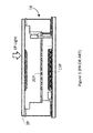
- FIG. 1 shows a conventional, PRIOR ART image capture device with a field emission type electron source 15 and a grid electrode 20 , as shown in the '743 publication.
- the grid electrode 20 positioned between the electron emitting construct (comprising the field emission type electron source 15 ) and the electron receiving construct (comprising the faceplate 3 ), accelerates and directs the electron beams from the field emission type electron sources 15 to a predetermined target area on the electron receiving construct.
- Imaging devices comprising a grid electrode have the disadvantage of having a reduced utilization efficiency of the electron beams being emitted from the electron source.
- a grid electrode e.g., as illustrated in the '507 publication
- electrons that fail to pass through the open area are absorbed into the grid and are lost without providing signal current.
- the size of the grid electrode openings is widened (to increase utilization efficiency of the electron beams)
- another problem arises wherein electrons with an angular (i.e., non-perpendicular) component will pass through and hit the photoconductor outside of the predetermined target location.
- the grid electrode can become a source of microphonic noise in applications where the system must be moved during irradiation such as video imaging, CT scanning or Fluoroscopy.
- the interaction between the electron beam and the grid can create an energy spread in the electron beam, thus changing the system characteristics.
- the disclosure below addresses the above-described problems associated with x-ray emission devices based on field emission type electron sources.
- the embodiments described herein provide an image capture device comprising an electron receiving construct and an electron emitting construct separated by at least one spacer situated such that an inner gap is present between said electron receiving construct and said electron emitting construct.
- the electron receiving construct may comprise a faceplate, an anode and an inward facing photoconductor.
- the electron emission construct may comprise: (a) a backplate, (b) a substrate, (c) a cathode, (d) a plurality of field emission type electron sources arranged in an array, wherein said field emission type electron source is configured to emit an electron beam towards said photoconductor and (e) a gate electrode.
- the inner gap may provide an unobstructed space between the electron emitting construct and the electron receiving construct.
- the image capture device does not comprise a grid electrode.
- the electron emitting construct may further comprise a plurality of first focus structures arranged in an array, each of said first focus structures comprising a first focus electrode.
- the first focus structure may surround a unit cell comprising a subset of said field emission type electron sources, said unit cell defining a pixel.
- the electron emission construct may further comprise a plurality of second focus structures arranged in an array, each of said second focus structures comprising a second focus electrode.
- the photoconductor comprises amorphous Selenium.
- the field emission type electron source is a Spindt-type electron source.
- the image capture device comprises a resistive layer situated between the field emission type electron source and the cathode.
- the field emission type electron source is electrically connected to a driving circuit via a signal line, and the first focus electrode surrounds said signal line.
- the substrate is silicon based.
- At least one member selected from the group consisting of the cathode, the resistive layer, the signal line, the field emission type electron source, the gate electrode, the first focus structure, the first focus electrode and any combination thereof, is integral to the substrate.
- the pixel has the pixel pitch of 100 micrometers ⁇ 100 micrometers or less.
- the distance between the array of field emission type electron sources and the anode is between 50 micrometers and 400 micrometers.
- the distance between the array of field emission type electron sources and the anode is 0.5 to 4.0 times the pixel pitch.
- the embodiments described herein provide an x-ray emitting device comprising an x-ray emitting construct and an electron emitting construct separated by at least one spacer situated such the x-ray emitting construct and the electron emitting construct face each other, and that an evacuated inner gap is present between said electron receiving construct and said electron emitting construct; said x-ray emitting construct comprising an anode, the anode being an x-ray target; and said electron emitting construct comprising at least one active zone, each active zone comprising at least one active area comprising: a cathode; a gated cone electron source, comprising a plurality of emitter tips arranged in an array; a resistive layer situated between the gated cone electron source and the cathode; a gate electrode comprising a plurality of gate holes, the position of at least one of said gate holes corresponding to the position of at least one of said emitter tips; wherein said emitter tip is configured to emit an electron beam towards the x-ray emitting construct.
- the diameter of the gate hole is less than 200 nanometers.
- the width of the base of the emitter tip is less than 300 nanometers.
- the active zone comprises more than one active area.
- the gate electrode is connected to a voltage source through a gate interconnect lead, the gate electrode being situated in a gap of the gate interconnect lead such that the gate electrode is connected on all sides to the gate interconnect lead.
- the gate interconnect lead is thicker than the gate electrode.
- the gate interconnect lead is of a thickness between 0.5 microns and 20 microns. In certain embodiments of the disclosure, the resistive layer is of a thickness greater than 300 nm or between 300 and 5000 nanometers.
- the resistive layer comprises SiCN.
- the resistive layer further comprises a first barrier sublayer situated at the interface with the cathode, a second barrier sublayer situated at the interface with the gated cone electron source, or both first and second barrier sublayers.
- the barrier sublayer comprises SiCN or SiC having a silicon atomic percentage of less than 40%, or comprises amorphous carbon.
- the gated cone electron source is capable of passing an electrical current having a flux density of between 1 and 10 mA/mm 2 .
- the active area is of an area of between 100 square microns and 4 square millimeters.
- the active area comprises between 1 and 10 emitter tips per square micron.
- the cathode is of a thickness between 0.5 microns and 20 microns.
- each of the emitter tips, the corresponding gate hole, the cathode and the resistive layer overlap along the plane of the electron emitting construct.
- the inner gap provides an unobstructed space between said electron emitting construct and said electron receiving construct.
- the anode comprises one or more of the group consisting of molybdenum, rhodium and tungsten.
- the substrate is silicon-based.
- At least one member selected from the group consisting of the gate electrode, the cathode, the resistive layer and the gated cone electron source is integral to the substrate.
- the active zone is enclosed by at least one focus structure.
- the active zone comprises a plurality of active areas and said plurality of active areas is configured to be co-activated.
- the active zone comprises a plurality of active areas, and one or more subsets of said plurality of active areas are capable of being activated independently.
- the total emission current of the active zone is capable of being tuned through the controlled activation of one or more of said active zones.
- said subsets of the plurality of active areas are organized as concentric regions, such that the initial width of the electron beam is capable of being tuned through the controlled activation of one or more of said concentric regions.
- the embodiments described herein provide an x-ray imaging system comprising an image capture device as provided in the first aspect of the disclosure and further comprising an x-ray emitting device as provided in the second aspect of the disclosure.
- FIG. 1 is a schematic diagram representing a PRIOR ART image capture device comprising a grid electrode.
- FIG. 2 is a schematic diagram representing an image capture device according to the present disclosure.
- FIG. 3 is a schematic diagram representing the image capture device further indicating the device thickness a, the pixel pitch b and the pixel size c.
- FIG. 4 is a schematic diagram representing the image capture device comprising an array of second focus structures.
- FIG. 5 is a schematic diagram representing an overhead view of the electron emitting construct.
- FIG. 6 is a schematic diagram representing a side view of an x-ray emitting device incorporating the electron emitting construct.
- FIG. 7 is a schematic diagram representing a side view of an alternative x-ray emitting device incorporating the electron emitting construct.
- FIG. 8 is a schematic diagram representing an overhead view of an electron emitting construct.
- FIGS. 9A-D are schematic diagrams of various embodiments of active areas within an active zone, being activated in various pattern.
- FIG. 10 is schematic diagram representing a side view (along, e.g., line A of FIG. 9A ) of an active area of the electron emitting construct.
- FIGS. 11A-D are schematic diagrams of an x-ray imaging system according to the present disclosure.
- FIG. 12 shows the results of a simulation showing the effect of the width of the distance between the electron emitting construct and the electron receiving construct (Gap) on the width of the area on the photoconductor that is struck by the electron beam from the electron sources of an emitter area (beam landing width).
- FIG. 13 shows the results of a simulation showing the effect of a single focus structure on electron beam trajectory.
- FIG. 14 shows the results of a simulation showing the effect of a double focus structure on electron beam trajectory.
- FIG. 15 is a plot showing the results of a simulation showing the effects of initial electron velocity focus bias on focal spot size.
- FIGS. 2-5 shows an image capture device 100 of the disclosure.
- the image capture device 100 includes an electron emitting construct 110 and an electron receiving construct 120 , separated by a spacer 4 .
- the spacer 4 may be situated such that an inner gap 30 is present between the electron receiving construct 120 and the electron emitting construct 110 .
- the inner gap 30 may be sealed and maintained under vacuum, and may provide an unobstructed space between the electron emitting construct 110 and the electron receiving construct 120 .
- the electron emitting construct 110 may comprise a backplate 5 , a substrate 6 , a cathode 7 , an array of field emission type electron sources 9 and a gate electrode 10 .
- the electron receiving construct 120 may comprise faceplate 1 , an anode 2 and an inward facing photoconductor 3 .
- the electron emitting construct 110 may further comprise a plurality of first focus structures 11 arranged in an array, each of said first focus structures 11 comprising a first focus electrode 12 .
- the electron emitting construct 110 may further comprise a plurality of second focus structures 13 comprising a second focus electrode 14 (see FIG. 4 ).
- the image capture device 100 may further comprise a resistive layer 8 (not shown) situated between the cathode 7 and the field emission type electron sources 9 , in order to regulate the current into the field emission type electron sources 9 .
- the field emission type electron source 9 may be activated to emit an electron beam 20 that is directed towards the photoconductor 3 .
- the field emission type electron source 9 is situated between the anode 2 and the cathode 7 such that the electron beam 20 emitted by the field emission type electron source 9 is accelerated towards the anode 2 .
- the photoconductor 3 may be situated between the field emission-type electron source 9 and the anode 2 , such that the emitted electron beam 20 strikes the photoconductor 3 .
- a grid electrode which is generally situated in a prior art image capture device between the electron emitting construct 110 and the electron receiving construct 120 , is not typically present in the image capture device 100 of the disclosure.
- a grid electrode may be a thin material with an array of small openings having a grid-, mesh- or sieve-like structure, positioned between the anode 2 and the cathode 7 .
- the grid electrode may be referred to as a mesh electrode, a control grid or a trimming electrode.
- the grid electrode 20 lies between the electron emitting construct (comprising the field emission type electron source 15 ) and the electron receiving construct (comprising the faceplate 3 ). In contradistinction, with reference to FIG.
- the inner gap 30 of the image capture device 100 of the disclosure provides an unobstructed space between the electron emitting construct 110 and the electron receiving construct 120 , such that the electron beam 20 emitted from the field emission type electron source 9 travels directly to the photoconductor 3 without traversing any intermediate construction situated between the electron emitting construct 110 and the electron receiving construct 120 .
- the faceplate 1 and anode 2 of the electron receiving construct 120 may be constructed of materials and/or configured that transmits incident electromagnetic radiation radiating from the front of the faceplate 1 , such that the incident electromagnetic radiation reaches the photoconductor 3 .
- Materials used for the photoconductor 3 are known in the art, e.g., amorphous Selenium (a-Se), HgI 2 , PHI 2 , CdZnTe, or PbO.
- the photoconductor 3 comprises amorphous Selenium.
- the electromagnetic radiation may be of any frequency.
- the electromagnetic radiation is in the X-ray frequency range.
- the electromagnetic radiation may be in the visible light frequency range.
- the substrate 6 may be a semiconductor material, for example, crystallized silicon. Further, any one of the cathode 7 , the resistive layer 8 , the field emission type electron source 9 , the gate electrode 10 , the first focus structure 11 , the first focus electrode 12 , the second focus structure 13 , the second focus electrode 14 and the signal line (not shown), or any combination thereof, may be processed on, and integral to, the substrate 6 . In certain embodiments the resistive layer 8 may further be processed on, and integral to, the substrate 6 .
- the field emission type electron source 9 may be electrically connected to a driving circuit via a signal line (not shown) and further electrically connected to a gate electrode 10 .
- the coordinated electrical activation of the driving circuit and the gate electrode 10 connected to a field emission type electron source 9 results in its activation, i.e., electron emission.
- the field emission type electron source 9 performs the electron emission by an electric field formed between the field emission type electron source 9 and the gate electrode 10 .
- the field emission type electron source 9 may be a gated cone electron source having cones (“emitter tips”) arranged in an array, each emitter tip being surrounded by an opening in the gate electrode 10 (a “gate hole”), a Spindt type electron source, a carbon nanotube (CNT) type electron source, a metal-insulator-metal (MIM) type electron source or a metal-insulator-semiconductor (MIS) type electron source.
- the field emission type electron source 9 may be a Spindt type electron source.
- the anode 2 and the cathode 7 are configured to generate an electrical field therebetween.
- This electrical field accelerates the electrons emitted from the field emission type electron source and directs them towards the photoconductor 3 .
- the strength of the electric field between the anode 2 and the cathode 7 may be 0.1 to 2 volts per micrometers, 0.1 to 1.8 volts per micrometers, 0.1 to 1.5 volts per micrometers, 0.1 to 1 volts per micrometers, 0.1 to 0.5 volts per micrometers, about 0.1 volts per micrometers, about 0.2 volts per micrometers, about 0.3 volts per micrometers, about 0.4 volts per micrometers, about 0.5 volts per micrometers, about 0.6 volts per micrometers, about 0.7 volts per micrometers, about 0.8 volts per micrometers, about 0.9 volts per micrometers, about 1 volts per micrometers,
- a field emission type electron source 9 typically emits electrons having a range of trajectories, referred to as the divergence angle, and not all of the electrons are emitted orthogonal to the electron emitting construct 110 .
- the focus structures of the disclosure e.g., first focus structure 11 comprising a first focus electrode 12 and second focus structure 13 comprising a second focus electrode 14 , serve that function.
- a first focus structure 11 may be configured to surround an emitter area 25 , i.e., a unit cell comprising a subset of the plurality of field emission type electron sources 9 .
- the emitter area 25 also defines a pixel size.
- the first focus electrode 12 may be configured to suppress scatter of the electron beams emitted from the corresponding emitter area 25 through the application of a first focus voltage, thus focusing the emitted electron beam.
- the image capture device 100 of the disclosure may further comprise, in the electron emitter construct 110 , an array of second focus structures 13 comprising a second focus electrode 14 .
- Each second focus structure 13 may be adjacent and inward-facing in relation to each of the first focus structures 11 (with first focus electrodes 12 ), such that an electron emitting construct 110 comprises, in aggregate, a double focus structure facing the electron receiving construct 120 .
- the second focus electrode 14 may be configured to further accelerate the electrons emitted from the corresponding emitter area 25 through the application of a second focus voltage, thus further focusing the emitted electron beam.
- the electron emitting construct 110 may comprise additional focus structures, resulting in an aggregate focus structure that is tripled, quadrupled, or the like.
- the focus structures with the focus electrodes may further function as a drain for misdirected electrons.
- the first focus electrode 12 may be positioned to cover a signal line of the driving circuit for the field emission type electron source 9 , thus reducing radiation noise in the signal lines by protecting the signal lines from irradiation by misdirected electrons.
- the first focus structure 11 may surround an emitter area 25 , i.e., a unit cell comprising a subset of said field emission type electron sources 9 .
- the subset of field emission type electron sources 9 within an emitter area 25 may define a pixel for the image capture device 100 .
- Pixel pitch is a specification of a pixel-based image capture device 100 that is known in the art. Pixel pitch may be expressed, e.g., as the distance between adjacent pixels. See, e.g., distance b in FIG. 3 . Pixel size may be expressed as the area, width and length (if rectangular), or diameter (if circular) of, e.g. the emitter area 25 . See, e.g., distance c in FIG. 3 . Smaller pixel size and pixel pitch contribute to a finer resolution of the image that the device of the disclosure captures.
- the thickness of the image capture device 100 may be expressed as, e.g., the distance between a field emission type electron source 9 and the orthogonal position on the anode 2 (shown as distance a in FIG. 3 ).
- the thickness of the device may, alternatively, be expressed as the orthogonal distance between the anode 2 and the cathode 7 , or as the orthogonal distance between any one component of the electron receiving construct 120 (e.g., the faceplate 1 , the anode 2 or the photoconductor 3 ) and any one component of the electron emitting construct 110 (e.g., the field emission type electron source 9 , the cathode 7 , the substrate 6 and the backplate 5 ).
- the image capture device 100 of the disclosure is designed to improve electron utilization efficiency of the image capture device 100 , i.e., to increase the portion of electrons being emitted from the field emission type electron source 9 that strike the predetermined location on the photoconductor 3 .
- each emitter area 25 of the image capture device 100 i.e., the cell comprising a plurality of field emission type electron sources 9 surrounded by a first focus structure 11
- each emitter area 25 may thus require fewer field emission type electron sources and, thus, the pixel size, as well as the pixel pitch, of the image capture device 100 of the disclosure may be made smaller.
- the pixel of the image capture device 100 of the disclosure may be a square pixel with the pixel pitch of, e.g., between 10 micrometers and 1000 micrometers, between 50 micrometers and 200 micrometers, about 50 micrometers, about 75 micrometers, about 100 micrometers, about 125 micrometers, about 150 micrometers or about 200 micrometers.
- the pixel of the image capture device 100 of the disclosure may be a square pixel with the pixel pitch of about micrometers 100 micrometers.
- a thinner image capture device may be desired.
- thinner devices are more difficult to assemble, and the presence of a grid electrode exacerbates the difficulty in assembly.
- the image capture device 100 of the disclosure may be made thinner, or the same thinness may be produced at less cost, when compared to prior art image capture devices that comprise a grid electrode.
- the ratio between pixel pitch and device thickness is the ratio between pixel pitch and device thickness.
- the device thickness e.g., the distance between the cathode 7 and the anode 2
- the ratio between device thickness and pixel pitch is between 0.5 and 4.0.
- the gap between the cathode 7 and the anode 2 would be between 50 and 400 micrometers.
- the the device thickness e.g., the distance between the cathode 7 and the anode 2 , is from 0.5 to 2.0 times the pixel pitch, from 0.5 to 1.5 times the pixel pitch, from 1 to 3 times the pixel pitch, from 1 to 4 times the pixel pitch, about 0.5 times the pixel pitch, about 0.75 times the pixel pitch, about 1 times the pixel pitch, about 1.5 times the pixel pitch, about 1.75 times the pixel pitch, about 2 times the pixel pitch, about 2.25 times the pixel pitch, about 2.5 times the pixel pitch, about 2.75 times the pixel pitch, about 3 times the pixel pitch, about 3.25 times the pixel pitch, about 3.5 times the pixel pitch, about 3.75 times the pixel pitch or about 4 times the pixel pitch.
- the parameters of the field emission type electron source 9 , the dimensions of the focus structures 11 (and 13 ), the voltage loaded to the focus electrodes 12 (and 14 ), and the height of the spacer 4 , and other parameters of the device may be adjusted as needed
- the x-ray emitting device 1000 includes an electron emitting construct 210 and an x-ray emitting construct 220 (also referred to as an “electron receiving construct”) facing each other, separated by at least one spacer 54 .
- the spacer 54 may be situated such that an inner gap 58 is present between the x-ray emitting construct 220 and the electron emitting construct 210 .
- the inner gap 58 may be sealed and maintained under vacuum, and may provide an unobstructed space between the electron emitting construct 210 and the x-ray emitting construct 220 .
- the electron emitting construct 210 may be activated to emit an electron beam 71 that is directed towards the x-ray emitting construct 220 .
- a gated cone electron source incorporated into the electron emitting construct 210 is situated such that the emitted electron beam 71 is accelerated towards an anode 52 of the x-ray emitting construct 220 .
- the x-ray emitting construct 220 is situated to face the electron emitting construct 210 , and includes an anode 52 .
- the anode 52 of the x-ray emitting construct 220 and the cathode of the electron emitting construct 210 are configured to generate an electrical field therebetween. This electrical field accelerates the electrons emitted from the gated cone electron source and directs them towards the anode 52 .
- the anode 52 is capable of emitting x-rays 75 when struck with an electron beam 71 .
- Anodes such as anode 52 are known in the art and may also be referred to as “targets” or “x-ray targets”.
- the anode 52 may be constructed of, for example, molybdenum, rhodium, tungsten, or a combination thereof.
- the X-ray emitting construct 220 may further include a collimator (not shown), on the outward facing side.
- a collimator (not shown), on the outward facing side.
- the x-rays 75 are emitted in a range of directions, such that they radiate from the x-ray emitting construct 220 in a conical fashion.
- Collimators are devices that filter a stream of rays so that only those traveling parallel to a specified direction are allowed through. As such, the lateral spread of the emitted x-rays may be minimized or eliminated.
- a grid electrode has generally been situated between the electron emitting construct 210 and the x-ray emitting construct 220 .
- a grid electrode may be a thin material with an array of small openings having a grid-, mesh- or sieve-like structure.
- the grid electrode may be referred to as a mesh electrode, a control grid or a trimming electrode.
- Such a grid electrode is typically not present in the x-ray emitting device 1000 of the disclosure.
- the inner gap 58 of the x-ray emitting device 1000 of the disclosure provides an unobstructed space between the electron emitting construct 210 and the x-ray emitting construct 220 , such that the emitted electron beam 71 travels directly to the x-ray emitting construct 220 without traversing any intermediate construction situated between the electron emitting construct 210 and the x-ray emitting construct 220 .
- the x-rays 75 produced by the anode 52 upon being struck with the electron beam 71 may be transmitted through the anode (as shown in FIG. 6 ).
- an x-ray emitting device 1000 ′ may be configured such that the electron beam 71 emitted from the electron emitting construct 210 strikes an anode 52 ′ of the x-ray emitting construct 220 ′ that is placed at an angle, say, 45 degrees to the direction of the electron beam 71 .
- the x-rays 75 ′ created by bremsstrahlung may be emitted at 90 degrees to the incident electron beam 71 and exit the device 1000 ′ sideways through a window 59 ′.
- the x-ray emitting device 1000 ′ includes an electron emitting construct 210 ′ and an x-ray emitting construct 220 ′ facing each other, separated by at least one spacer 54 ′.
- the x-ray emitting construct 220 ′ may include an anode 52 ′ and a window 59 ′.
- the spacer 54 ′ may be situated such that an inner gap 58 ′ is present between the x-ray emitting construct 220 ′ and the electron emitting construct 210 ′.
- the inner gap 58 ′ may be sealed and maintained under vacuum, and may provide an unobstructed space between the electron emitting construct 210 and the x-ray emitting construct 220 ′.
- the various options described for the electron emitting construct 210 and its components as described with reference to FIGS. 8-10 hereinbelow are options for the electron emitting constrict 210 incorporated in the x-ray emitting device 1000 ′, the x-ray emitting device 1000 ′, as well as any other device incorporating an electron emitting construct described herein, including image capture devices.
- the disclosure provides an electron emission construct 210 including one or more emission units 90 .
- the emission units 90 may be integrated into a substrate 55 .
- the emission unit 90 may include an active zone 85 comprising one or more active areas 80 , each active area 80 having a gated cone electron source (not shown) and a gate electrode 60 .
- the gated cone electron source may be a field-emission electron source comprising cones (“emitter tips”) arranged in an array, each emitter tip being surrounded by an opening in the gate electrode 60 (a “gate hole”).
- the active areas 80 are connectable to a voltage source VS through a gate interconnect lead 64 , which is conductively connected to the gate electrode(s) 60 , as well as through a cathode 56 , which overlaps with the gate interconnect lead 64 .
- the emission unit 90 may further include a focus structure 95 .
- the emission unit 90 is configured to emit an electron beam upon the activation of the gated cone electron source (not shown) incorporated into the one or more active areas 80 present in the active zone 85 .
- the active areas 80 may be activated by connecting the gate interconnect lead 64 (thus also the gate electrode 60 ) and the cathode 56 to a voltage source VS.
- the resulting exposure of emitter tips, incorporated into the gated cone electron source, to a voltage gradient causes said emitter tips to emit an electron beam.
- a field emission type electron source typically emits electrons having a range of trajectories, referred to as the divergence angle, and not all of the electrons are emitted orthogonal to the electron emission construct 210 .
- the divergence angle a range of trajectories
- the focus structure 95 of the disclosure serves that function.
- the focus structure 95 may be configured to surround an active zone 85 .
- the focus structure 95 may be configured to suppress scatter of the electron beams emitted from the corresponding active zone 85 through the application of a focus voltage on a focus electrode incorporated therein, thus focusing the emitted electron beam.
- the focus structure 95 may comprise a first focus structure and a second focus structure, one being situated on top of the other, such that the focus structure 95 comprises, in aggregate, a double focus structure.
- the second focus electrode may be configured to further accelerate the electrons emitted from the active zone 85 through the application of a second focus voltage, thus further focusing the emitted electron beam.
- the focus structure 95 may comprise, in aggregate, a triple focus structure, a quadruple focus structure, and the like.
- the focus structure 95 may further function as a drain for misdirected electrons.
- the focus structure 95 may be positioned to cover a signal line of the driving circuit for the gated cone electron source, thus reducing radiation noise in the signal lines by protecting the signal lines from irradiation by misdirected electrons.
- each active area 80 may be situated in a fully enclosed gap within the gate interconnect lead 64 . That is, each active area 80 may be an island surrounded by the gate interconnect lead 64 . As such, the gate electrode 60 may be conductively connected to the gate interconnect lead 64 from any or all lateral sides.
- the active zone 85 includes sixteen active areas 80 .
- the active zone 85 may have as many active areas as deemed appropriate for the use of the electron emitting construct 210 .
- there may be as few as one active area 80 as many as a hundred (e.g., 10 ⁇ 10 active areas 80 ), as many as a thousand (e.g., 100 ⁇ 100 active areas 80 ), or more active areas 80 , in the active zone 85 .
- the active areas 80 shown in FIG. 9A are square in shape, the active area 80 may be, variously, rectangular, circular, bent bands, pie-shapes or the like. Similarly, the active area 80 may be, variously, rectangular, circular, bent bands, pie-shapes or the like. In addition, multiple active areas 80 may be arranged in the active zone 85 in a square grid pattern (as shown in FIG. 9A ), a rectangular grip pattern, a radial pattern, or the like.
- the active area 80 may be in a square shape, for example, of about 2 mm ⁇ 2 mm, about 1.5 mm ⁇ about 1.5 mm, about 1.0 mm ⁇ 1.0 mm, about 750 microns ⁇ 750 microns, about 500 microns ⁇ 500 microns, about 400 microns ⁇ 400 microns, about 300 microns ⁇ 300 microns, about 200 microns ⁇ 200 microns, about 150 microns ⁇ 150 microns, about 100 microns ⁇ 100 microns, about 75 microns ⁇ 75 microns, about 50 microns ⁇ 50 microns, about 25 microns ⁇ 25 microns, about 10 microns ⁇ 10 microns, or between 75 microns and 125 microns.
- An active area 80 having dimensions about 2 mm ⁇ 2 mm has a size (i.e., surface area) of about 4 square millimeters (mm 2 ), an active area 80 having dimensions of about 10 microns ⁇ 10 microns has a size of about 100 square microns, and so forth.
- the size of the active zone 85 depends on the size of the active area 80 and the number of active areas 80 within the active zone 85 , as well as the width of the portion of the gate interconnect lead 64 interspersed between, and surrounding, each active area. Typically, the dimensions of the active zone 85 may be about 10-20% greater than the aggregate dimensions of the active areas 80 along the same side, due to the interspersed portions of the gate interconnect lead 64 .
- the active zone 85 may have a size of about 480 microns by 480 microns (in a case where the interspersed portions of the gate interconnect lead 64 adds 20% to the width of the active zone).
- the emission unit may be configured such that all active areas 80 of the active zone 85 are configured to be co-activated.
- each active area 80 (or different subsets of active areas 80 ) within an active zone 85 may be capable of being activated independently, that is, an individual active area 80 , or a subset of the active areas 80 , may be activated while the remaining active areas 80 within the active zone 85 remain inactive.
- the active areas 80 may be activated in various spatial and temporal patterns. As such, subsets of active areas 80 may be activated to realize different emission currents for the active zone 85 .
- subsets of active areas 80 encompassing different concentric regions of the active zone 85 may be activated separately to realize different sizes of the initial width, e.g., the cross-sectional area, of the emitted electron beam by the active zone 85 , and, thus, the focal spot size of the emitted electron beam.
- the emission current of the electron beam emitted by the active zone 85 may be capable of being tuned through the controlled activation of one or more of the active areas 80 within the active zone 85
- the initial width of the electron beam emitted by the active zone 85 may be capable of being tuned through the controlled activation of one or more subsets of the active areas 80 organized as concentric regions.
- an active zone having nine active areas arranged in a 3 ⁇ 3 grid may be divided into two concentric regions, the first concentric region encompassing the central active area and the second concentric region encompassing the outer eight active areas.
- an active zone having twenty-five active areas arranged in a 5 ⁇ 5 grid may be divided into three concentric regions, the first concentric region encompassing the central active area, the second concentric regions encompassing the eight intermediate active areas, and the third concentric region encompassing the sixteen outer active areas. It will be appreciated that an active zone may be configured to have a yet larger array of active areas, having, e.g., four, five, six or more concentric regions.
- said active zone 85 ′ may have three concentric regions that are separately activatable: a first region including the center active area 80 M′; a second concentric region including the intermediate active areas 80 G′, 80 H′, 80 I′, 80 L′, 80 N′, 80 Q′, 80 R′ and 80 S′; and a third concentric region including the outer active areas 80 A′- 80 E′, 80 F′, 80 J′, 80 K′, 80 O′, 80 P′, 80 T′ and 80 U′- 80 Y′. As shown in FIG.
- the above disclosure in relation to FIGS. 9A-D , provides for methods of tuning the emission current and/or the initial width of an electron beam emitted by an active zone comprising multiple active areas. It will further be appreciated that said methods may be applied to active areas having any type of electron source, and are not limited active areas having a gated cone electron source. As such, the above-described methods may be applied to, for example, a Spindt type electron source, a carbon nanotube (CNT) type electron source, a metal-insulator-metal (MIM) type electron source or a metal-insulator-semiconductor (MIS) type electron source.
- CNT carbon nanotube
- MIM metal-insulator-metal
- MIS metal-insulator-semiconductor
- an active area 80 of the electron emitting construct 210 may comprise a substrate 55 , a cathode 56 , a resistive layer 57 , a gated cone electron source 70 , and a gate electrode 60 .
- the active area 80 may be defined as the area occupied by the gated cone electron source 70 and/or the corresponding gate electrode 60 .
- the active area 80 may also be defined as the area enclosed by the gate interconnect lead 64 .
- the gated cone electron source 70 may comprise a plurality of emitter tips 72 arranged in an array.
- the gated cone electron source 70 may further comprise an interlevel dielectric (ILD) layer 74 having a plurality of ILD windows, with an emitter tip 72 being situated at each ILD window.
- the ILD 74 may further serve as a support for the gate electrode 60 situated thereupon.
- the emitter tip 72 may be constructed of, e.g., chromium, molybdenum or the like. Each emitter tip 72 may be about 500 nanometers (nm), about 400 nm, about 300 nm, about 200 nm, about 100 nm, less than 500 nm, less than 400 nm, less than 300 nm, less than 200 nm, less than 100 nm, between 100 and 300 nm, or between 200 and 400 nm in height.
- Each emitter tip may be about 500 nm, about 400 nm, about 300 nm, about 200 nm, about 100 nm, less than 500 nm, less than 400 nm, less than 300 nm, less than 200 nm, less than 100 nm, between 100 and 300 nm, or between 200 and 400 nm in width at the base.
- the emitter tip 72 may be less than 300 nm in height and less than 300 nm in width at the base.
- the gate electrode 60 may comprise a plurality of gate holes 62 .
- the gate electrode 60 may be constructed out of a conductive material such as chromium, niobium or the like.
- the position of the gate holes 62 corresponds to the position of the ILD windows and the emitter tips 72 , such that each emitter tip is configured to emit an electron beam outwards out of the gate hole 62 .
- the gate hole 62 may have a diameter of between 50 and 500 nanometers, between 100 and 400 nanometers, between 150 and 250 nanometers, about 100 nanometers, about 150 nanometers, about 175 nanometers, about 200 nanometers, about 225 nanometers, about 250 nanometers, about 300 nanometers, about 350 nanometers, less than 300 nanometers, less than 250 nanometers, less than 200 nanometers, less than 150 nanometers, and less than 100 nanometers.
- the gate electrode 60 may be conductively connected to a voltage source via the gate interconnect lead 64 .
- the gate electrode 60 may have a thickness of about 50 nanometers (nm), about 60 nm, about 70 nm, about 80 nm, about 90 nm, about 100 nm, about 125, between 50 nm and 125 nm or between 80 nm and 100 nm.
- the gate interconnect lead 64 may have a thickness of between 0.5 microns and 20 microns. As such, the gate electrode 60 is thinner than the gate interconnect lead 64 . Due to the thinness, as well as the presence of the gate holes 62 , the resistance of the gate electrode 60 is substantially higher than the resistance of the gate interconnect lead 64 .
- the resistive layer 57 is situated between the cathode 57 and the gated cone electron source 70 , and serves to regulate the electric current that flows between the cathode 57 and the emitter tips 72 during their activation, among other functions.
- the resistive layer 57 may comprise silicon carbon nitride (SiCN), silicon carbide or amorphous silicon.
- the resistive layer 57 may further comprise a barrier sublayer at one or more of its exterior surface. That is, the resistive layer 57 may comprise a barrier sublayer situated at the interface with the cathode, at the interface with the gated cone electron source, or situated at both the cathode interface and the gated cone electron source interface.
- the barrier sublayer may comprise a carbon-rich SiCN layer or a nitrogen-rich SiCN layer.
- SiCN encompasses a wide range of compositions.
- SiCN may be represented by Si(x)C(y)N(z), where x, y, z shows the atomic percentage of each element.
- This notation of SiCN includes cases where the atomic percentage is 0.
- SiC silicon carbide
- a nitride-rich or carbon-rich barrier layer may be SiCN with a higher y value (carbon atomic percentage) or a higher z value (nitrogen atomic percentage) in comparison to the Si(x)C(y)N(z) utilized in the resistive layer 57 .
- the nitride-rich or carbon-rich barrier layer may be SiCN or SiC having a silicon atomic percentage of less than 40%.
- the carbon-rich barrier layer may be amorphous carbon.
- the x, y and z values for Si(x)C(y)N(z) compositions can be controlled by various methods known in the art, e.g., deposition conditions using sputter of chemical vapor deposition (CVD).
- the cathode 56 may comprise copper (Cu) or aluminum (Al), and may be of a thickness of between 0.5 microns and 20 microns.
- the gated cone electron source 70 , the resistive layer 57 and the cathode 56 are vertically aligned. That is, the gate electrode 60 , gated cone electron source 70 , the resistive layer 57 and the cathode 56 all overlap each other along the plane of active area 80 and the electron emitting construct 210 . Further, the position of each of the emitter tips 72 , the corresponding gate hole 62 , the cathode 56 and the resistive layer 57 may overlap along the plane of the electron emitting construct.
- Such an arrangement presents little or no lateral displacement between each of the above components, and results in (among other effects): maintaining the uniformity of the voltage gradient between the gate electrode 60 and the cathode 56 ; and maintaining the uniformity of the path of, and the resistances encountered by, the electrical current provided to each individual emitter tip 72 .
- the substrate 55 may comprise a semiconductor material, for example, crystallized silicon. Further, any one of the cathode 56 , the resistive layer 57 , the gated cone electron source 70 including the emitter tip 72 and the ILD 74 , the gate electrode 60 , the lead interconnect lead 64 or any combination thereof, may be processed on, and integral to, the substrate 55 .
- the present disclosure further provides for an X-ray imaging system comprising at least one x-ray emitting device as described herein and at least one image capture device as described herein, situated such that the x-ray emitting device emits an x-ray beam towards the electron receiving construct of the image capture device, which may include a photoconductor.
- FIG. 11A shows an x-ray imaging system 2000 , comprising an image capture device 100 and an x-ray emitting device 1000 ′.
- the image capture device 100 includes an electron emitting construct 110 and an electron receiving construct 120 , separated by a spacer 4 .
- the spacer 4 may be situated such that an inner gap 30 is present between the electron receiving construct 120 and the electron emitting construct 110 .
- the inner gap 30 may be sealed and maintained under vacuum, and may provide an unobstructed space between the electron emitting construct 110 and the electron receiving construct 120 .
- the electron receiving construct 110 may comprise a photoconductor, and be configured to receive x-rays emitted by the x-ray emitting device 1000 ′.
- the image capture device 100 and its components are described in further detail elsewhere herein.
- the x-ray emitting device 1000 ′ may be configured such that the electron beam 71 emitted from the electron emitting construct 210 strikes an anode 52 ′ of the x-ray emitting construct 220 ′ that is placed at an angle, say, 45 degrees to the direction of the electron beam 71 .
- the x-rays 75 ′ created by bremsstrahlung may be emitted at 90 degrees to the incident electron beam 71 and exit the device 1000 ′ sideways through a window 59 ′.
- the x-ray emitting device 1000 ′ and its components are described in further detail elsewhere herein.
- the x-ray imaging system 2000 is configured to allow an object 300 to be placed between the x-ray emitting device 1000 ′ and the image capture device 100 , such that the x-rays 75 ′ (or a portion thereof) traverse the object 300 (or a portion thereof) before striking the image capture device 100 (or a portion thereof), thereby producing an x-ray transmission image of the object 300 .
- the power and/or width of the x-ray emitting by the x-ray emitting device 1000 ′ in the x-ray imaging system 2000 may be tunable.
- FIGS. 11B-D showing the x-ray imaging system 2000 with an expanded view of an active zone 85 ′ incorporated into the electron emitting construct 210 , having twenty-five active areas 80 A′- 80 Y′ arranged in a 5 ⁇ 5 grid pattern.
- the active zone 85 ′ may have, for example, three concentric regions that are separately activatable: a first region including the center active area 80 M′; a second concentric region including the intermediate active areas 80 G′, 80 H′, 80 I′, 80 L′, 80 N′, 80 Q′, 80 R′ and 80 S′; and a third concentric region including the outer active areas 80 A′- 80 E′, 80 F′, 80 J′, 80 K′, 80 O′, 80 P′, 80 T′ and 80 U′- 80 Y′.
- activating the first concentric region (the activated active areas 80 ′ being shown in white) while keeping the second and third concentric regions inactive (the inactive active areas 80 ′ being shown in black) will result in the emission of a narrow electron beam with a small emission current, such that the x-ray emitting device 1000 ′ emits a narrow x-ray beam ( FIG. 11B ).
- activating the first and second concentric regions together, while keeping the third concentric region inactive will result in the emission of an electron beam of intermediate width with an intermediate emission current, such that the x-ray emitting device 1000 ′ emits an x-ray beam of intermediate width ( FIG. 11C ).
- an x-ray imaging system may comprise any x-ray emitting device as described herein, for example, as shown in and described in reference to FIGS. 6-10 , and may comprise any image capture device as described herein, for example, as shown in and described in reference to FIGS. 2-5 . It will be further appreciated that an x-ray imaging system, as provided in the present disclosure, may comprise multiple x-ray emitting devices and/or multiple image capture devices.
- the active area 80 and the corresponding gate electrode 60 may be surrounded by portions of the gate interconnect lead 64 . That is, the gate electrode 60 of an active area 80 may be situated in a fully enclosed gap within the gate interconnect lead 64 .
- the above-described arrangement of having multiple active areas 80 has various advantages, for example reducing the path length of an electric current through the high-resistance gate electrode 60 which may improve the uniformity of the voltage gradient between the gate electrode 60 and the cathode 56 along the plane of the gated cone electron source 70 .
- this arrangement has the added effect of evening out the temperature distribution of the active zone 85 , as the gate interconnect lead 64 may be a better heat conductor than the gate electrode 60 .
- the gated cone electron source 70 may be considered to be a nano gated cone electron source. It is particularly noted that the small size of the individual elements of the gated cone electron source 70 , e.g., the emitter tips 72 , in combination with the small diameter of the gate holes 62 , allows for the placement of a large number of emitter tips 72 in each active area 80 and thus in each active zone 85 .
- the active area 80 may include about 1 emitter tip 72 per square micron.
- the small size of the emitter tips 72 and the gate holes 62 may allow for the placement of about 10,000 emitter tips 72 .
- the gated cone electron source 70 may have an emitter tip density that is higher than one emitter tip 72 per square micron, e.g., between one and ten emitter tips 72 per square micron, between two and four emitter tips per square micron, or the like.
- the small size of the emitter tips 72 and gate holes 62 enables a high density of emitter tips 72 to produce high flux density through the gated cone electron source 70 while allowing the current passing through each emitter tip 72 to be low, thus also resulting in improved lifespan, stability and uniformity in the function of the gated cone electron source.
- the gated cone electron source 70 may be capable of passing an electrical current having a flux density (i.e., may be capable of having an emission current density) of between 1 and 10 mA/mm 2 (milliAmperes per square millimeter).
- the gated cone electron source 70 may be configured to emit an electron beam with an initial velocity of about 5 eV, about 10 eV, about 15 eV, about 20 eV or between 5 and 15 eV.
- the emission current of an active area 80 will depend on its size (e.g. the surface area). Similarly, the emission current of an active zone 85 will depend on the number of active areas 80 it contains. For example, an active area 80 of 100 microns ⁇ 100 microns in size, having an emission current density of 10 mA/mm 2 , has an emission current of 0.1 mA. As such, an active zone that is 1.1 mm 2 in size, having 100 such active areas 80 , has an emission current of 10 mA. Similarly, an active zone that is 11 mm 2 in size, having 1000 such active areas 80 , has an emission current of 100 mA.
- an active zone that is 55 mm 2 in size, having 5000 such active areas 80 has an emission current of 500 mA. Therefore, the emission current of the active zone 85 may be as low as 10 mA, or as much as 500 mA, or higher.
- the cathode 56 may be configured to pass a current (a “cathode current”) of about 10 mA, about 50 mA, about 100 mA, about 200 mA, about 300 mA, about 400 mA, about 500 mA, about 600 mA, about 700 mA, about 800 mA, about 900 mA, about 1 A, more than 800 mA, between 500 and 700 mA, between 300 mA and 800 mA, between 100 mA and 800 mA, between 10 mA and 1 A, at least 500 mA at least 600 mA, at least 700 mA or at least 800 mA.
- a current a “cathode current”
- the cathode current may comprise the emission current of the corresponding active zone 85 (as described above) and a gate leakage current through the corresponding gate electrodes 60 (and the corresponding gate interconnect lead 64 ).
- the gate leakage current is small in comparison to the emission current, and as such, the cathode current is similar to, or slightly higher than, the emission current of the active zone 85 .
- the x-ray emitting device may be arranged in various geometries to satisfy a range of x-ray system configurations, including CT scanners, cone beam CT, electron beam CT, other tomographic modalities including breast tomosynthesis tomography, reverse geometry x-ray configurations (in which an extended x-ray source which can emit x-rays from various positions quickly is placed close to the patient, and the x-ray detector is placed far from the patient) and other configurations which require rapid switching between stationary x-ray sources placed in various locations around the patient.
- CT scanners cone beam CT
- electron beam CT other tomographic modalities including breast tomosynthesis tomography
- reverse geometry x-ray configurations in which an extended x-ray source which can emit x-rays from various positions quickly is placed close to the patient, and the x-ray detector is placed far from the patient
- other configurations which require rapid switching between stationary x-ray sources placed in various locations around the patient.
- FIG. 12 shows the results from a simulated image capture device depicting how the width of an electron beam at the point where it strikes the opposing surface of an electron receiving construct facing it (e.g., a photoconductor in the case of an image capture device of the disclosure or an x-ray target in the case of an x-ray emitting device of the disclosure), increases as the gap between the electron emitting construct and the electron receiving construct increases.
- the beam landing width, or the focal spot size refers to the width of an electron beam at the point where it strikes the electron receiving construct facing it
- the gap refers to the distance between the anode (on the electron receiving construct) and the cathode (on the electron emitting construct).
- the beam landing width remain narrow.
- the focal spot size is not more than the pixel pitch, so that the electron beam emitted from one emitter area does not overlap with the electron beam emitted from an adjacent emitter area.
- the pixel pitch that can be achieved within a certain gap distance is limited.
- the focus structures/electrodes serve to restrict the widening of the beam landing width with gap distance, thus e.g., enabling smaller pixel pitch with a larger gap (e.g., between anode and cathode).
- the presence of a first focus structure and the application of a first focus voltage across a first focus electrode may restrict the beam landing width.
- the beam landing width was restricted to about 100 micrometers, in order to match the target pixel pitch of 100 micrometers, with the application of about 30 volts to the first focus electrode (cathode basis).
- the beam landing width was restricted to about 100 micrometers with the application of about 22.5 volts (between 20 and 25 volts) to the first focus electrode.
- the optimal first focus voltage depends on the size of the gap (e.g., anode to cathode distance), as well as with other of parameters including the specifications of the field emission type electron source, the dimensions of the focus structure, and other parameters of the device, which may be adjusted as needed.
- the results of the single focus simulation are shown below in Table 1.
- the further presence of a second focus structure in combination with the first focus structure may further restrict the beam landing width.
- the beam landing width was restricted to about 100 micrometers, in order to match the target pixel pitch of 100 micrometers, with the application of about 600 volts to the second focus electrode (cathode basis) in combination with the application of 30 volts to the first focus electrode (cathode basis).
- the beam landing width was restricted to about 100 micrometers with the application of about 1000 volts to the second focus electrode in combination with the application of 30 volts to the first focus electrode.
- the optimal second focus voltage depends on the size of the gap (e.g., anode to cathode distance), as well as with other of parameters including the specifications of the field emission type electron source, the dimensions of the focus structure, and other parameters of the device, which may be adjusted as needed.
- Table 2 The results of the double focus simulation are shown below in Table 2.
- FIG. 15 shows the results of a simulated device having an electron emitting construct and an electron receiving construct (e.g., an image capture device or an x-ray emitting device) depicting how the width of an electron beam, at the point where it strikes an anode facing it (i.e., the focal spot size), increases as the initial electron velocity of the electron beam emitted from a gated cone electron source increases from 0 eV to 50 eV.
- an electron receiving construct e.g., an image capture device or an x-ray emitting device
- a focal spot size of less than 1000 microns was achieve with an initial electron velocity of 10 eV and a focus bias (the voltage applied to the focus structure) of ⁇ 4000V.
- composition or method may include additional ingredients and/or steps, but only if the additional ingredients and/or steps do not materially alter the basic and novel characteristics of the claimed composition or method.
- a compound or “at least one compound” may include a plurality of compounds, including mixtures thereof.
- range such as from 1 to 6 should be considered to have specifically disclosed subranges such as from 1 to 3, from 1 to 4, from 1 to 5, from 2 to 4, from 2 to 6, from 3 to 6 etc., as well as individual numbers within that range, for example, 1, 2, 3, 4, 5, and 6 as well as non-integral intermediate values. This applies regardless of the breadth of the range.
Priority Applications (1)
| Application Number | Priority Date | Filing Date | Title |
|---|---|---|---|
| US14/385,503 US10242836B2 (en) | 2012-03-16 | 2013-03-14 | Devices having an electron emitting structure |
Applications Claiming Priority (4)
| Application Number | Priority Date | Filing Date | Title |
|---|---|---|---|
| US201261611990P | 2012-03-16 | 2012-03-16 | |
| US201261747455P | 2012-12-31 | 2012-12-31 | |
| US14/385,503 US10242836B2 (en) | 2012-03-16 | 2013-03-14 | Devices having an electron emitting structure |
| PCT/IB2013/052045 WO2013136299A1 (en) | 2012-03-16 | 2013-03-14 | Devices having an electron emitting structure |
Related Parent Applications (1)
| Application Number | Title | Priority Date | Filing Date |
|---|---|---|---|
| PCT/IB2013/052045 A-371-Of-International WO2013136299A1 (en) | 2012-03-16 | 2013-03-14 | Devices having an electron emitting structure |
Related Child Applications (1)
| Application Number | Title | Priority Date | Filing Date |
|---|---|---|---|
| US16/285,475 Continuation US11101095B2 (en) | 2012-03-16 | 2019-02-26 | Devices having an electron emitting structure |
Publications (2)
| Publication Number | Publication Date |
|---|---|
| US20150092923A1 US20150092923A1 (en) | 2015-04-02 |
| US10242836B2 true US10242836B2 (en) | 2019-03-26 |
Family
ID=49160326
Family Applications (2)
| Application Number | Title | Priority Date | Filing Date |
|---|---|---|---|
| US14/385,503 Active 2033-10-28 US10242836B2 (en) | 2012-03-16 | 2013-03-14 | Devices having an electron emitting structure |
| US16/285,475 Active US11101095B2 (en) | 2012-03-16 | 2019-02-26 | Devices having an electron emitting structure |
Family Applications After (1)
| Application Number | Title | Priority Date | Filing Date |
|---|---|---|---|
| US16/285,475 Active US11101095B2 (en) | 2012-03-16 | 2019-02-26 | Devices having an electron emitting structure |
Country Status (7)
| Country | Link |
|---|---|
| US (2) | US10242836B2 (ko) |
| EP (1) | EP2826056B1 (ko) |
| JP (2) | JP2015515091A (ko) |
| KR (1) | KR102076380B1 (ko) |
| CN (1) | CN104170050B (ko) |
| IL (1) | IL234669B (ko) |
| WO (1) | WO2013136299A1 (ko) |
Cited By (4)
| Publication number | Priority date | Publication date | Assignee | Title |
|---|---|---|---|---|
| US20170245814A1 (en) * | 2014-10-16 | 2017-08-31 | Adaptix Ltd | A method of designing an x-ray emitter panel |
| US20190189383A1 (en) * | 2012-03-16 | 2019-06-20 | Nanox Imaging Plc | Devices having an electron emitting structure |
| US11282668B2 (en) * | 2016-03-31 | 2022-03-22 | Nano-X Imaging Ltd. | X-ray tube and a controller thereof |
| US11719652B2 (en) * | 2020-02-04 | 2023-08-08 | Kla Corporation | Semiconductor metrology and inspection based on an x-ray source with an electron emitter array |
Families Citing this family (9)
| Publication number | Priority date | Publication date | Assignee | Title |
|---|---|---|---|---|
| JP6295254B2 (ja) * | 2012-08-16 | 2018-03-14 | ナノックス イメージング ピーエルシー | X線放出装置 |
| JP6476183B2 (ja) | 2013-11-27 | 2019-02-27 | ナノックス イメージング ピーエルシー | イオン爆撃抵抗性を有して構成される電子放出構造物 |
| US10453579B2 (en) * | 2015-02-05 | 2019-10-22 | Shimadzu Corporation | X-ray generator |
| US10334712B2 (en) | 2015-11-11 | 2019-06-25 | Electronics And Telecommunications Research Institute | Radiography apparatus |
| CN109411312B (zh) * | 2018-10-31 | 2020-07-28 | 中国工程物理研究院流体物理研究所 | 基于飞秒激光调制的超快电子枪及其验证方法 |
| CN109507215B (zh) * | 2018-11-26 | 2022-05-17 | 国家纳米科学中心 | X射线成像装置及x射线成像方法 |
| US10825634B2 (en) * | 2019-02-21 | 2020-11-03 | Varex Imaging Corporation | X-ray tube emitter |
| US11152183B2 (en) * | 2019-07-15 | 2021-10-19 | Sigray, Inc. | X-ray source with rotating anode at atmospheric pressure |
| US11417492B2 (en) | 2019-09-26 | 2022-08-16 | Kla Corporation | Light modulated electron source |
Citations (84)
| Publication number | Priority date | Publication date | Assignee | Title |
|---|---|---|---|---|
| GB1467487A (en) | 1973-02-28 | 1977-03-16 | Siemens Ag | X-ray tubes |
| JPH0729507A (ja) | 1993-07-13 | 1995-01-31 | Hitachi Ltd | 撮像管およびその動作方法 |
| US5528103A (en) * | 1994-01-31 | 1996-06-18 | Silicon Video Corporation | Field emitter with focusing ridges situated to sides of gate |
| US5552659A (en) * | 1994-06-29 | 1996-09-03 | Silicon Video Corporation | Structure and fabrication of gated electron-emitting device having electron optics to reduce electron-beam divergence |
| US5587623A (en) | 1993-03-11 | 1996-12-24 | Fed Corporation | Field emitter structure and method of making the same |
| US5635789A (en) | 1992-04-02 | 1997-06-03 | Nec Corporation | Cold cathode |
| WO1997023002A1 (en) | 1995-12-20 | 1997-06-26 | Advanced Technology Materials, Inc. | Integrated circuit devices and methods employing amorphous silicon carbide resistor materials |
| US5677539A (en) * | 1995-10-13 | 1997-10-14 | Digirad | Semiconductor radiation detector with enhanced charge collection |
| JPH10302688A (ja) | 1997-04-30 | 1998-11-13 | Rigaku Corp | X線発生装置 |
| US5892321A (en) | 1996-02-08 | 1999-04-06 | Futaba Denshi Kogyo K.K. | Field emission cathode and method for manufacturing same |
| US5905264A (en) * | 1996-08-14 | 1999-05-18 | Imarad Imaging Systems Ltd. | Semiconductor detector |
| US5929557A (en) | 1996-11-01 | 1999-07-27 | Nec Corporation | Field-emission cathode capable of forming an electron beam having a high current density and a low ripple |
| US6002199A (en) * | 1997-05-30 | 1999-12-14 | Candescent Technologies Corporation | Structure and fabrication of electron-emitting device having ladder-like emitter electrode |
| US6013986A (en) | 1997-06-30 | 2000-01-11 | Candescent Technologies Corporation | Electron-emitting device having multi-layer resistor |
| JP2000048743A (ja) | 1998-05-26 | 2000-02-18 | Futaba Corp | 平面形撮像装置及びその製造方法 |
| US6028313A (en) * | 1997-12-31 | 2000-02-22 | Mcdaniel; David L. | Direct conversion photon detector |
| US6034373A (en) * | 1997-12-11 | 2000-03-07 | Imrad Imaging Systems Ltd. | Semiconductor radiation detector with reduced surface effects |
| US6259765B1 (en) * | 1997-06-13 | 2001-07-10 | Commissariat A L'energie Atomique | X-ray tube comprising an electron source with microtips and magnetic guiding means |
| US6333968B1 (en) * | 2000-05-05 | 2001-12-25 | The United States Of America As Represented By The Secretary Of The Navy | Transmission cathode for X-ray production |
| US6456691B2 (en) * | 2000-03-06 | 2002-09-24 | Rigaku Corporation | X-ray generator |
| US20030044519A1 (en) | 2001-06-14 | 2003-03-06 | Hyperion Catalysis International, Inc. | Field emission devices using ion bombarded carbon nanotubes |
| US6553096B1 (en) * | 2000-10-06 | 2003-04-22 | The University Of North Carolina Chapel Hill | X-ray generating mechanism using electron field emission cathode |
| US20030201954A1 (en) | 2002-04-26 | 2003-10-30 | Hansen Ronald L. | System and method for recalibrating flat panel field emission displays |
| US6674837B1 (en) * | 2001-06-15 | 2004-01-06 | Nan Crystal Imaging Corporation | X-ray imaging system incorporating pixelated X-ray source and synchronized detector |
| US6760407B2 (en) * | 2002-04-17 | 2004-07-06 | Ge Medical Global Technology Company, Llc | X-ray source and method having cathode with curved emission surface |
| US6807248B2 (en) * | 2001-02-28 | 2004-10-19 | Mitsubishi Heavy Industries, Ltd. | Multisource type X-ray CT apparatus |
| US6980627B2 (en) * | 2000-10-06 | 2005-12-27 | Xintek, Inc. | Devices and methods for producing multiple x-ray beams from multiple locations |
| US7082182B2 (en) * | 2000-10-06 | 2006-07-25 | The University Of North Carolina At Chapel Hill | Computed tomography system for imaging of human and small animal |
| US7085352B2 (en) * | 2004-06-30 | 2006-08-01 | General Electric Company | Electron emitter assembly and method for generating electron beams |
| US7085351B2 (en) * | 2000-10-06 | 2006-08-01 | University Of North Carolina At Chapel Hill | Method and apparatus for controlling electron beam current |
| US7192031B2 (en) * | 2004-02-05 | 2007-03-20 | General Electric Company | Emitter array configurations for a stationary CT system |
| US7227924B2 (en) | 2000-10-06 | 2007-06-05 | The University Of North Carolina At Chapel Hill | Computed tomography scanning system and method using a field emission x-ray source |
| JP2007194014A (ja) | 2006-01-18 | 2007-08-02 | Fujifilm Corp | 画像検出器 |
| US20070235772A1 (en) | 2004-10-06 | 2007-10-11 | Sungho Jin | Field emitter array with split gates and method for operating the same |
| US20070246789A1 (en) | 2006-04-21 | 2007-10-25 | Joerg Freudenberger | Thermionic flat electron emitter |
| JP2007305337A (ja) | 2006-05-09 | 2007-11-22 | Hitachi Medical Corp | マイクロフォーカスx線管 |
| US7323692B2 (en) | 2004-08-10 | 2008-01-29 | Research Foundation Of State University Of New York | Flat-panel detector with avalanche gain |
| US20080043920A1 (en) | 2000-10-06 | 2008-02-21 | The University Of North Carolina At Chapel Hill | Micro-focus field emission x-ray sources and related methods |
| US7348531B2 (en) | 2004-02-12 | 2008-03-25 | Pioneer Corporation | Photoelectric conversion device and image pickup device using electron emission devices |
| US20080135766A1 (en) | 2005-02-01 | 2008-06-12 | Sang Hee Nam | Digital X-Ray Image Detector Using an Fed Device |
| US20080211401A1 (en) | 2004-12-17 | 2008-09-04 | Tomonari Nakada | Electron Emission Device And Manufacturing Method Of The Same |
| WO2008136188A1 (ja) * | 2007-04-26 | 2008-11-13 | Panasonic Corporation | X線撮像デバイス及びx線撮影装置 |
| US20090096393A1 (en) | 2007-10-16 | 2009-04-16 | Masateru Taniguchi | Electron-Emissive Element and Display Element |
| US7548018B2 (en) * | 2004-08-30 | 2009-06-16 | Samsung Sdi Co., Ltd. | Electron emission device with a grid electrode for focusing electron beams |
| US20090185660A1 (en) | 2008-01-21 | 2009-07-23 | Yun Zou | Field emitter based electron source for multiple spot x-ray |
| JP2009272289A (ja) | 2006-02-15 | 2009-11-19 | Panasonic Corp | 電界放出型電子源装置及びその駆動方法 |
| US7627087B2 (en) * | 2007-06-28 | 2009-12-01 | General Electric Company | One-dimensional grid mesh for a high-compression electron gun |
| US20100025568A1 (en) | 2008-07-16 | 2010-02-04 | Pioneer Corporation | Image sensing device |
| US7696680B2 (en) * | 2005-02-25 | 2010-04-13 | Tsinghua University | Field emission device for high resolution display |
| US7723664B2 (en) | 2007-05-21 | 2010-05-25 | Nippon Hoso Kyokai | Imaging apparatus having electron source array |
| US7801277B2 (en) * | 2008-03-26 | 2010-09-21 | General Electric Company | Field emitter based electron source with minimized beam emittance growth |
| US7825591B2 (en) * | 2006-02-15 | 2010-11-02 | Panasonic Corporation | Mesh structure and field-emission electron source apparatus using the same |
| US7826594B2 (en) * | 2008-01-21 | 2010-11-02 | General Electric Company | Virtual matrix control scheme for multiple spot X-ray source |
| US7834308B2 (en) | 2007-05-21 | 2010-11-16 | Nippon Hoso Kyokai | Imaging apparatus having electron source array that emits electrons during a blanking period |
| US20100290593A1 (en) | 2008-01-25 | 2010-11-18 | Thales | X-rays source comprising at least one electron source combined with a photoelectric control device |
| US7873146B2 (en) * | 2006-03-03 | 2011-01-18 | Canon Kabushiki Kaisha | Multi X-ray generator and multi X-ray imaging apparatus |
| JP2011071022A (ja) | 2009-09-28 | 2011-04-07 | Horizon:Kk | 電子放出装置及びそれを用いた電子放出型電子機器 |
| JP4693884B2 (ja) | 2008-09-18 | 2011-06-01 | キヤノン株式会社 | マルチx線撮影装置及びその制御方法 |
| US7991120B2 (en) * | 2008-02-28 | 2011-08-02 | Canon Kabushiki Kaisha | Multi X-ray generating apparatus and X-ray imaging apparatus |
| US20110305314A1 (en) | 2010-06-10 | 2011-12-15 | Canon Kabushiki Kaisha | Electron emitting device, image display apparatus using the same, radiation generation apparatus, and radiation imaging system |
| CN102324350A (zh) | 2011-08-07 | 2012-01-18 | 张研 | 一种定向生长的网格状高性能碳纳米管场发射阵列 |
| CN202126987U (zh) | 2011-06-17 | 2012-01-25 | 上海现代科技发展有限公司 | 微焦点x射线源 |
| US8155273B2 (en) * | 2006-02-16 | 2012-04-10 | Stellar Micro Devices | Flat panel X-ray source |
| US8274205B2 (en) * | 2006-12-05 | 2012-09-25 | General Electric Company | System and method for limiting arc effects in field emitter arrays |
| US8428221B2 (en) | 2009-09-29 | 2013-04-23 | Siemens Aktiengesellschaft | Medical x-ray acquisition system |
| US8447013B2 (en) | 2010-03-22 | 2013-05-21 | Xinray Systems Inc | Multibeam x-ray source with intelligent electronic control systems and related methods |
| US8488742B2 (en) * | 2008-02-13 | 2013-07-16 | Canon Kabushiki Kaisha | X-ray generator, X-ray imaging apparatus, and control methods therefor |
| US8488737B2 (en) | 2009-12-14 | 2013-07-16 | Siemens Aktiengesellschaft | Medical X-ray imaging system |
| WO2013149004A1 (en) | 2012-03-28 | 2013-10-03 | Schlumberger Canada Limited | Shielding electrode for an x-ray generator |
| US8588372B2 (en) * | 2009-12-16 | 2013-11-19 | General Electric Company | Apparatus for modifying electron beam aspect ratio for X-ray generation |
| US8755493B2 (en) * | 2009-08-07 | 2014-06-17 | The Regents Of The University Of California | Apparatus for producing X-rays for use in imaging |
| US8861686B2 (en) * | 2011-02-09 | 2014-10-14 | Samsung Electronics Co., Ltd. | X-ray generating apparatus and X-ray imaging system having the same |
| US8989351B2 (en) * | 2009-05-12 | 2015-03-24 | Koninklijke Philips N.V. | X-ray source with a plurality of electron emitters |
| US9390880B2 (en) * | 2014-01-24 | 2016-07-12 | Electronics And Telecommunications Research Institute | Method for driving multi electric field emission devices and multi electric field emission system |
| US9398677B2 (en) * | 2012-12-31 | 2016-07-19 | Nuctech Company Limited | Cathode control multi-cathode distributed X-ray apparatus and CT device having said apparatus |
| US9666401B2 (en) * | 2014-11-21 | 2017-05-30 | Electronics And Telecommunications Research Institute | Field-emission device with improved beams-convergence |
| US9711255B2 (en) * | 2015-01-16 | 2017-07-18 | Stanley Electric Co., Ltd | Ultraviolet-emitting material and ultraviolet light source |
| US9728367B2 (en) * | 2012-07-27 | 2017-08-08 | University-Industry Cooperation Group Of Kyung Hee University | Digital X-ray source |
| US9748071B2 (en) * | 2013-02-05 | 2017-08-29 | Massachusetts Institute Of Technology | Individually switched field emission arrays |
| US9775225B2 (en) * | 2014-01-06 | 2017-09-26 | Toshiba Medical Systems Corporation | X-ray computed tomography apparatus and photon counting CT apparatus |
| US9793089B2 (en) * | 2013-09-16 | 2017-10-17 | Kla-Tencor Corporation | Electron emitter device with integrated multi-pole electrode structure |
| US9922793B2 (en) * | 2012-08-16 | 2018-03-20 | Nanox Imaging Plc | Image capture device |
| US9966230B1 (en) * | 2016-10-13 | 2018-05-08 | Kla-Tencor Corporation | Multi-column electron beam lithography including field emitters on a silicon substrate with boron layer |
| US10068740B2 (en) * | 2012-05-14 | 2018-09-04 | The General Hospital Corporation | Distributed, field emission-based X-ray source for phase contrast imaging |
Family Cites Families (10)
| Publication number | Priority date | Publication date | Assignee | Title |
|---|---|---|---|---|
| FR2623013A1 (fr) * | 1987-11-06 | 1989-05-12 | Commissariat Energie Atomique | Source d'electrons a cathodes emissives a micropointes et dispositif de visualisation par cathodoluminescence excitee par emission de champ,utilisant cette source |
| KR20010046795A (ko) * | 1999-11-15 | 2001-06-15 | 김덕중 | 집속 렌즈를 갖는 전계 방출 표시 소자 및 그 제조방법 |
| US6809465B2 (en) * | 2002-08-23 | 2004-10-26 | Samsung Electronics Co., Ltd. | Article comprising MEMS-based two-dimensional e-beam sources and method for making the same |
| US7233101B2 (en) * | 2002-12-31 | 2007-06-19 | Samsung Electronics Co., Ltd. | Substrate-supported array having steerable nanowires elements use in electron emitting devices |
| US7042982B2 (en) * | 2003-11-19 | 2006-05-09 | Lucent Technologies Inc. | Focusable and steerable micro-miniature x-ray apparatus |
| US7402942B2 (en) * | 2005-10-31 | 2008-07-22 | Samsung Sdi Co., Ltd. | Electron emission device and electron emission display using the same |
| US7609815B2 (en) * | 2006-06-01 | 2009-10-27 | The Regents Of The University Of California | High brightness—multiple beamlets source for patterned X-ray production |
| KR100980557B1 (ko) * | 2008-03-24 | 2010-09-06 | 경희대학교 산학협력단 | 엑스레이 장치를 구비한 내시경 |
| JP5331041B2 (ja) * | 2010-03-30 | 2013-10-30 | 日本放送協会 | 電子放出源アレイ、撮像装置、及び表示装置 |
| WO2013136299A1 (en) * | 2012-03-16 | 2013-09-19 | Nanox Imaging Limited | Devices having an electron emitting structure |
-
2013
- 2013-03-14 WO PCT/IB2013/052045 patent/WO2013136299A1/en active Application Filing
- 2013-03-14 US US14/385,503 patent/US10242836B2/en active Active
- 2013-03-14 EP EP13761314.7A patent/EP2826056B1/en active Active
- 2013-03-14 JP JP2014561576A patent/JP2015515091A/ja active Pending
- 2013-03-14 CN CN201380014666.6A patent/CN104170050B/zh active Active
- 2013-03-14 KR KR1020147028401A patent/KR102076380B1/ko active IP Right Grant
-
2014
- 2014-09-15 IL IL234669A patent/IL234669B/en active IP Right Grant
-
2017
- 2017-04-27 JP JP2017087883A patent/JP6400776B2/ja active Active
-
2019
- 2019-02-26 US US16/285,475 patent/US11101095B2/en active Active
Patent Citations (102)
| Publication number | Priority date | Publication date | Assignee | Title |
|---|---|---|---|---|
| GB1467487A (en) | 1973-02-28 | 1977-03-16 | Siemens Ag | X-ray tubes |
| US5635789A (en) | 1992-04-02 | 1997-06-03 | Nec Corporation | Cold cathode |
| US5587623A (en) | 1993-03-11 | 1996-12-24 | Fed Corporation | Field emitter structure and method of making the same |
| JPH0729507A (ja) | 1993-07-13 | 1995-01-31 | Hitachi Ltd | 撮像管およびその動作方法 |
| US5528103A (en) * | 1994-01-31 | 1996-06-18 | Silicon Video Corporation | Field emitter with focusing ridges situated to sides of gate |
| US5552659A (en) * | 1994-06-29 | 1996-09-03 | Silicon Video Corporation | Structure and fabrication of gated electron-emitting device having electron optics to reduce electron-beam divergence |
| US5677539A (en) * | 1995-10-13 | 1997-10-14 | Digirad | Semiconductor radiation detector with enhanced charge collection |
| WO1997023002A1 (en) | 1995-12-20 | 1997-06-26 | Advanced Technology Materials, Inc. | Integrated circuit devices and methods employing amorphous silicon carbide resistor materials |
| US6031250A (en) * | 1995-12-20 | 2000-02-29 | Advanced Technology Materials, Inc. | Integrated circuit devices and methods employing amorphous silicon carbide resistor materials |
| US5892321A (en) | 1996-02-08 | 1999-04-06 | Futaba Denshi Kogyo K.K. | Field emission cathode and method for manufacturing same |
| US5905264A (en) * | 1996-08-14 | 1999-05-18 | Imarad Imaging Systems Ltd. | Semiconductor detector |
| US5929557A (en) | 1996-11-01 | 1999-07-27 | Nec Corporation | Field-emission cathode capable of forming an electron beam having a high current density and a low ripple |
| JPH10302688A (ja) | 1997-04-30 | 1998-11-13 | Rigaku Corp | X線発生装置 |
| US6002199A (en) * | 1997-05-30 | 1999-12-14 | Candescent Technologies Corporation | Structure and fabrication of electron-emitting device having ladder-like emitter electrode |
| US6259765B1 (en) * | 1997-06-13 | 2001-07-10 | Commissariat A L'energie Atomique | X-ray tube comprising an electron source with microtips and magnetic guiding means |
| US6013986A (en) | 1997-06-30 | 2000-01-11 | Candescent Technologies Corporation | Electron-emitting device having multi-layer resistor |
| US6034373A (en) * | 1997-12-11 | 2000-03-07 | Imrad Imaging Systems Ltd. | Semiconductor radiation detector with reduced surface effects |
| US6028313A (en) * | 1997-12-31 | 2000-02-22 | Mcdaniel; David L. | Direct conversion photon detector |
| JP2000048743A (ja) | 1998-05-26 | 2000-02-18 | Futaba Corp | 平面形撮像装置及びその製造方法 |
| US6456691B2 (en) * | 2000-03-06 | 2002-09-24 | Rigaku Corporation | X-ray generator |
| US6333968B1 (en) * | 2000-05-05 | 2001-12-25 | The United States Of America As Represented By The Secretary Of The Navy | Transmission cathode for X-ray production |
| US7826595B2 (en) * | 2000-10-06 | 2010-11-02 | The University Of North Carolina | Micro-focus field emission x-ray sources and related methods |
| US6553096B1 (en) * | 2000-10-06 | 2003-04-22 | The University Of North Carolina Chapel Hill | X-ray generating mechanism using electron field emission cathode |
| US7082182B2 (en) * | 2000-10-06 | 2006-07-25 | The University Of North Carolina At Chapel Hill | Computed tomography system for imaging of human and small animal |
| US20080043920A1 (en) | 2000-10-06 | 2008-02-21 | The University Of North Carolina At Chapel Hill | Micro-focus field emission x-ray sources and related methods |
| US7227924B2 (en) | 2000-10-06 | 2007-06-05 | The University Of North Carolina At Chapel Hill | Computed tomography scanning system and method using a field emission x-ray source |
| US7085351B2 (en) * | 2000-10-06 | 2006-08-01 | University Of North Carolina At Chapel Hill | Method and apparatus for controlling electron beam current |
| US6980627B2 (en) * | 2000-10-06 | 2005-12-27 | Xintek, Inc. | Devices and methods for producing multiple x-ray beams from multiple locations |
| US6807248B2 (en) * | 2001-02-28 | 2004-10-19 | Mitsubishi Heavy Industries, Ltd. | Multisource type X-ray CT apparatus |
| US6911767B2 (en) * | 2001-06-14 | 2005-06-28 | Hyperion Catalysis International, Inc. | Field emission devices using ion bombarded carbon nanotubes |
| US20030044519A1 (en) | 2001-06-14 | 2003-03-06 | Hyperion Catalysis International, Inc. | Field emission devices using ion bombarded carbon nanotubes |
| US6674837B1 (en) * | 2001-06-15 | 2004-01-06 | Nan Crystal Imaging Corporation | X-ray imaging system incorporating pixelated X-ray source and synchronized detector |
| US6760407B2 (en) * | 2002-04-17 | 2004-07-06 | Ge Medical Global Technology Company, Llc | X-ray source and method having cathode with curved emission surface |
| US20030201954A1 (en) | 2002-04-26 | 2003-10-30 | Hansen Ronald L. | System and method for recalibrating flat panel field emission displays |
| US7158102B2 (en) * | 2002-04-26 | 2007-01-02 | Candescent Technologies Corporation | System and method for recalibrating flat panel field emission displays |
| US7192031B2 (en) * | 2004-02-05 | 2007-03-20 | General Electric Company | Emitter array configurations for a stationary CT system |
| US7348531B2 (en) | 2004-02-12 | 2008-03-25 | Pioneer Corporation | Photoelectric conversion device and image pickup device using electron emission devices |
| US7085352B2 (en) * | 2004-06-30 | 2006-08-01 | General Electric Company | Electron emitter assembly and method for generating electron beams |
| US7323692B2 (en) | 2004-08-10 | 2008-01-29 | Research Foundation Of State University Of New York | Flat-panel detector with avalanche gain |
| US7548018B2 (en) * | 2004-08-30 | 2009-06-16 | Samsung Sdi Co., Ltd. | Electron emission device with a grid electrode for focusing electron beams |
| US20070235772A1 (en) | 2004-10-06 | 2007-10-11 | Sungho Jin | Field emitter array with split gates and method for operating the same |
| US7868850B2 (en) * | 2004-10-06 | 2011-01-11 | Samsung Electronics Co., Ltd. | Field emitter array with split gates and method for operating the same |
| US20080211401A1 (en) | 2004-12-17 | 2008-09-04 | Tomonari Nakada | Electron Emission Device And Manufacturing Method Of The Same |
| US20080135766A1 (en) | 2005-02-01 | 2008-06-12 | Sang Hee Nam | Digital X-Ray Image Detector Using an Fed Device |
| US7781738B2 (en) * | 2005-02-01 | 2010-08-24 | Sang Hee Nam | Digital X-ray image detector using an FED device |
| US7696680B2 (en) * | 2005-02-25 | 2010-04-13 | Tsinghua University | Field emission device for high resolution display |
| JP2007194014A (ja) | 2006-01-18 | 2007-08-02 | Fujifilm Corp | 画像検出器 |
| JP2009272289A (ja) | 2006-02-15 | 2009-11-19 | Panasonic Corp | 電界放出型電子源装置及びその駆動方法 |
| US7825591B2 (en) * | 2006-02-15 | 2010-11-02 | Panasonic Corporation | Mesh structure and field-emission electron source apparatus using the same |
| US8155273B2 (en) * | 2006-02-16 | 2012-04-10 | Stellar Micro Devices | Flat panel X-ray source |
| US7873146B2 (en) * | 2006-03-03 | 2011-01-18 | Canon Kabushiki Kaisha | Multi X-ray generator and multi X-ray imaging apparatus |
| US20070246789A1 (en) | 2006-04-21 | 2007-10-25 | Joerg Freudenberger | Thermionic flat electron emitter |
| JP2007305337A (ja) | 2006-05-09 | 2007-11-22 | Hitachi Medical Corp | マイクロフォーカスx線管 |
| US8274205B2 (en) * | 2006-12-05 | 2012-09-25 | General Electric Company | System and method for limiting arc effects in field emitter arrays |
| US8270567B2 (en) | 2007-04-26 | 2012-09-18 | Panasonic Corporation | X-ray imaging device and X-ray radiographic apparatus |
| US20100128845A1 (en) | 2007-04-26 | 2010-05-27 | Toshiyoshi Yamamoto | X-ray imaging device and x-ray radiographic apparatus |
| JPWO2008136188A1 (ja) * | 2007-04-26 | 2010-07-29 | パナソニック株式会社 | X線撮像デバイス及びx線撮影装置 |
| WO2008136188A1 (ja) * | 2007-04-26 | 2008-11-13 | Panasonic Corporation | X線撮像デバイス及びx線撮影装置 |
| US7834308B2 (en) | 2007-05-21 | 2010-11-16 | Nippon Hoso Kyokai | Imaging apparatus having electron source array that emits electrons during a blanking period |
| US7723664B2 (en) | 2007-05-21 | 2010-05-25 | Nippon Hoso Kyokai | Imaging apparatus having electron source array |
| JP5041875B2 (ja) | 2007-05-21 | 2012-10-03 | 日本放送協会 | 撮像装置 |
| JP5066392B2 (ja) | 2007-05-21 | 2012-11-07 | 日本放送協会 | 撮像装置 |
| US7627087B2 (en) * | 2007-06-28 | 2009-12-01 | General Electric Company | One-dimensional grid mesh for a high-compression electron gun |
| US20090096393A1 (en) | 2007-10-16 | 2009-04-16 | Masateru Taniguchi | Electron-Emissive Element and Display Element |
| US8044596B2 (en) | 2007-10-16 | 2011-10-25 | Futaba Corporation | Electron emissive element and display element |
| US7826594B2 (en) * | 2008-01-21 | 2010-11-02 | General Electric Company | Virtual matrix control scheme for multiple spot X-ray source |
| US7809114B2 (en) * | 2008-01-21 | 2010-10-05 | General Electric Company | Field emitter based electron source for multiple spot X-ray |
| US20090185660A1 (en) | 2008-01-21 | 2009-07-23 | Yun Zou | Field emitter based electron source for multiple spot x-ray |
| US20100290593A1 (en) | 2008-01-25 | 2010-11-18 | Thales | X-rays source comprising at least one electron source combined with a photoelectric control device |
| US8503614B2 (en) * | 2008-01-25 | 2013-08-06 | Thales | X-rays source comprising at least one electron source combined with a photoelectric control device |
| US8488742B2 (en) * | 2008-02-13 | 2013-07-16 | Canon Kabushiki Kaisha | X-ray generator, X-ray imaging apparatus, and control methods therefor |
| US7991120B2 (en) * | 2008-02-28 | 2011-08-02 | Canon Kabushiki Kaisha | Multi X-ray generating apparatus and X-ray imaging apparatus |
| JP5294653B2 (ja) | 2008-02-28 | 2013-09-18 | キヤノン株式会社 | マルチx線発生装置及びx線撮影装置 |
| US7801277B2 (en) * | 2008-03-26 | 2010-09-21 | General Electric Company | Field emitter based electron source with minimized beam emittance growth |
| US20100025568A1 (en) | 2008-07-16 | 2010-02-04 | Pioneer Corporation | Image sensing device |
| US8203112B2 (en) * | 2008-07-16 | 2012-06-19 | Pioneer Corporation | Image sensing device |
| JP4693884B2 (ja) | 2008-09-18 | 2011-06-01 | キヤノン株式会社 | マルチx線撮影装置及びその制御方法 |
| US7991114B2 (en) * | 2008-09-18 | 2011-08-02 | Canon Kabushiki Kaisha | Multi X-ray imaging apparatus and control method therefor |
| US8989351B2 (en) * | 2009-05-12 | 2015-03-24 | Koninklijke Philips N.V. | X-ray source with a plurality of electron emitters |
| US8755493B2 (en) * | 2009-08-07 | 2014-06-17 | The Regents Of The University Of California | Apparatus for producing X-rays for use in imaging |
| JP2011071022A (ja) | 2009-09-28 | 2011-04-07 | Horizon:Kk | 電子放出装置及びそれを用いた電子放出型電子機器 |
| US8428221B2 (en) | 2009-09-29 | 2013-04-23 | Siemens Aktiengesellschaft | Medical x-ray acquisition system |
| US8488737B2 (en) | 2009-12-14 | 2013-07-16 | Siemens Aktiengesellschaft | Medical X-ray imaging system |
| US8588372B2 (en) * | 2009-12-16 | 2013-11-19 | General Electric Company | Apparatus for modifying electron beam aspect ratio for X-ray generation |
| US8447013B2 (en) | 2010-03-22 | 2013-05-21 | Xinray Systems Inc | Multibeam x-ray source with intelligent electronic control systems and related methods |
| US20110305314A1 (en) | 2010-06-10 | 2011-12-15 | Canon Kabushiki Kaisha | Electron emitting device, image display apparatus using the same, radiation generation apparatus, and radiation imaging system |
| US8861686B2 (en) * | 2011-02-09 | 2014-10-14 | Samsung Electronics Co., Ltd. | X-ray generating apparatus and X-ray imaging system having the same |
| CN202126987U (zh) | 2011-06-17 | 2012-01-25 | 上海现代科技发展有限公司 | 微焦点x射线源 |
| CN102324350A (zh) | 2011-08-07 | 2012-01-18 | 张研 | 一种定向生长的网格状高性能碳纳米管场发射阵列 |
| US8953747B2 (en) * | 2012-03-28 | 2015-02-10 | Schlumberger Technology Corporation | Shielding electrode for an X-ray generator |
| WO2013149004A1 (en) | 2012-03-28 | 2013-10-03 | Schlumberger Canada Limited | Shielding electrode for an x-ray generator |
| US10068740B2 (en) * | 2012-05-14 | 2018-09-04 | The General Hospital Corporation | Distributed, field emission-based X-ray source for phase contrast imaging |
| US9728367B2 (en) * | 2012-07-27 | 2017-08-08 | University-Industry Cooperation Group Of Kyung Hee University | Digital X-ray source |
| US9922793B2 (en) * | 2012-08-16 | 2018-03-20 | Nanox Imaging Plc | Image capture device |
| US9398677B2 (en) * | 2012-12-31 | 2016-07-19 | Nuctech Company Limited | Cathode control multi-cathode distributed X-ray apparatus and CT device having said apparatus |
| US9748071B2 (en) * | 2013-02-05 | 2017-08-29 | Massachusetts Institute Of Technology | Individually switched field emission arrays |
| US9793089B2 (en) * | 2013-09-16 | 2017-10-17 | Kla-Tencor Corporation | Electron emitter device with integrated multi-pole electrode structure |
| US9775225B2 (en) * | 2014-01-06 | 2017-09-26 | Toshiba Medical Systems Corporation | X-ray computed tomography apparatus and photon counting CT apparatus |
| US9390880B2 (en) * | 2014-01-24 | 2016-07-12 | Electronics And Telecommunications Research Institute | Method for driving multi electric field emission devices and multi electric field emission system |
| US9666401B2 (en) * | 2014-11-21 | 2017-05-30 | Electronics And Telecommunications Research Institute | Field-emission device with improved beams-convergence |
| US9711255B2 (en) * | 2015-01-16 | 2017-07-18 | Stanley Electric Co., Ltd | Ultraviolet-emitting material and ultraviolet light source |
| US9966230B1 (en) * | 2016-10-13 | 2018-05-08 | Kla-Tencor Corporation | Multi-column electron beam lithography including field emitters on a silicon substrate with boron layer |
Non-Patent Citations (1)
| Title |
|---|
| Toshinobu Miyoshi et al., Development of an X-ray HARP-FEA detector system for high-throughput protein crystallography, Journal of Synchrotron Radiation (2008) 15, 281-284. * |
Cited By (6)
| Publication number | Priority date | Publication date | Assignee | Title |
|---|---|---|---|---|
| US20190189383A1 (en) * | 2012-03-16 | 2019-06-20 | Nanox Imaging Plc | Devices having an electron emitting structure |
| US11101095B2 (en) * | 2012-03-16 | 2021-08-24 | Nano-X Imaging Ltd. | Devices having an electron emitting structure |
| US20170245814A1 (en) * | 2014-10-16 | 2017-08-31 | Adaptix Ltd | A method of designing an x-ray emitter panel |
| US10524743B2 (en) * | 2014-10-16 | 2020-01-07 | Adaptix Ltd. | Method of designing an X-ray emitter panel |
| US11282668B2 (en) * | 2016-03-31 | 2022-03-22 | Nano-X Imaging Ltd. | X-ray tube and a controller thereof |
| US11719652B2 (en) * | 2020-02-04 | 2023-08-08 | Kla Corporation | Semiconductor metrology and inspection based on an x-ray source with an electron emitter array |
Also Published As
| Publication number | Publication date |
|---|---|
| US20190189383A1 (en) | 2019-06-20 |
| EP2826056B1 (en) | 2023-07-19 |
| CN104170050B (zh) | 2018-01-12 |
| KR20140143399A (ko) | 2014-12-16 |
| IL234669B (en) | 2019-07-31 |
| US11101095B2 (en) | 2021-08-24 |
| EP2826056A4 (en) | 2016-08-17 |
| KR102076380B1 (ko) | 2020-02-11 |
| CN104170050A (zh) | 2014-11-26 |
| JP6400776B2 (ja) | 2018-10-03 |
| US20150092923A1 (en) | 2015-04-02 |
| WO2013136299A1 (en) | 2013-09-19 |
| JP2015515091A (ja) | 2015-05-21 |
| EP2826056A1 (en) | 2015-01-21 |
| JP2017147237A (ja) | 2017-08-24 |
| IL234669A0 (en) | 2014-11-30 |
Similar Documents
| Publication | Publication Date | Title |
|---|---|---|
| US11101095B2 (en) | Devices having an electron emitting structure | |
| JP6295254B2 (ja) | X線放出装置 | |
| US7809114B2 (en) | Field emitter based electron source for multiple spot X-ray | |
| US7826594B2 (en) | Virtual matrix control scheme for multiple spot X-ray source | |
| KR101113093B1 (ko) | 멀티 x선 발생장치 및 멀티 x선 촬영장치 | |
| US7388944B2 (en) | Device for generation of x-ray radiation with a cold electron source | |
| US10438764B2 (en) | Field emission apparatus | |
| US10008358B2 (en) | X-ray source and apparatus including the same | |
| US9711321B2 (en) | Low aberration, high intensity electron beam for X-ray tubes | |
| US20160290936A1 (en) | Transparent type flat panel x-ray generation apparatus and x-ray imaging system | |
| US10032595B2 (en) | Robust electrode with septum rod for biased X-ray tube cathode | |
| EP1754242A2 (en) | System for forming x-rays and method for using same | |
| KR102312207B1 (ko) | 엑스선 소스 및 이를 포함하는 장치 | |
| US11373835B2 (en) | Electron-emission device |
Legal Events
| Date | Code | Title | Description |
|---|---|---|---|
| AS | Assignment |
Owner name: NANOX IMAGING PLC, GIBRALTAR Free format text: ASSIGNMENT OF ASSIGNORS INTEREST;ASSIGNORS:IIDA, KOICHI;KENMOTSU, HIDENORI;YAMAZAKI, JUN;AND OTHERS;REEL/FRAME:033887/0799 Effective date: 20140909 |
|
| STCF | Information on status: patent grant |
Free format text: PATENTED CASE |
|
| AS | Assignment |
Owner name: NANO-X IMAGING LTD, ISRAEL Free format text: ASSIGNMENT OF ASSIGNORS INTEREST;ASSIGNOR:NANOX IMAGING PLC.;REEL/FRAME:050966/0035 Effective date: 20190903 |
|
| MAFP | Maintenance fee payment |
Free format text: PAYMENT OF MAINTENANCE FEE, 4TH YR, SMALL ENTITY (ORIGINAL EVENT CODE: M2551); ENTITY STATUS OF PATENT OWNER: SMALL ENTITY Year of fee payment: 4 |