US10191092B2 - Time domain measuring method with calibration in the frequency range - Google Patents
Time domain measuring method with calibration in the frequency range Download PDFInfo
- Publication number
- US10191092B2 US10191092B2 US15/116,428 US201415116428A US10191092B2 US 10191092 B2 US10191092 B2 US 10191092B2 US 201415116428 A US201415116428 A US 201415116428A US 10191092 B2 US10191092 B2 US 10191092B2
- Authority
- US
- United States
- Prior art keywords
- measuring
- calibration
- dut
- time domain
- signal
- Prior art date
- Legal status (The legal status is an assumption and is not a legal conclusion. Google has not performed a legal analysis and makes no representation as to the accuracy of the status listed.)
- Active, expires
Links
Images


Classifications
-
- G—PHYSICS
- G01—MEASURING; TESTING
- G01R—MEASURING ELECTRIC VARIABLES; MEASURING MAGNETIC VARIABLES
- G01R19/00—Arrangements for measuring currents or voltages or for indicating presence or sign thereof
- G01R19/25—Arrangements for measuring currents or voltages or for indicating presence or sign thereof using digital measurement techniques
- G01R19/2506—Arrangements for conditioning or analysing measured signals, e.g. for indicating peak values ; Details concerning sampling, digitizing or waveform capturing
- G01R19/2509—Details concerning sampling, digitizing or waveform capturing
-
- G—PHYSICS
- G01—MEASURING; TESTING
- G01R—MEASURING ELECTRIC VARIABLES; MEASURING MAGNETIC VARIABLES
- G01R27/00—Arrangements for measuring resistance, reactance, impedance, or electric characteristics derived therefrom
- G01R27/28—Measuring attenuation, gain, phase shift or derived characteristics of electric four pole networks, i.e. two-port networks; Measuring transient response
- G01R27/32—Measuring attenuation, gain, phase shift or derived characteristics of electric four pole networks, i.e. two-port networks; Measuring transient response in circuits having distributed constants, e.g. having very long conductors or involving high frequencies
-
- G—PHYSICS
- G01—MEASURING; TESTING
- G01R—MEASURING ELECTRIC VARIABLES; MEASURING MAGNETIC VARIABLES
- G01R35/00—Testing or calibrating of apparatus covered by the other groups of this subclass
- G01R35/005—Calibrating; Standards or reference devices, e.g. voltage or resistance standards, "golden" references
Definitions
- the invention relates to a method for determining an electric voltage u(t) and/or an electric current i(t) of a RF signal on an electric cable in a calibration plane through measurement in the time domain using a time domain measuring device, whereby the calibration plane is designed such that a device under test can be connected electrically with the calibration plane.
- a first component v 3 (t) of a first RF signal which, starting out from a signal input, runs in the direction of the calibration plane through the directional coupler is decoupled, fed to the time domain measuring device at a first measuring input and measured there in a first measuring plane
- a second component v 4 (t) of a second RF signal which, starting out from the calibration plane, runs in the direction of the signal input through the directional coupler is also decoupled using the directional coupler, fed to the time domain measuring device at a second measuring input and measured there in a second measuring plane.
- the signal components v 3 (t), v 4 (t) measured using the time domain measuring device are, by means of a first mathematical operation, transformed into the frequency domain as wave quantities V 3 (f) and V 4 (f), then absolute wave quantities a 2 and b 2 in the frequency domain are determined in the calibration plane from the wave quantities V 3 (f) and V 4 (f) using calibration parameters, and fmally the calculated absolute wave quantities a 2 and b 2 are, by means of a second mathematical operation, converted into the electric voltage u(t) and/or the electric current i(t) of the RF signal in the time domain in the calibration plane.
- the calibration parameters are determined in such a way that they link the wave quantities V 3 (f) and V 4 (f) in the measuring planes mathematically with the wave quantities a 2 and b 2 in the calibration plane.
- the linearly-describable network behavior of a device under test is characterized through the scattering parameters. Frequently, it is not only the scattering parameters at a single measuring frequency which are of interest, but their frequency-dependency over a finitely broad measuring bandwidth.
- the associated measuring method is referred to as network analysis.
- the scattering parameters can either be measured solely in terms of amount or also as a complex measurement. In the first case one speaks of scalar network analysis, in the second case of vectorial network analysis.
- the network analyzer is a more or less complex system consisting of test signal source and receivers which function according to the homodyne or the heterodyne principle. Because the measuring signals have to be fed to the device under test and back again through cables and other components with unknown and non-ideal properties, in addition to random errors, system errors also occur in network analysis. Through calibration measurements, the aim of which is to determine as many as possible of the unknown parameters of the test apparatus, the system errors can, within certain limits, be reversed. Very many methods and strategies exist here which differ considerably in the scope of the error model and thus in complexity and efficiency. (Uwe Siart; “Calibration of Network Analysers”; 4 Jan. 2012 (Version 1.51); http://www.siart.de/lehre/nwa.pdf).
- a high frequency circuit analyzer which is used to test amplifier circuits is known from WO2003/048791 A2.
- a microwave transition analyzer MTA with two inputs measures two independent signal waveforms, for example the propagated and reflected wave, via signal paths and ports in the time domain while the amplifier circuit under test is connected.
- the measured waves are further processed by means of calibration data in order to compensate for the influence of the measurement system on the waves between the ports of the amplifier circuit and the input ports of the MTA.
- the MTA is again used in order to determine the calibration data, measuring signals in the time domain while the calibration standards are connected. These signals in the time domain are converted into the frequency domain using an FFT and the calibration data are then determined. Since only periodic signals in the time domain are measured, the signals are converted to a lower-frequency intermediate frequency prior to measurement.
- the document WO2013/143650 A1 describes a time domain measuring method with calibration in the frequency domain according to the preamble of claim 1 .
- this method an electric voltage and/or an electric current of a high frequency signal are measured in the time domain on an electric conductor in a calibration plane.
- a directional coupler is inserted in the line supplying the measurement signal to the device under test, and a first component of the first HF signal, which runs from the signal input of the directional coupler through the directional coupler in the direction of the device under test, is decoupled via the first measuring output of the directional coupler and measured using the time domain measuring device, and a second component of the HF signal returning from the device under test, which runs in the opposite direction through the directional coupler, is decoupled via the second measuring output of the directional coupler and measured using the time domain measuring device.
- the measured signal components are transformed into the frequency domain in order to obtain wave quantities.
- corresponding wave quantities in the calibration plane are determined in the frequency domain from these wave quantities determined in the measuring planes, and these wave quantities are then in turn transformed back into the time domain, so that they state the signal values u(t) and/or i(t) in the time domain which are to be determined in the calibration plane.
- the calibration parameters which link the wave quantities in the measuring planes with the wave quantities in the calibration plane are, in a preceding calibration step, determined in a frequency-dependent manner with the aid of a calibration device, whereby the calibration step is described in detail in the cited document WO2013/143650 A1.
- These calibration parameters can be represented in the form of an error matrix
- WO-A-2013 143 650 is a method for determining an electric voltage and/or an electric current of an RF signal on an electric conductor in a calibration plane through measurement in the time domain using a time domain measuring device, wherein a device under test can be connected electrically with the calibration plane.
- a measuring step using a directional coupler, a first component of a first RF signal which, starting out from a signal input, runs in the direction of the calibration plane through the directional coupler, is decoupled, fed to the time domain measuring device at a first measuring input and measured there.
- a second component of a second RF signal which, starting out from the calibration plane, runs in the direction of the signal input through the directional coupler, is fed to the time domain measuring device at a second measuring input and measured there.
- the signal components are, by means of a first mathematical operation, transformed into the frequency domain as wave quantities, then from these wave quantities absolute wave quantities in the frequency domain are determined in the calibration plane using calibration parameters, and finally the determined absolute wave quantities are, by means of a second mathematical operation, converted into the electric voltage and/or the electric current of the RF signal in the time domain in the calibration plane, wherein the calibration parameters link the wave quantities mathematically with the absolute wave quantities in the calibration plane.
- Arkadiusz Lewandowski et al “Covariance-Based Vector-Network-Analyzer Uncertainty Analysis for Time and Frequency-Domain Measurements”, IEEE TRANSACTIONS ON MICROWAVE THEORY AND TECHNIQUES, IEEE SERVICE CENTER, PISCATAWAY, N.J., US, vol. 58, no. 7, 1 Jul. 2010 (2010-07-01), pages 1877-1886, XP-011311287, ISSN: 0018-9480, section: IV.
- a Mismatched-Correcting Waveform Measurements discloses the determination of an output impedance of the signal source and an input impedance of the oscilloscope using a network analyser, whereby the equation used is only valid for low frequencies, but not for high frequencies.
- WO-A-2008 016699 discloses the determination of various parameters for various components such as test prods or cables.
- the invention is based on the problem of providing an improved measuring method for high frequency currents and voltages and absolute wave quantities in the time domain.
- the first measuring input of the time domain measuring device has a known (complex-valued) reflection coefficient ⁇ 3 ⁇ 0 and/or the second measuring input of the time domain measuring device has a known (complex-valued) reflection coefficient ⁇ 4 ⁇ 0
- the calibration parameters e 00,r , e 01,r , e 10,r , e 11,r are determined with the aid of a calibration device in relation to the frequency f and in relation to the reflection coefficient at at least one of the measuring inputs of the time domain measuring device
- the wave quantities a 2 and b 2 are determined from the wave quantities V 3 (f) and V 4 (f) using the calibration parameters e 00,r ( ⁇ 3 , ⁇ 4 ), e 01,r ( ⁇ 3 , ⁇ 4 ), e 10,r ( ⁇ 3 , ⁇ 4 ), e 11,r ( ⁇ 3 ,
- a device under test can be connected electrically with the calibration plane, wherein, in a measuring step, using a directional coupler, a first component v 3 (t) of a first RF signal which, starting out from a signal input, runs in the direction of the calibration plane through the directional coupler, is decoupled, fed to the time domain measuring device at a first measuring input and measured there, and a second component v 4 (t) of a second RF signal which, starting out from the calibration plane, runs in the direction of the signal input through the directional coupler, is decoupled, fed to the time domain measuring device at a second measuring input and measured there, wherein the signal components v 3 (t),
- the scattering parameters S xy are determined through measurement of the values b 1 /a 1 , b 3 /a 3 , b 4 /a 4 , b 3 /a 1 or b 1 /a 3 , b 4 /a 1 or b 1 /a 4 , b 4 /a 3 or b 3 /a 4 at the measuring ports S 1 , S 3 , S 4 of the calibration device, wherein in each case preferably the measuring standards Match (M), Open (O), Short (S) with the known reflection coefficients ⁇ M , ⁇ O , ⁇ S are connected as devices under test in the calibration plane S 2 , where a 1 , a 3 , a 4 are wave quantities running in at the respective measuring ports S 1 , S 3 , S 4 and b 1 , b 3 , b 4 are wave quantities running out at the respective measuring ports S 1 , S 3 , S 4 , and wherein the scattering parameters S xy are determined by means of the following
- S 11 i 00
- S 21 i 10
- S 12 i 01
- S 22 i 11
- ⁇ S 33 S ⁇ 33 - ⁇ DUT ⁇ S 23 1 - ⁇ DUT ⁇ i 111 ⁇ S 32 .
- ⁇ S 44 S ⁇ 44 - ⁇ DUT ⁇ S 24 1 - ⁇ DUT ⁇ i 11 ⁇ S 42 , where: ⁇ DUT is the known reflection coefficient of the calibration standard used during the measurement; are the b x /a y measurable at the measuring ports S 1 , S 3 , S 4 ; and
- FIG. 1 shows a schematic representation of a measuring setup for carrying out a calibration step of the method according to the invention in the frequency domain;
- FIG. 2 shows a schematic representation of a measuring setup for carrying out a measuring step of the method according to the invention in the time domain;
- FIG. 3 shows a signal flow diagram of the error two-port with the error matrix E between measuring outputs b 3 , b 4 of the directional coupler and the calibration plane ( FIG. 3 a ) and a signal flow diagram of the error two-port I between the signal input of the directional coupler and the calibration plane ( FIG. 3 b ) for the measuring setup according to FIG. 1 ;
- FIG. 4 shows a representation of the four-port with the scattering matrix S (directional coupler together with input cables, FIG. 4 a ), a representation of the error two-port with the error matrix E ( FIG. 4 b ) and a representation of the error two-port I ( FIG. 4 c ) for the measuring setup according to FIG. 1 ;
- FIG. 6 a shows a graphic representation of entries e 00 , e 01 , e 10 and e 11 of the error matrix E determined in the calibration step of the method according to the invention for the exemplary setup shown in FIG. 5 , in relation to a frequency f;
- FIG. 6 b shows a graphic representation of the calibration parameters e 00,r ( ⁇ 3 , ⁇ 4 ), e 01,r ( ⁇ 3 , ⁇ 4 ), e 10,r ( ⁇ 3 , ⁇ 4 ), e 11,r ( ⁇ 3 , ⁇ 4 ) for the exemplary setup shown in FIG. 5 , in relation to the frequency f, using exemplary reflection coefficients ⁇ 3 , ⁇ 4 of the measuring inputs of the time domain measuring device;
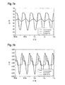
- FIG. 7 a shows a graphic representation of an electric voltage u(t) determined in the calibration plane with the method according to the invention using the (corrected) calibration parameters e 00,r , e 01,r , e 10,r , e 11,r and using the (uncorrected) calibration parameters e 00 , e 01 , e 10 , e 11 for an input first RF signal; and
- FIG. 7 b shows a graphic representation of an electric current i(t) determined in the calibration plane with the method according to the invention using the (corrected) calibration parameters e 00,r , e 01,r , e 10,r , e 11,r and using the (uncorrected) calibration parameters e 00 , e 01 , e 10 , e 11 for an input first RF signal.
- FIGS. 1-7 of the drawings in which like numerals refer to like features of the invention.
- the invention is based on the knowledge that the method described in the document WO2013/143650 A1 only provides exact results if the two measuring inputs of the time domain measuring device have reflection-free terminations.
- the calibration apparatus had already been calibrated previously to the measuring ports used and will thus behave ideally.
- the calibration parameters which are necessary during the measuring step in order to obtain an exact measurement depend on the reflection coefficients ⁇ 3 and ⁇ 4 at the measuring inputs of the time domain measuring device.
- any time domain measuring devices can be connected to the measuring outputs of the directional coupler for the measurement in the time domain, since the calibration parameters are determined in relation to the reflection coefficients at the measuring inputs of the time domain measuring device.
- the reflection coefficients ⁇ 3 and ⁇ 4 of the measuring inputs of the time domain measuring device are known when determining the voltage and/or the current in the measuring step, or can be determined through separate measurement, so that the frequency-dependent e 00,r ( ⁇ 3 , ⁇ 4 ), e 01,r ( ⁇ 3 , ⁇ 4 ), e 10,r ( ⁇ 3 , ⁇ 4 ), e 11,r ( ⁇ 3 , ⁇ 4 ) can be used as calibration parameters.
- the determination of the wave quantities a 2 and b 2 in the calibration plane from the wave quantities b 3 and b 4 in the measuring planes can be carried out particularly quickly and reliably if the calibration parameters e 00,r , e 01,r , e 10,r , e 11,r link the wave quantity b 3 running in at the second measuring port S 3 and the wave quantity b 4 running in at the third measuring port S 4 with the wave quantities b 2 , a 2 running in and out in the calibration plane S 2 as follows:
- the four-port whose scattering parameters S xy are determined has the following four ports:
- This four-port is present in unchanged form during the calibration step and during the measuring step (or changes in the input cable to the directional coupler have no effect, since the terms dependent on the input cable are eliminated during the determination of e xy ), so that the determined scattering parameters S xy of the four-port determined during the calibration are still correct during the measuring step and can be used for determination of the corrected error matrix E r .
- the scattering parameters of an n-port are by definition independent of the external wiring.
- the error matrix E r the terms of which are needed during the measurement, depends on the reflection coefficients at the measuring ports of the time domain measuring device, but not on the properties of the input cable between the signal generator and the signal input of the directional coupler.
- a corrected error matrix E r can be determined from the scattering parameters S xy using the known reflection coefficients ⁇ 3 , ⁇ 4 of the time domain measuring device, as follows:
- the scattering parameters S xy are determined by measuring the values b 1 /a 1 , b 3 /a 3 , b 4 /a 4 , b 3 /a 1 or b 1 /a 3 , b 4 /a 1 or b 1 /a 4 , b 4 /a 3 or b 3 /a 4 at the measuring ports S 1 , S 3 , S 4 of the calibration device, where one or more measuring standards such as Match M, Open O and/or Short S with the known reflection coefficients ⁇ M , ⁇ O , ⁇ S are connected as devices under test in the calibration plane S 2 , where a 1 , a 3 , a 4 are the wave quantities running in at the respective measuring ports S 1 , S 3 , S 4 and b 1 , b 3 , b 4 are the wave quantities running out at the respective measuring ports S 1 , S 3 , S 4 .
- one or more measuring standards such as Match M, Open O and/or Short S with the known
- S 11 i 00
- S 21 i 10
- S 12 i 01
- S 22 i 11
- ⁇ S 33 S ⁇ 33 - ⁇ DUT ⁇ S 23 1 - ⁇ DUT ⁇ i 11 ⁇ S 32 .
- ⁇ S 44 S ⁇ 44 - ⁇ DUT ⁇ S 24 1 - ⁇ DUT ⁇ i 11 ⁇ S 42 , where
- ⁇ O , ⁇ S , ⁇ M are the known reflection coefficients of the calibration standards Open, Short and Match, and are the b x /a y measurable at the measuring ports S 1 , S 3 , S 4 with connected calibration standard K.
- a particularly simple measuring setup using economical electronic components is achieved in that the signal values v 3 (t) and v 4 (t) are in each case an electric voltage.
- a particularly simple and functionally reliable measuring setup is achieved in that an oscilloscope is used as time domain measuring device, for example a digital oscilloscope, which can be used for time- and value-range quantisation of the signal.
- an oscilloscope is used as time domain measuring device, for example a digital oscilloscope, which can be used for time- and value-range quantisation of the signal.
- the first mathematical operation is an FFT (Fast Fourier Transform) and the second mathematical operation an inverse FFT (IFFT—Inverse Fast Fourier Transform).
- FFT Fast Fourier Transform
- IFFT inverse Fast Fourier Transform
- the wave quantities b 3 and b 4 are preferably determined from the voltages V 3 and V 4 as follows:
- the absolute wave quantities a 2 , b 2 in the calibration plane are determined from the wave quantities b 3 , b 4 , with the aid of the calibration parameters (e 00,r ( ⁇ 3 , ⁇ 4 ), e 01,r ( ⁇ 3 , ⁇ 4 ), e 10,r ( ⁇ 3 , ⁇ 4 ), e 11,r ( ⁇ 3 , ⁇ 4 )), through corresponding resolution of the equation system
- V 2 Z 1 ⁇ ( a 2 + b 2 )
- I 2 1 Z 1 ⁇ ⁇ ( a 2 - b 2 )
- Z 1 designates the system impedance in the calibration plane.
- VNA vectorial network analyser
- NWA vectorial NWA
- the voltage u(t) and/or the current i(t) in the calibration plane can then be determined in the measuring step in that the first measuring output of the directional coupler and the second measuring output of the directional coupler are isolated from the calibration device and connected with the measuring inputs of the time domain measuring device, while the first RF signal is fed via the signal input of the directional coupler.
- FIG. 1 An arrangement for carrying out the calibration step of the method according to the invention is represented schematically in FIG. 1 .
- This arrangement features a directional coupler 18 with a signal input 19 which is connected via an input cable 10 with a first measuring port S 1 28 of a calibration device 26 (vectorial network analyser VNA).
- a calibration plane 14 is connected with the signal output of the directional coupler.
- the calibration plane 14 is designed such that a device under test (DUT) 16 can be connected electrically to the calibration plane 14 .
- This DUT 16 is for example a calibration standard, an electronic circuit which is to be tested or an electronic component.
- a component of a first RF signal, which runs within the directional coupler 18 from the signal input 19 in the direction of the calibration plane 14 , and a component of a second RF signal, which runs within the directional coupler 18 from the calibration plane 14 in the direction of the signal input 19 , are decoupled by means of the directional coupler 18 with two measuring outputs 20 , 22 .
- the first signal output 20 of the directional coupler 18 is connected with a second measuring port S 3 30 of the VNA, and the second signal output 22 of the directional coupler 18 is connected with a third measuring port S 4 32 of the VNA.
- Suitable for use as a directional coupler 18 is any component which possesses directionality, i.e., which makes it possible to distinguish the component of the first RF signal and the component of the second RF signal.
- a signal is input via the first measuring port 28 .
- the calibration plane 14 which is connected with the signal output of the coupler 18 , is represented by the port S 2 of the four-port S with the ports S 1 to S 4 which is to be measured, since the device under test 16 which is to be measured is connected at this point. For this reason the calibration plane is also referred to as port S 2 in the following description.
- the four-port S which is to be measured which in the present case is used both in the calibration step and in the measuring step, thus substantially comprises the directional coupler 18 together with input cables.
- FIG. 4 a The four-port between the three measuring ports S 1 , S 3 and S 4 ( 28 , 30 , 32 ) of the VNA and the calibration plane S 2 14 is represented schematically in FIG. 4 a .
- This four-port can be broken down into two (error) two-ports, which are represented schematically in FIGS. 4 b and 4 c and as signal flow diagrams in FIGS. 3 a and 3 b and which can be described through the two error matrices I and E.
- error coefficients ( i 00 i 01 i 10 i 11 ) , also referred to as error coefficients, is located between the measuring port S 1 28 of the NWA and the calibration plane S 2 14 ; the two-port with the error coefficients
- the four entries e xy of the (uncorrected) error matrix E are to be determined, which express the relationship between the wave quantities a 2 and b 2 in the calibration plane and the decoupled wave quantities b 3 and b 4 decoupled through the directional coupler 18 for the four-port S which is terminated in a reflection-free manner at the measuring ports S 3 and S 4 . Consequently, the VNA 26 is terminated in a reflection-free manner at its measuring ports.
- the entries e xy the (corrected) calibration parameters
- the calibration is extended in the following. It should firstly be noted that the error matrix E obtained through the mathematical operation of the four-port-two-port reduction does not describe a reciprocal two-port, i.e. e 10 ⁇ e 01 . In contrast, the error matrix I describes the relationship between the measuring port S 1 of the VNA 26 and the calibration plane 14 , S 2 and can thus be assumed to be reciprocal.
- the decision regarding the correct sign in equation (4) is equivalent to the correct determination of the phase of i 10 from two possibilities. To do this, one proceeds as follows: the phase at a frequency point must be known with adequate precision in order to decide on the sign. This can for example be done through an estimation of the electric length of the setup between the measuring port S 1 of the VNA 26 and the calibration plane S 2 , 14 . It is also assumed that the phase changes by less than 90° between two adjacent frequency points. The correct phase of i 10 can thus also be determined for all frequency points.
- the following relationships for b 2 can be derived from the graphs in FIGS. 3 a and 3 b :
- a 1 b 3 S ⁇ 31 - 1 , so that e 10 can be determined individually and, from this, using (2), also e 01 .
- a 2 b 4 - e 00 ⁇ b 3 e 01 ( 7 ) derived from the signal flow graphs according to FIG. 3 , after determining the four coefficients of the error matrix E from measured b 3 and b 4 , the absolute wave quantities a 2 and b 2 in the calibration plane 14 can now be determined for a time domain measuring device with reflection-free termination.
- time domain measuring devices 34 such as oscilloscopes are generally not terminated in a perfectly reflection-free manner. Rather, they can display reflection coefficients ⁇ 3 ⁇ 0 and/or ⁇ 4 ⁇ 0 at their measuring inputs 36 , 38 , at which the signal components 72 , 74 run in in the measuring step shown in FIG. 2 .
- the entries e xy of the (uncorrected) error matrix E described above were determined on the assumption of a reflection-free termination of the time domain measuring device 34 , so that no exact voltages and/or currents in the calibration plane can be determined if a time domain measuring device 34 with ⁇ 3 ⁇ 0 and/or ⁇ 4 ⁇ 0 is used.
- This example involves the four-port as shown in FIG. 3 a , described through its scattering matrix S. If this four-port represents the directional coupler 18 together with input cables, then the signal input 19 of the directional coupler 18 is connected with the measuring port S 1 28 of the network analyser 26 during the calibration, and during the measurement is for example connected with a signal source 24 .
- the measuring outputs 20 and 22 of the four-port/directional coupler 18 are connected with the measuring ports S 3 and S 4 of the VNA 26 during the calibration and are connected with the measuring inputs 36 , 38 of the time domain measuring device 34 during the measurement.
- the calibration standards are connected with port S 2 of the four-port, the calibration plane 14 , during the calibration and the device under test 16 which is to be measured is connected with this during the measurement.
- S 44 and S 34 of the four-port can also be derived if, analogously, an input via the port S 4 is considered:
- the measuring step for determining the electric voltage u(t) and the electric current i(t) of the RF signal in the calibration plane ( 14 ) in the method according to the invention is described in the following.
- the use of the calibration parameters e xy,r is explained in the following. It should be emphasised that only the marked part of the setup (enclosed in a broken line) needs to remain unchanged in comparison with the calibration. This substantially involves the directional coupler 18 as far as the calibration plane 14 as well as the cables which connect the directional coupler 18 with the time domain measuring device 34 . In contrast, changes—also in the characteristic impedance—to the other elements, for example the source and the load, have no influence on the measurement. It is assumed that the setup between the calibration plane 14 and the measuring inputs 36 , 38 and the measuring outputs 20 , 22 of the directional coupler 18 does not change in comparison with the calibration according to FIG. 1 if the obtained calibration coefficients are to remain valid. In contrast, changes to the signal source 24 b and its input cable 10 b to the directional coupler have no influence on the calibration.
- V 3 ⁇ ( l ⁇ ⁇ ⁇ ⁇ f ) ⁇ FFT ⁇ ⁇ v 3 ⁇ ( k ⁇ ⁇ ⁇ ⁇ t ) ⁇ ( 17 ) ⁇
- V 4 ⁇ ( l ⁇ ⁇ ⁇ ⁇ f ) ⁇ FFT ⁇ ⁇ v 4 ⁇ ( k ⁇ ⁇ ⁇ ⁇ t ) ⁇ ⁇ ⁇
- ⁇ ⁇ k 0 , 1 , ... ⁇ , N - 1 ⁇ ⁇
- ⁇ ⁇ l 0 , 1 , ... ⁇ , N - 1 2 .
- b 3 V 3 ( 1 + ⁇ 3 ) ⁇ Z D ( 19 )
- b 4 V 4 ( 1 + ⁇ 4 ) ⁇ Z D , ( 20 )
- the absolute wave quantities a 2 , b 2 in the calibration plane are determined from these wave quantities with the aid of the calibration parameters (e 00,r ( ⁇ 3 , ⁇ 4 ), e 01,r ( ⁇ 3 , ⁇ 4 ), e 10,r ( ⁇ 3 , ⁇ 4 ), e 11,r ( ⁇ 3 , ⁇ 4 )) using the equations (3), (5) and (7), where e xy is in each case replaced with e xy,r ( ⁇ 3 , ⁇ 4 ), and the voltage V 2 and the current I 2 in the calibration plane are derived from these:
- V 2 Z 1 ⁇ ( a 2 + b 2 ) ( 21 )
- I 2 1 Z 1 ⁇ ⁇ ( a 2 - b 2 ) , ( 22 )
- Z 1 designates the system impedance in the calibration plane. This is the impedance on which the statement of the reflection coefficients ⁇ O,S,M of the calibration standards was based during the calibration. This need not be the physical line impedance in the calibration plane 14 . Any choice of Z 1 , which must, however, be consistent between calibration and measurement, has no influence on the measurement result.
- the time-discrete representation of the voltage u(t) and of the current i(t) in the calibration plane can be obtained from V 2 (f) and I 2 (f) with the aid of the inverse FFT (IFFT):
- FIGS. 7 a and 7 b show the voltage u(t) and the current i(t) in the calibration plane. It can be seen that where the calibration parameters e xy which are not corrected by the mismatch are used, as shown in FIG. 6 a , neither the amplitude nor the form of the curves are correctly reproduced. In contrast, both the voltage and the current are consistent with the reference determined through simulation if the corrected calibration parameters e xy,r corrected by means of the method according to the invention are used (see FIG. 6 b ).
- a time domain measuring device with measuring inputs with reflection-free termination need not necessarily be used, and that reflection coefficients ⁇ 3 ⁇ 0 and/or ⁇ 4 ⁇ 0 can be corrected.
Landscapes
- Physics & Mathematics (AREA)
- General Physics & Mathematics (AREA)
- Measurement Of Resistance Or Impedance (AREA)
Applications Claiming Priority (4)
| Application Number | Priority Date | Filing Date | Title |
|---|---|---|---|
| DE102014001585 | 2014-02-06 | ||
| DE102014001585.8 | 2014-02-06 | ||
| DE102014001585.8A DE102014001585A1 (de) | 2014-02-06 | 2014-02-06 | Zeitbereichsmessverfahren mit Kalibrierung im Frequenzbereich |
| PCT/EP2014/003424 WO2015117634A1 (de) | 2014-02-06 | 2014-12-18 | Zeitbereichsmessverfahren mit kalibrierung im frequenzbereich |
Publications (2)
| Publication Number | Publication Date |
|---|---|
| US20170074911A1 US20170074911A1 (en) | 2017-03-16 |
| US10191092B2 true US10191092B2 (en) | 2019-01-29 |
Family
ID=52130203
Family Applications (1)
| Application Number | Title | Priority Date | Filing Date |
|---|---|---|---|
| US15/116,428 Active 2035-04-09 US10191092B2 (en) | 2014-02-06 | 2014-12-18 | Time domain measuring method with calibration in the frequency range |
Country Status (9)
| Country | Link |
|---|---|
| US (1) | US10191092B2 (ko) |
| EP (1) | EP3102961B1 (ko) |
| JP (1) | JP6360901B2 (ko) |
| KR (1) | KR102090014B1 (ko) |
| CN (1) | CN105980878B (ko) |
| CA (1) | CA2928579C (ko) |
| DE (1) | DE102014001585A1 (ko) |
| TW (1) | TWI631357B (ko) |
| WO (1) | WO2015117634A1 (ko) |
Families Citing this family (6)
| Publication number | Priority date | Publication date | Assignee | Title |
|---|---|---|---|---|
| US20170045603A1 (en) * | 2015-08-14 | 2017-02-16 | Tektronix, Inc. | Synchronization of unstable signal sources for use in a phase stable instrument |
| KR102013838B1 (ko) * | 2018-05-03 | 2019-08-26 | 주식회사 이노와이어리스 | 전압 정재파비 측정 장치 및 그 제어 방법 |
| CN112924761B (zh) * | 2020-12-28 | 2023-05-26 | 北京无线电计量测试研究所 | 一种用于脉冲波形不确定度评定的方法和控制器 |
| CN113433502B (zh) * | 2021-07-28 | 2022-09-06 | 武汉市华英电力科技有限公司 | 一种基于波形仿真的电容电感测试仪校准方法和装置 |
| EP4145149A1 (en) * | 2021-09-07 | 2023-03-08 | TMY Technology Inc. | Broadband measurement system and measurement method for broadband property |
| DE102021214761B3 (de) | 2021-12-21 | 2023-05-25 | Volkswagen Aktiengesellschaft | Verfahren und Messanordnung zum Bestimmen von elektrischen Größen für ein Verhaltensmodell einer elektrischen oder elektronischen Störquelle |
Citations (13)
| Publication number | Priority date | Publication date | Assignee | Title |
|---|---|---|---|---|
| JPH07151803A (ja) | 1993-08-30 | 1995-06-16 | Rohde & Schwarz Gmbh & Co Kg | ネットワークアナライザー |
| JP2001272428A (ja) | 1999-02-05 | 2001-10-05 | Advantest Corp | ネットワークアナライザ、ネットワーク分析方法およびネットワーク分析プログラムを記録した記録媒体 |
| WO2003048791A2 (en) | 2001-11-29 | 2003-06-12 | University College Cardiff Consultants Ltd. | High frequency circuit analyser |
| JP2007285890A (ja) | 2006-04-17 | 2007-11-01 | Agilent Technol Inc | ネットワークアナライザの再校正方法、および、ネットワークアナライザ |
| WO2008016699A2 (en) | 2006-08-02 | 2008-02-07 | Lecroy Corporation | Virtual probing |
| US20080048674A1 (en) | 2006-08-23 | 2008-02-28 | Kan Tan | Signal analysis system and calibration method for processing acquires signal samples with an arbitrary load |
| CN100471187C (zh) | 2001-01-22 | 2009-03-18 | 皇家菲利浦电子有限公司 | 为单载波信号提供频域同步的系统和方法 |
| JP2009068932A (ja) | 2007-09-12 | 2009-04-02 | Campus Create Co Ltd | 線形マルチポートのシステムパラメータの測定方法及び装置、ベクトルネットワークアナライザを用いた測定方法並びにプログラム |
| CN101441232A (zh) | 2008-12-25 | 2009-05-27 | 中南大学 | 一种时基频率实时校准测频方法及其装置 |
| US20120109566A1 (en) * | 2010-11-02 | 2012-05-03 | Ate Systems, Inc. | Method and apparatus for calibrating a test system for measuring a device under test |
| WO2013048791A1 (en) | 2011-10-01 | 2013-04-04 | Oracle International Corporation | Expense entry for mobile expense solutions |
| WO2013143650A1 (de) | 2012-03-28 | 2013-10-03 | Rosenberger Hochfrequenztechnik Gmbh & Co. Kg | Zeitbereichsmessverfahren mit kalibrierung im frequenzbereich |
| TW201403082A (zh) | 2012-03-27 | 2014-01-16 | Rosenberger Hochfrequenztech | 向量網路分析器及其測定電子待測物件控制參數之方法 |
Family Cites Families (2)
| Publication number | Priority date | Publication date | Assignee | Title |
|---|---|---|---|---|
| JP4462979B2 (ja) * | 2004-03-26 | 2010-05-12 | 株式会社アドバンテスト | ネットワークアナライザ、伝送トラッキング測定方法、ネットワーク解析方法、プログラムおよび記録媒体 |
| JP2009058348A (ja) * | 2007-08-31 | 2009-03-19 | Campus Create Co Ltd | ベクトルネットワークアナライザを用いた測定方法及びその校正方法並びにプログラム |
-
2014
- 2014-02-06 DE DE102014001585.8A patent/DE102014001585A1/de not_active Withdrawn
- 2014-12-18 WO PCT/EP2014/003424 patent/WO2015117634A1/de active Application Filing
- 2014-12-18 KR KR1020167013332A patent/KR102090014B1/ko active IP Right Grant
- 2014-12-18 US US15/116,428 patent/US10191092B2/en active Active
- 2014-12-18 EP EP14815243.2A patent/EP3102961B1/de active Active
- 2014-12-18 CA CA2928579A patent/CA2928579C/en active Active
- 2014-12-18 JP JP2016549762A patent/JP6360901B2/ja active Active
- 2014-12-18 CN CN201480075121.0A patent/CN105980878B/zh active Active
-
2015
- 2015-01-09 TW TW104100800A patent/TWI631357B/zh not_active IP Right Cessation
Patent Citations (14)
| Publication number | Priority date | Publication date | Assignee | Title |
|---|---|---|---|---|
| JPH07151803A (ja) | 1993-08-30 | 1995-06-16 | Rohde & Schwarz Gmbh & Co Kg | ネットワークアナライザー |
| JP2001272428A (ja) | 1999-02-05 | 2001-10-05 | Advantest Corp | ネットワークアナライザ、ネットワーク分析方法およびネットワーク分析プログラムを記録した記録媒体 |
| CN100471187C (zh) | 2001-01-22 | 2009-03-18 | 皇家菲利浦电子有限公司 | 为单载波信号提供频域同步的系统和方法 |
| WO2003048791A2 (en) | 2001-11-29 | 2003-06-12 | University College Cardiff Consultants Ltd. | High frequency circuit analyser |
| JP2007285890A (ja) | 2006-04-17 | 2007-11-01 | Agilent Technol Inc | ネットワークアナライザの再校正方法、および、ネットワークアナライザ |
| WO2008016699A2 (en) | 2006-08-02 | 2008-02-07 | Lecroy Corporation | Virtual probing |
| US20080048674A1 (en) | 2006-08-23 | 2008-02-28 | Kan Tan | Signal analysis system and calibration method for processing acquires signal samples with an arbitrary load |
| JP2009068932A (ja) | 2007-09-12 | 2009-04-02 | Campus Create Co Ltd | 線形マルチポートのシステムパラメータの測定方法及び装置、ベクトルネットワークアナライザを用いた測定方法並びにプログラム |
| CN101441232A (zh) | 2008-12-25 | 2009-05-27 | 中南大学 | 一种时基频率实时校准测频方法及其装置 |
| US20120109566A1 (en) * | 2010-11-02 | 2012-05-03 | Ate Systems, Inc. | Method and apparatus for calibrating a test system for measuring a device under test |
| WO2013048791A1 (en) | 2011-10-01 | 2013-04-04 | Oracle International Corporation | Expense entry for mobile expense solutions |
| TW201403082A (zh) | 2012-03-27 | 2014-01-16 | Rosenberger Hochfrequenztech | 向量網路分析器及其測定電子待測物件控制參數之方法 |
| WO2013143650A1 (de) | 2012-03-28 | 2013-10-03 | Rosenberger Hochfrequenztechnik Gmbh & Co. Kg | Zeitbereichsmessverfahren mit kalibrierung im frequenzbereich |
| US9823281B2 (en) * | 2012-03-28 | 2017-11-21 | Rosenberger Hochfrequenztechnik Gmbh & Co. Kg | Time frame measuring method with calibration in the frequency range |
Non-Patent Citations (6)
| Title |
|---|
| Arkadiuz Lewandowski et al.: "Covariance-Based Vector-Network-Analyzer Uncertainty Analysis for Time and Frequency-Domain Measurements", IEEE Transactions on Microwave Theory and Techniques, vol. 58, No. 7, Jul. 1, 2010, pp. 1877-1886. |
| Clement T.S. et al.: "Calibration of Sampling Oscilloscopes with High-Speed Photodiodes", IEEE Transaction on Microwave Theory and Techniques, vol. 54, No. 8, Aug. 1, 2006, pp. 3173-3181. |
| Gillon R. et al.: The application of large-signal calibration techniques yields unprecedented insight during TLP and ESD testing. In: EOS/ESD Symposium, 2009, S. 1-7. ISBN 1-58537-176-9. |
| Root, D. et al.: X-Parameter: The new paradigm for the description of nonlinear RF and microwave devices. In: tm-Technisches Messen, 2010, No. 7-8, vol. 77. |
| Scott, J.B. et al.: A new instrument architecture for millimeter-wave time-domain signal analysis. In: ARFTG 63rd Conference, 2004, S. 47-52. ISBN 0-7803-8371-0. |
| Siart, U.: Calibration of network analyzers. As of Jan. 4, 2012, Version 1.51. URL: http://www.siart.de/lehre/nwa.pdf [clicked on May 9, 2014]. |
Also Published As
| Publication number | Publication date |
|---|---|
| JP2017505441A (ja) | 2017-02-16 |
| CN105980878B (zh) | 2019-01-18 |
| TW201531728A (zh) | 2015-08-16 |
| KR20160118209A (ko) | 2016-10-11 |
| TWI631357B (zh) | 2018-08-01 |
| US20170074911A1 (en) | 2017-03-16 |
| CA2928579C (en) | 2020-04-28 |
| EP3102961B1 (de) | 2017-06-07 |
| DE102014001585A1 (de) | 2015-08-06 |
| KR102090014B1 (ko) | 2020-05-28 |
| WO2015117634A1 (de) | 2015-08-13 |
| JP6360901B2 (ja) | 2018-07-18 |
| EP3102961A1 (de) | 2016-12-14 |
| CN105980878A (zh) | 2016-09-28 |
| CA2928579A1 (en) | 2015-08-13 |
Similar Documents
| Publication | Publication Date | Title |
|---|---|---|
| US10191092B2 (en) | Time domain measuring method with calibration in the frequency range | |
| KR102054874B1 (ko) | 시험 장치를 교정하기 위한 방법 | |
| US9823281B2 (en) | Time frame measuring method with calibration in the frequency range | |
| US7038468B2 (en) | Method and a test setup for measuring large-signal S-parameters that include the coefficients relating to the conjugate of the incident waves | |
| CN106405462B (zh) | 在片散射参数的溯源及不确定度评估方法 | |
| JP2007519892A (ja) | 複数のテストフィクスチャを使用するときのテストシステム校正の補正および装置測定値の変換 | |
| Zietz et al. | A general calibration procedure for measuring RF voltages and currents applied to the EMC analysis of automotive high-voltage power networks | |
| EP3574331B1 (en) | An interferometric iq-mixer/dac solution for active, high speed vector network analyser impedance renormalization | |
| US8000916B2 (en) | System and method for evaluating high frequency time domain in embedded device probing | |
| US10509064B2 (en) | Impedance measurement through waveform monitoring | |
| US7268530B1 (en) | Method to measure the mutual phase relationship of a set of spectral components generated by a signal generator | |
| Ferrero et al. | Uncertainty in multiport S-parameters measurements | |
| JP2017106921A (ja) | 信号測定方法 | |
| Cho et al. | Uncertainty analysis for characterization of a commercial real-time oscilloscope using a calibrated pulse standard | |
| Fezai et al. | Characterization of reflection and attenuation parameters of device under test by vna | |
| Sampath et al. | Signal integrity validation of de-embedding techniques using accurate transfer functions | |
| CN115248364A (zh) | 高频元件测试装置及其测试方法 |
Legal Events
| Date | Code | Title | Description |
|---|---|---|---|
| AS | Assignment |
Owner name: ROSENBERGER HOCHFREQUENZTECHNIK GMBH & CO. KG, GER Free format text: ASSIGNMENT OF ASSIGNORS INTEREST;ASSIGNOR:ZIETZ, CHRISTIAN;REEL/FRAME:039414/0884 Effective date: 20160425 |
|
| STCF | Information on status: patent grant |
Free format text: PATENTED CASE |
|
| CC | Certificate of correction | ||
| MAFP | Maintenance fee payment |
Free format text: PAYMENT OF MAINTENANCE FEE, 4TH YEAR, LARGE ENTITY (ORIGINAL EVENT CODE: M1551); ENTITY STATUS OF PATENT OWNER: LARGE ENTITY Year of fee payment: 4 |