US10041997B2 - System and method for fault isolation by emission spectra analysis - Google Patents
System and method for fault isolation by emission spectra analysis Download PDFInfo
- Publication number
- US10041997B2 US10041997B2 US14/657,605 US201514657605A US10041997B2 US 10041997 B2 US10041997 B2 US 10041997B2 US 201514657605 A US201514657605 A US 201514657605A US 10041997 B2 US10041997 B2 US 10041997B2
- Authority
- US
- United States
- Prior art keywords
- diffraction spectrum
- classifying
- integrated circuit
- image
- dut
- Prior art date
- Legal status (The legal status is an assumption and is not a legal conclusion. Google has not performed a legal analysis and makes no representation as to the accuracy of the status listed.)
- Active, expires
Links
- 238000000034 method Methods 0.000 title claims abstract description 47
- 238000004458 analytical method Methods 0.000 title description 12
- 238000000295 emission spectrum Methods 0.000 title description 4
- 238000002955 isolation Methods 0.000 title 1
- 238000012360 testing method Methods 0.000 claims abstract description 25
- 238000001228 spectrum Methods 0.000 claims description 72
- 230000003287 optical effect Effects 0.000 abstract description 46
- 230000003068 static effect Effects 0.000 abstract description 7
- 238000003384 imaging method Methods 0.000 abstract description 4
- XUIMIQQOPSSXEZ-UHFFFAOYSA-N Silicon Chemical compound [Si] XUIMIQQOPSSXEZ-UHFFFAOYSA-N 0.000 description 9
- 229910052710 silicon Inorganic materials 0.000 description 9
- 239000010703 silicon Substances 0.000 description 9
- 238000000386 microscopy Methods 0.000 description 8
- 230000003595 spectral effect Effects 0.000 description 8
- 239000000523 sample Substances 0.000 description 7
- 230000004044 response Effects 0.000 description 6
- 238000013507 mapping Methods 0.000 description 5
- 230000005540 biological transmission Effects 0.000 description 4
- 230000008859 change Effects 0.000 description 4
- 238000001514 detection method Methods 0.000 description 4
- 238000005516 engineering process Methods 0.000 description 4
- 239000000835 fiber Substances 0.000 description 4
- 238000005286 illumination Methods 0.000 description 4
- 230000002123 temporal effect Effects 0.000 description 4
- 230000009286 beneficial effect Effects 0.000 description 3
- 239000004020 conductor Substances 0.000 description 3
- 238000000926 separation method Methods 0.000 description 3
- 239000013598 vector Substances 0.000 description 3
- 230000007547 defect Effects 0.000 description 2
- 238000013461 design Methods 0.000 description 2
- 230000009977 dual effect Effects 0.000 description 2
- 230000000694 effects Effects 0.000 description 2
- 230000004807 localization Effects 0.000 description 2
- 238000005259 measurement Methods 0.000 description 2
- 239000002184 metal Substances 0.000 description 2
- 238000004377 microelectronic Methods 0.000 description 2
- 230000008569 process Effects 0.000 description 2
- 239000007787 solid Substances 0.000 description 2
- 229910000530 Gallium indium arsenide Inorganic materials 0.000 description 1
- 229910000661 Mercury cadmium telluride Inorganic materials 0.000 description 1
- 238000010521 absorption reaction Methods 0.000 description 1
- 230000008901 benefit Effects 0.000 description 1
- 230000000903 blocking effect Effects 0.000 description 1
- 238000006243 chemical reaction Methods 0.000 description 1
- 238000007405 data analysis Methods 0.000 description 1
- 238000013480 data collection Methods 0.000 description 1
- 230000002950 deficient Effects 0.000 description 1
- 230000001419 dependent effect Effects 0.000 description 1
- 238000010586 diagram Methods 0.000 description 1
- 239000006185 dispersion Substances 0.000 description 1
- 238000005401 electroluminescence Methods 0.000 description 1
- 230000002708 enhancing effect Effects 0.000 description 1
- 238000011156 evaluation Methods 0.000 description 1
- 238000007654 immersion Methods 0.000 description 1
- 238000007689 inspection Methods 0.000 description 1
- 239000004973 liquid crystal related substance Substances 0.000 description 1
- 239000000463 material Substances 0.000 description 1
- 238000000691 measurement method Methods 0.000 description 1
- 230000007246 mechanism Effects 0.000 description 1
- 238000012986 modification Methods 0.000 description 1
- 230000004048 modification Effects 0.000 description 1
- 238000012544 monitoring process Methods 0.000 description 1
- 230000005693 optoelectronics Effects 0.000 description 1
- 230000010363 phase shift Effects 0.000 description 1
- 230000010287 polarization Effects 0.000 description 1
- 238000012827 research and development Methods 0.000 description 1
- 238000012552 review Methods 0.000 description 1
- 238000005070 sampling Methods 0.000 description 1
- 229920006395 saturated elastomer Polymers 0.000 description 1
- 230000001360 synchronised effect Effects 0.000 description 1
Images


Classifications
-
- G—PHYSICS
- G01—MEASURING; TESTING
- G01R—MEASURING ELECTRIC VARIABLES; MEASURING MAGNETIC VARIABLES
- G01R31/00—Arrangements for testing electric properties; Arrangements for locating electric faults; Arrangements for electrical testing characterised by what is being tested not provided for elsewhere
- G01R31/28—Testing of electronic circuits, e.g. by signal tracer
- G01R31/302—Contactless testing
- G01R31/308—Contactless testing using non-ionising electromagnetic radiation, e.g. optical radiation
- G01R31/311—Contactless testing using non-ionising electromagnetic radiation, e.g. optical radiation of integrated circuits
-
- G—PHYSICS
- G01—MEASURING; TESTING
- G01N—INVESTIGATING OR ANALYSING MATERIALS BY DETERMINING THEIR CHEMICAL OR PHYSICAL PROPERTIES
- G01N21/00—Investigating or analysing materials by the use of optical means, i.e. using sub-millimetre waves, infrared, visible or ultraviolet light
- G01N21/84—Systems specially adapted for particular applications
- G01N21/88—Investigating the presence of flaws or contamination
- G01N21/95—Investigating the presence of flaws or contamination characterised by the material or shape of the object to be examined
- G01N21/9501—Semiconductor wafers
- G01N21/9505—Wafer internal defects, e.g. microcracks
-
- G—PHYSICS
- G01—MEASURING; TESTING
- G01N—INVESTIGATING OR ANALYSING MATERIALS BY DETERMINING THEIR CHEMICAL OR PHYSICAL PROPERTIES
- G01N21/00—Investigating or analysing materials by the use of optical means, i.e. using sub-millimetre waves, infrared, visible or ultraviolet light
- G01N21/84—Systems specially adapted for particular applications
- G01N21/88—Investigating the presence of flaws or contamination
- G01N21/95—Investigating the presence of flaws or contamination characterised by the material or shape of the object to be examined
- G01N21/956—Inspecting patterns on the surface of objects
Definitions
- the present invention relates to an apparatus and method for optically probing integrated circuits by switching of an electronic elements in the device under test (DUT).
- the invention relates to identifying, localizing, and classifying malfunctioning elements.
- LVP Laser Voltage Probe
- a commercially available testing platform such as, e.g., Automated Testing Equipment, also known as an Automated Testing and Evaluation (ATE) tester, is used to generate test patterns (also referred to as test vectors) to be applied to the IC device under test (DUT).
- test patterns also referred to as test vectors
- ATE Automated Testing and Evaluation
- Various systems and methods can then be used to test the response of the DUT to the test vectors.
- One such method is generally referred to as emission microscopy. Emission microscopy collects the photon emission generated inside an integrated circuit.
- Emission microscopy includes static emission microscopy, when photons are emitted when the signal applied to the DUT is static, and dynamic emission microscopy, when the signal applied to the DUT causes devices inside the DUT to be active, i.e., switch.
- emission microscopy no illumination is used during the actual testing period.
- other method utilize illumination for the testing, such as, e.g., laser voltage probing (LVP).
- LVP laser voltage probing
- the DUT is illuminated by the laser and the light reflected from the DUT is collected by the probing system. As the laser beam strikes the DUT, the laser beam is modulated by the response of various elements (switching transistors) of the DUT to the test vectors.
- Emission microscopy system utilizes most of the elements of laser-based systems, since even in emission microscope illumination such as laser illumination is used for navigation and imaging of the DUT. Accordingly, a short description of a laser-based microscope is provided below, with the understanding that much of the description is equally applicable to emission system.
- FIG. 1 is a general schematic depicting major components of an optical probing system architecture, 100 , according to the prior art.
- dashed arrows represent optical path
- solid arrows represent electronic signal path.
- the optical paths represented by curved lines are generally made using fiber optic cables.
- Probe system 100 comprises a laser source which, in this particular example, is a dual laser source, DLS 110 , an optical bench 112 , and data acquisition and analysis apparatus 114 .
- the optical bench 112 includes provisions for mounting the DUT 160 .
- a conventional ATE tester 140 provides stimulus signals and receives response signals 142 to/from the DUT 160 and may provide trigger and clock signals, 144 , to the time-base board 155 .
- the signal from the tester is generally transferred to the DUT via test boards, DUT board (adapter plate) and various cables and interfaces that connect all of these components.
- the ATE and the optical probing systems are produced and sold by different and unrelated companies.
- the reference to the description of embodiments of the inventive system relate only to the optical probing system and not to the ATE. That is, the ATE is not part of the optical probing system 100 .
- the time-base board 155 synchronizes the signal acquisition with the DUT stimulus and the laser pulses.
- Workstation 170 controls as well as receives, processes, and displays data from the signal acquisition board 150 , time-base board 155 , and the optical bench 112 .
- Dual laser source 110 consists of two lasers: a pulsed mode-locked laser, MLL 104 , source that is used to generate 10-35 ps wide pulses, and a continuous-wave laser source, CWL 106 , that can be externally gated to generate approximately 1 us wide pulses.
- MLL 104 pulsed mode-locked laser
- CWL 106 continuous-wave laser source
- the MLL 104 source runs at a fixed frequency, typically 100 MHz, and must be synchronized with the stimulus 142 provided to the DUT 160 , via a phase-locked loop (PLL) on the time-base board 155 , and the trigger and clock signals 144 provided by the ATE tester.
- the output of the DLS 110 is transmitted to the optical bench 112 using fiber optics cable 115 .
- the light beam is then manipulated by beam optics 125 , which directs the light beam to illuminate selected parts of the DUT 160 .
- the beam optics 125 consists of a Laser Scanning Microscope (LSM 130 ) and beam manipulation optics (BMO 135 ).
- LSM 130 Laser Scanning Microscope
- BMO 135 beam manipulation optics
- BMO 135 consists of optical elements necessary to manipulate the beam to the required shape, focus, polarization, etc.
- the LSM 130 consists of elements necessary for scanning the beam over a specified area of the DUT.
- the LSM 130 has vector-pointing mode to direct and “park” the laser beams to anywhere within the field-of-view of the LSM and Objective Lens.
- the X-Y-Z stage 120 moves the beam optics 125 relative to the stationary DUT 160 .
- any point of interest on the DUT 160 may be illuminated and probed.
- the beam optics collects photons emitted from selected area of the DUT, e.g., using the parking mode of the LSM.
- the ATE 140 For probing the DUT 160 , the ATE 140 sends stimulus signals 142 to the DUT, in synchronization with the trigger and clock signals provided to the phase-locked loop on the time-base board 155 .
- the phase-lock loop controls the MLL 104 to synchronize its output pulses to the stimulus signals 142 to the DUT, or synchronizes the clock signal to the photon detection to provide time-resolved photon emission.
- MLL 104 emits laser pulses that illuminate a particular device of interest on the DUT that is being stimulated.
- the reflected or emitted light from the DUT is collected by the beam optics 125 , and is transmitted to photodetector 138 via fiber optic cable 134 .
- the emitted or reflected beam changes character (e.g., intensity) depending on the reaction of the device to the stimulus signal.
- optical bench 112 provides means to divert a portion of MLL 104 incident pulse to photodetector 136 via fiber optic cable 132 .
- the output signal of the photosensors 136 , 138 is sent to signal acquisition board 150 , which, in turn, sends the signal to the controller 170 .
- controller 170 controls the precise time position of MLL 104 pulses with respect to DUT 160 stimulus signals 142 .
- the controller 170 can analyze the temporal response of the DUT to the stimulus signals 142 .
- the temporal resolution of the analysis is dependent upon the width of the MLL 104 pulse.
- a continuous wave laser is used to illuminate a device on the DUT and the continuously reflected light is collected.
- the continuously reflected light contains timing information relating to the response, i.e., switching, of the active device to various stimulus signals.
- the reflected light signal is continuously converted into electrical signal by a photodetector, e.g., avalanche photodiode (APD), and is amplified.
- APD avalanche photodiode
- the timing information is contained within the electrical signal and represents detected modulation of the device, which can then be displayed in either the time-domain using an oscilloscope or in the frequency domain using a spectrum analyzer.
- DUT device under test
- the chip is made up of millions of electronic elements, such as transistors, diodes, etc. These are also referred to as devices.
- the DUT will be referred to herein as IC, while the electronic elements as devices.
- Various embodiments of the present invention provide apparatus and method for identifying faulty devices in an IC. Various embodiments of the present invention also provide apparatus and method for localizing the faulty devices in the IC. Moreover, various embodiments of the present invention provide apparatus and method for classifying faulty devices in the IC.
- the concept behind the disclosed embodiments is the use of rotatable grating to identify, localize and classify faulty devices in the IC.
- the grating is used to break the detected light into its frequency components. This helps in identifying and classifying the defects.
- beneficial information can be obtained by imaging the IC using different rotational orientation of the grating. This effect is used to help identify, localize and classify the defects. Since the techniques and embodiments described herein are particularly beneficial in emission microscopy, both static and dynamic, much of the remainder of the description refers to emission microcopy.
- the spectra of the emission While in standard emission systems the collected light appears circular, inserting a diffraction element in the light collection path causes the spectra of the emission to be imaged and appear generally in a linear form, according to the amount of diffraction.
- the orientation of the spectra may appear different, i.e., the axis of the spectra oriented at different angle, depending on the rotation of the diffration element.
- the shape of the spectra itself may look different, e.g., as a linear streak, as a “comet tail,” as a “teardrop,” etc., depending on the type of fault. All these phenomena can help in identifying, localizing and classifying faulty devices.
- the distribution of frequencies along the axis of the streak can help identifying, localizing and classifying faulty devices.
- An apparatus and method for probing of a DUT is disclosed.
- the system enables optical probing and/or imaging and mapping of defective devices within the DUT.
- a selected area of the DUT is probed while the DUT is receiving test signals, which, during dynamic testing, would cause certain active devices to switch.
- the concept works for static emission as well, i.e., the active devices do not necessarily needs to be switching.
- Light emitted or reflected from the DUT is collected and is converted into an electrical signal by a photosensor.
- the output of the photosensor is sampled and analyzed. This may be repeated for different rotational orientation of the grating that is placed in the optical path. Alternatively, data collection and analysis is performed when the best rotational orientation of the grating is achieved. In the analysis, the spectral response may be compared among different rotational orientation of the grating.
- a method comprising collecting light emitted from a selected area of an integrated circuit, passing the light through a diffracting element to obtain diffraction spectrum, projecting the diffraction spectrum on a photosensor to obtain an image of the diffraction spectrum, displaying the image of the diffraction spectrum on a monitor, and classifying a faulty device in the integrated circuit according to a shape of the image of the diffraction spectrum displayed on the monitor.
- the method may further include performing a profile scan over major axis of the diffraction spectrum and plotting resulting spectrum profile on the monitor, and classifying the type of fault according to the shape of the spectrum profile.
- the method may further include performing a plurality of profile scan all in direction perpendicular to major axis of the diffraction spectrum and comparing the resulting profile plots to detect a hot spot.
- the diffracting element may be a transmissive grating and the method includes configuring the transmissive grating so as to simultaneously project both zero order and first order diffractions onto an image plane of the photosensor.
- the method may further include rotating the diffraction element so thereby separate multiple spectra in the image.
- the method may further include inserting an adjustable iris in an intermediate image plane and adjusting an opening of the adjustable iris to limit light collection to a desired field of view.
- a method for optical probing of devices within an integrated circuit chip comprising: collecting light from a selected area of the chip using an objective assembly; passing the light through a rotatable diffracting element and onto an optical sensor; generating an image from output of the optical sensor; observing emission sites and corresponding emission spectra in the image and, when it appears that emission spectra of a plurality of emission sites may be overlapping, rotating the diffracting element to thereby obtain a second image wherein the spectra do not overlap.
- a system for probing electronic devices within an integrated circuit chip comprising: a stage for supporting the chip; an objective assembly configured to collect light from the chip; a photosensor; a rotatable diffracting element positioned between the objective assembly and the photosensor and configured to receive collected light from the objective assembly and provide diffracted light to the sensor; a display for displaying an image corresponding to light detected by the photosensor.
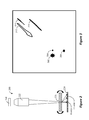
- FIG. 1 is a general schematic depicting major components of a laser-based voltage probe system architecture according to the prior art.
- FIG. 2 is a diagram illustrating the main component of a beam manipulation optics according to an embodiment of the invention.
- FIG. 3 is a schematic illustrating emission obtained from faulty devices using standard optics and with the addition of rotatable grating.
- FIG. 4 is a schematic of elements of an optical path 400 according to another embodiment of the invention.
- FIG. 5 is a schematic of elements of an optical path 500 according to yet another embodiment of the invention.
- FIG. 6 is a schematic of elements of an optical path 600 according to yet another embodiment of the invention.
- FIG. 7 illustrates a plot of arbitrary line scan along an axis of three spectra.
- FIG. 8 illustrates an outline of the emission image (zero order) of a conductive line on the left and an outline of the spectral mapping obtained with the diffraction element on the right.
- FIG. 9 illustrates profile plots along lines perpendicular to the major axis of the spectral mapping shown in FIG. 8 .
- Various embodiments of the present invention provide apparatus and method for non-invasive, non-contact method for probing active transistors within a selected area of the DUT.
- the described methodologies augment the prior art system by enhancing the ability to identify faulty devices or identify working transistors in a wrong state because of surrounding issues like shorts, due to process/design errors, provide improved ability to localize the faulty device even in a highly dense area, and provide method for classifying the fault to assist in failure analysis.
- embodiments of the invention also enable identifying thermal emission. For example, conductor line resistance emission can be identified, i.e., not transistor or device but just resistive metal line emitting heat. The curve or spectral profile in that case is even more exponential than the NMOS in saturation.
- FIG. 2 is a schematic of elements of an optical path 200 according to an embodiment of the invention that may be implemented in any of the prior art optical system for probing DUT 260 .
- Static and dynamic emission proper can especially benefit from this embodiment.
- An objective 222 collect light emitted or reflected from DUT 260 .
- the light may traverse various optical elements that condition the light to be imaged by sensor 224 . These elements are not depicted as they are known in the art and may differ from system to system.
- a rotatable grating 226 is inserted right ahead of the sensor 224 .
- the sensor in this embodiment is an InGaAs camera.
- Other cameras such as e.g., Short Wave Infra Red (SWIR) camera, HgCdTe camera, etc., may be used.
- SWIR Short Wave Infra Red
- HgCdTe camera etc.
- FIG. 3 is a schematic illustrating emission obtained from faulty devices using standard optics with the addition of rotatable grating.
- a transmission grating is used as the diffraction element.
- the transmission grating is adjusted such that both the zero order and first order diffraction are simultaneously visible in the field of view. Consequently, the image of FIG. 3 shows both the emission site (zero order) and the spectra of the emission (first order) sites in the same image. The axis of each spectrum passes through the emission site.
- 302, 304 and 306 are caricatures indicating the image obtained of the emission site of a diode in forward bias, an NMOS in saturation, and an NMOS in tristate, respectively.
- the size of the caricature conforms to the actual round emission image obtained.
- images 312 , 314 and 316 of the spectra of the diode in forward bias, the NMOS in saturation, and the NMOS in tristate, respectively, show clear separation and different character.
- the grating cause the shorter wavelength to be close to the emission site, and longer wavelength further from the emission site.
- the image is projected on a screen monitor, and the shape of the spectra image can be used to identify the type of fault.
- the NMOS in tristate provide a flat spectrum, appearing as an even streak.
- the NMOS in saturation appears like a comet, i.e., tail oriented towards the emission site.
- the “blob” like, or “teardrop” shape head pointing towards the emission site), spectrum of the diode can be easily distinguished from the two NMOS spectra.
- the various faulty devices can be identified, localized and classified using the spectra captured with the rotatable grating.
- the grating was rotated until the best orientation was obtained to enable clear separation of the spectra and then the image captured. In FIG. 3 , rotation to about 45° provided a clear separation of the spectra. Conversely, if the grating was not rotatable, the spectra from the diode and the NMOS in saturation would have overlapped, such that the spectra of these devices would not be separable. Note that the preferred rotational orientation of the grating will depend on the actual orientation of the faulty devices in the field of view. For example, in the case of FIG. 3 , a 90° rotation would have caused the spectra from the two NMOS to overlap.
- the cluster of interest may need to be separated from other clusters or the field of view reduced, which can be achieved using the embodiment illustrated in FIG. 4 .
- FIG. 4 is a schematic of elements of an optical path 400 according to another embodiment of the invention that may be implemented in any of the prior art optical system for probing DUT 460 .
- An objective 422 collects light emitted or reflected from DUT 460 .
- the light may traverse various optical elements that condition the light to be imaged by sensor 424 . These elements are not depicted as they are known in the art and may differ from system to system.
- an adjustable iris 421 is placed in the intermediate image plane defined by the objective 422 .
- the opening size of the iris 421 is controllable and is used to limit the field of view of the optical system 400 .
- the iris 421 can be adjusted both in size and position.
- a rotatable diffraction element 426 is inserted behind the iris 421 .
- the light from the grating 426 passes through a relay lens 423 , which focuses it onto the sensor 424 (final image plane).
- a transmission grating 426 is used as the diffraction element and is positioned so that the zero order and first order are visible in the field of view so that they are both captured by the sensor 424 simultaneously.
- the image of the impinging light would change depending on the rotational orientation of the grating.
- the movable iris 421 assists in separating the light from multiple devices, thereby enabling better localization of the faulty device.
- the iris size is adjusted to let one (or more) emitter light go through and its position is moved in X and Y so that it can be place on that specific emitter, hereby blocking the light of the other emitters in the field of view of the optics.
- SIL solid immersion lens
- the SIL may be used in any of the disclosed embodiments.
- FIG. 5 is a schematic of elements of an optical path 500 according to yet another embodiment of the invention that may be implemented in any of the prior art optical system for probing DUT 560 .
- An objective 522 with SIL 527 collect light emitted or reflected from DUT 560 .
- the light may traverse various optical elements that condition the light to be imaged by sensor 524 . These elements are not depicted as they are known in the art and may differ from system to system.
- a adjustable iris 521 is placed in the image plane defined by the objective 522 .
- the opening size of the iris 521 is controllable and is used to limit the field of view of the optical system 500 .
- a rotatable reflecting grating 526 is inserted behind the iris 521 , in a light path created by the reflecting mirror 528 .
- Mirror 528 may be a collimating mirror.
- the light reflected from the grating 526 passes through a relay lens 523 , which focuses it onto the sensor 524 .
- the image of the impinging light would change depending on the rotational orientation of the reflecting grating 526 .
- references made herein to lens encompass any optical element that acts as a lens, i.e., both transmitting and reflecting elements.
- references made herein to grating encompass any element that diffracts light to its frequency components.
- it encompass, e.g., transmissive grating, reflective grating, prism, tunable filters, e.g., acousto-optical tunable filter, liquid crystal tunable filters, etc.
- the use of transmission grating has been shown to be beneficial in that it is relatively thin, so may be easily inserted in optical path of existing emission systems.
- FIG. 6 is a schematic of elements of an optical path 600 according to yet another embodiment of the invention that may be implemented in any of the prior art optical system for probing DUT 660 .
- An objective 622 collects light emitted or reflected from DUT 660 .
- the light may traverse various optical elements that condition the light to be imaged by sensor 624 . These elements are not depicted as they are known in the art and may differ from system to system.
- the rotatable grating of the prior embodiments is replaced by tunable filter 629 .
- the light from the tunable filter 629 passes onto the sensor 624 .
- the image of the impinging light would change depending on the tuning of the tunable filter 629 .
- the images at different tuning can help classify the fault, but may not be as efficient in localizing the fault as the rotating grating embodiments.
- FIG. 7 illustrates a plot of arbitrary line scan along an axis of three spectra.
- the plot of solid line illustrates a rather monotonous spectrum corresponding to emission such as obtained from, e.g., an NMOS in tristate.
- the plot in dashed-line shows spectrum that is weighted towards the shorter wavelengths. Such spectra is more indicative of the forward biased diode.
- the dotted plot illustrates a spectrum that is more pronounced at the longer wavelength, which would be indicative of an NMOS in saturation.
- embodiments of the invention also enable identifying thermal emission. For example, conductor line resistance emission can be identified, i.e., not transistor or device but just resistive metal line emitting heat.
- a line scan along the axis of each spectra can be used to classify the faults. This can be done by programming computer 170 to perform the line scanning on each obtained spectrum. Therefore, a user may be able to classify the fault by observing the shape of the image of the spectrum and by running a line scan along the axis of the spectrum.
- FIG. 8 illustrates an outline of the emission image (zero order) of a conductive line on the left and an outline of the spectral mapping obtained with the diffraction element on the right.
- the standard emission image appears rather homogeneous, but the spectral image reveals inhomogeneity in the conductive properties of the line. That is, the higher resistance areas appear hotter than the lower resistance areas.
- This can be verified by plotting a spectrum profile along various points on the image, as shown in FIG. 9 , wherein plot 3 appears hotter than plot 1 , thus indicating that there's higher line resistance at the point where plot 3 was taken.
Landscapes
- Physics & Mathematics (AREA)
- Engineering & Computer Science (AREA)
- General Physics & Mathematics (AREA)
- Health & Medical Sciences (AREA)
- Biochemistry (AREA)
- Analytical Chemistry (AREA)
- General Health & Medical Sciences (AREA)
- Chemical & Material Sciences (AREA)
- Immunology (AREA)
- Pathology (AREA)
- Life Sciences & Earth Sciences (AREA)
- Computer Hardware Design (AREA)
- Microelectronics & Electronic Packaging (AREA)
- Computer Vision & Pattern Recognition (AREA)
- Electromagnetism (AREA)
- Toxicology (AREA)
- General Engineering & Computer Science (AREA)
- Tests Of Electronic Circuits (AREA)
- Testing Or Measuring Of Semiconductors Or The Like (AREA)
- Microscoopes, Condenser (AREA)
Priority Applications (2)
| Application Number | Priority Date | Filing Date | Title |
|---|---|---|---|
| US14/657,605 US10041997B2 (en) | 2014-03-13 | 2015-03-13 | System and method for fault isolation by emission spectra analysis |
| US16/027,159 US10620263B2 (en) | 2014-03-13 | 2018-07-03 | System and method for fault isolation by emission spectra analysis |
Applications Claiming Priority (2)
| Application Number | Priority Date | Filing Date | Title |
|---|---|---|---|
| US201461952861P | 2014-03-13 | 2014-03-13 | |
| US14/657,605 US10041997B2 (en) | 2014-03-13 | 2015-03-13 | System and method for fault isolation by emission spectra analysis |
Related Child Applications (1)
| Application Number | Title | Priority Date | Filing Date |
|---|---|---|---|
| US16/027,159 Division US10620263B2 (en) | 2014-03-13 | 2018-07-03 | System and method for fault isolation by emission spectra analysis |
Publications (2)
| Publication Number | Publication Date |
|---|---|
| US20150260789A1 US20150260789A1 (en) | 2015-09-17 |
| US10041997B2 true US10041997B2 (en) | 2018-08-07 |
Family
ID=54068613
Family Applications (2)
| Application Number | Title | Priority Date | Filing Date |
|---|---|---|---|
| US14/657,605 Active 2035-04-18 US10041997B2 (en) | 2014-03-13 | 2015-03-13 | System and method for fault isolation by emission spectra analysis |
| US16/027,159 Active US10620263B2 (en) | 2014-03-13 | 2018-07-03 | System and method for fault isolation by emission spectra analysis |
Family Applications After (1)
| Application Number | Title | Priority Date | Filing Date |
|---|---|---|---|
| US16/027,159 Active US10620263B2 (en) | 2014-03-13 | 2018-07-03 | System and method for fault isolation by emission spectra analysis |
Country Status (3)
| Country | Link |
|---|---|
| US (2) | US10041997B2 (enExample) |
| JP (1) | JP2015175851A (enExample) |
| SG (1) | SG10201501966TA (enExample) |
Families Citing this family (4)
| Publication number | Priority date | Publication date | Assignee | Title |
|---|---|---|---|---|
| SG10201501966TA (en) | 2014-03-13 | 2015-10-29 | Dcg Systems Inc | System and method for fault isolation by emission spectra analysis |
| US9903824B2 (en) | 2014-04-10 | 2018-02-27 | Fei Efa, Inc. | Spectral mapping of photo emission |
| CN106505336B (zh) | 2015-09-07 | 2018-12-14 | 矢崎总业株式会社 | 连接器 |
| WO2024241626A1 (ja) | 2023-05-19 | 2024-11-28 | 浜松ホトニクス株式会社 | 検査装置及び検査方法 |
Citations (25)
| Publication number | Priority date | Publication date | Assignee | Title |
|---|---|---|---|---|
| US3601492A (en) * | 1967-11-20 | 1971-08-24 | Monsanto Co | Apparatus for measuring film thickness |
| US5208648A (en) | 1991-03-11 | 1993-05-04 | International Business Machines Corporation | Apparatus and a method for high numerical aperture microscopic examination of materials |
| US5220403A (en) | 1991-03-11 | 1993-06-15 | International Business Machines Corporation | Apparatus and a method for high numerical aperture microscopic examination of materials |
| US5289260A (en) * | 1990-11-09 | 1994-02-22 | Mitsubishi Denki Kabushiki Kaisha | Pattern defect detection device and a spatial frequency filter used therein |
| US5940545A (en) | 1996-07-18 | 1999-08-17 | International Business Machines Corporation | Noninvasive optical method for measuring internal switching and other dynamic parameters of CMOS circuits |
| US6064477A (en) * | 1993-02-26 | 2000-05-16 | Hitachi, Ltd. | Method of and apparatus for inspecting reticle for defects |
| US6081325A (en) * | 1996-06-04 | 2000-06-27 | Kla-Tencor Corporation | Optical scanning system for surface inspection |
| US6263099B1 (en) * | 1994-10-07 | 2001-07-17 | Hitachi, Ltd. | Manufacturing method of semiconductor substrate and method and apparatus for inspecting defects of patterns of an object to be inspected |
| US20040146295A1 (en) * | 2003-01-15 | 2004-07-29 | Negevtech Ltd. | System for detection of wafer defects |
| US20050168730A1 (en) * | 2001-04-03 | 2005-08-04 | Hitachi, Ltd. | Method and apparatus for inspecting defects |
| US6943572B2 (en) | 2002-09-03 | 2005-09-13 | Credence Systems Corporation | Apparatus and method for detecting photon emissions from transistors |
| US7012537B2 (en) | 2004-02-10 | 2006-03-14 | Credence Systems Corporation | Apparatus and method for determining voltage using optical observation |
| US7038442B2 (en) | 2002-09-03 | 2006-05-02 | Credence Systems Corporation | Apparatus and method for detecting photon emissions from transistors |
| US7224828B2 (en) | 2001-11-28 | 2007-05-29 | Credence Systems Corporation | Time resolved non-invasive diagnostics system |
| US7295301B2 (en) * | 2002-07-09 | 2007-11-13 | Kla-Tencor Technologies Corporation | Dual stage defect region identification and defect detection method and apparatus |
| US20090002717A1 (en) * | 1999-07-26 | 2009-01-01 | Attofemto, Inc. | Condition assessment system for a structure including a semiconductor material |
| US20090046288A1 (en) * | 2007-08-13 | 2009-02-19 | Jds Uniphase Corporation | Scanning Spectrometer With Multiple Photodetectors |
| TW200944821A (en) | 2007-12-07 | 2009-11-01 | Freescale Semiconductor Inc | Method for testing a semiconductor device and a semiconductor device testing system |
| CN101344731B (zh) | 2007-06-29 | 2011-01-12 | Asml荷兰有限公司 | 用于透射图像感应的装置和方法 |
| US20110043775A1 (en) | 2009-08-20 | 2011-02-24 | Asml Netherlands B.V. | Lithographic apparatus, distortion determining method, and patterning device |
| US20110242312A1 (en) * | 2010-03-30 | 2011-10-06 | Lasertec Corporation | Inspection system and inspection method |
| US8416402B2 (en) * | 2008-04-16 | 2013-04-09 | Hitachi High-Technologies Corporation | Method and apparatus for inspecting defects |
| US20130314710A1 (en) * | 2000-09-20 | 2013-11-28 | Kla-Tencor Technologies Corporation | Methods and Systems for Determining a Critical Dimension and Overlay of a Specimen |
| JP2015175851A (ja) | 2014-03-13 | 2015-10-05 | ディーシージー システムズ、 インコーポライテッドDcg Systems Inc. | 発光スペクトル分析による欠陥の分離のためのシステムと方法 |
| US20150293037A1 (en) | 2014-04-10 | 2015-10-15 | Dcg Systems, Inc. | Spectral mapping of photo emission |
Family Cites Families (11)
| Publication number | Priority date | Publication date | Assignee | Title |
|---|---|---|---|---|
| DE19701703A1 (de) * | 1997-01-21 | 1998-07-23 | Zeiss Carl Jena Gmbh | Mikroskopisches System zur Erfassung der Emissionsverteilung und Verfahren zu dessen Betrieb |
| US6051828A (en) * | 1997-07-02 | 2000-04-18 | Texas Instruments Incorporated | Light emission noise detection and characterization |
| JP3950608B2 (ja) * | 2000-01-18 | 2007-08-01 | 株式会社ルネサステクノロジ | エミッション顕微鏡を用いた不良解析方法およびそのシステム並びに半導体装置の製造方法 |
| JP2001319955A (ja) * | 2000-05-10 | 2001-11-16 | Hitachi Ltd | 発光解析方法およびその装置 |
| JP2002014145A (ja) * | 2000-06-29 | 2002-01-18 | Hamamatsu Photonics Kk | 半導体デバイス検査装置及び半導体デバイス検査方法 |
| JP4485904B2 (ja) * | 2004-10-18 | 2010-06-23 | 株式会社日立ハイテクノロジーズ | 検査装置及び検査方法 |
| US7733100B2 (en) * | 2005-08-26 | 2010-06-08 | Dcg Systems, Inc. | System and method for modulation mapping |
| JP4928862B2 (ja) * | 2006-08-04 | 2012-05-09 | 株式会社日立ハイテクノロジーズ | 欠陥検査方法及びその装置 |
| JP5007979B2 (ja) * | 2008-05-22 | 2012-08-22 | 独立行政法人産業技術総合研究所 | 欠陥を検査する方法及び欠陥検査装置 |
| US20120326060A1 (en) * | 2011-06-22 | 2012-12-27 | Boaz Kenane | Testing method for led wafer |
| US8867580B2 (en) * | 2012-05-15 | 2014-10-21 | Finisar Corporation | Wavelength tunable laser |
-
2015
- 2015-03-13 SG SG10201501966TA patent/SG10201501966TA/en unknown
- 2015-03-13 US US14/657,605 patent/US10041997B2/en active Active
- 2015-03-13 JP JP2015051375A patent/JP2015175851A/ja active Pending
-
2018
- 2018-07-03 US US16/027,159 patent/US10620263B2/en active Active
Patent Citations (29)
| Publication number | Priority date | Publication date | Assignee | Title |
|---|---|---|---|---|
| US3601492A (en) * | 1967-11-20 | 1971-08-24 | Monsanto Co | Apparatus for measuring film thickness |
| US5289260A (en) * | 1990-11-09 | 1994-02-22 | Mitsubishi Denki Kabushiki Kaisha | Pattern defect detection device and a spatial frequency filter used therein |
| US5208648A (en) | 1991-03-11 | 1993-05-04 | International Business Machines Corporation | Apparatus and a method for high numerical aperture microscopic examination of materials |
| US5220403A (en) | 1991-03-11 | 1993-06-15 | International Business Machines Corporation | Apparatus and a method for high numerical aperture microscopic examination of materials |
| US6064477A (en) * | 1993-02-26 | 2000-05-16 | Hitachi, Ltd. | Method of and apparatus for inspecting reticle for defects |
| US6263099B1 (en) * | 1994-10-07 | 2001-07-17 | Hitachi, Ltd. | Manufacturing method of semiconductor substrate and method and apparatus for inspecting defects of patterns of an object to be inspected |
| US20020154303A1 (en) * | 1994-10-07 | 2002-10-24 | Shunji Maeda | Manufacturing method of semiconductor substrate and method and apparatus for inspecting defects of patterns on an object to be inspected |
| US6081325A (en) * | 1996-06-04 | 2000-06-27 | Kla-Tencor Corporation | Optical scanning system for surface inspection |
| US5940545A (en) | 1996-07-18 | 1999-08-17 | International Business Machines Corporation | Noninvasive optical method for measuring internal switching and other dynamic parameters of CMOS circuits |
| US20090002717A1 (en) * | 1999-07-26 | 2009-01-01 | Attofemto, Inc. | Condition assessment system for a structure including a semiconductor material |
| US20130314710A1 (en) * | 2000-09-20 | 2013-11-28 | Kla-Tencor Technologies Corporation | Methods and Systems for Determining a Critical Dimension and Overlay of a Specimen |
| US20050168730A1 (en) * | 2001-04-03 | 2005-08-04 | Hitachi, Ltd. | Method and apparatus for inspecting defects |
| US7224828B2 (en) | 2001-11-28 | 2007-05-29 | Credence Systems Corporation | Time resolved non-invasive diagnostics system |
| US7295301B2 (en) * | 2002-07-09 | 2007-11-13 | Kla-Tencor Technologies Corporation | Dual stage defect region identification and defect detection method and apparatus |
| US7323862B2 (en) | 2002-09-03 | 2008-01-29 | Credence Systems Corporation | Apparatus and method for detecting photon emissions from transistors |
| US6943572B2 (en) | 2002-09-03 | 2005-09-13 | Credence Systems Corporation | Apparatus and method for detecting photon emissions from transistors |
| US7038442B2 (en) | 2002-09-03 | 2006-05-02 | Credence Systems Corporation | Apparatus and method for detecting photon emissions from transistors |
| US20040146295A1 (en) * | 2003-01-15 | 2004-07-29 | Negevtech Ltd. | System for detection of wafer defects |
| US7012537B2 (en) | 2004-02-10 | 2006-03-14 | Credence Systems Corporation | Apparatus and method for determining voltage using optical observation |
| CN101344731B (zh) | 2007-06-29 | 2011-01-12 | Asml荷兰有限公司 | 用于透射图像感应的装置和方法 |
| US20090046288A1 (en) * | 2007-08-13 | 2009-02-19 | Jds Uniphase Corporation | Scanning Spectrometer With Multiple Photodetectors |
| TW200944821A (en) | 2007-12-07 | 2009-11-01 | Freescale Semiconductor Inc | Method for testing a semiconductor device and a semiconductor device testing system |
| US8416402B2 (en) * | 2008-04-16 | 2013-04-09 | Hitachi High-Technologies Corporation | Method and apparatus for inspecting defects |
| US20110043775A1 (en) | 2009-08-20 | 2011-02-24 | Asml Netherlands B.V. | Lithographic apparatus, distortion determining method, and patterning device |
| US20110242312A1 (en) * | 2010-03-30 | 2011-10-06 | Lasertec Corporation | Inspection system and inspection method |
| JP2015175851A (ja) | 2014-03-13 | 2015-10-05 | ディーシージー システムズ、 インコーポライテッドDcg Systems Inc. | 発光スペクトル分析による欠陥の分離のためのシステムと方法 |
| US20150293037A1 (en) | 2014-04-10 | 2015-10-15 | Dcg Systems, Inc. | Spectral mapping of photo emission |
| TW201538965A (zh) | 2014-04-10 | 2015-10-16 | Dcg系統公司 | 光子發射的光譜套圖 |
| JP2015203700A (ja) | 2014-04-10 | 2015-11-16 | ディーシージー システムズ、 インコーポライテッドDcg Systems Inc. | 光子放出のスペクトルマッピング |
Non-Patent Citations (16)
| Title |
|---|
| Black, A., et al. "Optical Sampling of GHz Charge Density Modulation in Silicon Bipolar Junction Transistors," Electronics Letters, vol. 23, No. 15, 1987, p. 783-784. |
| Bruce, M., et al. "Waveform Acquisition from the Backside of Silicon Using Electro-Optic Probing," Proceedings from the 25th International Symposium for Testing and Failure Analysis, Nov. 1999, pp. 19-25. |
| Heinrich, H.K., "Picosecond Noninvasive Optical Detection of Internal Electrical Signals in Flip-Chip-Mounted Silicon Integrated Circuits," IBM Journal of Research and Development, vol. 34, Issue 2/3, 1990, p. 162-172. |
| Heinrich, H.K., et al. "Erratum: Noninvasive Sheet Charge Density Probe for Integrated Silicon Devices," Applied Physics Letters, vol. 48, Issue 26, Jun. 1986, p. 1811. |
| Heinrich, H.K., et al. "Measurement of Real-Time Digital Signals in a Silicon Bipolar Junction Transistor Using a Noninvasive Optical Probe," IEEE Electronics Letters, vol. 22, No. 12, Jun. 1986, pp. 650-652. |
| Heinrich, H.K., et al. "Noninvasive Sheet Charge Density Probe for Integrated Silicon Devices," Applied Physics Letters, vol. 48, Issue 16, Apr. 1986, p. 1066-1068. |
| Hemenway, B.R., et al. "Optical Detection of Charge Modulation in Silicon Integrated Circuits Using a Multimode Laser-Diode Probe," IEEE Electron Device Letters, vol. 8, No. 8, Aug. 1987, pp. 344-346. |
| Kasapi, S., et al. "Laser Beam Backside Probing of CMOS Integrated Circuits," Microelectronics Reliability, vol. 39, 1999, pp. 957-961. |
| Kindereit, U., et al. "Comparison of Laser Voltage Probing and Mapping Results in Oversized and Minimum Size Devices of 120nm and 65nm Technology," Microelectronics Reliability, vol. 48, Issues 8/9, Sep. 2008, pp. 1322-1326, 19th European Symposium on Reliability of Electron Devices, Failure Physics and Analysis (ESREF 2008). |
| Kolachina, S., et al. "Optical Waveform Probing-Strategies for Non-Flipchip Devices and Other Applications," Conference Proceedings from the 27th International Symposium for Testing and Failure Analysis (ISFTA), Nov. 2001, pp. 51-57. |
| Notice of Allowance for Taiwanese Patent Application No. 104111375 dated Jun. 13, 2016. |
| Rusu, S., et al. "Backside Infrared Probing for Static Voltage Drop and Dynamic Timing Measurements," 2001 IEEE International Solid-State Circuits Conference (ISSCC), Feb. 2001, Digest of Technical Papers, pp. 276-277. |
| Scholz, P., et al. "Single image spectral electroluminescence (photon emission) of GaN HEMTs," 2013 IEEE International Reliability Physics Symposium (IRPS), Apr. 2013, pp. CD.3.1-CD.3.7. |
| Soref, R.A., et al. "Electrooptical Effects in Silicon," IEEE Journal of Quantum Electronics, vol. QE-23, Issue 1, Jan. 1987, pp. 123-129. |
| Wilsher, K., et al. "Integrated Circuit Waveform Probing Using Optical Phase Shift Detection," Proceedings from the 26th International Symposium for Testing and Failure Analysis, Nov. 2000, pp. 479-485. |
| Yee, W. M., et al. "Laser Voltage Probe (LVP): A Novel Optical Probing Technology for Flip-Chip Packaged Microprocessors," Conference Proceedings from the 26th International Symposium for Testing and Failure Analysis (ISFTA), Nov. 2000, pp. 3-8. |
Also Published As
| Publication number | Publication date |
|---|---|
| US20150260789A1 (en) | 2015-09-17 |
| US20180328985A1 (en) | 2018-11-15 |
| US10620263B2 (en) | 2020-04-14 |
| SG10201501966TA (en) | 2015-10-29 |
| JP2015175851A (ja) | 2015-10-05 |
Similar Documents
| Publication | Publication Date | Title |
|---|---|---|
| US9903824B2 (en) | Spectral mapping of photo emission | |
| US6967491B2 (en) | Spatial and temporal selective laser assisted fault localization | |
| US9915700B2 (en) | System and method for modulation mapping | |
| US10620263B2 (en) | System and method for fault isolation by emission spectra analysis | |
| JP5993909B2 (ja) | レーザ電圧画像化状態マッピングのためのシステム | |
| US20050002028A1 (en) | Time resolved emission spectral analysis system | |
| KR20050002819A (ko) | 집적 회로의 동적 진단 테스트를 위한 장치 및 방법 | |
| US9739831B2 (en) | Defect isolation methods and systems | |
| Niu et al. | Laser logic state imaging (llsi) | |
| US20050036151A1 (en) | Method and device for opically testing semiconductor elements | |
| TWI769229B (zh) | 半導體檢查裝置 | |
| US7616312B2 (en) | Apparatus and method for probing integrated circuits using laser illumination | |
| US11967061B2 (en) | Semiconductor apparatus examination method and semiconductor apparatus examination apparatus | |
| JP2016109673A (ja) | レーザボルテージイメージングのシステム及び方法 | |
| US20170176520A1 (en) | Tunable wavelength electro-optical analyzer | |
| Kasapi et al. | Comparison of applications of laser probing, laser-induced circuit perturbation and photon emission for failure analysis and yield enhancement | |
| US9417281B1 (en) | Adjustable split-beam optical probing (ASOP) | |
| Miller et al. | At-Speed Defect Localization by Combining Laser Scanning Microscopy and Power Spectrum Analysis | |
| Ferrigno et al. | Identification of Process/Design Issues during 0.18 μm Technology Qualification for Space Application | |
| Stoker et al. | Pump-Probe Imaging of Integrated Circuits |
Legal Events
| Date | Code | Title | Description |
|---|---|---|---|
| AS | Assignment |
Owner name: DCG SYSTEMS, INC., CALIFORNIA Free format text: ASSIGNMENT OF ASSIGNORS INTEREST;ASSIGNORS:DESLANDES, HERVE;SABBINENI, PRASAD;FREED, REGINA;SIGNING DATES FROM 20150317 TO 20150319;REEL/FRAME:035831/0432 |
|
| AS | Assignment |
Owner name: FEI EFA, INC., CALIFORNIA Free format text: CHANGE OF NAME;ASSIGNOR:DCG SYSTEMS, INC.;REEL/FRAME:042642/0402 Effective date: 20160523 |
|
| FEPP | Fee payment procedure |
Free format text: ENTITY STATUS SET TO UNDISCOUNTED (ORIGINAL EVENT CODE: BIG.); ENTITY STATUS OF PATENT OWNER: LARGE ENTITY |
|
| STCF | Information on status: patent grant |
Free format text: PATENTED CASE |
|
| MAFP | Maintenance fee payment |
Free format text: PAYMENT OF MAINTENANCE FEE, 4TH YEAR, LARGE ENTITY (ORIGINAL EVENT CODE: M1551); ENTITY STATUS OF PATENT OWNER: LARGE ENTITY Year of fee payment: 4 |