US10031294B2 - Optical switch and wavelength division multiplexing optical system - Google Patents
Optical switch and wavelength division multiplexing optical system Download PDFInfo
- Publication number
- US10031294B2 US10031294B2 US15/360,642 US201615360642A US10031294B2 US 10031294 B2 US10031294 B2 US 10031294B2 US 201615360642 A US201615360642 A US 201615360642A US 10031294 B2 US10031294 B2 US 10031294B2
- Authority
- US
- United States
- Prior art keywords
- micromirror
- output
- input
- subarray
- array
- Prior art date
- Legal status (The legal status is an assumption and is not a legal conclusion. Google has not performed a legal analysis and makes no representation as to the accuracy of the status listed.)
- Expired - Fee Related, expires
Links
Images


Classifications
-
- G—PHYSICS
- G02—OPTICS
- G02B—OPTICAL ELEMENTS, SYSTEMS OR APPARATUS
- G02B6/00—Light guides; Structural details of arrangements comprising light guides and other optical elements, e.g. couplings
- G02B6/24—Coupling light guides
- G02B6/26—Optical coupling means
- G02B6/35—Optical coupling means having switching means
- G02B6/351—Optical coupling means having switching means involving stationary waveguides with moving interposed optical elements
- G02B6/3512—Optical coupling means having switching means involving stationary waveguides with moving interposed optical elements the optical element being reflective, e.g. mirror
- G02B6/3518—Optical coupling means having switching means involving stationary waveguides with moving interposed optical elements the optical element being reflective, e.g. mirror the reflective optical element being an intrinsic part of a MEMS device, i.e. fabricated together with the MEMS device
-
- G—PHYSICS
- G02—OPTICS
- G02B—OPTICAL ELEMENTS, SYSTEMS OR APPARATUS
- G02B26/00—Optical devices or arrangements for the control of light using movable or deformable optical elements
- G02B26/08—Optical devices or arrangements for the control of light using movable or deformable optical elements for controlling the direction of light
- G02B26/0816—Optical devices or arrangements for the control of light using movable or deformable optical elements for controlling the direction of light by means of one or more reflecting elements
- G02B26/0833—Optical devices or arrangements for the control of light using movable or deformable optical elements for controlling the direction of light by means of one or more reflecting elements the reflecting element being a micromechanical device, e.g. a MEMS mirror, DMD
-
- G—PHYSICS
- G02—OPTICS
- G02B—OPTICAL ELEMENTS, SYSTEMS OR APPARATUS
- G02B6/00—Light guides; Structural details of arrangements comprising light guides and other optical elements, e.g. couplings
- G02B6/24—Coupling light guides
- G02B6/26—Optical coupling means
- G02B6/35—Optical coupling means having switching means
- G02B6/351—Optical coupling means having switching means involving stationary waveguides with moving interposed optical elements
- G02B6/3512—Optical coupling means having switching means involving stationary waveguides with moving interposed optical elements the optical element being reflective, e.g. mirror
- G02B6/352—Optical coupling means having switching means involving stationary waveguides with moving interposed optical elements the optical element being reflective, e.g. mirror the reflective optical element having a shaped reflective surface, e.g. a reflective element comprising several reflective surfaces or facets that function together
-
- G—PHYSICS
- G02—OPTICS
- G02B—OPTICAL ELEMENTS, SYSTEMS OR APPARATUS
- G02B6/00—Light guides; Structural details of arrangements comprising light guides and other optical elements, e.g. couplings
- G02B6/24—Coupling light guides
- G02B6/26—Optical coupling means
- G02B6/35—Optical coupling means having switching means
- G02B6/354—Switching arrangements, i.e. number of input/output ports and interconnection types
- G02B6/3542—Non-blocking switch, e.g. with multiple potential paths between multiple inputs and outputs, the establishment of one switching path not preventing the establishment of further switching paths
-
- H—ELECTRICITY
- H04—ELECTRIC COMMUNICATION TECHNIQUE
- H04J—MULTIPLEX COMMUNICATION
- H04J14/00—Optical multiplex systems
- H04J14/02—Wavelength-division multiplex systems
-
- G—PHYSICS
- G02—OPTICS
- G02B—OPTICAL ELEMENTS, SYSTEMS OR APPARATUS
- G02B6/00—Light guides; Structural details of arrangements comprising light guides and other optical elements, e.g. couplings
- G02B6/24—Coupling light guides
- G02B6/26—Optical coupling means
- G02B6/35—Optical coupling means having switching means
- G02B6/351—Optical coupling means having switching means involving stationary waveguides with moving interposed optical elements
- G02B6/3512—Optical coupling means having switching means involving stationary waveguides with moving interposed optical elements the optical element being reflective, e.g. mirror
-
- G—PHYSICS
- G02—OPTICS
- G02B—OPTICAL ELEMENTS, SYSTEMS OR APPARATUS
- G02B6/00—Light guides; Structural details of arrangements comprising light guides and other optical elements, e.g. couplings
- G02B6/24—Coupling light guides
- G02B6/26—Optical coupling means
- G02B6/35—Optical coupling means having switching means
- G02B6/354—Switching arrangements, i.e. number of input/output ports and interconnection types
- G02B6/3554—3D constellations, i.e. with switching elements and switched beams located in a volume
- G02B6/3556—NxM switch, i.e. regular arrays of switches elements of matrix type constellation
-
- H—ELECTRICITY
- H04—ELECTRIC COMMUNICATION TECHNIQUE
- H04Q—SELECTING
- H04Q11/00—Selecting arrangements for multiplex systems
- H04Q11/0001—Selecting arrangements for multiplex systems using optical switching
- H04Q11/0005—Switch and router aspects
- H04Q2011/0007—Construction
Definitions
- the present invention relates to the field of optical communications, and in particular, to an optical switch and a wavelength division multiplexing optical system in the communications field.
- An all-optical communications network is a high-speed broadband communications network that is based on a dense wavelength division multiplexing (DWDM) technology.
- the all-optical communications network uses the DWDM technology on a backbone for capacity expansion, is implemented on a switching node by using an optical add-drop multiplexer (OADM) and an optical cross-connector (OXC), and implements fiber to the home (FTTH) by using a fiber-to-the-x technology.
- the OXC and the OADM are core components of the all-optical communications network, and developing the optical cross-connector (OXC) and the optical add-drop multiplexer (OADM) becomes a very urgent task for constructing a large-capacity communications backbone network.
- Cores of the OXC and the OADM are optical switches and optical switch arrays.
- a switching node of a metropolitan area network and a backbone network in a wavelength division multiplexing (WDM) optical network has an increasingly high requirement for a throughput capacity, and an OXC device and an OADM device of the switching node also have increasingly large scale, technologically, an optical switch is required to have larger scale and higher integration.
- a current optical switch cannot meet a requirement of the switching node of the metropolitan area network and the backbone network for a throughput capacity.
- embodiments of the present invention provide an optical switch and a wavelength division multiplexing optical system, which can meet a requirement of a switching node for a throughput capacity.
- an optical switch includes: an input port array, an input collimator array connected to the input port array, an input micromirror array, an output micromirror array, an output collimator array, and an output port array connected to the output collimator array, where
- the input collimator array is configured to perform collimation and beam expansion on an optical signal input through the input port array, and make the optical signal, on which collimation and beam expansion have been performed, be incident on the input micromirror array;
- the input micromirror array is configured to reflect the optical signal, output by the input collimator array, onto the output micromirror array;
- the output micromirror array is configured to reflect the optical signal, reflected by the input micromirror array, onto the output collimator array;
- the output collimator array is configured to couple the optical signal, reflected by the output micromirror array, to the output port array;
- all input micromirrors included in the input micromirror array can be deflected in two mutually perpendicular directions, and maximum movable ranges of reflected light that is output after all the input micromirrors reflect incident light with a same incident angle have no common intersection on a plane on which the output micromirror array is located; or
- maximum movable ranges of reflected light that is output after all the input micromirrors reflect incident light with a same incident angle have a common intersection on a plane on which the output micromirror array is located, and an area of the common intersection is less than an area of a reflection region of the output micromirror array.
- the input micromirror array includes N input micromirror subarrays
- the output micromirror array includes N output micromirror subarrays
- the j th input micromirror subarray of the input micromirror array includes an input adjacent region, and an input micromirror in the input adjacent region can reflect the optical signal onto an output micromirror in the k th output micromirror subarray, where the k th output micromirror subarray is adjacent to the j th output micromirror subarray, j and k are natural numbers, and j and k are less than or equal to N.
- a first input port included in the input port array is connected, by using a fiber, to a first output port included in the output port array, so that the optical signal input through a second input port included in the input port array can be output through any second output port included in the output port array.
- N is 6; the i th input micromirror subarray I i includes two input micromirror regions I i,1 and I i,2 ; the i th output micromirror subarray O i includes two output micromirror regions O i,1 and O i,2 ; each input micromirror in the input micromirror region I 1,2 can reflect the optical signal onto each output micromirror in the output micromirror region O 2,1 ; each input micromirror in I 2,1 adjacent to the input micromirror region I 1,2 can reflect the optical signal onto each output micromirror in O 1,2 adjacent to the output micromirror region O 2,1 ; each input micromirror in the input micromirror region I 3,2 can reflect the optical signal onto each output micromirror in the output micromirror region O 4,1 ; each input micromirror in I 4,1 adjacent to the input micromirmir
- the input micromirror regions I i,1 and separately include L/2 input micromirrors
- the output micromirror regions O i,1 and O i,2 separately include L/2 output micromirrors, where L is an even number.
- each input micromirror subarray includes M input micromirrors
- each output micromirror subarray includes M output micromirrors, where M is a natural number.
- the i th input micromirror subarray including M input micromirrors and the i th output micromirror subarray including M output micromirrors form the i th micromirror subarray pair
- each first micromirror subarray pair corresponds to S input ports in the input port array and 2S ⁇ 1 output ports in the output port array
- each second micromirror subarray pair corresponds to R input ports in the input port array and R output ports in the output port array
- each third micromirror subarray pair corresponds to 2S ⁇ 1 input ports in the input port array and S output ports in the output port array
- the y th output port O 1 x,y corresponding to the x th first micromirror subarray pair and the x th input port I 2 y,x corresponding to the y th second micromirror subarray pair are connected by using a fiber
- the input micromirror included in the input micromirror array and the output micromirror included in the output micromirror array are micro-electro-mechanical system MEMS micromirrors.
- a wavelength division multiplexing optical system includes an optical switch according to an embodiment of the present invention, m1 demultiplexers DEMUXes, and m2 multiplexers MUXes, where
- the optical switch includes: an input port array, an input collimator array connected to the input port array, an input micromirror array, an output micromirror array, an output collimator array, and an output port array connected to the output collimator array;
- the input collimator array is configured to perform collimation and beam expansion on an optical signal input through the input port array, and make the optical signal, on which collimation and beam expansion have been performed, be incident on the input micromirror array;
- the input micromirror array is configured to reflect the optical signal, output by the input collimator array, onto the output micromirror array;
- the output micromirror array is configured to reflect the optical signal, reflected by the input micromirror array, onto the output collimator array;
- the output collimator array is configured to couple the optical signal, reflected by the output micromirror array, to the output port array;
- all input micromirrors included in the input micromirror array can be deflected in two mutually perpendicular directions, and maximum movable ranges of reflected light that is output after all the input micromirrors reflect incident light with a same incident angle have no common intersection on a plane on which the output micromirror array is located; or
- maximum movable ranges of reflected light that is output after all the input micromirrors reflect incident light with a same incident angle have a common intersection on a plane on which the output micromirror array is located, and an area of the common intersection is less than an area of a reflection region of the output micromirror array;
- the input micromirror array includes N input micromirror subarrays
- the output micromirror array includes N output micromirror subarrays
- the input micromirror included in the input micromirror array and the output micromirror included in the output micromirror array are micro-electro-mechanical system MEMS micromirrors;
- the input port array includes N input port subarrays
- the input collimator array includes N input collimator subarrays
- the output port array includes N output port subarrays
- the output collimator array includes N output collimator subarrays, where each input port subarray corresponds to one input collimator subarray and one input micromirror subarray, and each output port subarray corresponds to one output collimator subarray and one output micromirror subarray;
- each input port subarray includes M1 input ports
- each output port subarray includes M2 output ports
- the l1 th input port in the i th input port subarray is connected to a port that is of the l1 th demultiplexer DEMUX of a wavelength division multiplexing WDM system and through which the i th wavelength-combined optical signal is output
- the l2 th output port in the i th output port subarray is connected to a port that is of the l2 th multiplexer MUX of the WDM system and through which the i th wavelength-combined optical signal is input
- M1, M2, l1, and l2 are natural numbers
- the wavelength-combined optical signal includes at least two wavelengths.
- an optical switch includes: an input port array, an input collimator array connected to the input port array, an input micromirror array, an output micromirror array, an output collimator array, and an output port array connected to the output collimator array, where
- the input collimator array is configured to perform collimation and beam expansion on an optical signal input through the input port array, and make the optical signal, on which collimation and beam expansion have been performed, be incident on the input micromirror array;
- the input micromirror array is configured to reflect the optical signal, output by the input collimator array, onto the output micromirror array;
- the output micromirror array is configured to reflect the optical signal, reflected by the input micromirror array, onto the output collimator array;
- the output collimator array is configured to couple the optical signal, reflected by the output micromirror array, to the output port array;
- the input micromirror array includes at least a first input micromirror subarray and a second input micromirror subarray
- the output micromirror array includes at least a third output micromirror subarray and a fourth output micromirror subarray
- incident light can be incident within a reflection region of the third output micromirror subarray after being reflected by the first input micromirror subarray, and the incident light cannot be incident within a reflection region of the fourth output micromirror subarray after being reflected by the first input micromirror subarray
- incident light can be incident within the reflection region of the fourth output micromirror subarray after being reflected by the second input micromirror subarray.
- the input micromirror array includes N input micromirror subarrays
- the output micromirror array includes N output micromirror subarrays
- the output micromirror array further includes a fifth output micromirror subarray, and the incident light can also be incident within a reflection region of the fifth output micromirror subarray after being reflected by the first input micromirror subarray, where the third output micromirror subarray and the fifth output micromirror subarray are adjacent micromirror arrays.
- a first input port included in the input port array is connected, by using a fiber, to a first output port included in the output port array, so that the optical signal input through a second input port included in the input port array can be output through any second output port included in the output port array.
- the input micromirror array includes N input micromirror subarrays, and the i th input micromirror subarray of the N input micromirror subarrays includes two input micromirror subregions I i,1 and I i,2 ;
- the output micromirror array includes N output micromirror subarrays, and the i th output micromirror subarray of the N output micromirror subarrays includes two output micromirror subregions O i,1 and O i,2 ; each input micromirror in the input micromirror subregion I 1,2 can reflect the optical signal onto each output micromirror in the output micromirror subregion O 2,1 ; each input micromirror in I 2,1 adjacent to the input micromirror subregion I 1,2 can reflect the optical signal onto each output micromirror in O 1,2 adjacent to the output micromirror subregion O
- the input micromirror subregions I i,1 and I i,2 separately include L/2 input micromirrors
- the output micromirror subregions O i,1 and O i,2 separately include L/2 output micromirrors, where L is an even number.
- each input micromirror subarray includes M input micromirrors
- each output micromirror subarray includes M output micromirrors, where M is a natural number.
- the i th input micromirror subarray including M input micromirrors and the i th output micromirror subarray including M output micromirrors form the i th micromirror subarray pair
- each first micromirror subarray pair corresponds to S input ports in the input port array and 2S ⁇ 1 output ports in the output port array
- each second micromirror subarray pair corresponds to R input ports in the input port array and R output ports in the output port array
- each third micromirror subarray pair corresponds to 2S ⁇ 1 input ports in the input port array and S output ports in the output port array
- the y th output port O 1 x,y corresponding to the x th first micromirror subarray pair and the x th input port I 2 y,x corresponding to the y th second micromirror subarray pair are connected by using a fiber
- the input micromirror included in the input micromirror array and the output micromirror included in the output micromirror array are micro-electro-mechanical system MEMS micromirrors.
- a wavelength division multiplexing optical system includes an optical switch according to an embodiment of the present invention, m1 demultiplexers DEMUXes, and m2 multiplexers MUXes, where
- the input port array includes N input port subarrays
- the input collimator array includes N input collimator subarrays
- the output port array includes N output port subarrays
- the output collimator array includes N output collimator subarrays, where each input port subarray corresponds to one input collimator subarray and one input micromirror subarray, and each output port subarray corresponds to one output collimator subarray and one output micromirror subarray;
- each input port subarray includes M1 input ports
- each output port subarray includes M2 output ports
- the l1 th input port in the i th input port subarray is connected to a port that is of the l2 th demultiplexer DEMUX of a wavelength division multiplexing WDM system and through which the i th wavelength-combined optical signal is output
- the l2 th output port in the i th output port subarray is connected to a port that is of the l2 th multiplexer MUX of the WDM system and through which the i th wavelength-combined optical signal is input
- the optical switch includes: an input port array, an input collimator array connected to the input port array, an input micromirror array, an output micromirror array, an output collimator array, and an output port array connected to the output collimator array;
- the input collimator array is configured to perform collimation and beam expansion on an optical signal input through the input port array, and make the optical signal, on which collimation and beam expansion have been performed, be incident on the input micromirror array;
- the input micromirror array is configured to reflect the optical signal, output by the input collimator array, onto the output micromirror array;
- the output micromirror array is configured to reflect the optical signal, reflected by the input micromirror array, onto the output collimator array;
- the output collimator array is configured to couple the optical signal, reflected by the output micromirror array, to the output port array;
- the input micromirror array includes at least a first input micromirror subarray and a second input micromirror subarray
- the output micromirror array includes at least a third output micromirror subarray and a fourth output micromirror subarray
- incident light can be incident within a reflection region of the third output micromirror subarray after being reflected by the first input micromirror subarray, and the incident light cannot be incident within a reflection region of the fourth output micromirror subarray after being reflected by the first input micromirror subarray
- incident light can be incident within the reflection region of the fourth output micromirror subarray after being reflected by the second input micromirror subarray
- the input micromirror array includes N input micromirror subarrays
- the output micromirror array includes N output micromirror subarrays
- the input micromirror included in the input micromirror array and the output micromirror included in the output micromirror array are micro-electro-mechanical system MEMS micromirrors.
- the wavelength-combined optical signal includes at least two wavelengths.
- the optical switch and the wavelength division multiplexing optical system are designed as that maximum movable ranges of reflected light that is output after all input micromirrors reflect incident light with a same incident angle have no common intersection on a plane on which an output micromirror array is located; or maximum movable ranges of reflected light that is output after all input micromirrors reflect incident light with a same incident angle have a common intersection on a plane on which an output micromirror array is located, and an area of the common intersection is less than an area of a reflection region of the output micromirror array, which can implement a large-scale array, and therefore can meet a requirement of a switching node for a throughput capacity.
- FIG. 1 is a schematic block diagram of an optical switch according to an embodiment of the present invention
- FIG. 2 is a schematic block diagram of an input micromirror according to an embodiment of the present invention.
- FIG. 3 is a schematic block diagram of an input micromirror array and an output micromirror array according to an embodiment of the present invention
- FIG. 4 is another schematic block diagram of an optical switch according to an embodiment of the present invention.
- FIG. 5 is still another schematic block diagram of an optical switch according to an embodiment of the present invention.
- FIG. 6 is a schematic block diagram of an optical switch according to another embodiment of the present invention.
- FIG. 7 is a schematic block diagram of an input micromirror array and an output micromirror array according to another embodiment of the present invention.
- FIG. 8 is a schematic block diagram of a connection relationship between a first input port and a first output port according to another embodiment of the present invention.
- FIG. 9 is a schematic block diagram of an optical switch according to still another embodiment of the present invention.
- FIG. 10 is a schematic block diagram of a connection relationship between ports of an optical switch according to still another embodiment of the present invention.
- FIG. 11 is a schematic block diagram of a wavelength division multiplexing optical system according to an embodiment of the present invention.
- PON passive optical network
- GPON gigabit-capable passive optical network
- 10G EPON 10G Ethernet passive optical network
- XG PON 10-gigabit-capable passive optical network
- FIG. 1 shows a schematic block diagram of an optical switch 100 according to an embodiment of the present invention.
- the optical switch 100 includes: an input port array 110 , an input collimator array 120 connected to the input port array 110 , an input micromirror array 130 , an output micromirror array 140 , an output collimator array 150 , and an output port array 160 connected to the output collimator array 150 .
- the input collimator array 120 is configured to perform collimation and beam expansion on an optical signal input through the input port array 110 , and make the optical signal, on which collimation and beam expansion have been performed, be incident on the input micromirror array 130 .
- the input micromirror array 130 is configured to reflect the optical signal, output by the input collimator array 120 , onto the output micromirror array 140 .
- the output micromirror array 140 is configured to reflect the optical signal, reflected by the input micromirror array 130 , onto the output collimator array 150 .
- the output collimator array 150 is configured to couple the optical signal, reflected by the output micromirror array 140 , to the output port array 160 .
- All input micromirrors included in the input micromirror array 130 can be deflected in two mutually perpendicular directions, and maximum movable ranges of reflected light that is output after all the input micromirrors reflect incident light with a same incident angle have no common intersection on a plane on which the output micromirror array 140 is located; or
- maximum movable ranges of reflected light that is output after all the input micromirrors reflect incident light with a same incident angle have a common intersection on a plane on which the output micromirror array 140 is located, and an area of the common intersection is less than an area of a reflection region of the output micromirror array 140 .
- the input port array 110 may include one or more input ports, where each input port may be an input fiber that couples the optical signal to the input collimator array 120 , and each input fiber may couple the optical signal to one or more input collimators in the input collimator array 120 .
- the output port array 160 may include one or more output ports, where each output port may be an output fiber that couples, to another device, the optical signal from the output collimator array 150 , and each output fiber may couple, to another device, the optical signal from one or more output collimators in the output collimator array 150 .
- a quantity of input ports included in the input port array 110 may be equal or may be not equal to a quantity of output ports included in the output port array 160 , but the present invention is not limited thereto.
- the input optical signal enters the optical switch 100 through the input port array 110 .
- the input collimator array 120 is configured to perform collimation and beam expansion on the optical signal input through the input port array 110 , to convert the optical signal with a small beam waist into an optical signal with a large beam waist, so that the optical signal is transmitted for a longer distance in the free space.
- the optical signal on which collimation and beam expansion have been performed is incident on the input micromirror array 130 of the optical switch 100 by means of the input collimator array 120 .
- the input collimator array 120 includes one or more input collimators, and a quantity of input collimators included in the input collimator array 120 may be equal or may be not equal to the quantity of input ports included in the input port array 110 .
- a quantity of input collimators included in the input collimator array 120 may be equal or may be not equal to the quantity of input ports included in the input port array 110 .
- there is a one-to-one correspondence between the input collimators included in the input collimator array 120 and the input ports included in the input port array 110 that is, each input collimator corresponds to one input port.
- the output collimator array 150 is configured to couple the optical signal, reflected by the output micromirror array 140 , to the output port array 160 .
- the output collimator array 150 converts the optical signal reflected by the output micromirror array 140 into an optical signal with a small beam waist to reduce a divergence angle, facilitating coupling of the optical signal to the output port array 160 .
- the output collimator array 150 includes one or more output collimators, and a quantity of output collimators included in the output collimator array 150 may be equal or may be not equal to the quantity of output ports included in the output port array 160 .
- there is a one-to-one correspondence between the output collimators included in the output collimator array 150 and the output ports included in the output port array 160 that is, each output collimator corresponds to one output port.
- each input micromirror included in the input micromirror array 130 can be deflected in two mutually perpendicular directions, so that a reflection direction of reflected light output after incident light is reflected can be changed within a particular range, and the input optical signal can be reflected onto the output micromirror array 140 .
- an input micromirror may include a lens and a lens frame that is configured to fasten the lens.
- the lens may be deflected around an axis y, the lens frame may be deflected around an axis x, and the axis x and the axis y are mutually perpendicular, so that the input micromirror may be deflected in two mutually perpendicular directions, and therefore, a reflection direction of reflected light output after incident light is reflected can be changed within a particular range. It should be understood that in this embodiment of the present invention, description is provided only by using the input micromirror shown in FIG. 2 as an example, but the present invention is not limited thereto.
- each output micromirror included in the output micromirror array 140 can also be deflected in two mutually perpendicular directions, so that a reflection direction of reflected light output after incident light is reflected can be changed within a particular range, and the input optical signal can be reflected onto the output collimator array 150 .
- this embodiment of the present invention is not limited thereto.
- each input micromirror included in the input micromirror array 130 there is a correspondence between each input micromirror included in the input micromirror array 130 and each input collimator included in the input collimator array 120 .
- there is a one-to-one correspondence between the input micromirror and the input collimator that is, there is a one-to-one correspondence between each input micromirror included in the input micromirror array 130 and each input port included in the input port array 110 .
- there is a correspondence between each output micromirror included in the output micromirror array 140 and each output collimator included in the output collimator array 150 there is a correspondence between each input micromirror included in the input micromirror array 130 and each input collimator included in the input collimator array 120 .
- the present invention is not limited thereto.
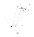
- reflected light output after the input micromirror reflects incident light has a particular movable range on the plane on which the output micromirror array 140 is located.
- the maximum movable ranges of the reflected light that is output after all the input micromirrors reflect the incident light with the same incident angle have no common intersection on the plane on which the output micromirror array 140 is located, that is, on the plane on which the output micromirror array 140 is located, there is no region that can be located simultaneously within the maximum movable ranges of the reflected light output by all the input micromirrors.
- full cross-connect refers to that an optical signal input through any input port can be output through any output port of the optical switch, that is, each input micromirror in the input micromirror array can reflect the incident light with the same incident angle onto any output micromirror in the output micromirror array.
- the maximum movable ranges of the reflected light that is output after all the input micromirrors reflect the incident light with the same incident angle may have a common intersection on the plane on which the output micromirror array 140 is located, but an area of the common intersection is less than the area of the reflection region of the output micromirror array 140 .
- the input micromirror array 130 includes input micromirrors 131 and 132 . Because the input micromirrors 131 and 132 can be deflected in two mutually perpendicular directions, reflected light output after the input micromirrors 131 and 132 reflect incident light has particular movable ranges on the plane on which the output micromirror array 140 is located, as shown by S 1 and S 2 in FIG. 3 respectively, where S 3 is an intersection of S 1 and S 2 .
- maximum movable ranges of reflected light that is output by all input micromirrors have no common intersection or same intersection on a plane on which an output micromirror array is located; or even though there is a common intersection, an area of the common intersection is less than an area of a reflection region of the output micromirror array.
- the optical switch is designed as that maximum movable ranges of reflected light that is output after all input micromirrors reflect incident light with a same incident angle have no common intersection on a plane on which an output micromirror array is located; or maximum movable ranges of reflected light that is output after all input micromirrors reflect incident light with a same incident angle have a common intersection on a plane on which an output micromirror array is located, and an area of the common intersection is less than an area of a reflection region of the output micromirror array, which can implement a large-scale array, and therefore can meet a requirement of a switching node for a throughput capacity.
- the input micromirror array 130 includes N input micromirror subarrays
- the output micromirror array 140 includes N output micromirror subarrays
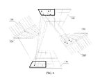
- the input micromirror array 130 includes 6 input micromirror subarrays, and each input micromirror subarray may include, for example, 4 input micromirrors; the output micromirror array 140 includes 6 output micromirror subarrays, and each output micromirror subarray may also include, for example, 4 output micromirrors.
- Each input micromirror in the i th input micromirror subarray can reflect the optical signal onto any output micromirror of 4 output micromirrors included in the i th output micromirror subarray, as shown by solid lines and dashed lines in FIG. 4 .
- the micromirror subarray pair internally has a full cross-connect feature. That is, each input micromirror in the micromirror subarray pair can reflect the optical signal onto any output micromirror in the micromirror subarray pair.
- maximum movable ranges of reflected light that is output after all input micromirrors in the micromirror subarray pair reflect incident light with a same incident angle have a common intersection on a plane on which output micromirrors in the micromirror subarray pair are located, and an area of the common intersection is greater than or equal to areas of reflection regions of all the output micromirrors.
- the input port array 110 may include N input port subarrays
- the input collimator array 120 may include N input collimator subarrays
- the output collimator array 150 may include N output collimator subarrays
- the output port array 160 may also include N output port subarrays, where there is a one-to-one correspondence between the N input micromirror subarrays and the N input collimator subarrays, and between the N input micromirror subarrays and the N input port subarrays, and there is also a one-to-one correspondence between the N output micromirror subarrays and the N output collimator subarrays, and between the N output micromirror subarrays and the N output port subarrays.
- this embodiment of the present invention is not limited thereto.
- the j th input micromirror subarray of the input micromirror array 130 includes an input adjacent region, and an input micromirror in the input adjacent region can reflect the optical signal onto an output micromirror in the k th output micromirror subarray, where the k th output micromirror subarray is adjacent to the j th output micromirror subarray, j and k are natural numbers, and j and k are less than or equal to N.
- one or more input micromirror subarrays of the input micromirror array 130 have an input adjacent region.
- An input micromirror in the input adjacent region not only can reflect the optical signal onto any output micromirror in a corresponding output micromirror subarray, but also can reflect the optical signal onto an output micromirror in an output micromirror subarray adjacent to the corresponding output micromirror subarray.
- the j th input micromirror subarray may be one or more particular input micromirror subarrays of the input micromirror array 130 , or may be any input micromirror subarray of the input micromirror array 130 .
- This embodiment of the present invention is not limited thereto.
- the input adjacent region included in the j th input micromirror subarray is close to the k th input micromirror subarray, and the input adjacent region may be a part or all of reflection regions of one or more input micromirrors included in the j th input micromirror subarray.
- This embodiment of the present invention is not limited thereto.
- an optical signal is first input to an input collimator array via an input port array, and the optical signal passing through the input collimator array arrives at an input micromirror array, where an input micromirror, corresponding to each input beam, in the input micromirror array can reflect the beam onto different micromirrors in an output micromirror array by means of deflection by a different angle; a corresponding micromirror in the output micromirror array can further reflect, by means of deflection, the beam onto an output collimator array corresponding to the output micromirror array; and after performing beam conversion, the output collimator array couples the beam to a corresponding output port array, thereby completing a scheduling function of an optical switch.
- an optical signal that enters the optical switch through each input port and input collimator can be incident only on an input micromirror corresponding to the input port and the input collimator; similarly, each optical signal reflected by an output micromirror can enter only an output collimator corresponding to the output micromirror and be output through a corresponding output port.
- the optical switch according to this embodiment of the present invention may include: N input port subarrays, N output port subarrays, N input collimator subarrays, N input micromirror subarrays, N output micromirror subarrays, and N output collimator subarrays, where there is a one-to-one correspondence between the N input micromirror subarrays and the N input collimator subarrays, and between the N input micromirror subarrays and the N input port subarrays, and there is also a one-to-one correspondence between the N output micromirror subarrays and the N output collimator subarrays, and between the N output micromirror subarrays and the N output port subarrays.
- each input micromirror in the i th input micromirror subarray can reflect an optical signal incident via an input collimator subarray onto any output micromirror in the corresponding i th output micromirror subarray; similarly, any output micromirror in the i th output micromirror subarray can reflect a beam, reflected by the output micromirror, onto the corresponding i th output collimator subarray by means of deflection by a different angle, so that the beam is output through a corresponding output port in the corresponding i th output port subarray.
- an optical signal entered through any input port in the i th input port subarray can be output through any output port in the i th output port subarray, as shown by solid lines and dashed lines in FIG. 4 , or as shown by solid lines in FIG. 5 .
- an input micromirror in the input adjacent region can reflect an optical signal onto an output micromirror in the k th output micromirror subarray, and after passing through the k th output collimator subarray, the optical signal is output through an output port in the k th output port subarray. Therefore, optical signals entered through some input ports in the j th input port subarray can be output through some output ports in the k th output port subarray, as shown by dashed lines in FIG. 5 .
- the quantities of devices included in all the subarrays may also be not equal, for example, a quantity of input micromirrors included in an input micromirror subarray may be not equal to a quantity of output micromirrors included in an output micromirror subarray.
- the optical switch is designed as that maximum movable ranges of reflected light that is output after all input micromirrors reflect incident light with a same incident angle have no common intersection on a plane on which an output micromirror array is located; or maximum movable ranges of reflected light that is output after all input micromirrors reflect incident light with a same incident angle have a common intersection on a plane on which an output micromirror array is located, and an area of the common intersection is less than an area of a reflection region of the output micromirror array, which can implement a large-scale array, and therefore can meet a requirement of a switching node for a throughput capacity.
- a first input port included in the input port array 110 is connected to a first output port included in the output port array 160 by using a fiber 170 , so that the optical signal input through a second input port included in the input port array 110 can be output through any second output port included in the output port array 160 .
- full cross-connect can be implemented for an optical signal, that is, an optical signal entered through each input port in an input port subarray can be output through any output port in a corresponding output port subarray.
- full cross-connect cannot be implemented for an optical signal.
- some input ports and some output ports may be connected by using fibers, and then a feature that optical signals entered through some input ports in an input port subarray can be output through some output ports in an output port subarray adjacent to a corresponding output port subarray is used, so that full cross-connect can be implemented for an optical signal between the input ports and the output ports of the entire optical switch, that is, an optical signal input through any second input port of the optical switch can be output through any second output port of the optical switch.
- the first input port indicates an input port that is in the input port array and connected to an output port by using a fiber
- the first output port indicates an output port that is in the output port array and connected to an input port by using a fiber
- the second input port indicates an input port that is in the input port array and not connected to an output port by using a fiber, that is, an input port in the input port array except the first input port
- the second output port indicates an output port that is in the output port array and not connected to an input port by using a fiber, that is, an output port in the output port array except the first output port.
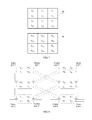
- N is 6; the i th input micromirror subarray I i includes two input micromirror regions I i,1 and I i,2 ; the i th output micromirror subarray O i includes two output micromirror regions O i,1 and O i,2 ; each input micromirror in the input micromirror region I 1,2 can reflect the optical signal onto each output micromirror in the output micromirror region O 2,1 ; each input micromirror in I 2,1 adjacent to the input micromirror region I 1,2 can reflect the optical signal onto each output micromirror in O 1,2 adjacent to the output micromirror region O 2,1 ; each input micromirror in the input micromirror region I 3,2 can reflect the optical signal onto each output micromirror in the output micromirror region O 4,1 ; each input micromirror in I 4,1 adjacent to the input micromirror region I 3,2
- each input micromirror in the input micromirror region I 1,2 can reflect the optical signal onto each output micromirror in the output micromirror region O 2,1 ; each input micromirror in the input micromirror regions I 2,1 , I 3,2 , and I 4,1 can reflect the optical signal onto each output micromirror in the output micromirror regions O 1,2 , O 4,1 , and O 3,2 ; and a connection relationship between each first input port and each first output port is shown in FIG. 8 .
- input ports corresponding to the input micromirror regions I 1,2 , I 2,1 , I 3,2 , and I 4,1 are second input ports that are reserved for receiving an externally input optical signal;
- output ports corresponding to the output micromirror regions O 2,1 , O 1,2 , O 4,1 , and O 3,2 are second output ports that are reserved for outputting an optical signal to the outside.
- the first input ports corresponding to the input micromirror regions I 1,1 , I 2,2 , I 3,1 , I 4,2 , I 5,1 , I 5,2 , I 6,1 , and I 6,2 , and the first output ports corresponding to the output micromirror regions O 5,1 , O 5,2 , O 6,1 , O 6,2 , O 3,1 , O 4,2 , O 1,1 , and O 2,2 correspond in a one-to-one manner, and are connected by using fibers.
- input ports corresponding to the input micromirror region I 1,1 and output ports corresponding to the output micromirror region O 5,1 correspond in a one-to-one manner, and are connected by using fibers.
- input ports corresponding to the input micromirror region I 3,1 and output ports corresponding to the output micromirror region O 6,1 correspond in a one-to-one manner, and are connected by using fibers.
- the first input ports include input ports corresponding to the input micromirror regions I 1,1 , I 2,2 , I 3,1 , I 4,2 , I 5,1 , I 5,2 , I 6,1 , and I 6,2 ; similarly, the first output ports include output ports corresponding to the output micromirror regions O 5,1 , O 5,2 , O 6,1 , O 6,2 , O 3,1 , O 4,2 , O 1,1 , and O 2,2 .
- an optical signal input through any input port of the second input ports can be output through any second output port of the optical switch.
- a path for transmitting an optical signal between input ports and output ports may be shown in the following Table 1.
- the symbol “ ⁇ ” indicates a path of transmitting, in space, an optical signal from an input micromirror to an output micromirror, and the symbol “ ⁇ ” indicates a path of transmitting the optical signal in a fiber.
- optical signals may be input through the input port 1 , the input port 2 , the input port 3 , and the input port 4 , and be output through the output port 1 , the output port 2 , the output port 3 , and the output port 4 respectively.
- each input micromirror in the input micromirror regions I 1,2 , I 2,1 , I 3,2 , and I 4,1 can reflect the optical signal onto each output micromirror in the output micromirror regions O 2,1 , O 1,2 , O 4,1 , and O 3,2 . Therefore, the optical signals may be input through the input port 1 , the input port 2 , the input port 3 , and the input port 4 , and be output through the output port 2 , the output port 1 , the output port 4 , and the output port 3 respectively.
- the input optical signal can arrive at the output micromirror region O 3,1 by means of deflection of an input micromirror, that is, by means of transmission on an internal space path. Then the optical signal can arrive at the input micromirror region I 5,1 through an external fiber, that is, by means of transmission on an external fiber path.
- the optical signal can arrive at the output micromirror region O 5,1 from the input micromirror region I 5,1 by means of transmission on the internal space path. Then the optical signal can arrive at the input micromirror region I 1,1 by means of transmission on the external fiber path. Therefore, the optical signal then can be transmitted to the output micromirror region O 1,2 from the input micromirror region I 1,1 by means of transmission on the internal space path, and output through the corresponding output port 1 .
- the second input ports may also correspond to other input micromirror regions and the second output ports may also correspond to other output micromirror regions, provided that the input port 1 is adjacent to the input port 2 , and the input port 3 is adjacent to the input port 4 ; correspondingly, the output port 1 is adjacent to the output port 2 , and the output port 3 is adjacent to the output port 4 .
- the input micromirror regions I i,1 and I i,2 separately include L/2 input micromirrors
- the output micromirror regions O i,1 and O i,2 separately include L/2 output micromirrors, where L is an even number.
- a reflection area of an input micromirror region or an output micromirror region may be half of a reflection area of an entire input micromirror subarray or output micromirror subarray, but the present invention is not limited thereto.
- a ratio of the reflection area of the input micromirror region or the output micromirror region to the reflection area of the entire input micromirror subarray or output micromirror subarray may be another value such as 2 ⁇ 5 or 1 ⁇ 3.
- each input micromirror subarray includes M input micromirrors
- each output micromirror subarray includes M output micromirrors, where M is a natural number. That is, a quantity of input micromirrors included in each input micromirror subarray is equal to a quantity of output micromirrors included in each output micromirror subarray.
- a quantity of input micromirrors included in an input micromirror subarray may be equal to a quantity of output micromirrors included in a corresponding output micromirror subarray, but quantities of input micromirrors included in different input micromirror subarrays may not be equal.
- the quantity of input micromirrors included in each input micromirror subarray is not equal to the quantity of output micromirrors included in each output micromirror subarray.
- the optical switch includes 6 input micromirror subarrays and 6 corresponding output micromirror subarrays. It is assumed that each input micromirror subarray includes two input micromirrors, and each output micromirror subarray includes two output micromirrors, that is, each input micromirror region and each output micromirror region includes one input micromirror and one output micromirror respectively. Therefore, as shown in FIG.
- the optical switch includes 4 input ports, that is, input ports corresponding to input micromirrors that are included in the input micromirror regions I 1,2 , I 2,1 , I 3,2 , and I 4,1 respectively; the optical switch further includes 4 output ports, that is, output ports corresponding to output micromirrors that are included in the output micromirror regions O 2,1 , O 1,2 , O 4,1 , and O 3,2 respectively.
- a 4*4 optical switch may be constructed by using 6 2*2 optical switches, where a total quantity of input ports or output ports of the optical switch is 12 (that is, 4*3).
- a 4*4 optical switch is constructed according to a completely nonblocking CLOS structure, 2 2*3 optical switches, 3 2*2 optical switches, and 2 3*2 optical switches are required.
- a total quantity of input ports or output ports of the optical switch in the CLOS structure is 16 (4*4). Therefore, a structure of the optical switch according to this embodiment of the present invention is superior to another purely-mathematical topological structure, and has higher port utilization, that is, relatively few ports may be used to implement expansion of the optical switch.
- M is 320
- that is, an example of constructing a 640*640 optical switch by using a 320*320 optical switch is used for description
- 640 2*3 optical switches and 3 320*320 optical switches are required, that is, a total quantity of input ports or output ports of the constructed optical switch in the CLOS structure is 640*4; if the optical switch in this embodiment of the present invention is used, a total quantity of input ports or output ports of the optical switch is 640*3. Therefore, the optical switch according to this embodiment of the present invention has higher port utilization.
- optical switch constructed according to this embodiment of the present invention can also have completely nonblocking and full cross-connect features, and may be applied to a scenario in which a large-scale optical switch is required, such as a backbone network switching node or a data center.
- the optical switch is designed as that maximum movable ranges of reflected light that is output after all input micromirrors reflect incident light with a same incident angle have no common intersection on a plane on which an output micromirror array is located; or maximum movable ranges of reflected light that is output after all input micromirrors reflect incident light with a same incident angle have a common intersection on a plane on which an output micromirror array is located, and an area of the common intersection is less than an area of a reflection region of the output micromirror array, which can implement a large-scale array, and therefore can meet a requirement of a switching node for a throughput capacity.
- the optical switch in this embodiment of the present invention further has relatively high port utilization, that is, relatively few ports may be used to implement expansion of the optical switch; therefore, the optical switch may be applied to a scenario in which a large-scale optical switch is required, such as a backbone network switching node or a data center.
- the i th input micromirror subarray including M input micromirrors and the i th output micromirror subarray including M output micromirrors form the i th micromirror subarray pair
- Each first micromirror subarray pair corresponds to S input ports in the input port array and 2S ⁇ 1 output ports in the output port array
- each second micromirror subarray pair corresponds to R input ports in the input port array and R output ports in the output port array
- each third micromirror subarray pair corresponds to 2S ⁇ 1 input ports in the input port array and S output ports in the output port array.
- the y th output port O 1 x,y corresponding to the x th first micromirror subarray pair and the x th input port I 2 y,x corresponding to the y th second micromirror subarray pair are connected by using a fiber
- the input micromirror array 130 includes N input micromirror subarrays
- the output micromirror array 140 includes N output micromirror subarrays
- a micromirror subarray pair internally has a full cross-connect feature, that is, each input micromirror in the micromirror subarray pair can reflect the optical signal onto any output micromirror in the micromirror subarray pair.
- FIG. 10 a connection relationship of ports among the first micromirror subarray pair, the second micromirror subarray pair, and the third micromirror subarray pair may be shown in FIG. 10 .
- a connection between an input port and an output port or a connection between an output port and an input port may be implemented by using an external fiber 170 , as shown by solid lines between ports in FIG. 10 , but this embodiment of the present invention is not limited thereto.
- a large-scale, nonblocking, and fully cross-connected optical switch may be constructed and applied to a backbone network node or a data center.
- a 25*25 optical switch may be produced according to a 3D-MEMS technological level.
- a larger-scale and locally cross-connected optical switch may be produced, where 25 13*25 fully cross-connected port groups, 25 25*13 fully cross-connected port groups, and 25 25*25 fully cross-connected port groups are included.
- a fully cross-connected optical switch with scale of 325*325 may be formed. Therefore, in the solution, constructing a topological structure by using a locally cross-connected optical switch features higher integration and a smaller volume compared with constructing a topological structure by using an independent small-scale optical switch.
- cross scheduling time of a switching node is an important indicator in a WDM system.
- cross scheduling time mainly depends on switching time of the optical switch, and the switching time of the optical switch is related to a deflection angle of a micromirror in a switching process.
- full cross-connect is required to be implemented only inside a micromirror subarray pair, and it is unnecessary to implement full cross-connect of all ports within a range of the entire optical switch. Therefore, a deflection angle of a micromirror is less than that of a fully cross-connected optical switch of equivalent scale, and therefore switching time is shorter. Therefore, according to a switching node constructed by using a large-scale optical switch that is constructed according to this embodiment of the present invention, cross scheduling time is shorter.
- the optical switch is designed as that maximum movable ranges of reflected light that is output after all input micromirrors reflect incident light with a same incident angle have no common intersection on a plane on which an output micromirror array is located; or maximum movable ranges of reflected light that is output after all input micromirrors reflect incident light with a same incident angle have a common intersection on a plane on which an output micromirror array is located, and an area of the common intersection is less than an area of a reflection region of the output micromirror array, which can implement a large-scale array, and therefore can meet a requirement of a switching node for a throughput capacity.
- the optical switch according to this embodiment of the present invention further has characteristics of higher integration, a small volume, and short switching time.
- the optical switch includes: an input port array, an input collimator array connected to the input port array, an input micromirror array, an output micromirror array, an output collimator array, and an output port array connected to the output collimator array.
- the input collimator array is configured to perform collimation and beam expansion on an optical signal input through the input port array, and make the optical signal, on which collimation and beam expansion have been performed, be incident on the input micromirror array.
- the input micromirror array is configured to reflect the optical signal, output by the input collimator array, onto the output micromirror array.
- the output micromirror array is configured to reflect the optical signal, reflected by the input micromirror array, onto the output collimator array.
- the output collimator array is configured to couple the optical signal, reflected by the output micromirror array, to the output port array.
- All input micromirrors included in the input micromirror array can be deflected in two mutually perpendicular directions, and maximum movable ranges of reflected light that is output after all the input micromirrors reflect incident light with a same incident angle have no common intersection on a plane on which the output micromirror array is located; or maximum movable ranges of reflected light that is output after all the input micromirrors reflect incident light with a same incident angle have a common intersection on a plane on which the output micromirror array is located, and an area of the common intersection is less than an area of a reflection region of the output micromirror array.
- the input micromirror array includes N input micromirror subarrays
- the output micromirror array includes N output micromirror subarrays
- the input port array 110 includes N input port subarrays
- the input collimator array 120 includes N input collimator subarrays
- the output port array 160 includes N output port subarrays
- the output collimator array 150 includes N output collimator subarrays, where each input port subarray corresponds to one input collimator subarray and one input micromirror subarray, and each output port subarray corresponds to one output collimator subarray and one output micromirror subarray.
- the input micromirror included in the input micromirror array and the output micromirror included in the output micromirror array are micro-electro-mechanical system MEMS micromirrors.
- the wavelength-combined optical signal includes at least two wavelengths.
- an optical switch included in the wavelength division multiplexing optical system is designed to include at least a first input micromirror subarray, a second input micromirror subarray, a third output micromirror subarray, and a fourth output micromirror subarray.
- Incident light can be incident within a reflection region of the third output micromirror subarray after being reflected by the first input micromirror subarray, and the incident light cannot be incident within a reflection region of the fourth output micromirror subarray after being reflected by the first input micromirror subarray.
- Incident light can be incident within the reflection region of the fourth output micromirror subarray after being reflected by the second input micromirror subarray. This can implement a large-scale array, and therefore can meet a requirement of a switching node for a throughput capacity.
- this embodiment of the present invention is not limited thereto, and the quantities of the DEMUXes and the MUXes may also be different, for example, m1>m2, or m2>m1.
- an m-dimension and N-wavelength switching node in the WDM system is used as an example, as shown in FIG. 11 .
- the input port array of the optical switch according to this embodiment of the present invention is divided into N input port subarrays, and a quantity of input ports included in each input port subarray is M; likewise, the output port array may be divided into N output port subarrays, and a quantity of output ports included in each output port subarray is M, where M is greater than or equal to m. Specially, if there is a local add/drop wavelength, the port quantity M is greater than m.
- an optical path connection may be established between any input port in each group and any output port in the group, that is, full cross-connect can be implemented for input and output ports in each group.
- some ports may also be scheduled to an adjacent group and some output ports in the adjacent group are used for output.
- WDM light from m dimensions is divided into N different wavelengths by using the DEMUXes.
- ⁇ 1 of all the dimensions is respectively connected to input ports in the first input port subarray, so as to serve as the first wavelength-combined optical signal;
- ⁇ 2 of all the dimensions is respectively connected to input ports in the second input port subarray, so as to serve as the second wavelength-combined optical signal;
- other wavelengths of each dimension are successively connected to input ports in each input port subarray in such a manner.
- all ⁇ i from the m dimensions is connected to the i th input port subarray of the optical switch.
- An input port, of each MUX, for inputting ⁇ 1 is connected to an output port in the first output port subarray of the optical switch; an input port, of each MUX, for inputting ⁇ 2 is connected to an output port in the second output port subarray of the optical switch.
- an input port, of each MUX, for inputting the i th wavelength-combined optical signal is connected to an output port in the i th output port subarray of the optical switch. Therefore, single-wavelength light output through output ports of the optical switch and destined for a same dimension is multiplexed into a fiber of the corresponding dimension by a MUX corresponding to the dimension, and is transmitted to a next switching node. If there are extra input/output ports in each input/output port subarray, these extra input ports are used for adding a local wavelength, and the extra output ports are used for dropping a local wavelength.
- a WDM signal from the dimension a is first demultiplexed as single-wavelength light by a DEMUX corresponding to the dimension a, and light ⁇ c of the c th wavelength is sent to an input port in the c th input port subarray of a locally cross-connected optical switch.
- an optical path connection is established between the a th input port in the c th group and the b th output port in the c th group, and in this way, ⁇ c from the dimension a is sent to an output port corresponding to the dimension b in the c th output port subarray, where a, b, and c are natural numbers, a and b are less than or equal to m, and c is less than or equal to N.
- a MUX corresponding to the dimension b multiplexes ⁇ c output by the optical switch and other single-wavelength signals that need to be destined for the dimension b, and then outputs a multiplexed signal.
- wavelength scheduling is complete.
- the optical signal output after the multiplexing is sent to a corresponding single fiber, so as to be transmitted to a next switching node. In this way, wavelength-level scheduling between dimensions is complete on a current switching node.
- ⁇ c When a local wavelength ⁇ c needs to be destined for a dimension a, ⁇ c is first sent to the optical switch by using an input port, reserved for adding, in the c th input port subarray of the optical switch, and then ⁇ c is sent to an output port corresponding to the dimension a in the c th output port subarray by means of scheduling between input and output ports in the c th group.
- a MUX corresponding to the dimension a multiplexes ⁇ c and other single-wavelength wavelengths destined for the dimension a, and sends a multiplexed signal to a fiber corresponding to the dimension a for transmission, thereby completing adding of the local wavelength.
- the input wavelength ⁇ c may be sent to an output port, reserved for dropping, in the c th output port subarray by means of scheduling between input and output ports in the c th group, thereby completing dropping of a local wavelength.
- the wavelength-combined optical signal includes at least two wavelengths.
- the wavelength-combined optical signal includes two or more wavelengths.
- each group of input and output ports only completes scheduling of one wavelength.
- two-wavelength optical signals or multi-wavelength optical signals may also be scheduled in a same group.
- a port quantity in each group of ports should be greater than or equal to 2m or N*m.
- the wavelength-combined optical signal may also include only one wavelength, and the present invention is not limited thereto.
- description is provided only by using 2 ⁇ m as an example, but the present invention is not limited thereto, For example, a value of m may also be 1.
- the input micromirror included in the input micromirror array 130 and the output micromirror included in the output micromirror array 140 are micro-electro-mechanical system MEMS micromirrors.
- the present invention is not limited thereto.
- the input micromirror and the output micromirror according to this embodiment of the present invention may also be piezoceramics-based micromirrors, or the like.
- a switching node accommodating 80 wavelengths of 8 dimensions and reserving 50% add/drop wavelengths is used as an example.
- a 960 ⁇ 960 optical switch is required.
- an optical switch with maximum scale in the industry is produced based on a 3D-MEMS technology.
- the 960 ⁇ 960 optical switch cannot be implemented.
- a structure of a locally cross-connected optical switch according to an embodiment of the present invention is used to produce such a 960*960 optical switch, a requirement can be satisfied if there are 12 input ports and 12 output ports in each group of fully cross-connected ports.
- Requirements of such a locally cross-connected optical switch and a 12 ⁇ 12 3D-MEMS optical switch for the 3D-MEMS technology are basically equivalent, and many device manufacturers in the industry have such a technology.
- the j th input micromirror subarray of the input micromirror array includes an input adjacent region, and an input micromirror in the input adjacent region can reflect the optical signal onto an output micromirror in the k th output micromirror subarray, where the k th output micromirror subarray is adjacent to the j th output micromirror subarray, j and k are natural numbers, and j and k are less than or equal to N.
- a first input port included in the input port array is connected, by using a fiber, to a first output port included in the output port array, so that the optical signal input through a second input port included in the input port array can be output through any second output port included in the output port array.
- N is 6; the i th input micromirror subarray I i includes two input micromirror regions I i,1 and I i,2 ; the i th output micromirror subarray O i includes two output micromirror regions O i,1 and O i,2 ; each input micromirror in the input micromirror region I 1,2 can reflect the optical signal onto each output micromirror in the output micromirror region O 2,1 ; each input micromirror in I 2,1 adjacent to the input micromirror region I 1,2 can reflect the optical signal onto each output micromirror in O 1,2 adjacent to the output micromirror region O 2,1 ; each input micromirror in the input micromirror region I 3,2 can reflect the optical signal onto each output micromirror in the output micromirror region O 4,1 ; each input micromirror in I 4,1 adjacent to the input micromirror region I 3,2 can reflect the optical signal onto each output
- the input micromirror regions I i,1 and I i,2 separately include L/2 input micromirrors
- the output micromirror regions O i,1 and O i,2 separately include L/2 output micromirrors, where L is an even number.
- each input micromirror subarray includes M input micromirrors
- each output micromirror subarray includes M output micromirrors, where M is a natural number.
- the i th input micromirror subarray including M input micromirrors and the i th output micromirror subarray including M output micromirrors form the i th micromirror subarray pair
- Each first micromirror subarray pair corresponds to S input ports in the input port array and 2S ⁇ 1 output ports in the output port array
- each second micromirror subarray pair corresponds to R input ports in the input port array and R output ports in the output port array
- each third micromirror subarray pair corresponds to 2S ⁇ 1 input ports in the input port array and S output ports in the output port array.
- the y th output port O 1 x,y corresponding to the x th first micromirror subarray pair and the x th input port I 2 y,x corresponding to the y th second micromirror subarray pair are connected by using a fiber
- an optical switch included in the wavelength division multiplexing optical system is designed to include at least a first input micromirror subarray, a second input micromirror subarray, a third output micromirror subarray, and a fourth output micromirror subarray.
- Incident light can be incident within a reflection region of the third output micromirror subarray after being reflected by the first input micromirror subarray, and the incident light cannot be incident within a reflection region of the fourth output micromirror subarray after being reflected by the first input micromirror subarray.
- Incident light can be incident within the reflection region of the fourth output micromirror subarray after being reflected by the second input micromirror subarray. This can implement a large-scale array, and therefore can meet a requirement of a switching node for a throughput capacity.
- an embodiment of the present invention provides an optical switch.
- the optical switch includes: an input port array, an input collimator array connected to the input port array, an input micromirror array, an output micromirror array, an output collimator array, and an output port array connected to the output collimator array.
- the input collimator array is configured to perform collimation and beam expansion on an optical signal input through the input port array, and make the optical signal, on which collimation and beam expansion have been performed, be incident on the input micromirror array.
- the input micromirror array is configured to reflect the optical signal, output by the input collimator array, onto the output micromirror array.
- the output micromirror array is configured to reflect the optical signal, reflected by the input micromirror array, onto the output collimator array.
- the output collimator array is configured to couple the optical signal, reflected by the output micromirror array, to the output port array.
- the input micromirror array includes at least a first input micromirror subarray and a second input micromirror subarray
- the output micromirror array includes at least a third output micromirror subarray and a fourth output micromirror subarray.
- Incident light can be incident within a reflection region of the third output micromirror subarray after being reflected by the first input micromirror subarray, and the incident light cannot be incident within a reflection region of the fourth output micromirror subarray after being reflected by the first input micromirror subarray.
- Incident light can be incident within the reflection region of the fourth output micromirror subarray after being reflected by the second input micromirror subarray.
- the input micromirror array includes N input micromirror subarrays
- the output micromirror array includes N output micromirror subarrays
- each input micromirror in the first input micromirror subarray can reflect incident light onto each output micromirror in the third output micromirror subarray; each input micromirror in the second input micromirror subarray can reflect incident light onto each output micromirror in the fourth output micromirror subarray.
- each input micromirror in the first input micromirror subarray cannot reflect incident light onto any output micromirror in the fourth output micromirror subarray.
- the first input micromirror subarray is configured to reflect incident light, incident on any input micromirror in the first input micromirror subarray, onto any output micromirror in the third output micromirror subarray, but not configured to reflect the incident light onto any output micromirror in the fourth output micromirror subarray.
- the second input micromirror subarray is configured to reflect incident light, incident on any input micromirror in the second input micromirror subarray, onto any output micromirror in the fourth output micromirror subarray.
- the optical switch is designed to include at least a first input micromirror subarray, a second input micromirror subarray, a third output micromirror subarray, and a fourth output micromirror subarray.
- Incident light can be incident within a reflection region of the third output micromirror subarray after being reflected by the first input micromirror subarray, and the incident light cannot be incident within a reflection region of the fourth output micromirror subarray after being reflected by the first input micromirror subarray.
- Incident light can be incident within the reflection region of the fourth output micromirror subarray after being reflected by the second input micromirror subarray. This can implement a large-scale array, and therefore can meet a requirement of a switching node for a throughput capacity.
- the output micromirror array further includes a fifth output micromirror subarray, and the incident light can also be incident within a reflection region of the fifth output micromirror subarray after being reflected by the first input micromirror subarray, where the third output micromirror subarray and the fifth output micromirror subarray are adjacent micromirror arrays.
- the output micromirror array may further include the fifth output micromirror subarray adjacent to the third output micromirror subarray
- the input micromirror array may further include a sixth input micromirror subarray.
- the first input micromirror subarray corresponds to the third output micromirror subarray
- the second input micromirror subarray corresponds to the fourth output micromirror subarray
- the fifth output micromirror subarray corresponds to the sixth input micromirror subarray. That is, each input micromirror in the sixth input micromirror subarray can reflect incident light onto each output micromirror in the fifth output micromirror subarray.
- Each input micromirror in the first input micromirror subarray can further reflect incident light onto each output micromirror in the fifth output micromirror subarray.
- the first input micromirror subarray is configured to reflect incident light, incident on any input micromirror in the first input micromirror subarray, onto any output micromirror in the third or fifth output micromirror subarray, where the third output micromirror subarray and the fifth output micromirror subarray are adjacent micromirror arrays.
- a first input port included in the input port array is connected, by using a fiber, to a first output port included in the output port array, so that the optical signal input through a second input port included in the input port array can be output through any second output port included in the output port array.
- the first input port indicates an input port that is in the input port array and connected to an output port by using a fiber
- the first output port indicates an output port that is in the output port array and connected to an input port by using a fiber
- the second input port indicates an input port that is in the input port array and not connected to an output port by using a fiber, that is, an input port in the input port array except the first input port
- the second output port indicates an output port that is in the output port array and not connected to an input port by using a fiber, that is, an output port in the output port array except the first output port.
- the input micromirror array includes N input micromirror subarrays, and the i th input micromirror subarray of the N input micromirror subarrays includes two input micromirror subregions I i,1 and I i,2 ;
- the output micromirror array includes N output micromirror subarrays, and the i th output micromirror subarray of the N output micromirror subarrays includes two output micromirror subregions O i,1 and O i,2 ; each input micromirror in the input micromirror subregion I 42 can reflect the optical signal onto each output micromirror in the output micromirror subregion O 2,1 ; each input micromirror in I 2,1 adjacent to the input micromirror subregion I 1,2 can reflect the optical signal onto each output micromirror in O 1,2 adjacent to the output micromirror subregion O 2,1 ; each input micromirror in the input micromir
- the input micromirror subregions I i,1 and I i,2 separately include L/2 input micromirrors
- the output micromirror subregions O i,1 and O i,2 separately include L/2 output micromirrors, where L is an even number.
- each input micromirror subarray includes M input micromirrors
- each output micromirror subarray includes M output micromirrors, where M is a natural number.
- the optical switch is designed to include at least a first input micromirror subarray, a second input micromirror subarray, a third output micromirror subarray, and a fourth output micromirror subarray.
- Incident light can be incident within a reflection region of the third output micromirror subarray after being reflected by the first input micromirror subarray, and the incident light cannot be incident within a reflection region of the fourth output micromirror subarray after being reflected by the first input micromirror subarray.
- Incident light can be incident within the reflection region of the fourth output micromirror subarray after being reflected by the second input micromirror subarray.
- the optical switch in this embodiment of the present invention further has relatively high port utilization, that is, relatively few ports may be used to implement expansion of the optical switch; therefore, the optical switch may be applied to a scenario in which a large-scale optical switch is required, such as a backbone network switching node or a data center.
- the i th input micromirror subarray including M input micromirrors and the i th output micromirror subarray including M output micromirrors form the i th micromirror subarray pair
- Each first micromirror subarray pair corresponds to S input ports in the input port array and 2S ⁇ 1 output ports in the output port array
- each second micromirror subarray pair corresponds to R input ports in the input port array and R output ports in the output port array
- each third micromirror subarray pair corresponds to 2S ⁇ 1 input ports in the input port array and S output ports in the output port array.
- the y th output port O 1 x,y corresponding to the x th first micromirror subarray pair and the x th input port I 2 y,x corresponding to the y th second micromirror subarray pair are connected by using a fiber
- the input micromirror included in the input micromirror array and the output micromirror included in the output micromirror array are micro-electro-mechanical system MEMS micromirrors.
- cross scheduling time of a switching node is an important indicator in a WDM system.
- cross scheduling time mainly depends on switching time of the optical switch, and the switching time of the optical switch is related to a deflection angle of a micromirror in a switching process.
- full cross-connect is required to be implemented only inside a micromirror subarray pair, and it is unnecessary to implement full cross-connect of all ports within a range of the entire optical switch. Therefore, a deflection angle of a micromirror is less than that of a fully cross-connected optical switch of equivalent scale, and therefore switching time is shorter. Therefore, according to a switching node constructed by using a large-scale optical switch that is constructed according to this embodiment of the present invention, cross scheduling time is shorter.
- the optical switch is designed to include at least a first input micromirror subarray, a second input micromirror subarray, a third output micromirror subarray, and a fourth output micromirror subarray.
- Incident light can be incident within a reflection region of the third output micromirror subarray after being reflected by the first input micromirror subarray, and the incident light cannot be incident within a reflection region of the fourth output micromirror subarray after being reflected by the first input micromirror subarray.
- Incident light can be incident within the reflection region of the fourth output micromirror subarray after being reflected by the second input micromirror subarray.
- This can implement a large-scale array, and therefore can meet a requirement of a switching node for a throughput capacity.
- the optical switch according to this embodiment of the present invention further has characteristics of higher integration, a small volume, and short switching time.
- An embodiment of the present invention further provides a wavelength division multiplexing optical system.
- the wavelength division multiplexing optical system includes the optical switch according to the foregoing embodiment of the present invention, m1 demultiplexers DEMUXes, and m2 multiplexers MUXes.
- the input port array includes N input port subarrays
- the input collimator array includes N input collimator subarrays
- the output port array includes N output port subarrays
- the output collimator array includes N output collimator subarrays, where each input port subarray corresponds to one input collimator subarray and one input micromirror subarray, and each output port subarray corresponds to one output collimator subarray and one output micromirror subarray.
- the optical switch includes: an input port array, an input collimator array connected to the input port array, an input micromirror array, an output micromirror array, an output collimator array, and an output port array connected to the output collimator array.
- the input collimator array is configured to perform collimation and beam expansion on an optical signal input through the input port array, and make the optical signal, on which collimation and beam expansion have been performed, be incident on the input micromirror array.
- the input micromirror array is configured to reflect the optical signal, output by the input collimator array, onto the output micromirror array.
- the output micromirror array is configured to reflect the optical signal, reflected by the input micromirror array, onto the output collimator array.
- the output collimator array is configured to couple the optical signal, reflected by the output micromirror array, to the output port array.
- the input micromirror array includes at least a first input micromirror subarray and a second input micromirror subarray
- the output micromirror array includes at least a third output micromirror subarray and a fourth output micromirror subarray.
- Incident light can be incident within a reflection region of the third output micromirror subarray after being reflected by the first input micromirror subarray, and the incident light cannot be incident within a reflection region of the fourth output micromirror subarray after being reflected by the first input micromirror subarray.
- Incident light can be incident within the reflection region of the fourth output micromirror subarray after being reflected by the second input micromirror subarray.
- the input micromirror array includes N input micromirror subarrays
- the output micromirror array includes N output micromirror subarrays
- the input micromirror included in the input micromirror array and the output micromirror included in the output micromirror array are micro-electro-mechanical system MEMS micromirrors.
- this embodiment of the present invention is not limited thereto, and the quantities of the DEMUXes and the MUXes may also be different, for example, m1>m2, or m2>m1.
- the wavelength-combined optical signal includes at least two wavelengths.
- the output micromirror array further includes a fifth output micromirror subarray, and the incident light can also be incident within a reflection region of the fifth output micromirror subarray after being reflected by the first input micromirror subarray, where the third output micromirror subarray and the fifth output micromirror subarray are adjacent micromirror arrays.
- a first input port included in the input port array is connected, by using a fiber, to a first output port included in the output port array, so that the optical signal input through a second input port included in the input port array can be output through any second output port included in the output port array.
- the input micromirror array includes N input micromirror subarrays, and the i th input micromirror subarray of the N input micromirror subarrays includes two input micromirror subregions I i,1 and I i,2 ;
- the output micromirror array includes N output micromirror subarrays, and the i th output micromirror subarray of the N output micromirror subarrays includes two output micromirror subregions O i,1 and O i,2 ; each input micromirror in the input micromirror subregion I 1,2 can reflect the optical signal onto each output micromirror in the output micromirror subregion O 2,1 ; each input micromirror in I 2,1 adjacent to the input micromirror subregion I 1,2 can reflect the optical signal onto each output micromirror in O 1,2 adjacent to the output micromirror subregion O 2,1 ; each input micromirror in the input micro
- the input micromirror subregions I i,1 and I i,2 separately include L/2 input micromirrors
- the output micromirror subregions O i,1 and O i,2 separately include L/2 output micromirrors, where L is an even number.
- each input micromirror subarray includes M input micromirrors
- each output micromirror subarray includes M output micromirrors, where M is a natural number.
- the i th input micromirror subarray including M input micromirrors and the i th output micromirror subarray including M output micromirrors form the i th micromirror subarray pair
- Each first micromirror subarray pair corresponds to S input ports in the input port array and 2S ⁇ 1 output ports in the output port array
- each second micromirror subarray pair corresponds to R input ports in the input port array and R output ports in the output port array
- each third micromirror subarray pair corresponds to 2S ⁇ 1 input ports in the input port array and S output ports in the output port array.
- the y th output port O 1 x,y corresponding to the x th first micromirror subarray pair and the x th input port I 2 y,x corresponding to the y th second micromirror subarray pair are connected by using a fiber
- optical switch included in the wavelength division multiplexing optical system may correspond to the optical switch 100 according to the embodiment of the present invention.
- features, structures, functions, and the like of some or all devices of the optical switch included in the wavelength division multiplexing optical system are the same as or similar to features, structures, and functions of corresponding devices of the optical switch 100 in the embodiment of the present invention, and are not described herein again for brevity.
- an optical switch of the wavelength division multiplexing optical system is designed to include at least a first input micromirror subarray, a second input micromirror subarray, a third output micromirror subarray, and a fourth output micromirror subarray.
- Incident light can be incident within a reflection region of the third output micromirror subarray after being reflected by the first input micromirror subarray, and the incident light cannot be incident within a reflection region of the fourth output micromirror subarray after being reflected by the first input micromirror subarray.
- Incident light can be incident within the reflection region of the fourth output micromirror subarray after being reflected by the second input micromirror subarray. This can implement a large-scale array, and therefore can meet a requirement of a switching node for a throughput capacity.
- an embodiment of the present invention further provides an optical switch array.
- the optical switch array includes multiple optical switches according to the embodiments of the present invention.
- the optical switch includes: an input port, an input collimator array connected to the input port, an input micromirror array, an output micromirror array, an output collimator array, and an output port connected to the output collimator array.
- the input collimator array is configured to perform collimation and beam expansion on an optical signal input through the input port, and make the optical signal, on which collimation and beam expansion have been performed, be incident on the input micromirror array.
- the input micromirror array is configured to reflect the optical signal, output by the input collimator array, onto the output micromirror array.
- the output micromirror array is configured to reflect the optical signal, reflected by the input micromirror array, onto the output collimator array.
- the output collimator array is configured to couple the optical signal, reflected by the output micromirror array, to the output port.
- All input micromirrors included in the input micromirror array can be deflected in two mutually perpendicular directions, and maximum movable ranges of reflected light that is output after all the input micromirrors reflect incident light with a same incident angle have no common intersection on a plane on which the output micromirror array is located; or maximum movable ranges of reflected light that is output after all the input micromirrors reflect incident light with a same incident angle have a common intersection on a plane on which the output micromirror array is located, and an area of the common intersection is less than an area of a reflection region of the output micromirror array.
- an optical switch included in the optical switch array is designed as that maximum movable ranges of reflected light that is output after all input micromirrors reflect incident light with a same incident angle have no common intersection on a plane on which an output micromirror array is located; or maximum movable ranges of reflected light that is output after all input micromirrors reflect incident light with a same incident angle have a common intersection on a plane on which an output micromirror array is located, and an area of the common intersection is less than an area of a reflection region of the output micromirror array, which can implement a large-scale array, and therefore can meet a requirement of a switching node for a throughput capacity.
- system and “network” in this specification may be often used interchangeably in this specification.
- a term “and/or” in this specification is merely used to describe an association relationship of associated objects, which means that three relationships may exist, for example, A and/or B may mean that only A exists, both A and B exist, or only B exists.
- a character “/” in this specification generally indicates an “or” relationship between contextually associated objects.
- B corresponding to A indicates that B and A are associated, and B can be determined according to A.
- determining B according to A does not mean that B is determined only according to A, and B may be alternatively determined according to A and/or other information.
- the disclosed system, apparatus, and method may be implemented in other manners.
- the described apparatus embodiment is merely exemplary.
- the unit division is merely logical function division and may be other division in actual implementation.
- a plurality of units or components may be combined or integrated into another system, or some features may be ignored or not performed.
- the displayed or discussed mutual couplings or direct couplings or communication connections may be implemented through some interfaces.
- the indirect couplings or communication connections between the apparatuses or units may be implemented in electronic, mechanical, or other forms.
- the units described as separate parts may or may not be physically separate, and parts displayed as units may or may not be physical units, may be located in one position, or may be distributed on a plurality of network units. A part or all of the units may be selected according to actual needs to achieve the objectives of the solutions of the embodiments of the present invention.
- functional units in the embodiments of the present invention may be integrated into one processing unit, or each of the units may exist alone physically, or two or more units are integrated into one unit.
- the integrated unit may be implemented in a form of hardware, or may be implemented in a form of a software functional unit.
- the integrated unit When the integrated unit is implemented in the form of a software functional unit and sold or used as an independent product, the integrated unit may be stored in a computer-readable storage medium. Based on such an understanding, the technical solutions of the present invention essentially, or the part contributing to the prior aft, or all or a part of the technical solutions may be implemented in the form of a software product.
- the software product is stored in a storage medium and includes several instructions for instructing a computer device (which may be a personal computer, a server, a network device, or the like) to perform all or a part of the steps of the methods described in the embodiments of the present invention.
- the foregoing storage medium includes: any medium that can store program code, such as a USB flash drive, a removable hard disk, a read-only memory (ROM, Read-Only Memory), a random access memory (RAM, Random Access Memory), a magnetic disk, or an optical disc.
- program code such as a USB flash drive, a removable hard disk, a read-only memory (ROM, Read-Only Memory), a random access memory (RAM, Random Access Memory), a magnetic disk, or an optical disc.
Landscapes
- Physics & Mathematics (AREA)
- General Physics & Mathematics (AREA)
- Optics & Photonics (AREA)
- Engineering & Computer Science (AREA)
- Computer Networks & Wireless Communication (AREA)
- Signal Processing (AREA)
- Mechanical Light Control Or Optical Switches (AREA)
- Use Of Switch Circuits For Exchanges And Methods Of Control Of Multiplex Exchanges (AREA)
- Optical Communication System (AREA)
Applications Claiming Priority (4)
| Application Number | Priority Date | Filing Date | Title |
|---|---|---|---|
| CN201410228121.1A CN105223657B (zh) | 2014-05-27 | 2014-05-27 | 光开关和波分复用光系统 |
| CN201410228121 | 2014-05-27 | ||
| CN201410228121.1 | 2014-05-27 | ||
| PCT/CN2014/095613 WO2015180469A1 (zh) | 2014-05-27 | 2014-12-30 | 光开关和波分复用光系统 |
Related Parent Applications (1)
| Application Number | Title | Priority Date | Filing Date |
|---|---|---|---|
| PCT/CN2014/095613 Continuation WO2015180469A1 (zh) | 2014-05-27 | 2014-12-30 | 光开关和波分复用光系统 |
Publications (2)
| Publication Number | Publication Date |
|---|---|
| US20170075074A1 US20170075074A1 (en) | 2017-03-16 |
| US10031294B2 true US10031294B2 (en) | 2018-07-24 |
Family
ID=54698029
Family Applications (1)
| Application Number | Title | Priority Date | Filing Date |
|---|---|---|---|
| US15/360,642 Expired - Fee Related US10031294B2 (en) | 2014-05-27 | 2016-11-23 | Optical switch and wavelength division multiplexing optical system |
Country Status (4)
| Country | Link |
|---|---|
| US (1) | US10031294B2 (zh) |
| EP (1) | EP3139202A4 (zh) |
| CN (1) | CN105223657B (zh) |
| WO (1) | WO2015180469A1 (zh) |
Families Citing this family (9)
| Publication number | Priority date | Publication date | Assignee | Title |
|---|---|---|---|---|
| US20170176688A1 (en) * | 2015-12-17 | 2017-06-22 | Hamid Mehrvar | Network Switch With Augmented Input and Output Capabilities |
| CN106054322B (zh) * | 2016-07-18 | 2019-04-16 | 贝耐特光学科技(昆山)有限公司 | 一种扩展波长选择开关端口数目的方法 |
| CN109725413A (zh) * | 2017-10-27 | 2019-05-07 | 华为技术有限公司 | 微镜结构及微镜阵列芯片 |
| CN111247472B (zh) * | 2017-10-30 | 2022-02-25 | 华为技术有限公司 | 一种多级mems光开关单元和光交叉装置 |
| CN109991728B (zh) * | 2017-12-29 | 2021-01-05 | 华为技术有限公司 | Mems芯片结构 |
| CN110519663B (zh) * | 2018-05-22 | 2020-11-27 | 华为技术有限公司 | 用于光开关的路径建立方法、装置及光开关 |
| CN108828712B (zh) * | 2018-06-11 | 2020-10-16 | 上海交通大学 | 基于光学相控阵的大规模集成光开关芯片 |
| CN114746792A (zh) * | 2019-11-26 | 2022-07-12 | 瑞典爱立信有限公司 | 向用户供应多层扩展现实图像 |
| CN112558288B (zh) * | 2020-11-23 | 2021-09-03 | 山东大学 | 一种基于压电驱动的时分复用多窗口叶片式快速机械光开关 |
Citations (23)
| Publication number | Priority date | Publication date | Assignee | Title |
|---|---|---|---|---|
| US5450512A (en) * | 1993-04-12 | 1995-09-12 | Matsushita Electric Industrial Co., Ltd. | Optical tap |
| US6253001B1 (en) * | 2000-01-20 | 2001-06-26 | Agilent Technologies, Inc. | Optical switches using dual axis micromirrors |
| US6330102B1 (en) * | 2000-03-24 | 2001-12-11 | Onix Microsystems | Apparatus and method for 2-dimensional steered-beam NxM optical switch using single-axis mirror arrays and relay optics |
| US6470110B1 (en) * | 2000-10-19 | 2002-10-22 | Tellium, Inc. | Monolithic integration of control elements and micro-mirror in an optical switch |
| US6560384B1 (en) * | 2000-06-01 | 2003-05-06 | Calient Networks, Inc. | Optical switch having mirrors arranged to accommodate freedom of movement |
| US20030118274A1 (en) * | 2001-12-21 | 2003-06-26 | Tetsuya Nishi | Optical cross-connect device and optical network |
| US6597825B1 (en) * | 2001-10-30 | 2003-07-22 | Calient Networks, Inc. | Optical tap for an optical switch |
| US6643425B1 (en) * | 2000-08-17 | 2003-11-04 | Calient Networks, Inc. | Optical switch having switch mirror arrays controlled by scanning beams |
| US6731833B2 (en) * | 2001-01-16 | 2004-05-04 | T-Rex Enterprises Corp. | Optical cross connect switch |
| US6766085B2 (en) * | 2001-10-01 | 2004-07-20 | Agilent Technologies, Inc. | Precisely configuring optical fibers and other optical elements using an apertured wafer positioner |
| CN1595221A (zh) | 2004-06-24 | 2005-03-16 | 北京邮电大学 | 采用洗牌Benes级间连接规则的二维微光电机械光开关及其方法 |
| US6917733B1 (en) * | 2003-04-03 | 2005-07-12 | Glimmerglass Networks, Inc. | Three-dimensional optical switch with offset input-output ports |
| US7006721B2 (en) * | 2002-04-17 | 2006-02-28 | Hitachi, Ltd. | Optical switch and beam direction module |
| CN1831574A (zh) | 2005-03-07 | 2006-09-13 | 富士通株式会社 | 波长选择开关 |
| US20080137172A1 (en) | 2006-12-06 | 2008-06-12 | Glimmerglass Networks, Inc. | Array of graduated pre-tilted mems mirrors |
| CN101263408A (zh) | 2005-08-03 | 2008-09-10 | 卡佩拉光子学公司 | Mems镜阵列的抖动幅度的自动调节方法 |
| JP2011028235A (ja) * | 2009-06-26 | 2011-02-10 | Nippon Telegr & Teleph Corp <Ntt> | 光スイッチ |
| US8125701B2 (en) * | 2006-10-11 | 2012-02-28 | Nippon Telegraph And Telephone Corporation | Optical switch |
| CN202282779U (zh) | 2011-10-27 | 2012-06-20 | 武汉光迅科技股份有限公司 | 一种光缆跳线装置 |
| US20120236216A1 (en) | 2011-03-16 | 2012-09-20 | Manish Sharma | Wavelength Selective Switch |
| CN102696194A (zh) | 2011-07-22 | 2012-09-26 | 华为技术有限公司 | 可重构的光分插复用器及波长交叉连接器 |
| CN103558668A (zh) | 2013-11-19 | 2014-02-05 | 武汉邮电科学研究院 | 波长选择开关和波长选择方法 |
| US9213142B2 (en) * | 2013-11-21 | 2015-12-15 | Huawei Technologies Co., Ltd. | Device and method for micro-electro-mechanical-system photonic switch |
-
2014
- 2014-05-27 CN CN201410228121.1A patent/CN105223657B/zh not_active Expired - Fee Related
- 2014-12-30 EP EP14892967.2A patent/EP3139202A4/en not_active Withdrawn
- 2014-12-30 WO PCT/CN2014/095613 patent/WO2015180469A1/zh active Application Filing
-
2016
- 2016-11-23 US US15/360,642 patent/US10031294B2/en not_active Expired - Fee Related
Patent Citations (24)
| Publication number | Priority date | Publication date | Assignee | Title |
|---|---|---|---|---|
| US5450512A (en) * | 1993-04-12 | 1995-09-12 | Matsushita Electric Industrial Co., Ltd. | Optical tap |
| US6253001B1 (en) * | 2000-01-20 | 2001-06-26 | Agilent Technologies, Inc. | Optical switches using dual axis micromirrors |
| US6330102B1 (en) * | 2000-03-24 | 2001-12-11 | Onix Microsystems | Apparatus and method for 2-dimensional steered-beam NxM optical switch using single-axis mirror arrays and relay optics |
| US6437902B2 (en) * | 2000-03-24 | 2002-08-20 | Onix Microsystems | Optical beam steering switching system |
| US6560384B1 (en) * | 2000-06-01 | 2003-05-06 | Calient Networks, Inc. | Optical switch having mirrors arranged to accommodate freedom of movement |
| US6643425B1 (en) * | 2000-08-17 | 2003-11-04 | Calient Networks, Inc. | Optical switch having switch mirror arrays controlled by scanning beams |
| US6470110B1 (en) * | 2000-10-19 | 2002-10-22 | Tellium, Inc. | Monolithic integration of control elements and micro-mirror in an optical switch |
| US6731833B2 (en) * | 2001-01-16 | 2004-05-04 | T-Rex Enterprises Corp. | Optical cross connect switch |
| US6766085B2 (en) * | 2001-10-01 | 2004-07-20 | Agilent Technologies, Inc. | Precisely configuring optical fibers and other optical elements using an apertured wafer positioner |
| US6597825B1 (en) * | 2001-10-30 | 2003-07-22 | Calient Networks, Inc. | Optical tap for an optical switch |
| US20030118274A1 (en) * | 2001-12-21 | 2003-06-26 | Tetsuya Nishi | Optical cross-connect device and optical network |
| US7006721B2 (en) * | 2002-04-17 | 2006-02-28 | Hitachi, Ltd. | Optical switch and beam direction module |
| US6917733B1 (en) * | 2003-04-03 | 2005-07-12 | Glimmerglass Networks, Inc. | Three-dimensional optical switch with offset input-output ports |
| CN1595221A (zh) | 2004-06-24 | 2005-03-16 | 北京邮电大学 | 采用洗牌Benes级间连接规则的二维微光电机械光开关及其方法 |
| CN1831574A (zh) | 2005-03-07 | 2006-09-13 | 富士通株式会社 | 波长选择开关 |
| CN101263408A (zh) | 2005-08-03 | 2008-09-10 | 卡佩拉光子学公司 | Mems镜阵列的抖动幅度的自动调节方法 |
| US8125701B2 (en) * | 2006-10-11 | 2012-02-28 | Nippon Telegraph And Telephone Corporation | Optical switch |
| US20080137172A1 (en) | 2006-12-06 | 2008-06-12 | Glimmerglass Networks, Inc. | Array of graduated pre-tilted mems mirrors |
| JP2011028235A (ja) * | 2009-06-26 | 2011-02-10 | Nippon Telegr & Teleph Corp <Ntt> | 光スイッチ |
| US20120236216A1 (en) | 2011-03-16 | 2012-09-20 | Manish Sharma | Wavelength Selective Switch |
| CN102696194A (zh) | 2011-07-22 | 2012-09-26 | 华为技术有限公司 | 可重构的光分插复用器及波长交叉连接器 |
| CN202282779U (zh) | 2011-10-27 | 2012-06-20 | 武汉光迅科技股份有限公司 | 一种光缆跳线装置 |
| CN103558668A (zh) | 2013-11-19 | 2014-02-05 | 武汉邮电科学研究院 | 波长选择开关和波长选择方法 |
| US9213142B2 (en) * | 2013-11-21 | 2015-12-15 | Huawei Technologies Co., Ltd. | Device and method for micro-electro-mechanical-system photonic switch |
Also Published As
| Publication number | Publication date |
|---|---|
| CN105223657B (zh) | 2018-07-03 |
| WO2015180469A1 (zh) | 2015-12-03 |
| CN105223657A (zh) | 2016-01-06 |
| US20170075074A1 (en) | 2017-03-16 |
| EP3139202A4 (en) | 2017-05-24 |
| EP3139202A1 (en) | 2017-03-08 |
Similar Documents
| Publication | Publication Date | Title |
|---|---|---|
| US10031294B2 (en) | Optical switch and wavelength division multiplexing optical system | |
| JP6342894B2 (ja) | 光クロスコネクト装置 | |
| JP6021492B2 (ja) | 光クロスコネクト装置 | |
| EP2667230A1 (en) | Wavelength-division multiplexer, optical switch apparatus, and optical switch control method | |
| CN107209328B (zh) | 具有避免串扰的增大频率间隔的波长选择开关 | |
| EP1699256B1 (en) | Wavelength-selective switch and integrated wavelength demultiplexer | |
| US10291971B2 (en) | Optical cross-connect node and optical signal switching method | |
| JP6622113B2 (ja) | 光クロスコネクト装置及びモジュール | |
| CN108957632B (zh) | 用于高度计数的m×n波长选择开关 | |
| EP3188382B1 (en) | Optical switching device, optical cross-node and optical signal switching method | |
| JP6510443B2 (ja) | 波長クロスコネクト装置 | |
| JP6434861B2 (ja) | 光クロスコネクト装置及び光モジュール | |
| US9998253B2 (en) | Use of wavelength selective switch for a few-mode fiber | |
| CN110426789B (zh) | 一种波长选择开关 | |
| JP6291434B2 (ja) | 光クロスコネクト装置 | |
| JP4657999B2 (ja) | 光クロスコネクト装置および光クロスコネクト制御方法 | |
| JP6387331B2 (ja) | 波長選択切換装置 | |
| JP2005352515A (ja) | 光スイッチ装置 | |
| JP2011193145A (ja) | 光リング間接続用光ノード装置 | |
| JP2010117626A (ja) | アレイ導波路型回折格子及びこれを備える光合波装置 |
Legal Events
| Date | Code | Title | Description |
|---|---|---|---|
| AS | Assignment |
Owner name: HUAWEI TECHNOLOGIES CO., LTD., CHINA Free format text: ASSIGNMENT OF ASSIGNORS INTEREST;ASSIGNORS:ZHANG, CHUNHUI;ZHANG, PENG;REEL/FRAME:041158/0855 Effective date: 20170120 |
|
| AS | Assignment |
Owner name: HUAWEI TECHNOLOGIES CO., LTD., CHINA Free format text: CORRECTIVE ASSIGNMENT TO CORRECT THE RECEIVING PARTY ADDRESS PREVIOUSLY RECORDED ON REEL 041158 FRAME 0855. ASSIGNOR(S) HEREBY CONFIRMS THE ASSIGNMENT OF ASSIGNORS INTEREST;ASSIGNORS:ZHANG, CHUNHUI;ZHANG, PENG;REEL/FRAME:041674/0041 Effective date: 20170120 |
|
| STCF | Information on status: patent grant |
Free format text: PATENTED CASE |
|
| CC | Certificate of correction | ||
| AS | Assignment |
Owner name: APEX NET LLC, TEXAS Free format text: ASSIGNMENT OF ASSIGNORS INTEREST;ASSIGNOR:HUAWEI TECHNOLOGIES CO., LTD;REEL/FRAME:052344/0896 Effective date: 20190926 |
|
| FEPP | Fee payment procedure |
Free format text: MAINTENANCE FEE REMINDER MAILED (ORIGINAL EVENT CODE: REM.); ENTITY STATUS OF PATENT OWNER: LARGE ENTITY |
|
| LAPS | Lapse for failure to pay maintenance fees |
Free format text: PATENT EXPIRED FOR FAILURE TO PAY MAINTENANCE FEES (ORIGINAL EVENT CODE: EXP.); ENTITY STATUS OF PATENT OWNER: LARGE ENTITY |
|
| STCH | Information on status: patent discontinuation |
Free format text: PATENT EXPIRED DUE TO NONPAYMENT OF MAINTENANCE FEES UNDER 37 CFR 1.362 |
|
| FP | Lapsed due to failure to pay maintenance fee |
Effective date: 20220724 |