TWI790981B - Substrate processing equipment - Google Patents
Substrate processing equipment Download PDFInfo
- Publication number
- TWI790981B TWI790981B TW111126817A TW111126817A TWI790981B TW I790981 B TWI790981 B TW I790981B TW 111126817 A TW111126817 A TW 111126817A TW 111126817 A TW111126817 A TW 111126817A TW I790981 B TWI790981 B TW I790981B
- Authority
- TW
- Taiwan
- Prior art keywords
- wafer
- module
- inspection
- loading
- transfer
- Prior art date
Links
Images


Classifications
-
- H—ELECTRICITY
- H01—ELECTRIC ELEMENTS
- H01L—SEMICONDUCTOR DEVICES NOT COVERED BY CLASS H10
- H01L21/00—Processes or apparatus adapted for the manufacture or treatment of semiconductor or solid state devices or of parts thereof
- H01L21/67—Apparatus specially adapted for handling semiconductor or electric solid state devices during manufacture or treatment thereof; Apparatus specially adapted for handling wafers during manufacture or treatment of semiconductor or electric solid state devices or components ; Apparatus not specifically provided for elsewhere
- H01L21/67005—Apparatus not specifically provided for elsewhere
- H01L21/67011—Apparatus for manufacture or treatment
-
- G—PHYSICS
- G03—PHOTOGRAPHY; CINEMATOGRAPHY; ANALOGOUS TECHNIQUES USING WAVES OTHER THAN OPTICAL WAVES; ELECTROGRAPHY; HOLOGRAPHY
- G03F—PHOTOMECHANICAL PRODUCTION OF TEXTURED OR PATTERNED SURFACES, e.g. FOR PRINTING, FOR PROCESSING OF SEMICONDUCTOR DEVICES; MATERIALS THEREFOR; ORIGINALS THEREFOR; APPARATUS SPECIALLY ADAPTED THEREFOR
- G03F7/00—Photomechanical, e.g. photolithographic, production of textured or patterned surfaces, e.g. printing surfaces; Materials therefor, e.g. comprising photoresists; Apparatus specially adapted therefor
- G03F7/16—Coating processes; Apparatus therefor
-
- G—PHYSICS
- G03—PHOTOGRAPHY; CINEMATOGRAPHY; ANALOGOUS TECHNIQUES USING WAVES OTHER THAN OPTICAL WAVES; ELECTROGRAPHY; HOLOGRAPHY
- G03F—PHOTOMECHANICAL PRODUCTION OF TEXTURED OR PATTERNED SURFACES, e.g. FOR PRINTING, FOR PROCESSING OF SEMICONDUCTOR DEVICES; MATERIALS THEREFOR; ORIGINALS THEREFOR; APPARATUS SPECIALLY ADAPTED THEREFOR
- G03F7/00—Photomechanical, e.g. photolithographic, production of textured or patterned surfaces, e.g. printing surfaces; Materials therefor, e.g. comprising photoresists; Apparatus specially adapted therefor
- G03F7/20—Exposure; Apparatus therefor
-
- H—ELECTRICITY
- H01—ELECTRIC ELEMENTS
- H01L—SEMICONDUCTOR DEVICES NOT COVERED BY CLASS H10
- H01L21/00—Processes or apparatus adapted for the manufacture or treatment of semiconductor or solid state devices or of parts thereof
- H01L21/67—Apparatus specially adapted for handling semiconductor or electric solid state devices during manufacture or treatment thereof; Apparatus specially adapted for handling wafers during manufacture or treatment of semiconductor or electric solid state devices or components ; Apparatus not specifically provided for elsewhere
- H01L21/67005—Apparatus not specifically provided for elsewhere
- H01L21/67011—Apparatus for manufacture or treatment
- H01L21/6715—Apparatus for applying a liquid, a resin, an ink or the like
-
- H—ELECTRICITY
- H01—ELECTRIC ELEMENTS
- H01L—SEMICONDUCTOR DEVICES NOT COVERED BY CLASS H10
- H01L21/00—Processes or apparatus adapted for the manufacture or treatment of semiconductor or solid state devices or of parts thereof
- H01L21/67—Apparatus specially adapted for handling semiconductor or electric solid state devices during manufacture or treatment thereof; Apparatus specially adapted for handling wafers during manufacture or treatment of semiconductor or electric solid state devices or components ; Apparatus not specifically provided for elsewhere
- H01L21/67005—Apparatus not specifically provided for elsewhere
- H01L21/67011—Apparatus for manufacture or treatment
- H01L21/67155—Apparatus for manufacturing or treating in a plurality of work-stations
- H01L21/67161—Apparatus for manufacturing or treating in a plurality of work-stations characterized by the layout of the process chambers
- H01L21/67173—Apparatus for manufacturing or treating in a plurality of work-stations characterized by the layout of the process chambers in-line arrangement
-
- H—ELECTRICITY
- H01—ELECTRIC ELEMENTS
- H01L—SEMICONDUCTOR DEVICES NOT COVERED BY CLASS H10
- H01L21/00—Processes or apparatus adapted for the manufacture or treatment of semiconductor or solid state devices or of parts thereof
- H01L21/67—Apparatus specially adapted for handling semiconductor or electric solid state devices during manufacture or treatment thereof; Apparatus specially adapted for handling wafers during manufacture or treatment of semiconductor or electric solid state devices or components ; Apparatus not specifically provided for elsewhere
- H01L21/67005—Apparatus not specifically provided for elsewhere
- H01L21/67011—Apparatus for manufacture or treatment
- H01L21/67155—Apparatus for manufacturing or treating in a plurality of work-stations
- H01L21/67161—Apparatus for manufacturing or treating in a plurality of work-stations characterized by the layout of the process chambers
- H01L21/67178—Apparatus for manufacturing or treating in a plurality of work-stations characterized by the layout of the process chambers vertical arrangement
-
- H—ELECTRICITY
- H01—ELECTRIC ELEMENTS
- H01L—SEMICONDUCTOR DEVICES NOT COVERED BY CLASS H10
- H01L21/00—Processes or apparatus adapted for the manufacture or treatment of semiconductor or solid state devices or of parts thereof
- H01L21/67—Apparatus specially adapted for handling semiconductor or electric solid state devices during manufacture or treatment thereof; Apparatus specially adapted for handling wafers during manufacture or treatment of semiconductor or electric solid state devices or components ; Apparatus not specifically provided for elsewhere
- H01L21/67005—Apparatus not specifically provided for elsewhere
- H01L21/67011—Apparatus for manufacture or treatment
- H01L21/67155—Apparatus for manufacturing or treating in a plurality of work-stations
- H01L21/67196—Apparatus for manufacturing or treating in a plurality of work-stations characterized by the construction of the transfer chamber
-
- H—ELECTRICITY
- H01—ELECTRIC ELEMENTS
- H01L—SEMICONDUCTOR DEVICES NOT COVERED BY CLASS H10
- H01L21/00—Processes or apparatus adapted for the manufacture or treatment of semiconductor or solid state devices or of parts thereof
- H01L21/67—Apparatus specially adapted for handling semiconductor or electric solid state devices during manufacture or treatment thereof; Apparatus specially adapted for handling wafers during manufacture or treatment of semiconductor or electric solid state devices or components ; Apparatus not specifically provided for elsewhere
- H01L21/67005—Apparatus not specifically provided for elsewhere
- H01L21/67011—Apparatus for manufacture or treatment
- H01L21/67155—Apparatus for manufacturing or treating in a plurality of work-stations
- H01L21/67201—Apparatus for manufacturing or treating in a plurality of work-stations characterized by the construction of the load-lock chamber
-
- H—ELECTRICITY
- H01—ELECTRIC ELEMENTS
- H01L—SEMICONDUCTOR DEVICES NOT COVERED BY CLASS H10
- H01L21/00—Processes or apparatus adapted for the manufacture or treatment of semiconductor or solid state devices or of parts thereof
- H01L21/67—Apparatus specially adapted for handling semiconductor or electric solid state devices during manufacture or treatment thereof; Apparatus specially adapted for handling wafers during manufacture or treatment of semiconductor or electric solid state devices or components ; Apparatus not specifically provided for elsewhere
- H01L21/67005—Apparatus not specifically provided for elsewhere
- H01L21/67011—Apparatus for manufacture or treatment
- H01L21/67155—Apparatus for manufacturing or treating in a plurality of work-stations
- H01L21/67207—Apparatus for manufacturing or treating in a plurality of work-stations comprising a chamber adapted to a particular process
- H01L21/67225—Apparatus for manufacturing or treating in a plurality of work-stations comprising a chamber adapted to a particular process comprising at least one lithography chamber
-
- H—ELECTRICITY
- H01—ELECTRIC ELEMENTS
- H01L—SEMICONDUCTOR DEVICES NOT COVERED BY CLASS H10
- H01L21/00—Processes or apparatus adapted for the manufacture or treatment of semiconductor or solid state devices or of parts thereof
- H01L21/67—Apparatus specially adapted for handling semiconductor or electric solid state devices during manufacture or treatment thereof; Apparatus specially adapted for handling wafers during manufacture or treatment of semiconductor or electric solid state devices or components ; Apparatus not specifically provided for elsewhere
- H01L21/67005—Apparatus not specifically provided for elsewhere
- H01L21/67242—Apparatus for monitoring, sorting or marking
- H01L21/67288—Monitoring of warpage, curvature, damage, defects or the like
-
- H—ELECTRICITY
- H01—ELECTRIC ELEMENTS
- H01L—SEMICONDUCTOR DEVICES NOT COVERED BY CLASS H10
- H01L21/00—Processes or apparatus adapted for the manufacture or treatment of semiconductor or solid state devices or of parts thereof
- H01L21/67—Apparatus specially adapted for handling semiconductor or electric solid state devices during manufacture or treatment thereof; Apparatus specially adapted for handling wafers during manufacture or treatment of semiconductor or electric solid state devices or components ; Apparatus not specifically provided for elsewhere
- H01L21/677—Apparatus specially adapted for handling semiconductor or electric solid state devices during manufacture or treatment thereof; Apparatus specially adapted for handling wafers during manufacture or treatment of semiconductor or electric solid state devices or components ; Apparatus not specifically provided for elsewhere for conveying, e.g. between different workstations
- H01L21/67739—Apparatus specially adapted for handling semiconductor or electric solid state devices during manufacture or treatment thereof; Apparatus specially adapted for handling wafers during manufacture or treatment of semiconductor or electric solid state devices or components ; Apparatus not specifically provided for elsewhere for conveying, e.g. between different workstations into and out of processing chamber
- H01L21/67742—Mechanical parts of transfer devices
-
- H—ELECTRICITY
- H01—ELECTRIC ELEMENTS
- H01L—SEMICONDUCTOR DEVICES NOT COVERED BY CLASS H10
- H01L21/00—Processes or apparatus adapted for the manufacture or treatment of semiconductor or solid state devices or of parts thereof
- H01L21/67—Apparatus specially adapted for handling semiconductor or electric solid state devices during manufacture or treatment thereof; Apparatus specially adapted for handling wafers during manufacture or treatment of semiconductor or electric solid state devices or components ; Apparatus not specifically provided for elsewhere
- H01L21/677—Apparatus specially adapted for handling semiconductor or electric solid state devices during manufacture or treatment thereof; Apparatus specially adapted for handling wafers during manufacture or treatment of semiconductor or electric solid state devices or components ; Apparatus not specifically provided for elsewhere for conveying, e.g. between different workstations
- H01L21/67739—Apparatus specially adapted for handling semiconductor or electric solid state devices during manufacture or treatment thereof; Apparatus specially adapted for handling wafers during manufacture or treatment of semiconductor or electric solid state devices or components ; Apparatus not specifically provided for elsewhere for conveying, e.g. between different workstations into and out of processing chamber
- H01L21/67745—Apparatus specially adapted for handling semiconductor or electric solid state devices during manufacture or treatment thereof; Apparatus specially adapted for handling wafers during manufacture or treatment of semiconductor or electric solid state devices or components ; Apparatus not specifically provided for elsewhere for conveying, e.g. between different workstations into and out of processing chamber characterized by movements or sequence of movements of transfer devices
-
- H—ELECTRICITY
- H01—ELECTRIC ELEMENTS
- H01L—SEMICONDUCTOR DEVICES NOT COVERED BY CLASS H10
- H01L21/00—Processes or apparatus adapted for the manufacture or treatment of semiconductor or solid state devices or of parts thereof
- H01L21/67—Apparatus specially adapted for handling semiconductor or electric solid state devices during manufacture or treatment thereof; Apparatus specially adapted for handling wafers during manufacture or treatment of semiconductor or electric solid state devices or components ; Apparatus not specifically provided for elsewhere
- H01L21/677—Apparatus specially adapted for handling semiconductor or electric solid state devices during manufacture or treatment thereof; Apparatus specially adapted for handling wafers during manufacture or treatment of semiconductor or electric solid state devices or components ; Apparatus not specifically provided for elsewhere for conveying, e.g. between different workstations
- H01L21/67763—Apparatus specially adapted for handling semiconductor or electric solid state devices during manufacture or treatment thereof; Apparatus specially adapted for handling wafers during manufacture or treatment of semiconductor or electric solid state devices or components ; Apparatus not specifically provided for elsewhere for conveying, e.g. between different workstations the wafers being stored in a carrier, involving loading and unloading
- H01L21/67769—Storage means
-
- H—ELECTRICITY
- H01—ELECTRIC ELEMENTS
- H01L—SEMICONDUCTOR DEVICES NOT COVERED BY CLASS H10
- H01L21/00—Processes or apparatus adapted for the manufacture or treatment of semiconductor or solid state devices or of parts thereof
- H01L21/67—Apparatus specially adapted for handling semiconductor or electric solid state devices during manufacture or treatment thereof; Apparatus specially adapted for handling wafers during manufacture or treatment of semiconductor or electric solid state devices or components ; Apparatus not specifically provided for elsewhere
- H01L21/677—Apparatus specially adapted for handling semiconductor or electric solid state devices during manufacture or treatment thereof; Apparatus specially adapted for handling wafers during manufacture or treatment of semiconductor or electric solid state devices or components ; Apparatus not specifically provided for elsewhere for conveying, e.g. between different workstations
- H01L21/67763—Apparatus specially adapted for handling semiconductor or electric solid state devices during manufacture or treatment thereof; Apparatus specially adapted for handling wafers during manufacture or treatment of semiconductor or electric solid state devices or components ; Apparatus not specifically provided for elsewhere for conveying, e.g. between different workstations the wafers being stored in a carrier, involving loading and unloading
- H01L21/67778—Apparatus specially adapted for handling semiconductor or electric solid state devices during manufacture or treatment thereof; Apparatus specially adapted for handling wafers during manufacture or treatment of semiconductor or electric solid state devices or components ; Apparatus not specifically provided for elsewhere for conveying, e.g. between different workstations the wafers being stored in a carrier, involving loading and unloading involving loading and unloading of wafers
-
- H—ELECTRICITY
- H01—ELECTRIC ELEMENTS
- H01L—SEMICONDUCTOR DEVICES NOT COVERED BY CLASS H10
- H01L22/00—Testing or measuring during manufacture or treatment; Reliability measurements, i.e. testing of parts without further processing to modify the parts as such; Structural arrangements therefor
- H01L22/10—Measuring as part of the manufacturing process
- H01L22/12—Measuring as part of the manufacturing process for structural parameters, e.g. thickness, line width, refractive index, temperature, warp, bond strength, defects, optical inspection, electrical measurement of structural dimensions, metallurgic measurement of diffusions
Abstract
[課題] 提供能夠在具備有檢查基板之檢查模組之基板處理裝置中獲得高處理量的技術。 [解決手段] 該裝置設為具備:被設置在左右的第1裝載埠(2A、2B)及第2裝載埠(2C、2D);處理部(D2);被設置在左右的第1裝載埠(2A、2B)和第2裝載埠(2C、2D)之間的檢查模組(4);被設置在檢查模組(4)之左右之一方,用以將基板(W)分別收授至處理部(D2)和被載置於第1裝載埠(2A、2B)之搬運容器(C)之第1基板搬運機構(5A);被設置在檢查模組(4)之左右之另一方,用以將基板(W)分別收授至檢查模組(4)和被載置於第2裝載埠(2C、2D)之搬運容器(C)之第2基板搬運機構(5B);及在第1基板搬運機構(5A)和第2基板搬運機構(5B)之間收授基板(W)的收授部(51)。 [Problem] To provide a technology capable of achieving high throughput in a substrate processing device equipped with an inspection module for inspecting substrates. [Solution] This device is provided with: the first loading port (2A, 2B) and the second loading port (2C, 2D) provided on the left and right; the processing unit (D2); the first loading port provided on the left and right (2A, 2B) and the inspection module (4) between the second loading port (2C, 2D); it is arranged on the left and right side of the inspection module (4), and is used to receive and deliver the substrate (W) to the The processing unit (D2) and the first substrate transfer mechanism (5A) placed in the transfer container (C) of the first loading port (2A, 2B); the other side of the inspection module (4), The second substrate transfer mechanism (5B) used to transfer the substrate (W) to the inspection module (4) and the transfer container (C) placed on the second loading port (2C, 2D) respectively; and A receiver (51) for receiving and receiving a substrate (W) between the first substrate conveying mechanism (5A) and the second substrate conveying mechanism (5B).
Description
本發明係關於具備有檢查基板之檢查模組之基板處理裝置的技術。The present invention relates to the technology of a substrate processing device equipped with an inspection module for inspecting substrates.
在半導體裝置之製造過程之光微影技術中,藉由在基板亦即半導體晶圓(以下,記載成晶圓)之表面塗佈光阻,形成光阻膜,於該光阻膜被曝光之後,進行顯像處理而形成光阻圖案。在進行如此之光阻膜之形成及顯像處理之塗佈、顯像裝置中,有設置檢查模組之情況,該檢查模組係用以進行在該塗佈、顯像裝置中進行每個處理之前或進行每個處理之後的晶圓之表面狀態的檢查。In photolithography in the manufacturing process of semiconductor devices, a photoresist film is formed by coating a photoresist on the surface of a substrate, that is, a semiconductor wafer (hereinafter referred to as a wafer), and after the photoresist film is exposed , performing a developing process to form a photoresist pattern. In the coating and developing device for forming and developing such a photoresist film, there are cases where an inspection module is installed for each of the coating and developing devices. Inspection of the surface state of the wafers before processing or after each processing is performed.
但是,藉由設置該檢查模組,有在裝置中能夠設置處理晶圓之模組的空間被刪減之虞。即是,由於空間的關係,有在塗佈、顯像裝置內難以設置或增設檢查模組之情況。並且,針對該檢查模組,有為了進行高精度之檢查進行例如定期性維修之情況,且有要求設置檢查模組以使容易進行該維修之情況。因此,要求可以在裝置內設置檢查模組的技術以使解決該些問題的技術。However, by installing the inspection module, there is a possibility that the space in which the module for processing wafers can be installed in the device may be reduced. That is, due to space constraints, it may be difficult to install or add inspection modules in coating and developing devices. In addition, for the inspection module, for example, periodical maintenance may be performed in order to perform high-precision inspection, and it may be required to install the inspection module so that the maintenance can be easily performed. Therefore, a technology capable of installing an inspection module in a device to solve these problems is required.
再者,在專利文獻1中,針對塗佈、顯像裝置予以記載,該塗佈、顯像裝置具備:載置收納晶圓之載體的裝載埠之載體區塊,和具備多數處理晶圓之處理模組的處理區塊,和連接處理區塊和曝光裝置之介面模組,相對於上述載體區塊橫向並列地設置有檢查模組。但是,若藉由該裝置之構成時,有由於検査模組使得裝置之佔地面積變大,並且因被設置在載體區塊之晶圓之搬運機構搬運晶圓分別至處理區塊和檢查模組,故該搬運機構之負載變大,裝置之處理量變低之虞。因此,針對防止上述設置檢查模組所致的裝置之處理量下降及裝置之佔地面積增大也被要求。
[先前技術文獻]
[專利文獻]
Furthermore, in
[專利文獻1] 日本特開2003-151878號公報[Patent Document 1] Japanese Patent Laid-Open No. 2003-151878
[發明所欲解決之課題][Problem to be Solved by the Invention]
本發明係鑒於如此之情況下而創作出,其目的在提供一種能夠在具備檢查基板之檢查模組的基板處理裝置中獲得高處理量的技術。 [用以解決課題之手段] The present invention has been made in view of such circumstances, and an object of the present invention is to provide a technique capable of obtaining a high throughput in a substrate processing apparatus including an inspection module for inspecting substrates. [Means to solve the problem]
本發明之基板處理裝置之特徵在於,具備: 複數裝載埠,其係分別載置收納基板之搬運容器; 處理部,其係對上述基板進行處理; 收授模組,其係被設置用於對上述處理部收授上述基板,載置根據上述處理部之處理前或處理後之上述基板的各者; 檢查模組,其係具有用以搬入搬出上述基板的搬運口,檢查根據上述處理部之處理前或處理後之上述基板; 基板搬運機構,其係在被載置於上述複數裝載埠之上述各搬運容器,和上述收授模組,和上述檢查模組之間,搬運上述基板;及 框體,其係包圍上述基板搬運機構所致的上述基板之搬運區域, 上述搬運口係在上述搬運區域開口,在上述框體之外部,上述複數裝載埠、上述檢查模組排列於左右方向。 The substrate processing apparatus of the present invention is characterized in that it includes: A plurality of loading ports, which are transport containers for storing substrates respectively; a processing unit, which processes the above-mentioned substrate; A receiver module, which is configured to receive and receive the substrate from the processing unit, and place each of the substrates before or after processing by the processing unit; An inspection module, which has a port for loading and unloading the above-mentioned substrate, and inspects the above-mentioned substrate before or after processing by the above-mentioned processing unit; a substrate transfer mechanism, which transfers the substrate between the respective transfer containers placed on the plurality of loading ports, the receiving module, and the inspection module; and a frame body, which surrounds the transfer area of the above-mentioned substrate by the above-mentioned substrate transfer mechanism, The transfer port is opened in the transfer area, and the plurality of loading ports and the inspection modules are arranged in a left-right direction outside the frame.
[發明效果][Invention effect]
在本發明中,在被設置於左右的第1裝載埠和第2裝載埠之間設置檢查模組。然後,在檢查模組之左右之一方,設置有將基板分別收授至基板之處理部和第1裝載埠之搬運容器的第1基板搬運機構,在檢查模組之左右之另一方,設置有將基板分別收授至檢查模組和被載置於第2裝載埠之搬運容器之第2基板搬運機構,經由收授部在各基板搬運機構之間收授基板。若藉由如此之構成時,因防止一個基板搬運機構之負載變大之情形,故可以抑制裝置之處理量的下降。In the present invention, the inspection module is provided between the first loading port and the second loading port provided on the left and right. Then, on one of the left and right sides of the inspection module, a first substrate transfer mechanism for receiving and receiving substrates to the substrate processing unit and the transfer container of the first loading port is provided, and on the other side of the inspection module, a Substrates are received and delivered to the inspection module and the second substrate transport mechanism placed in the transport container of the second loading port, and the substrates are received and received between the substrate transport mechanisms through the receiving and receiving section. With such a configuration, since the load on one substrate conveying mechanism is prevented from increasing, it is possible to suppress a decrease in the throughput of the apparatus.
[第1實施型態][The first implementation form]
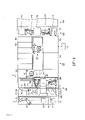
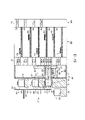
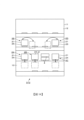
針對本發明之基板處理裝置之與第1實施型態有關的塗佈、顯像裝置1,分別參照圖1之橫斷俯視圖、圖2之縱斷側面圖而予以說明。塗佈、顯像裝置1係依照載體區塊D1、處理區塊D2、介面區塊D3之順序在橫向直線狀地被連接而構成。介面區塊D3連接有曝光機D4。The coating and developing
針對各區塊D1~D3簡單說明時,載體區塊D1被搬運收納有直徑為例如300mm之圓形基板亦即晶圓W的載體C,該載體區塊D1係將載體C內之晶圓W朝裝置內搬運。載體C係被稱為例如FOUP(Front Opening Unified Pod)之晶圓W之搬運容器,藉由容器本體,和被設置在該容器本體之前面的蓋部而構成。再者,上述處理區塊D2係對晶圓W供給各種藥液,進行反射防止膜之形成、光阻膜之形成,和根據顯像光阻膜的光阻圖案之形成。曝光機D4係曝光晶圓W以使在上述顯像形成光阻圖案,介面區塊D3係在處理區塊D2和曝光機D4之間收授晶圓W。When briefly describing each block D1-D3, the carrier block D1 is transported and accommodated with a circular substrate having a diameter of, for example, 300mm, that is, a carrier C that is a wafer W. Move it into the device. The carrier C is a transport container for a wafer W called, for example, a FOUP (Front Opening Unified Pod), and is constituted by a container body and a lid provided on the front surface of the container body. Moreover, the above-mentioned processing block D2 supplies various chemical solutions to the wafer W to form an anti-reflection film, a photoresist film, and a photoresist pattern according to the developed photoresist film. The exposure machine D4 is for exposing the wafer W to form a photoresist pattern during the above-mentioned development, and the interface block D3 is for receiving and delivering the wafer W between the processing block D2 and the exposure machine D4.
晶圓W係依照載體C→載體區塊D1→處理區塊D2→介面區塊D3→曝光機D4→介面區塊D3→處理區塊D2→載體區塊D1→載體C之順序被搬運而接受處理。在該搬運中,晶圓W係在朝處理區塊D2搬入前或從處理區塊D2搬出後,被搬運至被設置在載體區塊D1之檢查模組4,針對其表面之狀態被檢查。具體而言,針對例如有無異物或有無圖案大小之異常而進行檢查。之後,將在朝處理區塊D2搬入前進行的檢查記載為處理前檢查,將從處理區塊D2搬出後進行的檢查記載為處理後檢查。Wafer W is transported and received in the order of carrier C→carrier block D1→processing block D2→interface block D3→exposure machine D4→interface block D3→processing block D2→carrier block D1→carrier C deal with. In this transport, the wafer W is transported to the
接著,針對載體區塊D1也一面參照圖3之前視圖、圖4之斜視圖一面予以說明。另外,在圖4中,為了表示載體區塊D1之正面之各部,將載體區塊D1進行2分割成上下而予以表示。再者,在以下之說明中,將載體區塊D1側作為前方側,將介面區塊D3側作為後方側而予以說明,只要無特別說明,說明中的左側、右側就是從前方朝向後方觀看之時的左側、右側。Next, the carrier block D1 will also be described while referring to the front view of FIG. 3 and the perspective view of FIG. 4 . In addition, in FIG. 4, in order to show each part of the front surface of the carrier block D1, the carrier block D1 is shown divided into upper and lower parts. Furthermore, in the following descriptions, the side of the carrier block D1 is taken as the front side, and the side of the interface block D3 is taken as the rear side. Unless otherwise specified, the left and right sides in the description are viewed from the front to the rear. The left and right sides of the time.
載體區塊D1具備角型之框體11,框體11之各側壁被形成垂直。在上下方向彼此隔開的3處從側壁之一的正面壁12突出於前方側而形成3層棚架。將該3層之棚架中下層之棚架設為支持台13,將中層之棚架設為支持台14,將上層之棚架設為支持台15。再者,支持台13之下端部進一步朝前方突出,形成支持台16。該些支持台13~16係以可以在台上支持載體C之方式形成水平。The carrier block D1 has a corner-
在框體11之正面壁12中,在支持台13和支持台14之間,從左側朝向右側且以在一列彼此隔開之方式依序設置有晶圓W之搬運口21、晶圓W之搬運口21、檢查模組設置用之開口部22、晶圓W之搬運口21。上述開口部22為扁平的角型,在垂直方向彼此隔開地設置兩個。在支持台13,於各搬運口21之前方,設置有載置載體C之移動平台23。移動平台23係在對該移動平台23進行載體C之收授的前方位置,和經由搬運口21在載體C和框體11內之間用以收授晶圓W的後方位置之間進退。In the
在上述各搬運口21設置有升降門24。在該升降門24之前面,設置有無圖示之保持載體C之蓋部的保持機構,被構成能對在後方位置構成移動平台23上之載體C之容器本體,進行該蓋部之收授。再者,升降門24係在封閉搬運口21之封閉位置,和從該封閉位置後退及下降的開放搬運口21之開放位置之間移動。因此,升降門24進行搬運口21之開關和載體C之蓋部的開關。另外,上述開放位置在圖2、圖3中以一點鏈線表示。因此,將具備載置收納晶圓W之搬運容器的平台、對被載置於該平台之搬運容器搬入搬出晶圓W的搬運口,及進行該搬運口之開關及搬運容器之蓋部之開關的門部的機器,視為裝載埠時,在支持台13上設置有3個裝載埠。在各圖中,為了彼此區別該3個裝載埠,從左側朝向右側依序表示2A、2B、2C。
在正面壁12,於支持台14和支持台15之間,在上述裝載埠2C之搬運口21之垂直上方開口一個晶圓W之搬運口21。在支持台14中,如此被設置在支持台14、15間的搬運口21之前方,設置有先前已述之移動平台23,再者在該搬運口21設置有旋轉門25。圖5為旋轉門25之斜視圖,圖5中之26係被連接於旋轉門25之邊緣部的臂部。圖5中之27係連接臂部26之另一端的旋轉機構。在前後觀看時,旋轉機構27係使旋轉門25位於搬運口21之下方,同時繞著沿著前後方向之水平的旋轉軸R1旋轉。再者,圖5中之28係前後移動機構,使旋轉門25與旋轉機構27及臂部26一起朝前後移動。On the
旋轉門25係藉由前後移動機構28及旋轉機構27,在封閉搬運口21之封閉位置,和相對於該封閉位置後退並且旋轉90°之位置亦即開放搬運口21之開放位置之間移動。該開放位置係在圖2、圖3以一點鏈線表示,如圖3所示般,朝前後觀看在開放位置之旋轉門25相對於搬運口21於橫向偏移,並且位於開口部22之上方。再者,即使在旋轉門25之前面,與升降門24之前面相同,設置有保持載體C之蓋部的無圖示之保持機構,相對於被載置於支持台14之後方位置的移動平台23的容器本體,進行該蓋部的收授。即是,升降門25也進行搬運口21之開關和載體C之蓋部的開關。因此,旋轉門25、藉由該旋轉門25被開關的搬運口21及支持台14上之移動平台23也被構成為裝載埠,在圖中以2D表示。The revolving
再者,在支持台14中,於上述裝載埠2D之左側,於左右隔著間隔在一列設置有分別載置載體C之3個待機用平台29。朝前後方向觀看,該支持台14之待機用平台29分別被設置在開口部22之垂直上方、裝載埠2A之移動平台23之垂直上方、裝載埠2B之移動平台23之垂直上方。接著,當針對支持台15、16予以說明時,從左向右且以在一列隔著間隔之方式依序設置有在支持台15分別載置載體C的搬入用平台31、待機用平台29、待機用平台29、搬出用平台32。朝前後方向觀看,搬出用平台31及被設置在支持台15之各待機用平台29,位於上述支持台14之各待機用平台29之垂直上方,搬入用平台31位於支持台14之移動平台23之垂直上方。在支持台16,於例如較該支持台16之左右之中央更右側,在左右排成一列地設置有兩個待機用平台29。但是,即使在較左右之中央更左側設置有待機用平台29亦可。In addition, in the support table 14, on the left side of the above-mentioned
藉由後述載體搬運機構3,載體C在搬入用平台31和搬出用平台32和待機用平台29之間被搬運。搬入用平台31係無圖示之外部搬運機構為了將載體C搬入至載體區塊D1載置該載體C的平台。該外部搬運機構係接收被載置於搬出用平台32之載體C,從載體區塊D1搬出。再者,各待機用平台29係用以使將晶圓W搬入至裝置內之前的載體C及將晶圓W搬入至裝置內之後之空出的載體C待機的平台。因此,載體C係依照搬入用平台31→待機用平台29→裝載埠2A~2D中之任一的移動平台23之順序被搬運,在該移動平台23上,掃出晶圓W之後,依照待機用平台29→裝載埠2A~2D中之任一的移動平台23之順序被搬運而在該移動平台23上接收晶圓W。之後,載體C依照待機用平台29→搬出用平台32之順序被搬運。The carrier C is conveyed between the carry-in
然而,當針對待機用平台29予以補充時,因如上述般,在支持台14之右端部,設置裝載埠2D,故可以設置在支持台14之待機用平台29之數量不限。但是,除支持台14、15之外,因在裝載埠2A~2D之下方之支持台16也設置有待機用平台29,故可以將充分數量的載體C搬入至載體區塊D1。因此,可以確保高處理量。However, when supplementing the stand-
針對上述載體搬運機構3予以說明。載體搬運機構3被設置在載體區塊D1之正面壁12之前方側,具備可以保持被設置在載體C之上部的被保持部之多關節臂33,和使多關節臂33升降之升降機構34,和使升降機構34在左右移動的左右移動機構35,在上述路徑中搬運載體C。The above-mentioned
在載體區塊D1,設置有兩個用以進行晶圓W之檢查的檢查模組4。針對該檢查模組4,也一面參照圖6之縱斷側視圖,一面予以說明。檢查模組4具備有例如角型且前後長的扁平之框體41,框體41係經由上述開口部22從框體11之外部插入至框體11內,依此被設置在載體區塊D1。開口部22因被上下垂直配列,故檢查模組4也上下垂直配列。在框體41之後部之左右之側壁,分別形成有晶圓W之搬運口42,在框體112內開口。框體41之前方側從框體11之正面壁12突出。In the carrier block D1, two
在框體41內,吸附晶圓W之背面側中央部,設置有將晶圓W保持水平的載置部43。在框體41內,載置部43可以在後方側之待機位置和前方側之攝像完成位置之間移動。圖6中,以實線表示待機位置,以一點鏈線表示攝像完成位置。再者,在圖1中,表示在待機位置中的載置部43。待機位置係面臨上述搬運口42的位置,經由搬運口42而進入框體41內的後述搬運機構5A、5B之叉架56升降,依此在該搬運機構5A、5B和載置部43之間進行晶圓W之收授。另外,即使在框體41內設置升降自如的插銷,以取代叉架56升降,藉由該挿銷在搬運機構5A、5B和待機位置之載置部43之間進行晶圓W之收授亦可。圖中44係用以使載置部43在前後移動的移動機構。Inside the
在框體41內,根據載置部43的晶圓W之移動路之上方,設置有在框體41內左右延伸的橫長半鏡45,該半鏡45相對於晶圓W之移動方向被設置成側視傾斜。再者,在半鏡45之上方,設置隔著該半鏡45朝下方照射光之照明46。在半鏡45之深處設置有攝影機47。來自照明46之照射光通過半鏡45,被照射至半鏡45之下方的照射區域。而且,位於該照射區域中之物體的反射光,在半鏡45反射,並被攝影機47接收。即是,攝影機47可以攝像位於半鏡45之下方的攝像區域的物體。In the
在待機位置,從搬運機構5A或5B收授晶圓W的載置部43朝向攝像完成位置移動之期間,攝影機47進行間歇性攝像,依此攝像晶圓W之表面全體而取得畫像資料。該畫像資料從攝影機47被發送至後述控制部10,藉由控制部10,根據該畫像資料,進行晶圓W之表面的檢查。另外,移動至攝像完成位置的載置部43,為了將晶圓W收授至搬運機構5A或5B,返回至待機位置。In the standby position, while the
然而,檢查模組4被構成相對於載體區塊D1裝卸自如。例如,如圖7所示般,在載體區塊D1之開口部22之邊緣部,設置有朝向框體11內而沿著開口部22之開口方向延伸之導軌48以作為卡合部。另一方面,在檢查模組4之框體41,設置有從該框體41之後端朝向前方延伸之溝部49以作為被卡合部。如上述般,檢查模組4之框體41之後部被插入載體區塊D1之框體11內,檢查模組4被安裝於載體區塊D1之時,如圖7之上段所示般溝部49和導軌48卡合。However, the
例如,作業者將從開口部22突出之檢查模組4之前部朝前方牽引,依此框體41之後部沿著導軌48而拉出至框體11之外側,如圖7之下層所示般,溝部49從導軌48脫離,檢查模組4從載體區塊D1被拆下。於將檢查模組4安裝於框體41之時,進行與該拆卸之時相反的作業。如此一來,藉由檢查模組4相對於載體區塊D1裝卸自如,可以容易進行例如照明46之更換等之檢查模組4的維修。另外,在圖7以外之圖中省略導軌48及溝部49的表示。For example, the operator pulls the front part of the
接著,也一面參照圖8之載體區塊D1之縱斷前視圖,一面針對框體11內之構成予以說明。在框體11內,設置有緩衝模組51。該緩衝模組51係被構成在上下方向隔著間隔載置複數片晶圓W,例如,藉由在上下方向設置複數支撐晶圓W之背面之3根挿銷的組而被構成。另外,作為緩衝模組51,不限於具備如此之挿銷的構成,即使被構成例如以導引晶圓W之周緣部而使晶圓W落入至特定位置之方式,以碗狀支持該周緣部亦可。在該緩衝模組51被設置成在檢查模組4之上方,俯視觀看下重疊於該檢查模組4之載置部43之待機位置。該緩衝模組51構成至檢查模組4空出(即是,先前在檢查模組4進行檢查的晶圓W被搬出),能夠將後續之晶圓W搬入至該檢查模組4為止,載置該後續的晶圓W而使待機的待機部。Next, the configuration inside the
在緩衝模組51及檢查模組4之左側,設置有搬運機構5A,在右側設置有搬運機構5B。搬運機構5A藉由豎立之框架52、使框架52在左右移動之左右移動機構53、被設置成與框架52垂直升降自如的升降台54、在升降台54上繞垂直軸旋轉自如的基台55,和在基台55上進退自如並支撐晶圓W之背面的叉架56所構成。另外,上述框架52藉由左右移動機構53移動的區域,限於緩衝模組51及檢查模組4之左側。On the left side of the
第1基板搬運機構亦即搬運機構5A藉由構成該搬運機構5A之上述各部的合作作用,可以在被載置於第1裝載埠亦即裝載埠2A、2B的各載體C,和在檢查模組4之待機位置之載置部43,和緩衝模組51,和後述塔部T1之收授模組之間,收授晶圓W。另外,圖1中之57係為了如此地將晶圓W收授於塔部T1,被設置在框體11之後方側的晶圓W之搬運路。第2基板搬運機構亦即搬運機構5B除了不設置左右移動機構53之外,其他被構成與搬運機構5A相同。搬運機構5B藉由構成該搬運機構5B之各部之合作作用,可以在被載置於第2裝載埠亦即裝載埠2C、2D之各載體C,和在檢查模組4之待機位置之載置部43,和緩衝模組51之間收授晶圓W。如此一來,在緩衝模組51及檢查模組4之載置部43,搬運機構5A、5B之雙方可以收授晶圓W,該緩衝模組51及載置部43為了在該些搬運機構5A、5B間收授晶圓W,兼作載置該晶圓W之收授部使用。The
接著,使用圖1、圖2針對處理區塊D2予以說明。處理區塊D2係被構成從下方依序疊層對晶圓W進行液處理之第1~第6單位區塊E1~E6。E1和E2係彼此相同的單位區塊,E3和E4係彼此相同的單位區塊,E5和E6係彼此相同的單位區塊。兩個相同的單位區塊之中,晶圓W被搬運至一方之單位區塊。在此,單位區塊之中,以圖1所示之單位區塊E3為代表予以說明。以在前後延伸之方式,形成有晶圓W之搬運區域61,在搬運區域61之右側,於前後方向配置兩個光阻膜形成模組62,該光阻膜形成模組62係在晶圓W之表面塗佈光阻作為藥液而形成光阻膜。在搬運區域61之左側,沿著搬運區域61於前後設置有複數加熱晶圓W之加熱模組63。再者,在上述搬運區域61,設置有於單位區塊E3內搬運晶圓W之搬運機構F3。Next, the processing block D2 will be described using FIG. 1 and FIG. 2 . The processing block D2 is formed by sequentially stacking first to sixth unit blocks E1 to E6 for performing liquid processing on the wafer W from below. E1 and E2 are the same unit blocks as each other, E3 and E4 are the same unit blocks as each other, and E5 and E6 are the same unit blocks as each other. Among two identical unit blocks, the wafer W is transferred to one of the unit blocks. Here, among the unit blocks, the unit block E3 shown in FIG. 1 will be described as a representative. In the manner of extending forward and backward, a
當針對單位區塊E1、E2、E5、E6,說明與單位區塊E3、E4之差異點時,單位區塊E1、E2具備反射防止膜形成模組,取代光阻膜形成模組62。反射防止膜形成模組為了在晶圓W形成反射防止膜,塗佈反射防止膜形成用之藥液而形成反射防止膜,取代光阻。單位區塊E5、E6具備有顯像模組,取代光阻膜形成模組62。顯像模組對晶圓W供給顯像液作為藥液。針對如此地進行藥液之供給的模組,除了該藥液之種類不同之外,其他單位區塊E1~E6被構成彼此相同。再者,在圖2中,針對相當於搬運機構F3之各單位區塊E1、E2、E4~E6之搬運機構,表示為F1、F2、F4~F6。When describing the differences between the unit blocks E1 , E2 , E5 , and E6 from the unit blocks E3 , E4 , the unit blocks E1 , E2 are equipped with an antireflection film forming module instead of the photoresist
在處理區塊D2之載體區塊D1側,設置有跨越各單位區塊E1~E6而上下延伸,且由彼此被疊層之多數收授模組所構成之塔部T1,和用以在構成塔部T1之各模組間進行晶圓W之收授的搬運機構64。在塔部T1中,在設置例如單位區塊E1~E6的各高度,設置有載置晶圓W之收授模組TRS~TRS6。再者,在塔部T1如上述般為了在與搬運機構5A之間收授晶圓W,設置有載置晶圓W之收授模組,將該收授模組設為TRS0、TRS10。On the side of the carrier block D1 of the processing block D2, a tower part T1 extending up and down across the unit blocks E1-E6 and composed of stacked multi-receiver modules is provided, and is used for forming The
介面區塊D3具備橫跨單位區塊E1~E6而上下延伸之塔部T2、T3、T4,設置有用以對塔部T2和塔部T3進行晶圓W之收授的搬運機構65,和用以對塔部T2和塔部T4進行晶圓W之收授的搬運機構66,和用以在塔部T2和曝光裝置D4之間進行晶圓W之收授的搬運機構67。塔部T2疊層設置有用以對各單位區塊收授晶圓W之收授模組TRS。雖然在塔部T3、T4分別也設置有模組,但是針對該模組省略說明。The interface block D3 has towers T2, T3, and T4 extending up and down across the unit blocks E1 to E6, and is provided with a
如圖1所示般,在塗佈、顯像裝置1設置有由電腦所構成之控制部10。控制部10具有具備有程式之無圖示之程式儲存部。控制部10係對塗佈、顯像裝置1之各部輸出控制訊號,控制根據各搬運機構之晶圓W的搬運、根據載體搬運機構3之載體C的搬運,及在各模組中之晶圓的處理,如後述般,以對晶圓W進行光阻圖案之形成及檢查之方式,針對上述程式,編組命令。該程式係在被收納於例如硬碟、CD、光磁性碟或記憶卡等之記憶媒體之狀態下,被儲存於程式儲存部。As shown in FIG. 1 , a
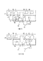
接著,一面參照圖9、圖10,一面說明進行上述光阻圖案之形成和處理前檢查之時的在載體區塊D1中之晶圓W的搬運路徑。在該圖9、圖10及後述圖11、圖12中,為了圖示方便,橫向排列表示裝載埠2C、2D,並且彼此錯開表示檢查模組4和緩衝模組51。Next, the transport path of the wafer W in the carrier block D1 when the formation of the photoresist pattern and the pre-processing inspection described above are performed will be described with reference to FIGS. 9 and 10 . In FIG. 9, FIG. 10 and the following FIG. 11 and FIG. 12, for the convenience of illustration, the
於進行處理前檢查之時,例如裝載埠2C、2D當作用以搬入晶圓W之搬入用裝載埠使用,裝載埠2A、2B當作用以從裝置內搬出晶圓W之搬出用裝載埠使用。首先,晶圓W從分別被載置於裝載埠2C、2D之載體C,藉由搬運機構5B被搬運至緩衝模組51(圖9中,箭號A1)。For pre-processing inspection, for example,
接著,當成為晶圓W能夠搬運至檢查模組4時,晶圓W藉由搬運機構5B被搬入至檢查模組4(圖9中,箭號A2),取得晶圓W之表面之畫像資料而進行檢查。然後,晶圓W藉由搬運機構5A從檢查模組4被搬出,被搬運至塔部T1之收授模組TRS0(圖9中,箭號A3)。被搬運至收授模組TRS0之晶圓W,如先前所述般被搬運至處理區塊D2、介面區塊D3、曝光機D4而形成光阻圖案之後,被搬運至塔部T1之收授模組TRS10。而且,藉由搬運機構5A,該晶圓W被搬運至裝載埠2A或2B之載體C(圖10中,箭號A4)。Next, when the wafer W can be transported to the
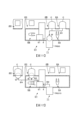
接著,一面參照圖11、圖12,一面說明進行上述光阻圖案之形成和處理後檢查之時的在載體區塊D1中之晶圓W的搬運路徑。於進行處理後檢查之情況,例如裝載埠2A、2B當作搬入用裝載埠使用,裝載埠2C、2D當作搬出用裝載埠使用。首先,晶圓W從分別被載置於裝載埠2A、2B之載體C,藉由搬運機構5A,被搬運至塔部T1之收授模組TRS0(圖11中,箭號B1)。該晶圓W如先前所述般,被搬運至處理區塊D2、介面區域D3、曝光機D4而形成光阻圖案之後,被搬運至塔部T1之收授模組TRS10。Next, the transport path of the wafer W in the carrier block D1 when the formation of the photoresist pattern and the post-processing inspection described above are performed will be described with reference to FIGS. 11 and 12 . In the case of post-processing inspection, for example, loading
接著,晶圓W藉由搬運機構5A,從收授模組TRS10被搬運至緩衝模組51(圖12中,箭號B2),當晶圓W能搬運至檢查模組4時,晶圓W藉由搬運機構5B被搬入至檢查模組4(圖12中,箭號B3),取得晶圓W之表面之畫像資料而進行檢查。而且,晶圓W藉由搬運機構5B從檢查模組4被搬出,被搬運至裝載埠2C或2D之載體C(圖12中,箭號B4)。Next, the wafer W is transported from the receiver module TRS10 to the
針對在上述晶圓W之各搬運中,從收授模組TRS0至收授模組TRS10的晶圓W之搬運路徑先予以說明。被搬運至收授模組TRS0之晶圓W藉由搬運機構64被分配搬運至單位區塊E1、E2。例如在將晶圓W收授至單位區塊E1之狀況,對塔部T1之收授模組TRS中,與單位區塊E1對應之收授模組TRS1(藉由搬運機構F1能夠收授晶圓W之收授模組)收授晶圓W。再者,在將晶圓W收授於單位區塊E2之情況,對塔部T1之收授模組TRS中,與單位區塊E2對應的收授模組TRS2,收授晶圓W。Among the above-mentioned transfers of the wafer W, the transfer route of the wafer W from the receiver module TRS0 to the receiver module TRS10 will be described first. The wafer W transported to the receiver module TRS0 is assigned and transported to the unit blocks E1 and E2 by the
如此被分配之晶圓W依照搬運機構F1(F2)依照TRS1(TRS2)→反射防止膜形成模組→加熱模組63→TRS1(TRS2)之順序被搬運,藉由搬運機構64被分配至與單位區塊E3對應的收授模組TRS3、和與單位區塊E4對應之收授模組TRS4。如此被分配至TRS3、TRS4之晶圓W藉由搬運機構F3(F4),依照TRS3(TRS4)→光阻膜形成模組62→加熱模組63→塔部T2之收授模組TRS31(TRS41)之順序被搬運。然後,該晶圓W藉由搬運機構65、67被搬運至曝光機D4,被形成在晶圓W之表面的光阻膜沿著特定圖案被曝光。The wafer W allocated in this way is transported in the order of TRS1 (TRS2)→anti-reflection film forming module→
曝光後之晶圓W藉由搬運機構66、67在塔部T2、T4間被搬運,分別被搬運至與單位區塊E5、E6對應之塔部T2的收授模組TRS51、TRS61。然後,晶圓W藉由搬運機構F5、F6依照加熱模組63→顯像模組之順序被搬運,光阻膜沿著在曝光機D4被曝光的圖案溶解而形成光阻圖案之後,被搬運至收授模組TRS10。The exposed wafer W is transported between the towers T2 and T4 by the
若藉由上述塗佈、顯像裝置1時,在被配置在載體區塊D1之左側的裝載埠2A、2B,和被配置在載體區塊D1之右側的裝載埠2C、2D之間設置有檢查模組4。而且,被配置在檢查模組4之左側的搬運機構5A對分別被載置於裝載埠2A、2B之載體C及處理區塊D2進行收授,被配置在檢查模組4之右側的搬運機構5B對分別被載置於裝載埠2C、2D之載體C進行收授,經由檢查模組4或緩衝模組51,在搬運機構5A、5B間收授晶圓W。若藉由如此之構成時,因可以將檢查模組4配置在裝載埠2A~2D之附近,故可以分別檢查剛被搬入至塗佈、顯像裝置1之後的晶圓W、從塗佈、顯像裝置1被搬出之前的晶圓W。因此,可以在朝塗佈、顯像裝置1搬入前晶圓W產生異常之情況,高精度地特定在顯像裝置1之外部產生的異常,且可以在塗佈、顯像裝置1內之處理及搬運產生異常之情況,確實地檢測出該異常。If the above-mentioned coating and developing
若能夠進行如此之檢查,而且藉由上述載體區塊D1之構成時,搬運機構5A、5B分別存取的裝載埠之數量被抑制,並且晶圓W對處理區塊D2之搬運,藉由搬運機構5A進行,另外,針對晶圓W朝檢查模組4之搬運,可以使用不對處理區塊D2進行搬運的搬運機構5B來進行。即是,因以搬運機構5A、5B分擔任務,故可以抑制為了在載體C和處理區塊D2之間,搬運晶圓W並且在搬運中進行檢查,搬運機構5A、5B分別進行晶圓W之收授的次數。即是,因抑制搬運機構5A、5B的各負載變大之情形,故可以提高裝置之處理量。If such an inspection can be performed, and with the above-mentioned configuration of the carrier block D1, the number of load ports accessed by the
而且,針對如上述般設置在左右之裝載埠間的檢查模組4,被設置成與裝載埠2A~2C之搬運口21相同高度。即是,被設置成檢查模組4和裝載埠2A~2C在左右構成列。依此,因可以使裝載埠2A~2C之載體C和檢查模組4之間之距離成為比較短,可以在該些裝載埠2A~2C和載體C之間快速搬運晶圓W,故可以更確實地提高裝置之處理量。另外,即使如上述般經由緩衝模組51在載體C和檢查模組4之間進行搬運之情況,若一列地配置檢查模組4和裝載埠2A~2C時,藉由在檢查模組4之附近配置緩衝模組51,因可以抑制搬運機構5A、5B之移動距離變長之情形,故可以進行快速的晶圓W之搬運。Furthermore, the
並且,雖然如上述般藉由邊設置裝載埠2A~2C,邊設置裝載埠2D,使不會引起因裝載埠之數量不足所致的處理量下降,但是藉由將該裝載埠2D,配置在裝載埠2C之上方,可以防止在上述位置設置檢查模組4並且設置4個裝載埠所致的載體區塊D1之佔地面積增大。並且,針對裝載埠2A~2C,藉由升降門24分別開關搬運口21,依此抑制為了開關搬運口21需要的左右空間,防止檢查模組4和裝載埠之間隔變大之情形,防止載體區塊D1之左右寬度增大。另一方面,針對裝載埠2D,藉由旋轉門25開關搬運口21,依此抑制為了開關搬運口21需要的上下空間,藉此被構成裝載埠2C、2D間之距離變短。即是,因即使在上下配置裝載埠2C、2D,搬運機構5B為了分別對各裝載埠2C、2D存取而升降的長度亦被抑制,故被構成可以更確實地提高處理量。Furthermore, although the
另外,雖然檢查模組4為了防止處理量下降設置兩個,但是即使設置僅設置一個亦可。再者,即使設置3個以上的檢查模組4亦可,即使在此情況,為了邊抑制裝置之佔地面積,邊使搬運機構5A、5B分別收授晶圓W,各檢查模組4設置成彼此疊層為佳。In addition, although two
另外,檢查模組4不限定於被設置成裝載埠2A~2C之搬運口21相同之高度,即使例如將緩衝模組51配置成與裝載埠2A~2C之搬運口21相同之高度,在較該緩衝模組51更高的位置設置檢查模組4亦可。但是,為了避免裝載埠2D之旋轉門25和檢查模組4之干擾,裝載埠2D相對於裝載埠2C之高度增加,使得上述搬運機構5B為了分別對裝載埠2C、2D存取而升降的長度有變大之虞,且也從上述般快速地進行裝載埠2A~2C之載體C和檢查模組4之間的搬運之觀點來看,以檢查模組4設置成與裝載埠2A~2C之搬運口21相同的高度為佳。In addition, the
再者,在俯視觀看下,因緩衝模組51被設置成與在檢查模組4之待機位置的載置部43重疊,故在搬運機構5A、5B設置叉架56之基台55不在左右移動,僅升降動作可以將在緩衝模組51待機之晶圓W搬運至檢查模組4。因此,緩衝模組51和檢查模組4之間的晶圓W之搬運所需的時間被抑制,可以更確實地提更處理量。另外,即使以在載體區塊D1不設置緩衝模組51,而在搬運機構5A、5B間的晶圓W之搬運僅經由檢查模組4進行之方式,例如將晶圓W搬入至檢查模組4之時,搬運機構5A、5B保持晶圓W並待機至檢查模組4空出亦可。但是,因如此在保持晶圓W之期間,搬運機構5A、5B無法進行其他晶圓W之搬運,故為了防止處理量之下降,以設置緩衝模組51為有效。Furthermore, in a plan view, since the
並且,在上述載體區塊D1中,檢查模組4之載置部43及緩衝模組51,為了在搬運機構5A、5B間進行晶圓W之收授,被構成載置晶圓W之收授部,但是即使檢查模組4及緩衝模組51個別地設置收授部亦可。但是,藉由檢查模組4兼作收授部使用,如圖9所示般,搬運機構5A直接接收檢查完的晶圓W,可以搬運至塔部T1。再者,藉由緩衝模組51兼作收授部使用,如圖12所示般,可以將塔部T1之晶圓W直接搬運至緩衝模組51並待機。即是,藉由檢查模組4及緩衝模組51分別兼作收授部使用,可以抑制搬運機構5A、5B之負載,可以謀求處理量之提升。In addition, in the above-mentioned carrier block D1, the
再者,不限於從載體C被搬出之晶圓W再次被收納於載體C為止,僅進行上述處理前檢查及處理後檢查中之一方。當表示處理前檢查及處理後檢查之搬運的一例時,首先,如以圖9之箭號A1~A3所示般,針對從裝載埠2C、2D被搬出之晶圓W,依照緩衝模組51、檢查模組4、收授模組TRS0之順序,對該晶圓W進行處理前檢查,朝處理區塊D2搬運。然後,將形成光阻圖案,且被搬運至收授模組TRS10之該晶圓W,如以圖12之箭號B2~B3所示般,依照緩衝模組51、檢查模組4之順序搬運,於進行處理後檢查之後,搬運至裝載埠2A、2B之載體C。如此一來,藉由進行處理前檢查及處理後檢查,在晶圓W檢測出異常之情況,可以更確實地特定該異常係起因於顯像裝置1,或起因於塗佈、顯像裝置1之外部。Note that only one of the above-mentioned pre-processing inspection and post-processing inspection is performed before the wafer W unloaded from the carrier C is stored in the carrier C again. When showing an example of transport of pre-processing inspection and post-processing inspection, first, as shown by arrows A1 to A3 in FIG. ,
針對進行處理前檢查之其他搬運例予以說明。如以圖9之箭號A1~A3所示般,將從裝載埠2C、2D之載體C搬出的晶圓W,依照緩衝模組51、檢查模組4、收授模組TRS0之順序搬運。然後,將形成光阻圖案而被搬運至收授模組TRS10之晶圓W,藉由搬運機構5A搬運至緩衝模組51,接著,藉由搬運機構5B,搬運至裝載埠2C、2D之載體C。即是,當將該一連串之搬運設為第1搬入搬出搬運時,在第1搬入搬出搬運中,裝載埠2C、2D構成搬入用裝載埠及搬出用裝載埠。Describes other handling examples where pre-processing inspections are performed. As shown by arrows A1-A3 in FIG. 9 , the wafer W carried out from the carrier C of the
針對進行處理後檢查之其他搬運例予以說明。如以圖11說明般,從裝載埠2A、2B之載體C被搬運至收授模組TRS0,然後,針對形成光阻圖案而被搬運至收授模組TRS10之晶圓W,如以圖12之箭號B2、B3所示般,依照緩衝模組51、檢查模組4之順序搬運。然後,將該晶圓W藉由搬運機構5A從檢查模組4搬運至裝載埠2A、2B之載體C。即是,當將該一連串之搬運設為第2搬入搬出搬運時,在第2搬入搬出搬運中,裝載埠2A、2B構成搬入用裝載埠及搬出用裝載埠。Explain other handling examples for post-processing inspection. As illustrated in FIG. 11 , the carrier C from the
例如,通常即使以如以圖9~圖12說明般進行晶圓W之搬運,當無法使用裝載埠2A、2B之雙方時,進行第1搬入搬出搬運,當無法使用裝載埠2C、2D之雙方時,進行第2搬入搬出搬運之方式,控制搬運亦可。再者,作為將例如兩個檢查模組4中之一方專門使用於第1搬入搬出搬運的模組,將另一方專門使用於第2搬入搬出搬運的模組,並行進行第1搬出搬入搬運和第2搬入搬出搬運亦可。即是,不限於如圖9~圖12所示之例般,以搬運機構5A、5B之中之一方僅進行接收來自載體C之晶圓W,搬運機構5A、5B之中之另一方僅進行朝載體C搬運晶圓W之方式,控制各搬運機構5A、5B之動作。For example, even if the wafer W is usually transported as described with reference to FIGS. 9 to 12 , when both of the
(第1實施型態之第1變形例)
接著,針對與第1實施型態之第1變形例有關之載體區塊D11,一面參照圖13,一面以與載體區塊D1之差異點為中心予以說明。在該載體區塊D11中,裝載埠2A被設置成與裝載埠2D相同高度,且與裝載埠2B左右之位置一致。作為開關該裝載埠2A之搬運口21的門部,以不干擾到裝載埠2B之方式,與裝載埠2D相同設置有旋轉門25。再者,在該裝載區塊D11中,在裝載埠2B之左側,與右側相同於上下設置有兩個檢查模組4。為了方便說明,將裝載埠2B之右側之兩個檢查模組設為4A,將左側之兩個檢查模組設為4B。針對檢查模組4B及裝載埠2A,位於檢查模組4A之左側,依此搬運機構5A進行晶圓W之收授。
(The first modified example of the first embodiment)
Next, the carrier block D11 related to the first modified example of the first embodiment will be described centering on differences from the carrier block D1 while referring to FIG. 13 . In the carrier block D11, the
當表示在載體區塊D11之搬運的一例時,例如,以如圖9所示般,從裝載埠2C、2D之載體C取出而被搬運至緩衝模組51之晶圓W,藉由搬運機構5B,被搬運至檢查模組4A,或藉由搬運機構5A被搬運至檢查模組4B而接受處理前檢查。檢查後之各晶圓W藉由搬運機構5A被搬運至塔部T1之收授模組TRS0。再者,作為其他搬運例,即使為了進行處理後檢查,將從收授模組TRS10被搬運至緩衝模組51之晶圓W,搬運至檢查模組4A、4B,然後,使返回至特定之裝載埠的載體C亦可。若藉由該載體區塊D11時,因比起第1實施型態,檢查模組4之數量多,故可以抑制晶圓W在緩衝模組51待機之時間。但是,因對比載體區塊D1更多之數量的檢查模組4存取,使得搬運機構5A、5B之負載變大,故為了取得更高的處理,以設為載體區塊D1之構成為更佳。When showing an example of transport in the carrier block D11, for example, as shown in FIG. 5B is transported to the
(第1實施型態之第2變形例)
接著,針對與第2變形例有關之載體區塊D12,一面參照圖14,一面以與載體區塊D1之差異點為中心予以說明。在該載體區塊D12中,除了裝載埠2A~2D之外,設置有裝載埠2E。該裝載埠2E被設置成與裝載埠2D相同高度,且與裝載埠2A左右之位置一致。裝載埠2E係以不干擾到裝載埠2A之方式,與裝載埠2D相同設置有旋轉門25。但是,以不干擾到載體區塊D1之框體11之側壁之方式,該裝載埠2E之旋轉門25與裝載埠2D之旋轉門25相反地從封閉位置順時鐘旋轉。因裝載埠2E位於檢查模組4之左側,故相對於被載置於該裝載埠2E之載體C,搬運機構5B收授晶圓W。
(The second modified example of the first embodiment)
Next, the carrier block D12 related to the second modified example will be described with reference to FIG. 14 focusing on differences from the carrier block D1. In this carrier block D12, in addition to the
在該載體區塊D12中,以例如圖9~圖12說明般地進行晶圓W之搬運,在裝載埠2A、2B成為搬入用裝載埠之時,例如裝載埠2E也成為搬入用裝載埠,在裝載埠2A、2B成為搬出用裝載埠之時,例如裝載埠2E也成為搬出用裝載埠。In the carrier block D12, the transfer of the wafer W is performed as described with reference to, for example, FIGS. 9 to 12 . When loading
如上述第1實施型態及各變形例所示般,若藉由本發明時,設置兩個搬運機構5A、5B,可以在藉由該些之中的任一搬運機構可進行晶圓W之搬運的區域,設置檢查模組4及裝載埠。因此,有針對該些檢查模組4及裝載埠2之配置的自由度高,容易因應需要的處理量或在檢查模組4檢查所需的時間等而進行裝置之設計的優點。As shown in the above-mentioned first embodiment and each modified example, if according to the present invention, two
[第2實施型態]
針對第2實施型態之塗佈、顯像裝置,以與第1實施型態之差異點為中心予以說明。圖15、圖16分別表示被設置在第2實施型態之塗佈、顯像裝置之載體區塊D5之前視圖、橫斷俯視圖。雖然在載體區塊D5,設置有裝載埠2A~2C及兩個檢查模組4,但是裝載埠2A~2C位於各檢查模組4之左側。再者,在載體區塊D5不設置支持台15、16、17,相對於載體區塊D5收授載體C的外部搬運機構,係將載體C收授至裝載埠2A~2C之移動平台23。然後,不進行在載體C之待機用平台29和搬入用平台31和搬出用平台32之間的搬運。再者,在框體11內,僅設置搬運機構5A、5B之中的搬運機構5A,以能相對於被載置於裝載埠2A~2C之各載體C,進行晶圓W之收授之方式,該搬運機構5A之框架52在左右方向移動。
[Second implementation type]
The coating and developing device of the second embodiment will be described focusing on the differences from the first embodiment. 15 and 16 respectively show a front view and a cross-sectional plan view of the carrier block D5 provided in the coating and developing device of the second embodiment. Although the carrier block D5 is provided with
搬運機構5A係從裝載埠2A~2C之載體C取出晶圓W而搬運至塔部T1之收授模組TRS0,將被搬運至塔部T1之收授模組TRS10之已形成完光阻圖案的晶圓W搬運至裝載埠2A~2C之載體C。在進行處理前處理之情況,晶圓W被搬運至收授模組TRS0之前,被搬運至檢查模組4而被檢查。在進行處理後檢查之情況,晶圓W於返回至載體C之前,被搬運至檢查模組4而被檢查。The
圖17係上述載體區塊D5之變形例,表示於前後觀看時在第1實施型態形成有裝載埠2D之搬運口21之區域,於上下隔著間隔設置有兩個檢查模組4之例。因此,在圖17所示之載體區塊D5中,4個檢查模組4被設置在上下方向。上述,因即使在說明的第2實施型態中,檢查模組4也與第1實施型態相同,被構成相對於載體區塊D5之框體11裝卸自如,故可以容易進行維修。FIG. 17 is a modified example of the above-mentioned carrier block D5, showing an example in which two
再者,針對檢查模組4,因如此地從框體41之外側被插入至該框體41之開口部22之構成,故該檢查模組4可以設置成其一部分從載體區塊之框體41突出。即是,因在裝置內之檢查模組4之佔有空間被抑制,故可以防止在裝置內設置或增設其他模組而使得無法設置該檢查模組4之情形。再者,如此一來,由於佔有空間小及相對於框體41裝卸自如,故有不會妨礙基板搬運機構之動作或其他模組之配置而容易增設檢查模組4之優點。另外,從第1實施型態、第2實施型態明顯可知,在將檢查模組4設為對框體41裝卸自如的構成的時候,針對在左右構成列的裝載埠和檢查模組4,檢查模組4即使位於列的端部亦可,即使位於列之中央部亦可。Furthermore, for the
然而,作為晶圓W從載體區塊D1被搬運,對該晶圓W進行處理的處理模組不限於上述例。例如,即使為在晶圓W塗佈絕緣膜形成用之藥液的模組亦可,對晶圓W供給洗淨液的洗淨模組亦可,即使為供給用以將晶圓W彼此貼合之接著劑的模組亦可。再者,即使設置例如經由能夠切換常壓氛圍和真空氛圍的裝載鎖定模組而形成真空氛圍的處理模組,在此情況,可以進行根據對晶圓W供給處理氣體的CVD、ALD或蝕刻等之處理。另外,本發明不限先前所述的各例,各例可以適當變更,或彼此組合。However, as the wafer W is conveyed from the carrier block D1, the processing module for processing the wafer W is not limited to the above example. For example, it may be a module for applying a chemical solution for forming an insulating film on the wafer W, a cleaning module for supplying a cleaning solution to the wafer W, or a module for supplying wafers W to each other. A module combined with an adhesive is also available. Furthermore, even if a processing module that forms a vacuum atmosphere via a load lock module capable of switching between a normal pressure atmosphere and a vacuum atmosphere is installed, in this case, CVD, ALD, etching, etc. by supplying a processing gas to the wafer W can be performed. processing. In addition, this invention is not limited to each example mentioned above, Each example can be changed suitably, or can be combined with each other.
C:載體
D1:載體區塊
D2:處理部
1:塗佈、顯像裝置
2A~2D:裝載埠
21:搬運口
23:移動平台
24:升降門
25:旋轉門
4:檢查模組
5A,5B:搬運機構
51:緩衝模組
C: Carrier
D1: carrier block
D2: Processing Department
1: Coating and developing
[圖1]為本發明之基板處理裝置之一實施型態的塗佈、顯像裝置之橫斷俯視圖。 [圖2]為上述塗佈、顯像裝置之縱斷側視圖。 [圖3]為構成上述塗佈、顯像裝置之載體區塊之前視圖。 [圖4]為上述載體區塊之斜視圖。 [圖5]為被設置在上述載體區塊之裝載埠之門部的概略斜視圖。 [圖6]為被設置在上述載體區塊之檢查模組之縱斷側視圖。 [圖7]為上述檢查模組之概略俯視圖。 [圖8]為上述載體區塊之縱斷前視圖。 [圖9]為表示在上述載體區塊之晶圓之搬運路徑的說明圖。 [圖10]為表示在上述載體區塊之晶圓之搬運路徑的說明圖。 [圖11]為表示在上述載體區塊之晶圓之搬運路徑的說明圖。 [圖12]為表示在上述載體區塊之晶圓之搬運路徑的說明圖。 [圖13]為表示載體區塊之其他構成的前視圖。 [圖14]為表示載體區塊之其他構成的前視圖。 [圖15]為表示載體區塊之其他構成的前視圖。 [圖16]為表示載體區塊之其他構成的縱斷側視圖。 [圖17]為表示載體區塊之其他構成的前視圖。 [FIG. 1] It is a cross-sectional top view of the coating and developing apparatus which is one embodiment of the substrate processing apparatus of this invention. [ Fig. 2 ] It is a vertical side view of the above-mentioned coating and developing device. [ Fig. 3 ] is a front view of a carrier block constituting the above-mentioned coating and developing device. [FIG. 4] It is a perspective view of the above-mentioned carrier block. [FIG. 5] It is a schematic perspective view of the door part of the loading port provided in the said carrier block. [FIG. 6] It is a longitudinal side view of the inspection module installed in the said carrier block. [Fig. 7] It is a schematic top view of the above-mentioned inspection module. [FIG. 8] It is a vertical front view of the said carrier block. [FIG. 9] It is an explanatory diagram showing the transport path of the wafer in the said carrier block. [FIG. [FIG. 10] It is an explanatory diagram showing the transport path of the wafer in the said carrier block. [FIG. [FIG. 11] It is an explanatory diagram showing the transport path of the wafer in the said carrier block. [FIG. [FIG. 12] It is an explanatory diagram showing the transport path of the wafer in the said carrier block. [FIG. [FIG. 13] It is a front view showing another structure of a carrier block. [FIG. 14] It is a front view showing another structure of a carrier block. [FIG. 15] It is a front view showing another structure of a carrier block. [FIG. 16] It is a vertical side view showing another structure of a carrier block. [FIG. 17] It is a front view showing another structure of a carrier block.
1:塗佈、顯像裝置
2A~2C:裝載埠
3:載體搬運機構
4:檢查模組
5A,5B:搬運機構
10:控制部
11:框體
12:載體區塊
16:支持台
21:搬運口
22:開口部
23:移動平台
24:升降門
29:待機用平台
33:多關節臂
34:升降機構
35:左右移動機構
41:框體
43:載置部
51:緩衝模組
57:搬運路
61:搬運區域
62:光阻膜形成模組
63:加熱模組
64:搬運機構
65:搬運機構
66:搬運機構
67:搬運機構
C:載體
D1:載體區塊
D2:處理部
D3:介面區塊
D4:曝光機
E3:單位區塊
T1~T4:塔部
F3:搬運機構
1: Coating and developing
Claims (5)
Applications Claiming Priority (2)
| Application Number | Priority Date | Filing Date | Title |
|---|---|---|---|
| JP2017118807A JP6863114B2 (en) | 2017-06-16 | 2017-06-16 | Substrate processing equipment, substrate processing method and storage medium |
| JP2017-118807 | 2017-06-16 |
Publications (2)
| Publication Number | Publication Date |
|---|---|
| TW202242553A TW202242553A (en) | 2022-11-01 |
| TWI790981B true TWI790981B (en) | 2023-01-21 |
Family
ID=64658413
Family Applications (2)
| Application Number | Title | Priority Date | Filing Date |
|---|---|---|---|
| TW107118879A TWI773764B (en) | 2017-06-16 | 2018-06-01 | Substrate processing apparatus, substrate processing method, and storage medium |
| TW111126817A TWI790981B (en) | 2017-06-16 | 2018-06-01 | Substrate processing equipment |
Family Applications Before (1)
| Application Number | Title | Priority Date | Filing Date |
|---|---|---|---|
| TW107118879A TWI773764B (en) | 2017-06-16 | 2018-06-01 | Substrate processing apparatus, substrate processing method, and storage medium |
Country Status (5)
| Country | Link |
|---|---|
| US (3) | US10615065B2 (en) |
| JP (2) | JP6863114B2 (en) |
| KR (2) | KR102451387B1 (en) |
| CN (2) | CN208589418U (en) |
| TW (2) | TWI773764B (en) |
Families Citing this family (4)
| Publication number | Priority date | Publication date | Assignee | Title |
|---|---|---|---|---|
| JP7437599B2 (en) | 2020-05-12 | 2024-02-26 | 東京エレクトロン株式会社 | Substrate processing equipment and substrate processing method |
| JP7419966B2 (en) | 2020-05-25 | 2024-01-23 | 東京エレクトロン株式会社 | Substrate processing equipment and substrate processing method |
| JP2022011348A (en) * | 2020-06-30 | 2022-01-17 | 東京エレクトロン株式会社 | Substrate processing device and substrate processing method |
| TWI764851B (en) * | 2021-02-05 | 2022-05-11 | 矽碁科技股份有限公司 | Miniaturized semiconductor manufacturing system |
Citations (7)
| Publication number | Priority date | Publication date | Assignee | Title |
|---|---|---|---|---|
| JPH07335709A (en) * | 1994-06-14 | 1995-12-22 | Hitachi Ltd | Vacuum treating device |
| JP2005101029A (en) * | 2003-09-22 | 2005-04-14 | Dainippon Screen Mfg Co Ltd | Substrate treating device and functional block combination system therefor |
| JP2005203440A (en) * | 2004-01-13 | 2005-07-28 | Tokyo Electron Ltd | Position adjusting method and substrate processing system |
| JP2006269672A (en) * | 2005-03-23 | 2006-10-05 | Tokyo Electron Ltd | Apparatus and method for coating/developing |
| JP2012019130A (en) * | 2010-07-09 | 2012-01-26 | Tokyo Electron Ltd | Coating and developing device, coating and developing method and storage medium |
| JP2013098476A (en) * | 2011-11-04 | 2013-05-20 | Tokyo Electron Ltd | Substrate processing system, substrate transfer method, program, and computer storage medium |
| TW201620065A (en) * | 2014-09-05 | 2016-06-01 | Rorze Corp | Loading port and loading port atmoshpere substitution method |
Family Cites Families (15)
| Publication number | Priority date | Publication date | Assignee | Title |
|---|---|---|---|---|
| JP3878441B2 (en) * | 2001-07-18 | 2007-02-07 | 大日本スクリーン製造株式会社 | Substrate processing equipment |
| JP3761081B2 (en) | 2001-11-09 | 2006-03-29 | 東京エレクトロン株式会社 | Substrate processing equipment |
| JP4252935B2 (en) * | 2004-06-22 | 2009-04-08 | 東京エレクトロン株式会社 | Substrate processing equipment |
| US8078311B2 (en) * | 2004-12-06 | 2011-12-13 | Tokyo Electron Limited | Substrate processing apparatus and substrate transfer method adopted in substrate processing apparatus |
| JPWO2007108315A1 (en) * | 2006-03-22 | 2009-08-06 | 株式会社荏原製作所 | Substrate processing apparatus and substrate processing method |
| JP2009231627A (en) * | 2008-03-24 | 2009-10-08 | Sokudo Co Ltd | Substrate treatment device |
| JP2011003819A (en) * | 2009-06-22 | 2011-01-06 | Tokyo Electron Ltd | Method of processing substrate, program, computer storage medium, and substrate processing system |
| JP5392190B2 (en) * | 2010-06-01 | 2014-01-22 | 東京エレクトロン株式会社 | Substrate processing system and substrate processing method |
| JP5482500B2 (en) * | 2010-06-21 | 2014-05-07 | 東京エレクトロン株式会社 | Substrate processing equipment |
| JP5408059B2 (en) * | 2010-07-09 | 2014-02-05 | 東京エレクトロン株式会社 | Coating, developing device, coating, developing method and storage medium |
| JP5713081B2 (en) * | 2010-07-09 | 2015-05-07 | 東京エレクトロン株式会社 | Coating and developing equipment |
| JP2012080077A (en) * | 2010-09-06 | 2012-04-19 | Tokyo Electron Ltd | Device and method for substrate processing |
| JP5978728B2 (en) * | 2012-04-12 | 2016-08-24 | 東京エレクトロン株式会社 | Substrate delivery apparatus, substrate delivery method and storage medium |
| JP6040883B2 (en) * | 2012-12-25 | 2016-12-07 | 東京エレクトロン株式会社 | Substrate transport apparatus, substrate transport method, and storage medium |
| JP6121832B2 (en) * | 2013-07-29 | 2017-04-26 | 株式会社Screenホールディングス | Substrate processing apparatus, substrate processing method, and substrate processing system |
-
2017
- 2017-06-16 JP JP2017118807A patent/JP6863114B2/en active Active
-
2018
- 2018-06-01 TW TW107118879A patent/TWI773764B/en active
- 2018-06-01 TW TW111126817A patent/TWI790981B/en active
- 2018-06-11 KR KR1020180066761A patent/KR102451387B1/en active IP Right Grant
- 2018-06-12 US US16/006,007 patent/US10615065B2/en active Active
- 2018-06-19 CN CN201820944150.1U patent/CN208589418U/en active Active
- 2018-06-19 CN CN201810632233.1A patent/CN109148329A/en active Pending
-
2020
- 2020-02-27 US US16/802,796 patent/US10916463B2/en active Active
- 2020-12-29 US US17/136,134 patent/US11545377B2/en active Active
-
2021
- 2021-03-24 JP JP2021050585A patent/JP7070748B2/en active Active
-
2022
- 2022-09-30 KR KR1020220124977A patent/KR102552935B1/en active IP Right Grant
Patent Citations (7)
| Publication number | Priority date | Publication date | Assignee | Title |
|---|---|---|---|---|
| JPH07335709A (en) * | 1994-06-14 | 1995-12-22 | Hitachi Ltd | Vacuum treating device |
| JP2005101029A (en) * | 2003-09-22 | 2005-04-14 | Dainippon Screen Mfg Co Ltd | Substrate treating device and functional block combination system therefor |
| JP2005203440A (en) * | 2004-01-13 | 2005-07-28 | Tokyo Electron Ltd | Position adjusting method and substrate processing system |
| JP2006269672A (en) * | 2005-03-23 | 2006-10-05 | Tokyo Electron Ltd | Apparatus and method for coating/developing |
| JP2012019130A (en) * | 2010-07-09 | 2012-01-26 | Tokyo Electron Ltd | Coating and developing device, coating and developing method and storage medium |
| JP2013098476A (en) * | 2011-11-04 | 2013-05-20 | Tokyo Electron Ltd | Substrate processing system, substrate transfer method, program, and computer storage medium |
| TW201620065A (en) * | 2014-09-05 | 2016-06-01 | Rorze Corp | Loading port and loading port atmoshpere substitution method |
Also Published As
| Publication number | Publication date |
|---|---|
| TW201921122A (en) | 2019-06-01 |
| TW202242553A (en) | 2022-11-01 |
| US20210118711A1 (en) | 2021-04-22 |
| US10615065B2 (en) | 2020-04-07 |
| KR20220137858A (en) | 2022-10-12 |
| CN208589418U (en) | 2019-03-08 |
| US10916463B2 (en) | 2021-02-09 |
| CN109148329A (en) | 2019-01-04 |
| TWI773764B (en) | 2022-08-11 |
| US11545377B2 (en) | 2023-01-03 |
| KR102451387B1 (en) | 2022-10-06 |
| JP2021106279A (en) | 2021-07-26 |
| US20180366356A1 (en) | 2018-12-20 |
| KR102552935B1 (en) | 2023-07-07 |
| KR20180137409A (en) | 2018-12-27 |
| JP7070748B2 (en) | 2022-05-18 |
| JP2019004072A (en) | 2019-01-10 |
| US20200203202A1 (en) | 2020-06-25 |
| JP6863114B2 (en) | 2021-04-21 |
Similar Documents
| Publication | Publication Date | Title |
|---|---|---|
| TWI790981B (en) | Substrate processing equipment | |
| JP5212165B2 (en) | Substrate processing equipment | |
| JP5880247B2 (en) | Substrate processing apparatus, substrate processing method, and storage medium | |
| JP5978728B2 (en) | Substrate delivery apparatus, substrate delivery method and storage medium | |
| JP2009081362A (en) | Substrate processing apparatus | |
| JP2013102235A (en) | Substrate processing apparatus | |
| KR101776964B1 (en) | Coating-developing apparatus | |
| TWI458038B (en) | Load port | |
| TW202236486A (en) | Substrate processing device and substrate processing method | |
| JP7251673B2 (en) | SUBSTRATE PROCESSING APPARATUS, SUBSTRATE PROCESSING METHOD, AND STORAGE MEDIUM | |
| JP3612265B2 (en) | Coating and developing equipment | |
| US20230106927A1 (en) | Substrate processing apparatus and substrate processing method | |
| JP7437599B2 (en) | Substrate processing equipment and substrate processing method | |
| CN214042007U (en) | Coating and developing device | |
| CN215576096U (en) | Substrate processing apparatus | |
| CN114551281A (en) | Substrate processing apparatus, substrate processing method, and storage medium | |
| JP2013069917A (en) | Substrate processing apparatus and substrate processing method and storage medium |