JP5978728B2 - Substrate delivery apparatus, substrate delivery method and storage medium - Google Patents
Substrate delivery apparatus, substrate delivery method and storage medium Download PDFInfo
- Publication number
- JP5978728B2 JP5978728B2 JP2012091111A JP2012091111A JP5978728B2 JP 5978728 B2 JP5978728 B2 JP 5978728B2 JP 2012091111 A JP2012091111 A JP 2012091111A JP 2012091111 A JP2012091111 A JP 2012091111A JP 5978728 B2 JP5978728 B2 JP 5978728B2
- Authority
- JP
- Japan
- Prior art keywords
- door
- opening
- wafer
- carrier
- substrate
- Prior art date
- Legal status (The legal status is an assumption and is not a legal conclusion. Google has not performed a legal analysis and makes no representation as to the accuracy of the status listed.)
- Active
Links
- 239000000758 substrate Substances 0.000 title claims description 37
- 238000002716 delivery method Methods 0.000 title claims 3
- 238000012546 transfer Methods 0.000 claims description 151
- 230000007246 mechanism Effects 0.000 claims description 79
- 238000005192 partition Methods 0.000 claims description 38
- 238000004590 computer program Methods 0.000 claims 2
- 235000012431 wafers Nutrition 0.000 description 170
- 238000012545 processing Methods 0.000 description 25
- 238000000576 coating method Methods 0.000 description 22
- 239000011248 coating agent Substances 0.000 description 21
- 238000000034 method Methods 0.000 description 20
- 230000007723 transport mechanism Effects 0.000 description 18
- 238000013507 mapping Methods 0.000 description 15
- 230000032258 transport Effects 0.000 description 15
- 238000010438 heat treatment Methods 0.000 description 10
- 238000004929 transmission Raman spectroscopy Methods 0.000 description 9
- 239000007788 liquid Substances 0.000 description 8
- 238000000072 solvent casting and particulate leaching Methods 0.000 description 6
- 101100476845 Arabidopsis thaliana SCPL1 gene Proteins 0.000 description 5
- 101150075071 TRS1 gene Proteins 0.000 description 5
- 238000011161 development Methods 0.000 description 5
- 230000003028 elevating effect Effects 0.000 description 4
- 238000003780 insertion Methods 0.000 description 4
- 230000037431 insertion Effects 0.000 description 4
- 210000000078 claw Anatomy 0.000 description 3
- 238000012790 confirmation Methods 0.000 description 3
- 238000001514 detection method Methods 0.000 description 3
- 230000003287 optical effect Effects 0.000 description 3
- 239000002245 particle Substances 0.000 description 3
- 230000002093 peripheral effect Effects 0.000 description 3
- 230000000630 rising effect Effects 0.000 description 3
- 101100309661 Arabidopsis thaliana SCPL3 gene Proteins 0.000 description 2
- 101100202553 Arabidopsis thaliana SCPL5 gene Proteins 0.000 description 2
- 230000001174 ascending effect Effects 0.000 description 2
- 238000000605 extraction Methods 0.000 description 2
- 230000001681 protective effect Effects 0.000 description 2
- 239000004065 semiconductor Substances 0.000 description 2
- 239000000126 substance Substances 0.000 description 2
- 101100476879 Arabidopsis thaliana SCPL2 gene Proteins 0.000 description 1
- 101100202547 Arabidopsis thaliana SCPL4 gene Proteins 0.000 description 1
- 101100202554 Arabidopsis thaliana SCPL6 gene Proteins 0.000 description 1
- 238000013459 approach Methods 0.000 description 1
- 230000005540 biological transmission Effects 0.000 description 1
- 230000000903 blocking effect Effects 0.000 description 1
- 101150117627 bpl1 gene Proteins 0.000 description 1
- 239000000969 carrier Substances 0.000 description 1
- 230000008602 contraction Effects 0.000 description 1
- 238000004519 manufacturing process Methods 0.000 description 1
- 238000007789 sealing Methods 0.000 description 1
- 238000000638 solvent extraction Methods 0.000 description 1
Images


Classifications
-
- H—ELECTRICITY
- H01—ELECTRIC ELEMENTS
- H01L—SEMICONDUCTOR DEVICES NOT COVERED BY CLASS H10
- H01L21/00—Processes or apparatus adapted for the manufacture or treatment of semiconductor or solid state devices or of parts thereof
- H01L21/67—Apparatus specially adapted for handling semiconductor or electric solid state devices during manufacture or treatment thereof; Apparatus specially adapted for handling wafers during manufacture or treatment of semiconductor or electric solid state devices or components ; Apparatus not specifically provided for elsewhere
- H01L21/67005—Apparatus not specifically provided for elsewhere
- H01L21/67242—Apparatus for monitoring, sorting or marking
- H01L21/67259—Position monitoring, e.g. misposition detection or presence detection
- H01L21/67265—Position monitoring, e.g. misposition detection or presence detection of substrates stored in a container, a magazine, a carrier, a boat or the like
-
- H—ELECTRICITY
- H01—ELECTRIC ELEMENTS
- H01L—SEMICONDUCTOR DEVICES NOT COVERED BY CLASS H10
- H01L21/00—Processes or apparatus adapted for the manufacture or treatment of semiconductor or solid state devices or of parts thereof
- H01L21/67—Apparatus specially adapted for handling semiconductor or electric solid state devices during manufacture or treatment thereof; Apparatus specially adapted for handling wafers during manufacture or treatment of semiconductor or electric solid state devices or components ; Apparatus not specifically provided for elsewhere
- H01L21/677—Apparatus specially adapted for handling semiconductor or electric solid state devices during manufacture or treatment thereof; Apparatus specially adapted for handling wafers during manufacture or treatment of semiconductor or electric solid state devices or components ; Apparatus not specifically provided for elsewhere for conveying, e.g. between different workstations
- H01L21/67763—Apparatus specially adapted for handling semiconductor or electric solid state devices during manufacture or treatment thereof; Apparatus specially adapted for handling wafers during manufacture or treatment of semiconductor or electric solid state devices or components ; Apparatus not specifically provided for elsewhere for conveying, e.g. between different workstations the wafers being stored in a carrier, involving loading and unloading
- H01L21/67772—Apparatus specially adapted for handling semiconductor or electric solid state devices during manufacture or treatment thereof; Apparatus specially adapted for handling wafers during manufacture or treatment of semiconductor or electric solid state devices or components ; Apparatus not specifically provided for elsewhere for conveying, e.g. between different workstations the wafers being stored in a carrier, involving loading and unloading involving removal of lid, door, cover
-
- H—ELECTRICITY
- H01—ELECTRIC ELEMENTS
- H01L—SEMICONDUCTOR DEVICES NOT COVERED BY CLASS H10
- H01L21/00—Processes or apparatus adapted for the manufacture or treatment of semiconductor or solid state devices or of parts thereof
- H01L21/67—Apparatus specially adapted for handling semiconductor or electric solid state devices during manufacture or treatment thereof; Apparatus specially adapted for handling wafers during manufacture or treatment of semiconductor or electric solid state devices or components ; Apparatus not specifically provided for elsewhere
- H01L21/677—Apparatus specially adapted for handling semiconductor or electric solid state devices during manufacture or treatment thereof; Apparatus specially adapted for handling wafers during manufacture or treatment of semiconductor or electric solid state devices or components ; Apparatus not specifically provided for elsewhere for conveying, e.g. between different workstations
- H01L21/67763—Apparatus specially adapted for handling semiconductor or electric solid state devices during manufacture or treatment thereof; Apparatus specially adapted for handling wafers during manufacture or treatment of semiconductor or electric solid state devices or components ; Apparatus not specifically provided for elsewhere for conveying, e.g. between different workstations the wafers being stored in a carrier, involving loading and unloading
- H01L21/67775—Docking arrangements
-
- H—ELECTRICITY
- H01—ELECTRIC ELEMENTS
- H01L—SEMICONDUCTOR DEVICES NOT COVERED BY CLASS H10
- H01L21/00—Processes or apparatus adapted for the manufacture or treatment of semiconductor or solid state devices or of parts thereof
- H01L21/67—Apparatus specially adapted for handling semiconductor or electric solid state devices during manufacture or treatment thereof; Apparatus specially adapted for handling wafers during manufacture or treatment of semiconductor or electric solid state devices or components ; Apparatus not specifically provided for elsewhere
- H01L21/677—Apparatus specially adapted for handling semiconductor or electric solid state devices during manufacture or treatment thereof; Apparatus specially adapted for handling wafers during manufacture or treatment of semiconductor or electric solid state devices or components ; Apparatus not specifically provided for elsewhere for conveying, e.g. between different workstations
- H01L21/67763—Apparatus specially adapted for handling semiconductor or electric solid state devices during manufacture or treatment thereof; Apparatus specially adapted for handling wafers during manufacture or treatment of semiconductor or electric solid state devices or components ; Apparatus not specifically provided for elsewhere for conveying, e.g. between different workstations the wafers being stored in a carrier, involving loading and unloading
- H01L21/67778—Apparatus specially adapted for handling semiconductor or electric solid state devices during manufacture or treatment thereof; Apparatus specially adapted for handling wafers during manufacture or treatment of semiconductor or electric solid state devices or components ; Apparatus not specifically provided for elsewhere for conveying, e.g. between different workstations the wafers being stored in a carrier, involving loading and unloading involving loading and unloading of wafers
Landscapes
- Engineering & Computer Science (AREA)
- Physics & Mathematics (AREA)
- Condensed Matter Physics & Semiconductors (AREA)
- General Physics & Mathematics (AREA)
- Manufacturing & Machinery (AREA)
- Computer Hardware Design (AREA)
- Microelectronics & Electronic Packaging (AREA)
- Power Engineering (AREA)
- Container, Conveyance, Adherence, Positioning, Of Wafer (AREA)
Description
本発明は、隔壁の一方側の基板搬送領域と隔壁の他方側を搬送される搬送容器との間で基板を受け渡す基板受け渡し装置、基板受け渡し方法及び前記基板受け渡し方法を実行させるためのプログラムを記憶した記憶媒体に関する。 The present invention provides a substrate transfer apparatus, a substrate transfer method, and a program for executing the substrate transfer method for transferring a substrate between a substrate transfer region on one side of the partition and a transfer container transferred on the other side of the partition. The present invention relates to a stored storage medium.
半導体デバイスの製造プロセスにおいては、例えば半導体ウエハ(以下ウエハと記載する)に対してレジスト塗布処理や前記現像処理を行う塗布、現像装置が用いられる。この塗布、現像装置は外部から搬送されたキャリアが受け渡されるキャリアブロックを備え、当該キャリアブロックにはキャリアに格納されたウエハを装置内に搬送するロードポートが設けられている。外部から装置内へのパーティクルの進入を防ぐため、装置内部のウエハの搬送領域と装置外部のキャリアの搬送領域とは、前記ロードポートの隔壁により区画される。この隔壁にはウエハの搬送口が形成され、この搬送口はFIMS(Front-opening Interface Mechanical Standard)規格に従ったドアにより開閉される。特許文献1にはこのようなロードポートについて示されている。 In the manufacturing process of a semiconductor device, for example, a coating and developing apparatus that performs resist coating processing and development processing on a semiconductor wafer (hereinafter referred to as a wafer) is used. The coating / developing apparatus includes a carrier block to which a carrier conveyed from the outside is transferred, and the carrier block is provided with a load port for conveying a wafer stored in the carrier into the apparatus. In order to prevent particles from entering the apparatus from the outside, a wafer transfer area inside the apparatus and a carrier transfer area outside the apparatus are partitioned by the partition of the load port. A wafer transfer port is formed in the partition wall, and the transfer port is opened and closed by a door according to FIMS (Front-opening Interface Mechanical Standard) standard. Patent Document 1 discloses such a load port.
図31、32は、前記ロードポートの一例を示す縦断側面図であり、夫々ウエハ搬送口22が閉じられた状態、開かれた状態を示している。これらの図に示すように、ドア91はウエハ搬送口22を開閉するために昇降するのでロードポートの高さが比較的大きくなる。従って、塗布、現像装置にウエハWを速やかに大量に搬入することを目的としてロードポートを複数設ける場合、装置が設置されるクリーンルームの天井に前記キャリアブロックが抵触しないようにするために、ロードポートは横方向に配列されることになる。その結果、キャリアブロックひいては塗布、現像装置のフットプリント(占有床面積)が大きくなってしまうおそれがある。
31 and 32 are longitudinal side views showing an example of the load port, and show a state where the
また図中92はドア91の昇降用の駆動機構である。93は仕切り部材であり、駆動機構92をウエハ搬送領域17から区画する。94は接続部材であり、ドア91と駆動機構92とを接続する。前記仕切り部材93には、前記接続部材94が移動するために、縦に比較的長く伸びるスリット95が設けられる。このようにスリット95の長さが大きいため、駆動機構92から発生するパーティクルのウエハ搬送領域17へ流出を防ぐことが難しかった。
In the figure,
また、図中6はキャリアCのウエハWの配置状態を確認するためのマッピングユニットであり、特許文献2にその一例が記載されている。マッピングユニット6については実施の形態で詳細に説明するのでここでは簡単に説明するが、キャリアCからウエハWを搬出する前にキャリアC内のウエハWの配置状態を検出するためのセンサ部65を備える。このセンサ部65は、昇降自在且つその基端側が水平軸回りに回動自在な支持アーム64の先端に設けられ、前記回動動作によりウエハ搬送領域17とキャリアC内との間で進退する。
ドア91が上記のようにウエハ搬送口22から下降するため、支持アーム64は当該ドア91に干渉しないように、図31に示すように起立した状態でウエハ搬送口22の上方側で待機する。そして、ウエハ搬送口22の解放後、支持アーム64の下降動作、センサ部65のキャリアC内の下方側への進入動作、センサ部65のキャリアC内における上昇動作が順次行われ、この上昇動作中にセンサ部65によってウエハWの光学的な検出が行われる。図32は、この上昇動作を終えた状態のセンサ部65を示している。
Since the
しかしこのように光学的な検出を行った後、当該支持アーム64を図31の待機位置に戻すためには、隔壁18及びキャリアCに対する干渉を防ぐために当該支持アーム64を図32に示したキャリアC内の上昇位置から一旦下降させ、その後に回動動作を行い起立させて、再度上昇させる必要がある。このようにドア3がウエハ搬送口22に対して下降する構成にすると、マッピングユニット6の配置が制限され、それによって当該ユニット6の動作が制限される結果、前記配置状態の確認に要する時間を短縮することが難しかった。特許文献1、2には、これらのようなドアが昇降することにより起こる各種の問題について着目されておらず、当該問題を解決できるものではない。
However, in order to return the
本発明は上記の点に鑑みてなされたものであり、その目的は、基板受け渡し装置の高さを小さくすることができる技術を提供することである。 The present invention has been made in view of the above points, and an object of the present invention is to provide a technique capable of reducing the height of the substrate transfer device.
本発明の基板受け渡し装置は、隔壁に形成された開口部に、基板搬送容器の前面に形成された基板取り出し口を当該隔壁の一面側から対向させ、前記基板搬送容器の蓋体を前記隔壁の他面側から取り外して、基板の受け渡しを行う装置において、
前記開口部を前記隔壁の他面側から開閉するドアと、
前記ドアを、前記開口部を塞ぐ第1の位置と当該位置に対して前記隔壁の一面側から前記開口部に向かって見て前方に離れた第2の位置との間で進退させるための進退部と、
前記ドアを、第2の位置と前記開口部の前方領域から外れた第3の位置との間で、当該ドアの進退方向に沿った回動軸の周りに回動させる回動機構と、
を備え、
前記回動機構は、ロッドを直動移動させるシリンダと、前記ロッドと前記ドアとを接続し、当該ロッドの直動移動に連動して前記ドアを回転させるためのリンク部材と、により構成され、
前記進退部は、前記ドアと共に前記回動機構を進退させることを特徴とする。
In the substrate transfer apparatus of the present invention, a substrate take-out port formed on the front surface of the substrate transport container is opposed to an opening formed in the partition wall from one side of the partition wall, and the lid of the substrate transport container is attached to the partition wall. In the device that removes from the other side and delivers the substrate,
A door that opens and closes the opening from the other surface side of the partition;
Advancement / retraction for advancing / retreating the door between a first position that closes the opening and a second position that is separated from the position toward the opening from one side of the partition wall. And
A rotation mechanism for rotating the door about a rotation axis along the advancing / retreating direction of the door between a second position and a third position deviating from the front region of the opening ;
With
The rotating mechanism is composed of a cylinder that linearly moves a rod, and a link member that connects the rod and the door and rotates the door in conjunction with the linear movement of the rod,
The advance / retreat unit is configured to advance and retract the rotation mechanism together with the door.
本発明の具体的な態様としては下記の通りである。
(a)前記回動機構は、一端側が前記回動軸に固定され、他端側が前記ドアの中心部から左右方向及び上下方向に偏心した位置に固定された回動部材を備える。
(b)前記開口部、ドア、進退部及び回動機構の組が互いに上下に複数設けられる。
(c)前記開口部、ドア、進退部及び回動機構の組が互いに左右に複数設けられる。
(d)前記第3の位置は、第2の位置の左右方向に離れた位置に設定されている。
(e)前記第3の位置は、第2の位置の上下方向に離れた位置に設定されている。
(f)互いに隣接する、前記開口部、ドア、進退部及び回動機構の組のうちの一方の組の第3の位置と、他方の組の第3の位置とは、互いに前後に重なっている。
Specific embodiments of the present invention are as follows.
(A) the rotation mechanism, one end of which is fixed to the rotating shaft, the other end provided with a left-right direction and the rotating member fixed to a position eccentric in the vertical direction from the center portion of the door.
(B) A plurality of sets of the opening, the door, the advance / retreat part, and the rotation mechanism are provided above and below each other.
(C) A plurality of sets of the opening, the door, the advance / retreat part, and the rotation mechanism are provided on the left and right.
(D) The third position is set to a position away from the second position in the left-right direction.
( E ) The third position is set at a position away from the second position in the vertical direction.
( F ) The third position of one set of the set of the opening, door, advance / retreat section, and rotation mechanism adjacent to each other and the third position of the other set overlap each other in the front-rear direction. Yes.
本発明によれば、隔壁に形成された開口部に設けられるドアを、前記開口部を塞ぐ第1の位置と当該位置から前方に離れた第2の位置との間で進退させるための進退部と、前記ドアを、第2の位置と前記開口部の前方領域から外れた第3の位置との間で、当該ドアの進退方向に沿った回動軸の周りに回動させる回動機構と、が設けられる。このように構成することによってドアを昇降させる必要が無くなるので、当該ドアを開閉するために要する装置の高さを抑えることができる。 According to the present invention, the advancing / retreating portion for advancing / retreating the door provided in the opening formed in the partition wall between the first position blocking the opening and the second position away from the position forward. And a rotation mechanism for rotating the door about a rotation axis along the advancing / retreating direction of the door between a second position and a third position deviated from the front area of the opening. Are provided. With this configuration, it is not necessary to raise and lower the door, so that the height of the device required to open and close the door can be suppressed.
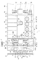
本発明の基板受け渡し装置が適用された塗布、現像装置1について説明する。図1、図2、図3は、夫々前記塗布、現像装置1の平面図、同概略斜視図、同概略側面図である。塗布、現像装置1は、キャリアブロックA1と、処理ブロックA2と、インターフェイスブロックA3と、を直線状に接続して構成されている。インターフェイスブロックA3には、処理ブロックA2の反対側に露光装置A4が接続されている。塗布、現像装置1の外側は、ウエハWを収納した基板搬送容器であるキャリアCの搬送領域11として構成されている。
The coating and developing apparatus 1 to which the substrate transfer apparatus of the present invention is applied will be described. 1, 2 and 3 are a plan view, a schematic perspective view and a schematic side view of the coating and developing apparatus 1, respectively. The coating / developing apparatus 1 is configured by linearly connecting a carrier block A1, a processing block A2, and an interface block A3. An exposure apparatus A4 is connected to the interface block A3 on the opposite side of the processing block A2. The outside of the coating / developing apparatus 1 is configured as a
各ブロックの役割を簡単に説明しておくと、キャリアブロックA1は本発明の基板受け渡し装置に相当し、図2に示す天井搬送機構12との間でウエハWを格納したキャリアCの受け渡しを行う。そして、受け渡されたキャリアCからウエハWを塗布、現像装置1に搬入し、塗布、現像装置1で処理されたウエハWをキャリアCに戻す。なお、前記天井搬送機構12は、クリーンルーム内の天井を介してキャリアCを、当該クリーンルームに設置された各装置間で受け渡す装置である。処理ブロックA2は、ウエハWにレジスト塗布処理、現像処理などの各種液処理や加熱処理を行うためのブロックである。露光装置A4は、処理ブロックA2にてウエハWに形成されたレジスト膜を露光する。インターフェイスブロックA3は、処理ブロックA2と露光装置A4との間でウエハWの受け渡しを行う役割を有する。
The role of each block will be briefly described. The carrier block A1 corresponds to the substrate transfer apparatus of the present invention, and transfers the carrier C storing the wafer W to and from the
キャリアブロックA1の構成について説明する。説明の便宜上、キャリアブロックA1側を前側、露光装置A4側を後側とする。キャリアブロックA1は、筐体13を備え、筐体13の内部はキャリア搬送領域11から区画されている。筐体13は角型のブロックの前面が前方に向かって上下3段に突出して棚状に形成されており、下段の棚、中段の棚、上段の棚は夫々キャリア載置棚14、15、16を構成している。筐体13内において、キャリア載置棚14〜16の後方側の空間はウエハWの搬送領域17として構成されている。
The configuration of the carrier block A1 will be described. For convenience of explanation, the carrier block A1 side is the front side, and the exposure apparatus A4 side is the rear side. The carrier block A <b> 1 includes a housing 13, and the inside of the housing 13 is partitioned from the
キャリアブロックA1の正面を示した図4も参照しながら説明する。筐体13の前面は、キャリアCからウエハWの搬入を行うロードポート2として構成されている。このロードポート2は、キャリアCを載置するステージ21と、ウエハWの搬送口22と、このウエハ搬送口22を開閉するドア3と、マッピングユニット6とにより構成される。このキャリアブロックA1には4つのロードポート2が設けられており、便宜上各ロードポート2を区別するために2A〜2Dの符号を付して示している。ロードポート2はキャリアブロックA1を正面から見て、上下左右に互いに離れて設けられており、右下側のロードポートを2A、左下側のロードポートを2B、右上側のロードポートを2C、左上側のロードポートを2Dとしている。ロードポート2A、2Bが互いに同じ高さに設けられ、ロードポート2C、2Dが互いに同じ高さに設けられている。ロードポート2A、2Cは互いに左右の同じ位置に設けられ、ロードポート2B、2Dは左右の同じ位置に設けられている。
The description will be made with reference to FIG. 4 showing the front of the carrier block A1. The front surface of the housing 13 is configured as a
各ロードポート2のウエハ搬送口22は、筐体13を構成する前方側の隔壁18に前後方向に開口しており、ロードポート2A、2Bのウエハ搬送口22は、キャリア載置棚14、15間に、ロードポート2C、2Dのウエハ搬送口22は、キャリア載置棚15、16間に夫々設けられている。各ウエハ搬送口22は平面視、概ね横長の四角形状に形成されている。前記隔壁18の前面側において、各ウエハ搬送口22の周囲には環状の凹部19が形成されており、ウエハWの受け渡し時にはキャリアCの前面が当該凹部19の前面に近接する。
The
キャリア載置棚14、15において各ウエハ搬送口22の手前側に前記ステージ21が設けられている。これらステージ21は、後退位置と前進位置との間で移動自在に構成されており、前記後退位置(アンローディング位置)は後述のキャリア搬送機構33との間でキャリアCを受け渡すための位置であり、前記前進位置(ローディング位置)は、キャリアCがウエハWを受け渡すために前記凹部19に近接する位置である。図中23はステージ21に設けられるピンであり、キャリアCの下方に形成される凹部に差し込まれ、ステージ21上にてキャリアCの位置ずれを防ぐ。
In the
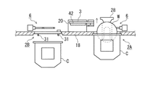
各ロードポート2は略同様に構成されており、これ以降代表してロードポート2Aについて説明する。図5、図6、図7は、夫々ロードポート2Aのドア3の正面図、縦断側面図、斜視図である。ドア3は前記ウエハ搬送口22を塞ぐことができるように概ね四角形状に形成されている。ドア3の正面には、その左右にキャリアCの蓋体42の着脱を行うための着脱機構を構成するキー31が設けられている。キー31はドア3から正面側に向かうように形成され、その先端が上下方向に伸びている。キー31は、前後方向の軸周りに回動する。
Each
ここでキャリアCの構成について、図7を参照しながら説明する。キャリアCは概ね角型の容器本体41と、角板状の蓋体42とからなる。容器本体41の上部には、上記の天井搬送機構12及び後述のキャリア搬送機構33がキャリアCを搬送するために把持するための被把持部43が設けられている。容器本体41の内部の左右には、内側に向かって突出部が多段に設けられ、この突出部間のスロット44にウエハWの周縁部が差し込まれて、ウエハWが多段に水平に保持される。容器本体41の前面にはウエハWの取り出し口45が形成され、前記蓋体42はこの取り出し口45を塞ぐように形成される。
Here, the configuration of the carrier C will be described with reference to FIG. The carrier C includes a substantially
蓋体42の前面には前記キー31が差し込まれる差し込み口46が形成され、キー31がこの差し込み口46に差し込まれた状態で回動すると、蓋体42内部の回動機構47が回動することにより、蓋体42の上下の側部にて爪部48が突没する。前記上下の側部から突出した爪部48が取り出し口44の上下の内縁部に形成される溝部49に差し込まれることによって、蓋体42と容器本体41とが係合する。爪部48が蓋体42の側部に没して溝部49から外れると、蓋体42と容器本体41との係合が解除され、差し込み口46に差し込まれたキー31に蓋体42が保持される。
An
ロードポート2Aの説明に戻る。ロードポート2Aは、キャリア載置棚14内の空間にドア開閉用駆動機構5を備えている。このドア開閉用駆動機構5は、ウエハ搬送口22に対してドア3を進退させるための進退機構51と、当該進退機構51に設けられ、ドア3が後退したときに当該ドア3を回動させるための回動機構52とにより構成される。前記進退機構51は、ガイドレール53と、スライダ54と、シリンダ55とにより構成される。ガイドレール53は前後方向に伸び、スライダ54がこのガイドレール53に係止されている。シリンダ55は前後方向に伸縮駆動し、それによって当該シリンダ55に接続されたスライダ54がガイドレール53に沿って進退するように構成されている。
Returning to the description of the
前記回動機構52は前記スライダ54に設けられており、シリンダ56と、リンク部材57と、回動部材をなすドア接続部58とにより構成されている。スライダ54上に前記シリンダ56が設けられ、シリンダ56は横方向に伸縮駆動する。リンク部材57は、シリンダ56とドア接続部58の一端側とに接続されており、シリンダ56に接続される軸59と、前記ドア接続部58に接続される軸50とを備え、各軸59、50は前後方向に向かって形成されている。ドア接続部58は図6に示すように側面視L字状に形成されており、その他端は後方側に向かった後、屈曲されて上方へと向かい、ドア3の裏面下端部に固定されている。このドア3におけるドア接続部58の固定位置は左右方向に見ると、キャリアブロックA1の中央部寄りである。つまり、この固定位置は、ドア3の中心部から左右方向及び上下方向に偏心した位置である。
The
シリンダ56の伸縮動作により、リンク部材57は軸59を回動軸として回動し、その傾きが変化する。そして前記リンク部材57の傾きの変化が、ドア3の軸50を回動軸とした回動動作に変換される。図8、9は、上記の回動によりドア3が開かれる様子を示しており、これらの図に示すようにドア3はその側部が下方向に向かい、キャリアブロックA1の内側へと倒れるように回動して、ウエハ搬送口22が開かれる。図10はウエハ搬送口22を開いたときのドア3を示す斜視図である。この図10及び他の各図中に示す20は、ウエハ搬送口22を開いたドア3を支持する支持部材である。
By the expansion / contraction operation of the
続いてマッピングユニット6について説明する。マッピングユニット6はウエハ搬送領域17に設けられており、ウエハ搬送口22を開いた後、キャリアCからウエハ搬送領域17にウエハWを搬入する前に、キャリアC内におけるウエハWの配置状態を確認するためのユニットである。配置状態の確認とは、具体的にはキャリアCの各スロット44におけるウエハWの有無の確認及び格納されているウエハWが水平か傾いているかの確認である。マッピングユニット6は、昇降機構61と、回動機構62と、支持シャフト63と、支持アーム64、64と、センサ部65とを備えている。
Next, the
前記昇降機構61は、ウエハ搬送口22の外側を上下に伸びるように設けられている。回動機構62は、前記昇降機構61により昇降自在に構成されており、昇降機構61より搬送口22側に設けられている。支持シャフト63は回動機構62から搬送口22側に向かって水平方向に伸びており、回動機構62により軸回りに回動する。支持シャフト63から2本の支持アーム64が支持シャフト63の軸方向と直交するように延び出している。支持アーム64、64は間隔をおき、互いに並行するように設けられている。支持アーム64、64の先端に前記センサ部65が設けられている。センサ部65は、互いに対になる発光部66及び受光部67により構成されており、一つの支持アーム64にこれら発光部66、受光部67のうち一方が設けられている。
The elevating
図11はキャリアCの横断平面図である。キャリアCにおける前記ウエハの配置状態を確認するときには支持アーム64、64が水平になり、この図11に示すように発光部66及び受光部67はキャリアC内に進入する。発光部66と受光部67との間には図11中点線の矢印で示す光軸が、キャリアCに格納されたウエハWに平面視重なるように形成される。
FIG. 11 is a cross-sectional plan view of the carrier C. When confirming the arrangement state of the wafer on the carrier C, the
受光部67は発光部66からの光の受光の有無に従って、後述の制御部7に検出信号を送信する。そして、前記光軸が形成された状態でセンサ部65が上昇し、制御部7は前記検出信号に基づいて、各スロット44におけるウエハWの有無を検出することができる。また、ウエハWの一端側と他端側が高さの異なるスロット44に進入し、ウエハWが傾いて保持されている場合は、水平に保持されている場合に比べて、ウエハWの見かけの厚さが大きくなるため、制御部7はこのようなウエハWの傾きの有無についても検出することができる。ウエハWの配置状態の検出を行う場合の他は、ウエハWの搬送を妨げないように、支持アーム64及びセンサ部65は、図5に示すウエハ搬送口22の下方の外側の待機位置にて待機する。
The
ロードポート2B〜2Dについて説明する。ロードポート2Bのドア3は、キャリアブロックA1の内側へ向けて回動する。つまり、ロードポート2A、2Bのドア3は互いに寄せ合わされるように回動してウエハ搬送口22を開放する。ロードポート2C、2Dについては、ドア開閉用駆動機構5がキャリア載置棚15内の空間に設けられることを除いて、夫々ロードポート2A、2Bと同様に構成されている。この例ではロードポート2A、2CはキャリアCからウエハWを装置1に搬入するウエハ搬入用のロードポートとして設定され、ロードポート2B、2Dは処理済みのウエハWをキャリアCに戻すためのウエハ搬出用のロードポートとして設定されている。
The
ところで、図1、図2に示すようにキャリアブロックA1は、キャリア搬送領域11側にキャリア搬送機構33を備えている。キャリア搬送機構33は、その基端側が水平方向に移動自在且つ昇降自在な多関節のアーム34と、アーム34の先端側に設けられ、キャリアCの被把持部43を把持する把持部35とを備えている。このキャリア搬送機構33により、キャリアCは各ロードポート2のステージ21と、各キャリア載置棚14〜16に設けられる後述の各載置領域36〜38との間で受け渡される。
By the way, as shown in FIGS. 1 and 2, the carrier block A1 includes a
図4には、キャリア載置棚14〜16におけるステージ21以外のキャリアCの載置領域を一点鎖線の枠で示している。キャリア載置棚14は、2つの載置領域36、36を備え、これらの載置領域36はロードポート2A、2Bの各ステージ21間と、ロードポート2Bのステージ21の左側とに各々設けられる。また、キャリア載置棚15は2つの載置領域36、36を備え、これらの載置領域36はロードポート2C、2Dの各ステージ21間と、ロードポート2Dのステージ21の左側とに各々設けられる。なお、このようにロードポート2A〜2Dの左側に載置領域36が設けられているが、このような配置には限られず、例えば各ロードポート2A〜2Dの右側に載置領域36を設けてもよい。
In FIG. 4, the placement area of the carrier C other than the
キャリア載置棚16には左右に4つの載置領域が設けられており、左側の2つの載置領域37はキャリアCの塗布、現像装置1への搬入用の載置領域として設定されており、前記天井搬送機構12から当該載置領域37にキャリアCが受け渡される。そして、右側2つの載置領域38は、塗布、現像装置1から他の装置へキャリアCを搬出するための載置領域として設定されており、この載置領域38に載置されたキャリアCを前記天井搬送機構12が受け取り、他の装置へ搬送する。
The
天井搬送機構12からキャリアCが載置領域37に受け渡されたときに、ロードポート2A、2Cのステージ21に他のキャリアCが載置されて当該ステージ21に搬送不可である場合、前記載置領域37のキャリアCは、載置領域36に搬送されて仮置きされる。そして、ロードポート2A、2Cのステージ21が空くと、前記仮置きされたキャリアCは、載置領域36から当該ステージ21に搬送される。また、ロードポート2A、2CからウエハWを払い出し済みのキャリアCについて、ロードポート2B、2Dのステージ21に他のキャリアCが載置されて当該ステージ21に搬送不可である場合、これらウエハW払い出し済みのキャリアCは、載置領域36に搬送されて仮置きされる。ロードポート2B、2Dのステージ21が空くと、前記キャリアCは、載置領域36から当該ステージ21に搬送される。
When the carrier C is delivered from the
キャリアCの搬送についてまとめると、天井搬送機構12により載置領域37に載置されたキャリアCは、キャリア搬送機構33によりロードポート2A、2Cのステージ21→ロードポート2B、2Dのステージ21→載置領域38の順で搬送されて、天井搬送機構12により他の装置へ搬送される。この搬送経路において、キャリア搬送機構33は、搬送先のロードポート2が塞がっているときにはキャリアCを一旦載置領域36に搬送して待機させた後、当該ロードポート2に搬送する。
Summarizing the transport of the carrier C, the carrier C placed in the
筐体13内のウエハ搬送領域17について説明する。ウエハ搬送領域17には左右の中央部にウエハWの受け渡し部24が設けられている。この受け渡し部24は、処理ブロックA2との間でウエハを受け渡すための受け渡しモジュールTRS、SCPL及びウエハを一時滞留させるバッファモジュールSBUが多段に積層されて構成されている。図3中受け渡し部24のTRS、SCPLについて、処理ブロックA2の後述の単位ブロックの各階層の高さに対応する数字を付して示している。つまり、下側1段目の単位ブロックB1の高さに設けられるTRS、SCPLをTRS1、SCPL1として示しており、他の単位ブロックの高さのTRS、SCPLも同様に単位ブロックの段数を付して示している。
The
図1、図4に示すように受け渡し部24の左右にはウエハ搬送機構25A、25Bが設けられている。ウエハ搬送機構25Aは、ロードポート2A、2CのキャリアCと受け渡し部24の各モジュールとの間でウエハWの受け渡しを行い、ウエハ搬送機構25Bは、ロードポート2B、2DのキャリアCと受け渡し部24の各モジュールとの間でウエハWの受け渡しを行う。
As shown in FIGS. 1 and 4, wafer transfer mechanisms 25 </ b> A and 25 </ b> B are provided on the left and right sides of the
ウエハ搬送機構25Aについて説明すると、ウエハ搬送機構25Aは、昇降自在な昇降台26と、昇降台26上を鉛直軸回りに回転自在な基台27と、基台27上を夫々独立して進退自在なフォーク28、29を備えている。フォーク28は、キャリアCと受け渡しモジュールTRSとバッファモジュールとの間でウエハWを受け渡すために用いられ、フォーク29は、受け渡しモジュールSCPL間でウエハWを受け渡すために用いられる。ウエハ搬送機構25Bは、ロードポート2B、2DのキャリアCと受け渡し部24の各モジュールとの間でウエハWを受け渡すことを除いてウエハ搬送機構25Aと同様の構成である。
The
塗布、現像装置1には例えばコンピュータからなる制御部7が設けられている。制御部7はプログラム、メモリ、CPUからなるデータ処理部などを備えており、前記プログラムには制御部7からドア開閉用駆動機構5などの塗布、現像装置1の各部に制御信号を送り、ドア3の開閉動作、ウエハWの搬送及び処理モジュールでの各処理工程を進行させるように命令(各ステップ)が組み込まれている。このプログラムは、コンピュータ記憶媒体例えばフレキシブルディスク、コンパクトディスク、ハードディスク、MO(光磁気ディスク)メモリーカードなどの記憶媒体に格納されて制御部7にインストールされる。
The coating / developing apparatus 1 is provided with a control unit 7 composed of, for example, a computer. The control unit 7 includes a data processing unit including a program, a memory, and a CPU. The control unit 7 sends control signals to the coating and developing unit 1 such as the door opening /
処理ブロックA2、インターフェイスブロックA3及び露光装置A4について図1〜図3を参照しながら夫々説明する。処理ブロックA2は、6段に積層された単位ブロックD1〜D6からなる。各単位ブロックD1〜D6は、前方から後方に向かって形成されるウエハWの搬送領域71と、前方から見て搬送領域71の左側に設けられた加熱モジュール72と、搬送領域71の右側に設けられた液処理モジュール73とを備えている。加熱モジュール72及び液処理モジュール73は、搬送領域71に沿って各々複数設けられており、加熱モジュール72はウエハWを加熱処理し、液処理モジュールはウエハWに処理液を供給する。
The processing block A2, the interface block A3, and the exposure apparatus A4 will be described with reference to FIGS. The processing block A2 includes unit blocks D1 to D6 stacked in six stages. Each of the unit blocks D1 to D6 is provided on the
搬送領域71にはウエハWの主搬送機構Eが設けられる。主搬送機構Eは、当該主搬送機構Eが設けられる単位ブロックの各モジュールと、受け渡し部24及び後述の受け渡し部75において当該単位ブロックと同じ高さにある受け渡しモジュールとの間でウエハWを受け渡す。図3中単位ブロックD1〜D6の各主搬送機構をE1〜E6として示している。単位ブロックD1及びD2の液処理モジュール73は、ウエハWに薬液を供給して反射防止膜を形成するモジュールBCT及びウエハWにレジスト塗布を行うモジュールCOTであり、単位ブロックD3及びD4の液処理モジュール73は、ウエハWに薬液を供給して保護膜の形成を行うモジュールTCTである。単位ブロックD5及びD6の液処理モジュール73は、ウエハWに現像液を供給して現像を行うモジュールDEVである。また、単位ブロックD1、D2には加熱モジュール72の隣に周縁露光モジュール74が設けられる。
In the
インターフェイスブロックA3について説明すると、当該ブロックA3は受け渡し部75を備え、受け渡し部75は受け渡しモジュールSCPL、TRS及びウエハWを複数枚滞留させるバッファモジュールSBUを備えている。図3中単位ブロックD3〜D6に対応する高さの受け渡しモジュールをTRS13〜16として示している。そして、露光装置A4への搬入出用の受け渡しモジュールをTRS11、12として示している。受け渡し部75の左右には受け渡し部75の各モジュール間でウエハWを搬送するインターフェイスアーム76、77が設けられている。また、露光装置A4と受け渡し部75の受け渡しモジュールTRS間でウエハWの搬送を行うインターフェイスアーム78が設けられている。
The interface block A3 will be described. The block A3 includes a
受け渡し部24において、処理ブロックA2への搬入用モジュールである受け渡しモジュールTRS1、TRS2に搬送されたウエハWの各ブロックA2〜A4間における搬送経路を説明する。受け渡しモジュールTRS1に搬送されたウエハWは、主搬送機構D1により単位ブロックB1に取り込まれ、受け渡しモジュールSCPL1→反射防止膜形成モジュールBCT→加熱モジュール72→受け渡しモジュールSCPL1→レジスト塗布モジュールCOT→加熱モジュール72→周縁露光モジュール74→受け渡しモジュールSCPL1の順で搬送される。それによって、ウエハWの表面に反射防止膜、レジスト膜が順に形成され、レジスト膜の周縁が露光される。然る後、当該ウエハWはウエハ搬送機構25A、25Bにより受け渡しモジュールTRS3またはTRS4に搬送される。
A transfer path between the blocks A2 to A4 of the wafer W transferred to the transfer modules TRS1 and TRS2 which are modules for loading into the processing block A2 in the
受け渡しモジュールTRS2のウエハWは、主搬送機構D2により単位ブロックB2に取り込まれること、受け渡しモジュールSCPL1の代わりにSCPL2に搬送されること、当該SCPL1から受け渡しモジュールTRS3、TRS4に搬送されることを除いて、受け渡しモジュールTRS1に搬送されたウエハWと同様に搬送される。 The wafer W of the transfer module TRS2 is taken into the unit block B2 by the main transfer mechanism D2, is transferred to the SCPL2 instead of the transfer module SCPL1, and is transferred from the SCPL1 to the transfer modules TRS3 and TRS4. Then, the wafer W is transferred in the same manner as the wafer W transferred to the delivery module TRS1.
受け渡しモジュールTRS3に搬送されたウエハWは、主搬送機構D3により単位ブロックB3に取り込まれ、受け渡しモジュールSCPL3→保護膜形成モジュールTCT→加熱モジュール72→受け渡し部75の受け渡しモジュールTRS13に搬送される。これによってレジスト膜の上層に反射防止膜が形成され、ウエハWがインターフェイスブロックA3へと搬入される。受け渡しモジュールTRS4のウエハWは、主搬送機構D4により単位ブロックB4に取り込まれること、受け渡しモジュールSCPL3、TRS13の代わりにSCPL4、TRS14に搬送されることを除いて、受け渡しモジュールTRS3に搬送されたウエハWと同様に搬送される。
The wafer W transferred to the transfer module TRS3 is taken into the unit block B3 by the main transfer mechanism D3 and transferred to the transfer module TRS13 of the transfer module SCPL3 → the protective film forming module TCT → the
TRS13、14のウエハWは、インターフェイスアーム76→バッファモジュールBU→インターフェイスアーム77→受け渡しモジュールTRS11→インターフェイスアーム78→露光装置A4の順で搬送され、露光処理を受けた後、インターフェイスアーム78→受け渡しモジュールTRS12→インターフェイスアーム77→バッファモジュールBU→インターフェイスアーム78→受け渡しモジュールTRS15またはTRS16の順で搬送される。
The wafers W of the
受け渡しモジュールTRS15のウエハWは、主搬送機構D5により単位ブロックB5に取り込まれ、加熱モジュール72→受け渡しモジュールSCPL5→現像モジュールDEV→受け渡しモジュールTRS5の順で搬送されて、露光後の加熱処理、現像処理を受ける。受け渡しモジュールTRS6のウエハWは、主搬送機構D6により単位ブロックB6に取り込まれること、受け渡しモジュールSCPL5、TRS5の代わりにSCPL6、TRS6に搬送されることを除いて、受け渡しモジュールTRS16に搬送されたウエハWと同様に搬送される。
The wafer W of the transfer module TRS15 is taken into the unit block B5 by the main transfer mechanism D5 and transferred in the order of the
続いて、キャリアブロックA1のウエハ搬送口22の開放動作及びキャリアブロックA1に対するウエハWの搬入出動作について説明する。ここではロードポート2Aに先にキャリアCを搬送してウエハWを払い出し、続いてロードポート2Bに他のキャリアCを搬送して、既に装置1で処理を受けたウエハWを払い戻す例について説明する。図12〜図18はロードポート2Aの縦断側面図であり、図19〜図22はロードポート2A、2Bの横断平面図である。これらの図及び上記の図6を適宜参照しながら説明する。後退位置に位置するステージ21にキャリアCが載置されると(図6及び図19)、ステージ21は前進位置へ向かって移動し、ドア3のキー31がキャリアCの蓋体42の差し込み口46に差し込まれる。ステージ21が移動を続け、前記容器本体41の前方の周縁部が搬送口22の口縁部をなす凹部19の前面に近接すると(図12)、キー46が回動し、容器本体41と蓋体42との係合が解除され、蓋体42がキー46を介してドア3に保持される。
Next, the opening operation of the
ドア開閉用駆動機構5によりドア3が後退し、ドア3に保持された蓋体42が、隔壁18を越えてウエハ搬送領域17に位置するように移動し(図13)、次いでドア3がウエハ搬送口22の開口方向を回動軸として回動して当該ウエハ搬送口22が開放され、ドア3は支持部材20に支持される(図14及び図20)。このとき、容器本体41の口縁部が隔壁18の凹部19に近接していることと、図示しない圧力調整機構によりウエハ搬送領域17の圧力がキャリア搬送領域11の圧力よりも高くなるように調整されていることにより、隔壁18と容器本体41の口縁部との隙間から容器本体41内及びウエハ搬送領域17へ、キャリア搬送領域11の雰囲気が進入することが防がれる。
The
続いて、マッピングユニット6の支持アーム64が待機位置から所定の位置に上昇した後、水平になるように回動して(図15)、支持アーム64の先端のセンサ部65がキャリアC内に進入し、キャリアC内の最下段のスロット44よりも下方に位置する。なお、図12〜図18の各図中では図の煩雑化を避けるためスロット44に支持されたウエハWを表示し、スロット44を構成する突起部の図示は省略している。センサ部65を構成する発光部66が光を照射しながら当該センサ部65は上昇し(図16)、制御部7によりキャリアC内のウエハWの配置状態の確認が行われる。センサ部65が最上段のスロット44を越えた高さに位置して、全てのウエハWの配置状態が確認されると、支持アーム64は下降しながら鉛直向きになるように回動して、センサ部65がキャリアC外へ移動し、待機位置へ戻る(図17)。
Subsequently, after the
然る後、ウエハ搬送機構25Aのフォーク28が、前記配置状態の確認作業によって水平に保持されたウエハWが存在すると判定されたスロット44からウエハWを順次取り出し、バッファモジュールSBUを介して、受け渡しモジュールTRS1、2に搬送する(図18)。その後、前記ウエハWは上記のように処理ブロックA2に取り込まれて処理を受ける。
Thereafter, the
そして、ロードポート2Bのステージ21に他のキャリアCが載置されると(図21)、このキャリアCはロードポート2Aのステージ21に載置されたキャリアCと同様に前進位置に移動され、蓋体42と容器本体41との係合が解除される。そして、ロードポート2Bのドア3及び当該ドア3に保持される蓋体42が、ロードポート2Aのドア3及び当該ドア3に保持される蓋体42の手前側に位置するように後退し、ドア3が回動する(図22)。つまり、各ロードポート2A、2Bのドア3は前後に重なるように開かれる。そして、ウエハ搬送機構25Bにより、受け渡しモジュールTRS5、6からバッファモジュールSBUを介して処理済みのウエハWがこのロードポート2BのキャリアCに搬入される。
Then, when another carrier C is placed on the
ロードポート2Aで水平に載置された全てのウエハWの搬出が終了すると、当該ロードポート2Aのドア3は、ウエハ搬送口22の解放時とは逆の動作でウエハ搬送口22を閉鎖し、キャリアCの蓋体42と容器本体41との間に再度係合を形成すると共にドア3による蓋体42の保持を解除する。そして、このキャリアCを載置したステージ21が後退し、当該キャリアCはキャリア搬送機構33により、上記のようにロードポート2B、2Dへ搬送される。
When the unloading of all the wafers W placed horizontally at the
一方、ロードポート2Bにおいては、キャリアCへのウエハWの回収が終わると、ロードポート2Aと同様にウエハ搬送口22の閉鎖、蓋体42と容器本体41との係合、ドア3による蓋体42の保持の解除、ステージ21の後退が行われ、前記キャリアCはキャリア搬送機構33により、載置領域38へ搬送される。ロードポート2C、2Dについては、ロードポート2A、2Bと同様にウエハ搬送口22の開閉と、キャリアCと装置1との間でのウエハWの受け渡しとが行われる。
On the other hand, in the
この塗布、現像装置1のキャリアブロックA1は、搬送口22のドア3をキャリアCの容器本体41と蓋体42との間の係合の形成及び解除を行うと共に隔壁18を塞ぐ前進位置と、保持した蓋体42が隔壁18よりも後退した後退位置との間で進退させ、前記後退位置に移動したドア3を水平軸回りに回動させることでウエハ搬送口22の開閉を行う。このような構成とすることで、ウエハ搬送口22に対してドア3を昇降する構成に比べて、ドア3を開閉するために必要な上下のスペースを抑えることができる。そのためキャリアブロックA1の縦寸法を抑えることができる。そのため、このキャリアブロックA1のように、ロードポート2を積層することができるので、横方向に配列されるロードポート2の数を抑えて当該キャリアブロックA1の占有床面積を低下させることができる。
The carrier block A1 of the coating / developing apparatus 1 is configured to release and engage the
また、上記のように回動機構52を構成するドア接続部58のドア3に対する固定位置を、ドア3の中心部から上下及び左右に偏心した位置に設定している。これによって、回動動作によってウエハ搬送口22を開放するために必要なドア3の移動領域のスペースを抑えることができ、キャリアブロックA1の大型化を防ぐことができる。
Further, as described above, the fixing position of the
また、背景技術の項目で説明したようにドア3を昇降させるために必要なドア開閉用駆動機構5が設けられる空間とウエハ搬送領域17とを区画するにあたり、そのように区画を行うための部材に縦長のスリットを形成する必要が無いので、当該ドア開閉用駆動機構5の密閉性を高め、ウエハ搬送領域17へ流出するパーティクルの低減を図ることができる。
Further, as described in the section of the background art, when the space for providing the door opening /
また、本実施形態のマッピングユニット6の搬送口22解放後の待機位置からのセンサ部65の上昇動作、支持アーム64の回動によるセンサ部65のキャリアC内への進入動作、センサ部65の上昇、センサ部65の移動方向が変化することによる遅れ時間、センサ部65の待機位置への下降時間は、夫々0.8秒、0.8秒、5.1秒、0.5秒、3.2秒であり、合計時間は10.4秒である。支持アーム64の回動によるセンサ部65のキャリアC外への退出に要する時間は0.8秒であるが、この退出動作は上記のようにセンサ部65の待機位置への下降動作と並行して行うことができるので、この回動のために必要な時間を他の動作と個別に設定する必要が無い。
In addition, the
ところで、背景技術の項目で示したように、ウエハ搬送口22からドア3を下降させる構成とし、マッピングユニット6の待機位置を搬送口22の上側とした場合、前記待機位置からのセンサ部65の下降動作、支持アーム64の回動によるセンサ部65のキャリアC内への進入動作、センサ部65の上昇、センサ部65の移動方向が変化することによる遅れ時間、支持アーム64の回動によるセンサ部65の隔壁18への接触を避けるためのセンサ部65の下降動作、支持アーム64の回動によるセンサ部65のキャリアCの外への移動動作、待機位置へのセンサ部65の上昇は、夫々3.2秒、0.8秒、5.1秒、0.5秒、0.7秒、0.8秒、1.3秒であり、合計時間は12.4秒である。
By the way, as shown in the item of background art, when the
つまり、本実施形態のようにドア3を回動する構成とし、マッピングユニット6の待機位置をウエハ搬送口22の下方に設定する方が、ドア3を下降させると共にマッピングユニット6の待機位置をウエハ搬送口22の上方に設定する構成よりも、センサ部65の隔壁18への接触を避けるための下降動作が不要になり、センサ部65の待機位置への移動及びキャリアCからの搬出を並行して行うことができるために、速やかに配置状態の確認を行い、ウエハWの払い出しを開始することができるので有利である。
That is, when the
また、上記の左右に設けられるロードポートのドア3は、回動する位置が互いに前後方向にずれており、開いたときに互いに重なる。従ってキャリアブロックA1の横幅の大きさを抑えることができる。ただし、図23に示すように各ドアが開いたときにドア3が重ならないように左右のロードポート2の位置を離してもよい。この場合はキャリアブロックA1の前後幅を抑えることができる。
Also, the
上記の例においてドア接続部58をリンク部材57に接続する代わりに、スライダ54に接続する。そして、スライダ54、シリンダ55及びガイドレール53をモータなどにより構成された回動機構に接続して回動させる。つまり、上記の実施形態では進退機構51に回動機構52が設けられており回転機構52が進退するが、回動機構に進退機構が設けられており、進退機構がドア3と共に回動する構成であってもよい。
In the above example, the
図24、25は夫々他のドア3の側面図、背面図である。このドア3のドア開閉用駆動機構8は、例えばモータにより構成され、ドア3のドア接続部58に接続される回動機構81と、回動機構81に接続され、当該回動機構81及びドア3を前後方向に移動させる進退機構82とを備えている。前記モータはエンコーダ83に接続されており、当該モータの回転量に応じてエンコーダ83が制御部7に出力するパルス信号のパルス数が変化する。このパルス数を検出することによって制御部7は、ドア3の傾きを検出することができる。なお、図中84は回動機構81によるドア3の回動軸である。
24 and 25 are a side view and a rear view of another
このドア3によりウエハ搬送口22が開かれる工程について説明する。既述の実施形態と同様にドア3はキャリアCの蓋体42を保持し、図26に示すように回動時に蓋体42が隔壁18に干渉しないように後退する。そして、回動機構81によりドア3が回動すると、制御部7はエンコーダ83から出力されるパルス信号に基づいてマッピングユニット6に制御信号を送信し、図27に示すように、センサ部65が蓋体42及びドア3に干渉しないように当該センサ部65を上昇させる。つまり、ドア3の回動によるウエハ搬送口22の開放動作と、センサ部65の上昇とが互いに並行して行われる。センサ部65が所定の位置まで上昇したら、既述の実施形態と同様に支持アーム64の回動が行われてセンサ部65がキャリアC内に進入し、ウエハWの配置状態の確認が行われる(図28)。
A process in which the
このように前記開放動作とセンサ部65の上昇動作とを同時に並行して行うことで、ウエハ搬送口22の開放からウエハWを塗布、現像装置1に払い出すまでの時間を短縮することができるので、スループットを向上させることができる。また、既述のドア開閉用駆動機構5においてドア3を回動させるためにシリンダ56に制御信号を送信してからの経過時間と各時間のドア3の位置とのデータを予め取得しておき、そのデータに基づいて前記制御信号を送信してからセンサ部65の上昇を開始するまでの時間を設定する。そのように設定を行うことでドア3の回動とセンサ部65との上昇とを並行して行ってもよい。
Thus, by performing the opening operation and the raising operation of the
上記の各実施形態では横方向に配列されたロードポートのドア3各々が開いたときに互いに重なるが、縦方向に配列されたロードポートのドア3が各々開いたときに互いに重なるようにしてもよい。図29、図30は各々キャリアブロックA1の前面側を模式的に示している。図29は各ロードポート2A〜2Dのドア3が閉じた状態を示しており、図30はロードポート2B、2Dのドア3が開いた状態、ロードポート2A、2Cのドアが閉じた状態を示す。横方向に配列されたドア3が重なる場合と同様、ロードポート2B、2Dの各ドア3はキャリアCの蓋体42を保持した後、互いに干渉しない位置に後退して回動することにより互いに重ねられる。ロードポート2A、2Cのドア3も同様に開いたときに互いに重ねられる。このように構成することで、キャリアブロックA1の高さをより抑えてさらなる小型化を図ることができる。
In each of the above embodiments, the
上記の例ではロードポート2を2段に積層しているが、3段以上に積層してもよい。また、本発明は、ウエハW以外のFPD(フラットパネルディスプレイ)基板やフォトマスク用のマスクレクチル基板など他の基板の搬入出を行う装置にも適用することができる。なお、ロードポート2A〜2Dの各々について、ユーザは任意にキャリアCから装置へのウエハ搬入用のロードポート、装置からキャリアCへのウエハ搬出用のロードポートのいずれかに設定することができる。つまり、ロードポート2A、2Cを前記ウエハ搬入用のロードポート、ロードポート2B、2Cをウエハ搬出用のロードポートとすることには限られない。また、ウエハWを装置に搬入したロードポートと同じロードポートによりウエハWをキャリアCに戻してもよい。
In the above example, the
W ウエハ
A1 キャリアブロック
C キャリア
1 塗布、現像装置
2A〜2D ロードポート
21 ステージ
22 ウエハ搬送口
3 ドア
41 容器本体
42 蓋体
5 ドア開閉用駆動機構
7 制御部
W Wafer A1 Carrier block C Carrier 1 Coating and developing
Claims (9)
前記開口部を前記隔壁の他面側から開閉するドアと、
前記ドアを、前記開口部を塞ぐ第1の位置と当該位置に対して前記隔壁の一面側から前記開口部に向かって見て前方に離れた第2の位置との間で進退させるための進退部と、
前記ドアを、第2の位置と前記開口部の前方領域から外れた第3の位置との間で、当該ドアの進退方向に沿った回動軸の周りに回動させる回動機構と、
を備え、
前記回動機構は、ロッドを直動移動させるシリンダと、前記ロッドと前記ドアとを接続し、当該ロッドの直動移動に連動して前記ドアを回転させるためのリンク部材と、により構成され、
前記進退部は、前記ドアと共に前記回動機構を進退させることを特徴とする基板受け渡し装置。 A substrate take-out port formed on the front surface of the substrate transfer container is opposed to the opening formed in the partition wall from one surface side of the partition wall, and the lid of the substrate transfer container is removed from the other surface side of the partition wall to In the device that delivers
A door that opens and closes the opening from the other surface side of the partition;
Advancement / retraction for advancing / retreating the door between a first position that closes the opening and a second position that is separated from the position toward the opening from one side of the partition wall. And
A rotation mechanism for rotating the door about a rotation axis along the advancing / retreating direction of the door between a second position and a third position deviating from the front region of the opening;
With
The rotating mechanism is composed of a cylinder that linearly moves a rod, and a link member that connects the rod and the door and rotates the door in conjunction with the linear movement of the rod,
The advancing / retreating part moves the revolving mechanism together with the door.
前記基板搬送容器の蓋体を前記隔壁の他面側から取り外す工程と、
進退部によりドアを前記開口部を塞ぐ第1の位置と当該位置に対して前記隔壁の一面側から前記開口部に向かって見て前方に離れた第2の位置との間で進退させ、回動機構により前記ドアを、第2の位置と前記開口部の前方領域から外れた第3の位置との間で、当該ドアの進退方向に沿った回動軸の周りに回動させることにより、前記開口部を前記隔壁の他面側から開閉する工程と、
開かれた開口部により前記隔壁の他面側と基板搬送容器との間で基板の受け渡しを行う工程と、
を備え、
前記ドアの回動は、ロッドを直動移動させるシリンダと、前記ロッドと前記ドアとを接続し、当該ロッドの直動移動に連動して前記ドアを回転させるためのリンク部材と、により構成された回動機構により行われ、
前記進退部により、前記ドアと共に前記回動機構を進退させる工程が含まれることを特徴とする基板受け渡し方法。 A step of making the substrate outlet formed on the front surface of the substrate transport container face the opening formed in the partition wall from one side of the partition wall;
Removing the lid of the substrate transport container from the other side of the partition;
The door is advanced and retracted between a first position where the opening is closed by the advancing / retreating portion and a second position separated from the front side when viewed from the one surface side of the partition wall toward the opening. By rotating the door about the rotation axis along the advancing / retreating direction of the door between the second position and the third position deviating from the front area of the opening by the moving mechanism, Opening and closing the opening from the other surface side of the partition;
Passing the substrate between the other surface side of the partition and the substrate transport container by the opened opening; and
With
The rotation of the door includes a cylinder that moves the rod linearly, and a link member that connects the rod and the door and rotates the door in conjunction with the linear movement of the rod. Performed by a rotating mechanism,
A substrate delivery method comprising the step of advancing and retracting the turning mechanism together with the door by the advance / retreat unit.
前記コンピュータプログラムは、請求項8に記載の基板受け渡し方法を実施するためのものであることを特徴とする記憶媒体。 A substrate take-out port formed on the front surface of the substrate transfer container is opposed to the opening formed in the partition wall from one surface side of the partition wall, and the lid of the substrate transfer container is removed from the other surface side of the partition wall to A storage medium storing a computer program used in a device for delivering
A storage medium characterized in that the computer program is for carrying out the board delivery method according to claim 8.
Priority Applications (6)
| Application Number | Priority Date | Filing Date | Title |
|---|---|---|---|
| JP2012091111A JP5978728B2 (en) | 2012-04-12 | 2012-04-12 | Substrate delivery apparatus, substrate delivery method and storage medium |
| CN201310093785.7A CN103377966B (en) | 2012-04-12 | 2013-03-22 | Substrate delivery/reception device and substrate delivery/reception method |
| TW102111676A TWI548018B (en) | 2012-04-12 | 2013-04-01 | Substrate transfer device, substrate transfer method, and storage medium |
| TW105120104A TWI603417B (en) | 2012-04-12 | 2013-04-01 | Substrate transfer device, substrate transfer method, and storage medium |
| KR1020130038071A KR101760311B1 (en) | 2012-04-12 | 2013-04-08 | Substrate transfer device, substrate transfer method, and storage medium |
| US13/859,822 US9214370B2 (en) | 2012-04-12 | 2013-04-10 | Substrate transfer device, substrate transfer method, and storage medium |
Applications Claiming Priority (1)
| Application Number | Priority Date | Filing Date | Title |
|---|---|---|---|
| JP2012091111A JP5978728B2 (en) | 2012-04-12 | 2012-04-12 | Substrate delivery apparatus, substrate delivery method and storage medium |
Publications (3)
| Publication Number | Publication Date |
|---|---|
| JP2013219314A JP2013219314A (en) | 2013-10-24 |
| JP2013219314A5 JP2013219314A5 (en) | 2014-07-24 |
| JP5978728B2 true JP5978728B2 (en) | 2016-08-24 |
Family
ID=49325247
Family Applications (1)
| Application Number | Title | Priority Date | Filing Date |
|---|---|---|---|
| JP2012091111A Active JP5978728B2 (en) | 2012-04-12 | 2012-04-12 | Substrate delivery apparatus, substrate delivery method and storage medium |
Country Status (5)
| Country | Link |
|---|---|
| US (1) | US9214370B2 (en) |
| JP (1) | JP5978728B2 (en) |
| KR (1) | KR101760311B1 (en) |
| CN (1) | CN103377966B (en) |
| TW (2) | TWI548018B (en) |
Families Citing this family (12)
| Publication number | Priority date | Publication date | Assignee | Title |
|---|---|---|---|---|
| JP6303556B2 (en) * | 2014-02-05 | 2018-04-04 | 東京エレクトロン株式会社 | Substrate transport mechanism position detection method, storage medium, and substrate transport mechanism position detection device |
| JP6863114B2 (en) * | 2017-06-16 | 2021-04-21 | 東京エレクトロン株式会社 | Substrate processing equipment, substrate processing method and storage medium |
| JP7185461B2 (en) | 2018-09-21 | 2022-12-07 | 株式会社Screenホールディングス | SUBSTRATE PROCESSING APPARATUS AND CONTROL METHOD FOR SUBSTRATE PROCESSING APPARATUS |
| JP7300817B2 (en) * | 2018-09-21 | 2023-06-30 | 株式会社Screenホールディングス | SUBSTRATE PROCESSING APPARATUS AND CONTROL METHOD OF SUBSTRATE PROCESSING APPARATUS |
| JP7178223B2 (en) * | 2018-09-21 | 2022-11-25 | 株式会社Screenホールディングス | Substrate processing equipment |
| JP7115947B2 (en) * | 2018-09-21 | 2022-08-09 | 株式会社Screenホールディングス | Substrate processing equipment |
| CN111354667A (en) * | 2018-12-21 | 2020-06-30 | 沈阳新松机器人自动化股份有限公司 | Wafer box handling device |
| JP7190900B2 (en) | 2018-12-28 | 2022-12-16 | 株式会社Screenホールディングス | SUBSTRATE PROCESSING APPARATUS, CARRIER CONVEYING METHOD AND CARRIER BUFFER |
| JP6856692B2 (en) * | 2019-03-28 | 2021-04-07 | 平田機工株式会社 | Load port |
| DE102019109767A1 (en) * | 2019-04-12 | 2020-10-15 | Onejoon Gmbh | Device and method for the thermal or thermo-chemical treatment of material |
| TW202137380A (en) * | 2019-12-13 | 2021-10-01 | 日商東京威力科創股份有限公司 | Substrate processing apparatus and substrate processing method |
| JP7460461B2 (en) | 2020-06-22 | 2024-04-02 | 株式会社ディスコ | processing equipment |
Family Cites Families (10)
| Publication number | Priority date | Publication date | Assignee | Title |
|---|---|---|---|---|
| JP3283798B2 (en) | 1996-08-29 | 2002-05-20 | 東京エレクトロン株式会社 | Processing equipment |
| JP2000286319A (en) * | 1999-03-31 | 2000-10-13 | Canon Inc | Substrate transferring method and semiconductor manufacturing apparatus |
| JP2005079250A (en) * | 2003-08-29 | 2005-03-24 | Hitachi Kokusai Electric Inc | Substrate processing apparatus |
| US20060045663A1 (en) * | 2004-08-05 | 2006-03-02 | Ravinder Aggarwal | Load port with manual FOUP door opening mechanism |
| JP2006339618A (en) * | 2005-05-31 | 2006-12-14 | Dan-Takuma Technologies Inc | Manual foup opener |
| JP4664264B2 (en) * | 2006-10-26 | 2011-04-06 | 東京エレクトロン株式会社 | Detection apparatus and detection method |
| US9834378B2 (en) * | 2006-12-22 | 2017-12-05 | Brooks Automation, Inc. | Loader and buffer for reduced lot size |
| NL1036164A1 (en) | 2007-11-15 | 2009-05-18 | Asml Netherlands Bv | Substrate processing apparatus and device manufacturing method. |
| JP4285708B2 (en) * | 2008-12-19 | 2009-06-24 | 大日本スクリーン製造株式会社 | Substrate detector |
| JP5730297B2 (en) * | 2009-06-17 | 2015-06-10 | ダイナミック マイクロシステムズ セミコンダクター イクイップメント ゲーエムベーハー | Integrated cleaner and dryer system |
-
2012
- 2012-04-12 JP JP2012091111A patent/JP5978728B2/en active Active
-
2013
- 2013-03-22 CN CN201310093785.7A patent/CN103377966B/en active Active
- 2013-04-01 TW TW102111676A patent/TWI548018B/en active
- 2013-04-01 TW TW105120104A patent/TWI603417B/en active
- 2013-04-08 KR KR1020130038071A patent/KR101760311B1/en active IP Right Grant
- 2013-04-10 US US13/859,822 patent/US9214370B2/en active Active
Also Published As
| Publication number | Publication date |
|---|---|
| KR20130116021A (en) | 2013-10-22 |
| US9214370B2 (en) | 2015-12-15 |
| US20130272824A1 (en) | 2013-10-17 |
| KR101760311B1 (en) | 2017-07-21 |
| TWI603417B (en) | 2017-10-21 |
| CN103377966A (en) | 2013-10-30 |
| CN103377966B (en) | 2017-06-30 |
| JP2013219314A (en) | 2013-10-24 |
| TW201405690A (en) | 2014-02-01 |
| TWI548018B (en) | 2016-09-01 |
| TW201637113A (en) | 2016-10-16 |
Similar Documents
| Publication | Publication Date | Title |
|---|---|---|
| JP5978728B2 (en) | Substrate delivery apparatus, substrate delivery method and storage medium | |
| JP5880247B2 (en) | Substrate processing apparatus, substrate processing method, and storage medium | |
| TWI677933B (en) | Door switch | |
| JP6040883B2 (en) | Substrate transport apparatus, substrate transport method, and storage medium | |
| JP4727500B2 (en) | Substrate transfer apparatus, substrate processing system, and substrate transfer method | |
| KR101554768B1 (en) | Heat treating device and substrate transfer method to transfer the substrate to the same | |
| JP5025231B2 (en) | Substrate transfer processing equipment | |
| TWI790981B (en) | Substrate processing equipment | |
| JP2009049232A (en) | Substrate processing equipment | |
| JP4664264B2 (en) | Detection apparatus and detection method | |
| TW202226338A (en) | Substrate processing device and substrate processing method | |
| JP3845585B2 (en) | Processing equipment | |
| JP5626167B2 (en) | Substrate processing apparatus, substrate processing method, and storage medium | |
| JP7211142B2 (en) | SUBSTRATE PROCESSING APPARATUS AND SUBSTRATE PROCESSING METHOD | |
| JP2001077173A (en) | Semiconductor manufacturing apparatus and manufacture of device | |
| JP2005101069A (en) | Carrier and substrate processing apparatus | |
| CN218826983U (en) | Substrate processing apparatus | |
| JP5541251B2 (en) | Substrate processing apparatus, substrate processing method, and storage medium | |
| JP5002050B2 (en) | Substrate processing system and substrate transfer method | |
| JP3200927U (en) | Substrate transfer device | |
| JP2011054997A (en) | Substrate conveying device, substrate processing system, and substrate conveying method |
Legal Events
| Date | Code | Title | Description |
|---|---|---|---|
| A521 | Request for written amendment filed |
Free format text: JAPANESE INTERMEDIATE CODE: A523 Effective date: 20140604 |
|
| A621 | Written request for application examination |
Free format text: JAPANESE INTERMEDIATE CODE: A621 Effective date: 20140604 |
|
| A977 | Report on retrieval |
Free format text: JAPANESE INTERMEDIATE CODE: A971007 Effective date: 20150312 |
|
| A131 | Notification of reasons for refusal |
Free format text: JAPANESE INTERMEDIATE CODE: A131 Effective date: 20150324 |
|
| A521 | Request for written amendment filed |
Free format text: JAPANESE INTERMEDIATE CODE: A523 Effective date: 20150521 |
|
| A131 | Notification of reasons for refusal |
Free format text: JAPANESE INTERMEDIATE CODE: A131 Effective date: 20160301 |
|
| A521 | Request for written amendment filed |
Free format text: JAPANESE INTERMEDIATE CODE: A523 Effective date: 20160316 |
|
| TRDD | Decision of grant or rejection written | ||
| A01 | Written decision to grant a patent or to grant a registration (utility model) |
Free format text: JAPANESE INTERMEDIATE CODE: A01 Effective date: 20160628 |
|
| A61 | First payment of annual fees (during grant procedure) |
Free format text: JAPANESE INTERMEDIATE CODE: A61 Effective date: 20160711 |
|
| R150 | Certificate of patent or registration of utility model |
Ref document number: 5978728 Country of ref document: JP Free format text: JAPANESE INTERMEDIATE CODE: R150 |
|
| R250 | Receipt of annual fees |
Free format text: JAPANESE INTERMEDIATE CODE: R250 |
|
| R250 | Receipt of annual fees |
Free format text: JAPANESE INTERMEDIATE CODE: R250 |
|
| R250 | Receipt of annual fees |
Free format text: JAPANESE INTERMEDIATE CODE: R250 |
|
| R250 | Receipt of annual fees |
Free format text: JAPANESE INTERMEDIATE CODE: R250 |
|
| R250 | Receipt of annual fees |
Free format text: JAPANESE INTERMEDIATE CODE: R250 |
|
| R250 | Receipt of annual fees |
Free format text: JAPANESE INTERMEDIATE CODE: R250 |