JP3761081B2 - Substrate processing equipment - Google Patents
Substrate processing equipment Download PDFInfo
- Publication number
- JP3761081B2 JP3761081B2 JP2001345005A JP2001345005A JP3761081B2 JP 3761081 B2 JP3761081 B2 JP 3761081B2 JP 2001345005 A JP2001345005 A JP 2001345005A JP 2001345005 A JP2001345005 A JP 2001345005A JP 3761081 B2 JP3761081 B2 JP 3761081B2
- Authority
- JP
- Japan
- Prior art keywords
- inspection
- station
- measurement
- substrate
- processing
- Prior art date
- Legal status (The legal status is an assumption and is not a legal conclusion. Google has not performed a legal analysis and makes no representation as to the accuracy of the status listed.)
- Expired - Fee Related
Links
Images


Abstract
Description
【0001】
【発明の属する技術分野】
本発明は、例えば半導体ウエハや液晶ディスプレイ用のガラス基板などの基板に対してレジスト液の塗布処理や現像処理などを行ない、これら処理の処理状態の検査、測定を行う検査・測定装置を備えた基板処理装置に関する。
【0002】
【従来の技術】
半導体デバイスの製造工程におけるフォトリソグラフィー技術においては半導体ウエハ(以下ウエハという)の表面にレジストを塗布し、この塗布レジストを所定パターンに露光処理し、更に現像処理して所定パターンのレジスト膜が形成される。このような一連の処理は、塗布・現像装置に露光装置を接続したシステムにより行なわれる。
【0003】
図9はこのような装置の従来例を示す平面図であり、塗布・現像装置100に露光装置110を接続したパターン形成システムによって行われる。塗布・現像装置100は、例えば半導体ウエハ(以下ウエハという)を処理する場合を例にとると、ウエハキャリアCからウエハを搬入、搬出するキャリアステージ101と、このキャリアステージ101に載置されたキャリアCからウエハを取り出す受け渡しアーム102と、処理ステーション103及びインターフェイスステーション104からなり、露光装置110に接続される。
【0004】
このシステムにあっては、受け渡しアーム102を介して処理ステーション103に搬入されたウエハWは、レジスト膜が形成され、露光装置110にて露光され、その後処理ステーション103に戻されて現像処理され、受け渡しアーム102を介してキャリアCに戻される。
このようにして、処理を終えたウエハWがキャリアCに収納されると、キャリアCはオペレータあるいは自動搬送ロボットによってキャリアステージ101から搬出され、塗布・現像装置100とは別のエリアに設置された検査・測定装置111に搬送される。この検査・測定装置111では、ウエハW上に形成されたレジストパターンの線幅、レジストパターンと下地パターンとの重なり具合、レジストの塗布ムラ及び現像欠陥等について検査を行う。
【0005】
そして、合格と判定されたウエハWは次工程に送られるが、不合格と判定されたウエハWは図示しない洗浄ユニットに送られてレジストを溶解除去し、当該塗布、現像が行われる前の状態に戻す。そして、このウエハは再び、現像システムに送られ、再度同様の処理が行われる。
【0006】
【発明が解決しようとする課題】
ところで、前記したパターン形成システムにあっては、検査・測定装置が塗布・現像装置とは別個に設置されているため、検査・測定装置の作業を確認するオペレータが別に必要になる。また、塗布・現像装置と検査・測定装置との間でウエハWを搬送しなければならないので、搬送作業が面倒であり、ウエハWの全数検査が要求される場合にはかなり問題となる。また、搬送に時間がかかるため、現像処理の状態をリアルタイムで検査することが難しく、さらに検査・測定装置が置かれる環境のパーティクルを低減するために新たな設備が必要になるという問題もある。
【0007】
このため本発明者らは、前記した塗布・現像装置に検査・測定装置を組み込むことを検討している。この際、現状の塗布・現像装置のレイアウトを活用しようとすると、カセットステーションの横に検査・測定装置を接続することが考えられる。
【0008】
しかしながら、現像後のみならずレジスト液の塗布後にも検査を行なうことが必要な場合もあり、単にカセットステーションの横に検査・測定装置を接続するのみではスループットが低下し、処理の状態をリアルタイムで検査することが難しいという課題があった。また、塗布・現像装置に検査・測定装置を組み込んだ際、検査・測定装置が処理ステーション内の加熱部(熱処理装置)からの熱の影響を受けないようにする必要がある。更に、検査・測定装置が塗布・現像装置に組み込まれた際、受け渡しアーム等から発生する振動の影響を受けないようにする必要がある。
【0009】
本発明は、上記技術的課題を解決するためになされたものであり、検査・測定装置をカセットステーション、処理ステーション等に接続して基板処理装置を構成することにより、熱、振動などの影響を受けることなく検査・測定を行うことができると共に、基板処理から検査に亘る作業の簡便化と、時間の短縮とを図る基板処理装置を提供することを目的とする。
【0010】
【課題を解決するための手段】
本発明は上記目的を達成するためになされたものであり、本発明にかかる基板処理装置は、複数の基板を収納した基板カセットを載置するカセットステージと、このカセットステージに載置された基板カセットに対して基板の受け渡しを行う受け渡し手段とを含むカセットステーションと、前記カセットステーションに接続され、カセットステーションから搬送された基板に対して所定の処理を施す処理ステーションと、前記処理ステーションに接続され、処理ステーションから搬送された基板を他の処理装置に搬送するインターフェイスステーションと、前記処理ステーションにおける基板の処理状態を検査・測定する第一乃至第三の検査・測定ステーションとを備え、前記カセットステーションに第一の検査・測定ステーションが接続され、前記処理ステーションに第二の検査・測定ステーションが接続され、前記インターフェイスステーションに第三の検査・測定ステーションが接続され、前記第一乃至第三の検査・測定ステーションのすべての検査・測定ステーションがカセットステーションから見て一方の側に配置され、前記処理ステーションに接続された第二の検査・測定ステーションが、前記処理ステーションに設けられたレジスト塗布処理ユニットおよび現像処理ユニットに対向するように配置されていることを特徴としている。
【0011】
このような構成を備えているため、カセットステーションの横に検査・測定ステーションを配置する場合に比べて、基板の処理状態に応じて検査・測定ステーションを使い分けることができ、スループットが向上し、処理の状態をリアルタイムで検査することができる。即ち、基板処理から検査に亘る作業の簡便化と、時間の短縮化を図ることができる。
【0012】
また、前記第一乃至第三の検査・測定ステーションが、カセットステーションから見て、一方の側に設けられているため、その側にオペレータを配置でき、オペレータの操作も容易になる。
なお、この基板処理装置としては、前記処理ステーションにおける処理が、レジスト塗布、現像処理であり、かつ前記他の処理装置が露光装置である基板処理装置に適している。
【0013】
また、前記カセットステーションから見て、一方の側に設けられている前記第一乃至第三の検査・測定ステーションに配置される検査・測定装置は、一のコンピュータに接続されていることが望ましい。
このように第一乃至第三の検査・測定ステーションが、カセットステーションから見て一方の側に設けられているため、一のコンピュータに接続することが容易であり、検査・測定データを集中して管理することができ、しかも処理ステーションの処理装置等に対して、直ちにその結果をフィードバックすることができる。
【0014】
また、前記第一乃至第三の検査・測定ステーションに配置される検査・測定装置は、表面検査装置、膜厚測定装置、線幅測定装置のいずれかであることが望ましい。
【0015】
また、前記第一の検査・測定ステーションに配置される検査・測定装置は、表面検査装置であることが望ましく、前記第二の検査・測定ステーションに配置される検査・測定装置は、線幅測定装置であることが望ましく、更には、前記第三の検査・測定ステーションに配置される検査・測定装置は、膜厚測定装置であることが望ましい。
更に、第一乃至第三の検査・測定ステーションには、表面検査装置、膜厚測定装置、線幅測定装置から選択された、同種あるいは異種の複数の装置が配置されていることが望ましい。このように、同一のステーション内に同種あるいは異種の複数の検査測定装置を配置することによって、基板に対して同種あるいは異種の複数の検査を行なうことができ、検査測定に要するトータルの時間も短縮される。
【0016】
また、本発明は上記目的を達成するためになされたものであり、本発明にかかる基板処理装置は、複数の基板を収納した基板カセットを載置するカセットステージと、このカセットステージに載置された基板カセットに対して基板の受け渡しを行う受け渡し手段とを含むカセットステーションと、前記カセットステーションに接続され、カセットステーションから搬送された基板に対して所定の処理を施す処理ステーションと、前記処理ステーションに接続され、処理ステーションから搬送された基板を他の処理装置に搬送するインターフェイスステーションと、前記処理ステーションにおける基板の処理状態を検査・測定する検査・測定ステーションとを備え、前記処理ステーションは、その中心部に配置された基板を搬送する基板搬送手段と、前記カセットステーション側に配置された加熱部を有する第一の棚ユニットと、前記基板搬送手段を挟んで第一の棚ユニットに対向して配置された加熱部を有する第二の棚ユニットと、前記基板搬送手段を囲むように前記第一、第二の棚ユニットの配列方向と略直交した位置に配置された処理ユニットとを含み、前記検査・測定ステーションは、前記基板搬送手段を囲むように処理ユニットに対向して配置されると共に、該検査・測定ステーションの上方に加熱部、その下方に検査・測定装置が配置され、さらに、前記検査・測定ステーションに配置された加熱部の処理温度が、前記第一、第二の棚ユニットの加熱部の処理温度より低く設定されていることを特徴としている。
【0017】
このように検査・測定ステーションには、前記処理ステーションの基板搬送手段を囲むように処理ユニットに対向して検査・測定装置が配置されているため、迅速に処理状態の検査・測定を行うことができ、基板処理から検査に亘る作業の簡便化と、時間の短縮化を図ることができる。また、前記検査・測定ステーションの上方に加熱部、その下方に検査・測定装置が配置されている。このため、検査・測定装置の下方に加熱部を配置した場合に比べて、検査・測定装置は該加熱部からの熱の影響を抑制することができる。また、前記検査・測定ステーションの下方に検査・測定装置を配置することにより、基板搬送手段等から発生する振動の影響を小さくすることができる。
なお、前記検査・測定装置の上方に配置された加熱部の処理温度は、前記棚ユニットの加熱部の処理温度より低く設定されている。
【0018】
ここで、前記検査・測定ステーションは、第一の棚ユニット及び第二の棚ユニットから離間して配置されていることが望ましい。
このように離間して配置されているため、第一、第二の棚ユニットの加熱部からの熱の影響を抑制することができる。
【0019】
なお、前記検査・測定ステーションの最下部に、検査・測定装置のエレキユニット部が配置され、前記エレキユニット部の上部に検査・測定装置が配置されていることが望ましい。
【0020】
更に、前記検査・測定ステーション内に配置された、前記検査・測定装置と前記加熱部との間に断熱部材が配置されていることが望ましく、検査・測定装置と前記加熱部との間に断熱部材を配置した場合には、該加熱部からの熱の影響を小さくすることができる。
なお、前記検査・測定装置の上方に配置された加熱部の処理温度は、前記棚ユニットの加熱部の処理温度より低く設定されている。
【0021】
更にまた、前記検査・測定装置には装置内部の排気を行うためのファン及びフィルタが設けられていることが望ましく、駆動部等から発生するパーティクル等を捕捉し、清浄な状態を維持することができる。
【0022】
また、前記検査・測定装置は線幅測定装置であることが望ましい。前記検査・測定装置として、線幅測定装置が配置されているため、現像後のパターンの線幅を迅速に検査・測定を行うことができ、基板処理から検査に亘る作業の簡便化と、時間の短縮化を図ることができる。
【0023】
【発明の実施の形態】
以下に本発明を基板の塗布・現像装置に適用した実施の形態について説明する。図1及び図2は、この発明が適用された基板処理装置(塗布・現像装置)の基本構成を示したものである。なお、図1はこれを上面から透視して見た状態を示しており、図2は斜視図を示している。
【0024】
図中、S1はカセットステーション、S2はウエハWに対して所定の検査・測定を行なうための第一の検査・測定ステーション、S3はウエハWに対してレジストの塗布処理や現像処理等の基板処理を行なうための処理ステーション、S4はインターフェイスステーション、S5は露光装置、S6はウエハWに対して所定の検査・測定を行なうための第二の検査・測定ステーション、S7はS2、S6と同様に、ウエハWに対して所定の検査・測定を行なうための第三の検査・測定ステーションである。
【0025】
カセットステーションS1は、複数の基板例えば25枚のウエハWを収納した例えば4個のウエハカセット(以下「カセット」という)2を載置するカセットステージ1と、カセットステージ1上のカセット2、処理ステーションS3、第一の検査・測定ステーションS2との間でウエハWの受け渡しを行なうための受け渡し手段をなす受け渡しアーム3とを備えている。
この受け渡しアーム3は、昇降自在(Z方向)、X,Y方向に移動自在、鉛直軸まわり(θ方向)に回転自在に構成されている。
【0026】
この第一の検査・測定ステーションS2は、カセットステーションS1のカセット2の配列方向と平行(処理ステーションS3方向と直交する方向)に、カセットステーションS1に接続して設けられている。この第一の検査・測定ステーションS2には、基板の表面状態を検査・測定する表面検査装置10が配置されている。
この表面検査装置10は、例えば後述するように顕微分分光光学系ユニットによる撮像によりレジスト膜の表面の傷や、上層部のレジストパターンと下層部のレジストパターンの重なり具合、レジスト液の塗布時に混入する異物の有無、レジスト液の塗布ムラ、現像処理後の現像欠陥等を検査する装置である。
【0027】
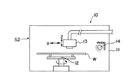
ここで、表面検査装置10の一例について図3に基づいて説明すると、例えばウエハWの搬送口(図示せず)を備えた筐体11と、この筐体11内に設けられ、ウエハWを水平に支持してその向きを調整できるように構成された回転載置台12と、この回転載置台12上のウエハWの表面を撮像するX,Y,Z方向(Y方向はX,Z方向に垂直な方向であって、紙面に対して垂直な方向)に移動自在なCCDカメラ13と、照明手段14とを備えている。
そして、このCCDカメラ13で得られたウエハWの画像をデータ処理部であるコンピュータ4にて解析することによって検査を行なうように構成されている。なおCCDカメラ13は固定されていて、ウエハWの載置台12側がX,Y,Z方向に移動できる構成であってもよい。また、第一の検査・測定ステーションS2の空いたスペースにコンピュータを備え(図示せず)、ウエハWの画像データの処理の一部を行うようにしても良い。
【0028】
次に、処理ステーションS3について説明すると、この処理ステーションS3はカセットステーションS1のカセットの配列方向と略直交する方向に、カセットステーションS1に接続して設けられている。そして、例えば2個の基板処理部をなす現像ユニット20(20A,20B)と、2個の基板処理部をなす塗布ユニット21(21A,21B)と、例えば2個の第一、第二の棚ユニットR1、R2と、例えば1個の基板搬送手段22と、第二の検査・測定ステーションS6とを備えている。この第二の検査・測定ステーションS6には、ウエハW上に形成されたパターンの線幅を測定する線幅測定装置23が配置されている。
【0029】
そして、この基板搬送手段22によって、カセットステーションS1との間でウエハWの受け渡しを行うと共に、インターフェイスステーションS4との間でウエハWの受け渡し行うために、第一、第二の棚ユニットR1、R2中にそれぞれ受け渡し台を備えた受け渡し部43が配置されている。
また、この基板搬送手段22によって、ウエハWにレジスト液を塗布する塗布ユニット21(21A,21B)と、ウエハWの現像処理を行う現像ユニット20(20A,20B)と、これらの処理の前後にウエハWを所定の温度に加熱し、冷却する処理をする第一、第二の棚ユニットR1、R2と、更には基板上に形成されたパターンの線幅を測定する線幅測定装置23との間を、ウエハWが搬送されるように構成されている。
【0030】
このような処理ステーションS3のレイアウトの一例について説明すると、例えばカセットステーションS1から奥を見て例えば右側には現像ユニット20や塗布ユニット21等を備えた処理ユニットが2段に亘って設けられている。
なお、以降の説明では、カセットステーションS1側を手前側、露光装置S5側を奥側として述べることにする。
【0031】
また、カセットステーションS1から見て(図1の矢印A方向からみて)、処理ステーションS3の右側には、現像ユニット20、塗布ユニット21が配置されている。また、処理ステーションS3の中央部には、第一、第二の棚ユニットR1、R2と、第一の棚ユニットR1および第二の棚ユニットR2との間でウエハWを受け渡しするための、例えば昇降自在、左右、前後に移動自在かつ鉛直軸まわりに回転自在に構成された基板搬送手段22が設けられている。なお、この基板搬送手段22のカセットステーションS1側から見て手前側には第一の棚ユニットR1、奥側には第二の棚ユニットR2が配置されている。
【0032】
そしてまた、基板搬送手段22のカセットステーションS1側から見て左側には第二の検査・測定ステーションS6が配置され、この第二の検査・測定ステーションS6には線幅測定装置23が配置されている。したがって、前記第一の検査・測定ステーションS2と第二の検査・測定ステーションS6は、塗布・現像処理装置の同一側に配置されている。なお、図2には便宜上、基板搬送手段22は省略してある。
【0033】
以上のように、前記処理ステーションS3は、中心部に配置された基板を搬送する基板搬送手段22と、前記カセットステーション側に配置された第一の棚ユニットR1と、前記基板搬送手段22を挟んで第一の棚ユニットR1に対向して配置された第二の棚ユニットR2と、前記基板搬送手段22を囲むように配置された前記第一、第二の棚ユニットR1、R2の配列方向と略直交した位置に配置された現像ユニット20、塗布ユニット21とを備えている。そして、前記検査・測定ステーションS6は、前記基板搬送手段22を囲むように現像ユニット20、塗布ユニット21に対向して配置されると共に、該検査・測定ステーションに検査・測定装置が配置されている。
【0034】
なお、前記検査・測定ステーションS6は、第一の棚ユニットR1及び第二の棚ユニットR2から離間して配置されている。
この検査測定装置は、一般的に周辺環境温度が例えば30℃以上になると検査測定装置の測定精度に悪影響を及ぼすため、後述するように加熱部を有する第一、第二の棚ユニットR1,R2に隣接して配置しないことが望ましい。
【0035】
ここで、線幅測定装置23の一例について図4に基づいて説明する。なお、図4(a)は線幅測定装置23の平面図であり、(b)は(a)に示したI−I断面図である。
図4に示すように、線幅測定装置23はウエハWの搬送口25aを備えた筐体25と、この筐体25内に設けられ、ウエハWを水平に支持してその向きを調整できるように構成された回転載置台26と、この回転載置台26上のウエハWに対して線幅測定装置23の上方に設けられた照明手段28からの光を入射し、反射した光を検出するX,Y,Z方向(Y方向はX,Z方向に垂直な方向であって、紙面に対して垂直な方向)に移動自在なレンズを備えた光学手段である顕微分分光光学系ユニット27と、筐体内部を排気するファン29と、このファン29の前面に配置されたフィルタ30とを備えている。
【0036】
また、前記顕微分分光光学系ユニット27は一端部にボールスクリュー部32が形成された支持部31に設けられている。前記支持部31の他端部にはガイド部33が形成され、ガイド棒34に沿って案内されるように形成されている。即ち、図示しないモータによってネジ軸35が回転することによって、X,Y方向に、顕微分分光光学系ユニット27が移動可能に形成されている。なお顕微分分光光学系ユニット27は固定されていて、ウエハWの載置台26側がX,Y,Z方向に移動できる構成であってもよい。
【0037】
更に、前記ファン29の排出口25bは、カセットステーションS1側から見て、線幅測定装置23の左側面に設けられている。即ち、排出口25bからの排気が、処理ステーションS3の内部に入り込まない位置に設けられている。
また、前記したようにファン29およびフィルタ30が形成されているため、顕微分分光光学系ユニット27を移動させた際、ボールスクリュー部32、ネジ軸35、ガイド部33、ガイド棒34から発生するパーティクルが処理装置内に侵入するのを防止できる。
【0038】
また,この線幅測定装置23は、顕微分分光光学系ユニット27によって得られた反射光を、データ処理部であるコンピュータ4にて解析することによって検査を行なうように構成されている。また、第二の検査・測定ステーションS6の空いたスペースにコンピュータを備え(図示せず)、得られたデータの解析、処理を行うようにしても良い。
【0039】
また、棚ユニットについて説明するが、第一、第二の棚ユニットR1,R2は略同一の構成を有するため、図5に第一の棚ユニットR1を代表して示し、図5に基づいて棚ユニットについて説明する。なお、この図5においては、基板搬送手段22を図示するため、第一の棚ユニットR1と現像ユニット20、塗布ユニット21との間が、拡げて図示されている。
【0040】
この第一、第二の棚ユニットR1,R2は、ウエハWを加熱するための加熱部40と、ウエハWを冷却するための冷却部41と、ウエハ表面を疎水化するための疎水化部42を備えている。
また、第一の棚ユニットR1においてはカセットステーションS1の受け渡しアーム3と処理ステーションS3の基板搬送手段22との間でウエハWの受け渡しを行なうための、一方第二の棚ユニットR2においては処理ステーションS3の基板搬送手段22と後述するインターフェイスステーションS4の搬送アーム60との間でウエハWの受け渡しを行なうための、受け渡し台を備えた受け渡し部43を備えている。
更に、第一の棚ユニットR1においてはウエハWの位置合わせを行なうためのアライメント部44とが縦に配列されている。
【0041】
また、図5に示されるように第二の検査・測定ステーションS6には、前記したように線幅測定装置23およびランプ等の照明手段28が配置されている。またこの線幅測定装置23の下部には、エレキユニット部50が設けられている。このエレキユニット部50には、線幅測定装置23、前記基板搬送手段22や後述する塗布ユニット21や現像ユニット20に用いられる部材、例えばこれらの駆動系の電源部や、これらの電力制御等を行うためのコントローラ、これらに電力を分配するための配電盤等の電気関係設備が収納されている。
【0042】
また、前記照明手段28の上部は空間部51となっている。この空間部にウエハWを加熱するための加熱部53を設ける場合には、図6に示すように断熱部材52を照明手段28の上部に配置し、その断熱部材52の上部に加熱部53を配置する。
このように配置することで、塗布・現像装置全体の専有面積の低減を図ることができると共に、処理のスループットを向上させることができる。また、図6のように加熱部53を複数段配置せず、線幅測定装置23から遠い上方の段のみに加熱部53を配置するような場合には、断熱部材52を省くこともできる。この場合、加熱部53と線幅測定装置23との間は、空間部(ブランク)である。
【0043】
なお、この加熱部53の処理温度は90℃乃至250℃であり、この加熱部53では、前記第一、第二の棚ユニットR1,R2における加熱部40の処理温度100℃乃至350℃よりも低い温度で処理される。このように加熱部40の処理温度よりも低い処理温度の加熱部53を配置したため、線幅測定装置23に与える熱の影響は小さくすることができる。
【0044】
上記したように、第二の検査・測定ステーションS6において、線幅測定装置23の下部には加熱部53のような処理部が設けられておらず、線幅測定装置23の下部に設けなければならないエレキユニット部50を除いて、線幅測定装置23は最も下部に設けられている。
このように、線幅測定装置23が第二検査・測定ステーションS6の下方に設けられているため、基板搬送手段22等から発生する振動を受けた場合であっても、第二の検査・測定ステーションS6の上方に配置されている場合に比べて、振動の影響を小さくすることができる。
【0045】
また、加熱部53を設ける場合、線幅測定装置23上方に加熱部53が配置されているため、加熱部53から生ずる熱の影響を少なくすることができる。即ち、加熱部53の熱によって温められた空気の大部分は上昇し、線幅測定装置23方向に下降する空気は少ない。また加熱部53と照明手段28との間に断熱部材が介装されているため、加熱部53からの伝熱による熱の影響を小さくすることができる。
【0046】
このように線幅測定装置23を配置することにより、振動、熱の影響を極力抑制しているため、精度の高い測定を行うことができると共に、その寿命を延ばすことができる。なお、同様に照明手段28のランプ等の寿命も延ばすことができる。
【0047】
また、現像ユニット20、塗布ユニット21は従来から用いられている一般的な現像ユニット20、塗布ユニット21を用いることができるため、詳細な説明は省略し、その概略を説明する。
現像ユニット20には、例えば、カップ内に真空吸着機能を有する回転自在なスピンチャック、処理液の吐出ノズル、処理液供給管、ノズルを水平移動させる支持アームが設けられている。このスピンチャックは昇降機構により昇降自在に構成されており、カップの上方側に位置しているときに、前記基板搬送手段22との間でウエハWの受け渡しが行なわれる。
【0048】
そして、ウエハWをカップの上方位置においてスピンチャックが受取ると、下降する。その後、スピンチャック上のウエハWの表面に吐出ノズルから現像液を吐出し、スピンチャックを半回転させることによりウエハW上に現像液の液盛りが行なわれ、現像液の液膜が形成されるようになっている。
【0049】
また塗布ユニット21は現像ユニット20とほぼ同一の構成であるが、塗布ユニット21は吐出ノズルが例えばウエハWのほぼ中心付近に処理液を供給するように構成され、スピンチャック上のウエハWの表面に吐出ノズルから処理液であるレジスト液を滴下し、スピンチャックを回転させてレジスト液をウエハW上に伸展させ塗布するようになっている。
【0050】
また、塗布ユニット21の下部には収納部54が設けられ、塗布ユニットや現像ユニットに用いられる部材、例えば、現像液、洗浄液等のケミカル材、駆動系の電源部や、これらの電力制御等を行なうためのコントローラ、これらに電力を分配するための配電盤等の電気関係の設備が収納されている。
【0051】
次に、この処理ステーションS3の隣に接続されたインターフェイスステーションS4について説明する。
このインターフェイスステーションS4の奥側には、レジスト膜が形成されたウエハWに対して露光を行なうための露光装置S5が接続され、このインターフェイスステーションS4には、処理ステーションS3と露光装置S5との間でウエハWの受け渡しを行なうための搬送アーム60が設けられている。
この搬送アーム60は、処理ステーションS3の第二の棚ユニットR2の受け渡し部43と露光装置S5との間でウエハWの受け渡しを行なうために、例えば昇降自在、左右、前後に移動自在かつ鉛直軸まわりに回転自在に構成されている。
【0052】
このインターフェイスステーションS4には、第三の検査・測定ステーションS7が設けられている。この第三の検査・測定ステーションS7には、レジスト膜の膜厚を測定する膜厚測定装置61が配置されている。
【0053】
また上述の膜厚測定装置61は、例えば図7に示すように、発光部と受光部とを備えた膜厚プローブ62を設け、ウエハに光を照射して反射率を求め、これをコンピュータで解析することにより膜厚が検出されるようになっている。
即ち、膜厚測定装置61は、ウエハWの搬送口を備えた筐体64と、この筐体64内に設けられ、ウエハWを水平に支持してその向きを調整できるように構成された回転載置台63と、この回転載置台63上に載置されたウエハ表面の膜厚を測定する膜厚プローブ62とを備えている。
そして、この膜厚プローブ62で得られたデータをデータ処理部であるコンピュータ4にて解析することによって測定を行なうように構成されている。なお膜厚プローブ62は固定されていて、ウエハWの載置台63側がX,Y,Z方向に移動できる構成であってもよい。また、インターフェイスステーションS4の空いたスペースにコンピュータを備え(図示せず)、得られたデータの処理の一部を行うようにしても良い。
【0054】
また、この第一乃至第三の検査測定ステーションS2、S6、S7は、独立して構成されている。即ち、図1及び図2に示すように、当該ステーションS2、S6、S7は壁部70,71,72により他の空間から区画され、ユニット化されている。
そのため、カセットステーションS1に隣接する前記壁部70には、第一の検査・測定ステーションS2の表面検査装置10に対してウエハWを受け渡すための受け渡し口(図示せず)が形成されている。また、処理ステーションS3における第二の検査測定ステーションS6の基板搬送手段22に隣接する前記壁部71には、第二の検査・測定ステーションS6の線幅測定装置23に対してウエハWを受け渡すための受け渡し口(図示せず)が形成されている。更に、インターフェイスステーションS4に隣接する前記壁部72には、第三の検査・測定ステーションS7の膜厚測定装置61に対してウエハWを受け渡すための受け渡し口(図示せず)が形成されている。
【0055】
こうして壁部70,71、72により区画された第一乃至第三の検査測定ステーションS2、S6、S7の背面側には、コンピュ−タ4に接続するための接続コードを導出するための開口部(図示せず)が設けられている。
このように第一乃至第三の検査測定ステーションS2、S6、S7をカセットステーションS1側から見て一方側に配置され、しかも接続コードを導出するための開口部が壁部70,71、72の背面側に設けられているため、コンピュータ4に接続し易く、煩雑にならない。
なお、本実施形態においては、コンピュータ4を塗布・現像装置本体とは離れた構成としているが、これに限らずS1〜S7のステーションの空いたスペースにコンピュータ4を組み込んで、操作パネル等を介して操作可能な構成とすることもできる。この場合、操作パネルを設ける位置は、装置本体の背面側が望ましい。
【0056】
また、壁部70,71、72により区画された第一乃至第三の検査測定ステーションS2、S6、S7の上部側には、フィルタユニットFが覆うように設けられている。これを第二の検査測定ステーションS6の場合について図8に基づいて説明する。なお、図8は図1に示すI−I線断面図である。
【0057】
図に示されるように、壁部71により区画された第二の検査測定ステーションS6にはフィルタユニットFが上部側を覆うように設けられ、エレキユニット部50、収納部54の下部側から回収される雰囲気が上昇排気系に排気される一方、一部が調整部をなすフィルタ装置75へと導入され、このフィルタ装置75にて清浄化され、所定の温度及び所定湿度に調整された空気が、前記フィルタユニットFを介して各部内にダウンフローとして吹き出されるようになっている。
前記フィルタユニットFは、例えば空気を清浄化するためのフィルタ、吸い込みファン等を備えており、前記フィルタ装置は、不純物を除去するための不純物除去部や、加熱機構及び加湿機構、空気を送出する送出部等を備えている。
【0058】
なお、前記壁部71と前記した線幅測定装置23の筐体25とを兼用することが好ましい。この場合、壁部71にファン29の排気口25bを壁部71に形成する必要がある。
【0059】
このように、検査・測定ステーションS2、S6、S7は、壁部70,71、72によって覆われているため温度影響を受けにくく、また検査測定ステーションS2、S6、S7を、フィルタ装置75で所定の温度・湿度に調整できるように構成するようにすれば、各検査測定装置は、周辺環境温度湿度が所定範囲に調整されるので、周囲の温度湿度の影響を受けることなく、精度の高い検査を行なうことができる。
【0060】
次に、実施の形態の作用について説明する。
先ず自動搬送ロボット(あるいは作業者)により例えば25枚のウエハWを収納したカセット2がカセットステージ1に搬入され、受け渡しアーム3によりカセット22内からウエハWが取り出される。なお、このウエハWは、すでにベアシリコンの膜厚が測定されているものが用いられる。また、ベアシリコンの膜厚が測定されていないウエハにあっては、ベアシリコンの膜厚も本発明の装置で測定することもできる。
このウエハWはカセットステージ1の受け渡しアーム3により処理ステーションS3の第一の棚ユニットR1の受け渡し部43に置かれ、次いで処理ステーションS3の基板搬送手段22により、第一、第二の棚ユニットR1,R2の疎水化部45→第一、第二の棚ユニットR1,R2の冷却部44→塗布ユニット42の経路で搬送され、ウエハ表面が疎水化された後、所定温度まで冷却されて温度調整が行なわれ、塗布ユニット42にて所定温度でレジスト液が塗布される。
【0061】
こうしてレジスト液が塗布されたウエハWは、基板搬送手段22、基板搬送手段3を介して、第一の検査測定ステーションS2の表面検査装置10に搬送され、レジストの塗布ムラ、スクラッチ、パーティクル等の表面検査が行われる。
その後、基板搬送手段3、基板搬送手段22を介して、第二の棚ユニットR2の受け渡し部46を介してインターフェイスステーションS4の搬送アーム60に受け渡され、膜厚測定装置61にてレジスト膜の膜厚が測定される。測定後のウエハWは、インターフェイスステーションS4の搬送アーム60を介して露光装置S5に搬送されて、露光が行なわれる。
【0062】
露光後のウエハWは露光装置S5→インターフェイスステーションS4の搬送アーム60→処理ステーションS3の第二の棚ユニットR2の受け渡し部46を介して処理ステーションS3に搬送され、ここで基板搬送手段22により第一、第二の棚ユニットR1,R2の加熱部40→第一、第二の棚ユニットR1,R2の冷却部44→現像ユニット41の経路で搬送され、所定の温度調整が行なわれたウエハWは現像ユニット41にて所定温度例えば現像液の塗布温度である23℃で現像処理される。
【0063】
その後、ウエハWは処理ステーションS3の基板搬送手段22により、第一、第二の棚ユニットR1,R2の加熱部40→第一、第二の棚ユニットR1,R2の冷却部44→第二の検査測定ステーションS6の経路で搬送される。
そして、第二の検査測定ステーションS6の線幅測定装置によって線幅が測定される。
測定後、処理ステーションS3の基板搬送手段22により、第二の検査測定ステーションS6から第一の棚ユニットR1の受け渡し部46の経路で搬送され、この受け渡し部46のウエハWは、カセットステーションS1の基板搬送手段3に受け取られる。
【0064】
そして、前記基板搬送手段3により第一の検査測定ステーションS2の表面検査装置10に搬送され、現像欠陥等の現像処理状態の検査が行なわれる。次いで所定の検査が行なわれたウエハWは、受け渡しアーム3より元のカセット2内に戻される。
【0065】
上述の実施形態では、検査測定ステーションを備えているため、レジストの塗布、露光、現像、検査を、共通のオペレータで監視することができるので、オペレータの省数化を図ることができる上、検査により何らかの欠陥が認められたときに、速やかに原因の特定や、原因排除のため、次のアクションを起こすことができる。
【0066】
さらに各ステーションS1、S3、S4と検査測定ステーションS2、S6、S7との間のウエハWの搬送は全て自動で行なわれるので、搬送作業の煩わしさがなくなり、基板処理から検査までのトータルの作業の簡便化を図ることができる。
またこれらのステーションS1乃至S7間のウエハWの搬送時間も短いので、前記基板処理から検査までのトータルの作業時間を短縮することができる上、処理の状態をリアルタイムで検査することができるので、より精度の高い検査を行なうことができ、さらに何らかの欠陥の早期発見等を図ることができる。
更にまた、検査測定ステーションS2、S6、S7における検査測定装置は、塗布・現像装置の内部に組み込まれるので、パーティクルを低減するための設備を共用できる。
【0067】
また、上記実施形態にあっては、各検査測定ステーションに一つの検査測定装置を配置した場合を示したが、同種あるいは異種の複数の検査測定装置を組み合わせて一つの検査測定ステーションを構成しても良い。
即ち、第一の検査測定ステーションに複数の表面検査装置を、第二の検査測定ステーションに複数の線幅測定装置を、第三の検査測定ステーションに複数の線幅測定装置を配置しても良い。また、第一の検査測定ステーションに表面検査装置と膜厚測定装置を、第二の検査測定ステーションに線幅測定装置と表面検査装置を、第三の検査測定ステーションに線幅測定装置と膜厚測定装置を配置しても良い。
このように、同一のステーション内に同種あるいは異種の複数の検査測定装置を配置することによって、ウエハWに対して同種あるいは異種の複数の検査を行なうことができ、検査測定に要するトータルの時間も短縮される。
【0068】
また、本実施形態においては、表面検査装置、線幅測定装置、膜厚測定装置の全てを備えた塗布・現像装置の例について説明したが、これに限らず各検査測定ステーションの検査・測定装置を同一の検査測定装置としてもよい。即ち、第一乃至第三の検査測定ステーションの検査測地装置を、たとえば表面検査装置としても良い。
【0069】
【発明の効果】
本発明にかかる基板処理装置によれば、熱、振動などの影響が小さく、高精度な検査・測定を行うことができると共に、基板処理から検査に亘る作業の簡便化と、時間の短縮とを図ることができる。
【図面の簡単な説明】
【図1】図1は、本発明にかかる一実施形態を示す平面概略図である。
【図2】図2は、図1に示した装置の斜視図である。
【図3】図3は、表面検査装置の概略構成図である。
【図4】図4は、線幅測定装置の概略平面図であって、(a)は平面図、(b)は(a)のI−I断面図である。
【図5】図5は、各ステーションの配置関係を示す図である。
【図6】図6は、第二検査・測定ステーションの配置図である。
【図7】図7は、膜厚測定装置の概略構成図である。
【図8】図8は、図1のI−I断面図である。
【図9】図9は、従来の基板処理装置を示す平面概略図である。
【符号の説明】
2 カセット
3 受け渡しアーム
4 コンピュータ
10 表面検査装置
20 現像ユニット
21 塗布ユニット
22 基板搬送手段
23 線幅測定装置
40 加熱部
43 受け渡し部
52 断熱部材
53 加熱部
60 搬送アーム
61 膜厚測定装置
70 壁部
71 壁部
72 壁部
S1 カセットステーション
S2 第一の検査・測定ステーション
S3 処理ステーション
S4 インターフェイスステーション
S5 露光装置
S6 第二の検査・測定ステーション
S7 第三の検査・測定ステーション
R1 第一の棚ユニット
R2 第二の棚ユニット[0001]
BACKGROUND OF THE INVENTION
The present invention includes an inspection / measurement apparatus that performs a coating process or a development process of a resist solution on a substrate such as a semiconductor wafer or a glass substrate for a liquid crystal display, and inspects and measures the processing state of these processes. The present invention relates to a substrate processing apparatus.
[0002]
[Prior art]
In photolithography technology in the manufacturing process of semiconductor devices, a resist is applied to the surface of a semiconductor wafer (hereinafter referred to as a wafer), this coated resist is exposed to a predetermined pattern, and further developed to form a resist film having a predetermined pattern. The Such a series of processes is performed by a system in which an exposure apparatus is connected to a coating / developing apparatus.
[0003]
FIG. 9 is a plan view showing a conventional example of such an apparatus, which is performed by a pattern forming system in which an
[0004]
In this system, the wafer W carried into the
In this way, when the processed wafer W is stored in the carrier C, the carrier C is unloaded from the
[0005]
Then, the wafer W determined to be acceptable is sent to the next process, but the wafer W determined to be unacceptable is sent to a cleaning unit (not shown) to dissolve and remove the resist, and before the application and development are performed. Return to. Then, this wafer is sent again to the development system, and the same processing is performed again.
[0006]
[Problems to be solved by the invention]
By the way, in the pattern forming system described above, since the inspection / measurement apparatus is installed separately from the coating / development apparatus, a separate operator is required to confirm the operation of the inspection / measurement apparatus. Further, since the wafer W has to be transferred between the coating / developing apparatus and the inspection / measurement apparatus, the transfer operation is troublesome, and it becomes a considerable problem when 100% inspection of the wafer W is required. In addition, since it takes time to carry, it is difficult to inspect the state of the development processing in real time, and there is a problem that new equipment is required to reduce particles in the environment where the inspection / measurement apparatus is placed.
[0007]
For this reason, the present inventors are considering incorporating an inspection / measurement apparatus into the coating / developing apparatus. At this time, in order to utilize the current layout of the coating / developing apparatus, it is conceivable to connect an inspection / measurement apparatus beside the cassette station.
[0008]
However, it may be necessary to inspect not only after development but also after application of the resist solution. Simply connecting an inspection / measurement device next to the cassette station will reduce the throughput, and the processing status in real time. There was a problem that it was difficult to inspect. Further, when the inspection / measurement apparatus is incorporated in the coating / developing apparatus, it is necessary to prevent the inspection / measurement apparatus from being affected by the heat from the heating unit (heat treatment apparatus) in the processing station. Furthermore, when the inspection / measurement device is incorporated in the coating / developing device, it is necessary to prevent the inspection / measurement device from being affected by vibrations generated from the transfer arm or the like.
[0009]
The present invention has been made in order to solve the above technical problem, and by connecting the inspection / measurement apparatus to a cassette station, a processing station, etc. to constitute a substrate processing apparatus, the influence of heat, vibration, etc., can be achieved. It is an object of the present invention to provide a substrate processing apparatus that can perform inspection / measurement without receiving it, and that simplifies work from substrate processing to inspection and shortens time.
[0010]
[Means for Solving the Problems]
The present invention has been made to achieve the above object, and a substrate processing apparatus according to the present invention includes a cassette stage on which a substrate cassette storing a plurality of substrates is placed, and a substrate placed on the cassette stage. A cassette station including a transfer means for transferring a substrate to the cassette; a processing station connected to the cassette station for performing a predetermined process on the substrate conveyed from the cassette station; and connected to the processing station. The cassette station comprising: an interface station that transports the substrate transported from the processing station to another processing apparatus; and first to third inspection / measurement stations that inspect and measure the processing state of the substrate in the processing station. Connected to the first inspection / measurement station The second test and measurement station is connected to the processing station, the third inspection and measurement station is connected to the interface station,All inspection / measurement stations of the first to third inspection / measurement stations are arranged on one side when viewed from the cassette station, and a second inspection / measurement station connected to the processing station is the processing station. Is disposed so as to face the resist coating processing unit and the development processing unit provided inIt is characterized by that.
[0011]
With this configuration, compared to the case where an inspection / measurement station is placed next to the cassette station, the inspection / measurement station can be used properly according to the processing state of the substrate, improving throughput and processing. Can be inspected in real time. That is, the work from the substrate processing to the inspection can be simplified and the time can be shortened.
[0012]
Also,The first to third inspection / measurement stations are provided on one side when viewed from the cassette station.Because on that sideOperators can be arranged, and operator operations are facilitated.
This substrate processing apparatus is suitable for a substrate processing apparatus in which processing at the processing station is resist coating and development processing, and the other processing apparatus is an exposure apparatus.
[0013]
Further, it is preferable that the inspection / measurement devices arranged in the first to third inspection / measurement stations provided on one side as viewed from the cassette station are connected to one computer.
Thus, since the first to third inspection / measurement stations are provided on one side when viewed from the cassette station, it is easy to connect to one computer, and the inspection / measurement data is concentrated. In addition, the result can be immediately fed back to the processing device of the processing station.
[0014]
The inspection / measurement apparatus disposed in the first to third inspection / measurement stations is preferably any of a surface inspection apparatus, a film thickness measurement apparatus, and a line width measurement apparatus.
[0015]
Preferably, the inspection / measurement apparatus disposed at the first inspection / measurement station is a surface inspection apparatus, and the inspection / measurement apparatus disposed at the second inspection / measurement station is a line width measurement. It is preferable that the inspection / measurement apparatus disposed in the third inspection / measurement station is a film thickness measurement apparatus.
Further, it is desirable that a plurality of the same or different devices selected from the surface inspection device, the film thickness measuring device, and the line width measuring device are arranged in the first to third inspection / measurement stations. As described above, by arranging a plurality of inspection / measurement devices of the same type or different types in the same station, a plurality of inspections of the same type or different types can be performed on the substrate, and the total time required for the inspection / measurement can be shortened. Is done.
[0016]
In addition, the present invention has been made to achieve the above object, and a substrate processing apparatus according to the present invention is mounted on a cassette stage on which a substrate cassette storing a plurality of substrates is mounted, and on this cassette stage. A cassette station including a transfer means for transferring the substrate to the substrate cassette, a processing station connected to the cassette station and performing a predetermined process on the substrate conveyed from the cassette station, and the processing station. An interface station for transferring a substrate transferred from the processing station to another processing apparatus, and an inspection / measurement station for inspecting / measuring the processing state of the substrate in the processing station, Substrate transporter that transports the substrate placed in the section A first shelf unit having a heating unit disposed on the cassette station side, and a second shelf unit having a heating unit disposed to face the first shelf unit across the substrate transfer means, The first and second shelf units so as to surround the substrate transfer meansAt a position approximately perpendicular to the direction ofThe inspection / measurement station is disposed to face the processing unit so as to surround the substrate transfer means, andA heating unit is disposed above the inspection / measurement station, an inspection / measurement device is disposed below the heating unit, and a processing temperature of the heating unit disposed in the inspection / measurement station is equal to that of the first and second shelf units. It is set lower than the processing temperature of the heating unitIt is characterized by that.
[0017]
As described above, the inspection / measurement station is provided with the inspection / measurement device facing the processing unit so as to surround the substrate transfer means of the processing station, so that the processing state can be inspected / measured quickly. It is possible to simplify the work from the substrate processing to the inspection and to shorten the time.A heating unit is disposed above the inspection / measurement station, and an inspection / measurement device is disposed below the heating unit. For this reason, compared with the case where the heating unit is arranged below the inspection / measurement apparatus, the inspection / measurement apparatus can suppress the influence of heat from the heating unit. Further, by arranging the inspection / measurement device below the inspection / measurement station, it is possible to reduce the influence of vibration generated from the substrate transfer means or the like.
The processing temperature of the heating unit disposed above the inspection / measurement device is set lower than the processing temperature of the heating unit of the shelf unit.
[0018]
Here, it is preferable that the inspection / measurement station is disposed apart from the first shelf unit and the second shelf unit.
Since they are spaced apart in this way, it is possible to suppress the influence of heat from the heating portions of the first and second shelf units.
[0019]
In addition, it is desirable that an electric unit part of the inspection / measurement apparatus is disposed at the lowermost part of the inspection / measurement station, and an inspection / measurement apparatus is disposed above the electric unit part.
[0020]
Furthermore, it is desirable that a heat insulating member is disposed between the inspection / measurement apparatus and the heating unit, which is disposed in the inspection / measurement station, and is insulated between the inspection / measurement apparatus and the heating unit. When a member is placedThe influence of heat from the heating unit can be reduced.
The processing temperature of the heating unit disposed above the inspection / measurement device is set lower than the processing temperature of the heating unit of the shelf unit.
[0021]
Furthermore, it is desirable that the inspection / measurement apparatus is provided with a fan and a filter for exhausting the inside of the apparatus, so that particles generated from the drive unit and the like can be captured and maintained in a clean state. it can.
[0022]
The inspection / measurement device is preferably a line width measurement device. Since the line width measuring device is arranged as the inspection / measurement device, the line width of the developed pattern can be quickly inspected / measured, and the work from substrate processing to inspection can be simplified and time-consuming. Can be shortened.
[0023]
DETAILED DESCRIPTION OF THE INVENTION
Embodiments in which the present invention is applied to a substrate coating / developing apparatus will be described below. 1 and 2 show a basic configuration of a substrate processing apparatus (coating / developing apparatus) to which the present invention is applied. FIG. 1 shows a state seen through from above, and FIG. 2 shows a perspective view.
[0024]
In the figure, S1 is a cassette station, S2 is a first inspection / measurement station for performing predetermined inspection / measurement on the wafer W, and S3 is substrate processing such as resist coating processing and development processing on the wafer W. S4 is an interface station, S5 is an exposure apparatus, S6 is a second inspection / measurement station for performing predetermined inspection / measurement on the wafer W, and S7 is similar to S2 and S6. This is a third inspection / measurement station for performing predetermined inspection / measurement on the wafer W.
[0025]
The cassette station S1 includes a cassette stage 1 on which, for example, four wafer cassettes (hereinafter referred to as “cassettes”) 2 storing a plurality of substrates, for example, 25 wafers W, a
The
[0026]
The first inspection / measurement station S2 is connected to the cassette station S1 in parallel to the arrangement direction of the
This
[0027]
Here, an example of the
The inspection is performed by analyzing the image of the wafer W obtained by the
[0028]
Next, the processing station S3 will be described. The processing station S3 is connected to the cassette station S1 in a direction substantially orthogonal to the cassette arrangement direction of the cassette station S1. For example, the developing unit 20 (20A, 20B) that forms two substrate processing units, the coating unit 21 (21A, 21B) that forms two substrate processing units, and two first and second shelves, for example. Units R1, R2, for example, one substrate transport means 22, and a second inspection / measurement station S6 are provided. In the second inspection / measurement station S6, a line
[0029]
The substrate transfer means 22 transfers the wafer W to and from the cassette station S1 and also transfers the wafer W to and from the interface station S4 in order to transfer the wafer W to the first and second shelf units R1 and R2. The delivery part 43 provided with the delivery stand in each is arrange | positioned.
Further, the substrate transport means 22 applies a coating unit 21 (21A, 21B) for applying a resist solution to the wafer W, a developing unit 20 (20A, 20B) for developing the wafer W, and before and after these processes. The first and second shelf units R1 and R2 that perform a process of heating and cooling the wafer W to a predetermined temperature, and a line
[0030]
An example of the layout of such a processing station S3 will be described. For example, when viewed from the back of the cassette station S1, processing units including a developing
In the following description, the cassette station S1 side is referred to as the front side, and the exposure apparatus S5 side is referred to as the back side.
[0031]
Further, when viewed from the cassette station S1 (as viewed from the direction of arrow A in FIG. 1), a developing
[0032]
In addition, a second inspection / measurement station S6 is disposed on the left side when viewed from the cassette station S1 side of the substrate transfer means 22, and a line
[0033]
As described above, the processing station S3 sandwiches the
[0034]
The inspection / measurement station S6 is disposed apart from the first shelf unit R1 and the second shelf unit R2.
Since this inspection and measurement apparatus generally adversely affects the measurement accuracy of the inspection and measurement apparatus when the ambient environment temperature becomes, for example, 30 ° C. or higher, the first and second shelf units R1 and R2 having heating units as described later. It is desirable not to place it adjacent to.
[0035]
Here, an example of the line
As shown in FIG. 4, the line
[0036]
The microspectroscopy
[0037]
Further, the
Further, since the
[0038]
The line
[0039]
Further, the shelf unit will be described. Since the first and second shelf units R1 and R2 have substantially the same configuration, the first shelf unit R1 is shown as a representative in FIG. The unit will be described. In FIG. 5, the space between the first shelf unit R <b> 1, the developing
[0040]
The first and second shelf units R1 and R2 include a
In the first shelf unit R1, the wafer W is transferred between the
Further, in the first shelf unit R1, an
[0041]
Further, as shown in FIG. 5, the line
[0042]
The upper part of the illumination means 28 is a
By arranging in this way, the area occupied by the entire coating / developing apparatus can be reduced, and the throughput of processing can be improved. Further, when the
[0043]
The processing temperature of the
[0044]
As described above, in the second inspection / measurement station S <b> 6, a processing unit such as the
As described above, since the line
[0045]
Further, when the
[0046]
By arranging the line
[0047]
Further, since the developing
The developing
[0048]
When the spin chuck receives the wafer W at the upper position of the cup, the wafer W is lowered. Thereafter, the developer is discharged from the discharge nozzle onto the surface of the wafer W on the spin chuck, and the spin chuck is half-rotated to deposit the developer on the wafer W, thereby forming a liquid film of the developer. It is like that.
[0049]
The
[0050]
In addition, a
[0051]
Next, the interface station S4 connected next to the processing station S3 will be described.
An exposure apparatus S5 for exposing the wafer W on which the resist film is formed is connected to the back side of the interface station S4. The interface station S4 is connected between the processing station S3 and the exposure apparatus S5. A
The
[0052]
The interface station S4 is provided with a third inspection / measurement station S7. In the third inspection / measurement station S7, a film
[0053]
Further, the film
That is, the film
And it is comprised so that the data obtained with this
[0054]
In addition, the first to third inspection and measurement stations S2, S6, and S7 are configured independently. That is, as shown in FIGS. 1 and 2, the stations S2, S6, and S7 are partitioned from other spaces by the
Therefore, a delivery port (not shown) for delivering the wafer W to the
[0055]
In this way, on the back side of the first to third inspection and measurement stations S2, S6, and S7 divided by the
As described above, the first to third inspection / measurement stations S2, S6, and S7 are arranged on one side when viewed from the cassette station S1, and the openings for leading out the connection cords are formed in the
In the present embodiment, the
[0056]
A filter unit F is provided on the upper side of the first to third inspection and measurement stations S2, S6, and S7 defined by the
[0057]
As shown in the figure, a filter unit F is provided to cover the upper side of the second inspection / measurement station S6 defined by the
The filter unit F includes, for example, a filter for cleaning air, a suction fan, and the like, and the filter device sends out an impurity removing unit for removing impurities, a heating mechanism and a humidifying mechanism, and air. It has a sending part.
[0058]
In addition, it is preferable that the
[0059]
As described above, the inspection / measurement stations S2, S6, and S7 are covered with the
[0060]
Next, the operation of the embodiment will be described.
First, a
This wafer W is placed on the transfer section 43 of the first shelf unit R1 of the processing station S3 by the
[0061]
The wafer W thus coated with the resist solution is transferred to the
Thereafter, the film is transferred to the
[0062]
The exposed wafer W is transferred to the processing station S3 via the exposure unit S5 → the
[0063]
Thereafter, the wafer W is heated by the substrate transfer means 22 of the processing station S3, the
Then, the line width is measured by the line width measuring device of the second inspection / measurement station S6.
After the measurement, the substrate is transferred by the substrate transfer means 22 of the processing station S3 from the second inspection / measurement station S6 along the path of the transfer section 46 of the first shelf unit R1, and the wafer W of the transfer section 46 is transferred from the cassette station S1. It is received by the substrate transfer means 3.
[0064]
Then, the substrate is conveyed to the
[0065]
In the above-described embodiment, since the inspection and measurement station is provided, the resist application, exposure, development, and inspection can be monitored by a common operator, so that the number of operators can be saved and the inspection can be performed. When any defect is recognized, the following actions can be taken to quickly identify the cause and eliminate the cause.
[0066]
Furthermore, since the transfer of the wafer W between each of the stations S1, S3, S4 and the inspection / measurement stations S2, S6, S7 is automatically performed, the trouble of the transfer work is eliminated, and the total work from the substrate processing to the inspection is performed. Can be simplified.
Also, since the transfer time of the wafer W between these stations S1 to S7 is short, the total work time from the substrate processing to the inspection can be shortened, and the processing state can be inspected in real time. Inspection with higher accuracy can be performed, and early detection of some defects can be achieved.
Furthermore, since the inspection / measurement apparatuses in the inspection / measurement stations S2, S6, and S7 are incorporated in the coating / developing apparatus, facilities for reducing particles can be shared.
[0067]
Further, in the above embodiment, the case where one inspection measuring device is arranged in each inspection measuring station is shown, but one inspection measuring station is configured by combining a plurality of same or different inspection measuring devices. Also good.
That is, a plurality of surface inspection devices may be arranged at the first inspection and measurement station, a plurality of line width measurement devices at the second inspection and measurement station, and a plurality of line width measurement devices at the third inspection and measurement station. . Also, a surface inspection device and a film thickness measurement device are provided at the first inspection and measurement station, a line width measurement device and a surface inspection device are provided at the second inspection and measurement station, and a line width measurement device and a film thickness are provided at the third inspection and measurement station. A measuring device may be arranged.
In this way, by arranging a plurality of inspection / measurement devices of the same type or different types in the same station, a plurality of inspections of the same type or different types can be performed on the wafer W, and the total time required for the inspection measurement is also increased. Shortened.
[0068]
In the present embodiment, the example of the coating / developing apparatus provided with all of the surface inspection apparatus, the line width measurement apparatus, and the film thickness measurement apparatus has been described. May be the same inspection and measurement device. That is, the inspection geodetic device of the first to third inspection / measurement stations may be a surface inspection device, for example.
[0069]
【The invention's effect】
According to the substrate processing apparatus of the present invention, the influence of heat, vibration, etc. is small, high-precision inspection / measurement can be performed, and work from substrate processing to inspection can be simplified and time can be reduced. Can be planned.
[Brief description of the drawings]
FIG. 1 is a schematic plan view showing an embodiment according to the present invention.
FIG. 2 is a perspective view of the apparatus shown in FIG.
FIG. 3 is a schematic configuration diagram of a surface inspection apparatus.
4A and 4B are schematic plan views of the line width measuring device, in which FIG. 4A is a plan view and FIG. 4B is a cross-sectional view taken along line II of FIG.
FIG. 5 is a diagram illustrating an arrangement relationship between stations.
FIG. 6 is a layout view of a second inspection / measurement station.
FIG. 7 is a schematic configuration diagram of a film thickness measuring apparatus.
FIG. 8 is a cross-sectional view taken along the line II in FIG.
FIG. 9 is a schematic plan view showing a conventional substrate processing apparatus.
[Explanation of symbols]
2 cassettes
3 Delivery arm
4 Computer
10 Surface inspection equipment
20 Development unit
21 Application unit
22 Substrate transfer means
23 Line width measuring device
40 Heating section
43 Delivery Department
52 Heat insulation member
53 Heating part
60 Transfer arm
61 Film thickness measuring device
70 wall
71 Wall
72 Wall
S1 cassette station
S2 First inspection / measurement station
S3 processing station
S4 interface station
S5 Exposure equipment
S6 Second inspection / measurement station
S7 Third inspection and measurement station
R1 first shelf unit
R2 Second shelf unit
Claims (13)
前記カセットステーションに第一の検査・測定ステーションが接続され、前記処理ステーションに第二の検査・測定ステーションが接続され、前記インターフェイスステーションに第三の検査・測定ステーションが接続され、
前記第一乃至第三の検査・測定ステーションのすべての検査・測定ステーションがカセットステーションから見て一方の側に配置され、
前記処理ステーションに接続された第二の検査・測定ステーションが、前記処理ステーションに設けられたレジスト塗布処理ユニットおよび現像処理ユニットに対向するように配置されていることを特徴とする基板処理装置。A cassette station including a cassette stage for mounting a substrate cassette containing a plurality of substrates, and a transfer means for transferring a substrate to the substrate cassette mounted on the cassette stage; and connected to the cassette station, A processing station that performs a predetermined process on a substrate transported from a cassette station, an interface station that is connected to the processing station and transports the substrate transported from the processing station to another processing apparatus, and a substrate in the processing station And first to third inspection / measurement stations for inspecting / measuring the processing state of
A first inspection / measurement station is connected to the cassette station, a second inspection / measurement station is connected to the processing station, and a third inspection / measurement station is connected to the interface station;
All the inspection / measurement stations of the first to third inspection / measurement stations are arranged on one side when viewed from the cassette station,
A substrate processing apparatus, wherein a second inspection / measurement station connected to the processing station is arranged to face a resist coating processing unit and a development processing unit provided in the processing station.
前記処理ステーションは、その中心部に配置された基板を搬送する基板搬送手段と、前記カセットステーション側に配置された加熱部を有する第一の棚ユニットと、前記基板搬送手段を挟んで第一の棚ユニットに対向して配置された加熱部を有する第二の棚ユニットと、前記基板搬送手段を囲むように前記第一、第二の棚ユニットの配列方向と略直交した位置に配置された処理ユニットとを含み、
前記検査・測定ステーションは、前記基板搬送手段を囲むように処理ユニットに対向して配置されると共に、該検査・測定ステーションの上方に加熱部、その下方に検査・測定装置が配置され、
さらに、前記検査・測定ステーションに配置された加熱部の処理温度が、前記第一、第二の棚ユニットの加熱部の処理温度より低く設定されていることを特徴とする基板処理装置。A cassette station including a cassette stage for mounting a substrate cassette containing a plurality of substrates, and a transfer means for transferring a substrate to the substrate cassette mounted on the cassette stage; and connected to the cassette station, A processing station that performs a predetermined process on a substrate transported from a cassette station, an interface station that is connected to the processing station and transports the substrate transported from the processing station to another processing apparatus, and a substrate in the processing station An inspection / measurement station that inspects / measures the processing state of
The processing station includes a substrate transport unit that transports a substrate disposed at a central portion thereof, a first shelf unit having a heating unit disposed on the cassette station side, and a first shelf across the substrate transport unit. A second shelf unit having a heating unit disposed opposite to the shelf unit, and a process disposed at a position substantially orthogonal to the arrangement direction of the first and second shelf units so as to surround the substrate transfer means. Including units,
The inspection / measurement station is disposed so as to face the processing unit so as to surround the substrate transfer means, a heating unit is disposed above the inspection / measurement station, and an inspection / measurement apparatus is disposed below the heating unit.
Furthermore, the processing temperature of the heating part arrange | positioned at the said test | inspection / measurement station is set lower than the processing temperature of the heating part of said 1st, 2nd shelf unit, The substrate processing apparatus characterized by the above-mentioned.
Priority Applications (1)
| Application Number | Priority Date | Filing Date | Title |
|---|---|---|---|
| JP2001345005A JP3761081B2 (en) | 2001-11-09 | 2001-11-09 | Substrate processing equipment |
Applications Claiming Priority (1)
| Application Number | Priority Date | Filing Date | Title |
|---|---|---|---|
| JP2001345005A JP3761081B2 (en) | 2001-11-09 | 2001-11-09 | Substrate processing equipment |
Publications (2)
| Publication Number | Publication Date |
|---|---|
| JP2003151878A JP2003151878A (en) | 2003-05-23 |
| JP3761081B2 true JP3761081B2 (en) | 2006-03-29 |
Family
ID=19158428
Family Applications (1)
| Application Number | Title | Priority Date | Filing Date |
|---|---|---|---|
| JP2001345005A Expired - Fee Related JP3761081B2 (en) | 2001-11-09 | 2001-11-09 | Substrate processing equipment |
Country Status (1)
| Country | Link |
|---|---|
| JP (1) | JP3761081B2 (en) |
Families Citing this family (5)
| Publication number | Priority date | Publication date | Assignee | Title |
|---|---|---|---|---|
| JP4342921B2 (en) * | 2003-12-09 | 2009-10-14 | 東京エレクトロン株式会社 | Substrate processing apparatus control method and substrate processing apparatus |
| TWI550686B (en) | 2011-11-04 | 2016-09-21 | 東京威力科創股份有限公司 | Substrate treatment system, substrate delivery method, and computer memory medium |
| TWI524456B (en) | 2011-11-04 | 2016-03-01 | 東京威力科創股份有限公司 | Substrate treatment system, substrate delivery method, program, and computer memory medium |
| JP5702263B2 (en) * | 2011-11-04 | 2015-04-15 | 東京エレクトロン株式会社 | Substrate processing system, substrate transfer method, program, and computer storage medium |
| JP6863114B2 (en) | 2017-06-16 | 2021-04-21 | 東京エレクトロン株式会社 | Substrate processing equipment, substrate processing method and storage medium |
Family Cites Families (5)
| Publication number | Priority date | Publication date | Assignee | Title |
|---|---|---|---|---|
| JP3342828B2 (en) * | 1997-01-30 | 2002-11-11 | 東京エレクトロン株式会社 | Resist coating and developing apparatus and resist coating and developing method |
| JP3455458B2 (en) * | 1999-02-01 | 2003-10-14 | 東京エレクトロン株式会社 | Coating and developing apparatus and substrate recycling system in coating and developing processing |
| JP4021138B2 (en) * | 1999-10-19 | 2007-12-12 | 東京エレクトロン株式会社 | Substrate processing equipment |
| JP3589406B2 (en) * | 1999-10-25 | 2004-11-17 | 東京エレクトロン株式会社 | Substrate processing system |
| JP3523819B2 (en) * | 1999-12-10 | 2004-04-26 | 東京エレクトロン株式会社 | Substrate processing equipment |
-
2001
- 2001-11-09 JP JP2001345005A patent/JP3761081B2/en not_active Expired - Fee Related
Also Published As
| Publication number | Publication date |
|---|---|
| JP2003151878A (en) | 2003-05-23 |
Similar Documents
| Publication | Publication Date | Title |
|---|---|---|
| KR100780133B1 (en) | Substrate processing apparatus and substrate processing method | |
| US8477301B2 (en) | Substrate processing apparatus, substrate processing system and inspection/periphery exposure apparatus | |
| US9508573B2 (en) | Substrate processing apparatus and substrate processing method | |
| JP3916468B2 (en) | Substrate processing apparatus and substrate processing method | |
| US7955011B2 (en) | Coating and developing apparatus, substrate processing method, and storage medium | |
| US8863373B2 (en) | Apparatus and method of application and development | |
| JP4069081B2 (en) | Position adjustment method and substrate processing system | |
| JP4004248B2 (en) | Substrate processing apparatus and substrate inspection method | |
| JP3943828B2 (en) | Coating, developing device and pattern forming method | |
| JP3679690B2 (en) | Substrate processing equipment | |
| JP4298238B2 (en) | Substrate processing apparatus and substrate processing system | |
| KR200487281Y1 (en) | Apparatus for examining substrate | |
| JP3801849B2 (en) | Substrate processing apparatus and method | |
| JP3761081B2 (en) | Substrate processing equipment | |
| JP4142702B2 (en) | Substrate processing apparatus and substrate processing system | |
| JP3612265B2 (en) | Coating and developing equipment | |
| JP3878441B2 (en) | Substrate processing equipment | |
| JP2005229131A (en) | Application and development apparatus | |
| JP3811409B2 (en) | Processing equipment | |
| JPH11220005A (en) | Wafer processing system | |
| JP2003037043A (en) | Substrate processing apparatus and substrate processing system | |
| JP2006344986A (en) | Coating and development device and pattern forming method | |
| JP5680731B2 (en) | Substrate processing apparatus and inspection peripheral exposure system | |
| JP2003100836A (en) | Substrate treatment system |
Legal Events
| Date | Code | Title | Description |
|---|---|---|---|
| A977 | Report on retrieval |
Free format text: JAPANESE INTERMEDIATE CODE: A971007 Effective date: 20050422 |
|
| A131 | Notification of reasons for refusal |
Free format text: JAPANESE INTERMEDIATE CODE: A131 Effective date: 20050428 |
|
| A521 | Written amendment |
Free format text: JAPANESE INTERMEDIATE CODE: A523 Effective date: 20050621 |
|
| TRDD | Decision of grant or rejection written | ||
| A01 | Written decision to grant a patent or to grant a registration (utility model) |
Free format text: JAPANESE INTERMEDIATE CODE: A01 Effective date: 20060105 |
|
| A61 | First payment of annual fees (during grant procedure) |
Free format text: JAPANESE INTERMEDIATE CODE: A61 Effective date: 20060105 |
|
| R150 | Certificate of patent or registration of utility model |
Free format text: JAPANESE INTERMEDIATE CODE: R150 |
|
| FPAY | Renewal fee payment (event date is renewal date of database) |
Free format text: PAYMENT UNTIL: 20120120 Year of fee payment: 6 |
|
| FPAY | Renewal fee payment (event date is renewal date of database) |
Free format text: PAYMENT UNTIL: 20150120 Year of fee payment: 9 |
|
| LAPS | Cancellation because of no payment of annual fees |