KR900004197B1 - A.c. solid state relay circuit and structure - Google Patents
A.c. solid state relay circuit and structure Download PDFInfo
- Publication number
- KR900004197B1 KR900004197B1 KR1019830006040A KR830006040A KR900004197B1 KR 900004197 B1 KR900004197 B1 KR 900004197B1 KR 1019830006040 A KR1019830006040 A KR 1019830006040A KR 830006040 A KR830006040 A KR 830006040A KR 900004197 B1 KR900004197 B1 KR 900004197B1
- Authority
- KR
- South Korea
- Prior art keywords
- region
- anode
- conductivity type
- base
- thyristor
- Prior art date
Links
- 239000007787 solid Substances 0.000 title claims description 17
- 230000001960 triggered effect Effects 0.000 claims abstract description 3
- 239000000758 substrate Substances 0.000 claims description 39
- 239000003990 capacitor Substances 0.000 claims description 37
- 229910021420 polycrystalline silicon Inorganic materials 0.000 claims description 15
- 229920005591 polysilicon Polymers 0.000 claims description 15
- 238000000034 method Methods 0.000 claims description 14
- VYPSYNLAJGMNEJ-UHFFFAOYSA-N Silicium dioxide Chemical compound O=[Si]=O VYPSYNLAJGMNEJ-UHFFFAOYSA-N 0.000 claims description 12
- 230000001052 transient effect Effects 0.000 claims description 10
- 230000005855 radiation Effects 0.000 claims description 9
- 150000005690 diesters Chemical class 0.000 claims description 8
- 230000035945 sensitivity Effects 0.000 claims description 8
- 239000000463 material Substances 0.000 claims description 7
- 238000009826 distribution Methods 0.000 claims description 6
- 238000007667 floating Methods 0.000 claims description 6
- 230000003287 optical effect Effects 0.000 claims description 6
- 239000004065 semiconductor Substances 0.000 claims description 6
- 235000012239 silicon dioxide Nutrition 0.000 claims description 6
- 239000000377 silicon dioxide Substances 0.000 claims description 6
- 238000009792 diffusion process Methods 0.000 claims description 5
- 238000010304 firing Methods 0.000 claims description 4
- 206010034960 Photophobia Diseases 0.000 claims description 3
- 239000000969 carrier Substances 0.000 claims description 3
- 239000000919 ceramic Substances 0.000 claims description 3
- 208000013469 light sensitivity Diseases 0.000 claims description 3
- 230000003071 parasitic effect Effects 0.000 claims description 3
- 230000004044 response Effects 0.000 claims description 3
- 239000010409 thin film Substances 0.000 claims description 2
- 230000005284 excitation Effects 0.000 claims 1
- 239000012212 insulator Substances 0.000 claims 1
- XUIMIQQOPSSXEZ-UHFFFAOYSA-N Silicon Chemical compound [Si] XUIMIQQOPSSXEZ-UHFFFAOYSA-N 0.000 description 8
- 230000001939 inductive effect Effects 0.000 description 8
- 229910052710 silicon Inorganic materials 0.000 description 8
- 239000010703 silicon Substances 0.000 description 8
- 238000001465 metallisation Methods 0.000 description 7
- 229910052751 metal Inorganic materials 0.000 description 6
- 239000002184 metal Substances 0.000 description 6
- 229910052782 aluminium Inorganic materials 0.000 description 4
- XAGFODPZIPBFFR-UHFFFAOYSA-N aluminium Chemical compound [Al] XAGFODPZIPBFFR-UHFFFAOYSA-N 0.000 description 4
- PNEYBMLMFCGWSK-UHFFFAOYSA-N aluminium oxide Inorganic materials [O-2].[O-2].[O-2].[Al+3].[Al+3] PNEYBMLMFCGWSK-UHFFFAOYSA-N 0.000 description 4
- 238000010586 diagram Methods 0.000 description 4
- 230000008569 process Effects 0.000 description 4
- WYTGDNHDOZPMIW-RCBQFDQVSA-N alstonine Natural products C1=CC2=C3C=CC=CC3=NC2=C2N1C[C@H]1[C@H](C)OC=C(C(=O)OC)[C@H]1C2 WYTGDNHDOZPMIW-RCBQFDQVSA-N 0.000 description 3
- 230000005684 electric field Effects 0.000 description 3
- 230000001965 increasing effect Effects 0.000 description 3
- 239000011574 phosphorus Substances 0.000 description 3
- 229910052698 phosphorus Inorganic materials 0.000 description 3
- 239000000843 powder Substances 0.000 description 3
- 230000002829 reductive effect Effects 0.000 description 3
- ZOXJGFHDIHLPTG-UHFFFAOYSA-N Boron Chemical compound [B] ZOXJGFHDIHLPTG-UHFFFAOYSA-N 0.000 description 2
- OAICVXFJPJFONN-UHFFFAOYSA-N Phosphorus Chemical compound [P] OAICVXFJPJFONN-UHFFFAOYSA-N 0.000 description 2
- 206010034972 Photosensitivity reaction Diseases 0.000 description 2
- GWEVSGVZZGPLCZ-UHFFFAOYSA-N Titan oxide Chemical compound O=[Ti]=O GWEVSGVZZGPLCZ-UHFFFAOYSA-N 0.000 description 2
- 230000009471 action Effects 0.000 description 2
- 230000008901 benefit Effects 0.000 description 2
- 230000015572 biosynthetic process Effects 0.000 description 2
- 230000000903 blocking effect Effects 0.000 description 2
- 230000003750 conditioning effect Effects 0.000 description 2
- 239000004020 conductor Substances 0.000 description 2
- 238000000151 deposition Methods 0.000 description 2
- PCHJSUWPFVWCPO-UHFFFAOYSA-N gold Chemical compound [Au] PCHJSUWPFVWCPO-UHFFFAOYSA-N 0.000 description 2
- 239000010931 gold Substances 0.000 description 2
- 229910052737 gold Inorganic materials 0.000 description 2
- 230000000873 masking effect Effects 0.000 description 2
- 230000036211 photosensitivity Effects 0.000 description 2
- 230000009467 reduction Effects 0.000 description 2
- 230000000630 rising effect Effects 0.000 description 2
- OGIDPMRJRNCKJF-UHFFFAOYSA-N titanium oxide Inorganic materials [Ti]=O OGIDPMRJRNCKJF-UHFFFAOYSA-N 0.000 description 2
- ZXRRHFSTAFVGOC-UHFFFAOYSA-N [AlH3].[K] Chemical compound [AlH3].[K] ZXRRHFSTAFVGOC-UHFFFAOYSA-N 0.000 description 1
- 229910052796 boron Inorganic materials 0.000 description 1
- IRUJZVNXZWPBMU-UHFFFAOYSA-N cartap Chemical compound NC(=O)SCC(N(C)C)CSC(N)=O IRUJZVNXZWPBMU-UHFFFAOYSA-N 0.000 description 1
- 230000015556 catabolic process Effects 0.000 description 1
- 230000008859 change Effects 0.000 description 1
- 244000145845 chattering Species 0.000 description 1
- 239000011248 coating agent Substances 0.000 description 1
- 238000000576 coating method Methods 0.000 description 1
- 230000008021 deposition Effects 0.000 description 1
- 238000013461 design Methods 0.000 description 1
- 238000001514 detection method Methods 0.000 description 1
- 230000009977 dual effect Effects 0.000 description 1
- 238000005516 engineering process Methods 0.000 description 1
- 238000005530 etching Methods 0.000 description 1
- BHEPBYXIRTUNPN-UHFFFAOYSA-N hydridophosphorus(.) (triplet) Chemical compound [PH] BHEPBYXIRTUNPN-UHFFFAOYSA-N 0.000 description 1
- 238000005286 illumination Methods 0.000 description 1
- 238000002513 implantation Methods 0.000 description 1
- 230000001976 improved effect Effects 0.000 description 1
- 238000001802 infusion Methods 0.000 description 1
- 238000002347 injection Methods 0.000 description 1
- 239000007924 injection Substances 0.000 description 1
- 230000010354 integration Effects 0.000 description 1
- 238000005468 ion implantation Methods 0.000 description 1
- 150000002500 ions Chemical class 0.000 description 1
- 239000010977 jade Substances 0.000 description 1
- 238000005304 joining Methods 0.000 description 1
- 239000007788 liquid Substances 0.000 description 1
- 230000007257 malfunction Effects 0.000 description 1
- 238000004519 manufacturing process Methods 0.000 description 1
- 150000002739 metals Chemical class 0.000 description 1
- 239000000203 mixture Substances 0.000 description 1
- 238000012986 modification Methods 0.000 description 1
- 230000004048 modification Effects 0.000 description 1
- 229910021421 monocrystalline silicon Inorganic materials 0.000 description 1
- -1 phosphorus ion Chemical class 0.000 description 1
- 238000007747 plating Methods 0.000 description 1
- 230000010287 polarization Effects 0.000 description 1
- 230000001681 protective effect Effects 0.000 description 1
- 230000002441 reversible effect Effects 0.000 description 1
- 238000000926 separation method Methods 0.000 description 1
- 230000003068 static effect Effects 0.000 description 1
- 230000008093 supporting effect Effects 0.000 description 1
- 230000001629 suppression Effects 0.000 description 1
- 238000012546 transfer Methods 0.000 description 1
- 238000001721 transfer moulding Methods 0.000 description 1
Images


Classifications
-
- H—ELECTRICITY
- H03—ELECTRONIC CIRCUITRY
- H03K—PULSE TECHNIQUE
- H03K17/00—Electronic switching or gating, i.e. not by contact-making and –breaking
- H03K17/28—Modifications for introducing a time delay before switching
- H03K17/292—Modifications for introducing a time delay before switching in thyristor, unijunction transistor or programmable unijunction transistor switches
-
- H—ELECTRICITY
- H01—ELECTRIC ELEMENTS
- H01L—SEMICONDUCTOR DEVICES NOT COVERED BY CLASS H10
- H01L27/00—Devices consisting of a plurality of semiconductor or other solid-state components formed in or on a common substrate
- H01L27/14—Devices consisting of a plurality of semiconductor or other solid-state components formed in or on a common substrate including semiconductor components sensitive to infrared radiation, light, electromagnetic radiation of shorter wavelength or corpuscular radiation and specially adapted either for the conversion of the energy of such radiation into electrical energy or for the control of electrical energy by such radiation
- H01L27/144—Devices controlled by radiation
- H01L27/1443—Devices controlled by radiation with at least one potential jump or surface barrier
-
- H—ELECTRICITY
- H01—ELECTRIC ELEMENTS
- H01L—SEMICONDUCTOR DEVICES NOT COVERED BY CLASS H10
- H01L31/00—Semiconductor devices sensitive to infrared radiation, light, electromagnetic radiation of shorter wavelength or corpuscular radiation and specially adapted either for the conversion of the energy of such radiation into electrical energy or for the control of electrical energy by such radiation; Processes or apparatus specially adapted for the manufacture or treatment thereof or of parts thereof; Details thereof
- H01L31/08—Semiconductor devices sensitive to infrared radiation, light, electromagnetic radiation of shorter wavelength or corpuscular radiation and specially adapted either for the conversion of the energy of such radiation into electrical energy or for the control of electrical energy by such radiation; Processes or apparatus specially adapted for the manufacture or treatment thereof or of parts thereof; Details thereof in which radiation controls flow of current through the device, e.g. photoresistors
- H01L31/10—Semiconductor devices sensitive to infrared radiation, light, electromagnetic radiation of shorter wavelength or corpuscular radiation and specially adapted either for the conversion of the energy of such radiation into electrical energy or for the control of electrical energy by such radiation; Processes or apparatus specially adapted for the manufacture or treatment thereof or of parts thereof; Details thereof in which radiation controls flow of current through the device, e.g. photoresistors characterised by at least one potential-jump barrier or surface barrier, e.g. phototransistors
- H01L31/101—Devices sensitive to infrared, visible or ultraviolet radiation
- H01L31/111—Devices sensitive to infrared, visible or ultraviolet radiation characterised by at least three potential barriers, e.g. photothyristor
- H01L31/1113—Devices sensitive to infrared, visible or ultraviolet radiation characterised by at least three potential barriers, e.g. photothyristor the device being a photothyristor
-
- H—ELECTRICITY
- H03—ELECTRONIC CIRCUITRY
- H03K—PULSE TECHNIQUE
- H03K17/00—Electronic switching or gating, i.e. not by contact-making and –breaking
- H03K17/08—Modifications for protecting switching circuit against overcurrent or overvoltage
- H03K17/082—Modifications for protecting switching circuit against overcurrent or overvoltage by feedback from the output to the control circuit
- H03K17/0824—Modifications for protecting switching circuit against overcurrent or overvoltage by feedback from the output to the control circuit in thyristor switches
-
- H—ELECTRICITY
- H03—ELECTRONIC CIRCUITRY
- H03K—PULSE TECHNIQUE
- H03K17/00—Electronic switching or gating, i.e. not by contact-making and –breaking
- H03K17/13—Modifications for switching at zero crossing
- H03K17/136—Modifications for switching at zero crossing in thyristor switches
-
- H—ELECTRICITY
- H03—ELECTRONIC CIRCUITRY
- H03K—PULSE TECHNIQUE
- H03K17/00—Electronic switching or gating, i.e. not by contact-making and –breaking
- H03K17/51—Electronic switching or gating, i.e. not by contact-making and –breaking characterised by the components used
- H03K17/78—Electronic switching or gating, i.e. not by contact-making and –breaking characterised by the components used using opto-electronic devices, i.e. light-emitting and photoelectric devices electrically- or optically-coupled
- H03K17/79—Electronic switching or gating, i.e. not by contact-making and –breaking characterised by the components used using opto-electronic devices, i.e. light-emitting and photoelectric devices electrically- or optically-coupled controlling bipolar semiconductor switches with more than two PN-junctions, or more than three electrodes, or more than one electrode connected to the same conductivity region
-
- H—ELECTRICITY
- H01—ELECTRIC ELEMENTS
- H01L—SEMICONDUCTOR DEVICES NOT COVERED BY CLASS H10
- H01L2224/00—Indexing scheme for arrangements for connecting or disconnecting semiconductor or solid-state bodies and methods related thereto as covered by H01L24/00
- H01L2224/01—Means for bonding being attached to, or being formed on, the surface to be connected, e.g. chip-to-package, die-attach, "first-level" interconnects; Manufacturing methods related thereto
- H01L2224/42—Wire connectors; Manufacturing methods related thereto
- H01L2224/44—Structure, shape, material or disposition of the wire connectors prior to the connecting process
- H01L2224/45—Structure, shape, material or disposition of the wire connectors prior to the connecting process of an individual wire connector
- H01L2224/45001—Core members of the connector
- H01L2224/45099—Material
- H01L2224/451—Material with a principal constituent of the material being a metal or a metalloid, e.g. boron (B), silicon (Si), germanium (Ge), arsenic (As), antimony (Sb), tellurium (Te) and polonium (Po), and alloys thereof
- H01L2224/45138—Material with a principal constituent of the material being a metal or a metalloid, e.g. boron (B), silicon (Si), germanium (Ge), arsenic (As), antimony (Sb), tellurium (Te) and polonium (Po), and alloys thereof the principal constituent melting at a temperature of greater than or equal to 950°C and less than 1550°C
- H01L2224/45144—Gold (Au) as principal constituent
-
- H—ELECTRICITY
- H01—ELECTRIC ELEMENTS
- H01L—SEMICONDUCTOR DEVICES NOT COVERED BY CLASS H10
- H01L2224/00—Indexing scheme for arrangements for connecting or disconnecting semiconductor or solid-state bodies and methods related thereto as covered by H01L24/00
- H01L2224/01—Means for bonding being attached to, or being formed on, the surface to be connected, e.g. chip-to-package, die-attach, "first-level" interconnects; Manufacturing methods related thereto
- H01L2224/42—Wire connectors; Manufacturing methods related thereto
- H01L2224/47—Structure, shape, material or disposition of the wire connectors after the connecting process
- H01L2224/48—Structure, shape, material or disposition of the wire connectors after the connecting process of an individual wire connector
- H01L2224/481—Disposition
- H01L2224/48135—Connecting between different semiconductor or solid-state bodies, i.e. chip-to-chip
- H01L2224/48137—Connecting between different semiconductor or solid-state bodies, i.e. chip-to-chip the bodies being arranged next to each other, e.g. on a common substrate
-
- H—ELECTRICITY
- H01—ELECTRIC ELEMENTS
- H01L—SEMICONDUCTOR DEVICES NOT COVERED BY CLASS H10
- H01L2224/00—Indexing scheme for arrangements for connecting or disconnecting semiconductor or solid-state bodies and methods related thereto as covered by H01L24/00
- H01L2224/01—Means for bonding being attached to, or being formed on, the surface to be connected, e.g. chip-to-package, die-attach, "first-level" interconnects; Manufacturing methods related thereto
- H01L2224/42—Wire connectors; Manufacturing methods related thereto
- H01L2224/47—Structure, shape, material or disposition of the wire connectors after the connecting process
- H01L2224/49—Structure, shape, material or disposition of the wire connectors after the connecting process of a plurality of wire connectors
- H01L2224/491—Disposition
- H01L2224/4912—Layout
- H01L2224/49175—Parallel arrangements
-
- H—ELECTRICITY
- H01—ELECTRIC ELEMENTS
- H01L—SEMICONDUCTOR DEVICES NOT COVERED BY CLASS H10
- H01L2924/00—Indexing scheme for arrangements or methods for connecting or disconnecting semiconductor or solid-state bodies as covered by H01L24/00
- H01L2924/10—Details of semiconductor or other solid state devices to be connected
- H01L2924/11—Device type
- H01L2924/13—Discrete devices, e.g. 3 terminal devices
- H01L2924/1301—Thyristor
- H01L2924/13033—TRIAC - Triode for Alternating Current - A bidirectional switching device containing two thyristor structures with common gate contact
-
- H—ELECTRICITY
- H01—ELECTRIC ELEMENTS
- H01L—SEMICONDUCTOR DEVICES NOT COVERED BY CLASS H10
- H01L2924/00—Indexing scheme for arrangements or methods for connecting or disconnecting semiconductor or solid-state bodies as covered by H01L24/00
- H01L2924/10—Details of semiconductor or other solid state devices to be connected
- H01L2924/11—Device type
- H01L2924/13—Discrete devices, e.g. 3 terminal devices
- H01L2924/1304—Transistor
- H01L2924/1306—Field-effect transistor [FET]
- H01L2924/13091—Metal-Oxide-Semiconductor Field-Effect Transistor [MOSFET]
Abstract
Description
제 1 도는 본 발명의 특성을 이용한 단일 횡 다이리스터 접합패턴의 단면도.1 is a cross-sectional view of a single transverse thyristor junction pattern utilizing the characteristics of the present invention.
제 2 도는 본 발명의 횡 다이리스터를 이용한 단일 칩 표면상의 금속화패턴의 평면도.2 is a plan view of a metallization pattern on the surface of a single chip using the transverse thyristor of the present invention.
제 3 도는 장치표면이 되는 접합패턴을 보여주는 제 2 도의 칩의 실리콘 표면의 평면도.3 is a plan view of the silicon surface of the chip of FIG. 2 showing the bonding pattern serving as the device surface.
제 4 도는 제 3 도의 평행소자 또는 루우프중 하나를 나타내는 확대도.4 is an enlarged view showing one of parallel elements or loops of FIG.
제 5 도는 제 3 도의 5-5선 단면도.5 is a cross-sectional view taken along line 5-5 of FIG.
제 6 도는 제 4 도의 6-6선 단면도.6 is a cross-sectional view taken along line 6-6 of FIG.
제 7 도는 제 3 도의 7-7선 단면도.7 is a cross-sectional view taken along line 7-7 of FIG.
제 8 도는 제 3 도에 나타낸 폴리실리콘 저항기의 단면도.8 is a cross-sectional view of the polysilicon resistor shown in FIG.
제 9 도는 제 2 도 내지 제 8 도의 장치의 접합패턴 및 내부결선에 의해 제조된 다이리스터와 그 제어회로의 회로도.9 is a circuit diagram of a thyristors and control circuits thereof manufactured by joining patterns and internal connections of the apparatus of FIGS.
제 10 도는 본 발명의 신규한 교류릴레이의 회로도.10 is a circuit diagram of a novel AC relay of the present invention.
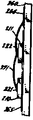
제 11 도는 세라믹 기판위에 설치된 LED와 제 10 도의 2파워 다이리스터 칩을 나타내는 도.FIG. 11 is a diagram showing an LED mounted on a ceramic substrate and a two-power thyristor chip of FIG. 10;
제 12 도는 제 11 도의 측면도. .12 is a side view of FIG. .
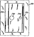
제 13 도는 LED와 파워칩을 둘러싸기 위한 포위캡을 갖춘 제 11 도의 조립을 나타내는 정면도.FIG. 13 is a front view showing the assembly of FIG. 11 with an enclosing cap to surround the LED and the power chip. FIG.
제 14 도는 제 13 도의 상면도.14 is a top view of FIG. 13;
* 도면의 주요부분에 대한 부호의 실명* Real names of symbols on the main parts of the drawings
20 : N(-)층 21,22,23 : P형 영역20: N (-) layer 21, 22, 23: P-type region
24 : N+영역 30 : 산화물층24: N + region 30: oxide layer
31,32 : 폴리실리콘전계판 35 : 이산화실리콘층31,32 polysilicon field board 35 silicon dioxide layer
40 : 캐소드전극 41 : 애노우드전극40: cathode electrode 41: anode electrode
64a,64b,64c,64d : 다이리스터 71 : 제너다이오드64a, 64b, 64c, 64d: Dyistor 71: Zener diode
76,77,78,79 : MOSFET 80 : 기판76,77,78,79: MOSFET 80: substrate
81 : P형 애노우드영역 82 : P형 보조영역81: P type anode area 82: P type auxiliary area
84,90 : 부유가아드링 95 : 스트립84,90: floating guard ring 95: strip
96 : 직사각형96: rectangle
본 발명은 교류고체릴레이 및 고체릴레이에 사용될 수 있는 신규한 다이리스터에 관한 것이다.The present invention relates to a novel thyristors that can be used for alternating solid and solid relays.
고체교류릴레이는 공지되어 있다. 입력과 출력사이에 광학적분리를 한 릴레이들 역시 공지이다. 기존의 장치들에 있어서 많은 분리된 구성요소들은 교류회로를 갖추도록 통상적으로 요구된다. 이에 따라 단일의 장치를 제조하기 위해서는 30개 이상의 분리된 다이리스터, 트랜지스터, 저항기 및 캐패시터를 요한다. 종래부터 전체 고체릴레이의 각종 부품들을 집적하기 위한 시도가 있었으나, 고압 및 고전력 구성요소들 때문에 극히 한정된 성공만을 거두었다. 과거에 만들어진 고체릴레이는 교류전압이 어느정도 작은 "원도우"내에 있을 때만 다이리스터를 턴-온 시키기 위해 제로전압 크로싱 회로를 채용하였다. 또한 이러한 회로는 비교적 복잡해서 주파워 칩내로 집적하기가 어려웠다. 그리하여 제로 크로스 파이어링회로는 파워 단자를 거쳐 접속된 분리 레지스터의 이용을 요구해 왔다. 이들 저항기는 칩표면 위에 이 저항기를 형성하는 것이 어려웠기 때문에 단일칩내에 용이하게 집적되지 않았다. 또한 어떠한 유도성이나 저항성부하하에서 릴레이에 대한 소위 "스너버리스(Snubberless)"작용을 제공하기가 어려웠다. 이에따라 고체릴레이는 저항성이나 약간의 유도성부하하에서는 동작이 잘되는 반면, 높은 유도성부하 하에서는 반사이클동안 릴레이를 턴온시키는 상태인"반파" 또는 "채터(chatter)"로 되는 경향이 있었다. 이것은 종래에 발생했는데 그 이유는 릴레이들이 다소빠른 과도현상이나 높은 dV/dt 상태하에서 회로의 신속한 턴온을 억제시키기 위해 신호조절회로에 제공되었기 때문이다. 그러나 장치가 매우 높은 유도성부하하에서 작동되었을때 전압 과도현상이 장치가 턴온되는 동안에 보통 반복적으로 발생된다. 신호조절(conditioning)회로가 이것을 과도신호로서 잘못 해석했을 때는 동작시 특정의 반이상동안 파워출력을 차단한다. 그 회로는 다음의 반파동안 정상적으로 바뀔것이며 릴레이는 턴온될 것이다. 이 상태는 릴레이가 전파의 하나 혹은 다른 반파사이에만 턴온할 수 있도록 반복된다. 이 상태를 피하기 위하여 종래의 릴레이들은 감소된 파이어링(firing)감도로 형성되었으며 이는 광학적 파이어링 감도의 감소가 요구된다.Solid flow relays are known. Relays with optical separation between the input and output are also known. In existing devices many separate components are typically required to have an alternating current circuit. As a result, more than 30 separate thyristors, transistors, resistors, and capacitors are required to manufacture a single device. Attempts have been made to integrate various components of the entire solid state relay, but with very limited success due to high voltage and high power components. Solid-state relays made in the past employ zero voltage crossing circuits to turn on the thyristor only when it is in a "window" where the AC voltage is somewhat small. These circuits were also relatively complex, making it difficult to integrate into main power chips. Thus, the zero cross firing circuit has demanded the use of a separate resistor connected via a power terminal. These resistors were not easily integrated into a single chip because it was difficult to form these resistors on the chip surface. It was also difficult to provide the so-called "Snubberless" action on the relay at any inductive or resistive load. As a result, solid-state relays tend to operate well under resistive or slightly inductive loads, while at high inductive loads they tend to be "half wave" or "chatter", which turn on the relay for half a cycle. This has occurred conventionally because relays were provided in the signal conditioning circuit to suppress the fast turn-on of the circuit under rather fast transients or high dV / dt conditions. However, when the device is operated at very high inductive loads, voltage transients usually occur repeatedly while the device is turned on. When a conditioning circuit misinterprets this as a transient signal, it shuts down the power output for more than half of its operation during operation. The circuit will change normally during the next half wave and the relay will turn on. This state is repeated so that the relay can turn on only between one or the other half waves of the radio wave. In order to avoid this condition, conventional relays have been formed with reduced firing sensitivity, which requires a reduction in optical firing sensitivity.
종래 릴레이들은 비교적 복잡하기 때문에, 그 하우징에 대해 충분한 체적이 필요하였다. 더우기 과거의 고체릴레이들은 그 전류 취급능력을 한정하는 최대온도상승이 약 100℃까지 한정되었었다. 결국 종래의 고체릴레이는 대단히 많은 분리된 구성요소와 큰 하우징을 필요로 하는 점에서 비교적 고가였다. 단독으로 또는 이와같은 릴레이에 사용될 수 있는 광학적으로 파이어링되는 횡 다이리스터는 역시 공지이다. 그러나 이러한 장치들은 비싸고 비교적 높은 순방향 강하(forward drop)을 가지며 입력방사에 대해 비교적 둔감하다. 이형의 한 다이리스터 WKD치는 예를들면 1982년 10월 19일자 U.S.P. 4,335,320(명칭 : 광제어 트랜지스터)에 기술되어 있다.Since conventional relays are relatively complex, sufficient volume is needed for the housing. Furthermore, the solid state relays of the past have limited the maximum temperature rise to about 100 ° C, which limits their current handling capability. As a result, conventional solid-state relays are relatively expensive in that they require a large number of separate components and large housings. Optically fired transverse thyristors that can be used alone or in such relays are also known. However, these devices are expensive, have a relatively high forward drop, and are relatively insensitive to input radiation. One type of thyristor WKD value is, for example, U.S.P. 19 October 1982. 4,335,320 (name: light control transistor).
본 발명에 따르면, 2개의 동일하고 신규한 다이리스터 파워칩이 교류릴레이용으로 제공되어 있으며 각 파워칩은 각 장치의 한 표면에 양 캐소드 및 애노우도 전극을 갖춘 측면구조로 되어있고 각각의 칩들은 광학적으로 파이어링될 수 있으며 조광되었을때 장치가 그의 애노우드와 캐소도 전극사이에 전도성이 되도록 광학적으로 민감한 상부표면을 갖는다. 각각의 다이리스터의 게이트회로는 신규한 제어회로에 접속되어 있으며 분리된 구성요소들중의 하나 또는 다이리스터를 형성하는 반도체재료의 본체내에 채용된 구성요소들중 하나를 형성한다. 제어회로는 장치에 걸린 전압이 어떤 소정의 윈도우 값보다 더 큰 값으로 초과했을 때 또는 높은 dV/dt 과도현상이 장치에 나타냈을때 비록 표면이 조광되었더라도 턴온을 방지하기 의해 작동될 수있다. 이 제어회로는 그 각각의 다이리스터의 게이트를 클램프하도록 턴온될 수 있는 클램프 트랜지스터와 주파워 전극을 가로질러 연결된 용량성분할회로를 포함한다. 용량성분할기는 제어트랜지스터에 제어신호를 가한다. 용량성 분할기의 캐패시터중 하나는 제어트랜지스터의 분배된 용량을 포함한다. 제어트랜지스터가 ON상태인 한, 그의 각각의 파워 다이리스터는 비록 그의 표면이 조광되었더라도 턴온될 수 없다. 용량성 분할기는 제어트랜지스터가 어떤 비교적 작은 원도우치 보다 큰 주장치에 걸린 모든 절대전압에 대해 통상적으로 턴온될 수 있도록 배치된다. 이에 따라 파워 다이리스터는 이 작은 윈도우 값이나 제로크로스 값의 의측을 턴온할 수 없다. 제어트랜지스터와 결합되어 있는 신규한 용량성 분할기는 두 빠른 과도현상을 억제하기 의해 작용하며 또한 그 장치가 정상적인 부하상태하에서 작용할 수 있게한다. 이에 따라 장치가 높은 유도성 부하 상태하에서 턴온되는 동안에 반복적으로 발생되는 전압과도현상이 빠른 과도현상으로 잘못 해석되지 않을 것이며 파워 다이리스터칩은 높은 유도성부하하에서 정상상태로 턴온할 수 있다.According to the present invention, two identical new thyristor power chips are provided for the AC relay, each power chip having a side structure with both cathode and anode electrodes on one surface of each device and each chip. They can be optically fired and have an optically sensitive top surface so that when illuminated the device is conductive between its anode and the cathode electrode. The gate circuit of each thyristors is connected to a novel control circuit and forms one of the discrete components or one of the components employed in the body of semiconductor material forming the thyristors. The control circuit can be operated by preventing the turn-on even if the surface is illuminated when the voltage across the device exceeds a certain window value or when a high dV / dt transient is present in the device. This control circuit includes a clamp transistor that can be turned on to clamp the gate of each respective thyristor and a capacitive component circuit connected across the main power electrode. The capacitive component separator applies a control signal to the control transistor. One of the capacitors of the capacitive divider includes the distributed capacity of the control transistor. As long as the control transistor is ON, each of its power thyristors cannot be turned on even if its surface is illuminated. The capacitive divider is arranged such that the control transistor can typically be turned on for all absolute voltages present in the main unit larger than any relatively small window. As a result, the power thyristor cannot turn on the side of this small window value or zero cross value. The novel capacitive divider, combined with the control transistor, works by suppressing two fast transients and also allows the device to operate under normal load. This ensures that voltage transients that occur repeatedly while the device is turned on under high inductive loads will not be misinterpreted as fast transients and that the power thyristor chip can turn on at high inductive loads.
본 발명의 신규한 신호조절기(signal conditioner)는 오파이어링없이 본 장치의 광학적 감도의 개량을 기대할 수 있다. 시중에서 입수할 수 있는 광학적으로 분리된 드라이액 드라이버와 그와 유사한 것들은 과도현상으로 부터 저 레벨명령 신호를 분리하기 위한 그들의 무능력때문에 dV/dt 능력이나 광학적 감도에 있어 항상 제한되었다. 신규한 하우징은 2개의 칩 배치가 제공되며 상기 2칩은 다른 하나와 병렬로 용이하고 저렴하게 접속되고 외부 환경으로 부터 보호된다. 알루미늄 기판 또는 다른 적절한 열적으로 도전성이나 전기적으로는 절연성인 기판은 스위치의 여러칩을 내장하고 적절한 출력 리이드에 칩전극을 접속하기 위해 기판위에 적합한 도전성 패턴이 제공된다. 서로 역평행으로 접속될 2개의 동일한 다이리스터 칩들은 기판위의 각각의 도전성 패드에 대칭적으로 고정되어 있으며 다른 하나와 그리고 기판위의 두도전성 패턴의 끝과 일직선으로 되어있다.The novel signal conditioner of the present invention can be expected to improve the optical sensitivity of the device without opposing. Commercially available optically isolated dry liquid drivers and the like have always been limited in their dV / dt capability or optical sensitivity because of their inability to separate low level command signals from transients. The novel housing is provided with two chip arrangements, which are easily and inexpensively connected in parallel with the other and protected from the external environment. Aluminum substrates or other suitable thermally conductive or electrically insulating substrates are provided with suitable conductive patterns on the substrate to embed several chips of the switch and connect the chip electrodes to the appropriate output leads. Two identical thyristor chips to be connected antiparallel to each other are symmetrically fixed to each conductive pad on the substrate and are in line with the other and the end of the two conductive patterns on the substrate.
두 연속적 와이어는 다이리스터 패드 및 리이도 와이어가 한칩의 애노우드패드, 제2칩의 캐소드패도 및 입력교류리이드에 접속된 도전성 패턴중 하나에 전기적으로 접속되는 상태로 도전성 리이드들에 스티치본드(stitch-bonded)된다. 다른 와이어는 서로 역평행으로 다이리스터들을 접속하기 위해 도전성 패턴 및 다른 전극들에 유사하게 된다. 작은 LED칩은 파워칩이 연결됨과 동시에 알루미나기판에 연결된다. LED는 교류출력리이드로 부터 확실하게 절연된 두 입력리이드에 적절하게 접속된다.The two consecutive wires are stitch bonded to the conductive leads with the diester pad and the lid wire electrically connected to one of the anode pads of one chip, the cathode pad of the second chip, and the conductive patterns connected to the input alternating leads. -bonded). The other wire becomes similar to the conductive pattern and the other electrodes to connect the thyristors antiparallel to each other. The small LED chip is connected to the alumina substrate at the same time that the power chip is connected. The LEDs are properly connected to two input leads that are reliably isolated from the AC output leads.
다음 흰 조광반사재료로 덮여진 플라스틱 캡이 기판에 고정되고 LED를 포함하는 기판의 영역 및 두파워칩 덮는다. 캡은 칩의 표면을 싸거나 포위한 투명한 실리콘 및 흰실리콘으로 페인트된 외측표면을 갖춘 그의 내부 결선리이드들로 구성될 수 있다. 만일 파워 트랜지스터에 대한 제어회로가 분리된 형태로 수행된다면, 그 분리된 구성요소들은 이 기판에 적절하게 접속될 수 있다. 그러나, 바람직하게는 이들 구성요소들은 전고체 릴레이가 두 파워칩 및 그들의 제어장치들, LED칩 및 상기한 각종 지지구조물로 구성되도록 하기 위하여 개별적인 파워칩내에 집적된다.A plastic cap covered with a white dimming reflective material is then secured to the substrate and covers the area of the substrate containing the LEDs and the two power chips. The cap may consist of its inner connection leads with an outer surface painted with transparent silicon and white silicon surrounding or enclosing the surface of the chip. If the control circuit for the power transistor is performed in a separate form, the separate components can be properly connected to this substrate. Preferably, however, these components are integrated in separate power chips so that the all-solid-state relay consists of two power chips and their control devices, LED chips and the various supporting structures described above.
릴레이의 각각의 다이리스터는 신규한 구조로서 낮은 순방향 전압강하 및 비교적 높은 전류용량을 갖는 단일칩에 형성되며 논크리티칼 LED 트리거링 소오스는 다이리스터를 통전시키기 위해 제공될 수 있도록 입력방사에 대해 고도로 민감하다. 평행으로 접속된 제어 MOSFET, 저항기, 제어다이오드 및 캐패시터를 포함하는 릴레이 회로 제어 구성요소는 단일칩내에 구비될 수 있다. 릴레이 제어구성요소는 애노우도 대 캐소드전압이 소정치보다 적을 때만 다이리스터를 턴온 하도록 한다. 더욱이, LED가 오프되면, 과도전류로 인한 잘못된 턴온은 모든 전류 조건하에서 방지된다.Each diester of the relay is a novel structure, formed on a single chip with low forward voltage drop and relatively high current capability, and the non-critical LED triggering source is highly sensitive to input radiation so that it can be provided to energize the diester. Do. Relay circuit control components, including control MOSFETs, resistors, control diodes, and capacitors connected in parallel, may be provided in a single chip. The relay control component turns on the thyristors only when the anode-to-cathode voltage is below a predetermined value. Moreover, when the LED is off, false turn-on due to transients is prevented under all current conditions.
본 발명에 따르면, 각각 광학적으로 파이어링될 수 있는 다수의 개별적 횡 다이리스터가 단일칩내에 다른것과 병렬로 접속되어 있다. 각각의 횡 다이리스터는 베이스내에 형성된 에미터 소자를 갖춘 각각의 베이스를 갖는다. 각 베이스의 두측면과 끝을 포장하는 다수의 간격을 둔 애노우도 영역 핑거(finger)로 구성되는 신규한 애노우도 영역은 소자의 평행 접속을 용이하게 해준다. 다이리스터 베이스영역은 거리를 둔 평행에미터 영역을 포함하며, 그 베이스영역은 보조 P영역에 의해 둘러싸여진다. 측면의 광학적으로 트리거되는 다이리스터에 대한 보조영역은 USP 4,355,320에 나타나있다. 그러나 본 발명의 신규한 보조영역은 둥글게 형성되어 개별적 베이스영역을 전부 둘러싸며 금속 캐소드 전극에 단단하게 접속된 도전성 폴리실리콘 전계판에 저항성 접속을 한다. 신규한 저항성 접속은 전계판으로부터 보조영역 까지 거리를 두어 접속함으로써 얻어질 수 있다. 이러한 식으로 저항성 접속을 사용함으로써 애노우도 영역으로부터 주입되어 에미터로 향하여 측면으로 이동하는 보다 많은 캐리어가 에미터에 도달할 것이다. 이것은 장치의 동작동안에 전력손실을 현저하게 감소시키는 중요한 양(예를들면,1.45V 내지 1.15V)만큼 장치의 순반향 전압강하를 개량한다.According to the invention, a number of individual transverse thyristors, each of which can be optically fired, are connected in parallel with the other in a single chip. Each transverse thyristor has a respective base with emitter elements formed in the base. The novel anode region, which consists of multiple spaced anode region fingers wrapping the two sides and ends of each base, facilitates parallel connection of the devices. The thyristor base region includes a distanced parallel emitter region, which base region is surrounded by the auxiliary P region. Auxiliary areas for laterally optically triggered thyristors are shown in US Pat. No. 4,355,320. However, the novel auxiliary region of the present invention is rounded and resistively connects to a conductive polysilicon field plate that surrounds all of the individual base regions and is tightly connected to the metal cathode electrode. The novel resistive connection can be obtained by connecting at a distance from the field plate to the auxiliary region. By using a resistive connection in this way, more carriers will arrive at the emitter that are injected from the anode region and laterally moved towards the emitter. This improves the forward voltage drop of the device by an important amount (e.g., 1.45 V to 1.15 V) which significantly reduces power loss during operation of the device.
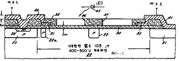
본 발명의 또 다른 특징에 따르면 애노우도 영역은 순방향 강하를 다시 감소시키는 에미터 도우핑에 비교하여 비교적 고밀도로 도우프될수도 있다. 에미터 영역표면의 에미터 도우핑농도는 주입능를을 향상하기위해 최적인 되는 정도로 제어된다. 특히 에미터 표면에 l×102°내지 6×10²°인 이온/cc의 표면농도를 사용할때 매우 양호한 동작이 얻어진다. 결국 장치에 대한 표면접점을 만들 때 비교적 두꺼운 알루미늄의 얇은 라인들은 실리콘의 최대량을 표시하도록 사용된다. 이하, 본 발명을 첨부도면을 참조하여 상세히 설명한다. 제 1 도는 본 발명에 따라 제조되는 횡 다이리스터 칩을 금속화할 때 접합패턴의 단면도를 보인 것이다. 제 1 도의 횡 다이리스터를 포함하는 칩은 어떠한 소망의 사이즈 및 외형을 가질 수 있으며, 그것은 단결정실리콘의 칩이다.According to another feature of the invention the anode region may be doped at a relatively high density compared to emitter doping which again reduces the forward drop. The emitter doping concentration on the emitter area surface is controlled to an optimal level to improve implantation capability. Particularly good behavior is obtained when using surface concentrations of ions / cc of l × 10 2 ° to 6 × 10 2 ° on the emitter surface. As a result, when making surface contacts for the device, thin lines of relatively thick aluminum are used to indicate the maximum amount of silicon. Hereinafter, the present invention will be described in detail with reference to the accompanying drawings. 1 shows a cross-sectional view of a bonding pattern when metallizing a transverse thyristor chip made in accordance with the present invention. A chip comprising the transverse thyristor of FIG. 1 can have any desired size and shape, which is a chip of single crystal silicon.
제 1 도에 나타낸 각종 접합은 N(-)층(20)에 형성된다. 층(20)은 약 20Ω-cm의 저항을 가질 수 있다. 간격을 둔 P형 영역(21,22,23)은 어느 소망의 공정에 의해 칩(20)의 상부표면에 형성된다. 불활동성인 다른 P형영역(23a)은 영역(23)의 주위를 포위할 수 있다. 영역(21,22,23 및 23a)은 P영역의 판저항이 칩표면에 약 1600Ω/cm2이 되도록 하기 위하여 충분한 농도의 붕소확산영역으로 될 수 있다. 그들은 예를들면 그것이 비교적 얕게 도우프될 수 있도록 하기 의하여 cm2당 5×10+l3붕소원자를 채용하여 드라이브-확산공정 및 이온주입에 의해 형성될 수도 있다. 영역(2l)은 다른 P영역들보다 더욱 고밀도로 도우프되는 것이 바람직하다. 영역(21,22,23 및 23a)들은 모두 대략 4μ의 깊이를 가질 수 있다. P형 영역(23)은 횡 다이리스터의 옆으로 거리를 둔 접합부들을 완전하게 하기위해 N(+) 영역(24)을 포함한다.Various junctions shown in FIG. 1 are formed in the N (−) layer 20. Layer 20 may have a resistance of about 20Ω-cm. The spaced P-type regions 21, 22 and 23 are formed on the upper surface of the chip 20 by any desired process. Another inactive P-
영역(21,23)의 대향 에지들은 선택된 전압을 차단할 수 있는 한 가능한한 서로 근접하게 해야한다. 본 출원에서 장치는 약 400 내지 500V를 차단하며, 떨어진 거리는 105μ이다. 영역(21)은 애노우도 영역이며, 영역(23)은 게이트 또는 베이스 영역이며 영역(24)은 에미터 또는 캐소도 영역인 반면에 N(-) 본체(20)는 제 1 도에 도시된 다이리스터의 주 블록킹 영역이다. 영역(22)은 공지형태의 부유가이드 영역으로 칩의 표면에 절연파괴의 위험이 없이 400 내지 500V의 고압을 접합부(21,23) 사이에 차단전압을 증대하도록 한다.Opposite edges of regions 21 and 23 should be as close as possible to each other as long as possible to block the selected voltage. In the present application, the device blocks about 400 to 500 V, with a distance of 105 μ. Region 21 is an anode region, region 23 is a gate or base region and
상부칩 표면은 예컨대 약 1μ의 두께를 갖는 박막 이산화실리콘층(30)으로 덮여진다. 폴리실리콘전계판(31,32)은 종래의 폴리실리콘 부착 및 마스킹기술을 사용하여 도시된 바와같이 산화물층(30)위에 형성된다. 폴리실리콘 전계판을 포함, 칩의 전상부표면과 산화물층(30)은 종래의 유리질 및 인으로 도우프된 이산화실리콘층(35)로 덮여진다. 공지구조의 간격을 둔 갭(36,37)은 인으로 도우프된 산화물층(35)내에 측면의 분극작용이 부유가아드영역(22)에 인접한 영역(20)의 표면에서의 전계분포를 방해하지 못하도록 부유가아드영역(22)의 각 단에 위치될 수 있다.The upper chip surface is covered with a thin film silicon dioxide layer 30 having, for example, a thickness of about 1 mu. Polysilicon field plates 31 and 32 are formed on the oxide layer 30 as shown using conventional polysilicon deposition and masking techniques. The top surface of the chip and the oxide layer 30, including the polysilicon field plate, are covered with a conventional silicon dioxide layer 35 doped with glassy and phosphorous. The spaced gaps 36 and 37 of known structures prevent the electric field distribution at the surface of the region 20 adjacent to the floating guard region 22 due to the polarization of the side in the oxide layer 35 doped with phosphorus. It may be located at each end of the floating guard region 22 so as not to.
상기 에미터영역(24) 및 애노우드영역(21)이 여러영역 및 전계판에 접촉할 수 있도록 하기 위해 적절한 개구들이 산화물층(30,35)에 형성된다. 이에따라 알루미늄 캐소드전극(40) 및 애노우드전극(41)은 도시된 바와같이 에미터영역(24) 및 애노우드영역(21)에 각각 결합된다. 산화물층(35)에 형성된 다른 개구들은 캐소드(40)에서 전계판(31)에 그리고 애노우드(41)에서 전계판(32)까지 연결할 수 있게한다. 양 캐소드전극(40) 및 애노우드전극(41)은 비교적 얇으며 예컨데 대략 4μ의 두께로 할 수있다. 영역(23a)은 캐소드(40)에 바람직하게 저항식으로 연결된다. 이에따라 영역(23a)은 그들의 주위에 따라 간격을 둔 점들에만 캐소드(40)에 연결될 수 있다. 제 1 도의 횡적인 다이리스터는 에미터영역(24)으로 부터 게이트영역(23)내로 캐리어의 주입에 의해 턴온된다. 적절한 주입은 본체(20)에 있어 캐리어. (정공)을 발생할 장치의 상부표면에 방사를 가함에 의해 얻어질 수 있다. 이들 호올들은 영역(23)으로 이동하여 장치를 턴온시키기 위해 베이스드라이브로서 작동하도록 영역(23,24) 사이의 에미터접합에 의해 콜렉트된다. 적절한 방사원은 장치의 표면을 조광하도록 배치된 개략적으로 나타낸 LED(45)일 수 있다. 제 1 도의 구조를 채용한 장치는 400 내지 500V를 차단할 수 있다. 순방향 도전동안에 순방향 전압강하는 대략 1.5 암페어 순방향 전류에서 약 1.15볼트있다.Appropriate openings are formed in the oxide layers 30 and 35 to allow the
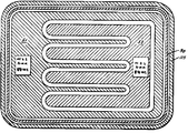
제 1 도의 횡방향 다이리스터의 배치는 바람직한 기하학적 측면에 있어 소정의 수로 충족될 수 있다. 특히 효과있는 기하학은 현재 기술되고 있는 제 2 도 내지 제 9 도에 나타낸 것이며 제 1 도의 그것과 같이 다수의 장치가 병렬로 접속되어 있는 배치를 보여준다. 제 2 도 및 3도를 참조하면, 단일의 다이리스터 장치와 그의 제어회로 구성요소들을 포함하는 단일의 칩의 평면도를 나타낸다. 제 2 도와 3도의 칩은 통상의 공정이 완료된 후 분리되어 있는 보통 웨이퍼위의 많은 칩들중의 하나이다. 그 칩은 제 2 도에 나타냈으며 캐소드와 애노우도 단자 전극의 금속화후이다. 칩표면의 접합패턴은 제 3 도에 나타냈다. 다수의 분리된 다이리스터 소자들은 꾸불꾸불하거나 손을 마주낀 모양의 통로로 이후에 표시된 통로를 따라 연장되어 있는 애노우드,베이스 및 에미터영역에 대한 신규한 패턴(제 3 도 및 제 4 도)을 사용하여 평행으로 연결되어 있으며, 이에 의해 그들은 가능한한 가장 긴 길이를 지니게되어 장치가 높은 전류용량을 갖도록 하는 것이다. 제 2 도 및 제 3 도의 실시예에 있어서, 칩은 82mm의 폭과 113mm의 길이를 가지며,1.15V의 순방향 전압강하로 1.5A의 순방향 전류이동률을 갖는다. 장치의 양대칭차단능력은 대략 피이크 500V이다. 따라서, 본 발명의 다이리스터칩은 역평행 접속된 동일한 다이리스터 칩과 함께 채용될 수 있으며 280V까지의 실효전압을 갖는 교류회로를 제어하기 위한 고체 릴레이에 사용된다. 제 2 도의 기본 금속화 패턴은 도시된 바와 같은 형상의 캐소드(50)와 애노우드(51)를 채용한다. 제 2 도에는 도시되지 않았으나, 제어회로는 칩본체내에 내장된다. 회로는 제 9 도에 나타난다. 제 3 도의 금속화영역(60,61)은 제 9 도에 나타낸 2개의 캐패시터의 전극들이다.The arrangement of the transverse thyristors of FIG. 1 can be met in any number of preferred geometric aspects. Particularly effective geometries are shown in FIGS. 2-9 which are now described and show an arrangement in which a number of devices are connected in parallel, as in FIG. 2 and 3, a plan view of a single chip including a single thyristor device and its control circuit components is shown. The second and third degree chips are one of many chips on a normal wafer that are separated after the normal process is completed. The chip is shown in FIG. 2 and after metallization of the cathode and anode terminal electrodes. The bonding pattern of the chip surface is shown in FIG. A number of separate thyristors are novel patterns for the anode, base, and emitter regions that extend along the passages shown later, as serpentine or hand-shaped passages (FIGS. 3 and 4). Are connected in parallel, whereby they have the longest possible length so that the device has a high current capacity. In the embodiments of FIGS. 2 and 3, the chip has a width of 82 mm and a length of 113 mm and a forward current transfer rate of 1.5 A with a forward voltage drop of 1.15 V. FIG. The device's bisymmetrical blocking capability is approximately 500 V peak. Therefore, the thyristor chip of the present invention can be employed together with the anti-parallel connected same thyristor chip and is used in a solid state relay for controlling an AC circuit having an effective voltage of up to 280V. The basic metallization pattern of FIG. 2 employs a cathode 50 and an anode 51 in the shape as shown. Although not shown in FIG. 2, the control circuit is embedded in the chip body. The circuit is shown in FIG. The metallization regions 60 and 61 of FIG. 3 are the electrodes of the two capacitors shown in FIG.
캐패시터(60)는 제 7 도를 참조하여 뒤에 기술될 것이다. 전극(60,61)을 포함하는 캐패시터는 제 9 도에 도시한 바와같이 평행으로 접속되며, 다이리스터(64a,64b,64c및 64d)의 애노우드와 제어 MOSFET(76,77,78 및 79)의 게이트 사이에 각각 연결되어 있다. 다이리스터들(64a,64b,64c,64d)은 평행으로 있으며 제 2 도 및 제 6 도에 있어서 캐소드(50) 및 애노우드(51)로서 나타낸 공통 캐소드 및 애노우드를 갖는다. 폴리실리콘으로 형성되고 캐소드와 각각의 다이리스터(64a,64b,64c,64d)의 제이트 사이에 전기적으로 접속된 100KΩ 저항기(70)가 제 3 도의 칩으로 짐적되어 구비된다. 저항기(70)의 상세한 구성은 제 8 도와 관련하여 뒤에 기술될 것이다. 부가적으로 제 9 도에 나타낸 바와같이 제너다이오드(71)가 제 3 도의 칩에 일체적으로 형성되어 있으며 애노우드와 도시된 다이리스터의 캐소드단자(50,51) 사이에 캐패시터(60,61)와 직렬로 접속되어 있다. 또한 제9에는 제너다이오드(71)와 병렬로 고유분포 캐패시터(75)가 도시되어 있다. 제너다이오드(71)는 불활성 P영역(82)에 형성될 수 있으며 제 3 도에 나타낸 N+영역(71a)으로 구성될 수 있다. 한제너단자(71b)는 N+영역(71a)의 상부에 직접 형성될 수 있으며, 다른단자는 캐소드전극에 접속된 금속접점(71c)으로 형성될 수 있다. 제 3 도 및 제 4 도로 위에 기술될, 제 9 도에 나타낸 다수의 제어 MOSFET(76,77,78,79)들은 칩위에 내장되어 있으며 다이리스터(64a,64b,64c 및 64d)로 각각 작동한다. 각각의 제어 MOSFET는 작동지연시간이 제한되고 회로대칭이 보장될 수 있도록 그의 각각의 주다이리스터부재에 밀접하여 배치되어 있다.Capacitor 60 will be described later with reference to FIG. Capacitors comprising electrodes 60, 61 are connected in parallel as shown in FIG. 9, and the anodes of the thyristors 64a, 64b, 64c and 64d and the
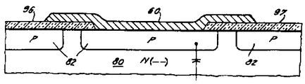
이제 제 2 도 내지 제 8 도에 관련되어 기술될 제 9 도의 회로는 신규한 방법으로 수행된다. 여기에 기술된 실시예는 4개의 병렬 다이리스터(64a,64b,64c,64d)를 사용하며 소정수의 어느 소자도 사용될 수 없다. 제 3 도 내지 6 도를 참조하면, 전체의 집적된 장치는 약 20Ω-cm의 저항성을 가질 수 있는 비교적 높은 저항N(-)기판(80)에 형성된다. 많은 개별적인 P형 영역들은 어떤 소망의 공정에 의해 기판(80)에 형성된다. 이들의 첫번째는 제 1 도의 애노우드영역(21)에 대응하는 P+형 애노우드영역(81)이다. 제 3 도 및 제 4 도에 나타낸 바와같이, 애노우도 영역(81)은 3개의 평행 핑거(finger)(81a,81b,81c)가 뻗어있는 주본체부를 갖는다. 81a 및 81b는제 4 도 및 6도에 더욱 상세히 나타냈다. 레그(81a,81e 및 81f)들을 갖는 직사각형 애노우드영역 프레임 은 제 3 도에 나타낸 바와같이 칩의 주위를 둘러싼다. 레그(81d,81e)는 제 5 도에 나타냈다.The circuit of FIG. 9, which will now be described in connection with FIGS. 2-8, is performed in a novel way. The embodiment described here uses four parallel thyristors 64a, 64b, 64c, 64d and no number of elements can be used. 3-6, the entire integrated device is formed on a relatively high resistive N (−)
제 3 도 내지 8 도에 나타낸 제2 P형 영역은 "불활성" P형 보조영역(82)이다. 불활성영역(82)은 루우프부(82a,82b,82c 및 82d)(제 3 도)를 가지며, 뒤에 기술될 4개의 각각의 다이리스터의 베이스를 포위하여 제 1 도의 보조링(23a)이 목적을 수행한다. 루우프부(82b)는 제 6 도에 나타냈다. 4개의 동거리로 떨어진 길게 연장된 P형 베이스영역(83a,83b,83c,83d)(제 3 도,4도 및 6도)들은 영역 80에 형성되어 있다. 이를 베이스영역들은 제 1 도의 베이스영역(23)에 대응한다. 베이스영역(83b)은 제 4 도에 확대하여 상세히 나타낸다. 베이스영역(83a,83b,83c 및 83d)은 보조링루우프(82a,82b,82c 및 82d)에 의해 거의 전부 포위되어 있는 것을 주목해야 한다.The second P-type region shown in FIGS. 3-8 is an "inactive" P-type
부유 가아드링(84)로 구성되는 또다른 P형 영역이 형성되어 있는데, 이는 제 3 도 내지 6도에 나타냈다. 가아드링(84)은 물결모양의 경로로 연장되어 있으며 제 3 도와 제 4 도의 장치표면에 도달하는 N(-)영역(80)을 절반으로 분할한다.Another P-type region consisting of floating
각각의 다이리스터 베이스(83a,83b,83c 및 83d)은 2개의 평행한 N+에미터 영역(85a-85b,86a-86b,87a-87b 및 88a-88b)를 각각 내장한다(제 3 , 4 및 6도).Each of the thyristor bases 83a, 83b, 83c and 83d contains two parallel N + emitter regions 85a-85b, 86a-86b, 87a-87b and 88a-88b, respectively (third, fourth, and fourth). And 6 degrees).
에미터 영역(86a,86b)은 제 4 도에 확대하여 상세히 나타냈다. 상기로 부터 제 3 도의 접합패턴은 제 9 도의 4개의 다이리스터소자(84a,84b,84c 및 84d)에 대한 근간을 형성하며 장치의 평행접속을 가능하계 한다는 것을 알 수 있을 것이다. 다이리스터(64b)를 한정하는 다이리스터 소자는 제 4 도 및 6도에 나타냈으며 이제부터 기술된다. 다이리스터 베이스는 팽행에미터 영역(86a,86b)을 포함하는 활동성 P영역(83b)으로 이루어진다. 다이리스터 애노우도 영역은 베이스(83b)를 대칭적으로 둘러싸는 애노우도 영역 핑거(8la 및 81b)로 구성된다. 다이리스터 본체는 N(-)영역 (80)으로 이루어진다. 또한 베이스는 집적능력을 증대하는 상기 이점을 지닌 보조 루우프 영역(82b)에 의해 거의 완전하게 둘러싸인다. 역시 신규한 접합패턴은 칩위에 다수의 다이리스터의 병렬접속을 가능하게 한다. 도시된 접합패턴은 형성함에 있어, 베이스 영역(83a,83b,83c 및 83d)과 각각의 인접 애노우도 핑거(81a,81b, 및 81c)(및 외축 애노우드 레그,81d 및 81e) 사이의 측면거리는 약 105미트론이다. P형 영역들의 각각의 깊이는 약 4미크론이다. 각각의 베이스 영역(83a,83b,83c 및 83d)는 약 40밀리의 길이 및 약 75미크론의 폭을 갖는다. 여러 P영역들을 형성하는 동안에 다른 P형 가아드링(90)(제 2 도 및 5도)은 칩의 주변둘레에 바람직하게 형성된다. 링(90)은 약 38미크론 만큼 P+애노우드(81e)의 외주로 부터 떨어져 있다. 또한 제 3 도 및 제 4 도에 나타낸 바와 같이 여러 접합들을 형성하는 동안에 N(+)소오스 및 드레인 영역(91a-91b,92a-92b,93a-93b 및 94a-94b)들은 제 9 도에 있어서 제어MOSFET(76,77,78,79)용으로 각각 형성된다. 이들은 확대불활성 P형 영역(82)에 형성된다.Emitter regions 86a and 86b are shown in greater detail in FIG. It can be seen from the above that the junction pattern of FIG. 3 forms the basis for the four thyristor elements 84a, 84b, 84c and 84d of FIG. 9 and is capable of parallel connection of the devices. The thyristor element defining the thyristor 64b is shown in FIGS. 4 and 6 and will now be described. The thyristor base is made up of an active P region 83b including bulging emitter regions 86a and 86b. The thyristor anode region is composed of anode region fingers 8la and 81b symmetrically surrounding the base 83b. The thyristor body consists of an N (-)
제어 MOSFET(77)의 경우에 대해 제 4 도에 나타낸 바와 같이, 약 0.1미크론의 두께를 갖는 적절한 게이트 산화물 및 폴리실리콘 게이트전극(도시되지 않음)은 영역 92a 및 92b 사이의 갭위에 배치된다.As shown in FIG. 4 for the case of
국도로 얇은 산화물은 게이트가 캐패시터(60 및 61) 및 캐패시터(75)사이의 노우드의 전위에 있기 때문에 제어 MOSFET용으로 사용될 수 있다.Locally thin oxides can be used for control MOSFETs because the gate is at the potential of the nod between capacitors 60 and 61 and capacitor 75.
이에따라 제어 MOSFET 게이트들과 주 다이리스터들의 캐소드 사이의 전위차는 매우 낮다. 따라서 트랜지스터(76 내지 79)는 매우 높은 이득의 트랜지스터로 될수 있다.Accordingly, the potential difference between the control MOSFET gates and the cathode of the main thyristors is very low. Thus, the transistors 76 to 79 can be very high gain transistors.
소오스영역(92a)는 불활성 베이스에 연결되고, 반면에 드레인 영역(92b)은 도전성스트립(95)(제 4 도 및 6도)을 통하여 다이리스터 베이스영역(83b)에 전기적으로 접속되어 있다. 스트립(95)은 금속이 바람직하다.The source region 92a is connected to the inert base, while the drain region 92b is electrically connected to the thyristor base region 83b via the conductive strip 95 (FIGS. 4 and 6). Strip 95 is preferably metal.
베이스(83a,83b,83c,83d)를 연결하는 도전성 스트립을 갖춘 각 다이리스터소자가 제어 MOSFET 소오스전극(91a,92b,93c,94d)를 각각 제어하도록 상기와 비슷한 배치가 제공된다. 다음 도전성 스트립은 점선(95a)으로 제 4 도에 부분개략적으로 나타낸 폴리실리콘 연결스트립에 의해 모두 함께 접속되어 있다.Similar arrangements are provided such that each thyristor element with conductive strips connecting the bases 83a, 83b, 83c, 83d controls the control MOSFET source electrodes 91a, 92b, 93c, 94d, respectively. The conductive strips are then all connected together by polysilicon connecting strips, shown schematically in FIG. 4 by dashed lines 95a.
또한 캐패시터(60,61)는 캐패시터(60)에 대해 제 7 도에 나타낸 바와 같이 불활성 P영역(82)에 설치되어있다. 이에 따라 캐패시터(60)는 직사각형 링(96)에 적절한 반경방향의 코오너를 갖도록 함에 의해 칩으로 부터 분리된 P형 베이스(82) 및 침표면에 도달하도록 N(-) 재료(80)의 영역위에 금속층을 퇴적함으로써 형성된다.Capacitors 60 and 61 are provided in the
금속층(60)은 전계판을 형성하기 위해 열산화물층(97)위에 있는 것을 주목해야 한다.Note that the metal layer 60 is over the
또한 저항기(70)는 제 8 도에 나타낸 바와같이 불활성 P형 영역(82)에 설치되어 있다. 이에따라, 제 8 도에서 폴리실리콘 스트립(70a)은 산화물층(97)위에 부착되고, 부착된 이산화 실리콘층(98)과 함께 뒤덮여진다. 따라서 저항기(70)은 절연층(97)에 의해 칩분체로 부터 완전히 절연된 저항층으로 형성된다.In addition, the
이에따라 저항기(70)는 다른 회로구성요소들과의 기생 간섭이 없는 이상적인 저항기로 된다.The
다음 개구들은 층(98)에 형성되어 있으며 저항기 단자접속(99,100)은 저항기로 만들어진다. 이들 단자들은 다이리스터 캐소드 및 제어 MOSFET(76,77,78,79)의 소오스전극에 적절히 접속되어 있다.The following openings are formed in layer 98 and
제 5 도 및 6 도에 나타낸 칩의 상면은 소정의 금속화를 하도록 처리된다. 금속화되기전에 적당한 열적산화물(110)이 제자리에 존재하거나 개략 1미크론의 두께로 장치표면에 가해진다. 종래의 마스킹 및 에칭단계 후 금속들은 필요한 순서로 가해진다. 다음 상면은 어떤 소정두께를 가질수 있는 부착된 산화물 코팅으로 덮여진다.The upper surface of the chip shown in FIGS. 5 and 6 is processed to give a predetermined metallization. Before metallization, a suitable thermal oxide 110 is present in place or applied to the device surface to a thickness of approximately 1 micron. After conventional masking and etching steps the metals are applied in the required order. The top surface is then covered with an attached oxide coating that can have any desired thickness.
신규한 폴리실리콘 전계플레이트(112,113)는 열적산화물(110)위에 부착된다. 모든 폴리실리콘 스트립이나 층들은 어떤 소정순서로 부착될 수 있음을 유의해야 한다. 전계판(112)은 상부에 배치된 기다랗고 꾸불꾸불한 판이며 P(+) 애노우도 영역(81)과 N(-)영역(80) 사이의 접합의 경로를 흐른다. 비슷하게 전계판(113)은 플레이트(1l2)의 그것과 평행의 경로를 잇는 기다랗고 꾸불꾸불한 판이며 보조 영역(82)과 외측으로 배치된 N(-)영역 (80)사이의 접합위에 실시된다.The novel polysilicon field plates 112 and 113 are deposited on the thermal oxide 110. It should be noted that all polysilicon strips or layers may be attached in any order. The electric field plate 112 is an elongated and serpentine plate disposed on the upper portion, and flows through the junction path between the P (+)-
전계플레이트(112) 및 (113)이 부착될 때 외부등 위링(115)(제 5 도)도 칩의 외주주위에 배치될 수있다. 링(115)은 보통 방식으로 기판(80)에 연결된다.When the electric field plates 112 and 113 are attached, the outer light ring 115 (FIG. 5) can also be arranged around the outer periphery of the chip.
전계플레이트(112),(113)와 링(115)은 각각 약 20미크론의 폭을 갖는다. 보호링 영역(84)은 약 8미크론의 폭을 갖고 있고 플레이트(112)와 (113)의 서로 마주보는 변 사이의 중간에 배치되는 데 이 마주보는 두변 사이의 거리는 약 44미크론이다. 이와 마찬가지로 P형 영역(90)(제 5 도)은 두변이 서로 44미크론 격치되어 있는 플레이트(112)와 플레이트(115)사이의 중간에 위치되어 있다.Field plates 112, 113 and
그 다음 양극(51)을 도시한 바와같이 형성되여 제 2 도 및 제 6 도에 나타낸 바와같이 P형 양극 (81)에 연결시킨다. 또한 제 2 도, 제 5 도 및 제 6 도에 표시한 바와같이 음극(50)을 형성한다.An anode 51 is then formed as shown and connected to the P-
제 2 도 내지 제 9 도의 횡 다이리스터는, 칩의 노출면을 조명하도록 배치된 LED(45)(제 6 도 및 제 9 도)로부터의 복사에 의해 도통된다.The transverse thyristors of FIGS. 2-9 are conducted by radiation from LEDs 45 (FIGS. 6 and 9) arranged to illuminate the exposed surface of the chip.
칩은 극히 예민하기 때문에 LED(45)는 크기, 출력 또는 위치가 특히 중요하지는 않다.Since the chip is extremely sensitive, the size, output or position of the LED 45 is not particularly important.
제 2 도 내지 제 8 도에 표시된 패턴들이 제 9 도에 표시된 전기회로를 구성하게 하고, 그리하여 고체상태 릴레이의 반쪽을 결정하는데, 이 고체상태 릴레이에 대해서는 나중에 다시 설명하겠다. 조명광이 없을 때 과도신호에 의해 점화하지 않도록 다이리스터가 도통하는 것을 억제시키고 있다. 콘덴서(60-61,75) 사이에의 전압배분이 도통될 수 있는 전압창을 결정한다. 용량성 전압분활기로 제어 트랜지스터에는 아주 낮은 계이트 전압을 걸리게 할 수 있고 기능성 누설전류도 아주 낮게 할 수 있다는 것은 중요한 의미가 있다. 콘덴서들은 또한 투임광이나 복사를 막는다.The patterns shown in FIGS. 2-8 make up the electrical circuit shown in FIG. 9, thus determining half of the solid state relay, which will be described later. When there is no illumination light, the thyristor is suppressed from conducting so as not to be ignited by a transient signal. The voltage distribution between the capacitors 60-61, 75 determines the voltage window that can be conducted. It is important to note that a capacitive voltage splitter can put a very low gate voltage on the control transistor and a very low functional leakage current. Capacitors also block irradiated light or radiation.
제 2 도 내지 제 8 도에 나타낸 신규 형 다이리스터는 원하는 어떤 방법으로도 만들수 있다. 이 장치는 주어진 칩면적에 대하여 양극 영역(81)과 기저영역(84) 사이에 최대유효 전류운반구역을 제공한다. 패던의 형상은 또한, 높은 감광도를 유지하면서 LED(45)가 위험하지 않도록 순방향전압강하를 가급적 충분히 적계하도록 배열되어 있다.The novel type thyristor shown in FIGS. 2 to 8 can be made in any way desired. This device provides a maximum effective current carrying area between
신규형상의 주요특징은 각 기저영억(83a,83b,83c 및 83d)를 각각 둘러싸는 신규한 P형 보조영역(82a,82b,82c 및 82d)이다. 이런 기하학적 형상으로 모든 N+음극을 함께 접속할 수 있다. 그리하여 영역(82a,82b,82c 및 82d) 그리고 주영역(82)은 그속에 모든 다이리스터 기저가 묻혀있는 일정전위 영역이다. 기저부의 끝에 있는 영역(82)속으로 뻗어감으로써 큰 면적을 금속화에 이용하여 영역들을 병렬로 연결할 수 있다.The main features of the new shape are the novel P-type
제 4 도에 연결점(l20)으로 약시된 바와같이 P형 루우프(82b)의 길이를 따라 뻗은 격치점형 접속을 사용하거나 하여 음극(50)에서 부터 루우프(82a,82b,82c 및 82d)까지에 저항적으로 연결하는 것이 바람직하다. 또한 제 4 도에 나타낸것처럼 짧은 접촉대(121)로 연결시킬 수도 있다. 제 4와 제 6 도에 나타낸 것처럼 보조루우프들과 음극(50) 사이에 저항적 접속을 사용하므로써, 장치가 도통되어 있는 동안 양극영역(81a,81b)에서 주입된 캐리어는 보조영역(82a,82b,82c 및 82d)에 포집되기 보다는 에미터영역(86a,86b)으로 이동하는 경향이 있다. 이것이 에미터의 포집효율을 증진시키고 장치의 순방향 전압강하를 크게 감소시킨다. 예시하면, 보조루우프형 역과 음극(50)사이에 저항적 연결을 만들어줌으로써 1.4 암페어에서의 순방향 전압강하는 약 1.45 볼트에서 약 1.15 볼트로 감소했다. 이 결과 순방향 도전시 전력소모는 크게 감소월 수 있는 것이다.Resistor from cathode 50 to
제 3 도 내지 제 6 도의 장치를 만들때 양극영역(81)과 모든 그 부품를은 P형 영역(82,83,84)의 도우핑에 비하여 보다 심하게 도우핑하는 것이 바람직하다. 예를들면, 양극영역(81)은, 영역(82,83,84)의 평방당 1600Ω에 비하여 평방당 50Ω의 비저항을 갖게되는 점까지 도우핑한다. 이로인해 이득이 높아지고 그리하여 영역(81,80,83)으로 구성되어 있는 고유한 횡 트랜지스터의 감광도를 확실히 높일 수 있다. 더우기 양극 영역을 더욱 심히 도우핑함으로써 장치의 순방향 전압강하를 낮출 수 있다.When making the device of FIGS. 3 to 6, it is desirable to dope the
본 발명의 또 다른 중요 특징은 에미터 영역 예컨데 제 3 도와 제 6 도에서 영역(86,86b)의 도우핑을 제어하여 장치의 표면에서의 N형 농도를 최적치 1×10²⁰내지 6×10²인(燐) 이온/cc가 되게 할수 있다는데 있다. 이것은 영역(86)을 형성할 때 얇은 산화물 층내로 인을 확산시키던지 또는 확산과정에 의해 여러 가스류를 제어하거나 하여 행한다. 영역(86)의 표면에서의 N형 농도를 낮춤으로써, 장치의 방출효율이 개선되고 그리하여 순방향 전압강하를 더욱 낮출 수 있고 광원(45)으로부터의 광자에 의해 장치가 도통하는 감도를 현저히 증가시킬 수 있다.Another important feature of the invention is an emitter region for example third help Figure 6 the optimal value N type concentration in the surface of the device by controlling the doping of the region (86,86b) at 1 × 10 20 to 6 × 10 2 It can be made to be the phosphorus ion / cc. This is done by diffusing phosphorus into the thin oxide layer when forming region 86 or by controlling various gas flows by diffusion process. By lowering the N-type concentration at the surface of the region 86, the emission efficiency of the device can be improved and thus the forward voltage drop can be further lowered and the sensitivity of the device conducting by photons from the light source 45 can be significantly increased. have.
다음에는 제 10 도를 보면 본 발명의 완전한 a,c 릴레이의 회로도가 표시되어 있다. 제 10 도의 릴레이는 각각 주 a,c 전원단자(212,213) 사이에 서로 역평행관계로 접속되어 있는 두개의 동일 다이리스터(210,211)를 사용하고 있다. 약시된 다이리스터(210,211)는 제 1 도 내지 제 9 도에 표시된 각각의 형태이며 각각 게이트(216,217)에 의해 약시된 게이트회로가 마련되어 있다. 다이리스터 칩(210)은 그 상면에 양극패드(220)와 음극패트(221)를 갖고 있는 한편 칩(211)은 같은 양극패드(222)와 음극패드(223)를 갖고 있다(제 11 도).Next, in FIG. 10, a circuit diagram of the complete a, c relay of the present invention is shown. The relay shown in FIG. 10 uses two
다이리스터(210,211)는 한쪽의 양극(220)이 다른쪽의 음극(223)에 연결되도록 또한 한쪽의 양극(222)이 다른쪽의 음극(221)에 연결되도록, 서로 전기적으로 연결되어 있다. 그리하여 장치들은 제 10 도에 표시된 것처럼 역평행 관계로 연결되어 있다.The
제 10 도에서 단자(226,227)를 가진 시판의 칼륨 알루미늄 비소화물일 수 있는 단일 LED(225)는, 다른 회로조건이 적합할 때의 도통될 수 있게 하기 위해서 칩(210,211)의 감면을 충분히 조명하도록 나중에 실명할 것처럼 배치된다. 단자(226,227)에 연결되어 있는 입력회로와 단자(212,213)에 연결되어 있는 a,c 전원회로 사이는 전기절연한다.A
다이리스터(210,211)의 도통을 각각 제어하기 위해 전술한 바와 같은 동일 제어회로들을 마련하는데 이 회로에는 각각 MOSFET 트랜지스터(230,231), 제너다이오드(232,233), 저항(234,235) 및 콘덴서(236,237)이 포함된다. 콘덴서(236,237)은 제 9 도의 콘덴서(60,61)과 마찬가지로 각 용량성 분할기의 한 성분역할을 한다. 용량성분할기의 둘째 성분은 각각 정치(230,231)의 분포 용량(238,239)으로 구성되어 있다.The same control circuits as described above are provided to control the conduction of the
회로성분(230-239)은 개별적 성분으로 처리할 수 있다. 그러나 제 1 도 내지 제 9 도에 기재한 것처럼 이들 회로성분들은 다이리스터(210,211)을 포괄하여 반도체 과 일체적으로 처리하는 것이 보다 바람직하다.Circuit components 230-239 can be treated as individual components. However, as shown in FIGS. 1 to 9, it is more preferable that these circuit components are integrally processed with the semiconductor including the
트랜지스터(230,231)은 각각 다이리스터(210,21l)의 게이트(216,217)에 연결된다. 트랜지스터(230,231)이 통전하고 있는 on되어 있는 한, LED(225)로 부터 장치(210,211)의 표면에 조명하더라도 장치를 도통시킬 수 없다. 트랜지스터(230,231)은 그들의 각 게이트(240,241)이 적당한 임계전압(Vth)까지 알맞게 충전할 때에 도통한다. 그리하여 노우드(242,243)아 각각 트랜지스터(230,231)의 임계도통전압 도달하고 소오스 전압 까지에 적당한 드레인이 설치되어 있으면 장치들은 도통하여 다이리스터(2l0,211)의 각 게이트(216,217)를 클램프 할 것이다.Transistors 230 and 231 are connected to
각 노우드(242,243)의 전압을 Vo라 하면 ;If the voltage of each
Vo= : VccCp/ (Cl +Cp)V o =: VccCp / (Cl + Cp)
상기식에서, Vcc는 단자(212)와 (213)간의 정압이고, Cp는 각각 분포 콘덴서(238,239)이 용량이고, C1은 각각 콘덴서(236,237)의 용량이다.Where V cc is the static pressure between the
상기로 부터, 단자(212)와 (213)간의 순간 a,c전압이 어떤 "창" 값보다 더 정(正)이거나 또는 부(負)일 때는 노우드(242) 또는 (243)에서의 진압Vo는 트랜지스터(230,231)의 임계전압보다 더 클것이라는 것을 알수 있다. 따라서, 이창전압이 초과될때는 트랜지스터(230,231)은 다이리스터(210,211)을 클래프한다. 이런 배치로 장치의 주단자들 사이에 저항을 삽입시킬 필요없이도 제로 검출회로가 마련될 수 있다.From the above, the suppression at
본 신규 용량성 분할회로는 또한 과도(過渡)잡음 또는 높온 dV/dt 신호와 같은 급상승 펄스로 인한 장치(210,211)의 점화를 억제하는데 유용하다. 그렇게 높은 과도펄스는 트랜지스터(230,231)가 각각 도통하여그 각각의 다이리스터를 클램프할 정도로 충분히 높은 전압을 기생콘덴서(236,239) 사이에 인가하게 된다. 그리하여 다이리스터는 급상승 과도펄스에 응답해서 점화되지 않을 것이다.The novel capacitive splitting circuit is also useful for suppressing ignition of
릴레이 단자(212,213)에 연결되어 있는 높은 유도부하에 의해 발생하는 것과 비교적 천천히 상승하는 펄스인 경우에는 이들 펄스는 제어 트랜지스터를 도통시켜 저절로 다이리스터(210,211)을 클램프시킬 정도로 충분히 빠르지는 않을 것이고 그로인해 릴레이가 높은 유도부하위에서 단상화하거나 또는 채터링하는것을 피할수 있다. 또한 이것이 장치의 최적감도를 저하시키지 않고 수행된다는 것을 주의할 필요가 있을 것이다. 그리하여 다이리스터(210,211)은 비교적 느리게 상승하는 과도펄스에 의한 오작동의 우려없이 점화에 최적한 광감도를 갖도록 설계할 수 있다.In the case of pulses generated by high inductive loads connected to the
제 10 도에 표시된 또다른 이점은 저항(234,235)의 설계에 있다. 곧 저항의 온도계수는 각 다이리스터 감도에 평행시킨다. 즉, 저항이 흔히 있는 부의 온도계수를 갖고 있으면, 저항이 고온시 그의 각 제어된 정류기를 클램프시키는 수도 있을 수 있다. 그러나 저항(234,235)의 저항 온도계수를 평행 시킴으로써 클램프작용을 피할수 있다.Another advantage shown in FIG. 10 is the design of resistors 234 and 235. That is, the temperature coefficient of resistance is parallel to each thyristor sensitivity. That is, if the resistance has a negative temperature coefficient that is common, it may be possible for the resistance to clamp each controlled rectifier at high temperatures. However, the clamping action can be avoided by parallelizing the resistance temperature coefficients of the resistors 234 and 235.
다음에는 제 11 도 내지 제 14 도에 있어서 제 10 도의 칩(210,211)그리고 LED(25)를 장입하는 구조에 대해 설명하겠다. 먼저 제 11 도와 12 도에 보면, 알루미나로 만들수도 있으나 어떤 원하는 전기 절연성, 필연성의 물질일 수 있는 세라믹기관 지지체(200)가 표시되어 있다. 예로서 알루미나 슬랩(260)은 두께 0.025인치, 길이 약 0.9인치 폭 약 0.25인치를 가질 수 있다.Next, a structure in which the
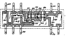
패턴(261,267)를 포함하여 복수개의 도전성 패턴을 기판(260)에 일면 위에 형성한다. 이를 각 패턴은 금도금에 의해 기판위에 형성하는데 금도금의 두께는 약 150미크로인치보다 크다. 그 다음 각 다이리스터 칩(210,211)은 각각 전도성패드(265,264)위에 적절히 납땜해 붙이거나 다른방법으로 부착시켜 알루미나 본체(260)와 양호한 열접촉이 되게한다. 대표적 크기의 장치인 경우 칩(210,211)은 각각 약 82×116밀의 크기를갖는다.A plurality of conductive patterns, including patterns 261 and 267, are formed on one surface of the
LED칩(225)은 도전성 패턴(262)의 일단위에 장착 시킨다. 첩(210,211)은 대체로, 그 양극리이드와 음극리이드가 상호간에 또한 도전성패턴(266,267)의 일단과 일직선상에 놓이도록 실치한다. 따라서 단일와이어(270)를 사용하여 다이리스터(211)의 도전성패드(223)과 다이리스터(210,220)와 도전성패턴(207)의 단부를 전기적으로 연결하면 편리할 것이다. 이것은 고속 자동기술에 적합한 비교적 간단한 방식의 스티치본딩공정으로 행할 수 있다.The
곧, 본딩헤드를 와이어(270)위까지 하강 시키고 패드(223,220)의 위치와 도체(267)의 일단에 일치하는 격치되어 있는 2점에 와이어를 전기적으로 부착 시킨다. 같은 방법으로 둘째의 평행와이어(271)를 도전패드(222,221)과 도전패턴(226)의 단부에 스티치 본딩시킨다. 도체(27)의 스티치본딩을 제 11 도 및 제 12 도에 표시하고 있다. 각 도전와이어(270,271)은 약 6밀의 직경을 가진 알루미늄 와이어면 될 것이다.In other words, the bonding head is lowered up to the wire 270 and the wire is electrically attached to two spaced apart points corresponding to the positions of the pads 223 and 220 and one end of the conductor 267. In the same manner, the second parallel wires 271 are stitch bonded to the ends of the
위의 결과, 전원단자(212,213)은 제 11 도의 다이리스터(210,211)에 제 10 도에서처럼 다이리스터를 서로 역평행관계에 둔채 연결된다.As a result of the above, the
칩(210,211)도 또한 그들 각각의 제어회로를 내포하고 있기 때문에 이 제어회로도 또한 그 자리에서 상기와 같이 단일 스티치 본딩법에 의해 연결하면 된다는 것을 말해 두고자 한다.Since the
LED(225)는, 리이드(226)에 연결되어 있는 도전패턴(262)의 일단의 상부에 배치되어 있음을 볼 수 있다. LED(225)의 다른 극은 와이어(280)에 의해 도전패턴(261)의 일단에 전기적으로 연결되어 있다.It can be seen that the
와이어(280)는 LED(225)의 연장도선이어도 좋은데 이 와이어는 어떤 원하는 방법으로 도전성 패턴(261)의 일단에 본딩된다. 그다음 도전패턴(261)을 와이어(281)의 직접 단락 접속에 의해서 또는 저항(282)에 의해 격치된 도전패턴(263)에 연결한다.Wire 280 may be an extension of
단락 와이어(281) 또는 저항(282)은 단자(226,227)의 전력과 LED(225)의 특성에 따라 적당히 선택한다. 와이어(280,281)는 직경 약 1밀의 금선이면 좋을 것이다. 리이드(212,213,226 및 227)은 기판(260)의 주변에서부터 뻗어나와 이중 인라인핀형 패키지를 구성한다. 그다음 광학적 캡 또는 덮개(291)를 LED(225)와 다이리스터(210,211)위에 배치하여 제 11 도에서 점선(290)으로 표시된 영역을 둘러싼다.The shorting wire 281 or the resistor 282 is appropriately selected depending on the power of the terminals 226 and 227 and the characteristics of the
이 캡은 제 13 도와 제 14 도에서 캡(291)으로 표시되어 있는데, 장치 작동시 발생하는 열에 견딜 수 있는 어떤 원하는 반사경 플라스틱 재료로 만들 수 있다.This cap is shown as
흰색 플라스틱을 실제 사용했다. 플라스틱은 디술폰으로 만들어진 것을 사용하면 좋을 것이다. 플라스틱은 그 내부표면에서 반사할 수 있도록 흰색인 것이 바람직하다. 캡은 또는 산화티탄분말이 혼합된 RTV와 같은 적절한 실리콘으로 만들수도 있다.I actually used white plastic. Plastic may be made of disulfone. The plastic is preferably white so that it can reflect off its inner surface. The cap can also be made of suitable silicon, such as RTV mixed with titanium oxide powder.
산화티탄분말은 실리콘내에 분산상태로 남아있다. 이 혼합물은 약 115℃에서 약 15분간 오븐내에서 경화시킬 수 있다. 캡(291)은 LED(225)의 위치위에 경사면(292)을 갖고 있으며 이 경사면은 제 13 도에서 볼수있는 것처럼 빛을 칩(210,211)의 부분쪽으로 반사할 수 있다.Titanium oxide powder remains dispersed in silicon. This mixture can be cured in an oven at about 115 ° C. for about 15 minutes. The
캡(291)은 제 13 도에 표시한 것처럼 그 자리에서 고정시킬 수도 있고 또는 요구한 대로 기판에 겹치게 배치하여 기판가장자리 위로 스냅 하도록 배치시킬 수 있다.
그 다음에는 제 13 도 및 제 14 도에 충전공(294,294)를 통하여 캡(292)의 내부에 투명한 실리콘을 충전하여 모든 칩(225,210,211)과 거기 연결된 도선을 완전히 인캡슐리션화 하는데 그래도 LED(225)로 부터의 조사광은 댜이리스터 칩(210,211)의 감광성면에 도달하게 된다.Next, the transparent silicon is filled in the
캡(291)을 위치 고정하고 실리콘을 채운 후에, 캡(291)이 부착된 기판(260)전체를 리이드(212,213,226 및 227)이 있는 리이드 프레임내에 장착할 수 있다. 그 다음에는 그 조립된 장치를, 예컨데 이송성형법등으로 만든 하우징내에 완전히 장입한다. 리이드(212,213,226 및 227)은 이 포장체로 부터 뻗쳐나오고 비교적 크기와 부피가 작은 이중, 인라인 핀 패키지가 얻어진다. 그러나 이 창치는 240볼트 a,c에서 1 내지 1/2암페어의 연속 전류정격을 감당할 수 있다.After the
본 발명은 그 바람직한 실시예에 관해서 설명 하였지만 많은 변형과 수식이 당분야에 숙달된자에게는 용이할 것이다. 따라서 본 발명은 여기에 기재된 특정내용에만 한정되는 것이 아니라 오직 첨부된 특허청구의 범위에 의해서만 한정되는 것이 마땅할 것이다.While the invention has been described in terms of its preferred embodiments, many variations and modifications will be readily apparent to those skilled in the art. Therefore, the present invention should not be limited to the specific details described herein but only by the scope of the appended claims.
Claims (31)
Applications Claiming Priority (4)
| Application Number | Priority Date | Filing Date | Title |
|---|---|---|---|
| US06/451,792 US4535251A (en) | 1982-12-21 | 1982-12-21 | A.C. Solid state relay circuit and structure |
| US55502583A | 1983-11-25 | 1983-11-25 | |
| US555025 | 1983-11-25 | ||
| US451792 | 1999-12-01 |
Publications (2)
| Publication Number | Publication Date |
|---|---|
| KR840007203A KR840007203A (en) | 1984-12-05 |
| KR900004197B1 true KR900004197B1 (en) | 1990-06-18 |
Family
ID=27036523
Family Applications (1)
| Application Number | Title | Priority Date | Filing Date |
|---|---|---|---|
| KR1019830006040A KR900004197B1 (en) | 1982-12-21 | 1983-12-20 | A.c. solid state relay circuit and structure |
Country Status (12)
| Country | Link |
|---|---|
| KR (1) | KR900004197B1 (en) |
| BR (1) | BR8307043A (en) |
| CA (1) | CA1237170A (en) |
| CH (1) | CH664861A5 (en) |
| DE (1) | DE3345449A1 (en) |
| FR (1) | FR2538170B1 (en) |
| GB (2) | GB2133641B (en) |
| IL (1) | IL70462A (en) |
| IT (1) | IT1194526B (en) |
| MX (2) | MX160049A (en) |
| NL (1) | NL8304376A (en) |
| SE (1) | SE8306952L (en) |
Families Citing this family (7)
| Publication number | Priority date | Publication date | Assignee | Title |
|---|---|---|---|---|
| FR2590750B1 (en) * | 1985-11-22 | 1991-05-10 | Telemecanique Electrique | SEMICONDUCTOR POWER SWITCHING DEVICE AND ITS USE FOR REALIZING A STATIC RELAY IN AC |
| GB2234642A (en) * | 1989-07-19 | 1991-02-06 | Philips Nv | Protection for a switched bridge circuit |
| GB2241827B (en) * | 1990-02-23 | 1994-01-26 | Matsushita Electric Works Ltd | Method for manufacturing optically triggered lateral thyristor |
| GB2254730B (en) * | 1991-04-08 | 1994-09-21 | Champion Spark Plug Europ | High current photosensitive electronic switch |
| JP3495847B2 (en) * | 1995-09-11 | 2004-02-09 | シャープ株式会社 | Semiconductor integrated circuit with thyristor |
| US6518604B1 (en) | 2000-09-21 | 2003-02-11 | Conexant Systems, Inc. | Diode with variable width metal stripes for improved protection against electrostatic discharge (ESD) current failure |
| EP3249815B1 (en) * | 2016-05-23 | 2019-08-28 | NXP USA, Inc. | Circuit arrangement for fast turn-off of bi-directional switching device |
Family Cites Families (9)
| Publication number | Priority date | Publication date | Assignee | Title |
|---|---|---|---|---|
| JPS5416839B2 (en) * | 1973-03-06 | 1979-06-25 | ||
| US4001867A (en) * | 1974-08-22 | 1977-01-04 | Dionics, Inc. | Semiconductive devices with integrated circuit switches |
| JPS5574168A (en) * | 1978-11-28 | 1980-06-04 | Oki Electric Ind Co Ltd | Pnpn switch |
| DE2932969A1 (en) * | 1979-04-20 | 1980-10-30 | Ske | Semiconductor relay circuit on single chip - uses two LED's isolated from remainder of circuit and optically excited thyristors |
| DE2922250A1 (en) * | 1979-05-31 | 1980-12-11 | Siemens Ag | LIGHT CONTROLLED TRANSISTOR |
| US4295058A (en) * | 1979-06-07 | 1981-10-13 | Eaton Corporation | Radiant energy activated semiconductor switch |
| DE3019907A1 (en) * | 1980-05-23 | 1981-12-03 | Siemens AG, 1000 Berlin und 8000 München | LIGHT-CONTROLLED TWO-WAY THYRISTOR |
| FR2488046A1 (en) * | 1980-07-31 | 1982-02-05 | Silicium Semiconducteur Ssc | DMOS controlled semiconductor power device - uses DMOS FET to drive thyristor with photodiodes deposited on insulating layer with power device using most of substrate area |
| US4361798A (en) * | 1980-10-27 | 1982-11-30 | Pitney Bowes Inc. | System for extending the voltage range of a phase-fired triac controller |
-
1983
- 1983-12-15 DE DE19833345449 patent/DE3345449A1/en active Granted
- 1983-12-15 SE SE8306952A patent/SE8306952L/en not_active Application Discontinuation
- 1983-12-15 IL IL70462A patent/IL70462A/en unknown
- 1983-12-20 CH CH6781/83A patent/CH664861A5/en not_active IP Right Cessation
- 1983-12-20 NL NL8304376A patent/NL8304376A/en not_active Application Discontinuation
- 1983-12-20 KR KR1019830006040A patent/KR900004197B1/en not_active IP Right Cessation
- 1983-12-20 CA CA000443824A patent/CA1237170A/en not_active Expired
- 1983-12-20 IT IT24285/83A patent/IT1194526B/en active
- 1983-12-21 GB GB08333998A patent/GB2133641B/en not_active Expired
- 1983-12-21 MX MX4482A patent/MX160049A/en unknown
- 1983-12-21 MX MX199861A patent/MX155562A/en unknown
- 1983-12-21 FR FR8320500A patent/FR2538170B1/en not_active Expired
- 1983-12-21 BR BR8307043A patent/BR8307043A/en unknown
-
1986
- 1986-02-20 GB GB08604263A patent/GB2174242B/en not_active Expired
Also Published As
| Publication number | Publication date |
|---|---|
| GB2133641A (en) | 1984-07-25 |
| SE8306952L (en) | 1984-06-22 |
| SE8306952D0 (en) | 1983-12-15 |
| GB2174242A (en) | 1986-10-29 |
| IT1194526B (en) | 1988-09-22 |
| GB2133641B (en) | 1986-10-22 |
| IL70462A (en) | 1987-09-16 |
| MX155562A (en) | 1988-03-25 |
| GB8604263D0 (en) | 1986-03-26 |
| GB8333998D0 (en) | 1984-02-01 |
| CA1237170A (en) | 1988-05-24 |
| IT8324285A0 (en) | 1983-12-20 |
| NL8304376A (en) | 1984-07-16 |
| IT8324285A1 (en) | 1985-06-20 |
| DE3345449C2 (en) | 1989-08-17 |
| CH664861A5 (en) | 1988-03-31 |
| KR840007203A (en) | 1984-12-05 |
| FR2538170B1 (en) | 1988-05-27 |
| IL70462A0 (en) | 1984-03-30 |
| GB2174242B (en) | 1987-06-10 |
| BR8307043A (en) | 1984-07-31 |
| FR2538170A1 (en) | 1984-06-22 |
| MX160049A (en) | 1989-11-13 |
| DE3345449A1 (en) | 1984-07-12 |
Similar Documents
| Publication | Publication Date | Title |
|---|---|---|
| US4779126A (en) | Optically triggered lateral thyristor with auxiliary region | |
| US4901127A (en) | Circuit including a combined insulated gate bipolar transistor/MOSFET | |
| US4755697A (en) | Bidirectional output semiconductor field effect transistor | |
| US4721986A (en) | Bidirectional output semiconductor field effect transistor and method for its maufacture | |
| US3971056A (en) | Semiconductor temperature switches | |
| JPH0669423A (en) | Semiconductor component | |
| KR920010314B1 (en) | Semiconductor device | |
| US5352915A (en) | Semiconductor component having two integrated insulated gate field effect devices | |
| JPS59151463A (en) | Solid ac relay and light firing thyristor | |
| KR900004197B1 (en) | A.c. solid state relay circuit and structure | |
| US3622845A (en) | Scr with amplified emitter gate | |
| KR900000829B1 (en) | Photo voltage relay | |
| US3508127A (en) | Semiconductor integrated circuits | |
| JPH0117268B2 (en) | ||
| US4914045A (en) | Method of fabricating packaged TRIAC and trigger switch | |
| RU2137255C1 (en) | High-voltage polarity-reversing diode | |
| US5594261A (en) | Device for isolating parallel sub-elements with reverse conducting diode regions | |
| US4216488A (en) | Lateral semiconductor diac | |
| US4292646A (en) | Semiconductor thyristor device having integral ballast means | |
| US6995408B2 (en) | Bidirectional photothyristor chip | |
| EP0190162B1 (en) | Controlled turn-on thyristor | |
| US5614737A (en) | MOS-controlled high-power thyristor | |
| US4908687A (en) | Controlled turn-on thyristor | |
| US5497010A (en) | High-voltage semiconductor device | |
| EP0025291A1 (en) | A semiconductor switch device suitable for a.c. power control |
Legal Events
| Date | Code | Title | Description |
|---|---|---|---|
| A201 | Request for examination | ||
| E902 | Notification of reason for refusal | ||
| G160 | Decision to publish patent application | ||
| E701 | Decision to grant or registration of patent right | ||
| GRNT | Written decision to grant | ||
| FPAY | Annual fee payment |
Payment date: 19930518 Year of fee payment: 4 |
|
| LAPS | Lapse due to unpaid annual fee |