KR890004472B1 - Cmos 집적회호 - Google Patents
Cmos 집적회호 Download PDFInfo
- Publication number
- KR890004472B1 KR890004472B1 KR1019850000281A KR850000281A KR890004472B1 KR 890004472 B1 KR890004472 B1 KR 890004472B1 KR 1019850000281 A KR1019850000281 A KR 1019850000281A KR 850000281 A KR850000281 A KR 850000281A KR 890004472 B1 KR890004472 B1 KR 890004472B1
- Authority
- KR
- South Korea
- Prior art keywords
- circuit
- mos transistor
- cmos
- power supply
- integrated circuit
- Prior art date
- Legal status (The legal status is an assumption and is not a legal conclusion. Google has not performed a legal analysis and makes no representation as to the accuracy of the status listed.)
- Expired
Links
Images


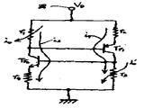
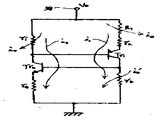


Classifications
-
- H—ELECTRICITY
- H10—SEMICONDUCTOR DEVICES; ELECTRIC SOLID-STATE DEVICES NOT OTHERWISE PROVIDED FOR
- H10D—INORGANIC ELECTRIC SEMICONDUCTOR DEVICES
- H10D84/00—Integrated devices formed in or on semiconductor substrates that comprise only semiconducting layers, e.g. on Si wafers or on GaAs-on-Si wafers
- H10D84/80—Integrated devices formed in or on semiconductor substrates that comprise only semiconducting layers, e.g. on Si wafers or on GaAs-on-Si wafers characterised by the integration of at least one component covered by groups H10D12/00 or H10D30/00, e.g. integration of IGFETs
- H10D84/82—Integrated devices formed in or on semiconductor substrates that comprise only semiconducting layers, e.g. on Si wafers or on GaAs-on-Si wafers characterised by the integration of at least one component covered by groups H10D12/00 or H10D30/00, e.g. integration of IGFETs of only field-effect components
- H10D84/83—Integrated devices formed in or on semiconductor substrates that comprise only semiconducting layers, e.g. on Si wafers or on GaAs-on-Si wafers characterised by the integration of at least one component covered by groups H10D12/00 or H10D30/00, e.g. integration of IGFETs of only field-effect components of only insulated-gate FETs [IGFET]
- H10D84/85—Complementary IGFETs, e.g. CMOS
- H10D84/854—Complementary IGFETs, e.g. CMOS comprising arrangements for preventing bipolar actions between the different IGFET regions, e.g. arrangements for latchup prevention
-
- H—ELECTRICITY
- H10—SEMICONDUCTOR DEVICES; ELECTRIC SOLID-STATE DEVICES NOT OTHERWISE PROVIDED FOR
- H10D—INORGANIC ELECTRIC SEMICONDUCTOR DEVICES
- H10D84/00—Integrated devices formed in or on semiconductor substrates that comprise only semiconducting layers, e.g. on Si wafers or on GaAs-on-Si wafers
- H10D84/80—Integrated devices formed in or on semiconductor substrates that comprise only semiconducting layers, e.g. on Si wafers or on GaAs-on-Si wafers characterised by the integration of at least one component covered by groups H10D12/00 or H10D30/00, e.g. integration of IGFETs
- H10D84/82—Integrated devices formed in or on semiconductor substrates that comprise only semiconducting layers, e.g. on Si wafers or on GaAs-on-Si wafers characterised by the integration of at least one component covered by groups H10D12/00 or H10D30/00, e.g. integration of IGFETs of only field-effect components
- H10D84/83—Integrated devices formed in or on semiconductor substrates that comprise only semiconducting layers, e.g. on Si wafers or on GaAs-on-Si wafers characterised by the integration of at least one component covered by groups H10D12/00 or H10D30/00, e.g. integration of IGFETs of only field-effect components of only insulated-gate FETs [IGFET]
- H10D84/85—Complementary IGFETs, e.g. CMOS
- H10D84/859—Complementary IGFETs, e.g. CMOS comprising both N-type and P-type wells, e.g. twin-tub
-
- H—ELECTRICITY
- H10—SEMICONDUCTOR DEVICES; ELECTRIC SOLID-STATE DEVICES NOT OTHERWISE PROVIDED FOR
- H10D—INORGANIC ELECTRIC SEMICONDUCTOR DEVICES
- H10D84/00—Integrated devices formed in or on semiconductor substrates that comprise only semiconducting layers, e.g. on Si wafers or on GaAs-on-Si wafers
- H10D84/201—Integrated devices formed in or on semiconductor substrates that comprise only semiconducting layers, e.g. on Si wafers or on GaAs-on-Si wafers characterised by the integration of only components covered by H10D1/00 or H10D8/00, e.g. RLC circuits
- H10D84/204—Integrated devices formed in or on semiconductor substrates that comprise only semiconducting layers, e.g. on Si wafers or on GaAs-on-Si wafers characterised by the integration of only components covered by H10D1/00 or H10D8/00, e.g. RLC circuits of combinations of diodes or capacitors or resistors
- H10D84/206—Integrated devices formed in or on semiconductor substrates that comprise only semiconducting layers, e.g. on Si wafers or on GaAs-on-Si wafers characterised by the integration of only components covered by H10D1/00 or H10D8/00, e.g. RLC circuits of combinations of diodes or capacitors or resistors of combinations of capacitors and resistors
Landscapes
- Metal-Oxide And Bipolar Metal-Oxide Semiconductor Integrated Circuits (AREA)
- Semiconductor Integrated Circuits (AREA)
Applications Claiming Priority (3)
| Application Number | Priority Date | Filing Date | Title |
|---|---|---|---|
| JP85-281 | 1984-01-20 | ||
| JP59008721A JPS60152055A (ja) | 1984-01-20 | 1984-01-20 | 相補型mos半導体装置 |
| JP8721 | 1984-01-20 |
Publications (2)
| Publication Number | Publication Date |
|---|---|
| KR850005736A KR850005736A (ko) | 1985-08-28 |
| KR890004472B1 true KR890004472B1 (ko) | 1989-11-04 |
Family
ID=11700810
Family Applications (1)
| Application Number | Title | Priority Date | Filing Date |
|---|---|---|---|
| KR1019850000281A Expired KR890004472B1 (ko) | 1984-01-20 | 1985-01-18 | Cmos 집적회호 |
Country Status (3)
| Country | Link |
|---|---|
| US (1) | US4672584A (https=) |
| JP (1) | JPS60152055A (https=) |
| KR (1) | KR890004472B1 (https=) |
Families Citing this family (27)
| Publication number | Priority date | Publication date | Assignee | Title |
|---|---|---|---|---|
| JPS60231356A (ja) * | 1984-04-28 | 1985-11-16 | Mitsubishi Electric Corp | 相補形金属酸化膜半導体集積回路装置 |
| US4908688A (en) * | 1986-03-14 | 1990-03-13 | Motorola, Inc. | Means and method for providing contact separation in silicided devices |
| JPS63278248A (ja) * | 1987-03-13 | 1988-11-15 | Fujitsu Ltd | ゲ−トアレイの基本セル |
| JP2722453B2 (ja) * | 1987-06-08 | 1998-03-04 | 三菱電機株式会社 | 半導体装置 |
| JPH0713871B2 (ja) * | 1987-06-11 | 1995-02-15 | 三菱電機株式会社 | ダイナミツクram |
| JPS648659A (en) * | 1987-06-30 | 1989-01-12 | Mitsubishi Electric Corp | Supplementary semiconductor integrated circuit device |
| US5117274A (en) * | 1987-10-06 | 1992-05-26 | Motorola, Inc. | Merged complementary bipolar and MOS means and method |
| US4947228A (en) * | 1988-09-20 | 1990-08-07 | At&T Bell Laboratories | Integrated circuit power supply contact |
| US5274262A (en) * | 1989-05-17 | 1993-12-28 | David Sarnoff Research Center, Inc. | SCR protection structure and circuit with reduced trigger voltage |
| US5072273A (en) * | 1990-05-04 | 1991-12-10 | David Sarnoff Research Center, Inc. | Low trigger voltage SCR protection device and structure |
| US5003362A (en) * | 1989-07-28 | 1991-03-26 | Dallas Semiconductor Corporation | Integrated circuit with high-impedance well tie |
| US5021858A (en) * | 1990-05-25 | 1991-06-04 | Hall John H | Compound modulated integrated transistor structure |
| US5317183A (en) * | 1991-09-03 | 1994-05-31 | International Business Machines Corporation | Substrate noise coupling reduction for VLSI applications with mixed analog and digital circuitry |
| JP3184298B2 (ja) * | 1992-05-28 | 2001-07-09 | 沖電気工業株式会社 | Cmos出力回路 |
| JPH09199607A (ja) * | 1996-01-18 | 1997-07-31 | Nec Corp | Cmos半導体装置 |
| US5883566A (en) * | 1997-02-24 | 1999-03-16 | International Business Machines Corporation | Noise-isolated buried resistor |
| GB2394833B (en) * | 2000-08-11 | 2005-03-16 | Samsung Electronics Co Ltd | Protection device with a silicon controlled rectifier |
| US7132696B2 (en) | 2002-08-28 | 2006-11-07 | Micron Technology, Inc. | Intermeshed guard bands for multiple voltage supply structures on an integrated circuit, and methods of making same |
| US7773442B2 (en) * | 2004-06-25 | 2010-08-10 | Cypress Semiconductor Corporation | Memory cell array latchup prevention |
| US9842629B2 (en) | 2004-06-25 | 2017-12-12 | Cypress Semiconductor Corporation | Memory cell array latchup prevention |
| FR2872630B1 (fr) * | 2004-07-01 | 2006-12-01 | St Microelectronics Sa | Circuit integre tolerant au phenomene de verrouillage |
| JP5135815B2 (ja) * | 2006-02-14 | 2013-02-06 | ミツミ電機株式会社 | 半導体集積回路装置 |
| US7834428B2 (en) * | 2007-02-28 | 2010-11-16 | Freescale Semiconductor, Inc. | Apparatus and method for reducing noise in mixed-signal circuits and digital circuits |
| KR102248282B1 (ko) * | 2014-01-21 | 2021-05-06 | 삼성전자주식회사 | Cmos 반도체 장치 |
| US10410934B2 (en) * | 2017-12-07 | 2019-09-10 | Micron Technology, Inc. | Apparatuses having an interconnect extending from an upper conductive structure, through a hole in another conductive structure, and to an underlying structure |
| US10861848B2 (en) * | 2018-08-23 | 2020-12-08 | Xilinx, Inc. | Single event latch-up (SEL) mitigation techniques |
| EP3944316A1 (en) * | 2020-07-21 | 2022-01-26 | Nexperia B.V. | An electrostatic discharge protection semiconductor structure and a method of manufacture |
Family Cites Families (3)
| Publication number | Priority date | Publication date | Assignee | Title |
|---|---|---|---|---|
| JPS5910587B2 (ja) * | 1977-08-10 | 1984-03-09 | 株式会社日立製作所 | 半導体装置の保護装置 |
| JPS5939904B2 (ja) * | 1978-09-28 | 1984-09-27 | 株式会社東芝 | 半導体装置 |
| JPS6046545B2 (ja) * | 1980-05-16 | 1985-10-16 | 日本電気株式会社 | 相補型mos記憶回路装置 |
-
1984
- 1984-01-20 JP JP59008721A patent/JPS60152055A/ja active Granted
-
1985
- 1985-01-15 US US06/691,701 patent/US4672584A/en not_active Expired - Lifetime
- 1985-01-18 KR KR1019850000281A patent/KR890004472B1/ko not_active Expired
Also Published As
| Publication number | Publication date |
|---|---|
| JPS60152055A (ja) | 1985-08-10 |
| US4672584A (en) | 1987-06-09 |
| KR850005736A (ko) | 1985-08-28 |
| JPH0315348B2 (https=) | 1991-02-28 |
Similar Documents
| Publication | Publication Date | Title |
|---|---|---|
| KR890004472B1 (ko) | Cmos 집적회호 | |
| US6236087B1 (en) | SCR cell for electrical overstress protection of electronic circuits | |
| US4100561A (en) | Protective circuit for MOS devices | |
| KR0159451B1 (ko) | 반도체장치의 보호회로 | |
| US6365940B1 (en) | High voltage trigger remote-cathode SCR | |
| KR100311578B1 (ko) | 반도체장치 | |
| US6847059B2 (en) | Semiconductor input protection circuit | |
| US6670678B2 (en) | Semiconductor device having ESD protective transistor | |
| US6355513B1 (en) | Asymmetric depletion region for normally off JFET | |
| US5041894A (en) | Integrated circuit with anti latch-up circuit in complementary MOS circuit technology | |
| HK79493A (en) | Integrated circuit of the complementary technique having a substrate bias generator | |
| US5148250A (en) | Bipolar transistor as protective element for integrated circuits | |
| KR100335527B1 (ko) | 정전보호회로로서형성되는반도체소자 | |
| KR860000159B1 (ko) | 반도체 메모리 | |
| JP3559075B2 (ja) | Cmos技術の集積電子回路用の極性反転保護装置 | |
| US4476479A (en) | Semiconductor device with operating voltage coupling region | |
| US6894320B2 (en) | Input protection circuit | |
| US6320229B1 (en) | Semiconductor device | |
| US5880501A (en) | Semiconductor integrated circuit and manufacturing method of the same | |
| CA1289267C (en) | Latchup and electrostatic discharge protection structure | |
| JPH1117198A (ja) | 集積mosパワー・トランジスタを含むコンポーネントのロジック・ウエルの保護 | |
| US4691221A (en) | Monolithically integrated bipolar Darlington circuit | |
| KR890004426B1 (ko) | 씨 모오스 입력 보호회로 | |
| KR930005948B1 (ko) | 래터럴형 반도체장치 | |
| EP0121096A2 (en) | Semiconductor contact structure |
Legal Events
| Date | Code | Title | Description |
|---|---|---|---|
| A201 | Request for examination | ||
| PA0109 | Patent application |
St.27 status event code: A-0-1-A10-A12-nap-PA0109 |
|
| PA0201 | Request for examination |
St.27 status event code: A-1-2-D10-D11-exm-PA0201 |
|
| R17-X000 | Change to representative recorded |
St.27 status event code: A-3-3-R10-R17-oth-X000 |
|
| PG1501 | Laying open of application |
St.27 status event code: A-1-1-Q10-Q12-nap-PG1501 |
|
| G160 | Decision to publish patent application | ||
| PG1605 | Publication of application before grant of patent |
St.27 status event code: A-2-2-Q10-Q13-nap-PG1605 |
|
| E701 | Decision to grant or registration of patent right | ||
| PE0701 | Decision of registration |
St.27 status event code: A-1-2-D10-D22-exm-PE0701 |
|
| GRNT | Written decision to grant | ||
| PR0701 | Registration of establishment |
St.27 status event code: A-2-4-F10-F11-exm-PR0701 |
|
| PR1002 | Payment of registration fee |
St.27 status event code: A-2-2-U10-U11-oth-PR1002 Fee payment year number: 1 |
|
| PR1001 | Payment of annual fee |
St.27 status event code: A-4-4-U10-U11-oth-PR1001 Fee payment year number: 4 |
|
| PR1001 | Payment of annual fee |
St.27 status event code: A-4-4-U10-U11-oth-PR1001 Fee payment year number: 7 |
|
| PR1001 | Payment of annual fee |
St.27 status event code: A-4-4-U10-U11-oth-PR1001 Fee payment year number: 8 |
|
| PR1001 | Payment of annual fee |
St.27 status event code: A-4-4-U10-U11-oth-PR1001 Fee payment year number: 9 |
|
| FPAY | Annual fee payment |
Payment date: 19981027 Year of fee payment: 10 |
|
| PR1001 | Payment of annual fee |
St.27 status event code: A-4-4-U10-U11-oth-PR1001 Fee payment year number: 10 |
|
| PN2301 | Change of applicant |
St.27 status event code: A-5-5-R10-R13-asn-PN2301 St.27 status event code: A-5-5-R10-R11-asn-PN2301 |
|
| R18-X000 | Changes to party contact information recorded |
St.27 status event code: A-5-5-R10-R18-oth-X000 |
|
| LAPS | Lapse due to unpaid annual fee | ||
| PC1903 | Unpaid annual fee |
St.27 status event code: A-4-4-U10-U13-oth-PC1903 Not in force date: 19991105 Payment event data comment text: Termination Category : DEFAULT_OF_REGISTRATION_FEE |
|
| PC1903 | Unpaid annual fee |
St.27 status event code: N-4-6-H10-H13-oth-PC1903 Ip right cessation event data comment text: Termination Category : DEFAULT_OF_REGISTRATION_FEE Not in force date: 19991105 |
|
| R18-X000 | Changes to party contact information recorded |
St.27 status event code: A-5-5-R10-R18-oth-X000 |
|
| P22-X000 | Classification modified |
St.27 status event code: A-4-4-P10-P22-nap-X000 |
|
| PN2301 | Change of applicant |
St.27 status event code: A-5-5-R10-R13-asn-PN2301 St.27 status event code: A-5-5-R10-R11-asn-PN2301 |
|
| P22-X000 | Classification modified |
St.27 status event code: A-4-4-P10-P22-nap-X000 |
|
| P22-X000 | Classification modified |
St.27 status event code: A-4-4-P10-P22-nap-X000 |