KR20220050737A - 웨이퍼 레벨 테스트를 위한 방법 및 디바이스 - Google Patents
웨이퍼 레벨 테스트를 위한 방법 및 디바이스 Download PDFInfo
- Publication number
- KR20220050737A KR20220050737A KR1020210061308A KR20210061308A KR20220050737A KR 20220050737 A KR20220050737 A KR 20220050737A KR 1020210061308 A KR1020210061308 A KR 1020210061308A KR 20210061308 A KR20210061308 A KR 20210061308A KR 20220050737 A KR20220050737 A KR 20220050737A
- Authority
- KR
- South Korea
- Prior art keywords
- voltage level
- signal
- ramp
- dut
- voltage
- Prior art date
- Legal status (The legal status is an assumption and is not a legal conclusion. Google has not performed a legal analysis and makes no representation as to the accuracy of the status listed.)
- Granted
Links
Images


Classifications
-
- G—PHYSICS
- G01—MEASURING; TESTING
- G01R—MEASURING ELECTRIC VARIABLES; MEASURING MAGNETIC VARIABLES
- G01R31/00—Arrangements for testing electric properties; Arrangements for locating electric faults; Arrangements for electrical testing characterised by what is being tested not provided for elsewhere
- G01R31/28—Testing of electronic circuits, e.g. by signal tracer
- G01R31/317—Testing of digital circuits
- G01R31/31703—Comparison aspects, e.g. signature analysis, comparators
-
- H—ELECTRICITY
- H10—SEMICONDUCTOR DEVICES; ELECTRIC SOLID-STATE DEVICES NOT OTHERWISE PROVIDED FOR
- H10P—GENERIC PROCESSES OR APPARATUS FOR THE MANUFACTURE OR TREATMENT OF DEVICES COVERED BY CLASS H10
- H10P74/00—Testing or measuring during manufacture or treatment of wafers, substrates or devices
- H10P74/20—Testing or measuring during manufacture or treatment of wafers, substrates or devices characterised by the properties tested or measured, e.g. structural or electrical properties
- H10P74/207—Electrical properties, e.g. testing or measuring of resistance, deep levels or capacitance-voltage characteristics
-
- H—ELECTRICITY
- H10—SEMICONDUCTOR DEVICES; ELECTRIC SOLID-STATE DEVICES NOT OTHERWISE PROVIDED FOR
- H10P—GENERIC PROCESSES OR APPARATUS FOR THE MANUFACTURE OR TREATMENT OF DEVICES COVERED BY CLASS H10
- H10P74/00—Testing or measuring during manufacture or treatment of wafers, substrates or devices
- H10P74/20—Testing or measuring during manufacture or treatment of wafers, substrates or devices characterised by the properties tested or measured, e.g. structural or electrical properties
- H10P74/203—Structural properties, e.g. testing or measuring thicknesses, line widths, warpage, bond strengths or physical defects
-
- G—PHYSICS
- G01—MEASURING; TESTING
- G01R—MEASURING ELECTRIC VARIABLES; MEASURING MAGNETIC VARIABLES
- G01R31/00—Arrangements for testing electric properties; Arrangements for locating electric faults; Arrangements for electrical testing characterised by what is being tested not provided for elsewhere
- G01R31/28—Testing of electronic circuits, e.g. by signal tracer
- G01R31/317—Testing of digital circuits
- G01R31/31712—Input or output aspects
- G01R31/31715—Testing of input or output circuits; test of circuitry between the I/C pins and the functional core, e.g. testing of input or output driver, receiver, buffer
-
- H01L21/823814—
-
- H01L21/823864—
-
- H01L21/823871—
-
- H—ELECTRICITY
- H10—SEMICONDUCTOR DEVICES; ELECTRIC SOLID-STATE DEVICES NOT OTHERWISE PROVIDED FOR
- H10D—INORGANIC ELECTRIC SEMICONDUCTOR DEVICES
- H10D84/00—Integrated devices formed in or on semiconductor substrates that comprise only semiconducting layers, e.g. on Si wafers or on GaAs-on-Si wafers
- H10D84/01—Manufacture or treatment
- H10D84/0123—Integrating together multiple components covered by H10D12/00 or H10D30/00, e.g. integrating multiple IGBTs
- H10D84/0126—Integrating together multiple components covered by H10D12/00 or H10D30/00, e.g. integrating multiple IGBTs the components including insulated gates, e.g. IGFETs
- H10D84/0165—Integrating together multiple components covered by H10D12/00 or H10D30/00, e.g. integrating multiple IGBTs the components including insulated gates, e.g. IGFETs the components including complementary IGFETs, e.g. CMOS devices
- H10D84/017—Manufacturing their source or drain regions, e.g. silicided source or drain regions
-
- H—ELECTRICITY
- H10—SEMICONDUCTOR DEVICES; ELECTRIC SOLID-STATE DEVICES NOT OTHERWISE PROVIDED FOR
- H10D—INORGANIC ELECTRIC SEMICONDUCTOR DEVICES
- H10D84/00—Integrated devices formed in or on semiconductor substrates that comprise only semiconducting layers, e.g. on Si wafers or on GaAs-on-Si wafers
- H10D84/01—Manufacture or treatment
- H10D84/0123—Integrating together multiple components covered by H10D12/00 or H10D30/00, e.g. integrating multiple IGBTs
- H10D84/0126—Integrating together multiple components covered by H10D12/00 or H10D30/00, e.g. integrating multiple IGBTs the components including insulated gates, e.g. IGFETs
- H10D84/0165—Integrating together multiple components covered by H10D12/00 or H10D30/00, e.g. integrating multiple IGBTs the components including insulated gates, e.g. IGFETs the components including complementary IGFETs, e.g. CMOS devices
- H10D84/0184—Manufacturing their gate sidewall spacers
-
- H—ELECTRICITY
- H10—SEMICONDUCTOR DEVICES; ELECTRIC SOLID-STATE DEVICES NOT OTHERWISE PROVIDED FOR
- H10D—INORGANIC ELECTRIC SEMICONDUCTOR DEVICES
- H10D84/00—Integrated devices formed in or on semiconductor substrates that comprise only semiconducting layers, e.g. on Si wafers or on GaAs-on-Si wafers
- H10D84/01—Manufacture or treatment
- H10D84/0123—Integrating together multiple components covered by H10D12/00 or H10D30/00, e.g. integrating multiple IGBTs
- H10D84/0126—Integrating together multiple components covered by H10D12/00 or H10D30/00, e.g. integrating multiple IGBTs the components including insulated gates, e.g. IGFETs
- H10D84/0165—Integrating together multiple components covered by H10D12/00 or H10D30/00, e.g. integrating multiple IGBTs the components including insulated gates, e.g. IGFETs the components including complementary IGFETs, e.g. CMOS devices
- H10D84/0186—Manufacturing their interconnections or electrodes, e.g. source or drain electrodes
-
- H—ELECTRICITY
- H10—SEMICONDUCTOR DEVICES; ELECTRIC SOLID-STATE DEVICES NOT OTHERWISE PROVIDED FOR
- H10P—GENERIC PROCESSES OR APPARATUS FOR THE MANUFACTURE OR TREATMENT OF DEVICES COVERED BY CLASS H10
- H10P74/00—Testing or measuring during manufacture or treatment of wafers, substrates or devices
- H10P74/27—Structural arrangements therefor
- H10P74/273—Interconnections for measuring or testing, e.g. probe pads
-
- G—PHYSICS
- G01—MEASURING; TESTING
- G01R—MEASURING ELECTRIC VARIABLES; MEASURING MAGNETIC VARIABLES
- G01R31/00—Arrangements for testing electric properties; Arrangements for locating electric faults; Arrangements for electrical testing characterised by what is being tested not provided for elsewhere
- G01R31/28—Testing of electronic circuits, e.g. by signal tracer
- G01R31/30—Marginal testing, e.g. by varying supply voltage
- G01R31/3004—Current or voltage test
-
- H—ELECTRICITY
- H10—SEMICONDUCTOR DEVICES; ELECTRIC SOLID-STATE DEVICES NOT OTHERWISE PROVIDED FOR
- H10D—INORGANIC ELECTRIC SEMICONDUCTOR DEVICES
- H10D84/00—Integrated devices formed in or on semiconductor substrates that comprise only semiconducting layers, e.g. on Si wafers or on GaAs-on-Si wafers
- H10D84/80—Integrated devices formed in or on semiconductor substrates that comprise only semiconducting layers, e.g. on Si wafers or on GaAs-on-Si wafers characterised by the integration of at least one component covered by groups H10D12/00 or H10D30/00, e.g. integration of IGFETs
- H10D84/82—Integrated devices formed in or on semiconductor substrates that comprise only semiconducting layers, e.g. on Si wafers or on GaAs-on-Si wafers characterised by the integration of at least one component covered by groups H10D12/00 or H10D30/00, e.g. integration of IGFETs of only field-effect components
- H10D84/83—Integrated devices formed in or on semiconductor substrates that comprise only semiconducting layers, e.g. on Si wafers or on GaAs-on-Si wafers characterised by the integration of at least one component covered by groups H10D12/00 or H10D30/00, e.g. integration of IGFETs of only field-effect components of only insulated-gate FETs [IGFET]
- H10D84/85—Complementary IGFETs, e.g. CMOS
-
- H—ELECTRICITY
- H10—SEMICONDUCTOR DEVICES; ELECTRIC SOLID-STATE DEVICES NOT OTHERWISE PROVIDED FOR
- H10P—GENERIC PROCESSES OR APPARATUS FOR THE MANUFACTURE OR TREATMENT OF DEVICES COVERED BY CLASS H10
- H10P74/00—Testing or measuring during manufacture or treatment of wafers, substrates or devices
- H10P74/23—Testing or measuring during manufacture or treatment of wafers, substrates or devices characterised by multiple measurements, corrections, marking or sorting processes
Landscapes
- Engineering & Computer Science (AREA)
- General Engineering & Computer Science (AREA)
- Physics & Mathematics (AREA)
- General Physics & Mathematics (AREA)
- Testing Or Measuring Of Semiconductors Or The Like (AREA)
Abstract
Description
도 1은 본 개시 내용의 일부 실시예에 따른 반도체 디바이스를 테스트하기 위한 시스템의 개략도이다.
도 2a는 본 개시 내용의 일부 실시예에 따라 웨이퍼를 테스트하기 위한 복수의 스텝 파워 신호의 예시이다.
도 2b는 본 개시 내용의 일부 실시예에 따른 시퀀스의 복수 스텝의 램프-업 및 램프-다운 스테이지의 예시이다.
도 3a는 종래의 동적 전압 스트레스 테스트 방법에서 웨이퍼를 테스트하기 위한 단일 스텝 파워 신호의 예시이다.
도 3b는 종래의 상승 전압 스트레스 테스트 방법에서 웨이퍼를 테스트하기 위한 단일 스텝 파워 신호의 예시이다.
도 4는 본 개시 내용의 일부 실시예에 따라 웨이퍼를 테스트하기 위한 복수의 스텝 파워 신호의 예시이다.
도 5는 본 개시 내용의 일부 실시예에 따라 웨이퍼를 테스트하기 위한 복수의 스텝 파워 신호의 예시이다.
도 6은 본 개시 내용의 일부 실시예에 따라 웨이퍼를 테스트하기 위한 복수의 스텝 파워 신호의 예시이다.
도 7은 본 개시 내용의 일부 실시예에 따른 방법을 예시하는 흐름도이다.
도 8은 본 개시 내용의 일부 실시예에 따른 방법을 예시하는 흐름도이다.
도 9는 본 개시 내용의 일부 실시예에 따른 인버터 회로의 예시이다.
도 10은 도 9의 실시예에 따른 입력 및 출력 신호의 파형을 나타내는 타이밍 차트이다.
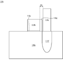
도 11a는 본 개시 내용의 일부 실시예에 따른 반도체 구조물을 예시한다.
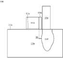
도 11b는 본 개시 내용의 일부 실시예에 따른 반도체 구조물을 예시한다.
Claims (10)
- 방법에 있어서,
입력 단자 및 출력 단자를 가지는 DUT(Device Under Test)를 제공하는 단계;
제1 기간 동안 상기 DUT의 입력 단자에 제1 전압 레벨을 가지는 전압을 인가하는 단계;
제1 기간 이후의 제2 기간 동안 상기 DUT의 입력 단자에 스트레스(stress) 신호를 인가하는 단계 - 상기 스트레스 신호는 복수의 시퀀스를 포함하며, 상기 시퀀스의 각각은 램프-업(ramp-up) 스테이지 및 램프-다운(ramp-down) 스테이지를 가지며, 상기 스트레스 신호는 제2 전압 레벨 및 제3 전압 레벨을 가짐 -;
상기 DUT의 출력 단자에서 상기 스트레스 신호에 응답하여 출력 신호를 획득하는 단계; 및
상기 출력 신호를 상기 스트레스 신호와 비교하는 단계
를 포함하는 방법. - 제1항에 있어서, 상기 출력 신호와 상기 스트레스 신호 간의 비교 결과에 기초하여 상기 DUT가 비정상적인(abnormal) 구조를 갖는지 여부를 결정하는 단계를 더 포함하는 방법.
- 제2항에 있어서, 상기 DUT는 동일한 시간 영역에서 상기 출력 신호가 상기 스트레스 신호와 논리적으로 상이한 경우에 비정상적인 구조를 갖는 것으로 결정되는 것인 방법.
- 제1항에 있어서, 상기 DUT는,
상기 DUT의 입력 단자에 연결되는 소스, 게이트, 및 상기 DUT의 출력 단자에 연결되는 드레인을 가지는 PMOS; 및
접지에 연결되는 소스, 상기 PMOS의 상기 게이트에 연결되는 게이트, 및 상기 DUT의 출력 단자에 연결되는 드레인을 가지는 NMOS
를 포함하는 방법. - 방법에 있어서,
입력 단자 및 출력 단자를 가지는 DUT를 제공하는 단계;
상기 DUT의 입력 단자에 스트레스 신호를 인가하는 단계;
상기 DUT의 출력 단자에서 상기 스트레스 신호에 응답하여 출력 신호를 획득하는 단계 - 상기 출력 신호는 복수의 시퀀스를 포함하며, 상기 시퀀스의 각각은 램프-업 스테이지 및 램프-다운 스테이지를 가지며, 상기 출력 신호는 제1 전압 레벨 및 제2 전압 레벨을 가짐 -;
상기 출력 신호를 상기 스트레스 신호와 비교하는 단계; 및
상기 출력 신호와 상기 스트레스 신호 간의 비교 결과에 기초하여 상기 DUT가 비정상적인 구조를 갖는지 여부를 결정하는 단계
를 포함하는 방법. - 반도체 디바이스로서,
스트레스 신호를 수신하도록 구성된 제1 입력 단자;
상기 스트레스 신호에 응답하여 출력 신호를 생성하도록 구성된 출력 단자;
기판;
상기 기판 상에 배치된 게이트; 및
상기 기판 상에 그리고 상기 게이트 옆에 배치된 콘택 - 상기 콘택은 상기 제1 입력 단자 또는 상기 출력 단자에 전기적으로 연결되고, 상기 게이트와 상기 콘택 사이의 거리가 3 나노미터(nm) 미만임 -
을 포함하는 반도체 디바이스. - 제6항에 있어서, 상기 기판 내에 그리고 상기 콘택 아래에 배치된 에피택시를 더 포함하고, 상기 기판 상의 게이트의 투사(projection) 라인과 상기 기판 상의 에피택시의 투사 라인 사이의 최소 거리는 1 nm 미만인 반도체 디바이스.
- 제6항에 있어서,
상기 기판 상에 그리고 상기 게이트와 상기 콘택 사이에 배치된 스페이서; 및
상기 게이트와 상기 기판 사이에 배치된 게이트 유전체
를 더 포함하는 반도체 디바이스. - 제6항에 있어서, 상기 스트레스 신호에 응답하는 상기 출력 신호는 복수의 시퀀스를 포함하고, 상기 시퀀스의 각각은 램프-업 스테이지 및 램프-다운 스테이지를 가지며, 상기 출력 신호는 제1 전압 레벨 및 제2 전압 레벨을 가지는 것인 반도체 디바이스.
- 제9항에 있어서, 상기 반도체 디바이스의 상기 제1 입력 단자는 또한, 상기 스트레스 신호를 수신하기 전에 제3 전압 레벨을 가지는 전압을 수신하도록 구성되는 것인 반도체 디바이스.
Applications Claiming Priority (6)
| Application Number | Priority Date | Filing Date | Title |
|---|---|---|---|
| US202063092743P | 2020-10-16 | 2020-10-16 | |
| US63/092,743 | 2020-10-16 | ||
| US202063115280P | 2020-11-18 | 2020-11-18 | |
| US63/115,280 | 2020-11-18 | ||
| US17/198,764 | 2021-03-11 | ||
| US17/198,764 US11448692B2 (en) | 2018-08-16 | 2021-03-11 | Method and device for wafer-level testing |
Publications (2)
| Publication Number | Publication Date |
|---|---|
| KR20220050737A true KR20220050737A (ko) | 2022-04-25 |
| KR102590203B1 KR102590203B1 (ko) | 2023-10-16 |
Family
ID=80929234
Family Applications (1)
| Application Number | Title | Priority Date | Filing Date |
|---|---|---|---|
| KR1020210061308A Active KR102590203B1 (ko) | 2020-10-16 | 2021-05-12 | 웨이퍼 레벨 테스트를 위한 방법 및 디바이스 |
Country Status (4)
| Country | Link |
|---|---|
| KR (1) | KR102590203B1 (ko) |
| CN (1) | CN114373691A (ko) |
| DE (1) | DE102021106795A1 (ko) |
| TW (1) | TWI775435B (ko) |
Families Citing this family (1)
| Publication number | Priority date | Publication date | Assignee | Title |
|---|---|---|---|---|
| CN111983421B (zh) * | 2019-05-24 | 2023-07-25 | 台湾积体电路制造股份有限公司 | 电路检测系统与电路检测方法 |
Citations (12)
| Publication number | Priority date | Publication date | Assignee | Title |
|---|---|---|---|---|
| EP0348099A2 (en) * | 1988-06-21 | 1989-12-27 | AT&T Corp. | Floating gate memories |
| KR20000026475A (ko) * | 1998-10-20 | 2000-05-15 | 윤종용 | 파워 온 리셋 회로를 가지는 테스트 회로 |
| KR20030089021A (ko) * | 2002-05-15 | 2003-11-21 | 삼성전자주식회사 | 테스트 소자 그룹 회로를 포함하는 집적 회로 칩 및그것의 제조 방법 |
| US20060234398A1 (en) * | 2005-04-15 | 2006-10-19 | International Business Machines Corporation | Single ic-chip design on wafer with an embedded sensor utilizing rf capabilities to enable real-time data transmission |
| US20090167339A1 (en) * | 2007-12-31 | 2009-07-02 | Andrew Marshall | Contactless Testing of Wafer Characteristics |
| US20100182859A1 (en) * | 2007-10-29 | 2010-07-22 | Kohler Ross A | Method and Apparatus for Testing a Memory Device |
| US20110037494A1 (en) * | 2009-08-11 | 2011-02-17 | Taiwan Semiconductor Manufacturing Company, Ltd. | Method for Wafer-Level Testing of Integrated Circuits |
| KR20110021892A (ko) * | 2008-05-15 | 2011-03-04 | 퀄컴 인코포레이티드 | 바이어스 온도 불안정성에 의해 야기된 임계 전압 시프트를 경험하는 전계 효과 트랜지스터를 갖는 메모리 디바이스의 테스팅 |
| KR20140031075A (ko) * | 2012-09-04 | 2014-03-12 | 타이완 세미콘덕터 매뉴팩쳐링 컴퍼니 리미티드 | 툴 상태 모니터링을 위한 정성적 고장 검출 및 분류 시스템 및 연관된 방법 |
| KR20150073460A (ko) * | 2013-12-23 | 2015-07-01 | 엘지디스플레이 주식회사 | 표시장치의 테스트장치 |
| US9176167B1 (en) * | 2011-08-21 | 2015-11-03 | Bruker Nano Inc. | Probe and method of manufacture for semiconductor wafer characterization |
| US20170350938A1 (en) * | 2016-06-01 | 2017-12-07 | Taiwan Semiconductor Manufacturing Co., Ltd. | Ic degradation management circuit, system and method |
Family Cites Families (6)
| Publication number | Priority date | Publication date | Assignee | Title |
|---|---|---|---|---|
| US4853561A (en) * | 1987-06-10 | 1989-08-01 | Regents Of The University Of Minnesota | Family of noise-immune logic gates and memory cells |
| JPH07288463A (ja) * | 1994-04-18 | 1995-10-31 | Nec Corp | BiCMOS半導体集積回路 |
| JP3391249B2 (ja) * | 1998-03-11 | 2003-03-31 | ヤマハ株式会社 | アナログ信号の遅延回路 |
| JP4951907B2 (ja) * | 2005-09-16 | 2012-06-13 | 富士電機株式会社 | 半導体回路、インバータ回路および半導体装置 |
| WO2018190881A1 (en) * | 2017-04-15 | 2018-10-18 | Intel IP Corporation | Multi-drain esd-robust transistor arrangements |
| US11073551B2 (en) * | 2018-08-16 | 2021-07-27 | Taiwan Semiconductor Manufacturing Company Ltd. | Method and system for wafer-level testing |
-
2021
- 2021-03-19 DE DE102021106795.2A patent/DE102021106795A1/de active Pending
- 2021-05-12 KR KR1020210061308A patent/KR102590203B1/ko active Active
- 2021-05-14 TW TW110117581A patent/TWI775435B/zh active
- 2021-06-25 CN CN202110710654.3A patent/CN114373691A/zh active Pending
Patent Citations (13)
| Publication number | Priority date | Publication date | Assignee | Title |
|---|---|---|---|---|
| EP0348099A2 (en) * | 1988-06-21 | 1989-12-27 | AT&T Corp. | Floating gate memories |
| EP0348099B1 (en) * | 1988-06-21 | 1994-08-31 | AT&T Corp. | Floating gate memories |
| KR20000026475A (ko) * | 1998-10-20 | 2000-05-15 | 윤종용 | 파워 온 리셋 회로를 가지는 테스트 회로 |
| KR20030089021A (ko) * | 2002-05-15 | 2003-11-21 | 삼성전자주식회사 | 테스트 소자 그룹 회로를 포함하는 집적 회로 칩 및그것의 제조 방법 |
| US20060234398A1 (en) * | 2005-04-15 | 2006-10-19 | International Business Machines Corporation | Single ic-chip design on wafer with an embedded sensor utilizing rf capabilities to enable real-time data transmission |
| US20100182859A1 (en) * | 2007-10-29 | 2010-07-22 | Kohler Ross A | Method and Apparatus for Testing a Memory Device |
| US20090167339A1 (en) * | 2007-12-31 | 2009-07-02 | Andrew Marshall | Contactless Testing of Wafer Characteristics |
| KR20110021892A (ko) * | 2008-05-15 | 2011-03-04 | 퀄컴 인코포레이티드 | 바이어스 온도 불안정성에 의해 야기된 임계 전압 시프트를 경험하는 전계 효과 트랜지스터를 갖는 메모리 디바이스의 테스팅 |
| US20110037494A1 (en) * | 2009-08-11 | 2011-02-17 | Taiwan Semiconductor Manufacturing Company, Ltd. | Method for Wafer-Level Testing of Integrated Circuits |
| US9176167B1 (en) * | 2011-08-21 | 2015-11-03 | Bruker Nano Inc. | Probe and method of manufacture for semiconductor wafer characterization |
| KR20140031075A (ko) * | 2012-09-04 | 2014-03-12 | 타이완 세미콘덕터 매뉴팩쳐링 컴퍼니 리미티드 | 툴 상태 모니터링을 위한 정성적 고장 검출 및 분류 시스템 및 연관된 방법 |
| KR20150073460A (ko) * | 2013-12-23 | 2015-07-01 | 엘지디스플레이 주식회사 | 표시장치의 테스트장치 |
| US20170350938A1 (en) * | 2016-06-01 | 2017-12-07 | Taiwan Semiconductor Manufacturing Co., Ltd. | Ic degradation management circuit, system and method |
Also Published As
| Publication number | Publication date |
|---|---|
| TW202217996A (zh) | 2022-05-01 |
| TWI775435B (zh) | 2022-08-21 |
| DE102021106795A1 (de) | 2022-04-21 |
| CN114373691A (zh) | 2022-04-19 |
| KR102590203B1 (ko) | 2023-10-16 |
Similar Documents
| Publication | Publication Date | Title |
|---|---|---|
| US12066484B2 (en) | Method and device for wafer-level testing | |
| US6815971B2 (en) | Method and apparatus for stress testing integrated circuits using an adjustable AC hot carrier injection source | |
| US12025655B2 (en) | Method and system for wafer-level testing | |
| KR100466984B1 (ko) | 테스트 소자 그룹 회로를 포함하는 집적 회로 칩 및 그것의 테스트 방법 | |
| US8004297B2 (en) | Isolation circuit | |
| US11573261B2 (en) | Semiconductor device and method of operating the same | |
| KR102590203B1 (ko) | 웨이퍼 레벨 테스트를 위한 방법 및 디바이스 | |
| US6950355B2 (en) | System and method to screen defect related reliability failures in CMOS SRAMS | |
| KR100576492B1 (ko) | 패키지 레벨에서 반도체 소자의 내부 dc 바이어스 측정장치 | |
| US20250383394A1 (en) | Time-dependent dielectric breakdown (tddb) test unit, measurement circuit and method thereof | |
| US12044723B2 (en) | Circuit for temperature stress test for memory chips | |
| JP2954076B2 (ja) | 半導体集積回路ウェハ及びその試験方法 | |
| KR100934793B1 (ko) | 반도체 소자 테스트 방법 및 그 장치, 적정 스트레스 전압검출 방법 | |
| Sim et al. | A case study on different test screening techniques for ICS with high resistance vias interconnects issues | |
| KR20080088676A (ko) | 반도체 소자의 테스트 장치 |
Legal Events
| Date | Code | Title | Description |
|---|---|---|---|
| PA0109 | Patent application |
Patent event code: PA01091R01D Comment text: Patent Application Patent event date: 20210512 |
|
| PA0201 | Request for examination | ||
| PG1501 | Laying open of application | ||
| E902 | Notification of reason for refusal | ||
| PE0902 | Notice of grounds for rejection |
Comment text: Notification of reason for refusal Patent event date: 20230215 Patent event code: PE09021S01D |
|
| E701 | Decision to grant or registration of patent right | ||
| PE0701 | Decision of registration |
Patent event code: PE07011S01D Comment text: Decision to Grant Registration Patent event date: 20230718 |
|
| GRNT | Written decision to grant | ||
| PR0701 | Registration of establishment |
Comment text: Registration of Establishment Patent event date: 20231012 Patent event code: PR07011E01D |
|
| PR1002 | Payment of registration fee |
Payment date: 20231012 End annual number: 3 Start annual number: 1 |
|
| PG1601 | Publication of registration |