KR20220050737A - Method and device for wafer-level testing - Google Patents
Method and device for wafer-level testing Download PDFInfo
- Publication number
- KR20220050737A KR20220050737A KR1020210061308A KR20210061308A KR20220050737A KR 20220050737 A KR20220050737 A KR 20220050737A KR 1020210061308 A KR1020210061308 A KR 1020210061308A KR 20210061308 A KR20210061308 A KR 20210061308A KR 20220050737 A KR20220050737 A KR 20220050737A
- Authority
- KR
- South Korea
- Prior art keywords
- voltage level
- signal
- ramp
- dut
- voltage
- Prior art date
- Legal status (The legal status is an assumption and is not a legal conclusion. Google has not performed a legal analysis and makes no representation as to the accuracy of the status listed.)
- Granted
Links
Images


Classifications
-
- G—PHYSICS
- G01—MEASURING; TESTING
- G01R—MEASURING ELECTRIC VARIABLES; MEASURING MAGNETIC VARIABLES
- G01R31/00—Arrangements for testing electric properties; Arrangements for locating electric faults; Arrangements for electrical testing characterised by what is being tested not provided for elsewhere
- G01R31/28—Testing of electronic circuits, e.g. by signal tracer
- G01R31/317—Testing of digital circuits
- G01R31/31703—Comparison aspects, e.g. signature analysis, comparators
-
- H—ELECTRICITY
- H10—SEMICONDUCTOR DEVICES; ELECTRIC SOLID-STATE DEVICES NOT OTHERWISE PROVIDED FOR
- H10P—GENERIC PROCESSES OR APPARATUS FOR THE MANUFACTURE OR TREATMENT OF DEVICES COVERED BY CLASS H10
- H10P74/00—Testing or measuring during manufacture or treatment of wafers, substrates or devices
- H10P74/20—Testing or measuring during manufacture or treatment of wafers, substrates or devices characterised by the properties tested or measured, e.g. structural or electrical properties
- H10P74/207—Electrical properties, e.g. testing or measuring of resistance, deep levels or capacitance-voltage characteristics
-
- H—ELECTRICITY
- H10—SEMICONDUCTOR DEVICES; ELECTRIC SOLID-STATE DEVICES NOT OTHERWISE PROVIDED FOR
- H10P—GENERIC PROCESSES OR APPARATUS FOR THE MANUFACTURE OR TREATMENT OF DEVICES COVERED BY CLASS H10
- H10P74/00—Testing or measuring during manufacture or treatment of wafers, substrates or devices
- H10P74/20—Testing or measuring during manufacture or treatment of wafers, substrates or devices characterised by the properties tested or measured, e.g. structural or electrical properties
- H10P74/203—Structural properties, e.g. testing or measuring thicknesses, line widths, warpage, bond strengths or physical defects
-
- G—PHYSICS
- G01—MEASURING; TESTING
- G01R—MEASURING ELECTRIC VARIABLES; MEASURING MAGNETIC VARIABLES
- G01R31/00—Arrangements for testing electric properties; Arrangements for locating electric faults; Arrangements for electrical testing characterised by what is being tested not provided for elsewhere
- G01R31/28—Testing of electronic circuits, e.g. by signal tracer
- G01R31/317—Testing of digital circuits
- G01R31/31712—Input or output aspects
- G01R31/31715—Testing of input or output circuits; test of circuitry between the I/C pins and the functional core, e.g. testing of input or output driver, receiver, buffer
-
- H01L21/823814—
-
- H01L21/823864—
-
- H01L21/823871—
-
- H—ELECTRICITY
- H10—SEMICONDUCTOR DEVICES; ELECTRIC SOLID-STATE DEVICES NOT OTHERWISE PROVIDED FOR
- H10D—INORGANIC ELECTRIC SEMICONDUCTOR DEVICES
- H10D84/00—Integrated devices formed in or on semiconductor substrates that comprise only semiconducting layers, e.g. on Si wafers or on GaAs-on-Si wafers
- H10D84/01—Manufacture or treatment
- H10D84/0123—Integrating together multiple components covered by H10D12/00 or H10D30/00, e.g. integrating multiple IGBTs
- H10D84/0126—Integrating together multiple components covered by H10D12/00 or H10D30/00, e.g. integrating multiple IGBTs the components including insulated gates, e.g. IGFETs
- H10D84/0165—Integrating together multiple components covered by H10D12/00 or H10D30/00, e.g. integrating multiple IGBTs the components including insulated gates, e.g. IGFETs the components including complementary IGFETs, e.g. CMOS devices
- H10D84/017—Manufacturing their source or drain regions, e.g. silicided source or drain regions
-
- H—ELECTRICITY
- H10—SEMICONDUCTOR DEVICES; ELECTRIC SOLID-STATE DEVICES NOT OTHERWISE PROVIDED FOR
- H10D—INORGANIC ELECTRIC SEMICONDUCTOR DEVICES
- H10D84/00—Integrated devices formed in or on semiconductor substrates that comprise only semiconducting layers, e.g. on Si wafers or on GaAs-on-Si wafers
- H10D84/01—Manufacture or treatment
- H10D84/0123—Integrating together multiple components covered by H10D12/00 or H10D30/00, e.g. integrating multiple IGBTs
- H10D84/0126—Integrating together multiple components covered by H10D12/00 or H10D30/00, e.g. integrating multiple IGBTs the components including insulated gates, e.g. IGFETs
- H10D84/0165—Integrating together multiple components covered by H10D12/00 or H10D30/00, e.g. integrating multiple IGBTs the components including insulated gates, e.g. IGFETs the components including complementary IGFETs, e.g. CMOS devices
- H10D84/0184—Manufacturing their gate sidewall spacers
-
- H—ELECTRICITY
- H10—SEMICONDUCTOR DEVICES; ELECTRIC SOLID-STATE DEVICES NOT OTHERWISE PROVIDED FOR
- H10D—INORGANIC ELECTRIC SEMICONDUCTOR DEVICES
- H10D84/00—Integrated devices formed in or on semiconductor substrates that comprise only semiconducting layers, e.g. on Si wafers or on GaAs-on-Si wafers
- H10D84/01—Manufacture or treatment
- H10D84/0123—Integrating together multiple components covered by H10D12/00 or H10D30/00, e.g. integrating multiple IGBTs
- H10D84/0126—Integrating together multiple components covered by H10D12/00 or H10D30/00, e.g. integrating multiple IGBTs the components including insulated gates, e.g. IGFETs
- H10D84/0165—Integrating together multiple components covered by H10D12/00 or H10D30/00, e.g. integrating multiple IGBTs the components including insulated gates, e.g. IGFETs the components including complementary IGFETs, e.g. CMOS devices
- H10D84/0186—Manufacturing their interconnections or electrodes, e.g. source or drain electrodes
-
- H—ELECTRICITY
- H10—SEMICONDUCTOR DEVICES; ELECTRIC SOLID-STATE DEVICES NOT OTHERWISE PROVIDED FOR
- H10P—GENERIC PROCESSES OR APPARATUS FOR THE MANUFACTURE OR TREATMENT OF DEVICES COVERED BY CLASS H10
- H10P74/00—Testing or measuring during manufacture or treatment of wafers, substrates or devices
- H10P74/27—Structural arrangements therefor
- H10P74/273—Interconnections for measuring or testing, e.g. probe pads
-
- G—PHYSICS
- G01—MEASURING; TESTING
- G01R—MEASURING ELECTRIC VARIABLES; MEASURING MAGNETIC VARIABLES
- G01R31/00—Arrangements for testing electric properties; Arrangements for locating electric faults; Arrangements for electrical testing characterised by what is being tested not provided for elsewhere
- G01R31/28—Testing of electronic circuits, e.g. by signal tracer
- G01R31/30—Marginal testing, e.g. by varying supply voltage
- G01R31/3004—Current or voltage test
-
- H—ELECTRICITY
- H10—SEMICONDUCTOR DEVICES; ELECTRIC SOLID-STATE DEVICES NOT OTHERWISE PROVIDED FOR
- H10D—INORGANIC ELECTRIC SEMICONDUCTOR DEVICES
- H10D84/00—Integrated devices formed in or on semiconductor substrates that comprise only semiconducting layers, e.g. on Si wafers or on GaAs-on-Si wafers
- H10D84/80—Integrated devices formed in or on semiconductor substrates that comprise only semiconducting layers, e.g. on Si wafers or on GaAs-on-Si wafers characterised by the integration of at least one component covered by groups H10D12/00 or H10D30/00, e.g. integration of IGFETs
- H10D84/82—Integrated devices formed in or on semiconductor substrates that comprise only semiconducting layers, e.g. on Si wafers or on GaAs-on-Si wafers characterised by the integration of at least one component covered by groups H10D12/00 or H10D30/00, e.g. integration of IGFETs of only field-effect components
- H10D84/83—Integrated devices formed in or on semiconductor substrates that comprise only semiconducting layers, e.g. on Si wafers or on GaAs-on-Si wafers characterised by the integration of at least one component covered by groups H10D12/00 or H10D30/00, e.g. integration of IGFETs of only field-effect components of only insulated-gate FETs [IGFET]
- H10D84/85—Complementary IGFETs, e.g. CMOS
-
- H—ELECTRICITY
- H10—SEMICONDUCTOR DEVICES; ELECTRIC SOLID-STATE DEVICES NOT OTHERWISE PROVIDED FOR
- H10P—GENERIC PROCESSES OR APPARATUS FOR THE MANUFACTURE OR TREATMENT OF DEVICES COVERED BY CLASS H10
- H10P74/00—Testing or measuring during manufacture or treatment of wafers, substrates or devices
- H10P74/23—Testing or measuring during manufacture or treatment of wafers, substrates or devices characterised by multiple measurements, corrections, marking or sorting processes
Landscapes
- Engineering & Computer Science (AREA)
- General Engineering & Computer Science (AREA)
- Physics & Mathematics (AREA)
- General Physics & Mathematics (AREA)
- Testing Or Measuring Of Semiconductors Or The Like (AREA)
Abstract
Description
우선권 주장 및 상호 참조Priority Claims and Cross-References
본 출원은 2018년 8월 16일자로 출원된, 이전에 출원된 가출원 제62/719,044호, 2019년 7월 25일자로 출원된, 이전에 출원된 출원 제16/522,551호(이는 그 전체가 참고로 통합됨), 2020년 10월 16일자로 출원된, 이전에 출원된 가출원 제63/092,743호, 및 2020년 11월 18일자로 출원된, 이전에 출원된 가출원 제63/115,280호의 이익을 주장한다.This application is a previously filed Provisional Application No. 62/719,044, filed on August 16, 2018, and previously filed Application No. 16/522,551, filed on July 25, 2019, which are incorporated herein by reference in their entirety. incorporated into), previously filed Provisional Application No. 63/092,743, filed on October 16, 2020, and previously filed Provisional Application No. 63/115,280, filed on November 18, 2020 .
반도체 제조에서, 웨이퍼는 일반적으로 집적 회로를 형성하기 위해 수많은 프로세스를 거친다. 다양한 조건 및 웨이퍼 수용 하에서 집적 회로의 성능과 신뢰성을 결정하기 위해 다양한 웨이퍼 레벨 테스트가 수행된다. 웨이퍼 수준의 신뢰성 테스트는 집적 회로를 제조하는 동안에 생성된 결함과 연관된 조기 고장 가능성을 검출하는데 이용된다. 일반적으로, 신뢰성 테스트는 파워 온/오프 사이클링 및 정상 작동 조건을 초과하는 전압 인가와 같은 다양한 기술을 사용하여 집적 회로를 스트레싱(stressing)하는 것을 포함한다. 그러나, 현재의 테스트 기술은 테스트 중 예상치 못한 손상이나 집적 회로의 성능 저하로 인해 잘못된 신뢰성 평가를 제공할 수 있다. 따라서, 테스트를 위한 보다 효과적인 스트레싱 방법을 개발하는 것이 바람직하다.In semiconductor manufacturing, wafers typically go through numerous processes to form integrated circuits. Various wafer level tests are performed to determine the performance and reliability of integrated circuits under various conditions and wafer acceptance. Wafer-level reliability testing is used to detect the potential for premature failure associated with defects created during integrated circuit manufacturing. Generally, reliability testing involves stressing an integrated circuit using various techniques, such as power on/off cycling and applying voltages that exceed normal operating conditions. However, current test techniques can provide false reliability estimates due to unexpected damage or degradation of integrated circuits during testing. Therefore, it is desirable to develop more effective stressing methods for testing.
본 개시 내용의 양태는 첨부 도면과 함께 읽혀질 때 이하의 상세한 설명으로부터 가장 잘 이해된다. 업계의 표준 관행에 따르면, 다양한 피처가 동일한 축척으로 그려지지 않는다는 점에 주목해야 한다. 실제로, 논의의 명확성을 위해 다양한 피처의 치수를 임의로 증가시키거나 감소시킬 수 있다.
도 1은 본 개시 내용의 일부 실시예에 따른 반도체 디바이스를 테스트하기 위한 시스템의 개략도이다.
도 2a는 본 개시 내용의 일부 실시예에 따라 웨이퍼를 테스트하기 위한 복수의 스텝 파워 신호의 예시이다.
도 2b는 본 개시 내용의 일부 실시예에 따른 시퀀스의 복수 스텝의 램프-업 및 램프-다운 스테이지의 예시이다.
도 3a는 종래의 동적 전압 스트레스 테스트 방법에서 웨이퍼를 테스트하기 위한 단일 스텝 파워 신호의 예시이다.
도 3b는 종래의 상승 전압 스트레스 테스트 방법에서 웨이퍼를 테스트하기 위한 단일 스텝 파워 신호의 예시이다.
도 4는 본 개시 내용의 일부 실시예에 따라 웨이퍼를 테스트하기 위한 복수의 스텝 파워 신호의 예시이다.
도 5는 본 개시 내용의 일부 실시예에 따라 웨이퍼를 테스트하기 위한 복수의 스텝 파워 신호의 예시이다.
도 6은 본 개시 내용의 일부 실시예에 따라 웨이퍼를 테스트하기 위한 복수의 스텝 파워 신호의 예시이다.
도 7은 본 개시 내용의 일부 실시예에 따른 방법을 예시하는 흐름도이다.
도 8은 본 개시 내용의 일부 실시예에 따른 방법을 예시하는 흐름도이다.
도 9는 본 개시 내용의 일부 실시예에 따른 인버터 회로의 예시이다.
도 10은 도 9의 실시예에 따른 입력 및 출력 신호의 파형을 나타내는 타이밍 차트이다.
도 11a는 본 개시 내용의 일부 실시예에 따른 반도체 구조물을 예시한다.
도 11b는 본 개시 내용의 일부 실시예에 따른 반도체 구조물을 예시한다.Aspects of the present disclosure are best understood from the following detailed description when read in conjunction with the accompanying drawings. It should be noted that, according to industry standard practice, various features are not drawn to the same scale. Indeed, the dimensions of the various features may be arbitrarily increased or decreased for clarity of discussion.
1 is a schematic diagram of a system for testing a semiconductor device in accordance with some embodiments of the present disclosure.
2A is an illustration of a plurality of step power signals for testing a wafer in accordance with some embodiments of the present disclosure.
2B is an illustration of multiple-step ramp-up and ramp-down stages of a sequence in accordance with some embodiments of the present disclosure.
3A is an illustration of a single step power signal for testing a wafer in a conventional dynamic voltage stress test method.
3B is an example of a single step power signal for testing a wafer in a conventional rising voltage stress test method.
4 is an illustration of a plurality of step power signals for testing a wafer in accordance with some embodiments of the present disclosure.
5 is an illustration of a plurality of step power signals for testing a wafer in accordance with some embodiments of the present disclosure.
6 is an illustration of a plurality of step power signals for testing a wafer in accordance with some embodiments of the present disclosure.
7 is a flowchart illustrating a method in accordance with some embodiments of the present disclosure.
8 is a flow diagram illustrating a method in accordance with some embodiments of the present disclosure.
9 is an illustration of an inverter circuit in accordance with some embodiments of the present disclosure.
10 is a timing chart illustrating waveforms of input and output signals according to the embodiment of FIG. 9 .
11A illustrates a semiconductor structure in accordance with some embodiments of the present disclosure.
11B illustrates a semiconductor structure in accordance with some embodiments of the present disclosure.
본 개시 내용은, 제공된 주제의 상이한 피처를 구현하기 위한 많은 상이한 실시예, 또는 예를 제공한다. 본 개시 내용을 단순화하기 위해, 컴포넌트 및 배열(arrangement)의 특정한 예가 하기에서 설명된다. 이들은, 물론, 예에 불과하며 제한하도록 의도되는 것은 아니다. 예를 들면, 후속하는 설명에서 제2 피처 위에 또는 제2 피처 상에 제1 피처를 형성하는 것은, 제1 및 제2 피처가 직접 접촉하여 형성되는 실시예를 포함할 수도 있고, 또한 제1 및 제2 피처가 직접 접촉하지 않을 수도 있도록 제1 피처와 제2 피처 사이에 추가적인 피처가 형성될 수도 있는 실시예를 포함할 수도 있다. 또한, 본 개시 내용은 다양한 예에서 참조 부호 및/또는 문자를 반복할 수 있다. 이러한 반복은 간략화 및 명확화를 위한 것이고, 자체로, 논의되는 다양한 실시예들 및/또는 구성들 사이의 관계를 지정하지 않는다.This disclosure provides many different embodiments, or examples, for implementing different features of the presented subject matter. To simplify the present disclosure, specific examples of components and arrangements are described below. These are, of course, examples only and are not intended to be limiting. For example, in the description that follows, forming a first feature over or on a second feature may include embodiments in which the first and second features are formed in direct contact, and also Embodiments may be included in which additional features may be formed between the first and second features such that the second features may not be in direct contact. Also, this disclosure may repeat reference signs and/or letters in the various examples. This repetition is for simplicity and clarity, and in itself does not specify a relationship between the various embodiments and/or configurations being discussed.
본 개시 내용의 실시예들이 아래에서 상세히 논의된다. 그러나, 본 개시 내용은 매우 다양한 특정 맥락에서 구현될 수 있는 많은 적용가능한 발명 개념을 제공한다는 것을 이해해야 한다. 논의된 특정 실시예는 단지 예시적인 것이며 본 개시 내용의 범위를 제한하지 않는다.Embodiments of the present disclosure are discussed in detail below. It should be understood, however, that this disclosure provides many applicable inventive concepts that may be embodied in a wide variety of specific contexts. The specific embodiments discussed are illustrative only and do not limit the scope of the present disclosure.
추가로, 공간적으로 상대적인 용어, 예를 들어, "아래", "하", "하부", "위", "상부", "좌", "우" 등은 본원에서 설명의 용이함을 위해, 도면에 예시된 바와 같이 하나의 요소 또는 피처와 다른 요소(들) 또는 피처(들)과의 관계를 설명하기 위해 사용될 수 있다. 공간적으로 상대적인 용어들은 도면들에 도시된 배향에 추가로 사용 또는 동작 시에 디바이스의 상이한 배향들을 포함하는 것으로 의도된다. 장치는 다른 방식으로 배향(90도 또는 다른 배향으로 회전)될 수 있고, 본원에서 사용되는 공간적으로 상대적인 기술어도 그에 따라 마찬가지로 해석될 수 있다. 또한, 요소가 다른 요소에 “연결된” 또는 “커플링된” 것으로 언급될 때, 다른 요소에 직접 연결되거나 커플링될 수 있거나 중간 요소가 존재할 수 있음을 이해해야 한다.Additionally, spatially relative terms, such as "below", "lower", "lower", "above", "upper", "left", "right", etc., are used herein for ease of description, may be used to describe the relationship of one element or feature to another element(s) or feature(s), as illustrated in Spatially relative terms are intended to include different orientations of the device in use or operation in addition to the orientation shown in the figures. The device may be otherwise oriented (rotated 90 degrees or at other orientations), and the spatially relative descriptors used herein may likewise be interpreted accordingly. It should also be understood that when an element is referred to as being “connected” or “coupled” to another element, it may be directly connected or coupled to the other element, or an intermediate element may be present.
일부 종래의 전압 스트레스 테스트에서, 웨이퍼 레벨 테스트를 위한 스크린 레이트(즉, 전체 디바이스 수로 나눈 고장 카운트(fail count))는 개선될 필요가 있다. 집적 회로(IC) 내의 반도체 디바이스의 토글(toggle) 상태(즉, “0” 상태 또는 “1” 상태)를 빠르게 변경하면 웨이퍼 레벨 테스트를 위한 스크린 레이트를 향상시킬 수 있음이 밝혀졌다. 본 개시 내용의 일부 실시예들에 따르면, 신호 생성기는, 복수의 시퀀스를 갖는 스트레스 신호를 포함하는 순환 교류 전압 스트레스(cyclic alternating voltage stress; CAVS)를 제공할 수 있으며, 이는 전압 레벨로 하여금 어떤 기간에서 고전압 레벨과 저전압 레벨 사이에서 교대로 변동하게 한다. 집적 회로(IC) 내의 반도체 디바이스의 토글 상태(즉, “0” 상태 또는 “1” 상태)는, 복수의 램프-업 및 램프-다운 스테이지 동안에 CAVS에 의해 더 쉽게 변경될 수 있다. 그 이유는 전계 효과가 국부적으로 번갈아 나타나기 때문이다. 결과적으로, 스트레스 신호는 반도체 디바이스의 일부로 하여금 고장 카운트로서 쇼트 모드가 되게 할 수 있다. IC 내의 반도체 디바이스의 스왑(swap) 레이트는 복수의 램프-업 및 램프-다운 스테이지로 인해 증가될 수 있다. 따라서. 웨이퍼 레벨 테스트를 위한 스크린 레이트가 향상될 수 있다.In some conventional voltage stress tests, the screen rate for wafer level testing (ie, fail count divided by total number of devices) needs to be improved. It has been found that rapidly changing the toggle state (ie, a “0” state or a “1” state) of a semiconductor device in an integrated circuit (IC) can improve the screen rate for wafer level testing. According to some embodiments of the present disclosure, the signal generator may provide a cyclic alternating voltage stress (CAVS) comprising a stress signal having a plurality of sequences, which causes the voltage level to occur over a period of time. to alternate between a high voltage level and a low voltage level. A toggle state (ie, a “0” state or a “1” state) of a semiconductor device in an integrated circuit (IC) can be more easily changed by CAVS during multiple ramp-up and ramp-down stages. The reason is that the field effect alternates locally. As a result, the stress signal may cause a portion of the semiconductor device to go into short mode as a failure count. The swap rate of a semiconductor device in an IC can be increased due to multiple ramp-up and ramp-down stages. thus. Screen rates for wafer level testing can be improved.
도 1은 본 개시 내용의 일부 실시예에 따른 반도체 디바이스를 테스트하기 위한 시스템(100)의 개략도이다. 도 2a는 본 개시 내용의 일부 실시예에 따라 웨이퍼를 테스트하기 위한 복수의 스텝 파워 신호의 예시이다.1 is a schematic diagram of a
도 1 및 도 2a를 참조하면, 시스템(100)은 웨이퍼(110) 상에 형성된 집적 회로(IC)를 테스트하도록 구성된다. 웨이퍼(110)는 DUT(Device Under Test)로 지칭될 수 있다. 웨이퍼(110)는 실리콘, 게르마늄, 또는 다이아몬드와 같은 기본 반도체를 포함할 수 있다. 웨이퍼(110)는 그 위에 형성된 하나 이상의 IC(112)(또는 칩)를 포함할 수 있다. 인접한 IC(112) 사이에 스크라이브 라인이 제공되어, IC가 후속 프로세싱에서 분리될 수 있다.1 and 2A , a
일부 실시예에서, 시스템(100)은 자동 테스트 장비(automatic test equipment; ATE)일 수 있다. 시스템(100)은 테스트를 위한 적절한 운영 및 기능 환경을 제공하는 하드웨어 및 소프트웨어 컴포넌트를 포함할 수 있다. 일부 실시예에서, 시스템(100)은, 신호 생성기(102), 커플러(104), 및 모듈(106)을 포함한다.In some embodiments,
신호 생성기(102)는 순환 교류 전압 스트레스(CAVS)를 생성하도록 구성된다. CAVS는 제1 기간(210) 동안에 제1 전압 레벨(200)의 신호 그리고 제1 기간(210) 이후의 제2 기간(212) 동안에 스트레스 신호(220)를 포함한다. 데이터 신호 및 클록 신호와 같은 다른 전기 신호가 DUT에 제공될 수 있지만 명확성과 단순성을 위해 도시되어 있지 않음을 이해해야 한다.
일부 실시예에서, 제1 기간(210) 동안, 접지(즉, 0V)로부터 제1 전압 레벨(200)로 상승하는 단일 스텝 신호가 생성된다. 제1 전압 레벨(200)은 IC(112)의 공칭 전압 또는 고전압(예를 들어, 공칭 전압보다 5~10% 더 높음)일 수 있다. IC(112)는 파워 사이클링 테스트를 위해 공칭 전압으로 활성화될 수 있다. 일부 실시예에서, 접지로부터 제1 전압 레벨(200)까지 상승하는 지속 기간은 전압 슬루율(slew rate)에 기초하여 밀리초 레벨에 있을 수 있다. In some embodiments, during the
일부 실시예에서, 제2 기간(212) 동안, 스트레스 신호(220)가 생성된다. 스트레스 신호(220)는 DUT에 과부하를 가하고 제조 프로세스와 연관된 고장을 유도하도록 기능한다. 스트레스 신호(220)는 복수의 시퀀스(221A, 221B)를 포함할 수 있다. 시퀀스(221A 및 221B)의 각각은 램프-업 스테이지(2231) 및 램프-다운 스테이지(2232)를 포함한다. 시퀀스(221A, 221B)의 각각은 제2 전압 레벨(222)과 제3 전압 레벨(224) 사이의 전압 변화를 포함한다. 램프-업 스테이지(2231) 또는 램프-다운 스테이지(2232)의 범위는 제한되지 않는다. 일부 실시예에서, 램프-업 스테이지(2231) 또는 램프-다운 스테이지(2232)의 범위는 약 0.1 V/밀리초(ms) 내지 약 0.3 V/ms이다. 램프-업 스테이지(2321)는 전압을 제1 전압 레벨(200)로부터 제2 전압 레벨(222)로 상승시키고, 램프-다운 스테이지(2232)는 전압을 제2 전압 레벨(222)로부터 제3 전압 레벨(224)로 감소시킨다.In some embodiments, during the
스트레스 신호는 테스트 요구사항 및/또는 이력 데이터에 따라 변할 수 있음을 이해해야 한다. 예를 들어, 스트레스 신호는 DPPM(defect parts-per-million)에 의존할 수 있다. 일부 산업에서는, 결함 허용 오차가 더 낮을 수 있으며, 예를 들어 자동차 또는 휴대폰 산업에서는, 스트레스 신호의 시퀀스가 증가될 수 있다. 제2 전압 레벨(222)은 제1 전압 레벨(200)보다 더 높다. 제2 전압 레벨(222)의 값은 제한되지 않는다. 일부 실시예에서, 제2 전압 레벨(222)은 제1 전압 레벨(200)보다 약 1.3 배, 약 1.58 배, 약 2.0 배, 또는 약 3.0 배 더 높을 수 있다. 제2 전압 레벨(222)은 테스트 전압(또는 스트레스 전압)으로 작용한다. 제3 전압 레벨(224)의 값은 제한되지 않는다. 제3 전압 레벨(224)은 제2 전압 레벨(222)보다 더 낮다. 일부 실시예에서, 제3 전압 레벨(224)은 제1 전압 레벨(200)과 동일하거나 더 낮을 수 있다. 일부 실시예에서, 제2 전압 레벨(222)과 제3 전압 레벨(224) 사이의 전압 차이는, 제1 전압 레벨(200)과 제2 전압 레벨(222) 사이의 전압 차이보다 더 크다. 일부 실시예에서, 제3 전압 레벨(224)은 제1 전압 레벨(200)의 약 0.7 배일 수 있다. 일부 실시예에서, 제3 전압 레벨(224)은 제2 전압 레벨(222)의 약 0.9 배일 수 있다. 제3 전압 레벨(224)의 지속 기간은 대기 시간 및 체크 알람 시간을 포함할 수 있다. 제3 전압 레벨(224)의 지속 기간은 제한되지 않으며, 전압 스트레스에 의해 야기된 자기 발열 효과를 억제하기 위해 냉각 시간으로 취급될 수 있다. 일부 실시예에서, 제3 전압 레벨(224)의 지속 기간은 수백 ms 이내 또는 이를 초과하여 약 6~10 일 수 있다. It should be understood that the stress signal may vary depending on test requirements and/or historical data. For example, the stress signal may depend on defective parts-per-million (DPPM). In some industries, the fault tolerance may be lower, for example in the automotive or cell phone industries, the sequence of stress signals may be increased. The
도 2b는 본 개시 내용의 일부 실시예에 따른 시퀀스의 복수의 스텝의 램프-업 및 램프-다운 스테이지의 예시이다. 도 2b를 참조하면, 일부 실시예에서, 램프-업 스테이지(2321’) 및 램프-다운 스테이지(2232’)는 복수의 스텝을 포함한다. 복수의 스텝을 통해, 현재의 오버슈트를 피할 수 있다. 램프-업 스테이지(2231’) 및 램프-다운 스테이지(2232’)의 스텝의 수는 제한되지 않음에 유의해야 한다..2B is an illustration of ramp-up and ramp-down stages of a plurality of steps in a sequence in accordance with some embodiments of the present disclosure. Referring to FIG. 2B , in some embodiments, ramp-up stage 2321 ′ and ramp-
다시 도 1 및 도 2a를 참조하면, 커플러(104)는 신호 생성기(102)를 IC(112)에 커플링하도록 구성된다. 일부 실시예에서, 커플러(104)는 복수의 프로브(101)에 의해 IC에 커플링될 수 있다. 프로브(101)는 프로브 헤드 또는 프로브 패키지(미도시)의 일부일 수 있다. 프로브(101)는 IC(112) 상에 배치된 테스트 패드 및/또는 본딩 패드에 전기적으로 커플링될 수 있다. 테스트 패드 및/또는 본딩 패드는, IC의 상호연결 구조물(예들 들어, 배선)에 대한 전기적 연결을 제공한다. 예를 들어, 프로브들 중 일부는, IC(112)의 공급 단자(예를 들어, Vdd) 및 접지 단자(예를 들어, Vss)와 연관된 패드에 커플링될 수 있다. 다른 프로브는 IC(112)의 입/출력(I/O) 단자(예를 들어, 데이터 신호)와 연관된 패드에 커플링될 수 있다. 이와 같이, 시스템(100)은, 웨이퍼 레벨 테스트 동안에 IC(112)에 전기 신호(예를 들어, 스트레스 신호)를 인가하고 IC(112)로부터 응답 신호를 획득하도록 동작 가능하다.Referring again to FIGS. 1 and 2A , the
모듈(106)은 스트레스 신호(220)가 IC(112)에 인가된 후 IC(112)가 테스트 기준을 따르는지 여부를 결정하도록 구성된다. 응답 신호는 특정 IC(112)에 결함이 있는지 여부를 결정하기 위해 테스트 기준과 관련하여 모듈(106)에 의해 평가될 수 있다.
도 3a는 기존의 동적 전압 스트레스 테스트 방법에서 웨이퍼를 테스트하기 위한 단일 스텝 파워 신호의 예시이다. 도 3b는 기존의 상승된 전압 스트레스 테스트 방법에서 웨이퍼를 테스트하기 위한 단일 스텝 파워 신호의 예시이다.3A is an example of a single step power signal for testing a wafer in a conventional dynamic voltage stress test method. 3B is an example of a single step power signal for testing a wafer in a conventional elevated voltage stress test method.
도 3a를 참조하면, 동적 전압 스트레스(DVS) 테스트의 스트레스 신호(312)는 단일 테스트 기간(310)에서 인가된다. 스트레스 신호(312)는 접지(313)로부터 테스트 전압(311)으로 상승하는 램프 -업 스테이지 및 테스트 전압(311)으로부터 접지(313)로 하강하는 램프-다운 스테이지를 포함하는 단일 시퀀스 신호로 구성된다. DVS 테스트는 단일 시퀀스 신호를 이용하여 상기 DUT를 패턴 설정 상태로 파워 온시키고 동일한 기간에 테스트 전압(311)에서 상기 DUT를 테스트한다. 테스트 전압(311)은 테스트 기간(310) 동안에 정상 동작 전압을 초과한다. DVS 테스트에서, 테스트 전압(311)의 전압 레벨이 상승하면, 웨이퍼 레벨 테스트를 위한 스크린 레이트(즉, 전체 디바이스 수로 나눈 고장 카운트)가 증가될 수 있음을 알 수 있다. 그러나, 테스트 전압(311)은 패턴 설정과 결함 테스트 모두에 동시에 사용되며, 따라서 패턴 설정에 대한 요구로 인해 테스트 전압(311)의 전압 변화량은 제한된다. 즉, 패턴 설정에 대한 요구로 인해 테스트 전압(311)이 증가되지 않을 수 있다. 따라서, DVS 테스트의 스크린 레이트가 제한된다.Referring to FIG. 3A , a
DVS 테스트의 문제점을 완화하기 위해, EVS 테스트가 도입되었다. 도 3b를 참조하면, EVS 테스트에서, 스트레스 신호(328)는 각각 제1 기간(320) 및 제2 기간(322)에 인가되는 단일 스텝 신호(321) 및 단일 시퀀스 신호(324)를 포함한다. 제1 기간(320)에서, 접지(323)로부터 정상 동작 전압(325)으로 상승하는 단일 스텝 신호(321)가 인가된다. 제1 기간(320) 바로 다음의 제2 기간(322)에서, 정상 동작 전압(325)으로부터 테스트 전압(327)으로 상승하는 단일 시퀀스 신호(324)가 인가된다. EVS 테스트에서, 테스트 전압(327)의 전압 레벨을 증가시키는 대신에, 웨이퍼 레벨 테스트를 위한 스크린 레이트는, 제2 기간(322) 동안 테스트 전압(327)의 지속기간을 증가시킴으로써 증가될 수 있음을 알 수 있다. 그러나, 더 높은 스크린 레이트를 획득하기 위해, 제2 기간(322)은 DVS 테스트의 테스트 기간(310)(도 3a에 도시됨)보다 훨씬 더 길 수 있다. 예를 들어, EVS 테스트의 제2 기간(322)은 DVS 테스트의 테스트 기간(310)보다 10 배 더 길 수 있다. 또한, EVS 테스트의 스크린 레이트는 단지 DVS 테스트와 동일하거나 심지어 이 보다 덜 바람직할 수 있다. To alleviate the problems of DVS testing, EVS testing was introduced. Referring to FIG. 3B , in the EVS test, the stress signal 328 includes a single step signal 321 and a single sequence signal 324 applied to a first period 320 and a second period 322 , respectively. In a first period 320 , a single step signal 321 rising from ground 323 to a normal operating voltage 325 is applied. In a second period 322 immediately following the first period 320 , the single sequence signal 324 rising from the normal operating voltage 325 to the test voltage 327 is applied. Note that in the EVS test, instead of increasing the voltage level of the test voltage 327 , the screen rate for the wafer level test can be increased by increasing the duration of the test voltage 327 during the second period 322 . Able to know. However, to obtain a higher screen rate, the second period 322 may be much longer than the
상기 언급된 우려는 본 개시 내용에 따라 완화될 수 있다.The above-mentioned concerns may be alleviated in accordance with the present disclosure.
본 개시 내용의 일부 실시예에 따르면, 전압 레벨 또는 테스트 전압의 기간을 증가시키는 대신에, 스트레스 신호(220)의 전압 변화량을 증가시킴으로써 웨이퍼 레벨 테스트를 위한 스크린 레이트를 증가시킬 수 있다. 다시 도 1 및 도 2a를 참조하면, 본 개시 내용의 일부 실시예에서, 신호 생성기(102)는, 복수의 시퀀스(221A 및 221B)를 갖는 스트레스 신호(220)를 포함하는 CAVS를 제공하며, 이는 전압 레벨로 하여금 제2 기간(212)에서 제2 전압 레벨(222)과 제3 전압 레벨(224) 사이에서 변동하게 한다. 따라서, 웨이퍼(110)는 제2 기간(212) 동안에 전압 변화의 다중 반복을 겪는다.According to some embodiments of the present disclosure, instead of increasing the voltage level or duration of the test voltage, the screen rate for the wafer level test may be increased by increasing the voltage change amount of the
전술한 바와 같이, 예를 들어, 스트레스 신호(220)는 2 개의 시퀀스(221A 및 221B)를 포함하고, 각 시퀀스(221A 및 221B)는 램프-업 스테이지(2231) 및 램프-다운 스테이지(2232)를 포함한다. 일부 실시예에서, 신호 생성기(102)는, IC(112)의 전압을 제1 전압 레벨(200)(즉, IC의 공칭 전압)로부터 제2 전압 레벨(222)(즉, 테스트 전압)로 증가시킴으로써 IC(112)를 활성화하는 시퀀스(221A)를 제공한다. 램프-업 스테이지(2231)가 적용될 때, IC(112) 내의 적어도 하나의 반도체 디바이스의 상태(즉, “0” 상태 또는 “1” 상태)가 변경되거나 토글될 수 있다. 다음으로, 신호 생성기(102)는 램프-업 스테이지(2231) 이후에 전압을 감소시킴으로써 IC(112)를 활성화하는 시퀀스(221A)를 지속한다. 램프-다운 스테이지(2232)는, IC(112)의 전압을 제2 전압 레벨(222)로부터 제3 전압 레벨(224)로 감소시킨다. 램프-다운 스테이지(2232)가 적용될 때, IC(112) 내의 적어도 하나의 반도체 디바이스의 상태는 변경되거나 토글될 수 있다.As described above, for example, the
시퀀스(221A) 이후에, 신호 생성기(102)는 IC(112)를 활성화하는 시퀀스(221B)를 제공한다. 신호 생성기(102)는, IC(112)의 전압을 제3 전압 레벨(224)로부터 제2 전압 레벨(222)로 증가시킴으로써 IC(112)를 활성화하는 시퀀스(221B)를 제공한다. 다음으로, 신호 생성기(102)는 IC(112)의 전압을 제2 전압 레벨(222)로부터 접지 또는 제1 전압 레벨(200)로 감소시킴으로써 IC(112)를 활성화하는 시퀀스(221B)를 지속한다. 시퀀스(221A)에서와 같이, IC(112) 내의 반도체 디바이스의 상태는, 시퀀스(221B) 동안에 램프-업 스테이지(2321) 및 램프-다운 스테이지(2232)에 의해 변경되거나 토글될 수 있다.After
요약하면, 본 개시 내용의 일부 실시예에 따르면, 제2 기간(212) 동안에, 스트레스 신호(220)는 복수의 램프-업 스테이지(2231) 및 램프-다운 스테이지(2232)를 포함할 수 있다. IC(112) 내의 반도체 디바이스의 상태는, 램프-업 스테이지(2231) 및 램프-다운 스테이지(2322) 동안에 CAVS에 의해 더 쉽게 변경되거나 토글될 수 있음이 밝혀졌다. 그 이유는 전계 효과가 국부적으로 번갈아 나타나기 때문이다. 그 결과, 램프-업 스테이지(2231)와 램프-다운 스테이지(2232)의 전압 차이는, IC(112) 내의 반도체 디바이스들 중 일부로 하여금 고장 카운트로서 쇼트 모드가 되게 할 수 있다. IC(112) 내의 반도체 디바이스의 스왑(swap) 레이트는 복수의 램프-업 및 램프-다운 스테이지로 인해 증가될 수 있다. 따라서, 웨이퍼 레벨 테스트를 위한 스크린 레이트는, 제2 전압 레벨(222)과 제3 전압 레벨(224) 사이에서 IC(112)의 전압의 변동을 야기하는 복수의 시퀀스(221A 및 221B)로 증가될 수 있다.In summary, according to some embodiments of the present disclosure, during the
또한, 본 개시 내용의 일부 실시예에 따르면, IC(112) 내의 반도체 디바이스들의 스왑 레이트는, 램프-업 스테이지(2321)의 양을 제1 전압 레벨(200)로부터 제2 전압 레벨(222)로 증가시킴으로써, 또는 램프-다운 전압(2232)의 양을 제2 전압 레벨(222)로부터 제3 전압 레벨(224)로 증가시킴으로써 더 증가될 수 있다. 즉, 램프-업 스테이지(2231) 동안에 또는 램프-다운 스테이지(2232) 동안에 발생하는 전압의 변화를 증가시킴으로써, 웨이퍼 레벨 테스트를 위한 스크린 레이트가 더 증가될 수 있다. 스왑 레이트를 증가시키기 위해, 0/1 상태 조합을 커버하는 임의의 테스트 알고리즘이 제한되지 않음을 이해해야 한다. 예를 들어, MBIST(Memory built-in self-test) 테스트는, 하나의 CKB(체커보드)와 하나의 역 CKB 테스트 패턴을 사용할 수 있다. 논리 테스트 패턴은 여러 체인 테스트의 조합을 고려할 수 있다. Further, in accordance with some embodiments of the present disclosure, the swap rate of the semiconductor devices in the
DVS 테스트와 비교하여, 본 개시 내용의 테스트는 램프-업 스테이지(2231) 및 램프-다운 스테이지(2232) 동안에 더 큰 전압 차이로 인해 증가된 스크린 레이트를 제공한다. 본 개시 내용에서, 테스트 전압(222)은 패턴 설정 전압[즉, 제1 전압 레벨(200)]과 분리된다. 따라서, 본 개시 내용의 테스트 전압(222)은 DVS 테스트의 테스트 전압(311)(도 3a에 도시됨)보다 더 높을 수 있다. 따라서, 스크린 레이트가 증가될 수 있다.Compared to the DVS test, the test of the present disclosure provides an increased screen rate due to the larger voltage difference during the ramp-
EVS 테스트와 비교할 때, 본 개시 내용의 복수의 램프-업 및 램프-다운 스테이지는 IC(112) 내의 반도체 디바이스의 스왑 레이트를 증가시킬 수 있으므로, 연장된 기간(322)(도 3b에 도시됨)이 본 개시 내용에서 감소될 수 있다. 따라서, 본 개시 내용에서의 제2 기간(212)의 지속 기간이 감소될 수 있고, 기존의 EVS 테스트에서의 시간 소모적인 문제가 완화될 수 있다.Compared to the EVS test, the multiple ramp-up and ramp-down stages of the present disclosure can increase the swap rate of the semiconductor device in the
CAVS의 애플리케이션은 본 개시 내용의 제한이 아님을 유의해야 한다. 일부 실시예에서, CAVS는 실온 범위(약 25℃ 내지 약 27℃) 또는 약 0℃ 내지 약 -40℃의 온도 범위, 또는 0℃ 내지 약 125℃의 온도 범위에서 칩 프로빙 흐름, 최종 테스트 흐름, 또는 웨이퍼 수용 테스트 흐름에 적용될 수 있다.It should be noted that the application of CAVS is not a limitation of the present disclosure. In some embodiments, the CAVS comprises a chip probing flow, a final test flow, in a room temperature range (about 25°C to about 27°C) or in a temperature range of about 0°C to about -40°C, or in a temperature range of 0°C to about 125°C; Or it can be applied to the wafer acceptance test flow.
도 4는 본 개시 내용의 일부 실시예에 따라 웨이퍼를 테스트하기 위한 복수의 스텝 파워 신호의 예시이다. 신호 생성기(102)(도 1에 도시됨)는 제1 기간(210)에 후속하는 제2 기간(412) 동안에 스트레스 신호(420)를 포함하는 CAVS를 생성하도록 구성된다. 제1 기간(210)은 도 2a에서 설명되며, 여기서는 간결함을 위해 생략되어 있다.4 is an illustration of a plurality of step power signals for testing a wafer in accordance with some embodiments of the present disclosure. The signal generator 102 (shown in FIG. 1 ) is configured to generate a CAVS comprising the
일부 실시예에서, 제2 기간(412) 동안에, 스트레스 신호(420)가 생성된다. 스트레스 신호(420)는 복수의 시퀀스(421A, 421B, 421C, 421D)를 포함할 수 있다. 각각의 시퀀스(421A, 421B, 421C, 및 421D)는 램프-업 스테이지(4231) 및 램프-다운 스테이지(4232)를 포함한다. 각각의 시퀀스(421A, 421B, 421C, 및 421D)는 제2 전압 레벨(422)과 제3 전압 레벨(424) 사이에서 변동된다. 램프-업 스테이지(4231) 또는 램프-다운 스테이지(4232)의 범위는 제한되지 않는다. 일부 실시예에서, 램프-업 스테이지(4231) 또는 램프-다운 스테이지(4232)의 범위는 약 0.1 V/ms 내지 약 0.3 V/ms이다. 전압은 제1 전압 레벨(200)로부터 제2 전압 레벨(422)로 증가된 후, 제2 전압 레벨(422)에서 제3 전압 레벨(424)로 감소된 다음, 제3 전압 레벨(424)로부터 제2 전압 레벨(422)로 증가되고, 최종적으로 제2 전압 레벨(422)로부터 접지 또는 제1 전압 레벨(200)로 감소된다. 제2 전압 레벨(422) 및 제3 전압 레벨(424)은 도 2a에서 각각 제2 전압 레벨(222) 및 제3 전압 레벨(224)과 동일할 수 있다는 점에 유의해야 한다. In some embodiments, during the
제2 전압 레벨(422)은 제1 전압 레벨(200)보다 높다. 제2 전압 레벨(422)의 값은 제한되지 않는다. 일부 실시예에서, 제2 전압 레벨(422)은 제1 전압 레벨(200)보다 약 1.3 배, 약 1.58 배, 약 2.0 배, 또는 약 3.0 배 더 높을 수 있다. 제2 전압 레벨(422)은 테스트 전압으로 작용한다. 제3 전압 레벨(424)의 값은 제한되지 않는다. 제3 전압 레벨(424)은 제2 전압 레벨(422)보다 낮다. 일부 실시예에서, 제3 전압 레벨(424)은 제1 전압 레벨(200) 이하일 수 있다. 일부 실시예에서, 제2 전압 레벨(422)과 제3 전압 레벨(424) 사이의 전압 차이는 제1 전압 레벨(200)과 제2 전압 레벨(422) 사이의 전압 차이보다 크다. 일부 실시예에서, 제3 전압 레벨(424)은 제1 전압 레벨(200)의 약 0.7 배일 수 있다. 일부 실시예에서, 제3 전압 레벨(224)은 제2 전압 레벨(422)의 약 0.9 배일 수 있다.The
전술한 바와 같이, 본 개시 내용의 일부 실시예에 따르면, 웨이퍼-레벨 테스트를 위한 스크린 레이트는 스트레스 신호(420)의 전압 변화량을 증가시킴으로써 증가될 수 있다. 일부 실시예에서, 신호 생성기(102)는 제2 기간(412) 동안 제2 전압 레벨(422)과 제3 전압 레벨(424) 사이에서 변동하는 복수의 시퀀스(421A, 421B, 421C, 및 421D)를 스트레스 신호(420)에 제공할 수 있다.As described above, in accordance with some embodiments of the present disclosure, the screen rate for wafer-level testing may be increased by increasing the amount of voltage change of the
예를 들어, 스트레스 신호(420)는 4 개의 시퀀스(421A, 421B, 421C, 및 421D)를 포함하고 각각의 시퀀스(421A, 421B, 421C, 및 421D)는 램프-업 스테이지(4221) 및 램프-다운 스테이지(4222)를 포함한다. 일부 실시예에서, 신호 생성기(102)는 IC(112)의 전압을 제1 전압 레벨(200)로부터 제2 전압 레벨(422)로 증가시킴으로써 IC(112)(도 1에 도시됨)를 활성화하는 시퀀스(421A)를 제공한다. 램프-업 스테이지(4221)가 적용될 때, IC(112) 내의 적어도 하나의 반도체 디바이스의 상태가 변경되거나 토글될 수 있다. 다음으로, 신호 생성기(102)는 램프-업 스테이지(4231) 이후의 전압을 감소시킴으로써 IC(112)를 활성화하는 시퀀스(421A)를 지속한다. IC(112)의 전압은 제2 전압 레벨(422)로부터 제3 전압 레벨(424)로 감소된다. 램프-다운 스테이지(4232)가 적용될 때, IC(112) 내의 적어도 하나의 반도체 디바이스의 상태는 변경되거나 토글될 수 있다.For example, the
시퀀스(421A) 이후에, 신호 생성기(102)는 시퀀스(421B)를 제공하여 IC(112)를 활성화시킨다. 신호 생성기(102)는, IC(112)의 전압을 제3 전압 레벨(424)로부터 제2 전압 레벨(422)로 증가시킴으로써 IC(112)를 활성화하는 시퀀스(421B)를 제공한다. 다음으로, 신호 생성기(102)는, IC(112)의 전압을 제2 전압 레벨(422)로부터 제3 전압 레벨(424)로 감소시킴으로써 IC(112)를 활성화하는 시퀀스(421B)를 지속한다. 시퀀스(421A)에서와 같이, IC(112) 내의 반도체 디바이스의 상태는 시퀀스(421B) 동안에 램프-업 스테이지(4231) 및 램프-다운 스테이지(4232)에 의해 변경되거나 토글될 수 있다. 시퀀스(421B)의 램프-다운 스테이지(4232)는 IC(112)의 전압을 제2 전압 레벨(422)로부터 제3 전압 레벨(424)보다 낮은 다른 전압으로 감소시킬 수 있다는 것을 이해해야 한다. 시퀀스(421B) 이후에, 신호 생성기(102)는 유사한 방식으로 IC(112)를 활성화하는 시퀀스(421C)를 제공하고, 그 설명은 간결함을 위해 여기서 생략된다. After
시퀀스(421C) 이후에, 신호 생성기(102)는 IC(112)를 활성화하는 시퀀스(421D)를 제공한다. 신호 생성기(102)는, IC(112)의 전압을 제3 전압 레벨(424)로부터 제2 전압 레벨(422)로 증가시킴으로써 IC(112)를 활성화하는 시퀀스(421D)를 제공한다. 다음으로, 신호 생성기(102)는, IC(112)의 전압을 제2 전압 레벨(422)로부터 접지 또는 제1 전압 레벨(200)로 감소시킴으로써 IC(112)를 활성화하는 시퀀스(421D)를 지속한다. 시퀀스(421A 및 421B)에서와 같이, IC(112) 내의 반도체 디바이스의 상태는, 시퀀스(421D) 동안에 램프-업 스테이지(4231) 및 램프-다운 스테이지(4232)에 의해 변경되거나 토글될 수 있다.After
요약하면, 본 개시 내용의 일부 실시예에 따르면, 제2 기간(412) 동안에, 스트레스 신호(420)는 복수의 램프-업 스테이지(4231) 및 램프-다운 스테이지(4232)를 포함할 수 있다. IC(112) 내의 반도체 디바이스의 상태는 램프-업 스테이지(4221) 및 램프-다운 스테이지(4222) 동안에 CAVS에 의해 더 쉽게 변경되거나 토글될 수 있음이 밝혀졌다. 그 이유는 전계 효과가 국부적으로 번갈아 나타나기 때문이다. 그 결과, 램프-업 스테이지(4221)와 램프-다운 스테이지(4232)의 전압 차이는, IC(112) 내의 반도체 디바이스의 일부로 하여금 고장 카운트로서 쇼트 모드가 되게 할 수 있다. 현재의 CAVS를 사용함으로써, IC(112) 내의 반도체 디바이스들의 스왑 레이트는 복수의 램프-업 및 램프-다운 스테이지로 인해 증가될 수 있다. 따라서, 웨이퍼-레벨 테스트를 위한 스크린 레이트는 제2 전압 레벨(422)과 제3 전압 레벨(424) 사이에서 IC(112)의 전압 변동을 야기하는 복수의 시퀀스(421A, 421B, 421C, 및 421D)로 증가될 수 있다. CAVS는 쇼트 모드 장애에 대해 더 높은 결함 범위를 가질 수 있지만, 쇼트 모드 장애에만 국한되지 않는다.In summary, according to some embodiments of the present disclosure, during the
또한, 본 개시 내용의 일부 실시예에 따르면, IC(112) 내의 반도체 디바이스들의 스왑 레이트는, 램프-업 스테이지(4231)의 양을 제1 전압 레벨(200)로부터 제2 전압 레벨(422)로 증가시킴으로써, 또는 램프-다운 전압(4232)의 양을 제2 전압 레벨(422)로부터 제3 전압 레벨(424)로 감소시킴으로써 더 증가될 수 있다. 다시 말해서, 웨이퍼-레벨 테스트를 위한 스크린 레이트는, 램프-업 스테이지(4221) 동안 또는 램프-다운 스테이지(4222) 동안에 발생하는 전압의 변화를 증가시킴으로써 더 증가될 수 있다.Further, in accordance with some embodiments of the present disclosure, the swap rate of the semiconductor devices in the
도 5는 본 개시 내용의 일부 실시예에 따라 웨이퍼를 테스트하기 위한 복수의 스텝 파워 신호의 예시이다. 신호 생성기(102)(도 1에 도시됨)는 제1 기간(210)에 후속하는 제2 기간(512) 동안에 스트레스 신호(520)를 생성하도록 구성된다. 제1 기간(210)은 도 2a에서 설명되고, 여기서는 간결함을 위해 생략되어 있다. 5 is an illustration of a plurality of step power signals for testing a wafer in accordance with some embodiments of the present disclosure. The signal generator 102 (shown in FIG. 1 ) is configured to generate the
도 2a에서의 스트레스 신호(220)와 스트레스 신호(520) 사이의 차이는, 스트레스 신호(520)가 스트레스 신호(220)에 비해 제2 전압 레벨(522)에서 더 긴 지속 기간을 가질 수 있다는 것이다. 스트레스 신호(520)는 제2 전압 레벨(522)에서 더 긴 지속 기간을 갖는 시퀀스(521A) 및 제2 전압 레벨(522)에서 더 짧은 지속 기간을 갖는 시퀀스(521B)를 가질 수 있다. 스트레스 신호(520)는 제2 전압 레벨(522)에서 더 짧은 지속 기간을 갖는 하나 이상의 시퀀스(521B)를 가질 수 있다는 점에 유의해야 한다. 일부 실시예에서, 시퀀스(521B)의 지속 기간은 도 2a의 시퀀스(221A, 221B)의 지속 기간과 유사하다.The difference between
도 6은 본 개시 내용의 일부 실시예에 따라 웨이퍼를 테스트하기 위한 복수의 스텝 파워 신호의 예시이다. 신호 생성기(102)(도 1에 도시됨)는 제1 기간(610) 동안에 제1 전압 레벨(600)의 신호를 생성하고 제1 기간(610)에 후속하는 제2 기간(612) 동안에 스트레스 신호(620)를 생성하도록 구성된다. 스트레스 신호(620)는 복수의 시퀀스(621A, 621B, 및 621C)를 포함할 수 있다. 시퀀스(621A, 621B, 및 621C)는 도 4의 시퀀스(421A, 421B, 및 421D)와 유사하며, 여기서는 간결함을 위해 생략되어 있다.6 is an illustration of a plurality of step power signals for testing a wafer in accordance with some embodiments of the present disclosure. Signal generator 102 (shown in FIG. 1 ) generates a signal at a
도 6의 신호와 도 2a의 신호 사이의 차이는, 제1 전압 레벨(600)이 제1 전압(200)보다 높다는 것이다. 제1 전압 레벨(600)의 값은 제한되지 않는다. 일부 실시예에서, 제1 전압 레벨(600)은 제1 전압 레벨(200)의 약 1.1 배 내지 약 1.3 배일 수 있다.The difference between the signal of FIG. 6 and the signal of FIG. 2A is that the
도 7은 본 개시 내용의 일부 실시예에 따른 방법을 예시하는 흐름도이다. 웨이퍼-레벨 테스트의 방법(700)은 동작들(712, 714, 716 및 718)을 포함할 수 있다. 동작(712)에서, 상부에 IC가 형성된 웨이퍼가 제공된다. 동작(714)에서, IC는 제1 기간 동안에 IC의 전압을 제1 전압 레벨로 상승시킴으로써 활성화된다. 동작(716)에서, 스트레스 신호가 IC에 인가된다. 스트레스 신호는 제1 기간 이후의 제2 기간 동안에 복수의 램프-업 스테이지 및 램프-다운 스테이지의 시퀀스를 포함한다. 이 시퀀스는 IC의 전압으로 하여금 제2 전압 레벨과 제3 전압 레벨 사이에서 변동하게 한다. 동작(718)에서, 스트레스 신호를 인가한 후 IC가 테스트 기준을 따르는지 여부가 결정된다. 이러한 동작에 대한 상세한 설명은 도 1, 도 2a, 및 도 4에 도시된 동작에 대한 설명과 유사하므로, 간결성을 위해 생략되어 있다.7 is a flowchart illustrating a method in accordance with some embodiments of the present disclosure.
도 8은 본 개시 내용의 일부 실시예에 따른 방법을 예시하는 흐름도이다. 웨이퍼-레벨 테스트의 방법(800)은 동작들(812, 814, 816, 및 818)을 포함할 수 있다. 동작(812)에서, 상부에 IC가 형성된 웨이퍼가 제공된다. 동작(814)에서, IC는 제1 기간 동안 IC의 전압을 제1 전압 레벨로 상승시킴으로써 활성화된다. 동작(816)에서, IC에 스트레스 신호가 인가된다. 스트레스 신호는 제1 기간 이후의 제2 기간 동안에 복수의 램프-업 스테이지 및 복수의 램프-다운 스테이지를 포함한다. 램프-업 스테이지와 램프-다운 스테이지가 교대로 적용된다. 동작(818)에서, 스트레스 신호를 인가한 후 IC가 테스트 기준을 따르는지 여부가 결정된다. 이러한 동작에 대한 상세한 설명은 도 1, 도 2a, 및 도 4에 도시된 동작들에 대한 설명과 유사하므로, 간결성을 위해 생략되어 있다.8 is a flow diagram illustrating a method in accordance with some embodiments of the present disclosure.
요약하면, 본 개시 내용의 일부 실시예들에 따르면, IC 내의 반도체 디바이스들의 토글 상태(즉, “0” 상태 또는 “1” 상태)는, 복수의 램프-업 및 램프-다운 스테이지 동안에 CAVS에 의해 더 쉽게 변경되거나 토글될 수 있다. 그 이유는 전계 효과가 국부적으로 번갈아 나타나기 때문이다. 결과적으로, 램프-업 스테이지와 램프-다운 스테이지의 전압 차이는 IC 내의 반도체 디바이스들의 일부로 하여금 고장 카운트로서 쇼트 모드가 되게 한다. 현재의 CAVS를 사용함으로써, 복수의 램프-업 및 램프-다운 스테이지로 인해 IC 내의 반도체 디바이스들의 스왑 레이트가 증가될 수 있다. 따라서, 웨이퍼-레벨 테스트를 위한 스크린 레이트(즉, 전체 디바이스 수로 나눈 고장 카운트)가 증가될 수 있다. 또한, 본 개시 내용의 일부 실시예들에 따르면, 웨이퍼-레벨 테스트를 위한 스크린 레이트는 램프-업 스테이지 또는 램프-다운 스테이지의 더 큰 전압 차이로 더 증가될 수 있다.In summary, according to some embodiments of the present disclosure, the toggle state (ie, “0” state or “1” state) of the semiconductor devices in the IC is determined by the CAVS during a plurality of ramp-up and ramp-down stages. It can be changed or toggled more easily. The reason is that the field effect alternates locally. As a result, the voltage difference between the ramp-up stage and the ramp-down stage causes some of the semiconductor devices in the IC to go into short mode as a failure count. By using the current CAVS, the swap rate of semiconductor devices in the IC can be increased due to multiple ramp-up and ramp-down stages. Thus, the screen rate for wafer-level testing (ie, count of failures divided by total number of devices) can be increased. Further, according to some embodiments of the present disclosure, the screen rate for wafer-level testing may be further increased with a larger voltage difference of the ramp-up stage or ramp-down stage.
도 9는 본 개시 내용의 일부 실시예에 따른 인버터 회로(900)의 예시이다. 일부 실시예에서, 인버터 회로(900)는 IC(112)에 포함될 수 있다. 도 9를 참조하면, 인버터 회로(900)는 PMOS(901) 및 NMOS(903)를 포함한다. PMOS(901)는 소스, 게이트, 및 드레인을 갖는다. PMOS(901)의 소스는 입력 단자(Vin)(또한 파워 단자로도 지칭될 수 있음)에 연결되고 입력 신호(예를 들어, CAVS)를 수신하도록 구성된다. 일부 실시예에서, PMOS(901)의 게이트는 다른 입력 단자(Vin1)에 연결된다. 일부 실시예에서, PMOS(901)의 드레인은, 출력 단자(Vout)에 연결되고 입력 신호에 응답하여 출력 신호를 출력하도록 구성된다. NMOS(903)는 소스, 드레인, 및 게이트를 가진다. NMOS(903)의 드레인은 PMOS(901)의 드레인에 전기적으로 연결된다. NMOS(903)의 소스는 접지에 연결된다. NMOS(903)의 게이트는 PMOS(901)의 게이트에 전기적으로 연결된다.9 is an illustration of an
일부 실시예에서, 입력 신호(예를 들어, 스트레스 신호)에 응답하는 출력 신호는, 인버터 회로(900)가 정상적으로 동작하는지 여부를 결정하기 위해 출력 단자(Vout)에서 모니터링된다. 예를 들어, 전압 스트레스 테스트 동안에, 인버터 회로(900)의 입력 단자(Vin1)[PMOS(901) 및 NMOS(903)의 각각의 게이트]는 접지에 연결될 수 있고, 스트레스 신호(예를 들어, CAVS)가 인버터 회로(900)의 입력 단자(Vin)[예를 들어, PMOS(901)의 소스]에 인가된다. 인버터 회로(900)가 정상적으로 동작하는 경우에, 출력 단자(Vout)에서의 출력 신호는, 입력 단자(Vin)의 스트레스 신호를 실질적으로 뒤따르는데, 그 이유는 PMOS(901) 및 NMOS(903)의 각각의 게이트가 접지에 연결되어 있기 때문이다. 예를 들어, 인버터 회로(900)의 출력 신호는 스트레스 신호와 논리적으로 동일할 수 있다. 인버터 회로(900)가 비정상적으로 동작하는 경우, 인버터 회로(900)의 출력 신호는 스트레스 신호와 부분적으로 또는 완전히 상이할 수 있다. 예를 들어, 출력 신호는 입력 단자(Vin)에 인가된 스트레스 신호를 뒤따르지 않는다.In some embodiments, an output signal responsive to an input signal (eg, a stress signal) is monitored at the output terminal Vout to determine whether the
도 10은 본 개시의 일부 실시예에 따라, 도 9에 도시된 바와 같이 인버터 회로(900)의 입력 단자(Vin)에 인가되는 입력 신호(1002) 및 인버터 회로(900)의 출력 단자(Vout)에서 획득되는 출력 신호(1004)의 타이밍도를 도시한다. 일부 실시예에서, 입력 신호(1002)는 도 2a에 도시된 신호와 동일하거나 이와 유사하며, 입력 신호(1002)에 대한 설명들 중 일부는 간략화를 위해 여기서 생략된다. 다른 실시예에서, 도 2b, 3a, 3b, 4, 5 및 6 중 어느 하나에 도시된 신호는 인버터 회로(900)에 대한 입력 신호(1002)로서 사용될 수 있다. 10 is an
도 10에 도시된 바와 같이, 입력 신호(1002)의 제1 기간(210) 및 제2 기간(212)에 응답하여, 출력 신호(1004)는 대응하여 제1 기간(1010) 및 제2 기간(1012)을 포함한다. 일부 실시예에서, 출력 신호(1004)는 제1 기간(210) 동안에 입력 신호(1002)의 제1 전압 레벨(200)에 응답하여 제1 기간(1010) 동안 제1 전압 레벨(1020)로 상승하며, 이는 입력 신호(1002)와 논리적으로 동일하도록 모니터링된다. 제1 기간(1010) 이후의 제2 기간(1012) 동안에, 출력 신호(1004)는 입력 신호(1002)와 부분적으로 상이하다. 예를 들어, 입력 신호(1002)와 출력 신호(1004) 사이의 논리적 차이는, 입력 신호(1002)의 스트레스 신호(220)의 상승 에지(예를 들어, 시퀀스 221A)에서 발생한다. 입력 신호(1002)의 스트레스 신호(220)의 시퀀스(221A)에 응답하여, 출력 신호(1004)는 제1 전압 레벨(1020)로부터 더 낮은 전압 레벨(1026)로 램프 다운된다. 낮은 전압 레벨(1026)의 지속 기간 후에, 출력 신호(1004)는 제2 전압 레벨(1022)로 램프 업된다. 제2 전압 레벨(1022)은 입력 신호(1002)의 제2 전압 레벨(222)과 논리적으로 동일하다. 제1 펄스(221A)의 램프-다운 스테이지에 응답하여, 출력 신호(1004)는 제3 전압 레벨(1024)로 램프 다운된다. 제3 전압 레벨(1024)은 입력 신호(1002)의 제3 전압 레벨(224)과 논리적으로 동일하다. 그 후, 출력 신호(1004)는 제2 기간의 나머지에서 입력 신호(1002)와 논리적으로 동일하다.10 , in response to a
일부 실시예에서, 도 10에 도시된 바와 같은, 입력 신호(1002)와 출력 신호(1004) 사이의 논리적 차이는, 인버터 회로(900)의 비정상적인 디바이스 구조(또는 부자연스러운 누설 또는 손상)를 나타낼 수 있다. 이러한 비정상적인 디바이스 구조(또는 부자연스러운 누설 또는 손상)는 IC에 인가된 스트레스 신호로 인해 나타날 수 있다. 일부 실시예에서, 입력 신호(1002)와 출력 신호(1004) 사이의 논리적 차이는, 프로세스 편차 또는 불충분한 마진에 의해 야기된 반도체 구조체(예를 들어, PMOS(901) 또는 NMOS(903))의 게이트와 드레인 사이의 누설 또는 손상을 나타낼 수 있다. 게이트, 소스, 드레인, 콘택, 층간 유전체(ILD), 핀, 금속 게이트, 에피택시(EPI) 등을 포함하되 이에 국한되지 않는 비정상적인 디바이스 구조체는, 입력 신호(1002)와 출력 신호(1004) 사이의 논리적 차이를 모니터링함으로써 검출될 수 있다. 부자연스러운 손상은 반도체 디바이스의 금속 게이트의 프로파일 왜곡, 반도체 디바이스의 콘택 왜곡, 반도체 디바이스의 유전체의 불순물을 포함할 수 있다. 일부 실시예에서, 도 10에 도시된 바와 같은 입력 신호(1002)(예를 들어, 스트레스 신호)는, 출력 신호에 기초하여 논리 회로에 결함이 있는지 확인하기 위해 임의의 다른 논리 회로에 적용될 수있다.In some embodiments, as shown in FIG. 10 , a logical difference between the
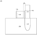
도 11a는 본 개시 내용의 일부 실시예에 따른 반도체 구조체(11A)를 예시한다. 일부 실시예에서, 반도체 구조체(11A)는 트랜지스터의 일부이다. 예를 들어, 반도체 구조체(11A)는 도 9에 도시된 바와 같이 PMOS(901) 또는 NMOS(903)의 일부일 수 있다. 반도체 구조체(11A)는, 기판(110a), 게이트(110b), 게이트 유전체(110c), 스페이서(110d), 콘택(110e), 및 에피택시(110f)를 포함한다.11A illustrates a
도 9의 회로를 참조하면, 에피택시(110f)는 PMOS(901) 또는 NMOS(903)의 소스일 수 있다. 일부 실시예에서, 에피택시(110f)는 PMOS(901) 또는 NMOS(903)의 드레인일 수 있다. 일부 실시예에서, 콘택(110e)은 입력 단자(Vin)에 연결된 PMOS(901)의 소스 콘택일 수 있다. 일부 실시예에서, 콘택(110e)은 출력 단자(Vout)에 연결된 PMOS(901)의 드레인 콘택일 수 있다. 일부 실시예에서, 콘택(110e)은 PMOS(901)의 드레인에 연결된 NMOS(903)의 드레인 콘택일 수있다. 일부 실시예에서, 콘택(110e)은 접지에 연결된 NMOS(903)의 소스 콘택일 수 있다. 게이트(110b)는 다른 입력 단자(Vin1)에 연결된 PMOS(901) 또는 NMOS(903)의 게이트일 수 있다. Referring to the circuit of FIG. 9 , the
게이트 유전체(110c)는 기판(110a) 상에 배치된다. 게이트(110b)는 게이트 유전체(110c) 상에 배치된다. 스페이서(110d)는 기판(110a) 상에 배치된다. 스페이서(110d)는 게이트(110b) 옆에 배치된다. 스페이서(110d)는 게이트(110b) 및 게이트 유전체(110c)와 접촉할 수 있다. 콘택(110e)은 기판(110a) 상에 배치된다. 콘택(110e)은 스페이서(110d) 옆에 배치된다. 콘택(110e)은 스페이서(110d)와 물리적으로 이격되어 있다. 예를 들어, 콘택(110e)과 스페이서(110d) 사이에 갭이 있다. 일부 실시예에서, 콘택(110e)과 게이트(110b) 사이의 거리(D1)는 3 nm 미만이다..A
트랜지스터의 콘택과 게이트 사이의 거리가 3nm 미만이면, 기존 기술을 사용하여 해당 트랜지스터에 대한 전압 스트레스 테스트를 수행하기가 어렵다. 반도체 디바이스의 크기가 점점 작아지므로, 이러한 종류의 구조를 테스트하기가 어렵다. 전압 스트레스 테스트를 수행한 결과의 이스케이프(escape) 결함률은, 본 개시 내용의 방법을 사용함으로써 더 낮아질 것이다. 즉, 본 개시 내용의 방법으로, 콘택과 게이트 사이의 거리가 3nm 미만인 트랜지스터를 테스트하는 것이 더 정확하고 신뢰적일 수 있다. 일부 실시예에서, 도 2a에 도시된 바와 같은 스트레스 신호를 사용하고, 도 9에 도시된 바와 같이 출력 신호를 모니터링함으로써, 전압 스트레스 테스트는 게이트 대 콘택 간격이 3nm 미만인 임의의 트랜지스터에 대해 수행될 수 있다. When the distance between the contact and gate of a transistor is less than 3 nm, it is difficult to perform voltage stress tests on that transistor using conventional techniques. As semiconductor devices become smaller and smaller, it is difficult to test these kinds of structures. The escape defect rate as a result of performing the voltage stress test will be lower by using the method of the present disclosure. That is, with the method of the present disclosure, it may be more accurate and reliable to test transistors with a contact-gate distance of less than 3 nm. In some embodiments, by using a stress signal as shown in Fig. 2A and monitoring the output signal as shown in Fig. 9, a voltage stress test can be performed on any transistor with a gate-to-contact spacing of less than 3 nm. there is.
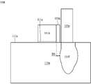
도 11b는 본 개시 내용의 일부 실시예에 따른 반도체 구조물(11B)을 예시한다. 일부 실시예에서, 반도체 구조물(11B)은 트랜지스터의 일부이다. 예를 들어, 반도체 구조물(11B)은 도 9에 도시된 바와 같이 PMOS(901) 또는 NMOS(903)의 일부일 수 있다. 반도체 구조물(11B)은 기판(111a), 게이트(111b), 게이트 유전체(111c), 스페이서(111d), 콘택(111e) 및 에피택시(111f)를 포함한다.11B illustrates a
도 9의 회로를 참조하면, 에피택시(111f)는 PMOS(901) 또는 NMOS(903)의 소스일 수 있다. 일부 실시예에서, 에피택시(111f)는 PMOS(901) 또는 NMOS(903)의 드레인일 수 있다. 일부 실시예에서, 콘택(111e)은 입력 단자(Vin)에 연결된 PMOS(901)의 소스 콘택일 수 있다. 일부 실시예에서, 콘택(111e)은 출력 단자(Vout)에 연결된 PMOS(901)의 드레인 콘택일 수 있다. 일부 실시예에서, 콘택(111e)은 PMOS(901)의 드레인에 연결된 NMOS(903)의 드레인 콘택일 수 있다. 일부 실시예에서, 콘택(111e)은 접지에 연결된 NMOS(903)의 소스 콘택일 수 있다. 게이트(111b)는 다른 입력 단자(Vin1)에 연결된 PMOS(901) 또는 NMOS(903)의 게이트일 수 있다..Referring to the circuit of FIG. 9 , the
기판(111a)은 표면(111s)을 갖는다. 게이트 유전체(111c)는 기판(111a)의 표면(111s) 상에 배치된다. 게이트(111b)는 게이트 유전체(111c) 상에 배치된다. 스페이서(111d)는 기판(111a)의 표면(111s) 상에 배치된다. 스페이서(111d)는 게이트(111b) 옆에 배치된다. 스페이서(111d)는 게이트(111b) 및 게이트 유전체(111c)와 접촉할 수 있다. 콘택(111e)은 기판(111a) 상에 배치된다. 콘택(111e)은 스페이서(111d) 옆에 배치된다. 콘택(111e)은 스페이서(111d)와 물리적으로 이격되어 있다. 예를 들어, 콘택(111e)과 스페이서(111d) 사이에 갭이 있다. 에피택시(111f)는 기판(111a) 내에 배치된다. 에피택시(111f)가 콘택 아래에 있다. 일부 실시예에서, 기판(111a)의 표면(111s) 상의 게이트(111b)의 투사 라인과 기판(111a)의 표면(111s) 상의 에피택시(111f)의 투사 라인 사이의 최소 거리(D2)는 1 nm 미만이다..The
기판 상의 게이트의 투사 라인과 기판 상의 에피택시의 투사 라인 사이의 최소 거리가 1nm 미만이면, 기존 기술을 사용하여 상기 트랜지스터에 대한 전압 스트레스 테스트를 수행하기가 어렵다. 반도체 디바이스의 크기가 점점 작아지므로, 이러한 종류의 구조물을 테스트하기가 어렵다. 기존 기술을 사용하여 전압 스트레스 테스트를 수행한 결과의 이스케이프 결함률은, 본 개시 내용의 방법을 사용함으로써 더 낮아질 것이다. 즉, 본 개시 내용의 방법으로 기판 상의 게이트의 투사 라인과 1 nm 미만의 기판 상의 에피택시의 투사 라인을 갖는 트랜지스터를 테스트하는 것이 더 정확하고 신뢰적일 수 있다. 도 2a에 도시된 바와 같이 스트레스 신호를 사용하고 도 9 및 도 10에 도시된 바와 같이 출력 신호를 모니터링함으로써, 전압 스트레스 테스트는, 게이트 대 에피택시 간격이 1 nm 미만인 임의의 트랜지스터에 대해 수행될 수 있다.If the minimum distance between the projection line of the gate on the substrate and the projection line of the epitaxy on the substrate is less than 1 nm, it is difficult to perform a voltage stress test on the transistor using existing techniques. As semiconductor devices become smaller and smaller, it is difficult to test these kinds of structures. The escape defect rate as a result of performing voltage stress testing using existing techniques will be lower by using the method of the present disclosure. That is, it may be more accurate and reliable to test transistors with projection lines of gates on substrates and projection lines of epitaxy on substrates of less than 1 nm with the methods of the present disclosure. By using a stress signal as shown in Figure 2a and monitoring the output signal as shown in Figures 9 and 10, a voltage stress test can be performed on any transistor with a gate-to-epitaxial spacing of less than 1 nm. there is.
일부 실시예에 따르면, 방법이 제공된다. 이 방법은, 입력 단자 및 출력 단자를 가지는 DUT(Device Under Test)를 제공하는 단계; 제1 기간 동안 상기 DUT의 입력 단자에 제1 전압 레벨을 가지는 전압을 인가하는 단계; 제1 기간 이후의 제2 기간 동안 상기 DUT의 입력 단자에 스트레스 신호를 인가하는 단계; 상기 DUT의 출력 단자에서 상기 스트레스 신호에 응답하여 출력 신호를 획득하는 단계; 및 상기 출력 신호를 상기 스트레스 신호와 비교하는 단계를 포함한다. 상기 스트레스 신호는 복수의 시퀀스를 포함하며, 상기 시퀀스의 각각은 램프-업 스테이지 및 램프-다운 스테이지를 가진다. 상기 스트레스 신호는 제2 전압 레벨 및 제3 전압 레벨을 가진다.According to some embodiments, a method is provided. The method includes providing a device under test (DUT) having an input terminal and an output terminal; applying a voltage having a first voltage level to an input terminal of the DUT for a first period; applying a stress signal to the input terminal of the DUT for a second period after the first period; obtaining an output signal in response to the stress signal at an output terminal of the DUT; and comparing the output signal with the stress signal. The stress signal includes a plurality of sequences, each of which has a ramp-up stage and a ramp-down stage. The stress signal has a second voltage level and a third voltage level.
다른 실시예에 따르면, 방법이 제공된다. 이 방법은, 입력 단자 및 출력 단자를 가지는 DUT를 제공하는 단계; 상기 DUT의 입력 단자에 스트레스 신호를 인가하는 단계; 상기 DUT의 출력 단자에서 상기 스트레스 신호에 응답하여 출력 신호를 획득하는 단계; 상기 출력 신호를 상기 스트레스 신호와 비교하는 단계; 및 상기 출력 신호와 상기 스트레스 신호 간의 비교 결과에 기초하여 상기 DUT가 비정상적인 구조를 갖는지 여부를 결정하는 단계를 포함한다. 상기 출력 신호는 복수의 시퀀스를 포함하며, 상기 시퀀스의 각각은 램프-업 스테이지 및 램프-다운 스테이지를 가진다. 상기 출력 신호는 제1 전압 레벨 및 제2 전압 레벨을 가진다.According to another embodiment, a method is provided. The method includes providing a DUT having an input terminal and an output terminal; applying a stress signal to an input terminal of the DUT; obtaining an output signal in response to the stress signal at an output terminal of the DUT; comparing the output signal with the stress signal; and determining whether the DUT has an abnormal structure based on a comparison result between the output signal and the stress signal. The output signal includes a plurality of sequences, each of which has a ramp-up stage and a ramp-down stage. The output signal has a first voltage level and a second voltage level.
다른 실시예에 따르면, 반도체 디바이스가 제공된다. 반도체 디바이스는, 스트레스 신호를 수신하도록 구성된 제1 입력 단자 및 상기 스트레스 신호에 응답하여 출력 신호를 생성하도록 구성된 출력 단자를 포함한다. 반도체 디바이스는 기판, 게이트, 및 콘택을 더 포함한다. 게이트는 기판 상에 배치된다. 콘택은 기판 상에 그리고 상기 게이트 옆에 배치된다. 콘택은 제1 입력 단자 또는 출력 단자에 전기적으로 연결된다. 게이트와 콘택 사이의 거리는 3 나노미터(nm) 미만이다.According to another embodiment, a semiconductor device is provided. A semiconductor device includes a first input terminal configured to receive a stress signal and an output terminal configured to generate an output signal in response to the stress signal. The semiconductor device further includes a substrate, a gate, and a contact. A gate is disposed on the substrate. A contact is disposed on the substrate and next to the gate. The contact is electrically connected to the first input terminal or the output terminal. The distance between the gate and the contact is less than 3 nanometers (nm).
전술한 내용은, 기술 분야의 숙련된 자가 본 개시의 양태를 더 잘 이해할 수도 있도록 여러 가지 실시형태의 피처를 개략적으로 나타낸다. 기술 분야의 숙련된 자는, 그들이 동일한 목적을 실행하기 위해 및/또는 본원에서 소개되는 실시형태의 동일한 이점을 달성하기 위해 다른 프로세스 및 구조물을 설계 또는 수정하기 위한 기초로서 본 개시를 쉽게 사용할 수도 있다는 것을 인식해야 한다. 기술 분야의 숙련된 자는 또한, 그러한 등가적 구성이 본 개시의 취지와 범위를 벗어나지 않는다는 것, 및 그들이 본 개시의 취지와 범위를 벗어나지 않으면서 본원에서 다양한 변경, 대체, 수정을 가할 수도 있다는 것을 인식해야 한다.The foregoing outlines features of various embodiments so that those skilled in the art may better understand aspects of the present disclosure. Those skilled in the art will recognize that they may readily use the present disclosure as a basis for designing or modifying other processes and structures for carrying out the same purposes and/or achieving the same advantages of the embodiments introduced herein. have to recognize Those skilled in the art will also recognize that such equivalent constructions do not depart from the spirit and scope of the present disclosure, and that they may make various changes, substitutions, and modifications herein without departing from the spirit and scope of the present disclosure. Should be.
<부 기><Note>
1. 방법에 있어서,1. A method comprising:
입력 단자 및 출력 단자를 가지는 DUT(Device Under Test)를 제공하는 단계;providing a device under test (DUT) having an input terminal and an output terminal;
제1 기간 동안 상기 DUT의 입력 단자에 제1 전압 레벨을 가지는 전압을 인가하는 단계;applying a voltage having a first voltage level to an input terminal of the DUT for a first period;
제1 기간 이후의 제2 기간 동안 상기 DUT의 입력 단자에 스트레스(stress) 신호를 인가하는 단계 - 상기 스트레스 신호는 복수의 시퀀스를 포함하며, 상기 시퀀스의 각각은 램프-업(ramp-up) 스테이지 및 램프-다운(ramp-down) 스테이지를 가지며, 상기 스트레스 신호는 제2 전압 레벨 및 제3 전압 레벨을 가짐 -;applying a stress signal to the input terminal of the DUT for a second period after the first period, the stress signal comprising a plurality of sequences, each of the sequences being subjected to a ramp-up stage and a ramp-down stage, wherein the stress signal has a second voltage level and a third voltage level;
상기 DUT의 출력 단자에서 상기 스트레스 신호에 응답하여 출력 신호를 획득하는 단계; 및obtaining an output signal in response to the stress signal at an output terminal of the DUT; and
상기 출력 신호를 상기 스트레스 신호와 비교하는 단계comparing the output signal with the stress signal
를 포함하는 방법.How to include.
2. 제1항에 있어서, 상기 출력 신호와 상기 스트레스 신호 간의 비교 결과에 기초하여 상기 DUT가 비정상적인(abnormal) 구조를 갖는지 여부를 결정하는 단계를 더 포함하는 방법.2. The method according to
3. 제2항에 있어서, 상기 DUT는 동일한 시간 영역에서 상기 출력 신호가 상기 스트레스 신호와 논리적으로 상이한 경우에 비정상적인 구조를 갖는 것으로 결정되는 것인 방법.3. The method according to clause 2, wherein the DUT is determined to have an abnormal structure when the output signal is logically different from the stress signal in the same time domain.
4. 제3항에 있어서, 상기 출력 신호는 상기 동일한 시간 영역에서 부분적으로 상기 스트레스 신호와 논리적으로 상이한 것인 방법.4. The method of clause 3, wherein the output signal is logically different from the stress signal in part in the same time domain.
5. 제3항에 있어서, 상기 출력 신호는 상기 동일한 시간 영역에서 완전히(fully) 상기 스트레스 신호와 논리적으로 상이한 것인 방법.5. The method of clause 3, wherein the output signal is logically different from the stress signal fully in the same time domain.
6. 제1항에 있어서, 상기 제2 전압 레벨은 상기 제1 전압 레벨보다 1.3 배 내지 3.0 배 더 높은 것인 방법.6. The method of
7. 제1항에 있어서, 상기 제3 전압 레벨은 상기 제1 전압 레벨의 0.7 배 내지 상기 제2 전압 레벨의 0.9 배인 것인 방법.7. The method of
8. 제1항에 있어서, 상기 DUT는,8. The method of 1, wherein the DUT comprises:
상기 DUT의 입력 단자에 연결되는 소스, 게이트, 및 상기 DUT의 출력 단자에 연결되는 드레인을 가지는 PMOS; 및a PMOS having a source coupled to an input terminal of the DUT, a gate, and a drain coupled to an output terminal of the DUT; and
접지에 연결되는 소스, 상기 PMOS의 상기 게이트에 연결되는 게이트, 및 상기 DUT의 출력 단자에 연결되는 드레인을 가지는 NMOS NMOS having a source coupled to ground, a gate coupled to the gate of the PMOS, and a drain coupled to the output terminal of the DUT
를 포함하는 방법.How to include.
9. 방법에 있어서,9. A method comprising:
입력 단자 및 출력 단자를 가지는 DUT를 제공하는 단계;providing a DUT having an input terminal and an output terminal;
상기 DUT의 입력 단자에 스트레스 신호를 인가하는 단계;applying a stress signal to an input terminal of the DUT;
상기 DUT의 출력 단자에서 상기 스트레스 신호에 응답하여 출력 신호를 획득하는 단계 - 상기 출력 신호는 복수의 시퀀스를 포함하며, 상기 시퀀스의 각각은 램프-업 스테이지 및 램프-다운 스테이지를 가지며, 상기 출력 신호는 제1 전압 레벨 및 제2 전압 레벨을 가짐 -;obtaining an output signal in response to the stress signal at an output terminal of the DUT, the output signal comprising a plurality of sequences, each of the sequences having a ramp-up stage and a ramp-down stage, the output signal has a first voltage level and a second voltage level;
상기 출력 신호를 상기 스트레스 신호와 비교하는 단계; 및comparing the output signal with the stress signal; and
상기 출력 신호와 상기 스트레스 신호 간의 비교 결과에 기초하여 상기 DUT가 비정상적인 구조를 갖는지 여부를 결정하는 단계determining whether the DUT has an abnormal structure based on a comparison result between the output signal and the stress signal;
를 포함하는 방법.How to include.
10. 제9항에 있어서, 상기 스트레스 신호를 인가하기 전에 상기 DUT의 입력 단자에 제3 전압 레벨을 갖는 전압을 인가하는 단계를 더 포함하는 방법.10. The method of clause 9, further comprising applying a voltage having a third voltage level to an input terminal of the DUT prior to applying the stress signal.
11. 제10항에 있어서, 상기 제1 전압 레벨은 상기 제3 전압 레벨보다 약 1.3 배 내지 약 3.0 배 더 높은 것인 방법.11. The method of clause 10, wherein the first voltage level is from about 1.3 times to about 3.0 times higher than the third voltage level.
12. 제10항에 있어서, 상기 제2 전압 레벨은 상기 제3 전압 레벨의 약 0.7 배 내지 상기 제1 전압 레벨의 약 0.9 배인 것인 방법.12. The method of clause 10, wherein the second voltage level is between about 0.7 times the third voltage level and about 0.9 times the first voltage level.
13. 제9항에 있어서, 상기 DUT는 동일한 시간 영역에서 상기 출력 신호가 상기 스트레스 신호와 논리적으로 상이한 경우에 비정상인 구조를 갖는 것으로서 결정되는 것인 방법.13. The method of clause 9, wherein the DUT is determined as having an anomalous structure when the output signal is logically different from the stress signal in the same time domain.
14. 제9항에 있어서, 상기 DUT는,14. The method of claim 9, wherein the DUT comprises:
상기 DUT의 입력 단자에 연결되는 소스, 게이트, 및 상기 DUT의 출력 단자에 연결되는 드레인을 가지는 PMOS; 및a PMOS having a source coupled to an input terminal of the DUT, a gate, and a drain coupled to an output terminal of the DUT; and
접지에 연결되는 소스, 상기 PMOS의 상기 게이트에 연결되는 게이트, 및 상기 DUT의 출력 단자에 연결되는 드레인을 가지는 NMOSNMOS having a source coupled to ground, a gate coupled to the gate of the PMOS, and a drain coupled to the output terminal of the DUT
를 포함하는 방법.How to include.
15. 반도체 디바이스로서,15. A semiconductor device comprising:
스트레스 신호를 수신하도록 구성된 제1 입력 단자;a first input terminal configured to receive a stress signal;
상기 스트레스 신호에 응답하여 출력 신호를 생성하도록 구성된 출력 단자;an output terminal configured to generate an output signal in response to the stress signal;
기판;Board;
상기 기판 상에 배치된 게이트; 및a gate disposed on the substrate; and
상기 기판 상에 그리고 상기 게이트 옆에 배치된 콘택 - 상기 콘택은 상기 제1 입력 단자 또는 상기 출력 단자에 전기적으로 연결되고, 상기 게이트와 상기 콘택 사이의 거리가 3 나노미터(nm) 미만임 -a contact disposed on the substrate and next to the gate, the contact electrically connected to the first input terminal or the output terminal, and wherein a distance between the gate and the contact is less than 3 nanometers (nm);
을 포함하는 반도체 디바이스.A semiconductor device comprising a.
16. 제15항에 있어서, 상기 기판 내에 그리고 상기 콘택 아래에 배치된 에피택시를 더 포함하고, 상기 기판 상의 게이트의 투사(projection) 라인과 상기 기판 상의 에피택시의 투사 라인 사이의 최소 거리는 1 nm 미만인 반도체 디바이스.16. The method of clause 15, further comprising an epitaxy disposed in the substrate and below the contact, wherein a minimum distance between a projection line of a gate on the substrate and a projection line of the epitaxy on the substrate is 1 nm less than a semiconductor device.
17. 제15항에 있어서, 17. Clause 15,
상기 기판 상에 그리고 상기 게이트와 상기 콘택 사이에 배치된 스페이서; 및a spacer disposed on the substrate and between the gate and the contact; and
상기 게이트와 상기 기판 사이에 배치된 게이트 유전체a gate dielectric disposed between the gate and the substrate
를 더 포함하는 반도체 디바이스.A semiconductor device further comprising a.
18. 제15항에 있어서, 상기 스트레스 신호에 응답하는 상기 출력 신호는 복수의 시퀀스를 포함하고, 상기 시퀀스의 각각은 램프-업 스테이지 및 램프-다운 스테이지를 가지며, 상기 출력 신호는 제1 전압 레벨 및 제2 전압 레벨을 가지는 것인 반도체 디바이스.18. The method of clause 15, wherein the output signal responsive to the stress signal comprises a plurality of sequences, each of the sequences having a ramp-up stage and a ramp-down stage, the output signal having a first voltage level and a second voltage level.
19. 제18항에 있어서, 상기 반도체 디바이스의 상기 제1 입력 단자는 또한, 상기 스트레스 신호를 수신하기 전에 제3 전압 레벨을 가지는 전압을 수신하도록 구성되는 것인 반도체 디바이스.19. The semiconductor device of claim 18, wherein the first input terminal of the semiconductor device is further configured to receive a voltage having a third voltage level prior to receiving the stress signal.
20. 제19항에 있어서, 상기 콘택은 상기 반도체 디바이스의 드레인 또는 소스에 전기적으로 연결되는 것인 반도체 디바이스.20. The semiconductor device of clause 19, wherein the contact is electrically connected to a drain or source of the semiconductor device.
Claims (10)
입력 단자 및 출력 단자를 가지는 DUT(Device Under Test)를 제공하는 단계;
제1 기간 동안 상기 DUT의 입력 단자에 제1 전압 레벨을 가지는 전압을 인가하는 단계;
제1 기간 이후의 제2 기간 동안 상기 DUT의 입력 단자에 스트레스(stress) 신호를 인가하는 단계 - 상기 스트레스 신호는 복수의 시퀀스를 포함하며, 상기 시퀀스의 각각은 램프-업(ramp-up) 스테이지 및 램프-다운(ramp-down) 스테이지를 가지며, 상기 스트레스 신호는 제2 전압 레벨 및 제3 전압 레벨을 가짐 -;
상기 DUT의 출력 단자에서 상기 스트레스 신호에 응답하여 출력 신호를 획득하는 단계; 및
상기 출력 신호를 상기 스트레스 신호와 비교하는 단계
를 포함하는 방법.In the method,
providing a device under test (DUT) having an input terminal and an output terminal;
applying a voltage having a first voltage level to an input terminal of the DUT for a first period;
applying a stress signal to the input terminal of the DUT for a second period after the first period, the stress signal comprising a plurality of sequences, each of the sequences being subjected to a ramp-up stage and a ramp-down stage, wherein the stress signal has a second voltage level and a third voltage level;
obtaining an output signal in response to the stress signal at an output terminal of the DUT; and
comparing the output signal with the stress signal
How to include.
상기 DUT의 입력 단자에 연결되는 소스, 게이트, 및 상기 DUT의 출력 단자에 연결되는 드레인을 가지는 PMOS; 및
접지에 연결되는 소스, 상기 PMOS의 상기 게이트에 연결되는 게이트, 및 상기 DUT의 출력 단자에 연결되는 드레인을 가지는 NMOS
를 포함하는 방법.The method of claim 1, wherein the DUT comprises:
a PMOS having a source coupled to an input terminal of the DUT, a gate, and a drain coupled to an output terminal of the DUT; and
NMOS having a source coupled to ground, a gate coupled to the gate of the PMOS, and a drain coupled to the output terminal of the DUT
How to include.
입력 단자 및 출력 단자를 가지는 DUT를 제공하는 단계;
상기 DUT의 입력 단자에 스트레스 신호를 인가하는 단계;
상기 DUT의 출력 단자에서 상기 스트레스 신호에 응답하여 출력 신호를 획득하는 단계 - 상기 출력 신호는 복수의 시퀀스를 포함하며, 상기 시퀀스의 각각은 램프-업 스테이지 및 램프-다운 스테이지를 가지며, 상기 출력 신호는 제1 전압 레벨 및 제2 전압 레벨을 가짐 -;
상기 출력 신호를 상기 스트레스 신호와 비교하는 단계; 및
상기 출력 신호와 상기 스트레스 신호 간의 비교 결과에 기초하여 상기 DUT가 비정상적인 구조를 갖는지 여부를 결정하는 단계
를 포함하는 방법.In the method,
providing a DUT having an input terminal and an output terminal;
applying a stress signal to an input terminal of the DUT;
obtaining an output signal in response to the stress signal at an output terminal of the DUT, the output signal comprising a plurality of sequences, each of the sequences having a ramp-up stage and a ramp-down stage, the output signal has a first voltage level and a second voltage level;
comparing the output signal with the stress signal; and
determining whether the DUT has an abnormal structure based on a comparison result between the output signal and the stress signal;
How to include.
스트레스 신호를 수신하도록 구성된 제1 입력 단자;
상기 스트레스 신호에 응답하여 출력 신호를 생성하도록 구성된 출력 단자;
기판;
상기 기판 상에 배치된 게이트; 및
상기 기판 상에 그리고 상기 게이트 옆에 배치된 콘택 - 상기 콘택은 상기 제1 입력 단자 또는 상기 출력 단자에 전기적으로 연결되고, 상기 게이트와 상기 콘택 사이의 거리가 3 나노미터(nm) 미만임 -
을 포함하는 반도체 디바이스.A semiconductor device comprising:
a first input terminal configured to receive a stress signal;
an output terminal configured to generate an output signal in response to the stress signal;
Board;
a gate disposed on the substrate; and
a contact disposed on the substrate and next to the gate, the contact electrically connected to the first input terminal or the output terminal, and wherein a distance between the gate and the contact is less than 3 nanometers (nm);
A semiconductor device comprising a.
상기 기판 상에 그리고 상기 게이트와 상기 콘택 사이에 배치된 스페이서; 및
상기 게이트와 상기 기판 사이에 배치된 게이트 유전체
를 더 포함하는 반도체 디바이스.7. The method of claim 6,
a spacer disposed on the substrate and between the gate and the contact; and
a gate dielectric disposed between the gate and the substrate
A semiconductor device further comprising a.
Applications Claiming Priority (6)
| Application Number | Priority Date | Filing Date | Title |
|---|---|---|---|
| US202063092743P | 2020-10-16 | 2020-10-16 | |
| US63/092,743 | 2020-10-16 | ||
| US202063115280P | 2020-11-18 | 2020-11-18 | |
| US63/115,280 | 2020-11-18 | ||
| US17/198,764 | 2021-03-11 | ||
| US17/198,764 US11448692B2 (en) | 2018-08-16 | 2021-03-11 | Method and device for wafer-level testing |
Publications (2)
| Publication Number | Publication Date |
|---|---|
| KR20220050737A true KR20220050737A (en) | 2022-04-25 |
| KR102590203B1 KR102590203B1 (en) | 2023-10-16 |
Family
ID=80929234
Family Applications (1)
| Application Number | Title | Priority Date | Filing Date |
|---|---|---|---|
| KR1020210061308A Active KR102590203B1 (en) | 2020-10-16 | 2021-05-12 | Method and device for wafer-level testing |
Country Status (4)
| Country | Link |
|---|---|
| KR (1) | KR102590203B1 (en) |
| CN (1) | CN114373691A (en) |
| DE (1) | DE102021106795A1 (en) |
| TW (1) | TWI775435B (en) |
Families Citing this family (1)
| Publication number | Priority date | Publication date | Assignee | Title |
|---|---|---|---|---|
| CN111983421B (en) * | 2019-05-24 | 2023-07-25 | 台湾积体电路制造股份有限公司 | Circuit detection system and circuit detection method |
Citations (12)
| Publication number | Priority date | Publication date | Assignee | Title |
|---|---|---|---|---|
| EP0348099A2 (en) * | 1988-06-21 | 1989-12-27 | AT&T Corp. | Floating gate memories |
| KR20000026475A (en) * | 1998-10-20 | 2000-05-15 | 윤종용 | Test circuit with power on reset circuit |
| KR20030089021A (en) * | 2002-05-15 | 2003-11-21 | 삼성전자주식회사 | Integrated circuit chip having test element group circuit and method of making the same |
| US20060234398A1 (en) * | 2005-04-15 | 2006-10-19 | International Business Machines Corporation | Single ic-chip design on wafer with an embedded sensor utilizing rf capabilities to enable real-time data transmission |
| US20090167339A1 (en) * | 2007-12-31 | 2009-07-02 | Andrew Marshall | Contactless Testing of Wafer Characteristics |
| US20100182859A1 (en) * | 2007-10-29 | 2010-07-22 | Kohler Ross A | Method and Apparatus for Testing a Memory Device |
| US20110037494A1 (en) * | 2009-08-11 | 2011-02-17 | Taiwan Semiconductor Manufacturing Company, Ltd. | Method for Wafer-Level Testing of Integrated Circuits |
| KR20110021892A (en) * | 2008-05-15 | 2011-03-04 | 퀄컴 인코포레이티드 | Testing of Memory Devices with Field Effect Transistors Experiencing Threshold Voltage Shifts Caused by Bias Temperature Instability |
| KR20140031075A (en) * | 2012-09-04 | 2014-03-12 | 타이완 세미콘덕터 매뉴팩쳐링 컴퍼니 리미티드 | Qualitative fault detection and classification system for tool condition monitoring and associated methods |
| KR20150073460A (en) * | 2013-12-23 | 2015-07-01 | 엘지디스플레이 주식회사 | Test apparatus for display device |
| US9176167B1 (en) * | 2011-08-21 | 2015-11-03 | Bruker Nano Inc. | Probe and method of manufacture for semiconductor wafer characterization |
| US20170350938A1 (en) * | 2016-06-01 | 2017-12-07 | Taiwan Semiconductor Manufacturing Co., Ltd. | Ic degradation management circuit, system and method |
Family Cites Families (6)
| Publication number | Priority date | Publication date | Assignee | Title |
|---|---|---|---|---|
| US4853561A (en) * | 1987-06-10 | 1989-08-01 | Regents Of The University Of Minnesota | Family of noise-immune logic gates and memory cells |
| JPH07288463A (en) * | 1994-04-18 | 1995-10-31 | Nec Corp | Bicmos semiconductor integrated circuit |
| JP3391249B2 (en) * | 1998-03-11 | 2003-03-31 | ヤマハ株式会社 | Analog signal delay circuit |
| JP4951907B2 (en) * | 2005-09-16 | 2012-06-13 | 富士電機株式会社 | Semiconductor circuit, inverter circuit, and semiconductor device |
| WO2018190881A1 (en) * | 2017-04-15 | 2018-10-18 | Intel IP Corporation | Multi-drain esd-robust transistor arrangements |
| US11073551B2 (en) * | 2018-08-16 | 2021-07-27 | Taiwan Semiconductor Manufacturing Company Ltd. | Method and system for wafer-level testing |
-
2021
- 2021-03-19 DE DE102021106795.2A patent/DE102021106795A1/en active Pending
- 2021-05-12 KR KR1020210061308A patent/KR102590203B1/en active Active
- 2021-05-14 TW TW110117581A patent/TWI775435B/en active
- 2021-06-25 CN CN202110710654.3A patent/CN114373691A/en active Pending
Patent Citations (13)
| Publication number | Priority date | Publication date | Assignee | Title |
|---|---|---|---|---|
| EP0348099A2 (en) * | 1988-06-21 | 1989-12-27 | AT&T Corp. | Floating gate memories |
| EP0348099B1 (en) * | 1988-06-21 | 1994-08-31 | AT&T Corp. | Floating gate memories |
| KR20000026475A (en) * | 1998-10-20 | 2000-05-15 | 윤종용 | Test circuit with power on reset circuit |
| KR20030089021A (en) * | 2002-05-15 | 2003-11-21 | 삼성전자주식회사 | Integrated circuit chip having test element group circuit and method of making the same |
| US20060234398A1 (en) * | 2005-04-15 | 2006-10-19 | International Business Machines Corporation | Single ic-chip design on wafer with an embedded sensor utilizing rf capabilities to enable real-time data transmission |
| US20100182859A1 (en) * | 2007-10-29 | 2010-07-22 | Kohler Ross A | Method and Apparatus for Testing a Memory Device |
| US20090167339A1 (en) * | 2007-12-31 | 2009-07-02 | Andrew Marshall | Contactless Testing of Wafer Characteristics |
| KR20110021892A (en) * | 2008-05-15 | 2011-03-04 | 퀄컴 인코포레이티드 | Testing of Memory Devices with Field Effect Transistors Experiencing Threshold Voltage Shifts Caused by Bias Temperature Instability |
| US20110037494A1 (en) * | 2009-08-11 | 2011-02-17 | Taiwan Semiconductor Manufacturing Company, Ltd. | Method for Wafer-Level Testing of Integrated Circuits |
| US9176167B1 (en) * | 2011-08-21 | 2015-11-03 | Bruker Nano Inc. | Probe and method of manufacture for semiconductor wafer characterization |
| KR20140031075A (en) * | 2012-09-04 | 2014-03-12 | 타이완 세미콘덕터 매뉴팩쳐링 컴퍼니 리미티드 | Qualitative fault detection and classification system for tool condition monitoring and associated methods |
| KR20150073460A (en) * | 2013-12-23 | 2015-07-01 | 엘지디스플레이 주식회사 | Test apparatus for display device |
| US20170350938A1 (en) * | 2016-06-01 | 2017-12-07 | Taiwan Semiconductor Manufacturing Co., Ltd. | Ic degradation management circuit, system and method |
Also Published As
| Publication number | Publication date |
|---|---|
| TW202217996A (en) | 2022-05-01 |
| TWI775435B (en) | 2022-08-21 |
| DE102021106795A1 (en) | 2022-04-21 |
| CN114373691A (en) | 2022-04-19 |
| KR102590203B1 (en) | 2023-10-16 |
Similar Documents
| Publication | Publication Date | Title |
|---|---|---|
| US12066484B2 (en) | Method and device for wafer-level testing | |
| US6815971B2 (en) | Method and apparatus for stress testing integrated circuits using an adjustable AC hot carrier injection source | |
| US12025655B2 (en) | Method and system for wafer-level testing | |
| KR100466984B1 (en) | Integrated circuit chip having test element group circuit and method of test the same | |
| US8004297B2 (en) | Isolation circuit | |
| US11573261B2 (en) | Semiconductor device and method of operating the same | |
| KR102590203B1 (en) | Method and device for wafer-level testing | |
| US6950355B2 (en) | System and method to screen defect related reliability failures in CMOS SRAMS | |
| KR100576492B1 (en) | Internal DC Bias Measurement Device for Semiconductor Devices at Package Level | |
| US20250383394A1 (en) | Time-dependent dielectric breakdown (tddb) test unit, measurement circuit and method thereof | |
| US12044723B2 (en) | Circuit for temperature stress test for memory chips | |
| JP2954076B2 (en) | Semiconductor integrated circuit wafer and test method therefor | |
| KR100934793B1 (en) | Semiconductor device test method and apparatus and proper stress voltage detection method | |
| Sim et al. | A case study on different test screening techniques for ICS with high resistance vias interconnects issues | |
| KR20080088676A (en) | Test device of semiconductor device |
Legal Events
| Date | Code | Title | Description |
|---|---|---|---|
| PA0109 | Patent application |
Patent event code: PA01091R01D Comment text: Patent Application Patent event date: 20210512 |
|
| PA0201 | Request for examination | ||
| PG1501 | Laying open of application | ||
| E902 | Notification of reason for refusal | ||
| PE0902 | Notice of grounds for rejection |
Comment text: Notification of reason for refusal Patent event date: 20230215 Patent event code: PE09021S01D |
|
| E701 | Decision to grant or registration of patent right | ||
| PE0701 | Decision of registration |
Patent event code: PE07011S01D Comment text: Decision to Grant Registration Patent event date: 20230718 |
|
| GRNT | Written decision to grant | ||
| PR0701 | Registration of establishment |
Comment text: Registration of Establishment Patent event date: 20231012 Patent event code: PR07011E01D |
|
| PR1002 | Payment of registration fee |
Payment date: 20231012 End annual number: 3 Start annual number: 1 |
|
| PG1601 | Publication of registration |