KR20180098757A - 수직형 메모리 장치 - Google Patents
수직형 메모리 장치 Download PDFInfo
- Publication number
- KR20180098757A KR20180098757A KR1020170025279A KR20170025279A KR20180098757A KR 20180098757 A KR20180098757 A KR 20180098757A KR 1020170025279 A KR1020170025279 A KR 1020170025279A KR 20170025279 A KR20170025279 A KR 20170025279A KR 20180098757 A KR20180098757 A KR 20180098757A
- Authority
- KR
- South Korea
- Prior art keywords
- gate
- pattern
- gate electrode
- substrate
- region
- Prior art date
- Legal status (The legal status is an assumption and is not a legal conclusion. Google has not performed a legal analysis and makes no representation as to the accuracy of the status listed.)
- Granted
Links
Images


Classifications
-
- H—ELECTRICITY
- H10—SEMICONDUCTOR DEVICES; ELECTRIC SOLID-STATE DEVICES NOT OTHERWISE PROVIDED FOR
- H10B—ELECTRONIC MEMORY DEVICES
- H10B43/00—EEPROM devices comprising charge-trapping gate insulators
- H10B43/20—EEPROM devices comprising charge-trapping gate insulators characterised by three-dimensional arrangements, e.g. with cells on different height levels
- H10B43/23—EEPROM devices comprising charge-trapping gate insulators characterised by three-dimensional arrangements, e.g. with cells on different height levels with source and drain on different levels, e.g. with sloping channels
- H10B43/27—EEPROM devices comprising charge-trapping gate insulators characterised by three-dimensional arrangements, e.g. with cells on different height levels with source and drain on different levels, e.g. with sloping channels the channels comprising vertical portions, e.g. U-shaped channels
-
- H—ELECTRICITY
- H10—SEMICONDUCTOR DEVICES; ELECTRIC SOLID-STATE DEVICES NOT OTHERWISE PROVIDED FOR
- H10B—ELECTRONIC MEMORY DEVICES
- H10B41/00—Electrically erasable-and-programmable ROM [EEPROM] devices comprising floating gates
-
- H01L27/11582—
-
- H—ELECTRICITY
- H10—SEMICONDUCTOR DEVICES; ELECTRIC SOLID-STATE DEVICES NOT OTHERWISE PROVIDED FOR
- H10B—ELECTRONIC MEMORY DEVICES
- H10B41/00—Electrically erasable-and-programmable ROM [EEPROM] devices comprising floating gates
- H10B41/20—Electrically erasable-and-programmable ROM [EEPROM] devices comprising floating gates characterised by three-dimensional arrangements, e.g. with cells on different height levels
- H10B41/23—Electrically erasable-and-programmable ROM [EEPROM] devices comprising floating gates characterised by three-dimensional arrangements, e.g. with cells on different height levels with source and drain on different levels, e.g. with sloping channels
- H10B41/27—Electrically erasable-and-programmable ROM [EEPROM] devices comprising floating gates characterised by three-dimensional arrangements, e.g. with cells on different height levels with source and drain on different levels, e.g. with sloping channels the channels comprising vertical portions, e.g. U-shaped channels
-
- H01L27/11573—
-
- H01L29/66628—
-
- H01L29/7834—
-
- H01L29/7926—
-
- H—ELECTRICITY
- H10—SEMICONDUCTOR DEVICES; ELECTRIC SOLID-STATE DEVICES NOT OTHERWISE PROVIDED FOR
- H10B—ELECTRONIC MEMORY DEVICES
- H10B43/00—EEPROM devices comprising charge-trapping gate insulators
-
- H—ELECTRICITY
- H10—SEMICONDUCTOR DEVICES; ELECTRIC SOLID-STATE DEVICES NOT OTHERWISE PROVIDED FOR
- H10B—ELECTRONIC MEMORY DEVICES
- H10B43/00—EEPROM devices comprising charge-trapping gate insulators
- H10B43/30—EEPROM devices comprising charge-trapping gate insulators characterised by the memory core region
-
- H—ELECTRICITY
- H10—SEMICONDUCTOR DEVICES; ELECTRIC SOLID-STATE DEVICES NOT OTHERWISE PROVIDED FOR
- H10B—ELECTRONIC MEMORY DEVICES
- H10B43/00—EEPROM devices comprising charge-trapping gate insulators
- H10B43/40—EEPROM devices comprising charge-trapping gate insulators characterised by the peripheral circuit region
-
- H—ELECTRICITY
- H10—SEMICONDUCTOR DEVICES; ELECTRIC SOLID-STATE DEVICES NOT OTHERWISE PROVIDED FOR
- H10B—ELECTRONIC MEMORY DEVICES
- H10B43/00—EEPROM devices comprising charge-trapping gate insulators
- H10B43/50—EEPROM devices comprising charge-trapping gate insulators characterised by the boundary region between the core and peripheral circuit regions
-
- H—ELECTRICITY
- H10—SEMICONDUCTOR DEVICES; ELECTRIC SOLID-STATE DEVICES NOT OTHERWISE PROVIDED FOR
- H10D—INORGANIC ELECTRIC SEMICONDUCTOR DEVICES
- H10D30/00—Field-effect transistors [FET]
- H10D30/01—Manufacture or treatment
- H10D30/021—Manufacture or treatment of FETs having insulated gates [IGFET]
- H10D30/027—Manufacture or treatment of FETs having insulated gates [IGFET] of lateral single-gate IGFETs
- H10D30/0275—Manufacture or treatment of FETs having insulated gates [IGFET] of lateral single-gate IGFETs forming single crystalline semiconductor source or drain regions resulting in recessed gates, e.g. forming raised source or drain regions
-
- H—ELECTRICITY
- H10—SEMICONDUCTOR DEVICES; ELECTRIC SOLID-STATE DEVICES NOT OTHERWISE PROVIDED FOR
- H10D—INORGANIC ELECTRIC SEMICONDUCTOR DEVICES
- H10D30/00—Field-effect transistors [FET]
- H10D30/60—Insulated-gate field-effect transistors [IGFET]
- H10D30/601—Insulated-gate field-effect transistors [IGFET] having lightly-doped drain or source extensions, e.g. LDD IGFETs or DDD IGFETs
- H10D30/608—Insulated-gate field-effect transistors [IGFET] having lightly-doped drain or source extensions, e.g. LDD IGFETs or DDD IGFETs having non-planar bodies, e.g. having recessed gate electrodes
-
- H—ELECTRICITY
- H10—SEMICONDUCTOR DEVICES; ELECTRIC SOLID-STATE DEVICES NOT OTHERWISE PROVIDED FOR
- H10D—INORGANIC ELECTRIC SEMICONDUCTOR DEVICES
- H10D30/00—Field-effect transistors [FET]
- H10D30/60—Insulated-gate field-effect transistors [IGFET]
- H10D30/69—IGFETs having charge trapping gate insulators, e.g. MNOS transistors
- H10D30/693—Vertical IGFETs having charge trapping gate insulators
Landscapes
- Non-Volatile Memory (AREA)
- Semiconductor Memories (AREA)
- Chemical & Material Sciences (AREA)
- Crystallography & Structural Chemistry (AREA)
Abstract
Description
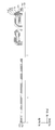
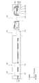
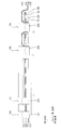
도 11 내지 도 14는 예시적인 실시예들에 따른 수직형 메모리 장치의 제조 방법의 단계들을 설명하기 위한 단면도들이다.
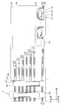
120, 125: 제1, 제2 폴리실리콘 패턴
130, 135: 제1, 제2 금속 패턴 140, 145: 제1, 제2 게이트 마스크
150: 게이트 스페이서
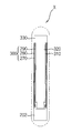
162, 164, 215, 115: 제1 내지 제4 절연 패턴
172, 225: 제1, 제2 희생 패턴
180: 제1 층간 절연막 192, 194: 제1, 제2 개구
202, 204: 제1, 제2 에피택시얼 층
210: 제2 절연막 220: 희생막
230: 제3 층간 절연 패턴
240, 340, 440, 460: 제4 내지 제7 층간 절연막
250: 채널 홀 270: 제1 블로킹 패턴
280: 전하 저장 패턴 290: 터널 절연 패턴
300: 전하 저장 구조물 310: 채널
320: 충전 패턴 330: 캐핑 패턴
370: 제2 블로킹 막
383, 385, 387: 제1 내지 제3 게이트 배리어 패턴
393, 395, 397: 제1 내지 제3 게이트 도전 패턴
403, 405, 407: 제2 내지 제4 게이트 전극
452, 454, 456, 458: 제1 내지 제4 콘택
472, 474, 476, 478: 제1 내지 제4 배선
Claims (10)
- 셀 영역 및 주변 회로 영역을 포함하는 기판의 상기 주변 회로 영역 상에 형성되어 제1 게이트 전극을 포함하는 게이트 구조물;
상기 기판 상면에 수직한 수직 방향을 따라 상기 기판의 셀 영역 상의 복수의 층들에 순차적으로 형성된 제2 내지 제4 게이트 전극들;
상기 기판의 셀 영역 상에 형성되어 상기 제2 게이트 전극을 관통하는 제1 에피택시얼 층;
상기 제1 에피택시얼 층 상에 상기 수직 방향을 따라 연장되어 상기 제3 및 제4 게이트 전극들을 관통하는 채널; 및
상기 게이트 구조물에 인접한 상기 기판의 주변 회로 영역 상에 형성된 제2 에피택시얼 층을 포함하는 수직형 메모리 장치. - 제1항에 있어서, 상기 제1 및 제2 에피택시얼 층들은 서로 동일한 물질을 포함하는 수직형 메모리 장치.
- 제1항에 있어서, 상기 게이트 구조물의 표면 상에 형성되어 질화물을 포함하는 식각 저지 패턴을 더 포함하며,
상기 식각 저지 패턴의 두께는 상기 제2 게이트 전극의 두께보다 큰 수직형 메모리 장치. - 제3항에 있어서, 상기 제2 게이트 전극의 적어도 상하면을 커버하는 블로킹 패턴을 더 포함하며,
상기 식각 저지 패턴의 두께는 상기 제2 게이트 전극의 두께, 및 상기 제2 게이트 전극 상하면을 커버하는 상기 블로킹 패턴의 두께의 합과 실질적으로 동일한 수직형 메모리 장치. - 제1항에 있어서, 상기 게이트 구조물은 순차적으로 적층된 게이트 절연 패턴, 상기 제1 게이트 전극, 및 게이트 마스크를 포함하며,
상기 제1 게이트 전극은 순차적으로 적층된 제1 폴리실리콘 패턴 및 제1 금속 패턴을 포함하는 수직형 메모리 장치. - 제5항에 있어서, 상기 제2 게이트 전극은 순차적으로 적층된 제2 폴리실리콘 패턴 및 제2 금속 패턴을 포함하며,
상기 제1 및 제2 금속 패턴들은 서로 동일한 금속을 포함하는 수직형 메모리 장치. - 제6항에 있어서, 상기 제1 및 제2 폴리실리콘 패턴들은 서로 동일한 두께를 가지며, 상기 제1 및 제2 금속 패턴들은 서로 동일한 두께를 갖는 수직형 메모리 장치.
- 셀 영역 및 주변 회로 영역을 포함하는 기판의 상기 주변 회로 영역 상에 형성되어 제1 게이트 전극을 포함하는 게이트 구조물;
상기 게이트 구조물에 인접한 상기 기판의 주변 회로 영역 상에 형성된 소스/드레인 층;
상기 기판 상면에 수직한 수직 방향을 따라 상기 기판의 셀 영역 상의 복수의 층들에 순차적으로 형성된 제2 내지 제4 게이트 전극들;
상기 기판의 셀 영역 상에 형성되어 상기 제2 게이트 전극을 관통하는 하부 채널; 및
상기 하부 채널 상에 상기 수직 방향을 따라 연장되어 상기 제3 및 제4 게이트 전극들을 관통하는 상부 채널을 포함하며,
상기 하부 채널과 상기 소스/드레인 층은 서로 실질적으로 동일한 물질을 포함하는 수직형 메모리 장치. - 제8항에 있어서,
상기 게이트 구조물의 표면 상에 형성되어 질화물을 포함하는 식각 저지 패턴; 및
상기 제2 게이트 전극의 적어도 상하면을 커버하는 블로킹 패턴을 더 포함하며,
상기 식각 저지 패턴의 두께는 상기 제2 게이트 전극의 두께, 및 상기 제2 게이트 전극 상하면을 커버하는 상기 블로킹 패턴의 두께의 합과 실질적으로 동일한 수직형 메모리 장치. - 제8항에 있어서, 상기 게이트 구조물은 순차적으로 적층된 게이트 절연 패턴, 상기 제1 게이트 전극, 및 게이트 마스크를 포함하며,
상기 제1 게이트 전극은 순차적으로 적층된 제1 폴리실리콘 패턴 및 제1 금속 패턴을 포함하고, 상기 제2 게이트 전극은 순차적으로 적층된 제2 폴리실리콘 패턴 및 제2 금속 패턴을 포함하며,
상기 제1 및 제2 금속 패턴들은 서로 동일한 금속을 포함하는 수직형 메모리 장치.
Priority Applications (3)
| Application Number | Priority Date | Filing Date | Title |
|---|---|---|---|
| KR1020170025279A KR102682890B1 (ko) | 2017-02-27 | 2017-02-27 | 수직형 메모리 장치 |
| US15/801,551 US10332900B2 (en) | 2017-02-27 | 2017-11-02 | Vertical memory devices |
| CN201810163667.1A CN108511447B (zh) | 2017-02-27 | 2018-02-27 | 垂直存储器件 |
Applications Claiming Priority (1)
| Application Number | Priority Date | Filing Date | Title |
|---|---|---|---|
| KR1020170025279A KR102682890B1 (ko) | 2017-02-27 | 2017-02-27 | 수직형 메모리 장치 |
Publications (2)
| Publication Number | Publication Date |
|---|---|
| KR20180098757A true KR20180098757A (ko) | 2018-09-05 |
| KR102682890B1 KR102682890B1 (ko) | 2024-07-05 |
Family
ID=63246454
Family Applications (1)
| Application Number | Title | Priority Date | Filing Date |
|---|---|---|---|
| KR1020170025279A Active KR102682890B1 (ko) | 2017-02-27 | 2017-02-27 | 수직형 메모리 장치 |
Country Status (3)
| Country | Link |
|---|---|
| US (1) | US10332900B2 (ko) |
| KR (1) | KR102682890B1 (ko) |
| CN (1) | CN108511447B (ko) |
Cited By (1)
| Publication number | Priority date | Publication date | Assignee | Title |
|---|---|---|---|---|
| KR20210154834A (ko) * | 2019-07-16 | 2021-12-21 | 양쯔 메모리 테크놀로지스 씨오., 엘티디. | 3차원 메모리 디바이스 내의 자기 정렬 접점 및 그 형성 방법 |
Families Citing this family (14)
| Publication number | Priority date | Publication date | Assignee | Title |
|---|---|---|---|---|
| KR102442933B1 (ko) | 2017-08-21 | 2022-09-15 | 삼성전자주식회사 | 3차원 반도체 장치 |
| CN110010620B (zh) * | 2017-11-21 | 2021-04-13 | 长江存储科技有限责任公司 | 一种高堆叠层数3d nand闪存的制作方法及3d nand闪存 |
| JP2020065022A (ja) * | 2018-10-19 | 2020-04-23 | キオクシア株式会社 | 半導体装置及び半導体記憶装置 |
| KR102546653B1 (ko) * | 2018-12-11 | 2023-06-22 | 삼성전자주식회사 | 콘택 플러그를 갖는 반도체 소자 |
| CN109742078B (zh) * | 2019-01-02 | 2021-05-18 | 长江存储科技有限责任公司 | 存储器的形成方法 |
| KR102840888B1 (ko) * | 2019-01-08 | 2025-07-30 | 양쯔 메모리 테크놀로지스 씨오., 엘티디. | 3 차원 메모리 장치 및 이의 제조 방법 |
| JP2020126938A (ja) * | 2019-02-05 | 2020-08-20 | キオクシア株式会社 | 半導体記憶装置 |
| KR102695716B1 (ko) * | 2019-03-19 | 2024-08-16 | 삼성전자주식회사 | 수직형 메모리 장치 |
| KR102780350B1 (ko) * | 2019-04-01 | 2025-03-12 | 삼성전자주식회사 | 반도체 소자 |
| US11276704B2 (en) * | 2019-10-11 | 2022-03-15 | Tokyo Electron Limited | Device and method of forming with three-dimensional memory and three-dimensional logic |
| CN111180456B (zh) * | 2020-01-03 | 2021-05-28 | 长江存储科技有限责任公司 | 三维存储器的制备方法及三维存储器 |
| KR102750069B1 (ko) * | 2020-04-08 | 2025-01-03 | 삼성전자주식회사 | 수직형 메모리 장치 및 그 제조 방법 |
| WO2023060469A1 (en) * | 2021-10-13 | 2023-04-20 | Yangtze Memory Technologies Co., Ltd. | Three-dimensional memory devices and methods for forming the same |
| CN115394784A (zh) * | 2022-08-26 | 2022-11-25 | 中国科学院微电子研究所 | 存储器件及其制造方法及包括存储器件的电子设备 |
Citations (3)
| Publication number | Priority date | Publication date | Assignee | Title |
|---|---|---|---|---|
| US20110291168A1 (en) * | 2010-05-31 | 2011-12-01 | Elpida Memory, Inc. | Semiconductor device having esd structure |
| KR20140021080A (ko) * | 2012-07-16 | 2014-02-20 | 삼성전자주식회사 | 반도체 장치 및 그 제조 방법 |
| KR20160020019A (ko) * | 2014-08-12 | 2016-02-23 | 삼성전자주식회사 | 반도체 장치 및 그 제조 방법 |
Family Cites Families (16)
| Publication number | Priority date | Publication date | Assignee | Title |
|---|---|---|---|---|
| US8097924B2 (en) * | 2003-10-31 | 2012-01-17 | Taiwan Semiconductor Manufacturing Company, Ltd. | Ultra-shallow junction MOSFET having a high-k gate dielectric and in-situ doped selective epitaxy source/drain extensions and a method of making same |
| KR100703984B1 (ko) | 2006-03-22 | 2007-04-09 | 삼성전자주식회사 | 반도체 집적 회로 장치의 제조 방법 및 그 구조 |
| KR20130100459A (ko) * | 2012-03-02 | 2013-09-11 | 삼성전자주식회사 | 비휘발성 메모리 장치 및 그 제조 방법 |
| KR101986245B1 (ko) * | 2013-01-17 | 2019-09-30 | 삼성전자주식회사 | 수직형 반도체 소자의 제조 방법 |
| US9425208B2 (en) * | 2014-04-17 | 2016-08-23 | Samsung Electronics Co., Ltd. | Vertical memory devices |
| KR102118159B1 (ko) | 2014-05-20 | 2020-06-03 | 삼성전자주식회사 | 반도체 소자 및 그 제조 방법 |
| KR20150139223A (ko) * | 2014-06-03 | 2015-12-11 | 삼성전자주식회사 | 반도체 소자 |
| KR20160018921A (ko) * | 2014-08-07 | 2016-02-18 | 삼성전자주식회사 | 반도체 메모리 장치 및 그 제조 방법 |
| KR102270099B1 (ko) | 2014-12-08 | 2021-06-29 | 삼성전자주식회사 | 더미 패턴을 갖는 반도체 소자 및 그 제조방법 |
| US9478561B2 (en) * | 2015-01-30 | 2016-10-25 | Samsung Electronics Co., Ltd. | Semiconductor memory device and method of fabricating the same |
| US9524983B2 (en) * | 2015-03-10 | 2016-12-20 | Samsung Electronics Co., Ltd. | Vertical memory devices |
| US9899394B2 (en) | 2015-03-10 | 2018-02-20 | Samsung Electronics Co., Ltd. | Vertical memory devices having contact plugs contacting stacked gate electrodes |
| US20160293625A1 (en) | 2015-03-31 | 2016-10-06 | Joo-Heon Kang | Three Dimensional Semiconductor Memory Devices and Methods of Fabricating the Same |
| US9449987B1 (en) | 2015-08-21 | 2016-09-20 | Sandisk Technologies Llc | Three dimensional memory device with epitaxial semiconductor pedestal for peripheral transistors |
| US9985046B2 (en) * | 2016-06-13 | 2018-05-29 | Sandisk Technologies Llc | Method of forming a staircase in a semiconductor device using a linear alignment control feature |
| CN107591402B (zh) * | 2016-07-06 | 2021-03-16 | 联华电子股份有限公司 | 集成电路及其制作方法 |
-
2017
- 2017-02-27 KR KR1020170025279A patent/KR102682890B1/ko active Active
- 2017-11-02 US US15/801,551 patent/US10332900B2/en active Active
-
2018
- 2018-02-27 CN CN201810163667.1A patent/CN108511447B/zh active Active
Patent Citations (3)
| Publication number | Priority date | Publication date | Assignee | Title |
|---|---|---|---|---|
| US20110291168A1 (en) * | 2010-05-31 | 2011-12-01 | Elpida Memory, Inc. | Semiconductor device having esd structure |
| KR20140021080A (ko) * | 2012-07-16 | 2014-02-20 | 삼성전자주식회사 | 반도체 장치 및 그 제조 방법 |
| KR20160020019A (ko) * | 2014-08-12 | 2016-02-23 | 삼성전자주식회사 | 반도체 장치 및 그 제조 방법 |
Cited By (1)
| Publication number | Priority date | Publication date | Assignee | Title |
|---|---|---|---|---|
| KR20210154834A (ko) * | 2019-07-16 | 2021-12-21 | 양쯔 메모리 테크놀로지스 씨오., 엘티디. | 3차원 메모리 디바이스 내의 자기 정렬 접점 및 그 형성 방법 |
Also Published As
| Publication number | Publication date |
|---|---|
| US20180247950A1 (en) | 2018-08-30 |
| KR102682890B1 (ko) | 2024-07-05 |
| US10332900B2 (en) | 2019-06-25 |
| CN108511447A (zh) | 2018-09-07 |
| CN108511447B (zh) | 2022-11-08 |
Similar Documents
| Publication | Publication Date | Title |
|---|---|---|
| KR102682890B1 (ko) | 수직형 메모리 장치 | |
| US12048156B2 (en) | Vertical memory devices and methods of manufacturing the same | |
| CN108022928B (zh) | 垂直存储器件及制造其的方法 | |
| US10355017B1 (en) | CMOS devices containing asymmetric contact via structures and method of making the same | |
| KR102732897B1 (ko) | 수직형 메모리 장치 | |
| KR102851234B1 (ko) | 반도체장치 및 그 제조 방법 | |
| KR20170090045A (ko) | 수직형 메모리 장치 및 그 제조 방법 | |
| KR102653939B1 (ko) | 수직형 메모리 장치의 제조 방법 | |
| US11322510B2 (en) | Vertical memory devices and methods of manufacturing the same | |
| KR102695463B1 (ko) | 수직형 메모리 장치 | |
| KR20200048233A (ko) | 수직형 메모리 장치의 제조 방법 | |
| KR20150089138A (ko) | 수직형 불휘발성 메모리 장치 및 그 제조 방법 | |
| US20200402998A1 (en) | Vertical memory devices | |
| US11158651B2 (en) | Vertical memory devices | |
| US12176417B2 (en) | Semiconductor devices | |
| US20230317785A1 (en) | Source/Drain Regions of Semiconductor Device and Methods of Forming the Same | |
| KR20190141924A (ko) | 수직형 메모리 장치 및 그 제조 방법 | |
| KR20250177583A (ko) | 반도체 장치 | |
| KR20240104607A (ko) | 반도체 장치 |
Legal Events
| Date | Code | Title | Description |
|---|---|---|---|
| PA0109 | Patent application |
Patent event code: PA01091R01D Comment text: Patent Application Patent event date: 20170227 |
|
| PG1501 | Laying open of application | ||
| A201 | Request for examination | ||
| PA0201 | Request for examination |
Patent event code: PA02012R01D Patent event date: 20220103 Comment text: Request for Examination of Application Patent event code: PA02011R01I Patent event date: 20170227 Comment text: Patent Application |
|
| E902 | Notification of reason for refusal | ||
| PE0902 | Notice of grounds for rejection |
Comment text: Notification of reason for refusal Patent event date: 20231114 Patent event code: PE09021S01D |
|
| E701 | Decision to grant or registration of patent right | ||
| PE0701 | Decision of registration |
Patent event code: PE07011S01D Comment text: Decision to Grant Registration Patent event date: 20240610 |
|
| PR0701 | Registration of establishment |
Comment text: Registration of Establishment Patent event date: 20240702 Patent event code: PR07011E01D |
|
| PR1002 | Payment of registration fee |
Payment date: 20240703 End annual number: 3 Start annual number: 1 |
|
| PG1601 | Publication of registration |