KR20180098757A - Vertical memory devices - Google Patents
Vertical memory devices Download PDFInfo
- Publication number
- KR20180098757A KR20180098757A KR1020170025279A KR20170025279A KR20180098757A KR 20180098757 A KR20180098757 A KR 20180098757A KR 1020170025279 A KR1020170025279 A KR 1020170025279A KR 20170025279 A KR20170025279 A KR 20170025279A KR 20180098757 A KR20180098757 A KR 20180098757A
- Authority
- KR
- South Korea
- Prior art keywords
- gate
- pattern
- gate electrode
- substrate
- region
- Prior art date
- Legal status (The legal status is an assumption and is not a legal conclusion. Google has not performed a legal analysis and makes no representation as to the accuracy of the status listed.)
- Granted
Links
Images


Classifications
-
- H—ELECTRICITY
- H10—SEMICONDUCTOR DEVICES; ELECTRIC SOLID-STATE DEVICES NOT OTHERWISE PROVIDED FOR
- H10B—ELECTRONIC MEMORY DEVICES
- H10B43/00—EEPROM devices comprising charge-trapping gate insulators
- H10B43/20—EEPROM devices comprising charge-trapping gate insulators characterised by three-dimensional arrangements, e.g. with cells on different height levels
- H10B43/23—EEPROM devices comprising charge-trapping gate insulators characterised by three-dimensional arrangements, e.g. with cells on different height levels with source and drain on different levels, e.g. with sloping channels
- H10B43/27—EEPROM devices comprising charge-trapping gate insulators characterised by three-dimensional arrangements, e.g. with cells on different height levels with source and drain on different levels, e.g. with sloping channels the channels comprising vertical portions, e.g. U-shaped channels
-
- H—ELECTRICITY
- H10—SEMICONDUCTOR DEVICES; ELECTRIC SOLID-STATE DEVICES NOT OTHERWISE PROVIDED FOR
- H10B—ELECTRONIC MEMORY DEVICES
- H10B41/00—Electrically erasable-and-programmable ROM [EEPROM] devices comprising floating gates
-
- H01L27/11582—
-
- H—ELECTRICITY
- H10—SEMICONDUCTOR DEVICES; ELECTRIC SOLID-STATE DEVICES NOT OTHERWISE PROVIDED FOR
- H10B—ELECTRONIC MEMORY DEVICES
- H10B41/00—Electrically erasable-and-programmable ROM [EEPROM] devices comprising floating gates
- H10B41/20—Electrically erasable-and-programmable ROM [EEPROM] devices comprising floating gates characterised by three-dimensional arrangements, e.g. with cells on different height levels
- H10B41/23—Electrically erasable-and-programmable ROM [EEPROM] devices comprising floating gates characterised by three-dimensional arrangements, e.g. with cells on different height levels with source and drain on different levels, e.g. with sloping channels
- H10B41/27—Electrically erasable-and-programmable ROM [EEPROM] devices comprising floating gates characterised by three-dimensional arrangements, e.g. with cells on different height levels with source and drain on different levels, e.g. with sloping channels the channels comprising vertical portions, e.g. U-shaped channels
-
- H01L27/11573—
-
- H01L29/66628—
-
- H01L29/7834—
-
- H01L29/7926—
-
- H—ELECTRICITY
- H10—SEMICONDUCTOR DEVICES; ELECTRIC SOLID-STATE DEVICES NOT OTHERWISE PROVIDED FOR
- H10B—ELECTRONIC MEMORY DEVICES
- H10B43/00—EEPROM devices comprising charge-trapping gate insulators
-
- H—ELECTRICITY
- H10—SEMICONDUCTOR DEVICES; ELECTRIC SOLID-STATE DEVICES NOT OTHERWISE PROVIDED FOR
- H10B—ELECTRONIC MEMORY DEVICES
- H10B43/00—EEPROM devices comprising charge-trapping gate insulators
- H10B43/30—EEPROM devices comprising charge-trapping gate insulators characterised by the memory core region
-
- H—ELECTRICITY
- H10—SEMICONDUCTOR DEVICES; ELECTRIC SOLID-STATE DEVICES NOT OTHERWISE PROVIDED FOR
- H10B—ELECTRONIC MEMORY DEVICES
- H10B43/00—EEPROM devices comprising charge-trapping gate insulators
- H10B43/40—EEPROM devices comprising charge-trapping gate insulators characterised by the peripheral circuit region
-
- H—ELECTRICITY
- H10—SEMICONDUCTOR DEVICES; ELECTRIC SOLID-STATE DEVICES NOT OTHERWISE PROVIDED FOR
- H10B—ELECTRONIC MEMORY DEVICES
- H10B43/00—EEPROM devices comprising charge-trapping gate insulators
- H10B43/50—EEPROM devices comprising charge-trapping gate insulators characterised by the boundary region between the core and peripheral circuit regions
-
- H—ELECTRICITY
- H10—SEMICONDUCTOR DEVICES; ELECTRIC SOLID-STATE DEVICES NOT OTHERWISE PROVIDED FOR
- H10D—INORGANIC ELECTRIC SEMICONDUCTOR DEVICES
- H10D30/00—Field-effect transistors [FET]
- H10D30/01—Manufacture or treatment
- H10D30/021—Manufacture or treatment of FETs having insulated gates [IGFET]
- H10D30/027—Manufacture or treatment of FETs having insulated gates [IGFET] of lateral single-gate IGFETs
- H10D30/0275—Manufacture or treatment of FETs having insulated gates [IGFET] of lateral single-gate IGFETs forming single crystalline semiconductor source or drain regions resulting in recessed gates, e.g. forming raised source or drain regions
-
- H—ELECTRICITY
- H10—SEMICONDUCTOR DEVICES; ELECTRIC SOLID-STATE DEVICES NOT OTHERWISE PROVIDED FOR
- H10D—INORGANIC ELECTRIC SEMICONDUCTOR DEVICES
- H10D30/00—Field-effect transistors [FET]
- H10D30/60—Insulated-gate field-effect transistors [IGFET]
- H10D30/601—Insulated-gate field-effect transistors [IGFET] having lightly-doped drain or source extensions, e.g. LDD IGFETs or DDD IGFETs
- H10D30/608—Insulated-gate field-effect transistors [IGFET] having lightly-doped drain or source extensions, e.g. LDD IGFETs or DDD IGFETs having non-planar bodies, e.g. having recessed gate electrodes
-
- H—ELECTRICITY
- H10—SEMICONDUCTOR DEVICES; ELECTRIC SOLID-STATE DEVICES NOT OTHERWISE PROVIDED FOR
- H10D—INORGANIC ELECTRIC SEMICONDUCTOR DEVICES
- H10D30/00—Field-effect transistors [FET]
- H10D30/60—Insulated-gate field-effect transistors [IGFET]
- H10D30/69—IGFETs having charge trapping gate insulators, e.g. MNOS transistors
- H10D30/693—Vertical IGFETs having charge trapping gate insulators
Landscapes
- Non-Volatile Memory (AREA)
- Semiconductor Memories (AREA)
- Chemical & Material Sciences (AREA)
- Crystallography & Structural Chemistry (AREA)
Abstract
수직형 메모리 장치는 셀 영역 및 주변 회로 영역을 포함하는 기판의 상기 주변 회로 영역 상에 형성되어 제1 게이트 전극을 포함하는 게이트 구조물, 상기 기판 상면에 수직한 수직 방향을 따라 상기 기판의 셀 영역 상의 복수의 층들에 순차적으로 형성된 제2 내지 제4 게이트 전극들, 상기 기판의 셀 영역 상에 형성되어 상기 제2 게이트 전극을 관통하는 제1 에피택시얼 층, 상기 제1 에피택시얼 층 상에 상기 수직 방향을 따라 연장되어 상기 제3 및 제4 게이트 전극들을 관통하는 채널, 및 상기 게이트 구조물에 인접한 상기 기판의 주변 회로 영역 상에 형성된 제2 에피택시얼 층을 포함할 수 있다.A vertical memory device includes a gate structure formed on the peripheral circuit region of a substrate including a cell region and a peripheral circuit region, the gate structure including a first gate electrode, a gate structure on a cell region of the substrate along a vertical direction perpendicular to the substrate surface, A first epitaxial layer formed on a cell region of the substrate and penetrating the second gate electrode, a second epitaxial layer formed on the first epitaxial layer, A channel extending along the vertical direction and through the third and fourth gate electrodes, and a second epitaxial layer formed on a peripheral circuit region of the substrate adjacent to the gate structure.

Description
본 발명은 수직형 메모리 장치에 관한 것이다. The present invention relates to a vertical memory device.
VNAND 플래시 메모리 장치의 셀 영역에서 GSL을 포함하는 트랜지스터의 채널 역할을 수행하는 반도체 패턴을 선택적 에피택시얼 성장(SEG) 공정을 통해 형성할 수 있는데, 주변 회로 영역에 형성되는 트랜지스터의 소스/드레인 층으로서 역시 에피택시얼 층을 형성하는 방법이 요구되고 있다.A semiconductor pattern that serves as a channel of a transistor including a GSL in a cell region of a VNAND flash memory device can be formed through a selective epitaxial growth (SEG) process, wherein a source / drain layer A method of forming an epitaxial layer is also required.
본 발명의 과제는 우수한 전기적 특성을 갖는 수직형 메모리 장치를 제공하는 것이다.SUMMARY OF THE INVENTION It is an object of the present invention to provide a vertical memory device having excellent electrical characteristics.
상술한 본 발명의 과제를 달성하기 위하여, 예시적인 실시예들에 따른 수직형 메모리 장치는 셀 영역 및 주변 회로 영역을 포함하는 기판의 상기 주변 회로 영역 상에 형성되어 제1 게이트 전극을 포함하는 게이트 구조물, 상기 기판 상면에 수직한 수직 방향을 따라 상기 기판의 셀 영역 상의 복수의 층들에 순차적으로 형성된 제2 내지 제4 게이트 전극들, 상기 기판의 셀 영역 상에 형성되어 상기 제2 게이트 전극을 관통하는 제1 에피택시얼 층, 상기 제1 에피택시얼 층 상에 상기 수직 방향을 따라 연장되어 상기 제3 및 제4 게이트 전극들을 관통하는 채널, 및 상기 게이트 구조물에 인접한 상기 기판의 주변 회로 영역 상에 형성된 제2 에피택시얼 층을 포함할 수 있다.According to an aspect of the present invention, there is provided a vertical memory device including: a plurality of gate electrodes formed on a peripheral circuit region of a substrate including a cell region and a peripheral circuit region, Second to fourth gate electrodes sequentially formed on a plurality of layers on a cell region of the substrate along a direction perpendicular to the top surface of the substrate, a first gate electrode formed on a cell region of the substrate, A channel extending along the vertical direction on the first epitaxial layer and through the third and fourth gate electrodes and a second epitaxial layer on the peripheral circuit region of the substrate adjacent to the gate structure And a second epitaxial layer formed on the second epitaxial layer.
상술한 본 발명의 과제를 달성하기 위하여, 다른 예시적인 실시예들에 따른 수직형 메모리 장치는 셀 영역 및 주변 회로 영역을 포함하는 기판의 상기 주변 회로 영역 상에 형성되어 제1 게이트 전극을 포함하는 게이트 구조물, 상기 게이트 구조물에 인접한 상기 기판의 주변 회로 영역 상에 형성된 소스/드레인 층, 상기 기판 상면에 수직한 수직 방향을 따라 상기 기판의 셀 영역 상의 복수의 층들에 순차적으로 형성된 제2 내지 제4 게이트 전극들, 상기 기판의 셀 영역 상에 형성되어 상기 제2 게이트 전극을 관통하는 하부 채널, 및 상기 하부 채널 상에 상기 수직 방향을 따라 연장되어 상기 제3 및 제4 게이트 전극들을 관통하는 상부 채널을 포함할 수 있으며, 상기 하부 채널과 상기 소스/드레인 층은 서로 실질적으로 동일한 물질을 포함할 수 있다.According to another aspect of the present invention, there is provided a vertical memory device including a first gate electrode formed on a peripheral circuit region of a substrate including a cell region and a peripheral circuit region, A gate structure, a source / drain layer formed on a peripheral circuit region of the substrate adjacent to the gate structure, and a source / drain layer formed on the peripheral circuit region of the substrate adjacent to the gate structure, Gate electrodes, a lower channel formed on the cell region of the substrate and penetrating the second gate electrode, and an upper channel extending along the vertical direction and passing through the third and fourth gate electrodes on the lower channel, And the bottom channel and the source / drain layer may comprise substantially the same material.
전술한 바와 같이 예시적인 실시예들에 따른 수직형 메모리 장치의 제조 공정에서, 셀 영역의 GST의 채널 역할을 수행하는 제1 에피택시얼 층 및 주변 회로 영역의 트랜지스터의 소스/드레인 역할을 수행하는 제2 에피택시얼 층을 하나의 SEG 공정을 통해 형성함으로써, 공정 단순화를 꾀할 수 있다.As described above, in the manufacturing process of the vertical memory device according to the exemplary embodiments, the first epitaxial layer that serves as a channel of the GST of the cell region and the source / drain of the transistor of the peripheral circuit region By forming the second epitaxial layer through one SEG process, the process can be simplified.
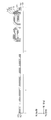
도 1 내지 도 10은 예시적인 실시예들에 따른 수직형 메모리 장치의 제조 방법의 단계들을 설명하기 위한 단면도들이다.
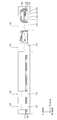
도 11 내지 도 14는 예시적인 실시예들에 따른 수직형 메모리 장치의 제조 방법의 단계들을 설명하기 위한 단면도들이다.
1 to 10 are sectional views for explaining steps of a method of manufacturing a vertical type memory device according to exemplary embodiments.
11 to 14 are sectional views for explaining steps of a method of manufacturing a vertical type memory device according to exemplary embodiments.
이하, 첨부된 도면들을 참조하여 본 발명의 바람직한 실시예들에 따른 수직형 메모리 장치 및 그 제조 방법에 대하여 상세하게 설명한다.Hereinafter, a vertical memory device according to preferred embodiments of the present invention and a method of manufacturing the same will be described in detail with reference to the accompanying drawings.
도 1 내지 도 10은 예시적인 실시예들에 따른 수직형 메모리 장치의 제조 방법의 단계들을 설명하기 위한 단면도들이다. 한편, 도 8은 도 7의 X 영역에 대한 확대 단면도이다.1 to 10 are sectional views for explaining steps of a method of manufacturing a vertical type memory device according to exemplary embodiments. 8 is an enlarged cross-sectional view of the X region in FIG.
이하에서는, 기판 상면에 실질적으로 평행한 수평 방향들 중에서 서로 교차하는 두 방향들을 각각 제1 및 제2 방향들로 정의하고, 상기 기판 상면에 실질적으로 수직한 수직 방향을 제3 방향으로 정의한다. 예시적인 실시예들에 있어서, 상기 제1 및 제2 방향들은 서로 직교할 수 있다.Hereinafter, two directions intersecting with each other among horizontal directions substantially parallel to the upper surface of the substrate are defined as first and second directions, respectively, and a vertical direction substantially perpendicular to the upper surface of the substrate is defined as a third direction. In exemplary embodiments, the first and second directions may be orthogonal to each other.
도 1을 참조하면, 제1 및 제2 영역들(I, II)을 포함하는 기판(100)의 제2 영역(II) 상에 제1 게이트 구조물 및 게이트 스페이서(150)를 형성할 수 있다.Referring to FIG. 1, a first gate structure and a
기판(100)은 실리콘, 게르마늄, 실리콘-게르마늄과 같은 반도체 물질, 또는 GaP, GaAs, GaSb 등과 같은 Ⅲ-Ⅴ족 화합물을 포함할 수 있다. 일부 실시예들에 따르면, 기판(100)은 실리콘-온-인슐레이터(Silicon-On-Insulator: SOI) 기판 또는 게르마늄-온-인슐레이터(Germanium-On-Insulator: GOI) 기판일 수 있다. The
예시적인 실시예들에 있어서, 기판(100)의 제1 및 제2 영역들(I, II)은 각각 셀 영역 및 주변 회로 영역일 수 있다.In the exemplary embodiments, the first and second regions I and II of the
상기 제1 게이트 구조물은 기판(100) 상에 게이트 절연막, 폴리실리콘 막, 금속막, 및 게이트 마스크 막을 순차적으로 적층하고 이들을 패터닝함으로써 형성될 수 있다. 이에 따라, 상기 제1 게이트 구조물은 순차적으로 적층된 게이트 절연 패턴(110), 제1 폴리실리콘 패턴(120), 제1 금속 패턴(130), 및 제1 게이트 마스크(140)를 포함할 수 있다. 이때, 제1 폴리실리콘 패턴(120) 및 제1 금속 패턴(130)은 제1 게이트 전극을 정의할 수 있다.The first gate structure may be formed by sequentially laminating a gate insulating film, a polysilicon film, a metal film, and a gate mask film on the
게이트 스페이서(150)는 상기 제1 게이트 구조물을 커버하는 게이트 스페이서 막을 기판(100) 상에 형성한 후, 이를 이방성 식각함으로써 상기 게이트 스페이서의 측벽에 형성될 수 있다.The
게이트 절연 패턴(110)은 예를 들어, 실리콘 산화물과 같은 산화물을 포함하도록 형성될 수 있고, 제1 폴리실리콘 패턴(120)은 p형 불순물 혹은 n형 불순물이 도핑된 폴리실리콘을 포함하도록 형성될 수 있으며, 제1 금속 패턴(130)은 예를 들어, 텅스텐, 탄탈륨, 티타늄 등의 금속을 포함하도록 형성될 수 있고, 제1 게이트 마스크(140)는 예를 들어, 실리콘 산화물과 같은 산화물을 포함하도록 형성될 수 있다. 한편, 게이트 스페이서(150)는 예를 들어, 실리콘 산화물과 같은 산화물을 포함하도록 형성될 수 있으며, 이에 따라 제1 게이트 마스크(140) 및/또는 게이트 절연 패턴(110)에 병합될 수도 있다.The
도 2를 참조하면, 기판(100) 상에 상기 제1 게이트 구조물을 커버하는 제1 절연막 및 식각 저지막을 형성한 후, 이들을 패터닝하여, 기판(100)의 제1 영역(I) 상에 순차적으로 적층된 제1 절연 패턴(162) 및 제1 희생 패턴(172)을 형성하고, 기판(100)의 제2 영역(II) 상에 순차적으로 적층된 제2 절연 패턴(164) 및 식각 저지 패턴(174)을 형성할 수 있다.Referring to FIG. 2, a first insulating film and an etching stopper film covering the first gate structure are formed on a
예시적인 실시예들에 있어서, 제1 절연 패턴(162) 및 제1 희생 패턴(172)은 상부에서 보았을 때, 기판(100)의 제1 영역(I) 상에 직사각 형상을 갖도록 형성될 수 있으며, 제2 절연 패턴(164) 및 식각 저지 패턴(174)은 상부에서 보았을 때, 기판(100)의 제2 영역(II) 상에서 상기 제1 게이트 구조물을 커버하도록 형성될 수 있다.In the exemplary embodiments, the
상기 제1 절연막은 예를 들어, 실리콘 산화물과 같은 산화물을 포함하도록 형성될 수 있으며, 이에 따라 제1 게이트 마스크(140) 및/또는 게이트 스페이서(150)에 병합될 수도 있다. 상기 식각 저지막은 예를 들어, 실리콘 질화물과 같은 질화물을 포함하도록 형성될 수 있다.The first insulating layer may be formed to include an oxide such as, for example, silicon oxide, and thus may be incorporated into the
이후, 제2 절연 패턴(164) 및 식각 저지 패턴(174)에 의해 커버되지 않은 기판(100)의 제2 영역(II) 상부에 불순물을 주입하여 제1 불순물 영역(도시하지 않음)을 형성할 수 있다.Thereafter, a first impurity region (not shown) is formed by implanting impurities into the upper portion of the second region II of the
도 3을 참조하면, 기판(100) 상에 제1 및 제2 절연 패턴들(162, 164), 제1 희생 패턴(172), 및 식각 저지 패턴(174)을 커버하는 제1 층간 절연막(180)을 형성한 후, 기판(100)의 제1 영역(I) 상의 제1 층간 절연막(180) 일부, 및 그 하부의 제1 희생 패턴(172) 및 제1 절연 패턴(162) 부분을 제거하여 기판(100)의 제1 영역(I)을 노출시키는 제1 개구(192)를 형성하고, 기판(100)의 제2 영역(II) 상의 제1 층간 절연막(180) 일부를 제거하여 기판(100)의 제2 영역(II)을 노출시키는 제2 개구(194)를 형성할 수 있다. A first
즉, 제2 개구(194)는 기판(100)의 제2 영역(II) 상에서 제2 절연 패턴(164) 및 식각 저지 패턴(174)이 형성되지 않은 상기 제1 게이트 구조물에 인접한 제1 층간 절연막(180) 부분을 제거하여 형성될 수 있다.That is, the
한편, 제1 개구(192)는 상기 제1 및 제2 방향들을 따라 각각 복수 개로 형성될 수 있으며, 이에 따라 제1 개구 어레이(array)가 정의될 수 있다. Meanwhile, the
예시적인 실시예들에 있어서, 제1 및 제2 개구들(192, 194)을 형성할 때, 기판(100)의 제1 및 제2 영역들(I, II) 상부도 함께 부분적으로 제거될 수 있다. In the exemplary embodiments, when forming the first and
이후, 선택적 에피택시얼 성장(Selective Epitaxial Growth: SEG) 공정을 수행하여, 제1 및 제2 개구들(192, 194)을 부분적으로 채우는 제1 및 제2 에피택시얼 층들(202, 204)을 각각 형성할 수 있다.Thereafter, a Selective Epitaxial Growth (SEG) process is performed to form first and second
예시적인 실시예들에 있어서, 상기 선택적 에피택시얼 성장(SEG) 공정은 실리콘 소스 가스, 게르마늄 소스 가스, 식각 가스 및 캐리어 가스를 기판(100) 상으로 공급하여 수행될 수 있다. 상기 선택적 에피택시얼 성장(SEG) 공정은 상기 실리콘 소스 가스로서 예를 들어, 실란(SiH4) 가스, 다이실란(Si2H6) 가스, 디클로로실란(SiH2Cl2) 가스 등을 사용할 수 있고, 상기 게르마늄 소스 가스로서 예를 들어, 저메인(GeH4) 가스를 사용할 수 있으며, 상기 식각 가스로서 염화수소(HCl) 가스를 사용할 수 있고, 상기 캐리어 가스로서 수소(H2) 가스를 사용할 수 있다. 이에 따라, 각 제1 및 제2 에피택시얼 층들(202, 204)로서 단결정의 실리콘-게르마늄 층이 형성될 수 있다. In the exemplary embodiments, the selective epitaxial growth (SEG) process may be performed by supplying a silicon source gas, a germanium source gas, an etch gas, and a carrier gas onto the
일 실시예에 있어서, 상기 선택적 에피택시얼 성장(SEG) 공정은 p형 불순물 소스 가스, 예를 들어, 디보란(B2H6) 가스를 함께 사용할 수도 있으며, 이에 따라 각 제1 및 제2 에피택시얼 층들(202, 204)로서 p형 불순물이 도핑된 단결정 실리콘-게르마늄 층이 형성될 수도 있다. In one embodiment, the selective epitaxial growth (SEG) process may use a p-type impurity source gas, for example, diborane (B 2 H 6 ) gas, A single crystal silicon-germanium layer doped with a p-type impurity may be formed as the
이와는 달리, 별도의 도핑 공정에 의해, 제2 에피택시얼 층(204)에만 p형 불순물을 도핑할 수도 있으며, 이에 따라 제2 에피택시얼 층(204)은 피모스(Positive-channel Metal Oxide Semiconductor: PMOS) 트랜지스터의 소스/드레인 영역 역할을 수행할 수 있다.Alternatively, the second
다른 실시예들에 있어서, 상기 선택적 에피택시얼 성장(SEG) 공정은 실리콘 소스 가스, 탄소 소스 가스, 식각 가스 및 캐리어 가스를 사용하여 수행될 수 있으며, 이에 따라 각 제1 및 제2 에피택시얼 층들(202, 204)로서 단결정 실리콘 탄화물 층이 형성될 수 있다. 상기 선택적 에피택시얼 성장(SEG) 공정에서는, 상기 실리콘 소스 가스로서 예를 들어, 실란(SiH4) 가스, 다이실란(Si2H6) 가스, 디클로로실란(SiH2Cl2) 가스 등을 사용할 수 있고, 상기 탄소 소스 가스로서 예를 들어, SiH3CH3 가스를 사용할 수 있으며, 상기 식각 가스로서 염화수소(HCl) 가스를 사용할 수 있고, 상기 캐리어 가스로서 수소(H2) 가스를 사용할 수 있다. In other embodiments, the selective epitaxial growth (SEG) process may be performed using a silicon source gas, a carbon source gas, an etch gas, and a carrier gas, whereby each first and second epitaxial growth A single crystal silicon carbide layer may be formed as the
이와는 달리, 상기 선택적 에피택시얼 성장(SEG) 공정은 실리콘 소스 가스, 식각 가스 및 캐리어 가스를 사용하여 수행될 수 있으며, 이에 따라 각 제1 및 제2 에피택시얼 층들(202, 204)로서 단결정 실리콘 층이 형성될 수 있다.Alternatively, the selective epitaxial growth (SEG) process may be performed using a silicon source gas, an etch gas, and a carrier gas, thereby forming a single crystal (first and second epitaxial layer) A silicon layer may be formed.
일 실시예에 있어서, n형 불순물 소스 가스, 예를 들어, 포스핀(PH3) 가스 등이 함께 사용되어 n형 불순물이 도핑된 단결정 실리콘 탄화물 층 혹은 n형 불순물이 도핑된 단결정 실리콘 층이 형성될 수도 있다.In one embodiment, an n-type impurity source gas, for example, a phosphine (PH3) gas or the like is used together to form a monocrystalline silicon carbide layer doped with an n-type impurity or a monocrystalline silicon layer doped with an n-type impurity It is possible.
이와는 달리, 별도의 도핑 공정에 의해, 제2 에피택시얼 층(204)에만 n형 불순물을 도핑할 수도 있으며, 이에 따라 제2 에피택시얼 층(204)은 엔모스(Negative-channel Metal Oxide Semiconductor: NMOS) 트랜지스터의 소스/드레인 영역 역할을 수행할 수 있다.Alternatively, the second
예시적인 실시예들에 있어서, 제1 에피택시얼 층(202)의 상면은 제2 에피택시얼 층(204)의 상면보다 높을 수 있으나, 본 발명의 개념은 반드시 이에 한정되지는 않는다.In the exemplary embodiments, the top surface of the first
도 4를 참조하면, 제1 및 제2 개구들(192, 194)의 나머지 부분을 채우는 제2 층간 절연막을 제1 및 제2 에피택시얼 층들(202, 204) 및 제1 층간 절연막(180) 상에 형성한 후, 이를 평탄화할 수 있다. 상기 평탄화 공정은 화학 기계적 연마(Chemical Mechanical Polishing: CMP) 공정 및/또는 에치 백(etch back) 공정을 통해 수행될 수 있다.Referring to FIG. 4, a second interlayer insulating film filling the remaining portions of the first and
예시적인 실시예들에 있어서, 상기 제2 층간 절연막은 제1 층간 절연막(180)과 실질적으로 동일한 물질, 예를 들어 실리콘 질화물을 포함하도록 형성할 수 있으며, 이에 따라 제1 층간 절연막(180)에 병합될 수 있다. 이하에서는 상기 제2 층간 절연막은 별도로 표시하지 않기로 한다.In the exemplary embodiments, the second interlayer insulating film may be formed to include substantially the same material as the first
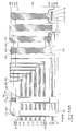
이후, 제1 층간 절연막(180) 상에 희생막(220) 및 제2 절연막(210)을 교대로 반복적으로 적층할 수 있다. 이에 따라, 복수의 희생막들(220) 및 복수의 제2 절연막들(210)이 상기 제3 방향을 따라 교대로 적층될 수 있다. 도 4에는 예시적으로, 6개 층의 제2 절연막들(210) 및 6개 층의 희생막들(220)이 교대로 형성된 것이 도시되어 있으나, 제2 절연막(210) 및 희생막(220)의 개수는 이에 한정되지 않으며, 각각 더 많거나 혹은 더 적은 개수로 형성될 수도 있다.Thereafter, the
제2 절연막(210) 및 희생막(220)은, 예를 들어, 화학 기상 증착(Chemical Vapor Deposition: CVD) 공정, 플라스마 화학 기상 증착(Plasma Enhanced Chemical Vapor Deposition: PECVD) 공정, 원자층 증착(Atomic Layer Deposition: ALD) 공정 등을 통해 형성할 수 있다. The second
제2 절연막(210)은 예를 들어, 피이-테오스(PE-TEOS), 고밀도 플라스마(HDP) 산화물 또는 피이오엑스(PEOX) 등과 같은 실리콘 산화물을 포함하도록 형성될 수 있다. 희생막(220)은 제2 절연막(210)에 대해 식각 선택비를 갖는 물질, 예를 들어, 실리콘 질화물을 포함하도록 형성될 수 있다. The second
도 5를 참조하면, 최상층에 형성된 제2 절연막(210)을 부분적으로 커버하는 포토레지스트 패턴(도시되지 않음)을 최상층 제2 절연막(210) 상에 형성한 후, 이를 식각 마스크로 사용하여 최상층 제2 절연막(210) 및 그 하부의 최상층 희생막(220)을 식각한다. 이에 따라, 최상층 희생막(220) 하부에 형성된 제2 절연막(210)의 일부가 노출될 수 있다. 상기 포토레지스트 패턴의 면적을 일정한 비율로 축소시킨 후, 이를 식각 마스크로 사용하여 최상층 제2 절연막(210), 최상층 희생막(220), 상기 노출된 제2 절연막(210), 및 그 하부의 희생막(220)을 다시 식각하는 트리밍(trimming) 공정을 수행한다. 상기 트리밍 공정을 반복적으로 수행함으로써, 기판(100)의 제1 영역(I) 상에는 순차적으로 적층된 제2 희생 패턴(225) 및 제3 절연 패턴(215)으로 각각 구성되는 복수 개의 계단들을 포함하는 계단 구조물이 형성될 수 있다. 5, a photoresist pattern (not shown) for partially covering the second
예시적인 실시예들에 있어서, 상기 계단 구조물에 포함된 계단들은 하층에서 상층으로 갈수록 일정한 비율로 감소하는 면적을 가질 수 있다. 또한 상기 계단 구조물의 최하층 계단은 상부에서 보았을 때, 제1 절연 패턴(162) 및 제1 희생 패턴(172)을 포함하는 계단보다 작은 면적을 가질 수 있다.In exemplary embodiments, the steps included in the step structure may have an area decreasing at a constant rate from the lower layer to the upper layer. Also, the lowest step of the step structure may have a smaller area than the step including the
도 6을 참조하면, 상기 계단 구조물을 커버하는 제3 층간 절연막을 제1 층간 절연막(180) 상에 형성하고, 최상층의 제3 절연 패턴(215)의 상면이 노출될 때까지 상기 제3 층간 절연막을 평탄화함으로써, 상기 계단 구조물의 측벽을 커버하는 제3 층간 절연 패턴(230)을 형성할 수 있다.Referring to FIG. 6, a third interlayer insulating film covering the step structure is formed on the first interlayer
상기 제3 층간 절연막은 예를 들어, 실리콘 산화물과 같은 산화물을 포함하도록 형성될 수 있으며, 이에 따라 제3 층간 절연 패턴(230)은 제3 절연 패턴(215) 및/또는 제1 층간 절연막(180)과 병합될 수도 있다. The third
이후, 상기 계단 구조물의 상면 및 제3 층간 절연 패턴(230)의 상면에 제4 층간 절연막(240)을 형성할 수 있다.Then, a fourth
제4 층간 절연막(240)은 예를 들어, 실리콘 산화물과 같은 산화물을 포함하도록 형성될 수 있으며, 이에 따라 제3 층간 절연 패턴(230) 및/또는 최상층의 제3 절연 패턴(215)에 병합될 수도 있다. The fourth
이후, 제4 층간 절연막(240) 상에 제1 마스크(도시되지 않음)를 형성한 후, 이를 식각 마스크로 사용하여 하부의 제4 층간 절연막(240), 제3 절연 패턴들(215), 제2 희생 패턴들(225), 및 제1 층간 절연막(180)을 식각함으로써, 이들을 적어도 부분적으로 관통하여 기판(100)의 제1 영역(I) 상에 형성된 제1 에피택시얼 층(202) 상면을 노출시키는 채널 홀(hole)(250)을 형성할 수 있다. Thereafter, a first mask (not shown) is formed on the fourth
채널 홀(250)은 상기 제1 및 제2 방향들을 따라 각각 복수 개로 형성될 수 있으며, 상기 제1 개구 어레이에 대응하여 채널 홀 어레이(array)가 정의될 수 있다. A plurality of channel holes 250 may be formed along the first and second directions, and a channel hole array may be defined corresponding to the first plurality of aperture arrays.
도 7 및 도 8을 참조하면, 먼저 상기 제1 마스크를 제거한 후, 채널 홀들(250)의 측벽, 제1 에피택시얼 층(202)의 상면, 및 제4 층간 절연막(240)의 상면에 제1 블로킹막, 전하 저장막, 터널 절연막 및 제1 스페이서 막(도시되지 않음)을 순차적으로 형성하고, 상기 제1 스페이서 막을 이방성 식각하여 채널 홀들(250)의 측벽 상에만 잔류하는 제1 스페이서(도시되지 않음)를 형성한 후, 상기 제1 스페이서를 식각 마스크로 사용하여 상기 터널 절연막, 상기 전하 저장막 및 상기 제1 블로킹막을 식각함으로써, 제1 에피택시얼 층(202) 및 채널 홀들(250)의 측벽 상에 저면 중앙부가 뚫린 컵 형상을 갖는 터널 절연 패턴(290), 전하 저장 패턴(280) 및 제1 블로킹 패턴(270)을 각각 형성할 수 있다. 이때, 제1 에피택시얼 층(202)의 상부도 부분적으로 함께 제거될 수 있다. 한편, 터널 절연 패턴(290), 전하 저장 패턴(280) 및 제1 블로킹 패턴(270)은 함께 전하 저장 구조물(300)을 형성할 수 있다.7 and 8, after removing the first mask, a first mask is formed on the sidewalls of the channel holes 250, the upper surface of the
상기 제1 블로킹막은 예를 들어, 실리콘 산화물과 같은 산화물을 포함하도록 형성할 수 있고, 상기 전하 저장막은 예를 들어, 실리콘 질화물과 같은 질화물을 포함하도록 형성할 수 있으며, 상기 터널 절연막은 예를 들어, 실리콘 산화물과 같은 산화물을 포함하도록 형성할 수 있고, 상기 제1 스페이서 막은 예를 들어 실리콘 질화물과 같은 질화물을 포함하도록 형성할 수 있다. The first blocking film may be formed to include an oxide such as, for example, silicon oxide, and the charge storage film may be formed to include nitride, for example, silicon nitride. The tunnel insulating film may be formed, for example, , An oxide such as silicon oxide, and the first spacer film may be formed to include a nitride such as, for example, silicon nitride.
상기 제1 스페이서를 제거한 후, 노출된 제1 에피택시얼 층(202), 터널 절연 패턴(290), 및 제4 층간 절연막(240) 상에 채널막을 형성하고, 채널 홀들(250)의 나머지 부분을 충분히 채우는 충전막을 상기 채널막 상에 형성한다. After removing the first spacers, a channel film is formed on the exposed
상기 채널막은 불순물이 도핑되거나 또는 도핑되지 않은 폴리실리콘 혹은 비정질 실리콘을 포함하도록 형성할 수 있다. 상기 채널막이 비정질 실리콘을 포함하도록 형성되는 경우, 이후 레이저 에피택시얼 성장(Laser Epitaxial Growth: LEG) 공정 혹은 고상 에피택시(Solid Phase Epitaxy: SPE) 공정을 추가적으로 수행하여 이를 결정질 실리콘으로 변환시킬 수 있다. 상기 충전막은 예를 들어, 실리콘 산화물과 같은 산화물을 포함하도록 형성할 수 있다.The channel film may be formed to include impurity-doped or undoped polysilicon or amorphous silicon. When the channel layer is formed to include amorphous silicon, a laser epitaxial growth (LEG) process or a solid phase epitaxy (SPE) process may be further performed to convert the channel layer to crystalline silicon . The filling film may be formed to include an oxide such as, for example, silicon oxide.
이후, 제4 층간 절연막(240)의 상면이 노출될 때까지 상기 충전막 및 상기 채널막을 평탄화함으로써, 각 채널 홀들(250)의 나머지 부분을 채우는 충전 패턴(320)을 형성할 수 있으며, 상기 채널막은 채널(310)로 변환될 수 있다. Thereafter, the filling film and the channel film are planarized until the upper surface of the fourth
이에 따라, 각 채널 홀들(250) 내 제1 에피택시얼 층(202) 상에는 전하 저장 구조물(300), 채널(310) 및 충전 패턴(320)이 순차적으로 적층될 수 있다. 이때, 전하 저장 구조물(300)은 저면 중앙부가 뚫린 컵 형상으로 형성될 수 있고, 채널(310)은 컵 형상으로 형성될 수 있으며, 충전 패턴(320)은 필라(pillar) 형상으로 형성될 수 있다. Accordingly, the
채널(310)이 형성되는 채널 홀들(250)이 상기 채널 홀 어레이를 정의함에 따라, 채널(310) 역시 이에 대응하여 채널 어레이를 정의할 수 있다. 한편, 채널(310) 하부에 형성되는 제1 에피택시얼 층(202)은 하부 채널로, 채널(310)은 상부 채널로 각각 지칭될 수도 있다.As the channel holes 250 in which the
이후, 충전 패턴(320), 채널(310), 및 전하 저장 구조물(300)로 구성되는 제1 구조물의 상부를 제거하여 트렌치(도시되지 않음)를 형성하고, 상기 트렌치를 채우는 캐핑 패턴(330)을 형성할 수 있다.Thereafter, a
구체적으로, 상기 제1 구조물의 상부를 에치 백 공정을 통해 제거하여 상기 트렌치를 형성한 후, 상기 트렌치를 채우는 캐핑막을 상기 제1 구조물 및 제4 층간 절연막(240) 상에 형성하고, 제4 층간 절연막(240)의 상면이 노출될 때까지 상기 캐핑막의 상부를 평탄화하여 캐핑 패턴(330)을 형성할 수 있다. 예시적인 실시예들에 있어서, 상기 캐핑막은 불순물이 도핑되거나 또는 도핑되지 않은 폴리실리콘 혹은 비정질 실리콘을 포함하도록 형성될 수 있으며, 상기 캐핑막이 비정질 실리콘을 포함하도록 형성되는 경우, 이를 결정화시키는 공정이 추가적으로 수행될 수도 있다. Specifically, after the upper portion of the first structure is removed through the etch-back process to form the trench, a capping film filling the trench is formed on the first structure and the fourth
한편, 각 채널 홀들(250) 내부에 형성되는 상기 제1 구조물, 제1 에피택시얼 층(202) 및 캐핑 패턴(330)은 제2 구조물을 정의할 수 있다.Meanwhile, the first structure, the
도 9를 참조하면, 제4 층간 절연막(240) 및 캐핑 패턴(330) 상에 제5 층간 절연막(340)을 형성한다. 제5 층간 절연막(340) 상에 제2 마스크(도시되지 않음)를 형성한 후, 이를 식각 마스크로 사용하여 하부의 제4 및 제5 층간 절연막들(240, 340), 제3 절연 패턴들(215), 및 제2 희생 패턴들(225)을 관통하는 제3 개구(도시하지 않음)를 형성하여 기판(100) 상면을 노출시킨다. 제5 층간 절연막(340)은 예를 들어, 실리콘 산화물과 같은 산화물을 포함하도록 형성될 수 있으며, 이에 따라 하부의 제4 층간 절연막(240)에 병합될 수도 있다.Referring to FIG. 9, a fifth
예시적인 실시예들에 있어서, 상기 제3 개구는 기판(100)의 제1 영역(I) 상에서 상기 제1 방향을 따라 연장되도록 형성될 수 있으며, 이에 따라 상기 제2 방향을 따라 복수 개로 형성될 수 있다. In the exemplary embodiments, the third opening may be formed to extend along the first direction on the first region I of the
상기 제2 마스크를 제거한 후, 상기 제3 개구에 의해 노출된 제1 및 제2 희생 패턴들(172, 225)을 제거하여, 각 층의 제3 절연 패턴들(215) 사이 및 제1 절연 패턴(162)과 제1 층간 절연막(180) 사이에 갭(도시하지 않음)을 형성할 수 있으며, 상기 갭에 의해 제1 블로킹 패턴(270)의 외측벽 일부 및 제1 에피택시얼 층(202)의 측벽 일부가 노출될 수 있다. 예시적인 실시예들에 따르면, 인산 혹은 황산을 포함하는 식각액을 사용하는 습식 식각 공정을 통해 상기 제3 개구에 의해 노출된 제1 및 제2 희생 패턴들(172, 225)을 제거할 수 있다.After the second mask is removed, the first and second sacrificial patterns (172, 225) exposed by the third opening are removed to form a gap between the third insulating patterns (215) A gap (not shown) may be formed between the first
이후, 노출된 제1 블로킹 패턴(270)의 외측벽, 노출된 제1 에피택시얼 층(202)의 측벽, 상기 갭의 내벽, 제1 및 제3 절연 패턴들(162, 215)의 표면, 노출된 기판(100) 상면, 및 제5 층간 절연막(340)의 상면에 제2 블로킹막(370)을 형성하고, 제2 블로킹 막(370) 상에 게이트 배리어막을 형성한 후, 상기 갭의 나머지 부분을 충분히 채우는 게이트 도전막을 상기 게이트 배리어막 상에 형성한다.Thereafter, the outer wall of the exposed first blocking
제2 블로킹 막(370)은 예를 들어, 알루미늄 산화물, 하프늄 산화물, 란탄 산화물, 란탄 알루미늄 산화물, 란탄 하프늄 산화물, 하프늄 알루미늄 산화물, 티타늄 산화물, 탄탈륨 산화물, 지르코늄 산화물 등의 금속 산화물을 포함하도록 형성할 수 있다. 상기 게이트 도전막은 예를 들어, 텅스텐, 티타늄, 탄탈륨, 백금 등의 전기 저항이 낮은 금속을 포함하도록 형성될 수 있다. 상기 게이트 배리어막은 예를 들어, 티타늄 질화물, 탄탈륨 질화물 등의 금속 질화물을 포함하도록 형성될 수 있다. 이와는 달리, 상기 게이트 배리어막은 금속을 포함하는 제1 층 및 금속 질화물을 포함하는 제2 층으로 구성될 수도 있다. The
이후, 상기 게이트 도전막 및 상기 게이트 배리어막을 부분적으로 제거하여, 상기 갭 내부에 각각 게이트 도전 패턴 및 게이트 배리어 패턴을 형성할 수 있으며, 이들은 함께 셀 게이트 전극을 형성할 수 있다. 예시적인 실시예들에 따르면, 상기 게이트 도전막 및 상기 게이트 배리어막은 습식 식각 공정을 통해 부분적으로 제거될 수 있다.Thereafter, the gate conductive film and the gate barrier film may be partially removed to form a gate conductive pattern and a gate barrier pattern, respectively, in the gap, and they can form a cell gate electrode. According to exemplary embodiments, the gate conductive film and the gate barrier film can be partially removed through a wet etching process.
예시적인 실시예들에 있어서, 상기 셀 게이트 전극은 상기 제1 방향으로 연장될 수 있으며, 상기 제2 방향을 따라 복수 개로 형성될 수 있다. 즉, 상기 제1 방향으로 연장되는 상기 각 복수 개의 셀 게이트 전극들은 상기 제3 개구에 의해 상기 제2 방향으로 서로 이격될 수 있다. In exemplary embodiments, the cell gate electrodes may extend in the first direction, and may be formed in a plurality of along the second direction. That is, each of the plurality of cell gate electrodes extending in the first direction may be spaced apart from each other in the second direction by the third opening.
상기 셀 게이트 전극 중에서 상기 제1 방향으로의 각 말단 부분은 패드(pad)로 지칭될 수도 있다. 즉, 상기 셀 게이트 전극은 상기 제3 방향을 따라 서로 이격되도록 복수 개로 적층될 수 있으며, 또한 각 셀 게이트 전극들은 기판(100)의 제1 영역(I) 상에서 상기 제1 방향으로 연장될 수 있다. 이때, 상기 셀 게이트 전극들의 상기 제1 방향으로의 길이는 상부로 갈수록 점차 작아질 수 있으며, 이에 따라 이들은 전체적으로 계단 형상을 가질 수 있다. Each end portion of the cell gate electrode in the first direction may be referred to as a pad. That is, the cell gate electrodes may be stacked to be spaced apart from each other along the third direction, and each cell gate electrode may extend in the first direction on the first region I of the
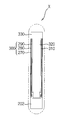
상기 셀 게이트 전극은 상기 제3 방향을 따라 순차적으로 형성된 제2 내지 제4 게이트 전극들(403, 405, 407)을 포함할 수 있다. 이때, 제2 게이트 전극(403)은 그라운드 선택 라인(Ground Selection Line: GSL) 역할을 수행할 수 있고, 제3 게이트 전극(405)은 워드 라인 역할을 수행할 수 있으며, 제4 게이트 전극(407)은 스트링 선택 라인(String Selection Line: SSL) 역할을 수행할 수 있다. 이때, 제2 게이트 전극(403)은 최하층에 형성될 수 있으며, 각 제3 및 제4 게이트 전극들(405, 407)은 제2 게이트 전극(403) 상에서 1개 혹은 복수 개의 층들에 형성될 수 있다. 예시적인 실시예들에 있어서, 제4 게이트 전극(407)은 최상층 및 그 하부의 1개의 층에 형성될 수 있으며, 제3 게이트 전극(405)은 제2 게이트 전극(403) 및 제4 게이트 전극(407) 사이에서 짝수 개의 층들에 형성될 수 있다. The cell gate electrode may include second to
이에 따라, 제2 게이트 전극(403)은 제1 에피택시얼 층(202)에 인접하여 형성될 수 있고, 각 제3 및 제4 게이트 전극들(405, 407)은 채널(310)에 인접하여 형성될 수 있다. 즉, 제1 에피택시얼 층(202)은 제2 게이트 전극(203)을 관통하여 이를 포함하는 그라운드 선택 트랜지스터(GST)의 채널 역할을 수행할 수 있으며, 채널(310)은 제3 및 제4 게이트 전극들(405, 407)을 관통하여 셀 트랜지스터 및 스트링 선택 트랜지스터(SST)의 채널 역할을 수행할 수 있다.A
제2 게이트 전극(403)은 제2 게이트 도전 패턴(393) 및 이의 상하면 및 측벽 일부를 커버하는 제2 게이트 배리어 패턴(383)을 포함할 수 있고, 제3 게이트 전극(405)은 제3 게이트 도전 패턴(395) 및 이의 상하면 및 측벽 일부를 커버하는 제3 게이트 배리어 패턴(385)을 포함할 수 있으며, 제4 게이트 전극(407)은 제4 게이트 도전 패턴(397) 및 이의 상하면 및 측벽 일부를 커버하는 제4 게이트 배리어 패턴(387)을 포함할 수 있다. The
이후, 상기 제3 개구에 의해 노출된 기판(100) 상부에 불순물을 주입하여 제2 불순물 영역(도시하지 않음)을 형성할 수 있다. 예시적인 실시예들에 따르면, 상기 불순물은 인, 비소와 같은 n형 불순물을 포함할 수 있다. Then, a second impurity region (not shown) may be formed by implanting impurities on the
이후, 상기 제3 개구에 의해 노출된 기판(100) 상면, 상기 제3 개구의 측벽, 및 제5 층간 절연막(340) 상면에 제2 스페이서 막(도시되지 않음)을 형성한 후, 상기 제2 스페이서 막을 이방성 식각함으로써, 상기 제3 개구의 측벽 상에 제2 스페이서(도시하지 않음)를 형성할 수 있다. 이에 따라 기판(100) 상부에 형성된 상기 제2 불순물 영역의 일부가 노출될 수 있다. 상기 제2 스페이서 막은 예를 들어, 실리콘 산화물과 같은 산화물을 포함하도록 형성할 수 있다.Thereafter, a second spacer film (not shown) is formed on the upper surface of the
이후, 노출된 상기 제2 불순물 영역 상에 상기 제3 개구의 나머지 부분을 채우는 공통 소스 라인(Common Source Line: CSL)(도시하지 않음)을 형성할 수 있다. Thereafter, a common source line (CSL) (not shown) filling the remaining portion of the third opening on the exposed second impurity region may be formed.
예시적인 실시예들에 따르면, 상기 제3 개구를 채우는 도전막을 상기 노출된 제2 불순물 영역 상면, 상기 제2 스페이서, 및 제5 층간 절연막(340) 상에 형성한 후, 제5 층간 절연막(340)의 상면이 노출될 때까지 상기 도전막 상부를 평탄화함으로써, 상기 공통 소스 라인(CSL)을 형성할 수 있다. 이때, 제5 층간 절연막(340) 상면에 형성된 상기 제2 블로킹 막 부분도 함께 제거될 수 있다. 상기 도전막은 금속, 금속 질화물 및/또는 금속 실리사이드를 포함하도록 형성될 수 있다.According to exemplary embodiments, a conductive film filling the third opening is formed on the exposed second impurity region upper surface, the second spacer, and the fifth
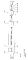
상기 공통 소스 라인(CSL)은 상기 제3 개구 내에 형성되어 하부의 상기 제2 불순물 영역 상면에 접촉할 수 있다.The common source line (CSL) may be formed in the third opening and contact the upper surface of the second impurity region at the bottom.
도 10을 참조하면, 제5 층간 절연막(340), 상기 공통 소스 라인(CSL), 상기 제2 스페이서 및 제2 블로킹 막(370) 상에 제6 층간 절연막(440)을 형성한 후, 제5 및 제6 층간 절연막들(340, 440)을 관통하여 캐핑 패턴들(330) 상면에 각각 접촉하는 제1 콘택 플러그들(452)을 형성할 수 있고, 제4 내지 제6 층간 절연막들(240, 340, 440), 제3 절연 패턴(215), 제2 블로킹 막(370), 및 게이트 배리어 패턴들(383, 385, 387)을 관통하여 게이트 도전 패턴들(393, 395, 397)의 상면에 각각 접촉하는 제2 콘택 플러그들(454)을 형성할 수 있으며, 제1 층간 절연막(180), 제3 층간 절연 패턴(230), 및 제4 내지 제6 층간 절연막들(240, 340, 440)을 관통하여 제2 에피택시얼 층(204) 상면에 접촉하는 제3 콘택 플러그(456)를 형성할 수 있고, 제1 층간 절연막(180), 제3 층간 절연 패턴(230), 및 제4 내지 제6 층간 절연막들(240, 340, 440), 식각 저지 패턴(174), 제2 절연 패턴(164), 및 제1 게이트 마스크(140)을 관통하여 제1 금속 패턴(130) 상면에 접촉하는 제4 콘택 플러그(458)를 형성할 수 있다. 10, a sixth
이때, 각 제2 콘택 플러그들(454)은 상기 계단 형상의 각 패드들 상에 형성될 수 있다. 즉, 각 제2 콘택 플러그들(454)은 상층 패드들에 의해 커버되지 않는 각 패드들 부분 상에 형성될 수 있다. At this time, each
제6 층간 절연막(440)은 예를 들어, 실리콘 산화물과 같은 산화물을 포함하도록 형성될 수 있으며, 이에 따라 하부의 제5 층간 절연막(340)에 병합될 수도 있다. 제1 내지 제4 콘택 플러그들(452, 454, 456, 458)은 예를 들어, 텅스텐, 티타늄, 탄탈륨, 구리, 알루미늄 등의 금속 및/또는 티타늄 질화물, 탄탈륨 질화물, 텅스텐 질화물 등의 금속 질화물을 포함하도록 형성될 수 있다. The sixth
이후, 제6 층간 절연막(440), 및 제1 내지 제4 콘택 플러그들(452, 454, 456, 458) 상에 제7 층간 절연막(460)을 형성하고, 이를 관통하여 제1 내지 제4 콘택 플러그들(452, 454, 456, 458) 상면에 각각 접촉하는 제1 내지 제4 배선들(472, 474, 476, 478)을 각각 형성함으로써 상기 수직형 메모리 장치를 완성할 수 있다.Thereafter, a seventh
예시적인 실시예들에 있어서, 제1 배선(472)은 상기 제2 방향으로 연장될 수 있으며, 상기 수직형 메모리 장치의 비트 라인 역할을 수행할 수 있다.In the exemplary embodiments, the
제7 층간 절연막(460)은 예를 들어, 실리콘 산화물과 같은 산화물을 포함하도록 형성될 수 있으며, 이에 따라 하부의 제6 층간 절연막(440)에 병합될 수도 있다. 또한, 제1 내지 제4 배선들(472, 474, 476, 478)은 예를 들어, 텅스텐, 티타늄, 탄탈륨, 구리, 알루미늄 등의 금속 및/또는 티타늄 질화물, 탄탈륨 질화물, 텅스텐 질화물 등의 금속 질화물을 포함하도록 형성될 수 있다. The seventh
전술한 바와 같이, 예시적인 실시예들에 따른 상기 수직형 메모리 장치의 제조 공정에서, 셀 영역에서 GST의 채널 역할을 수행하는 제1 에피택시얼 층(202)과 주변 회로 영역에서 트랜지스터의 소스/드레인 역할을 수행하는 제2 에피택시얼 층(204)을 하나의 선택적 에피택시얼 성장(SEG)을 통해 형성할 수 있다. 이에 따라, 전체 공정이 단순해질 수 있다.As described above, in the manufacturing process of the vertical memory device according to the exemplary embodiments, the
한편, 전술한 공정을 통해 제조된 수직형 메모리 장치는 기판(100)의 상기 주변 회로 영역 상에 형성되어 제1 게이트 전극(120, 130)을 포함하는 상기 제1 게이트 구조물, 기판(100)의 상기 셀 영역 상에서 복수의 층들에 순차적으로 형성된 제2 내지 제4 게이트 전극들(403, 405, 407), 기판(100)의 상기 셀 영역 상에 형성되어 제2 게이트 전극(403)을 관통하는 제1 에피택시얼 층(202), 제1 에피택시얼 층(202) 상에 수직 방향을 따라 연장되어 제3 및 제4 게이트 전극들(405, 407)을 관통하는 채널(310), 및 상기 제1 게이트 구조물에 인접한 기판(100)의 상기 주변 회로 영역 상에 형성된 제2 에피택시얼 층(204)을 포함할 수 있다.Meanwhile, the vertical memory device manufactured through the above-described process includes the first gate structure formed on the peripheral circuit region of the
이때, 제1 및 제2 에피택시얼 층들(202, 204)은 동일한 SEG 공정을 통해 형성되므로 실질적으로 서로 동일한 물질을 포함할 수 있다. Here, since the first and second
한편, 상기 수직형 메모리 장치는 상기 제1 게이트 구조물의 표면 상에 형성된 식각 저지 패턴(174)을 더 포함할 수 있다. 기판(100)의 제2 영역(II) 상에 형성되는 식각 저지 패턴(174)은 기판(100)의 제1 영역(I) 상에 형성되는 제1 희생 패턴(172)과 동일한 공정을 통해 동일한 두께로 형성되므로, 제1 희생 패턴(172)을 제거하여 형성되는 상기 갭을 채우는 제2 게이트 전극(403) 및 이의 상하면을 커버하는 제2 블로킹 패턴(370)의 두께의 합은 식각 저지 패턴(174)의 두께와 실질적으로 동일할 수 있다.Meanwhile, the vertical memory device may further include an
도 11 내지 도 14는 예시적인 실시예들에 따른 수직형 메모리 장치의 제조 방법의 단계들을 설명하기 위한 단면도들이다. 상기 제조 방법은 도 1 내지 도 10을 참조로 설명한 공정들과 실질적으로 동일하거나 유사한 공정들을 포함하므로, 이에 대한 자세한 설명은 생략한다.11 to 14 are sectional views for explaining steps of a method of manufacturing a vertical type memory device according to exemplary embodiments. The manufacturing method includes processes substantially the same as or similar to those described with reference to FIGS. 1 to 10, so that detailed description thereof will be omitted.
도 11을 참조하면, 제1 및 제2 영역들(I, II)을 포함하는 기판(100)의 제2 영역(II) 상에 상기 제1 게이트 구조물 및 게이트 스페이서(150)를 형성할 수 있으며, 또한 기판(100)의 제1 영역(I) 상에 제2 게이트 구조물을 형성할 수 있다.Referring to FIG. 11, the first gate structure and the
구체적으로, 기판(100) 상에 게이트 절연막, 폴리실리콘 막, 금속막, 및 게이트 마스크 막을 순차적으로 적층하고 이들을 패터닝함으로써, 기판(100)의 제2 영역(II) 상에 순차적으로 적층된 게이트 절연 패턴(110), 제1 폴리실리콘 패턴(120), 제1 금속 패턴(130), 및 제1 게이트 마스크(140)를 포함하는 상기 제1 게이트 구조물을 형성할 수 있으며, 기판(100)의 제2 영역(II) 상에 순차적으로 적층된 제4 절연 패턴(115), 제2 폴리실리콘 패턴(125), 제2 금속 패턴(135), 및 제2 게이트 마스크(145)를 포함하는 상기 제2 게이트 구조물을 형성할 수 있다. Specifically, a gate insulating film, a polysilicon film, a metal film, and a gate mask film are successively laminated on the
이때, 상기 제1 게이트 구조물은 순차적으로 적층된 제1 폴리실리콘 패턴(120) 및 제1 금속 패턴(130)을 포함하는 상기 제1 게이트 전극을 포함할 수 있으며, 상기 제2 게이트 구조물은 순차적으로 적층된 제2 폴리실리콘 패턴(125) 및 제2 금속 패턴(135)을 포함하는 제5 게이트 전극을 포함할 수 있다.Here, the first gate structure may include the first gate electrode including the
한편, 상기 제2 게이트 구조물 내에는 기판(100) 상면을 노출시키는 제4 개구가 형성될 수 있으며, 상기 제4 개구는 도 3을 참조로 설명한 제1 개구(192)와 같이 상기 제1 및 제2 방향들을 따라 각각 복수 개로 형성되어 제4 개구 어레이를 형성할 수 있다.A fourth opening may be formed in the second gate structure to expose an upper surface of the
이후, 기판(100)의 제2 영역(II) 상에 형성된 상기 제1 게이트 구조물의 측벽에 게이트 스페이서(150)를 더 형성할 수 있다.Thereafter,
도 12를 참조하면, 도 2를 참조로 설명한 공정들과 실질적으로 동일하거나 유사한 공정들을 수행할 수 있다.Referring to FIG. 12, it is possible to perform processes substantially identical to or similar to the processes described with reference to FIG.
다만, 기판(100)의 제1 영역(I) 상에는 제1 절연 패턴(162) 및 제1 희생 패턴(172)이 형성되지 않으며, 기판(100)의 제2 영역(II) 상에만 상기 제2 게이트 구조물을 커버하는 제2 절연 패턴(164) 및 식각 저지 패턴(174)이 순차적으로 형성될 수 있다.The first
이후, 제2 절연 패턴(164) 및 식각 저지 패턴(174)에 의해 커버되지 않은 기판(100)의 제2 영역(II) 상부에 불순물을 주입하여 제1 불순물 영역(도시하지 않음)을 형성할 수 있다.Thereafter, a first impurity region (not shown) is formed by implanting impurities into the upper portion of the second region II of the
도 13을 참조하면, 도 3을 참조로 설명한 공정들과 실질적으로 동일하거나 유사한 공정들을 수행할 수 있다.Referring to FIG. 13, substantially the same or similar processes as those described with reference to FIG. 3 can be performed.
이에 따라, 기판(100) 상에 상기 제1 및 제2 게이트 구조물들, 제2 절연 패턴(164), 및 식각 저지 패턴(174)을 커버하는 제1 층간 절연막(180)을 형성한 후, 기판(100)의 제1 영역(I) 상의 제1 층간 절연막(180) 일부를 제거하여 기판(100)의 제1 영역(I)을 노출시키는 제1 개구(192)를 형성하고, 기판(100)의 제2 영역(II) 상의 제1 층간 절연막(180) 일부를 제거하여 기판(100)의 제2 영역(II)을 노출시키는 제2 개구(194)를 형성할 수 있다. Accordingly, a first
즉, 제1 개구(192)는 상기 제2 게이트 구조물 내에 형성된 상기 제3 개구에 오버랩되는 위치에 형성될 수 있으며, 제2 개구(194)는 기판(100)의 제2 영역(II) 상에서 제2 절연 패턴(164) 및 식각 저지 패턴(174)이 형성되지 않은 상기 제2 게이트 구조물에 인접한 제1 층간 절연막(180) 부분을 제거하여 형성될 수 있다.The
이후, 선택적 에피택시얼 성장(SEG) 공정을 수행하여, 제1 및 제2 개구들(192, 194)을 부분적으로 채우는 제1 및 제2 에피택시얼 층들(202, 204)을 각각 형성할 수 있다.Thereafter, a selective epitaxial growth (SEG) process may be performed to form first and second
한편, 제1 층간 절연막(180)은 기판(100)의 제1 영역(I) 상에 형성된 제2 게이트 마스크(145)와 실질적으로 동일한 물질을 포함하여 이와 병합될 수 있다.On the other hand, the first
도 14를 참조하면, 도 4 내지 도 10을 참조로 설명한 공정들과 실질적으로 동일하거나 유사한 공정들을 수행함으로써, 상기 수직형 메모리 장치를 완성할 수 있다.Referring to FIG. 14, the vertical memory device can be completed by performing substantially the same or similar processes as those described with reference to FIGS.
다만, 상기 제2 게이트 구조물에 포함된 상기 제5 게이트 전극은 순차적으로 적층된 제2 폴리실리콘 패턴(125) 및 제2 금속 패턴(135)을 포함하므로, 도 9를 참조로 설명한 공정들 중에서, 제2 희생 패턴들(225)을 제거하여 상기 갭을 형성하는 공정에서 제거되지 않을 수 있다. 이에 따라, 상기 제5 게이트 전극은 상기 갭을 채우도록 형성되는 제3 및 제4 게이트 전극들(405, 407)과 다른 구조를 가질 수 있다.However, since the fifth gate electrode included in the second gate structure includes the
전술한 바와 같이, 예시적인 실시예들에 따른 상기 수직형 메모리 장치의 제조 공정에서, 셀 영역에서 GST의 채널 역할을 수행하는 제1 에피택시얼 층(202)과 주변 회로 영역에서 트랜지스터의 소스/드레인 역할을 수행하는 제2 에피택시얼 층(204)을 하나의 선택적 에피택시얼 성장(SEG)을 통해 형성할 수 있다. 이에 따라, 전체 공정이 단순해질 수 있다.As described above, in the manufacturing process of the vertical memory device according to the exemplary embodiments, the
한편, 전술한 공정을 통해 제조된 수직형 메모리 장치는 기판(100)의 상기 주변 회로 영역 상에 형성되어 제1 게이트 전극(120, 130)을 포함하는 상기 제1 게이트 구조물, 기판(100)의 상기 셀 영역 상에서 복수의 층들에 순차적으로 형성된 상기 제5 게이트 전극, 및 제3 및 제4 게이트 전극들(405, 407), 기판(100)의 상기 셀 영역 상에 형성되어 상기 제5 게이트 전극을 관통하는 제1 에피택시얼 층(202), 제1 에피택시얼 층(202) 상에 수직 방향을 따라 연장되어 제3 및 제4 게이트 전극들(405, 407)을 관통하는 채널(310), 및 상기 제1 게이트 구조물에 인접한 기판(100)의 상기 주변 회로 영역 상에 형성된 제2 에피택시얼 층(204)을 포함할 수 있다.Meanwhile, the vertical memory device manufactured through the above-described process includes the first gate structure formed on the peripheral circuit region of the
예시적인 실시예들에 있어서, 상기 제1 게이트 구조물은 순차적으로 적층된 게이트 절연 패턴(110), 상기 제1 게이트 전극, 및 제1 게이트 마스크(140)를 포함할 수 있으며, 상기 제1 게이트 전극은 순차적으로 적층된 제1 폴리실리콘 패턴(120) 및 제1 금속 패턴(130)을 포함할 수 있다. 또한, 상기 제5 게이트 전극은 순차적으로 적층된 제2 폴리실리콘 패턴(125) 및 제2 금속 패턴(135)을 포함할 수 있다. 이때, 제1 및 제2 폴리실리콘 패턴들(120, 125)은 서로 동일한 두께를 가질 수 있으며, 제1 및 제2 금속 패턴들(130, 135)은 서로 동일한 두께를 가지면서 서로 동일한 금속을 포함할 수 있다.In exemplary embodiments, the first gate structure may include a sequentially stacked
상술한 바와 같이 본 발명의 바람직한 실시예들을 참조하여 설명하였지만 해당 기술 분야에서 통상의 지식을 가진 자라면 특허 청구 범위에 기재된 본 발명의 사상 및 영역으로부터 벗어나지 않는 범위 내에서 본 발명을 다양하게 수정 및 변경시킬 수 있음을 이해할 수 있을 것이다.It will be apparent to those skilled in the art that various modifications and variations can be made in the present invention without departing from the spirit or scope of the invention as defined in the appended claims. It will be understood that the present invention can be changed.
100: 기판
110: 게이트 절연 패턴
120, 125: 제1, 제2 폴리실리콘 패턴
130, 135: 제1, 제2 금속 패턴
140, 145: 제1, 제2 게이트 마스크
150: 게이트 스페이서
162, 164, 215, 115: 제1 내지 제4 절연 패턴
172, 225: 제1, 제2 희생 패턴
180: 제1 층간 절연막
192, 194: 제1, 제2 개구
202, 204: 제1, 제2 에피택시얼 층
210: 제2 절연막
220: 희생막
230: 제3 층간 절연 패턴
240, 340, 440, 460: 제4 내지 제7 층간 절연막
250: 채널 홀
270: 제1 블로킹 패턴
280: 전하 저장 패턴
290: 터널 절연 패턴
300: 전하 저장 구조물
310: 채널
320: 충전 패턴
330: 캐핑 패턴
370: 제2 블로킹 막
383, 385, 387: 제1 내지 제3 게이트 배리어 패턴
393, 395, 397: 제1 내지 제3 게이트 도전 패턴
403, 405, 407: 제2 내지 제4 게이트 전극
452, 454, 456, 458: 제1 내지 제4 콘택
472, 474, 476, 478: 제1 내지 제4 배선 100: substrate 110: gate insulation pattern
120, 125: first and second polysilicon patterns
130, 135: first and
150: gate spacer
162, 164, 215, 115: first to fourth insulation patterns
172, 225: First and second sacrificial patterns
180: first
202, 204: first and second epitaxial layers
210: second insulating film 220: sacrificial film
230: Third interlayer insulation pattern
240, 340, 440, 460: fourth to seventh interlayer insulating films
250: channel hole 270: first blocking pattern
280: charge storage pattern 290: tunnel insulation pattern
300
320: Charging pattern 330: Capping pattern
370: Second blocking film
383, 385, 387: first to third gate barrier patterns
393, 395, 397: first to third gate conductive patterns
403, 405, 407: second to fourth gate electrodes
452, 454, 456, 458: first to fourth contacts
472, 474, 476, 478: first to fourth wirings
Claims (10)
상기 기판 상면에 수직한 수직 방향을 따라 상기 기판의 셀 영역 상의 복수의 층들에 순차적으로 형성된 제2 내지 제4 게이트 전극들;
상기 기판의 셀 영역 상에 형성되어 상기 제2 게이트 전극을 관통하는 제1 에피택시얼 층;
상기 제1 에피택시얼 층 상에 상기 수직 방향을 따라 연장되어 상기 제3 및 제4 게이트 전극들을 관통하는 채널; 및
상기 게이트 구조물에 인접한 상기 기판의 주변 회로 영역 상에 형성된 제2 에피택시얼 층을 포함하는 수직형 메모리 장치.A gate structure formed on the peripheral circuit region of a substrate including a cell region and a peripheral circuit region, the gate structure including a first gate electrode;
Second to fourth gate electrodes sequentially formed in a plurality of layers on a cell region of the substrate along a direction perpendicular to the top surface of the substrate;
A first epitaxial layer formed on a cell region of the substrate and penetrating the second gate electrode;
A channel extending along the vertical direction on the first epitaxial layer and through the third and fourth gate electrodes; And
And a second epitaxial layer formed on a peripheral circuit region of the substrate adjacent to the gate structure.
상기 식각 저지 패턴의 두께는 상기 제2 게이트 전극의 두께보다 큰 수직형 메모리 장치. 2. The device of claim 1, further comprising an etch stop pattern formed on a surface of the gate structure and comprising a nitride,
Wherein a thickness of the etch stopping pattern is larger than a thickness of the second gate electrode.
상기 식각 저지 패턴의 두께는 상기 제2 게이트 전극의 두께, 및 상기 제2 게이트 전극 상하면을 커버하는 상기 블로킹 패턴의 두께의 합과 실질적으로 동일한 수직형 메모리 장치.4. The semiconductor memory device according to claim 3, further comprising a blocking pattern covering at least the top and bottom surfaces of the second gate electrode,
The thickness of the etch stopping pattern is substantially equal to the sum of the thickness of the second gate electrode and the thickness of the blocking pattern covering the upper and lower surfaces of the second gate electrode.
상기 제1 게이트 전극은 순차적으로 적층된 제1 폴리실리콘 패턴 및 제1 금속 패턴을 포함하는 수직형 메모리 장치.The method of claim 1, wherein the gate structure comprises sequentially sequenced gate insulation patterns, the first gate electrode, and a gate mask,
Wherein the first gate electrode comprises a first polysilicon pattern and a first metal pattern which are sequentially stacked.
상기 제1 및 제2 금속 패턴들은 서로 동일한 금속을 포함하는 수직형 메모리 장치.6. The method of claim 5, wherein the second gate electrode comprises a second polysilicon pattern and a second metal pattern sequentially stacked,
Wherein the first and second metal patterns comprise the same metal.
상기 게이트 구조물에 인접한 상기 기판의 주변 회로 영역 상에 형성된 소스/드레인 층;
상기 기판 상면에 수직한 수직 방향을 따라 상기 기판의 셀 영역 상의 복수의 층들에 순차적으로 형성된 제2 내지 제4 게이트 전극들;
상기 기판의 셀 영역 상에 형성되어 상기 제2 게이트 전극을 관통하는 하부 채널; 및
상기 하부 채널 상에 상기 수직 방향을 따라 연장되어 상기 제3 및 제4 게이트 전극들을 관통하는 상부 채널을 포함하며,
상기 하부 채널과 상기 소스/드레인 층은 서로 실질적으로 동일한 물질을 포함하는 수직형 메모리 장치.A gate structure formed on the peripheral circuit region of a substrate including a cell region and a peripheral circuit region, the gate structure including a first gate electrode;
A source / drain layer formed on a peripheral circuit region of the substrate adjacent to the gate structure;
Second to fourth gate electrodes sequentially formed in a plurality of layers on a cell region of the substrate along a direction perpendicular to the top surface of the substrate;
A lower channel formed on the cell region of the substrate and penetrating the second gate electrode; And
And an upper channel extending along the vertical direction on the lower channel and passing through the third and fourth gate electrodes,
Wherein the bottom channel and the source / drain layer comprise substantially the same material.
상기 게이트 구조물의 표면 상에 형성되어 질화물을 포함하는 식각 저지 패턴; 및
상기 제2 게이트 전극의 적어도 상하면을 커버하는 블로킹 패턴을 더 포함하며,
상기 식각 저지 패턴의 두께는 상기 제2 게이트 전극의 두께, 및 상기 제2 게이트 전극 상하면을 커버하는 상기 블로킹 패턴의 두께의 합과 실질적으로 동일한 수직형 메모리 장치.9. The method of claim 8,
An etch stopping pattern formed on a surface of the gate structure and comprising a nitride; And
And a blocking pattern covering at least upper and lower surfaces of the second gate electrode,
The thickness of the etch stopping pattern is substantially equal to the sum of the thickness of the second gate electrode and the thickness of the blocking pattern covering the upper and lower surfaces of the second gate electrode.
상기 제1 게이트 전극은 순차적으로 적층된 제1 폴리실리콘 패턴 및 제1 금속 패턴을 포함하고, 상기 제2 게이트 전극은 순차적으로 적층된 제2 폴리실리콘 패턴 및 제2 금속 패턴을 포함하며,
상기 제1 및 제2 금속 패턴들은 서로 동일한 금속을 포함하는 수직형 메모리 장치.9. The method of claim 8, wherein the gate structure comprises a sequentially sequenced stacked gate isolation pattern, the first gate electrode, and a gate mask,
Wherein the first gate electrode comprises a first polysilicon pattern and a first metal pattern which are sequentially stacked, the second gate electrode comprises a second polysilicon pattern and a second metal pattern which are sequentially stacked,
Wherein the first and second metal patterns comprise the same metal.
Priority Applications (3)
| Application Number | Priority Date | Filing Date | Title |
|---|---|---|---|
| KR1020170025279A KR102682890B1 (en) | 2017-02-27 | 2017-02-27 | Vertical memory devices |
| US15/801,551 US10332900B2 (en) | 2017-02-27 | 2017-11-02 | Vertical memory devices |
| CN201810163667.1A CN108511447B (en) | 2017-02-27 | 2018-02-27 | Vertical memory device |
Applications Claiming Priority (1)
| Application Number | Priority Date | Filing Date | Title |
|---|---|---|---|
| KR1020170025279A KR102682890B1 (en) | 2017-02-27 | 2017-02-27 | Vertical memory devices |
Publications (2)
| Publication Number | Publication Date |
|---|---|
| KR20180098757A true KR20180098757A (en) | 2018-09-05 |
| KR102682890B1 KR102682890B1 (en) | 2024-07-05 |
Family
ID=63246454
Family Applications (1)
| Application Number | Title | Priority Date | Filing Date |
|---|---|---|---|
| KR1020170025279A Active KR102682890B1 (en) | 2017-02-27 | 2017-02-27 | Vertical memory devices |
Country Status (3)
| Country | Link |
|---|---|
| US (1) | US10332900B2 (en) |
| KR (1) | KR102682890B1 (en) |
| CN (1) | CN108511447B (en) |
Cited By (1)
| Publication number | Priority date | Publication date | Assignee | Title |
|---|---|---|---|---|
| KR20210154834A (en) * | 2019-07-16 | 2021-12-21 | 양쯔 메모리 테크놀로지스 씨오., 엘티디. | Self-aligned contacts in three-dimensional memory device and method of forming same |
Families Citing this family (14)
| Publication number | Priority date | Publication date | Assignee | Title |
|---|---|---|---|---|
| KR102442933B1 (en) | 2017-08-21 | 2022-09-15 | 삼성전자주식회사 | Three-dimensional semiconductor device |
| CN110010620B (en) * | 2017-11-21 | 2021-04-13 | 长江存储科技有限责任公司 | A manufacturing method of high-stacked 3D NAND flash memory and 3D NAND flash memory |
| JP2020065022A (en) * | 2018-10-19 | 2020-04-23 | キオクシア株式会社 | Semiconductor device and semiconductor memory device |
| KR102546653B1 (en) * | 2018-12-11 | 2023-06-22 | 삼성전자주식회사 | Semiconductor device including contact plug |
| CN109742078B (en) * | 2019-01-02 | 2021-05-18 | 长江存储科技有限责任公司 | How to form a memory |
| KR102840888B1 (en) * | 2019-01-08 | 2025-07-30 | 양쯔 메모리 테크놀로지스 씨오., 엘티디. | Three-dimensional memory device and manufacturing method thereof |
| JP2020126938A (en) * | 2019-02-05 | 2020-08-20 | キオクシア株式会社 | Semiconductor storage device |
| KR102695716B1 (en) * | 2019-03-19 | 2024-08-16 | 삼성전자주식회사 | Vertical memory devices |
| KR102780350B1 (en) * | 2019-04-01 | 2025-03-12 | 삼성전자주식회사 | Semiconductor device |
| US11276704B2 (en) * | 2019-10-11 | 2022-03-15 | Tokyo Electron Limited | Device and method of forming with three-dimensional memory and three-dimensional logic |
| CN111180456B (en) * | 2020-01-03 | 2021-05-28 | 长江存储科技有限责任公司 | Preparation method of three-dimensional memory and three-dimensional memory |
| KR102750069B1 (en) * | 2020-04-08 | 2025-01-03 | 삼성전자주식회사 | Vertical memory devices and methods of manufacturing the same |
| WO2023060469A1 (en) * | 2021-10-13 | 2023-04-20 | Yangtze Memory Technologies Co., Ltd. | Three-dimensional memory devices and methods for forming the same |
| CN115394784A (en) * | 2022-08-26 | 2022-11-25 | 中国科学院微电子研究所 | Memory device, method of manufacturing the same, and electronic apparatus including the same |
Citations (3)
| Publication number | Priority date | Publication date | Assignee | Title |
|---|---|---|---|---|
| US20110291168A1 (en) * | 2010-05-31 | 2011-12-01 | Elpida Memory, Inc. | Semiconductor device having esd structure |
| KR20140021080A (en) * | 2012-07-16 | 2014-02-20 | 삼성전자주식회사 | Semiconductor devices and methods of manufacturing the same |
| KR20160020019A (en) * | 2014-08-12 | 2016-02-23 | 삼성전자주식회사 | Semiconductor Device and Method of fabricating the same |
Family Cites Families (16)
| Publication number | Priority date | Publication date | Assignee | Title |
|---|---|---|---|---|
| US8097924B2 (en) * | 2003-10-31 | 2012-01-17 | Taiwan Semiconductor Manufacturing Company, Ltd. | Ultra-shallow junction MOSFET having a high-k gate dielectric and in-situ doped selective epitaxy source/drain extensions and a method of making same |
| KR100703984B1 (en) | 2006-03-22 | 2007-04-09 | 삼성전자주식회사 | Method for manufacturing semiconductor integrated circuit device and its structure |
| KR20130100459A (en) * | 2012-03-02 | 2013-09-11 | 삼성전자주식회사 | Semiconductor device and method for fabricating the same |
| KR101986245B1 (en) * | 2013-01-17 | 2019-09-30 | 삼성전자주식회사 | Method of manufacturing a vertical type semiconductor device |
| US9425208B2 (en) * | 2014-04-17 | 2016-08-23 | Samsung Electronics Co., Ltd. | Vertical memory devices |
| KR102118159B1 (en) | 2014-05-20 | 2020-06-03 | 삼성전자주식회사 | Semiconductor Device and Method of fabricating the same |
| KR20150139223A (en) * | 2014-06-03 | 2015-12-11 | 삼성전자주식회사 | Semiconductor device |
| KR20160018921A (en) * | 2014-08-07 | 2016-02-18 | 삼성전자주식회사 | Semiconductor Memory Device And Method of Fabricating The Same |
| KR102270099B1 (en) | 2014-12-08 | 2021-06-29 | 삼성전자주식회사 | Semiconductor devices having dummy patterns and methods for fabricating the same |
| US9478561B2 (en) * | 2015-01-30 | 2016-10-25 | Samsung Electronics Co., Ltd. | Semiconductor memory device and method of fabricating the same |
| US9524983B2 (en) * | 2015-03-10 | 2016-12-20 | Samsung Electronics Co., Ltd. | Vertical memory devices |
| US9899394B2 (en) | 2015-03-10 | 2018-02-20 | Samsung Electronics Co., Ltd. | Vertical memory devices having contact plugs contacting stacked gate electrodes |
| US20160293625A1 (en) | 2015-03-31 | 2016-10-06 | Joo-Heon Kang | Three Dimensional Semiconductor Memory Devices and Methods of Fabricating the Same |
| US9449987B1 (en) | 2015-08-21 | 2016-09-20 | Sandisk Technologies Llc | Three dimensional memory device with epitaxial semiconductor pedestal for peripheral transistors |
| US9985046B2 (en) * | 2016-06-13 | 2018-05-29 | Sandisk Technologies Llc | Method of forming a staircase in a semiconductor device using a linear alignment control feature |
| CN107591402B (en) * | 2016-07-06 | 2021-03-16 | 联华电子股份有限公司 | Integrated circuit and method of making the same |
-
2017
- 2017-02-27 KR KR1020170025279A patent/KR102682890B1/en active Active
- 2017-11-02 US US15/801,551 patent/US10332900B2/en active Active
-
2018
- 2018-02-27 CN CN201810163667.1A patent/CN108511447B/en active Active
Patent Citations (3)
| Publication number | Priority date | Publication date | Assignee | Title |
|---|---|---|---|---|
| US20110291168A1 (en) * | 2010-05-31 | 2011-12-01 | Elpida Memory, Inc. | Semiconductor device having esd structure |
| KR20140021080A (en) * | 2012-07-16 | 2014-02-20 | 삼성전자주식회사 | Semiconductor devices and methods of manufacturing the same |
| KR20160020019A (en) * | 2014-08-12 | 2016-02-23 | 삼성전자주식회사 | Semiconductor Device and Method of fabricating the same |
Cited By (1)
| Publication number | Priority date | Publication date | Assignee | Title |
|---|---|---|---|---|
| KR20210154834A (en) * | 2019-07-16 | 2021-12-21 | 양쯔 메모리 테크놀로지스 씨오., 엘티디. | Self-aligned contacts in three-dimensional memory device and method of forming same |
Also Published As
| Publication number | Publication date |
|---|---|
| US20180247950A1 (en) | 2018-08-30 |
| KR102682890B1 (en) | 2024-07-05 |
| US10332900B2 (en) | 2019-06-25 |
| CN108511447A (en) | 2018-09-07 |
| CN108511447B (en) | 2022-11-08 |
Similar Documents
| Publication | Publication Date | Title |
|---|---|---|
| KR102682890B1 (en) | Vertical memory devices | |
| US12048156B2 (en) | Vertical memory devices and methods of manufacturing the same | |
| CN108022928B (en) | Vertical memory device and method of fabricating the same | |
| US10355017B1 (en) | CMOS devices containing asymmetric contact via structures and method of making the same | |
| KR102732897B1 (en) | Vertical memory devices | |
| KR102851234B1 (en) | Semiconductor device and method for manufacturing the same | |
| KR20170090045A (en) | Vertical memory devices and methods of manufacturing the same | |
| KR102653939B1 (en) | Methods of manufacturing a vertical memory device | |
| US11322510B2 (en) | Vertical memory devices and methods of manufacturing the same | |
| KR102695463B1 (en) | Vertical memory devices | |
| KR20200048233A (en) | Methods of manufacturing a vertical memory device | |
| KR20150089138A (en) | Vertical non-volatile memory devices and methods of manufacturing the same | |
| US20200402998A1 (en) | Vertical memory devices | |
| US11158651B2 (en) | Vertical memory devices | |
| US12176417B2 (en) | Semiconductor devices | |
| US20230317785A1 (en) | Source/Drain Regions of Semiconductor Device and Methods of Forming the Same | |
| KR20190141924A (en) | Vertical memory devices and methods of manufacturing the same | |
| KR20250177583A (en) | Semiconductor devices | |
| KR20240104607A (en) | Semiconductor devices |
Legal Events
| Date | Code | Title | Description |
|---|---|---|---|
| PA0109 | Patent application |
Patent event code: PA01091R01D Comment text: Patent Application Patent event date: 20170227 |
|
| PG1501 | Laying open of application | ||
| A201 | Request for examination | ||
| PA0201 | Request for examination |
Patent event code: PA02012R01D Patent event date: 20220103 Comment text: Request for Examination of Application Patent event code: PA02011R01I Patent event date: 20170227 Comment text: Patent Application |
|
| E902 | Notification of reason for refusal | ||
| PE0902 | Notice of grounds for rejection |
Comment text: Notification of reason for refusal Patent event date: 20231114 Patent event code: PE09021S01D |
|
| E701 | Decision to grant or registration of patent right | ||
| PE0701 | Decision of registration |
Patent event code: PE07011S01D Comment text: Decision to Grant Registration Patent event date: 20240610 |
|
| PR0701 | Registration of establishment |
Comment text: Registration of Establishment Patent event date: 20240702 Patent event code: PR07011E01D |
|
| PR1002 | Payment of registration fee |
Payment date: 20240703 End annual number: 3 Start annual number: 1 |
|
| PG1601 | Publication of registration |