KR20180098704A - 자가 중심설정 서셉터 링 조립체 - Google Patents
자가 중심설정 서셉터 링 조립체 Download PDFInfo
- Publication number
- KR20180098704A KR20180098704A KR1020187024675A KR20187024675A KR20180098704A KR 20180098704 A KR20180098704 A KR 20180098704A KR 1020187024675 A KR1020187024675 A KR 1020187024675A KR 20187024675 A KR20187024675 A KR 20187024675A KR 20180098704 A KR20180098704 A KR 20180098704A
- Authority
- KR
- South Korea
- Prior art keywords
- susceptor
- detents
- opening
- ring
- support member
- Prior art date
- Legal status (The legal status is an assumption and is not a legal conclusion. Google has not performed a legal analysis and makes no representation as to the accuracy of the status listed.)
- Granted
Links
Images


Classifications
-
- H01L21/68785—
-
- H—ELECTRICITY
- H10—SEMICONDUCTOR DEVICES; ELECTRIC SOLID-STATE DEVICES NOT OTHERWISE PROVIDED FOR
- H10P—GENERIC PROCESSES OR APPARATUS FOR THE MANUFACTURE OR TREATMENT OF DEVICES COVERED BY CLASS H10
- H10P72/00—Handling or holding of wafers, substrates or devices during manufacture or treatment thereof
- H10P72/70—Handling or holding of wafers, substrates or devices during manufacture or treatment thereof for supporting or gripping
- H10P72/76—Handling or holding of wafers, substrates or devices during manufacture or treatment thereof for supporting or gripping using mechanical means, e.g. clamps or pinches
- H10P72/7604—Handling or holding of wafers, substrates or devices during manufacture or treatment thereof for supporting or gripping using mechanical means, e.g. clamps or pinches the wafers being placed on a susceptor, stage or support
- H10P72/7624—Handling or holding of wafers, substrates or devices during manufacture or treatment thereof for supporting or gripping using mechanical means, e.g. clamps or pinches the wafers being placed on a susceptor, stage or support characterised by the mechanical construction of the susceptor, stage or support
-
- C—CHEMISTRY; METALLURGY
- C23—COATING METALLIC MATERIAL; COATING MATERIAL WITH METALLIC MATERIAL; CHEMICAL SURFACE TREATMENT; DIFFUSION TREATMENT OF METALLIC MATERIAL; COATING BY VACUUM EVAPORATION, BY SPUTTERING, BY ION IMPLANTATION OR BY CHEMICAL VAPOUR DEPOSITION, IN GENERAL; INHIBITING CORROSION OF METALLIC MATERIAL OR INCRUSTATION IN GENERAL
- C23C—COATING METALLIC MATERIAL; COATING MATERIAL WITH METALLIC MATERIAL; SURFACE TREATMENT OF METALLIC MATERIAL BY DIFFUSION INTO THE SURFACE, BY CHEMICAL CONVERSION OR SUBSTITUTION; COATING BY VACUUM EVAPORATION, BY SPUTTERING, BY ION IMPLANTATION OR BY CHEMICAL VAPOUR DEPOSITION, IN GENERAL
- C23C16/00—Chemical coating by decomposition of gaseous compounds, without leaving reaction products of surface material in the coating, i.e. chemical vapour deposition [CVD] processes
- C23C16/44—Chemical coating by decomposition of gaseous compounds, without leaving reaction products of surface material in the coating, i.e. chemical vapour deposition [CVD] processes characterised by the method of coating
- C23C16/458—Chemical coating by decomposition of gaseous compounds, without leaving reaction products of surface material in the coating, i.e. chemical vapour deposition [CVD] processes characterised by the method of coating characterised by the method used for supporting substrates in the reaction chamber
- C23C16/4582—Rigid and flat substrates, e.g. plates or discs
- C23C16/4583—Rigid and flat substrates, e.g. plates or discs the substrate being supported substantially horizontally
- C23C16/4584—Rigid and flat substrates, e.g. plates or discs the substrate being supported substantially horizontally the substrate being rotated
-
- C—CHEMISTRY; METALLURGY
- C23—COATING METALLIC MATERIAL; COATING MATERIAL WITH METALLIC MATERIAL; CHEMICAL SURFACE TREATMENT; DIFFUSION TREATMENT OF METALLIC MATERIAL; COATING BY VACUUM EVAPORATION, BY SPUTTERING, BY ION IMPLANTATION OR BY CHEMICAL VAPOUR DEPOSITION, IN GENERAL; INHIBITING CORROSION OF METALLIC MATERIAL OR INCRUSTATION IN GENERAL
- C23C—COATING METALLIC MATERIAL; COATING MATERIAL WITH METALLIC MATERIAL; SURFACE TREATMENT OF METALLIC MATERIAL BY DIFFUSION INTO THE SURFACE, BY CHEMICAL CONVERSION OR SUBSTITUTION; COATING BY VACUUM EVAPORATION, BY SPUTTERING, BY ION IMPLANTATION OR BY CHEMICAL VAPOUR DEPOSITION, IN GENERAL
- C23C16/00—Chemical coating by decomposition of gaseous compounds, without leaving reaction products of surface material in the coating, i.e. chemical vapour deposition [CVD] processes
- C23C16/44—Chemical coating by decomposition of gaseous compounds, without leaving reaction products of surface material in the coating, i.e. chemical vapour deposition [CVD] processes characterised by the method of coating
- C23C16/458—Chemical coating by decomposition of gaseous compounds, without leaving reaction products of surface material in the coating, i.e. chemical vapour deposition [CVD] processes characterised by the method of coating characterised by the method used for supporting substrates in the reaction chamber
- C23C16/4582—Rigid and flat substrates, e.g. plates or discs
- C23C16/4583—Rigid and flat substrates, e.g. plates or discs the substrate being supported substantially horizontally
- C23C16/4585—Devices at or outside the perimeter of the substrate support, e.g. clamping rings, shrouds
-
- H01L21/67103—
-
- H01L21/6835—
-
- H01L21/68721—
-
- H01L21/6875—
-
- H—ELECTRICITY
- H05—ELECTRIC TECHNIQUES NOT OTHERWISE PROVIDED FOR
- H05B—ELECTRIC HEATING; ELECTRIC LIGHT SOURCES NOT OTHERWISE PROVIDED FOR; CIRCUIT ARRANGEMENTS FOR ELECTRIC LIGHT SOURCES, IN GENERAL
- H05B6/00—Heating by electric, magnetic or electromagnetic fields
- H05B6/02—Induction heating
- H05B6/10—Induction heating apparatus, other than furnaces, for specific applications
- H05B6/105—Induction heating apparatus, other than furnaces, for specific applications using a susceptor
-
- H—ELECTRICITY
- H10—SEMICONDUCTOR DEVICES; ELECTRIC SOLID-STATE DEVICES NOT OTHERWISE PROVIDED FOR
- H10P—GENERIC PROCESSES OR APPARATUS FOR THE MANUFACTURE OR TREATMENT OF DEVICES COVERED BY CLASS H10
- H10P72/00—Handling or holding of wafers, substrates or devices during manufacture or treatment thereof
- H10P72/04—Apparatus for manufacture or treatment
- H10P72/0431—Apparatus for thermal treatment
- H10P72/0432—Apparatus for thermal treatment mainly by conduction
-
- H—ELECTRICITY
- H10—SEMICONDUCTOR DEVICES; ELECTRIC SOLID-STATE DEVICES NOT OTHERWISE PROVIDED FOR
- H10P—GENERIC PROCESSES OR APPARATUS FOR THE MANUFACTURE OR TREATMENT OF DEVICES COVERED BY CLASS H10
- H10P72/00—Handling or holding of wafers, substrates or devices during manufacture or treatment thereof
- H10P72/70—Handling or holding of wafers, substrates or devices during manufacture or treatment thereof for supporting or gripping
- H10P72/74—Handling or holding of wafers, substrates or devices during manufacture or treatment thereof for supporting or gripping using temporarily an auxiliary support
-
- H—ELECTRICITY
- H10—SEMICONDUCTOR DEVICES; ELECTRIC SOLID-STATE DEVICES NOT OTHERWISE PROVIDED FOR
- H10P—GENERIC PROCESSES OR APPARATUS FOR THE MANUFACTURE OR TREATMENT OF DEVICES COVERED BY CLASS H10
- H10P72/00—Handling or holding of wafers, substrates or devices during manufacture or treatment thereof
- H10P72/70—Handling or holding of wafers, substrates or devices during manufacture or treatment thereof for supporting or gripping
- H10P72/76—Handling or holding of wafers, substrates or devices during manufacture or treatment thereof for supporting or gripping using mechanical means, e.g. clamps or pinches
- H10P72/7604—Handling or holding of wafers, substrates or devices during manufacture or treatment thereof for supporting or gripping using mechanical means, e.g. clamps or pinches the wafers being placed on a susceptor, stage or support
- H10P72/7606—Handling or holding of wafers, substrates or devices during manufacture or treatment thereof for supporting or gripping using mechanical means, e.g. clamps or pinches the wafers being placed on a susceptor, stage or support characterised by edge clamping, e.g. clamping ring
-
- H—ELECTRICITY
- H10—SEMICONDUCTOR DEVICES; ELECTRIC SOLID-STATE DEVICES NOT OTHERWISE PROVIDED FOR
- H10P—GENERIC PROCESSES OR APPARATUS FOR THE MANUFACTURE OR TREATMENT OF DEVICES COVERED BY CLASS H10
- H10P72/00—Handling or holding of wafers, substrates or devices during manufacture or treatment thereof
- H10P72/70—Handling or holding of wafers, substrates or devices during manufacture or treatment thereof for supporting or gripping
- H10P72/76—Handling or holding of wafers, substrates or devices during manufacture or treatment thereof for supporting or gripping using mechanical means, e.g. clamps or pinches
- H10P72/7604—Handling or holding of wafers, substrates or devices during manufacture or treatment thereof for supporting or gripping using mechanical means, e.g. clamps or pinches the wafers being placed on a susceptor, stage or support
- H10P72/7614—Handling or holding of wafers, substrates or devices during manufacture or treatment thereof for supporting or gripping using mechanical means, e.g. clamps or pinches the wafers being placed on a susceptor, stage or support characterised by a plurality of individual support members, e.g. support posts or protrusions
Landscapes
- Chemical & Material Sciences (AREA)
- Physics & Mathematics (AREA)
- Electromagnetism (AREA)
- General Chemical & Material Sciences (AREA)
- Chemical Kinetics & Catalysis (AREA)
- Engineering & Computer Science (AREA)
- Materials Engineering (AREA)
- Mechanical Engineering (AREA)
- Metallurgy (AREA)
- Organic Chemistry (AREA)
- Container, Conveyance, Adherence, Positioning, Of Wafer (AREA)
- Chemical Vapour Deposition (AREA)
Abstract
Description
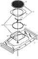
도 2는 도 1에 도시된 반응 챔버의 측단면도이다.
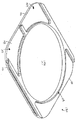
도 3은 종래 기술에 일반적으로 알려진 서셉터 링의 저부 평면도이다.
도 4는 일 실시예에 따른 자가 중심설정 서셉터 링 조립체를 구비한 반응 챔버의 측단면도이다.
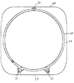
도 5는 도 4에 도시된 반응 챔버의 상부 평면도이다.
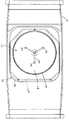
도 6a는 서셉터 링 지지 부재의 일 실시예의 상부 평면도이다.
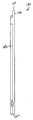
도 6b는 도 6a에 도시된 서셉터 링 지지 부재의 측면 입면도이다.
도 7a는 서셉터 링의 예시적 실시예의 저부 등각도이다.
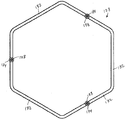
도 7b는 도 7a에 도시된 서셉터 링의 저부 평면도이다.
도 7c는 도 7a에 도시된 서셉터 링의 측면 입면도이다.
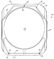
도 8은 자가 중심설정 서셉터 링 조립체의 일 실시예의 저부 평면도이다.
Claims (18)
- 반응 챔버;
적어도 부분적으로 상기 반응 챔버 내에 배치되는 서셉터를 포함하는 기판 지지 조립체; 및
상기 반응 챔버 내에 위치된 자가 중심설정 서셉터 링 조립체;
를 포함하고, 상기 자가 중심설정 서셉터 링 조립체는,
상기 반응 챔버의 하부 표면에 작동식으로 연결된 서셉터 링 지지 부재로서, 상기 반응 챔버의 상기 하부 표면으로부터 멀어지는 방향으로 돌출하는 적어도 세 개의 핀들을 포함하는 서셉터 링 지지 부재; 및
상기 서셉터 링 지지 부재 상에 지지될 수 있는 서셉터 링;
을 포함하고,
상기 서셉터 링은:
상기 서셉터 링이 상기 서셉터를 둘러싸는 것을 허용하도록 구성되고 상기 서셉터 링 내에 형성된 개구;
상기 서셉터 링의 저부 표면에 형성된 적어도 세 개의 디텐트들로서, 상기 디텐트들 각각은 상기 적어도 세 개의 핀들 중 하나를 수용하도록 구성된 디텐트들;
선단 에지 및 후단 에지를 포함하는 직사각형 외부 둘레; 및
상부 표면 및 상기 상부 표면과 상기 하부 표면 사이에서 정의된 두께;
를 포함하고,
상기 핀들은 상기 서셉터 링과 상기 서셉터 링 지지 부재가 열 팽창 및 수축할 때 상기 디텐트들 내에서 활주할 수 있어서 상기 기판 지지 조립체를 상기 자가 중심설정 서셉터 링 조립체 내에 중심설정된 상태로 유지하고,
상기 디텐트들 각각은 상기 기판 지지 조립체의 중심점에 대하여 방사상 경로를 형성하는 세장형 슬롯을 포함하고,
상기 디텐트들은 상기 개구 둘레에서 균등하게 이격되고,
상기 개구는 중심점을 가지며 상기 두께를 통하여 형성되고, 상기 개구의 상기 중심점이 상기 후단 에지보다 상기 선단 에지에 가깝게 위치하도록 상기 개구가 비대칭적으로 위치하는 반도체 처리 시스템. - 제 1 항에 있어서,
상기 서셉터 링과 상기 서셉터 링 지지 부재는 상이한 재료로 형성된 것을 특징으로 하는 반도체 처리 시스템. - 제 2 항에 있어서,
상기 서셉터 링은 그라파이트로 형성되고, 상기 서셉터 링 지지 부재는 석영으로 형성된 자가 중심설정 서셉터 링 조립체. - 제 1 항에 있어서,
상기 핀들 각각은 상기 서셉터 링의 열 팽창 및 수축 동안 독립적으로 활주할 수 있는 것을 특징으로 하는 반도체 처리 시스템. - 제 1 항에 있어서,
상기 개구는 상기 서셉터와 상기 개구를 정의하는 상기 서셉터 링의 에지 사이에 균일한 간극을 제공하도록 구성된 것을 특징으로 하는 반도체 처리 시스템. - 제 1 항에 있어서,
상기 서셉터 링 지지 부재는 상기 서셉터 링 지지 부재의 하부 표면으로부터 연장되는 하나 이상의 위치설정 부재들을 포함하고,
각 위치설정 부재는 상기 반응 챔버의 하부 표면의 대응되는 오목부 내에 수용되도록 구성된 하부 부분을 포함하는 것을 특징으로 하는 반도체 처리 시스템. - 제 1 항에 있어서,
상기 적어도 세 개의 디텐트들 중 적어도 하나는 상기 서셉터 링의 전체 두께를 관통하여 형성된 것을 특징으로 하는 반도체 처리 시스템. - 반도체 처리 툴에 사용하기 위한 자가 중심설정 서셉터 링 조립체로서,
반응 챔버의 하부 표면에 작동식으로 연결되도록 구성된 서셉터 링 지지부로서, 상기 서셉터 링 지지부는 상기 반응 챔버 내에 제공되고, 적어도 하나의 측부 부재로부터 동일한 방향으로 연장하는 적어도 세 개의 핀들을 가지며, 상기 적어도 세 개의 핀들 각각의 팁은 평면형 지지부를 형성하는 서셉터 링 지지부;
서셉터 링으로서,
상기 서셉터 링이 서셉터를 둘러싸는 것을 허용하도록 구성되고 상기 서셉터 링 내에 형성되는 개구;
적어도 세 개의 디텐트들;
선단 에지 및 후단 에지를 포함하는 직사각형 외부 둘레; 및
사이에 두께를 정의하는 상부 표면 및 하부 표면;
을 포함하는 서셉터 링;
을 포함하고,
상기 적어도 세 개의 핀들을 수용하기 위해 상기 서셉터 링 내에 형성되는 상기 적어도 세 개의 디텐트들을 구비하여 상기 서셉터 링의 열 팽창 및 수축 동안 상기 서셉터 링의 열 팽창 또는 수축이 상기 핀들이 상기 디텐트들 내에서 상대적 위치가 변화하게 하여 상기 서셉터 링이 중심점을 중심으로 중심설정된 상태를 유지할 수 있게 하고, 상기 디텐트들의 각각은 상기 중심점에 대해 방사상 방식으로 정렬된 세장형 슬롯을 포함하고 상기 디텐트들은 상기 개구 둘레에서 균등하게 이격되고,
상기 개구는 중심점을 가지며 상기 두께를 통하여 형성되고, 상기 개구의 상기 중심점이 상기 후단 에지보다 상기 선단 에지에 가깝게 위치하도록 상기 개구가 비대칭적으로 위치하는 것을 특징으로 하는 자가 중심설정 서셉터 링 조립체. - 제 8 항에 있어서,
상기 개구는 상기 서셉터와 상기 개구를 정의하는 상기 서셉터 링의 에지 사이에 균일한 간극을 제공하도록 구성되는 것을 특징으로 하는 자가 중심설정 서셉터 링 조립체. - 제 9 항에 있어서,
상기 서셉터 링의 열 팽창 및 수축 동안 상기 디텐트들 내에서의 상기 핀들의 상대적 위치의 상기 변화는 상기 서셉터와 상기 개구를 정의하는 상기 서셉터 링의 상기 에지 사이의 상기 간극이 균일하게 유지되게 하는 것을 특징으로 하는 자가 중심설정 서셉터 링 조립체. - 제 8 항에 있어서,
상기 서셉터 링과 상기 서셉터 링 지지부는 상이한 재료로 형성된 것을 특징으로 하는 자가 중심설정 서셉터 링 조립체. - 제 11 항에 있어서,
상기 서셉터 링은 그라파이트로 형성되고, 상기 서셉터 링 지지부는 석영으로 형성된 자가 중심설정 서셉터 링 조립체. - 제 8 항에 있어서,
상기 적어도 세 개의 디텐트들 중 적어도 하나는 상기 서셉터 링의 전체 두께를 관통하여 형성된 것을 특징으로 하는 자가 중심설정 서셉터 링 조립체. - 제 8 항에 있어서,
상기 서셉터 링 지지부는 상기 서셉터 링 지지부의 하부 표면으로부터 연장되는 하나 이상의 위치설정 부재들을 포함하고,
각 위치설정 부재는 반응 챔버의 하부 표면의 대응되는 오목부 내에 수용되도록 구성된 하부 부분을 포함하는 것을 특징으로 하는 자가 중심설정 서셉터 링 조립체. - 자가 중심설정 서셉터 링 조립체 내에서 적어도 세 개의 핀들을 갖는 서셉터 링 조립체와 사용하도록 구성된 서셉터 링으로서,
사이에 두께를 정의하는 상부 표면 및 하부 표면;
상기 두께를 관통하여 형성되고, 서셉터를 둘러싸도록 구성되고, 중심점을 갖는 개구;
상기 하부 표면의 내부로 형성된 적어도 세 개의 디텐트들; 및
선단 에지 및 후단 에지를 포함하는 직사각형 외부 둘레;
를 포함하고,
상기 디텐트들은 상기 중심점에 대해 방사상으로 정렬된 세장형 슬롯들이며 상기 적어도 세 개의 핀들 중 하나에 의하여 지지되도록 각각 구성되고, 상기 적어도 세 개의 디텐트들 중 하나는 상기 적어도 세 개의 디텐트들 중 다른 것보다 상기 개구의 중심점에 더 가깝고, 상기 서셉터 링의 열 팽창 또는 수축이 상기 핀들에 대한 상기 디텐트들의 상대적인 위치의 변화를 야기하고, 상기 적어도 세 개의 디텐트들 중 적어도 하나는 전체 두께를 관통하여 형성되고, 상기 디텐트들은 상기 개구 둘레에서 균등하게 이격되고,
상기 개구의 상기 중심점이 상기 후단 에지보다 상기 선단 에지에 가깝게 위치하도록 상기 개구가 비대칭적으로 위치하는 서셉터 링. - 제 15 항에 있어서,
상기 하부 표면의 내부로 전체 두께를 관통하여 형성된 세 개보다 많은 디텐트들을 더 포함하는 것을 특징으로 하는 서셉터 링. - 제 15 항에 있어서,
상기 적어도 세 개의 디텐트들 중 적어도 하나는 상기 두께의 단지 일부만을 관통하여 형성된 것을 특징으로 하는 서셉터 링. - 제 15 항에 있어서,
상기 개구는 상기 서셉터와 상기 개구를 정의하는 상기 서셉터 링의 에지 사이에 균일한 간극을 제공하도록 구성된 것을 특징으로 하는 서셉터 링.
Applications Claiming Priority (3)
| Application Number | Priority Date | Filing Date | Title |
|---|---|---|---|
| US12/263,345 | 2008-10-31 | ||
| US12/263,345 US8801857B2 (en) | 2008-10-31 | 2008-10-31 | Self-centering susceptor ring assembly |
| PCT/US2009/059501 WO2010062476A1 (en) | 2008-10-31 | 2009-10-05 | Self-centering susceptor ring assembly |
Related Parent Applications (1)
| Application Number | Title | Priority Date | Filing Date |
|---|---|---|---|
| KR1020177022993A Division KR20170098331A (ko) | 2008-10-31 | 2009-10-05 | 자가 중심설정 서셉터 링 조립체 |
Publications (2)
| Publication Number | Publication Date |
|---|---|
| KR20180098704A true KR20180098704A (ko) | 2018-09-04 |
| KR102071681B1 KR102071681B1 (ko) | 2020-01-30 |
Family
ID=42129902
Family Applications (4)
| Application Number | Title | Priority Date | Filing Date |
|---|---|---|---|
| KR1020187024675A Active KR102071681B1 (ko) | 2008-10-31 | 2009-10-05 | 자가 중심설정 서셉터 링 조립체 |
| KR1020117011976A Ceased KR20110084271A (ko) | 2008-10-31 | 2009-10-05 | 자가 중심설정 서셉터 링 조립체 |
| KR1020177022993A Ceased KR20170098331A (ko) | 2008-10-31 | 2009-10-05 | 자가 중심설정 서셉터 링 조립체 |
| KR1020167007742A Ceased KR20160040720A (ko) | 2008-10-31 | 2009-10-05 | 자가 중심설정 서셉터 링 조립체 |
Family Applications After (3)
| Application Number | Title | Priority Date | Filing Date |
|---|---|---|---|
| KR1020117011976A Ceased KR20110084271A (ko) | 2008-10-31 | 2009-10-05 | 자가 중심설정 서셉터 링 조립체 |
| KR1020177022993A Ceased KR20170098331A (ko) | 2008-10-31 | 2009-10-05 | 자가 중심설정 서셉터 링 조립체 |
| KR1020167007742A Ceased KR20160040720A (ko) | 2008-10-31 | 2009-10-05 | 자가 중심설정 서셉터 링 조립체 |
Country Status (4)
| Country | Link |
|---|---|
| US (2) | US8801857B2 (ko) |
| KR (4) | KR102071681B1 (ko) |
| CN (1) | CN102197471B (ko) |
| WO (1) | WO2010062476A1 (ko) |
Families Citing this family (18)
| Publication number | Priority date | Publication date | Assignee | Title |
|---|---|---|---|---|
| CN103132051B (zh) * | 2011-11-23 | 2015-07-08 | 中微半导体设备(上海)有限公司 | 化学气相沉积反应器或外延层生长反应器及其支撑装置 |
| KR101361711B1 (ko) * | 2011-12-30 | 2014-02-12 | 엘아이지에이디피 주식회사 | 공정챔버의 지지유닛 및 이를 포함하는 기판처리장치 |
| WO2016007253A1 (en) * | 2014-07-10 | 2016-01-14 | Applied Materials, Inc. | Design of susceptor in chemical vapor deposition reactor |
| JP1648519S (ko) * | 2018-10-04 | 2019-12-23 | ||
| USD914620S1 (en) | 2019-01-17 | 2021-03-30 | Asm Ip Holding B.V. | Vented susceptor |
| USD920936S1 (en) | 2019-01-17 | 2021-06-01 | Asm Ip Holding B.V. | Higher temperature vented susceptor |
| US11961756B2 (en) | 2019-01-17 | 2024-04-16 | Asm Ip Holding B.V. | Vented susceptor |
| CN109930132B (zh) * | 2019-03-08 | 2021-06-18 | 拓荆科技股份有限公司 | 陶瓷环及具有陶瓷环的半导体反应腔体 |
| TWI845682B (zh) | 2019-05-22 | 2024-06-21 | 荷蘭商Asm Ip私人控股有限公司 | 工件基座主體 |
| US11764101B2 (en) | 2019-10-24 | 2023-09-19 | ASM IP Holding, B.V. | Susceptor for semiconductor substrate processing |
| TWI888578B (zh) | 2020-06-23 | 2025-07-01 | 荷蘭商Asm Ip私人控股有限公司 | 基座及反應腔室 |
| CN112030130B (zh) * | 2020-08-27 | 2023-06-13 | 上海华力集成电路制造有限公司 | 定位结构及其定位方法 |
| USD1031676S1 (en) | 2020-12-04 | 2024-06-18 | Asm Ip Holding B.V. | Combined susceptor, support, and lift system |
| US12394659B2 (en) | 2021-04-30 | 2025-08-19 | Asm Ip Holding B.V. | Susceptors with film deposition control features |
| TW202314034A (zh) | 2021-06-30 | 2023-04-01 | 荷蘭商Asm Ip私人控股有限公司 | 化學氣相沉積系統及其組合 |
| USD997894S1 (en) * | 2021-09-28 | 2023-09-05 | Applied Materials, Inc. | Shadow ring lift assembly |
| USD997893S1 (en) * | 2021-09-28 | 2023-09-05 | Applied Materials, Inc. | Shadow ring lift plate |
| CN116904953A (zh) * | 2023-09-14 | 2023-10-20 | 上海陛通半导体能源科技股份有限公司 | 一种气相沉积设备 |
Citations (4)
| Publication number | Priority date | Publication date | Assignee | Title |
|---|---|---|---|---|
| KR20010012685A (ko) * | 1997-05-20 | 2001-02-26 | 히가시 데쓰로 | 처리 장치 |
| KR20010062301A (ko) * | 1999-12-10 | 2001-07-07 | 조셉 제이. 스위니 | 자가 정렬 비접촉식 섀도우 링 공정 키트 |
| US6325858B1 (en) * | 1997-11-03 | 2001-12-04 | Asm America, Inc. | Long life high temperature process chamber |
| KR100660416B1 (ko) * | 1997-11-03 | 2006-12-22 | 에이에스엠 아메리카, 인코포레이티드 | 개량된 저질량 웨이퍼 지지 시스템 |
Family Cites Families (70)
| Publication number | Priority date | Publication date | Assignee | Title |
|---|---|---|---|---|
| US3407783A (en) * | 1964-08-31 | 1968-10-29 | Emil R. Capita | Vapor deposition apparatus |
| US3549847A (en) * | 1967-04-18 | 1970-12-22 | Gen Electric | Graphite susceptor |
| JPS4930319B1 (ko) * | 1969-08-29 | 1974-08-12 | ||
| US4522149A (en) * | 1983-11-21 | 1985-06-11 | General Instrument Corp. | Reactor and susceptor for chemical vapor deposition process |
| US4560420A (en) * | 1984-06-13 | 1985-12-24 | At&T Technologies, Inc. | Method for reducing temperature variations across a semiconductor wafer during heating |
| JPS6169116A (ja) * | 1984-09-13 | 1986-04-09 | Toshiba Ceramics Co Ltd | シリコンウエハ−の連続cvdコ−テイング用サセプター |
| NL8602356A (nl) | 1985-10-07 | 1987-05-04 | Epsilon Ltd Partnership | Inrichting en werkwijze voor een axiaal symmetrische reactor voor het chemische uit damp neerslaan. |
| US5200157A (en) * | 1986-02-17 | 1993-04-06 | Toshiba Ceramics Co., Ltd. | Susceptor for vapor-growth deposition |
| US5000113A (en) * | 1986-12-19 | 1991-03-19 | Applied Materials, Inc. | Thermal CVD/PECVD reactor and use for thermal chemical vapor deposition of silicon dioxide and in-situ multi-step planarized process |
| JPS63186422A (ja) * | 1987-01-28 | 1988-08-02 | Tadahiro Omi | ウエハサセプタ装置 |
| US4821674A (en) * | 1987-03-31 | 1989-04-18 | Deboer Wiebe B | Rotatable substrate supporting mechanism with temperature sensing device for use in chemical vapor deposition equipment |
| US4978567A (en) | 1988-03-31 | 1990-12-18 | Materials Technology Corporation, Subsidiary Of The Carbon/Graphite Group, Inc. | Wafer holding fixture for chemical reaction processes in rapid thermal processing equipment and method for making same |
| KR0155545B1 (ko) * | 1988-06-27 | 1998-12-01 | 고다까 토시오 | 기판의 열처리 장치 |
| US5306699A (en) * | 1988-08-31 | 1994-04-26 | Superconductor Technologies, Inc. | Reactor vessel for manufacture of superconducting films |
| JP2731855B2 (ja) * | 1989-02-14 | 1998-03-25 | アネルバ株式会社 | 減圧気相成長装置 |
| US5156820A (en) * | 1989-05-15 | 1992-10-20 | Rapro Technology, Inc. | Reaction chamber with controlled radiant energy heating and distributed reactant flow |
| US5119540A (en) * | 1990-07-24 | 1992-06-09 | Cree Research, Inc. | Apparatus for eliminating residual nitrogen contamination in epitaxial layers of silicon carbide and resulting product |
| US4990374A (en) * | 1989-11-28 | 1991-02-05 | Cvd Incorporated | Selective area chemical vapor deposition |
| US5108792A (en) * | 1990-03-09 | 1992-04-28 | Applied Materials, Inc. | Double-dome reactor for semiconductor processing |
| EP0448346B1 (en) | 1990-03-19 | 1997-07-09 | Kabushiki Kaisha Toshiba | Vapor-phase deposition apparatus |
| US5098198A (en) * | 1990-04-19 | 1992-03-24 | Applied Materials, Inc. | Wafer heating and monitor module and method of operation |
| US5094885A (en) * | 1990-10-12 | 1992-03-10 | Genus, Inc. | Differential pressure cvd chuck |
| US5121531A (en) * | 1990-07-06 | 1992-06-16 | Applied Materials, Inc. | Refractory susceptors for epitaxial deposition apparatus |
| US5620525A (en) * | 1990-07-16 | 1997-04-15 | Novellus Systems, Inc. | Apparatus for supporting a substrate and introducing gas flow doximate to an edge of the substrate |
| US5044943A (en) * | 1990-08-16 | 1991-09-03 | Applied Materials, Inc. | Spoked susceptor support for enhanced thermal uniformity of susceptor in semiconductor wafer processing apparatus |
| US5298465A (en) * | 1990-08-16 | 1994-03-29 | Applied Materials, Inc. | Plasma etching system |
| US5304248A (en) * | 1990-12-05 | 1994-04-19 | Applied Materials, Inc. | Passive shield for CVD wafer processing which provides frontside edge exclusion and prevents backside depositions |
| US5356486A (en) * | 1991-03-04 | 1994-10-18 | Applied Materials, Inc. | Combined wafer support and temperature monitoring device |
| US5199483A (en) * | 1991-05-15 | 1993-04-06 | Applied Materials, Inc. | Method and apparatus for cooling wafers |
| US5393349A (en) * | 1991-08-16 | 1995-02-28 | Tokyo Electron Sagami Kabushiki Kaisha | Semiconductor wafer processing apparatus |
| US5332442A (en) * | 1991-11-15 | 1994-07-26 | Tokyo Electron Kabushiki Kaisha | Surface processing apparatus |
| US5370739A (en) * | 1992-06-15 | 1994-12-06 | Materials Research Corporation | Rotating susceptor semiconductor wafer processing cluster tool module useful for tungsten CVD |
| US5308645A (en) * | 1992-08-07 | 1994-05-03 | Delco Electronics Corporation | Method and apparatus for through hole substrate printing |
| US5803977A (en) * | 1992-09-30 | 1998-09-08 | Applied Materials, Inc. | Apparatus for full wafer deposition |
| US5343938A (en) * | 1992-12-24 | 1994-09-06 | Vlsi Technology, Inc. | Method and apparatus for thermally insulating a wafer support |
| DE69331659T2 (de) * | 1993-01-13 | 2002-09-12 | Applied Materials Inc | Verfahren zur Abscheidung von Polysiliziumschichten mit einer verbesserten Uniformität und dazugehörige Vorrichtung |
| US5444217A (en) * | 1993-01-21 | 1995-08-22 | Moore Epitaxial Inc. | Rapid thermal processing apparatus for processing semiconductor wafers |
| EP0611273B1 (de) * | 1993-02-08 | 1998-09-16 | SEZ Semiconductor-Equipment Zubehör für die Halbleiterfertigung AG | Träger für scheibenförmige Gegenstände |
| US5421893A (en) * | 1993-02-26 | 1995-06-06 | Applied Materials, Inc. | Susceptor drive and wafer displacement mechanism |
| NL9300389A (nl) * | 1993-03-04 | 1994-10-03 | Xycarb Bv | Substraatdrager. |
| US5738165A (en) * | 1993-05-07 | 1998-04-14 | Nikon Corporation | Substrate holding apparatus |
| JPH0711446A (ja) * | 1993-05-27 | 1995-01-13 | Applied Materials Inc | 気相成長用サセプタ装置 |
| DE69404397T2 (de) | 1993-07-13 | 1997-11-13 | Applied Materials Inc | Verbesserte Suszeptor Ausführung |
| JPH0758039A (ja) | 1993-08-20 | 1995-03-03 | Toshiba Ceramics Co Ltd | サセプタ |
| US5549756A (en) * | 1994-02-02 | 1996-08-27 | Applied Materials, Inc. | Optical pyrometer for a thin film deposition system |
| US5467220A (en) * | 1994-02-18 | 1995-11-14 | Applied Materials, Inc. | Method and apparatus for improving semiconductor wafer surface temperature uniformity |
| US6033480A (en) * | 1994-02-23 | 2000-03-07 | Applied Materials, Inc. | Wafer edge deposition elimination |
| US5645646A (en) * | 1994-02-25 | 1997-07-08 | Applied Materials, Inc. | Susceptor for deposition apparatus |
| EP0669640A1 (en) | 1994-02-25 | 1995-08-30 | Applied Materials, Inc. | Susceptor for deposition apparatus |
| US5514439A (en) * | 1994-10-14 | 1996-05-07 | Sibley; Thomas | Wafer support fixtures for rapid thermal processing |
| US5558717A (en) * | 1994-11-30 | 1996-09-24 | Applied Materials | CVD Processing chamber |
| NL9500614A (nl) * | 1995-03-30 | 1996-11-01 | Helpman Intellectual Propertie | Warmtewisselaar. |
| JP3028462B2 (ja) * | 1995-05-12 | 2000-04-04 | 東京エレクトロン株式会社 | 熱処理装置 |
| FR2735238B1 (fr) * | 1995-06-09 | 1997-09-05 | Cis Bio Int | Utilisation d'un complexe phycobiliproteine-peptide de liaison en tant que traceur fluorescent |
| US5700725A (en) * | 1995-06-26 | 1997-12-23 | Lucent Technologies Inc. | Apparatus and method for making integrated circuits |
| US6093252A (en) * | 1995-08-03 | 2000-07-25 | Asm America, Inc. | Process chamber with inner support |
| JP3430277B2 (ja) * | 1995-08-04 | 2003-07-28 | 東京エレクトロン株式会社 | 枚葉式の熱処理装置 |
| US5551985A (en) * | 1995-08-18 | 1996-09-03 | Torrex Equipment Corporation | Method and apparatus for cold wall chemical vapor deposition |
| US6086680A (en) | 1995-08-22 | 2000-07-11 | Asm America, Inc. | Low-mass susceptor |
| JPH09181155A (ja) | 1995-09-29 | 1997-07-11 | Applied Materials Inc | 堆積装置のサセプタ |
| US5584936A (en) * | 1995-12-14 | 1996-12-17 | Cvd, Incorporated | Susceptor for semiconductor wafer processing |
| US5656093A (en) * | 1996-03-08 | 1997-08-12 | Applied Materials, Inc. | Wafer spacing mask for a substrate support chuck and method of fabricating same |
| US6395363B1 (en) | 1996-11-05 | 2002-05-28 | Applied Materials, Inc. | Sloped substrate support |
| US6090212A (en) * | 1997-08-15 | 2000-07-18 | Micro C Technologies, Inc. | Substrate platform for a semiconductor substrate during rapid high temperature processing and method of supporting a substrate |
| US6293749B1 (en) * | 1997-11-21 | 2001-09-25 | Asm America, Inc. | Substrate transfer system for semiconductor processing equipment |
| US6219219B1 (en) | 1998-09-30 | 2001-04-17 | Applied Materials, Inc. | Cathode assembly containing an electrostatic chuck for retaining a wafer in a semiconductor wafer processing system |
| JP2000269310A (ja) | 1999-03-15 | 2000-09-29 | Toshiba Corp | 半導体ウェハ支持装置 |
| JP2002184843A (ja) | 2000-12-13 | 2002-06-28 | Sharp Corp | 半導体基板保持装置 |
| KR20070098025A (ko) | 2006-03-30 | 2007-10-05 | 삼성전자주식회사 | 반도체 소자 제조용 장비 |
| US8394229B2 (en) * | 2008-08-07 | 2013-03-12 | Asm America, Inc. | Susceptor ring |
-
2008
- 2008-10-31 US US12/263,345 patent/US8801857B2/en active Active
-
2009
- 2009-10-05 KR KR1020187024675A patent/KR102071681B1/ko active Active
- 2009-10-05 CN CN2009801426742A patent/CN102197471B/zh active Active
- 2009-10-05 KR KR1020117011976A patent/KR20110084271A/ko not_active Ceased
- 2009-10-05 WO PCT/US2009/059501 patent/WO2010062476A1/en not_active Ceased
- 2009-10-05 KR KR1020177022993A patent/KR20170098331A/ko not_active Ceased
- 2009-10-05 KR KR1020167007742A patent/KR20160040720A/ko not_active Ceased
-
2014
- 2014-07-30 US US14/447,383 patent/US11387137B2/en active Active
Patent Citations (4)
| Publication number | Priority date | Publication date | Assignee | Title |
|---|---|---|---|---|
| KR20010012685A (ko) * | 1997-05-20 | 2001-02-26 | 히가시 데쓰로 | 처리 장치 |
| US6325858B1 (en) * | 1997-11-03 | 2001-12-04 | Asm America, Inc. | Long life high temperature process chamber |
| KR100660416B1 (ko) * | 1997-11-03 | 2006-12-22 | 에이에스엠 아메리카, 인코포레이티드 | 개량된 저질량 웨이퍼 지지 시스템 |
| KR20010062301A (ko) * | 1999-12-10 | 2001-07-07 | 조셉 제이. 스위니 | 자가 정렬 비접촉식 섀도우 링 공정 키트 |
Also Published As
| Publication number | Publication date |
|---|---|
| CN102197471A (zh) | 2011-09-21 |
| CN102197471B (zh) | 2013-08-21 |
| US8801857B2 (en) | 2014-08-12 |
| KR102071681B1 (ko) | 2020-01-30 |
| KR20110084271A (ko) | 2011-07-21 |
| WO2010062476A1 (en) | 2010-06-03 |
| US11387137B2 (en) | 2022-07-12 |
| US20100107973A1 (en) | 2010-05-06 |
| KR20160040720A (ko) | 2016-04-14 |
| KR20170098331A (ko) | 2017-08-29 |
| US20140338596A1 (en) | 2014-11-20 |
Similar Documents
| Publication | Publication Date | Title |
|---|---|---|
| KR20180098704A (ko) | 자가 중심설정 서셉터 링 조립체 | |
| US8394229B2 (en) | Susceptor ring | |
| TWI839443B (zh) | 通風基座 | |
| US7601224B2 (en) | Method of supporting a substrate in a gas cushion susceptor system | |
| CN107112265B (zh) | 基板传送机构 | |
| KR102615853B1 (ko) | 기판 캐리어 시스템 | |
| KR100893909B1 (ko) | 기판 홀더의 제조 방법 | |
| KR102283740B1 (ko) | 에피택시 반응기에서의 반도체 웨이퍼를 취급하는 장치 및 에피택셜 층을 갖는 반도체 웨이퍼를 제조하는 방법 | |
| KR20070091332A (ko) | 웨이퍼 지지핀 어셈블리 | |
| CN106463450A (zh) | 在epi腔室中的基板热控制 | |
| JP4637475B2 (ja) | 取外し可能なサセプタを用いた半導体基板搬送システム、及び半導体基板の搬送方法 | |
| CN113508452B (zh) | 气相沉积装置及外延硅晶片的制造方法 | |
| CN107460451B (zh) | 自居中底座加热器 | |
| US20220172980A1 (en) | Self-centering susceptor ring assembly | |
| US11004704B2 (en) | Finned rotor cover | |
| CN115274526A (zh) | 具有定心功能的基板载体 |
Legal Events
| Date | Code | Title | Description |
|---|---|---|---|
| A107 | Divisional application of patent | ||
| A201 | Request for examination | ||
| PA0104 | Divisional application for international application |
St.27 status event code: A-0-1-A10-A18-div-PA0104 St.27 status event code: A-0-1-A10-A16-div-PA0104 |
|
| PA0201 | Request for examination |
St.27 status event code: A-1-2-D10-D11-exm-PA0201 |
|
| PG1501 | Laying open of application |
St.27 status event code: A-1-1-Q10-Q12-nap-PG1501 |
|
| E902 | Notification of reason for refusal | ||
| PE0902 | Notice of grounds for rejection |
St.27 status event code: A-1-2-D10-D21-exm-PE0902 |
|
| T11-X000 | Administrative time limit extension requested |
St.27 status event code: U-3-3-T10-T11-oth-X000 |
|
| AMND | Amendment | ||
| E13-X000 | Pre-grant limitation requested |
St.27 status event code: A-2-3-E10-E13-lim-X000 |
|
| P11-X000 | Amendment of application requested |
St.27 status event code: A-2-2-P10-P11-nap-X000 |
|
| P13-X000 | Application amended |
St.27 status event code: A-2-2-P10-P13-nap-X000 |
|
| E601 | Decision to refuse application | ||
| PE0601 | Decision on rejection of patent |
St.27 status event code: N-2-6-B10-B15-exm-PE0601 |
|
| X091 | Application refused [patent] | ||
| T11-X000 | Administrative time limit extension requested |
St.27 status event code: U-3-3-T10-T11-oth-X000 |
|
| T13-X000 | Administrative time limit extension granted |
St.27 status event code: U-3-3-T10-T13-oth-X000 |
|
| T11-X000 | Administrative time limit extension requested |
St.27 status event code: U-3-3-T10-T11-oth-X000 |
|
| T13-X000 | Administrative time limit extension granted |
St.27 status event code: U-3-3-T10-T13-oth-X000 |
|
| AMND | Amendment | ||
| E13-X000 | Pre-grant limitation requested |
St.27 status event code: A-2-3-E10-E13-lim-X000 |
|
| P11-X000 | Amendment of application requested |
St.27 status event code: A-2-2-P10-P11-nap-X000 |
|
| P13-X000 | Application amended |
St.27 status event code: A-2-2-P10-P13-nap-X000 |
|
| PX0901 | Re-examination |
St.27 status event code: A-2-3-E10-E12-rex-PX0901 |
|
| E90F | Notification of reason for final refusal | ||
| PE0902 | Notice of grounds for rejection |
St.27 status event code: A-1-2-D10-D21-exm-PE0902 |
|
| AMND | Amendment | ||
| P11-X000 | Amendment of application requested |
St.27 status event code: A-2-2-P10-P11-nap-X000 |
|
| P13-X000 | Application amended |
St.27 status event code: A-2-2-P10-P13-nap-X000 |
|
| PX0701 | Decision of registration after re-examination |
St.27 status event code: A-3-4-F10-F13-rex-PX0701 |
|
| X701 | Decision to grant (after re-examination) | ||
| GRNT | Written decision to grant | ||
| PR0701 | Registration of establishment |
St.27 status event code: A-2-4-F10-F11-exm-PR0701 |
|
| PR1002 | Payment of registration fee |
St.27 status event code: A-2-2-U10-U12-oth-PR1002 Fee payment year number: 1 |
|
| PG1601 | Publication of registration |
St.27 status event code: A-4-4-Q10-Q13-nap-PG1601 |
|
| PN2301 | Change of applicant |
St.27 status event code: A-5-5-R10-R11-asn-PN2301 |
|
| PN2301 | Change of applicant |
St.27 status event code: A-5-5-R10-R14-asn-PN2301 |
|
| PR1001 | Payment of annual fee |
St.27 status event code: A-4-4-U10-U11-oth-PR1001 Fee payment year number: 4 |
|
| PR1001 | Payment of annual fee |
St.27 status event code: A-4-4-U10-U11-oth-PR1001 Fee payment year number: 5 |
|
| PR1001 | Payment of annual fee |
St.27 status event code: A-4-4-U10-U11-oth-PR1001 Fee payment year number: 6 |
|
| P22-X000 | Classification modified |
St.27 status event code: A-4-4-P10-P22-nap-X000 |