KR20180098448A - 잔류 가스 제거 장치 및 이를 포함하는 기판 처리 설비 - Google Patents
잔류 가스 제거 장치 및 이를 포함하는 기판 처리 설비 Download PDFInfo
- Publication number
- KR20180098448A KR20180098448A KR1020170024955A KR20170024955A KR20180098448A KR 20180098448 A KR20180098448 A KR 20180098448A KR 1020170024955 A KR1020170024955 A KR 1020170024955A KR 20170024955 A KR20170024955 A KR 20170024955A KR 20180098448 A KR20180098448 A KR 20180098448A
- Authority
- KR
- South Korea
- Prior art keywords
- substrate
- housing
- unit
- gas
- support member
- Prior art date
- Legal status (The legal status is an assumption and is not a legal conclusion. Google has not performed a legal analysis and makes no representation as to the accuracy of the status listed.)
- Granted
Links
Images


Classifications
-
- H—ELECTRICITY
- H10—SEMICONDUCTOR DEVICES; ELECTRIC SOLID-STATE DEVICES NOT OTHERWISE PROVIDED FOR
- H10P—GENERIC PROCESSES OR APPARATUS FOR THE MANUFACTURE OR TREATMENT OF DEVICES COVERED BY CLASS H10
- H10P72/00—Handling or holding of wafers, substrates or devices during manufacture or treatment thereof
- H10P72/04—Apparatus for manufacture or treatment
- H10P72/0402—Apparatus for fluid treatment
- H10P72/0406—Apparatus for fluid treatment for cleaning followed by drying, rinsing, stripping, blasting or the like
- H10P72/0408—Apparatus for fluid treatment for cleaning followed by drying, rinsing, stripping, blasting or the like for drying
-
- H—ELECTRICITY
- H10—SEMICONDUCTOR DEVICES; ELECTRIC SOLID-STATE DEVICES NOT OTHERWISE PROVIDED FOR
- H10P—GENERIC PROCESSES OR APPARATUS FOR THE MANUFACTURE OR TREATMENT OF DEVICES COVERED BY CLASS H10
- H10P70/00—Cleaning of wafers, substrates or parts of devices
- H10P70/10—Cleaning before device manufacture, i.e. Begin-Of-Line process
- H10P70/12—Cleaning before device manufacture, i.e. Begin-Of-Line process by dry cleaning only
-
- H01L21/02046—
-
- B—PERFORMING OPERATIONS; TRANSPORTING
- B08—CLEANING
- B08B—CLEANING IN GENERAL; PREVENTION OF FOULING IN GENERAL
- B08B7/00—Cleaning by methods not provided for in a single other subclass or a single group in this subclass
- B08B7/0064—Cleaning by methods not provided for in a single other subclass or a single group in this subclass by temperature changes
- B08B7/0071—Cleaning by methods not provided for in a single other subclass or a single group in this subclass by temperature changes by heating
-
- H01L21/67098—
-
- H01L21/67196—
-
- H01L21/67201—
-
- H01L21/67207—
-
- H01L21/67248—
-
- H01L21/683—
-
- H—ELECTRICITY
- H10—SEMICONDUCTOR DEVICES; ELECTRIC SOLID-STATE DEVICES NOT OTHERWISE PROVIDED FOR
- H10P—GENERIC PROCESSES OR APPARATUS FOR THE MANUFACTURE OR TREATMENT OF DEVICES COVERED BY CLASS H10
- H10P72/00—Handling or holding of wafers, substrates or devices during manufacture or treatment thereof
- H10P72/04—Apparatus for manufacture or treatment
- H10P72/0402—Apparatus for fluid treatment
-
- H—ELECTRICITY
- H10—SEMICONDUCTOR DEVICES; ELECTRIC SOLID-STATE DEVICES NOT OTHERWISE PROVIDED FOR
- H10P—GENERIC PROCESSES OR APPARATUS FOR THE MANUFACTURE OR TREATMENT OF DEVICES COVERED BY CLASS H10
- H10P72/00—Handling or holding of wafers, substrates or devices during manufacture or treatment thereof
- H10P72/04—Apparatus for manufacture or treatment
- H10P72/0431—Apparatus for thermal treatment
- H10P72/0436—Apparatus for thermal treatment mainly by radiation
-
- H—ELECTRICITY
- H10—SEMICONDUCTOR DEVICES; ELECTRIC SOLID-STATE DEVICES NOT OTHERWISE PROVIDED FOR
- H10P—GENERIC PROCESSES OR APPARATUS FOR THE MANUFACTURE OR TREATMENT OF DEVICES COVERED BY CLASS H10
- H10P72/00—Handling or holding of wafers, substrates or devices during manufacture or treatment thereof
- H10P72/04—Apparatus for manufacture or treatment
- H10P72/0451—Apparatus for manufacturing or treating in a plurality of work-stations
- H10P72/0452—Apparatus for manufacturing or treating in a plurality of work-stations characterised by the layout of the process chambers
- H10P72/0454—Apparatus for manufacturing or treating in a plurality of work-stations characterised by the layout of the process chambers surrounding a central transfer chamber
-
- H—ELECTRICITY
- H10—SEMICONDUCTOR DEVICES; ELECTRIC SOLID-STATE DEVICES NOT OTHERWISE PROVIDED FOR
- H10P—GENERIC PROCESSES OR APPARATUS FOR THE MANUFACTURE OR TREATMENT OF DEVICES COVERED BY CLASS H10
- H10P72/00—Handling or holding of wafers, substrates or devices during manufacture or treatment thereof
- H10P72/04—Apparatus for manufacture or treatment
- H10P72/0451—Apparatus for manufacturing or treating in a plurality of work-stations
- H10P72/0462—Apparatus for manufacturing or treating in a plurality of work-stations characterised by the construction of the processing chambers, e.g. modular processing chambers
-
- H—ELECTRICITY
- H10—SEMICONDUCTOR DEVICES; ELECTRIC SOLID-STATE DEVICES NOT OTHERWISE PROVIDED FOR
- H10P—GENERIC PROCESSES OR APPARATUS FOR THE MANUFACTURE OR TREATMENT OF DEVICES COVERED BY CLASS H10
- H10P72/00—Handling or holding of wafers, substrates or devices during manufacture or treatment thereof
- H10P72/04—Apparatus for manufacture or treatment
- H10P72/0451—Apparatus for manufacturing or treating in a plurality of work-stations
- H10P72/0464—Apparatus for manufacturing or treating in a plurality of work-stations characterised by the construction of the transfer chamber
-
- H—ELECTRICITY
- H10—SEMICONDUCTOR DEVICES; ELECTRIC SOLID-STATE DEVICES NOT OTHERWISE PROVIDED FOR
- H10P—GENERIC PROCESSES OR APPARATUS FOR THE MANUFACTURE OR TREATMENT OF DEVICES COVERED BY CLASS H10
- H10P72/00—Handling or holding of wafers, substrates or devices during manufacture or treatment thereof
- H10P72/04—Apparatus for manufacture or treatment
- H10P72/0451—Apparatus for manufacturing or treating in a plurality of work-stations
- H10P72/0466—Apparatus for manufacturing or treating in a plurality of work-stations characterised by the construction of the load-lock chamber
-
- H—ELECTRICITY
- H10—SEMICONDUCTOR DEVICES; ELECTRIC SOLID-STATE DEVICES NOT OTHERWISE PROVIDED FOR
- H10P—GENERIC PROCESSES OR APPARATUS FOR THE MANUFACTURE OR TREATMENT OF DEVICES COVERED BY CLASS H10
- H10P72/00—Handling or holding of wafers, substrates or devices during manufacture or treatment thereof
- H10P72/04—Apparatus for manufacture or treatment
- H10P72/0451—Apparatus for manufacturing or treating in a plurality of work-stations
- H10P72/0468—Apparatus for manufacturing or treating in a plurality of work-stations comprising a chamber adapted to a particular process
-
- H—ELECTRICITY
- H10—SEMICONDUCTOR DEVICES; ELECTRIC SOLID-STATE DEVICES NOT OTHERWISE PROVIDED FOR
- H10P—GENERIC PROCESSES OR APPARATUS FOR THE MANUFACTURE OR TREATMENT OF DEVICES COVERED BY CLASS H10
- H10P72/00—Handling or holding of wafers, substrates or devices during manufacture or treatment thereof
- H10P72/06—Apparatus for monitoring, sorting, marking, testing or measuring
- H10P72/0602—Temperature monitoring
-
- H—ELECTRICITY
- H10—SEMICONDUCTOR DEVICES; ELECTRIC SOLID-STATE DEVICES NOT OTHERWISE PROVIDED FOR
- H10P—GENERIC PROCESSES OR APPARATUS FOR THE MANUFACTURE OR TREATMENT OF DEVICES COVERED BY CLASS H10
- H10P72/00—Handling or holding of wafers, substrates or devices during manufacture or treatment thereof
- H10P72/30—Handling or holding of wafers, substrates or devices during manufacture or treatment thereof for conveying, e.g. between different workstations
- H10P72/33—Handling or holding of wafers, substrates or devices during manufacture or treatment thereof for conveying, e.g. between different workstations into and out of processing chamber
- H10P72/3306—Horizontal transfer of a single workpiece
-
- H—ELECTRICITY
- H10—SEMICONDUCTOR DEVICES; ELECTRIC SOLID-STATE DEVICES NOT OTHERWISE PROVIDED FOR
- H10P—GENERIC PROCESSES OR APPARATUS FOR THE MANUFACTURE OR TREATMENT OF DEVICES COVERED BY CLASS H10
- H10P72/00—Handling or holding of wafers, substrates or devices during manufacture or treatment thereof
- H10P72/30—Handling or holding of wafers, substrates or devices during manufacture or treatment thereof for conveying, e.g. between different workstations
- H10P72/34—Handling or holding of wafers, substrates or devices during manufacture or treatment thereof for conveying, e.g. between different workstations the wafers being stored in a carrier, involving loading and unloading
- H10P72/3411—Handling or holding of wafers, substrates or devices during manufacture or treatment thereof for conveying, e.g. between different workstations the wafers being stored in a carrier, involving loading and unloading involving loading and unloading of wafers
-
- H—ELECTRICITY
- H10—SEMICONDUCTOR DEVICES; ELECTRIC SOLID-STATE DEVICES NOT OTHERWISE PROVIDED FOR
- H10P—GENERIC PROCESSES OR APPARATUS FOR THE MANUFACTURE OR TREATMENT OF DEVICES COVERED BY CLASS H10
- H10P72/00—Handling or holding of wafers, substrates or devices during manufacture or treatment thereof
- H10P72/70—Handling or holding of wafers, substrates or devices during manufacture or treatment thereof for supporting or gripping
Landscapes
- Container, Conveyance, Adherence, Positioning, Of Wafer (AREA)
- Health & Medical Sciences (AREA)
- Toxicology (AREA)
Abstract
Description
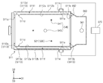
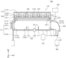
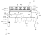
도 3은 도 1 및 도 2의 잔류 가스 제거 장치를 나타낸 사시도이다.
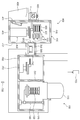
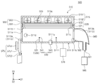
도 4는 도 3의 잔류 가스 제거 장치를 나타낸 개략도이다.
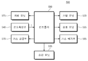
도 5는 도 3의 잔류 가스 제거 장치의 일부 구성을 나타낸 블록도이다.
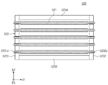
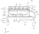
도 6은 도 3의 잔류 가스 제거 장치의 일부 구성을 나타낸 평면도이다.
도 7은 도 4의 가열 유닛을 나타낸 평면도이다.
도 8은 도 7의 가스 공급부에서 하우징 내로 비 반응성 가스가 공급되는 모습을 설명하기 위한 평면도이다.
도 9는 도 2의 기판 처리 설비 장치의 변형 예를 나타낸 개략도이다.
도 10a는 도 3의 잔류 가스 제거 장치의 변형 예를 나타낸 개략도이다.
도 10b는 도 10a의 잔류 가스 제거 장치의 일부 구성을 나타낸 블록도이다.
도 11은 도 3의 잔류 가스 제거 장치의 변형 예를 나타낸 개략도이다.
도 12 내지 도 16는 도 3의 잔류 가스 제거 장치가 기판의 잔류 가스를 제거하는 과정들을 나타낸 개략도들이다.
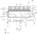
200: 트랜스퍼 챔버 250: 제1 기판 이송 유닛
300: 로드락 챔버 400: 기판 이송 모듈
410: 인덱스 챔버 450: 제2 기판 이송 유닛
500: 잔류 가스 제거 장치 510: 하우징
511: 하부 몸체 511a: 제1 개구부
511b: 제2 개구부 511d: 배출 홀
511e: 공급 홀 511f: 가스 유동 유로
5111: 바닥부 5112a: 내측면
5112b: 외측면 5113: 제1 둘레부
5113a: 제1 측벽 5113b: 제2 측벽
5113c: 제3 측벽 5113d: 제4 측벽
515: 상부 몸체 515a: 방열 홀
5151: 덮개부 5153: 제2 둘레부
520: 가열 유닛 521: 발열체
530: 지지 부재 535: 승강 유닛
5351: 승강 실린더 5353: 연결 부재
540: 온도 측정부 541: 제1 온도 측정 유닛
543: 제2 온도 측정 유닛 550: 방열 부재
555: 송풍 유닛 560: 배기 부재
565: 가스 배기부 570: 가스 공급부
573: 가스 배관 부재 575: 개폐 유닛
580: 결합 부재 590: 컨트롤러
Claims (10)
- 하우징;
상기 하우징 내로 비 반응성 가스를 공급하는 가스 공급부;
상기 하우징 내에서, 기판을 지지하도록 제공되는 지지 부재;
상기 하우징 내에서, 상기 지지 부재와 이격되는 방열 부재; 및
상기 방열 부재와 상기 지지 부재 사이에 위치되고, 상기 지지 부재를 향해 열을 제공하는 가열 유닛을 포함하는 잔류 가스 제거 장치. - 제1항에 있어서,
상기 가열 유닛은, 적어도 하나의 발열체를 포함하고,
상기 발열체는, 광을 조사하는 램프, 및 열을 발산하는 전열기 중 어느 하나인 잔류 가스 제거 장치. - 제1항에 있어서,
상기 하우징은:
상기 지지 부재를 지지하는 바닥부, 상기 바닥부와 대향되게 이격되는 덮개부, 상기 바닥부의 경계로부터 상기 덮개부를 향해 연장되는 제1 둘레부, 및 상기 덮개부의 경계로부터 상기 바닥부를 향해 연장되는 제2 둘레부를 포함하고,
상기 제1 둘레부는:
그를 관통하는 제1 개구부를 갖는 제1 측벽;
상기 제1 측벽과 대향되고, 그를 관통하는 제2 개구부를 갖는 제2 측벽;
상기 제1 및 제2 측벽들의 일측을 연결하는 제3 측벽; 및
상기 제3 측벽과 대향되고, 상기 제1 및 제2 측벽들의 타측을 연결하는 제4 측벽을 포함하는 잔류 가스 제거 장치. - 제3항에 있어서,
상기 제3 및 제4 측벽들의 각각은:
상기 제1 개구부와 인접한 배출 홀을 갖는 내측면;
상기 내측면과 대향되고, 상기 제2 개구부와 인접하며 상기 가스 공급부와 연결되는 공급 홀을 갖는 외측면; 및
상기 내측면과 상기 외측면 사이에 위치되고, 상기 배출 홀과 상기 공급 홀을 연결하는 가스 유동 유로를 갖는 잔류 가스 제거 장치. - 제1항에 있어서,
상기 하우징 내에서, 상기 방열 부재와 인접하게 위치되는 적어도 하나의 송풍 유닛을 포함하고,
상기 하우징은 상기 송풍 유닛에 의해 송풍되는 가스를 배출하는 적어도 하나의 방열 홀을 갖는 잔류 가스 제거 장치. - 제1항에 있어서,
상기 기판의 온도를 측정하도록 제공되는 온도 측정부; 및
상기 온도 측정부에서 측정한 온도 정보를 이용하여, 상기 가열 유닛을 제어하는 컨트롤러를 더 포함하는 잔류 가스 제거 장치. - 제6항에 있어서,
상기 지지 부재를 상기 가열 유닛을 향해 이동시키는 승강 유닛을 더 포함하는 잔류 가스 제거 장치. - 적어도 하나의 공정 처리 모듈;
상기 공정 처리 모듈과 이격된 로드락 챔버;
상기 공정 처리 모듈과 상기 로드락 챔버의 일측을 연결하는 트랜스퍼 챔버;
상기 로드락 챔버의 타측과 연결되는 기판 이송 모듈; 및
상기 기판 이송 모듈과 연결되는 적어도 하나의 잔류 가스 제거 장치를 포함하고,
상기 기판 이송 모듈은, 상기 로드락 챔버와 상기 잔류 가스 제거 장치 간에 기판을 이송하는 기판 이송 유닛을 포함하고,
상기 잔류 가스 제거 장치는:
하우징;
상기 하우징 내로 비 반응성 가스를 공급하는 가스 공급부;
상기 하우징 내에서, 상기 기판을 지지하도록 제공되는 지지 부재;
상기 하우징 내에서, 상기 지지 부재와 이격되는 방열 부재; 및
상기 방열 부재와 상기 지지 부재 사이에 위치되고, 상기 지지 부재를 향해 열을 제공하는 가열 유닛을 포함하는 기판 처리 설비. - 제8항에 있어서,
상기 하우징은, 상기 지지 부재를 지지하는 바닥부, 상기 바닥부와 대향되게 이격되는 덮개부, 상기 바닥부의 경계로부터 상기 덮개부를 향해 연장되는 제1 둘레부, 및 상기 덮개부의 경계로부터 상기 바닥부를 향해 연장되는 제2 둘레부를 포함하고,
상기 제1 둘레부는:
그를 관통하는 제1 개구부를 갖는 제1 측벽;
상기 제1 측벽과 대향되고, 그를 관통하는 제2 개구부를 갖는 제2 측벽;
상기 제1 및 제2 측벽들의 일측을 연결하는 제3 측벽; 및
상기 제3 측벽과 대향되고, 상기 제1 및 제2 측벽들의 타측을 연결하는 제4 측벽을 포함하는 기판 처리 설비. - 제8항에 있어서,
상기 기판의 온도를 측정하도록 제공되는 온도 측정부; 및
상기 온도 측정부에서 측정한 온도 정보를 이용하여, 상기 가열 유닛을 제어하는 가열 유닛을 더 포함하는 기판 처리 설비.
Priority Applications (2)
| Application Number | Priority Date | Filing Date | Title |
|---|---|---|---|
| KR1020170024955A KR102790075B1 (ko) | 2017-02-24 | 2017-02-24 | 잔류 가스 제거 장치 및 이를 포함하는 기판 처리 설비 |
| US15/859,480 US10892171B2 (en) | 2017-02-24 | 2017-12-30 | Removal apparatus for removing residual gas and substrate treating facility including the same |
Applications Claiming Priority (1)
| Application Number | Priority Date | Filing Date | Title |
|---|---|---|---|
| KR1020170024955A KR102790075B1 (ko) | 2017-02-24 | 2017-02-24 | 잔류 가스 제거 장치 및 이를 포함하는 기판 처리 설비 |
Publications (2)
| Publication Number | Publication Date |
|---|---|
| KR20180098448A true KR20180098448A (ko) | 2018-09-04 |
| KR102790075B1 KR102790075B1 (ko) | 2025-04-04 |
Family
ID=63245370
Family Applications (1)
| Application Number | Title | Priority Date | Filing Date |
|---|---|---|---|
| KR1020170024955A Active KR102790075B1 (ko) | 2017-02-24 | 2017-02-24 | 잔류 가스 제거 장치 및 이를 포함하는 기판 처리 설비 |
Country Status (2)
| Country | Link |
|---|---|
| US (1) | US10892171B2 (ko) |
| KR (1) | KR102790075B1 (ko) |
Cited By (4)
| Publication number | Priority date | Publication date | Assignee | Title |
|---|---|---|---|---|
| KR20230053081A (ko) | 2021-10-14 | 2023-04-21 | 주식회사 저스템 | 불활성 기체의 공급장치 |
| KR20240044625A (ko) | 2022-09-29 | 2024-04-05 | 주식회사 저스템 | 불활성 기체의 안정화 공급장치 |
| KR20240088332A (ko) | 2022-12-13 | 2024-06-20 | 주식회사 저스템 | 다채널 불활성 기체의 공급장치 |
| KR20250165988A (ko) | 2024-05-20 | 2025-11-27 | 주식회사 저스템 | Efem의 기류 균일화 장치 및 이를 이용한 반도체 제조장치와 제조방법 |
Families Citing this family (2)
| Publication number | Priority date | Publication date | Assignee | Title |
|---|---|---|---|---|
| US11194259B2 (en) * | 2018-08-30 | 2021-12-07 | Taiwan Semiconductor Manufacturing Co., Ltd. | Equipment module with enhanced protection from airborne contaminants, and method of operation |
| KR102523364B1 (ko) * | 2020-10-07 | 2023-04-21 | 세메스 주식회사 | 기판 처리 장치 |
Citations (4)
| Publication number | Priority date | Publication date | Assignee | Title |
|---|---|---|---|---|
| US20070163143A1 (en) * | 2006-01-18 | 2007-07-19 | Bart Scholte Van Mast | Device for the degassing of a disk-form substrate |
| US20080099040A1 (en) * | 2006-10-26 | 2008-05-01 | Bahng Kenneth J | Integrated method for removal of halogen residues from etched substrates in a processing system |
| US20130040080A1 (en) * | 2008-10-07 | 2013-02-14 | Kenneth J. Bhang | Apparatus for efficient removal of halogen residues from etched substrates |
| US20150380278A1 (en) * | 2014-06-30 | 2015-12-31 | Lam Research Corporation | Hardware for the separation and degassing of dissolved gases in semiconductor precursor chemicals |
Family Cites Families (3)
| Publication number | Priority date | Publication date | Assignee | Title |
|---|---|---|---|---|
| KR19980040780A (ko) | 1996-11-29 | 1998-08-17 | 김광호 | 반도체 웨이퍼 표면 흡착가스 분석장치 |
| US6952889B2 (en) | 2002-11-05 | 2005-10-11 | Wafermasters, Inc. | Forced convection assisted rapid thermal furnace |
| WO2015025410A1 (ja) | 2013-08-22 | 2015-02-26 | ミライアル株式会社 | 基板収納容器 |
-
2017
- 2017-02-24 KR KR1020170024955A patent/KR102790075B1/ko active Active
- 2017-12-30 US US15/859,480 patent/US10892171B2/en active Active
Patent Citations (5)
| Publication number | Priority date | Publication date | Assignee | Title |
|---|---|---|---|---|
| US20070163143A1 (en) * | 2006-01-18 | 2007-07-19 | Bart Scholte Van Mast | Device for the degassing of a disk-form substrate |
| US20080099040A1 (en) * | 2006-10-26 | 2008-05-01 | Bahng Kenneth J | Integrated method for removal of halogen residues from etched substrates in a processing system |
| US20130040080A1 (en) * | 2008-10-07 | 2013-02-14 | Kenneth J. Bhang | Apparatus for efficient removal of halogen residues from etched substrates |
| KR20160064251A (ko) * | 2008-10-07 | 2016-06-07 | 어플라이드 머티어리얼스, 인코포레이티드 | 에칭된 기판으로부터 할로겐 잔류물들의 효율적인 제거 장치 |
| US20150380278A1 (en) * | 2014-06-30 | 2015-12-31 | Lam Research Corporation | Hardware for the separation and degassing of dissolved gases in semiconductor precursor chemicals |
Cited By (5)
| Publication number | Priority date | Publication date | Assignee | Title |
|---|---|---|---|---|
| KR20230053081A (ko) | 2021-10-14 | 2023-04-21 | 주식회사 저스템 | 불활성 기체의 공급장치 |
| KR20240044625A (ko) | 2022-09-29 | 2024-04-05 | 주식회사 저스템 | 불활성 기체의 안정화 공급장치 |
| KR20240088332A (ko) | 2022-12-13 | 2024-06-20 | 주식회사 저스템 | 다채널 불활성 기체의 공급장치 |
| KR20250165988A (ko) | 2024-05-20 | 2025-11-27 | 주식회사 저스템 | Efem의 기류 균일화 장치 및 이를 이용한 반도체 제조장치와 제조방법 |
| KR20250165973A (ko) | 2024-05-20 | 2025-11-27 | 주식회사 저스템 | Efem의 기류 균일화 장치 및 이를 이용한 반도체 제조장치와 제조방법 |
Also Published As
| Publication number | Publication date |
|---|---|
| KR102790075B1 (ko) | 2025-04-04 |
| US10892171B2 (en) | 2021-01-12 |
| US20180247836A1 (en) | 2018-08-30 |
Similar Documents
| Publication | Publication Date | Title |
|---|---|---|
| KR20180098448A (ko) | 잔류 가스 제거 장치 및 이를 포함하는 기판 처리 설비 | |
| JP4860167B2 (ja) | ロードロック装置,処理システム及び処理方法 | |
| JP7365408B2 (ja) | 前面ダクト式機器フロントエンドモジュール、側面ストレージポッド、及びそれらの操作方法 | |
| KR100474875B1 (ko) | 소재주입용이온주입장치 | |
| KR102592920B1 (ko) | 로드락 모듈 및 이를 포함하는 반도체 제조 장치 | |
| KR20010034036A (ko) | 2-웨이퍼 로드록 웨이퍼 처리장치 및 그 로딩 및 언로딩방법 | |
| JP2003077974A (ja) | 基板処理装置および半導体装置の製造方法 | |
| JP2003124284A (ja) | 基板処理装置および半導体装置の製造方法 | |
| US11302542B2 (en) | Processing apparatus | |
| JP4744328B2 (ja) | クーリングステージを備えた半導体製造装置及びそれを使った半導体製造方法 | |
| KR102444876B1 (ko) | 기판 처리 장치 | |
| TWI599005B (zh) | Substrate processing apparatus and substrate processing method | |
| CN112071770A (zh) | 基于光辐射的晶圆清洗设备和包括其的晶圆清洗系统 | |
| TWI700764B (zh) | 裝載鎖定裝置中的基板冷卻方法、基板搬運方法及裝載鎖定裝置 | |
| KR102058034B1 (ko) | 리프트 핀 유닛 및 이를 구비하는 기판 지지 유닛 | |
| JP2004119888A (ja) | 半導体製造装置 | |
| JPH07283288A (ja) | 処理装置 | |
| US7652227B2 (en) | Heating and cooling plate for a vacuum chamber | |
| JP2007095879A (ja) | 基板処理装置 | |
| KR101486598B1 (ko) | 기판 열처리 장치 | |
| JP3856726B2 (ja) | 半導体製造装置 | |
| JP2005347667A (ja) | 半導体製造装置 | |
| JP2004023032A (ja) | 半導体製造装置 | |
| JP2004119627A (ja) | 半導体製造装置 | |
| JP4283973B2 (ja) | 基板処理装置および半導体装置の製造方法 |
Legal Events
| Date | Code | Title | Description |
|---|---|---|---|
| PA0109 | Patent application |
St.27 status event code: A-0-1-A10-A12-nap-PA0109 |
|
| PG1501 | Laying open of application |
St.27 status event code: A-1-1-Q10-Q12-nap-PG1501 |
|
| A201 | Request for examination | ||
| PA0201 | Request for examination |
St.27 status event code: A-1-2-D10-D11-exm-PA0201 |
|
| D13-X000 | Search requested |
St.27 status event code: A-1-2-D10-D13-srh-X000 |
|
| D14-X000 | Search report completed |
St.27 status event code: A-1-2-D10-D14-srh-X000 |
|
| E902 | Notification of reason for refusal | ||
| PE0902 | Notice of grounds for rejection |
St.27 status event code: A-1-2-D10-D21-exm-PE0902 |
|
| E13-X000 | Pre-grant limitation requested |
St.27 status event code: A-2-3-E10-E13-lim-X000 |
|
| P11-X000 | Amendment of application requested |
St.27 status event code: A-2-2-P10-P11-nap-X000 |
|
| P13-X000 | Application amended |
St.27 status event code: A-2-2-P10-P13-nap-X000 |
|
| E701 | Decision to grant or registration of patent right | ||
| PE0701 | Decision of registration |
St.27 status event code: A-1-2-D10-D22-exm-PE0701 |
|
| PR1002 | Payment of registration fee |
St.27 status event code: A-2-2-U10-U11-oth-PR1002 Fee payment year number: 1 |
|
| PG1601 | Publication of registration |
St.27 status event code: A-4-4-Q10-Q13-nap-PG1601 |
|
| P22-X000 | Classification modified |
St.27 status event code: A-4-4-P10-P22-nap-X000 |