KR20150108356A - 터치 패널 및 표시 장치 - Google Patents
터치 패널 및 표시 장치 Download PDFInfo
- Publication number
- KR20150108356A KR20150108356A KR1020157016562A KR20157016562A KR20150108356A KR 20150108356 A KR20150108356 A KR 20150108356A KR 1020157016562 A KR1020157016562 A KR 1020157016562A KR 20157016562 A KR20157016562 A KR 20157016562A KR 20150108356 A KR20150108356 A KR 20150108356A
- Authority
- KR
- South Korea
- Prior art keywords
- electrode lines
- electrode
- line
- dielectric layer
- transparent dielectric
- Prior art date
- Legal status (The legal status is an assumption and is not a legal conclusion. Google has not performed a legal analysis and makes no representation as to the accuracy of the status listed.)
- Ceased
Links
Images


Classifications
-
- G—PHYSICS
- G06—COMPUTING OR CALCULATING; COUNTING
- G06F—ELECTRIC DIGITAL DATA PROCESSING
- G06F3/00—Input arrangements for transferring data to be processed into a form capable of being handled by the computer; Output arrangements for transferring data from processing unit to output unit, e.g. interface arrangements
- G06F3/01—Input arrangements or combined input and output arrangements for interaction between user and computer
- G06F3/03—Arrangements for converting the position or the displacement of a member into a coded form
- G06F3/041—Digitisers, e.g. for touch screens or touch pads, characterised by the transducing means
- G06F3/044—Digitisers, e.g. for touch screens or touch pads, characterised by the transducing means by capacitive means
- G06F3/0446—Digitisers, e.g. for touch screens or touch pads, characterised by the transducing means by capacitive means using a grid-like structure of electrodes in at least two directions, e.g. using row and column electrodes
-
- G—PHYSICS
- G06—COMPUTING OR CALCULATING; COUNTING
- G06F—ELECTRIC DIGITAL DATA PROCESSING
- G06F3/00—Input arrangements for transferring data to be processed into a form capable of being handled by the computer; Output arrangements for transferring data from processing unit to output unit, e.g. interface arrangements
- G06F3/01—Input arrangements or combined input and output arrangements for interaction between user and computer
- G06F3/03—Arrangements for converting the position or the displacement of a member into a coded form
- G06F3/041—Digitisers, e.g. for touch screens or touch pads, characterised by the transducing means
- G06F3/044—Digitisers, e.g. for touch screens or touch pads, characterised by the transducing means by capacitive means
-
- G—PHYSICS
- G02—OPTICS
- G02F—OPTICAL DEVICES OR ARRANGEMENTS FOR THE CONTROL OF LIGHT BY MODIFICATION OF THE OPTICAL PROPERTIES OF THE MEDIA OF THE ELEMENTS INVOLVED THEREIN; NON-LINEAR OPTICS; FREQUENCY-CHANGING OF LIGHT; OPTICAL LOGIC ELEMENTS; OPTICAL ANALOGUE/DIGITAL CONVERTERS
- G02F1/00—Devices or arrangements for the control of the intensity, colour, phase, polarisation or direction of light arriving from an independent light source, e.g. switching, gating or modulating; Non-linear optics
- G02F1/01—Devices or arrangements for the control of the intensity, colour, phase, polarisation or direction of light arriving from an independent light source, e.g. switching, gating or modulating; Non-linear optics for the control of the intensity, phase, polarisation or colour
- G02F1/13—Devices or arrangements for the control of the intensity, colour, phase, polarisation or direction of light arriving from an independent light source, e.g. switching, gating or modulating; Non-linear optics for the control of the intensity, phase, polarisation or colour based on liquid crystals, e.g. single liquid crystal display cells
- G02F1/133—Constructional arrangements; Operation of liquid crystal cells; Circuit arrangements
- G02F1/1333—Constructional arrangements; Manufacturing methods
- G02F1/13338—Input devices, e.g. touch panels
-
- G—PHYSICS
- G06—COMPUTING OR CALCULATING; COUNTING
- G06F—ELECTRIC DIGITAL DATA PROCESSING
- G06F3/00—Input arrangements for transferring data to be processed into a form capable of being handled by the computer; Output arrangements for transferring data from processing unit to output unit, e.g. interface arrangements
- G06F3/01—Input arrangements or combined input and output arrangements for interaction between user and computer
- G06F3/03—Arrangements for converting the position or the displacement of a member into a coded form
- G06F3/041—Digitisers, e.g. for touch screens or touch pads, characterised by the transducing means
- G06F3/044—Digitisers, e.g. for touch screens or touch pads, characterised by the transducing means by capacitive means
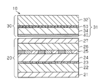
- G06F3/0445—Digitisers, e.g. for touch screens or touch pads, characterised by the transducing means by capacitive means using two or more layers of sensing electrodes, e.g. using two layers of electrodes separated by a dielectric layer
-
- G—PHYSICS
- G06—COMPUTING OR CALCULATING; COUNTING
- G06F—ELECTRIC DIGITAL DATA PROCESSING
- G06F3/00—Input arrangements for transferring data to be processed into a form capable of being handled by the computer; Output arrangements for transferring data from processing unit to output unit, e.g. interface arrangements
- G06F3/01—Input arrangements or combined input and output arrangements for interaction between user and computer
- G06F3/03—Arrangements for converting the position or the displacement of a member into a coded form
- G06F3/041—Digitisers, e.g. for touch screens or touch pads, characterised by the transducing means
- G06F3/047—Digitisers, e.g. for touch screens or touch pads, characterised by the transducing means using sets of wires, e.g. crossed wires
-
- G—PHYSICS
- G09—EDUCATION; CRYPTOGRAPHY; DISPLAY; ADVERTISING; SEALS
- G09G—ARRANGEMENTS OR CIRCUITS FOR CONTROL OF INDICATING DEVICES USING STATIC MEANS TO PRESENT VARIABLE INFORMATION
- G09G5/00—Control arrangements or circuits for visual indicators common to cathode-ray tube indicators and other visual indicators
- G09G5/003—Details of a display terminal, the details relating to the control arrangement of the display terminal and to the interfaces thereto
-
- G—PHYSICS
- G06—COMPUTING OR CALCULATING; COUNTING
- G06F—ELECTRIC DIGITAL DATA PROCESSING
- G06F2203/00—Indexing scheme relating to G06F3/00 - G06F3/048
- G06F2203/041—Indexing scheme relating to G06F3/041 - G06F3/045
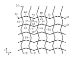
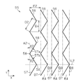
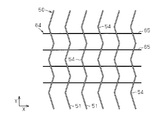
- G06F2203/04112—Electrode mesh in capacitive digitiser: electrode for touch sensing is formed of a mesh of very fine, normally metallic, interconnected lines that are almost invisible to see. This provides a quite large but transparent electrode surface, without need for ITO or similar transparent conductive material
-
- G—PHYSICS
- G09—EDUCATION; CRYPTOGRAPHY; DISPLAY; ADVERTISING; SEALS
- G09G—ARRANGEMENTS OR CIRCUITS FOR CONTROL OF INDICATING DEVICES USING STATIC MEANS TO PRESENT VARIABLE INFORMATION
- G09G2300/00—Aspects of the constitution of display devices
- G09G2300/04—Structural and physical details of display devices
- G09G2300/0421—Structural details of the set of electrodes
- G09G2300/0426—Layout of electrodes and connections
Landscapes
- Engineering & Computer Science (AREA)
- Theoretical Computer Science (AREA)
- General Engineering & Computer Science (AREA)
- Physics & Mathematics (AREA)
- General Physics & Mathematics (AREA)
- Human Computer Interaction (AREA)
- Computer Hardware Design (AREA)
- Position Input By Displaying (AREA)
- Nonlinear Science (AREA)
- Liquid Crystal (AREA)
- Mathematical Physics (AREA)
- Chemical & Material Sciences (AREA)
- Crystallography & Structural Chemistry (AREA)
- Optics & Photonics (AREA)
Applications Claiming Priority (3)
| Application Number | Priority Date | Filing Date | Title |
|---|---|---|---|
| JPJP-P-2013-011262 | 2013-01-24 | ||
| JP2013011262 | 2013-01-24 | ||
| PCT/JP2014/051475 WO2014115831A1 (ja) | 2013-01-24 | 2014-01-24 | タッチパネル、および、表示装置 |
Publications (1)
| Publication Number | Publication Date |
|---|---|
| KR20150108356A true KR20150108356A (ko) | 2015-09-25 |
Family
ID=51227620
Family Applications (1)
| Application Number | Title | Priority Date | Filing Date |
|---|---|---|---|
| KR1020157016562A Ceased KR20150108356A (ko) | 2013-01-24 | 2014-01-24 | 터치 패널 및 표시 장치 |
Country Status (7)
Cited By (1)
| Publication number | Priority date | Publication date | Assignee | Title |
|---|---|---|---|---|
| KR20200066729A (ko) * | 2018-08-06 | 2020-06-10 | 윤구(구안) 테크놀로지 컴퍼니 리미티드 | 디스플레이 패널, 디스플레이 스크린 및 디스플레이 단말기 |
Families Citing this family (22)
| Publication number | Priority date | Publication date | Assignee | Title |
|---|---|---|---|---|
| WO2014115831A1 (ja) * | 2013-01-24 | 2014-07-31 | 凸版印刷株式会社 | タッチパネル、および、表示装置 |
| JP2014191575A (ja) * | 2013-03-27 | 2014-10-06 | Dainippon Printing Co Ltd | タッチパネル用電極基板、及びタッチパネル、ならびに画像表示装置 |
| CN105469732B (zh) * | 2014-09-05 | 2019-02-05 | 联想(北京)有限公司 | 显示装置和电子设备 |
| JP2016126730A (ja) * | 2015-01-08 | 2016-07-11 | 凸版印刷株式会社 | タッチセンサ用電極、タッチパネル、および、表示装置 |
| JP2016126731A (ja) * | 2015-01-08 | 2016-07-11 | 凸版印刷株式会社 | タッチセンサ用電極、タッチパネル、および、表示装置 |
| CN104536634A (zh) * | 2015-01-26 | 2015-04-22 | 京东方科技集团股份有限公司 | 一种触摸屏及显示装置 |
| CN104638016A (zh) | 2015-01-28 | 2015-05-20 | 京东方科技集团股份有限公司 | 薄膜晶体管及制备方法、阵列基板及制备方法、显示装置 |
| JP2016173697A (ja) * | 2015-03-17 | 2016-09-29 | 富士フイルム株式会社 | タッチパネル用透明導電フィルムおよびタッチパネル |
| CN104978070A (zh) * | 2015-07-27 | 2015-10-14 | 苏州触动电子科技有限公司 | 一种消除衍射的触控膜 |
| CN105138186B (zh) * | 2015-10-08 | 2018-01-23 | 京东方科技集团股份有限公司 | 一种触控电极结构、触摸屏及显示装置 |
| CN107562249B (zh) * | 2016-07-01 | 2024-04-30 | 瀚宇彩晶股份有限公司 | 触控显示装置 |
| KR20190039606A (ko) * | 2016-08-30 | 2019-04-12 | 텍추얼 랩스 컴퍼니 | 정전용량식 센서 |
| JP2018049557A (ja) * | 2016-09-23 | 2018-03-29 | 富士通コンポーネント株式会社 | タッチパネル |
| CN109426399B (zh) * | 2017-09-05 | 2022-03-01 | 瀚宇彩晶股份有限公司 | 触控显示装置 |
| JP7039248B2 (ja) | 2017-10-20 | 2022-03-22 | 株式会社Vtsタッチセンサー | 導電性フィルム、タッチパネル、および、表示装置 |
| CN108170307A (zh) * | 2017-11-30 | 2018-06-15 | 云谷(固安)科技有限公司 | 一种触控面板及触控显示装置 |
| US10928951B2 (en) * | 2018-05-31 | 2021-02-23 | Japan Aviation Electronics Industry, Limited | Touch panel having high resistance to static electricity |
| JP7281940B2 (ja) * | 2019-03-28 | 2023-05-26 | 株式会社ジャパンディスプレイ | 検出装置付き表示機器 |
| WO2021005905A1 (ja) * | 2019-07-05 | 2021-01-14 | 株式会社ワコム | 位置検出用センサ及び電子機器 |
| TWI708173B (zh) * | 2019-08-26 | 2020-10-21 | 友達光電股份有限公司 | 觸控面板 |
| JP7469485B2 (ja) * | 2020-08-27 | 2024-04-16 | 富士フイルム株式会社 | タッチパネル用導電部材およびタッチパネル |
| CN114284304B (zh) * | 2021-12-30 | 2025-04-15 | 上海天马微电子有限公司 | 显示模组和显示装置 |
Family Cites Families (26)
| Publication number | Priority date | Publication date | Assignee | Title |
|---|---|---|---|---|
| JPH11110115A (ja) * | 1997-09-30 | 1999-04-23 | Fujitsu General Ltd | デジタイザ装置 |
| JP4992561B2 (ja) * | 2007-06-08 | 2012-08-08 | Tdk株式会社 | インモールド用金型、タッチパネル用中間体製造方法、タッチパネル用中間体およびタッチパネル |
| EP2079008A1 (en) * | 2007-12-26 | 2009-07-15 | TPO Displays Corp. | Position sensing display |
| JP5174575B2 (ja) * | 2008-07-31 | 2013-04-03 | グンゼ株式会社 | タッチパネル |
| US8269744B2 (en) * | 2008-09-05 | 2012-09-18 | Mitsubishi Electric Corporation | Touch screen, touch panel and display device |
| JP4869309B2 (ja) * | 2008-09-05 | 2012-02-08 | 三菱電機株式会社 | タッチスクリーン、タッチパネル及び表示装置 |
| EP3056978A1 (en) * | 2009-02-26 | 2016-08-17 | 3M Innovative Properties Company | Touch screen sensor and patterned substrate having overlaid micropatterns with low visibility |
| DE102009014757A1 (de) * | 2009-03-27 | 2010-10-07 | Polyic Gmbh & Co. Kg | Elektrische Funktionsschicht, Herstellungsverfahren und Verwendung dazu |
| GB0913734D0 (en) * | 2009-08-06 | 2009-09-16 | Binstead Ronald P | Masked touch sensors |
| WO2011017891A1 (zh) * | 2009-08-12 | 2011-02-17 | 智点科技有限公司 | 一种有源触控系统 |
| US8599150B2 (en) * | 2009-10-29 | 2013-12-03 | Atmel Corporation | Touchscreen electrode configuration |
| TWM379805U (en) * | 2009-12-03 | 2010-05-01 | Emerging Display Tech Corp | Capacitance touch panel with eliminating moire fringe |
| JP5645581B2 (ja) | 2010-10-05 | 2014-12-24 | 富士フイルム株式会社 | タッチパネル |
| DE102011014748B4 (de) * | 2011-03-22 | 2022-10-27 | Polyic Gmbh & Co. Kg | Schichtkörper, Herstellungsverfahren und Verwendung dazu |
| JP2012221120A (ja) * | 2011-04-06 | 2012-11-12 | Fujitsu Component Ltd | タッチパネル |
| US8797285B2 (en) * | 2011-04-18 | 2014-08-05 | Atmel Corporation | Panel |
| WO2013039050A1 (ja) * | 2011-09-13 | 2013-03-21 | グンゼ株式会社 | タッチパネル |
| US8963561B2 (en) * | 2011-11-03 | 2015-02-24 | Atmel Corporation | Randomizing one or more micro-features of a touch sensor |
| US9116582B2 (en) * | 2012-02-09 | 2015-08-25 | Qualcomm Technologies, Inc. | Capacitive touch panel having protrusions formed between drive and/or sensor electrodes |
| WO2014115831A1 (ja) * | 2013-01-24 | 2014-07-31 | 凸版印刷株式会社 | タッチパネル、および、表示装置 |
| US9715314B2 (en) * | 2013-06-24 | 2017-07-25 | Microsoft Technology Licensing, Llc | Capacitive touch sensor having pseudo jumpers |
| JP2016126731A (ja) * | 2015-01-08 | 2016-07-11 | 凸版印刷株式会社 | タッチセンサ用電極、タッチパネル、および、表示装置 |
| JP2016126730A (ja) * | 2015-01-08 | 2016-07-11 | 凸版印刷株式会社 | タッチセンサ用電極、タッチパネル、および、表示装置 |
| KR20160088530A (ko) * | 2015-01-15 | 2016-07-26 | 삼성디스플레이 주식회사 | 터치 패널 |
| JP2016212517A (ja) * | 2015-04-30 | 2016-12-15 | 凸版印刷株式会社 | 導電性フィルム、タッチパネル、および、表示装置 |
| JP6636717B2 (ja) * | 2015-04-30 | 2020-01-29 | 株式会社Vtsタッチセンサー | 導電性フィルム、タッチパネル、および、表示装置 |
-
2014
- 2014-01-24 WO PCT/JP2014/051475 patent/WO2014115831A1/ja active Application Filing
- 2014-01-24 KR KR1020157016562A patent/KR20150108356A/ko not_active Ceased
- 2014-01-24 TW TW103102578A patent/TWI550450B/zh active
- 2014-01-24 JP JP2014558627A patent/JP5930076B2/ja not_active Expired - Fee Related
- 2014-01-24 CN CN201480003035.9A patent/CN104798020A/zh active Pending
- 2014-01-24 EP EP14742944.3A patent/EP2950186A4/en not_active Withdrawn
-
2015
- 2015-07-24 US US14/808,096 patent/US20150331526A1/en not_active Abandoned
-
2016
- 2016-05-02 JP JP2016092812A patent/JP6296093B2/ja active Active
Cited By (1)
| Publication number | Priority date | Publication date | Assignee | Title |
|---|---|---|---|---|
| KR20200066729A (ko) * | 2018-08-06 | 2020-06-10 | 윤구(구안) 테크놀로지 컴퍼니 리미티드 | 디스플레이 패널, 디스플레이 스크린 및 디스플레이 단말기 |
Also Published As
| Publication number | Publication date |
|---|---|
| JP5930076B2 (ja) | 2016-06-08 |
| JP6296093B2 (ja) | 2018-03-20 |
| JPWO2014115831A1 (ja) | 2017-01-26 |
| EP2950186A1 (en) | 2015-12-02 |
| TWI550450B (zh) | 2016-09-21 |
| US20150331526A1 (en) | 2015-11-19 |
| CN104798020A (zh) | 2015-07-22 |
| JP2016136444A (ja) | 2016-07-28 |
| WO2014115831A1 (ja) | 2014-07-31 |
| TW201439853A (zh) | 2014-10-16 |
| EP2950186A4 (en) | 2016-09-28 |
Similar Documents
| Publication | Publication Date | Title |
|---|---|---|
| KR20150108356A (ko) | 터치 패널 및 표시 장치 | |
| CN104885042B (zh) | 触摸面板及显示装置 | |
| US9740322B2 (en) | Touch panel and liquid crystal display device having the touch panel | |
| CN107037625B (zh) | 具有传感器的显示装置以及传感器装置 | |
| KR101719058B1 (ko) | 센서를 갖는 표시 장치 | |
| US11822749B2 (en) | Touch panel and touch device | |
| US20180052359A1 (en) | Color filter substrate, sensor substrate and display device | |
| WO2016136661A1 (ja) | タッチセンサ付き表示装置 | |
| US10416805B2 (en) | Touch display apparatus | |
| WO2014021226A1 (ja) | タッチパネル基板及び表示装置 | |
| JP6504990B2 (ja) | 液晶表示装置 | |
| US10416798B2 (en) | Touch display apparatus | |
| KR20170080892A (ko) | 터치패널 및 이를 포함하는 표시장치 | |
| JP6409117B2 (ja) | タッチセンサ付き表示装置 | |
| JP2016126730A (ja) | タッチセンサ用電極、タッチパネル、および、表示装置 | |
| JP2016212518A (ja) | 導電性フィルム、タッチパネル、および、表示装置 | |
| JP2016126731A (ja) | タッチセンサ用電極、タッチパネル、および、表示装置 | |
| US20210405811A1 (en) | Touch control structure, method of detecting touch using touch control structure, touch control apparatus, and touch control display apparatus | |
| JP2018081486A (ja) | 導電性フィルム、タッチパネル、および、表示装置 |
Legal Events
| Date | Code | Title | Description |
|---|---|---|---|
| PA0105 | International application |
Patent event date: 20150622 Patent event code: PA01051R01D Comment text: International Patent Application |
|
| PG1501 | Laying open of application | ||
| PN2301 | Change of applicant |
Patent event date: 20180622 Comment text: Notification of Change of Applicant Patent event code: PN23011R01D |
|
| PA0201 | Request for examination |
Patent event code: PA02012R01D Patent event date: 20190118 Comment text: Request for Examination of Application |
|
| E902 | Notification of reason for refusal | ||
| PE0902 | Notice of grounds for rejection |
Comment text: Notification of reason for refusal Patent event date: 20200623 Patent event code: PE09021S01D |
|
| E601 | Decision to refuse application | ||
| PE0601 | Decision on rejection of patent |
Patent event date: 20200918 Comment text: Decision to Refuse Application Patent event code: PE06012S01D Patent event date: 20200623 Comment text: Notification of reason for refusal Patent event code: PE06011S01I |