KR20150106372A - Display device and method of drving the same - Google Patents
Display device and method of drving the same Download PDFInfo
- Publication number
- KR20150106372A KR20150106372A KR1020150033453A KR20150033453A KR20150106372A KR 20150106372 A KR20150106372 A KR 20150106372A KR 1020150033453 A KR1020150033453 A KR 1020150033453A KR 20150033453 A KR20150033453 A KR 20150033453A KR 20150106372 A KR20150106372 A KR 20150106372A
- Authority
- KR
- South Korea
- Prior art keywords
- transistor
- gate
- signal
- stage
- output
- Prior art date
Links
Images


Classifications
-
- G—PHYSICS
- G09—EDUCATION; CRYPTOGRAPHY; DISPLAY; ADVERTISING; SEALS
- G09G—ARRANGEMENTS OR CIRCUITS FOR CONTROL OF INDICATING DEVICES USING STATIC MEANS TO PRESENT VARIABLE INFORMATION
- G09G3/00—Control arrangements or circuits, of interest only in connection with visual indicators other than cathode-ray tubes
- G09G3/20—Control arrangements or circuits, of interest only in connection with visual indicators other than cathode-ray tubes for presentation of an assembly of a number of characters, e.g. a page, by composing the assembly by combination of individual elements arranged in a matrix no fixed position being assigned to or needed to be assigned to the individual characters or partial characters
- G09G3/34—Control arrangements or circuits, of interest only in connection with visual indicators other than cathode-ray tubes for presentation of an assembly of a number of characters, e.g. a page, by composing the assembly by combination of individual elements arranged in a matrix no fixed position being assigned to or needed to be assigned to the individual characters or partial characters by control of light from an independent source
- G09G3/36—Control arrangements or circuits, of interest only in connection with visual indicators other than cathode-ray tubes for presentation of an assembly of a number of characters, e.g. a page, by composing the assembly by combination of individual elements arranged in a matrix no fixed position being assigned to or needed to be assigned to the individual characters or partial characters by control of light from an independent source using liquid crystals
- G09G3/3611—Control of matrices with row and column drivers
- G09G3/3674—Details of drivers for scan electrodes
- G09G3/3677—Details of drivers for scan electrodes suitable for active matrices only
-
- G—PHYSICS
- G09—EDUCATION; CRYPTOGRAPHY; DISPLAY; ADVERTISING; SEALS
- G09G—ARRANGEMENTS OR CIRCUITS FOR CONTROL OF INDICATING DEVICES USING STATIC MEANS TO PRESENT VARIABLE INFORMATION
- G09G3/00—Control arrangements or circuits, of interest only in connection with visual indicators other than cathode-ray tubes
- G09G3/20—Control arrangements or circuits, of interest only in connection with visual indicators other than cathode-ray tubes for presentation of an assembly of a number of characters, e.g. a page, by composing the assembly by combination of individual elements arranged in a matrix no fixed position being assigned to or needed to be assigned to the individual characters or partial characters
-
- G—PHYSICS
- G06—COMPUTING; CALCULATING OR COUNTING
- G06F—ELECTRIC DIGITAL DATA PROCESSING
- G06F3/00—Input arrangements for transferring data to be processed into a form capable of being handled by the computer; Output arrangements for transferring data from processing unit to output unit, e.g. interface arrangements
- G06F3/01—Input arrangements or combined input and output arrangements for interaction between user and computer
- G06F3/03—Arrangements for converting the position or the displacement of a member into a coded form
- G06F3/041—Digitisers, e.g. for touch screens or touch pads, characterised by the transducing means
- G06F3/0416—Control or interface arrangements specially adapted for digitisers
- G06F3/04166—Details of scanning methods, e.g. sampling time, grouping of sub areas or time sharing with display driving
-
- G—PHYSICS
- G09—EDUCATION; CRYPTOGRAPHY; DISPLAY; ADVERTISING; SEALS
- G09G—ARRANGEMENTS OR CIRCUITS FOR CONTROL OF INDICATING DEVICES USING STATIC MEANS TO PRESENT VARIABLE INFORMATION
- G09G3/00—Control arrangements or circuits, of interest only in connection with visual indicators other than cathode-ray tubes
- G09G3/20—Control arrangements or circuits, of interest only in connection with visual indicators other than cathode-ray tubes for presentation of an assembly of a number of characters, e.g. a page, by composing the assembly by combination of individual elements arranged in a matrix no fixed position being assigned to or needed to be assigned to the individual characters or partial characters
- G09G3/22—Control arrangements or circuits, of interest only in connection with visual indicators other than cathode-ray tubes for presentation of an assembly of a number of characters, e.g. a page, by composing the assembly by combination of individual elements arranged in a matrix no fixed position being assigned to or needed to be assigned to the individual characters or partial characters using controlled light sources
- G09G3/30—Control arrangements or circuits, of interest only in connection with visual indicators other than cathode-ray tubes for presentation of an assembly of a number of characters, e.g. a page, by composing the assembly by combination of individual elements arranged in a matrix no fixed position being assigned to or needed to be assigned to the individual characters or partial characters using controlled light sources using electroluminescent panels
- G09G3/32—Control arrangements or circuits, of interest only in connection with visual indicators other than cathode-ray tubes for presentation of an assembly of a number of characters, e.g. a page, by composing the assembly by combination of individual elements arranged in a matrix no fixed position being assigned to or needed to be assigned to the individual characters or partial characters using controlled light sources using electroluminescent panels semiconductive, e.g. using light-emitting diodes [LED]
- G09G3/3208—Control arrangements or circuits, of interest only in connection with visual indicators other than cathode-ray tubes for presentation of an assembly of a number of characters, e.g. a page, by composing the assembly by combination of individual elements arranged in a matrix no fixed position being assigned to or needed to be assigned to the individual characters or partial characters using controlled light sources using electroluminescent panels semiconductive, e.g. using light-emitting diodes [LED] organic, e.g. using organic light-emitting diodes [OLED]
- G09G3/3266—Details of drivers for scan electrodes
-
- G—PHYSICS
- G09—EDUCATION; CRYPTOGRAPHY; DISPLAY; ADVERTISING; SEALS
- G09G—ARRANGEMENTS OR CIRCUITS FOR CONTROL OF INDICATING DEVICES USING STATIC MEANS TO PRESENT VARIABLE INFORMATION
- G09G3/00—Control arrangements or circuits, of interest only in connection with visual indicators other than cathode-ray tubes
- G09G3/20—Control arrangements or circuits, of interest only in connection with visual indicators other than cathode-ray tubes for presentation of an assembly of a number of characters, e.g. a page, by composing the assembly by combination of individual elements arranged in a matrix no fixed position being assigned to or needed to be assigned to the individual characters or partial characters
- G09G3/34—Control arrangements or circuits, of interest only in connection with visual indicators other than cathode-ray tubes for presentation of an assembly of a number of characters, e.g. a page, by composing the assembly by combination of individual elements arranged in a matrix no fixed position being assigned to or needed to be assigned to the individual characters or partial characters by control of light from an independent source
- G09G3/36—Control arrangements or circuits, of interest only in connection with visual indicators other than cathode-ray tubes for presentation of an assembly of a number of characters, e.g. a page, by composing the assembly by combination of individual elements arranged in a matrix no fixed position being assigned to or needed to be assigned to the individual characters or partial characters by control of light from an independent source using liquid crystals
- G09G3/3611—Control of matrices with row and column drivers
- G09G3/3685—Details of drivers for data electrodes
- G09G3/3688—Details of drivers for data electrodes suitable for active matrices only
-
- G—PHYSICS
- G09—EDUCATION; CRYPTOGRAPHY; DISPLAY; ADVERTISING; SEALS
- G09G—ARRANGEMENTS OR CIRCUITS FOR CONTROL OF INDICATING DEVICES USING STATIC MEANS TO PRESENT VARIABLE INFORMATION
- G09G3/00—Control arrangements or circuits, of interest only in connection with visual indicators other than cathode-ray tubes
- G09G3/20—Control arrangements or circuits, of interest only in connection with visual indicators other than cathode-ray tubes for presentation of an assembly of a number of characters, e.g. a page, by composing the assembly by combination of individual elements arranged in a matrix no fixed position being assigned to or needed to be assigned to the individual characters or partial characters
- G09G3/34—Control arrangements or circuits, of interest only in connection with visual indicators other than cathode-ray tubes for presentation of an assembly of a number of characters, e.g. a page, by composing the assembly by combination of individual elements arranged in a matrix no fixed position being assigned to or needed to be assigned to the individual characters or partial characters by control of light from an independent source
- G09G3/36—Control arrangements or circuits, of interest only in connection with visual indicators other than cathode-ray tubes for presentation of an assembly of a number of characters, e.g. a page, by composing the assembly by combination of individual elements arranged in a matrix no fixed position being assigned to or needed to be assigned to the individual characters or partial characters by control of light from an independent source using liquid crystals
- G09G3/3611—Control of matrices with row and column drivers
- G09G3/3696—Generation of voltages supplied to electrode drivers
-
- G—PHYSICS
- G11—INFORMATION STORAGE
- G11C—STATIC STORES
- G11C19/00—Digital stores in which the information is moved stepwise, e.g. shift registers
- G11C19/28—Digital stores in which the information is moved stepwise, e.g. shift registers using semiconductor elements
-
- G—PHYSICS
- G09—EDUCATION; CRYPTOGRAPHY; DISPLAY; ADVERTISING; SEALS
- G09G—ARRANGEMENTS OR CIRCUITS FOR CONTROL OF INDICATING DEVICES USING STATIC MEANS TO PRESENT VARIABLE INFORMATION
- G09G2300/00—Aspects of the constitution of display devices
- G09G2300/08—Active matrix structure, i.e. with use of active elements, inclusive of non-linear two terminal elements, in the pixels together with light emitting or modulating elements
- G09G2300/0809—Several active elements per pixel in active matrix panels
-
- G—PHYSICS
- G09—EDUCATION; CRYPTOGRAPHY; DISPLAY; ADVERTISING; SEALS
- G09G—ARRANGEMENTS OR CIRCUITS FOR CONTROL OF INDICATING DEVICES USING STATIC MEANS TO PRESENT VARIABLE INFORMATION
- G09G2310/00—Command of the display device
- G09G2310/02—Addressing, scanning or driving the display screen or processing steps related thereto
- G09G2310/0202—Addressing of scan or signal lines
- G09G2310/0213—Addressing of scan or signal lines controlling the sequence of the scanning lines with respect to the patterns to be displayed, e.g. to save power
-
- G—PHYSICS
- G09—EDUCATION; CRYPTOGRAPHY; DISPLAY; ADVERTISING; SEALS
- G09G—ARRANGEMENTS OR CIRCUITS FOR CONTROL OF INDICATING DEVICES USING STATIC MEANS TO PRESENT VARIABLE INFORMATION
- G09G2310/00—Command of the display device
- G09G2310/02—Addressing, scanning or driving the display screen or processing steps related thereto
- G09G2310/0243—Details of the generation of driving signals
- G09G2310/0248—Precharge or discharge of column electrodes before or after applying exact column voltages
-
- G—PHYSICS
- G09—EDUCATION; CRYPTOGRAPHY; DISPLAY; ADVERTISING; SEALS
- G09G—ARRANGEMENTS OR CIRCUITS FOR CONTROL OF INDICATING DEVICES USING STATIC MEANS TO PRESENT VARIABLE INFORMATION
- G09G2310/00—Command of the display device
- G09G2310/02—Addressing, scanning or driving the display screen or processing steps related thereto
- G09G2310/0264—Details of driving circuits
- G09G2310/0267—Details of drivers for scan electrodes, other than drivers for liquid crystal, plasma or OLED displays
-
- G—PHYSICS
- G09—EDUCATION; CRYPTOGRAPHY; DISPLAY; ADVERTISING; SEALS
- G09G—ARRANGEMENTS OR CIRCUITS FOR CONTROL OF INDICATING DEVICES USING STATIC MEANS TO PRESENT VARIABLE INFORMATION
- G09G2310/00—Command of the display device
- G09G2310/02—Addressing, scanning or driving the display screen or processing steps related thereto
- G09G2310/0264—Details of driving circuits
- G09G2310/0286—Details of a shift registers arranged for use in a driving circuit
-
- G—PHYSICS
- G09—EDUCATION; CRYPTOGRAPHY; DISPLAY; ADVERTISING; SEALS
- G09G—ARRANGEMENTS OR CIRCUITS FOR CONTROL OF INDICATING DEVICES USING STATIC MEANS TO PRESENT VARIABLE INFORMATION
- G09G2310/00—Command of the display device
- G09G2310/04—Partial updating of the display screen
-
- G—PHYSICS
- G09—EDUCATION; CRYPTOGRAPHY; DISPLAY; ADVERTISING; SEALS
- G09G—ARRANGEMENTS OR CIRCUITS FOR CONTROL OF INDICATING DEVICES USING STATIC MEANS TO PRESENT VARIABLE INFORMATION
- G09G2330/00—Aspects of power supply; Aspects of display protection and defect management
- G09G2330/02—Details of power systems and of start or stop of display operation
- G09G2330/021—Power management, e.g. power saving
-
- G—PHYSICS
- G09—EDUCATION; CRYPTOGRAPHY; DISPLAY; ADVERTISING; SEALS
- G09G—ARRANGEMENTS OR CIRCUITS FOR CONTROL OF INDICATING DEVICES USING STATIC MEANS TO PRESENT VARIABLE INFORMATION
- G09G2340/00—Aspects of display data processing
- G09G2340/04—Changes in size, position or resolution of an image
- G09G2340/0442—Handling or displaying different aspect ratios, or changing the aspect ratio
-
- G—PHYSICS
- G09—EDUCATION; CRYPTOGRAPHY; DISPLAY; ADVERTISING; SEALS
- G09G—ARRANGEMENTS OR CIRCUITS FOR CONTROL OF INDICATING DEVICES USING STATIC MEANS TO PRESENT VARIABLE INFORMATION
- G09G2340/00—Aspects of display data processing
- G09G2340/04—Changes in size, position or resolution of an image
- G09G2340/0464—Positioning
- G09G2340/0471—Vertical positioning
-
- G—PHYSICS
- G09—EDUCATION; CRYPTOGRAPHY; DISPLAY; ADVERTISING; SEALS
- G09G—ARRANGEMENTS OR CIRCUITS FOR CONTROL OF INDICATING DEVICES USING STATIC MEANS TO PRESENT VARIABLE INFORMATION
- G09G2354/00—Aspects of interface with display user
Abstract
Description
본 발명은 표시장치에 관한 것으로서, 특히, 소비전력을 감소시킬 수 있는 표시장치 및 그 구동방법에 관한 것이다. BACKGROUND OF THE
휴대전화, 테블릿PC, 노트북 등을 포함한 다양한 종류의 전자제품에는 평판표시장치(FPD: Flat Panel Display)가 이용되고 있다. 평판표시장치에는, 액정표시장치(LCD: Liquid Crystal Display), 플라즈마 디스플레이 장치(PDP: Plasma Display), 유기발광표시장치(OLED: Organic Light Emitting Display), 전기영동표시장치(EPD: Electrophoretic Display) 등이 있다. Flat panel displays (FPDs) are used in various types of electronic products including mobile phones, tablet PCs, and notebook computers. Examples of the flat panel display include a liquid crystal display (LCD), a plasma display (PDP), an organic light emitting display (OLED), an electrophoretic display (EPD) .
평판표시장치(간단히 '표시장치'라 함)들 중에서, 액정표시장치(LCD)는 액정의 광학적 이방성을 이용하여 화상을 표시하는 장치로서, 박형, 소형, 저소비전력 및 고화질 등의 장점이 있기 때문에, 널리 이용되고 있다. 자발광 소자를 이용하며, 별도의 백라이트가 필요 없는 유기발광표시장치(Organic Light Emitting Display) 또한 빠른 응답속도, 높은 발광효율, 높은 휘도 및 큰 시야각과 같은 장점을 가지고 있기 때문에, 차세대 평판표시장치로 주목 받고 있다.Among the flat panel display devices (simply referred to as 'display devices'), a liquid crystal display device (LCD) is an apparatus for displaying an image using optical anisotropy of liquid crystal, and has advantages of thinness, small size, low power consumption, , Are widely used. Organic Light Emitting Display (OLED), which uses a self-luminous element and does not require a separate backlight, has advantages such as fast response speed, high luminous efficiency, high luminance and a large viewing angle. It is attracting attention.
일반적으로 표시장치는 영상을 표시하는 패널, 상기 패널에 형성되어 있는 게이트 라인들에 순차적으로 스캔신호를 공급하기 위한 게이트 드라이버, 상기 패널에 형성되어 있는 데이터 라인들에 데이터 전압을 공급하기 위한 데이터 드라이버 및 상기 게이트 드라이버와 상기 데이터 드라이버를 제어하기 위한 타이밍 컨트롤러를 포함하고 있다. In general, a display device includes a panel for displaying an image, a gate driver for sequentially supplying a scan signal to gate lines formed on the panel, a data driver for supplying a data voltage to data lines formed on the panel, And a timing controller for controlling the gate driver and the data driver.
게이트 드라이버가 각 픽셀의 스위칭 소자들을 액티브 매트릭스 방식으로 구동함으로써, 동적인 영상이 표시된다. 게이트 드라이버는 집적회로(Integrated Circuit, IC) 형태로 구성되어, 패널 또는 필름에 장착되거나, Gate-In-Panel 방식을 이용하여 패널에 직접 형성될 수 있다. 게이트 드라이버는 표시장치의 픽셀이 형성된 패널과 별도로 구비되어, 상기 패널과 전기적으로 연결될 수 있다. 예를 들어, 게이트 드라이버는, 별도의 기판에, Chip-On-Film(COF) 방식, Chip-On-Glass(COG) 방식 또는 그 밖의 여러 가지 방식을 이용하여, 상기 패널과 전기적으로 연결될 수 있다. The gate driver drives the switching elements of each pixel in an active matrix manner, so that a dynamic image is displayed. The gate driver may be formed in the form of an integrated circuit (IC), and may be mounted on a panel or a film, or may be formed directly on the panel using a gate-in-panel method. The gate driver may be provided separately from the panel on which the pixels of the display device are formed, and may be electrically connected to the panel. For example, the gate driver may be electrically connected to the panel using a chip-on-film (COF) method, a chip-on-glass (COG) .
게이트 드라이버는 소정의 클록에 동기하여 패널에 형성된 게이트 라인에 스캔신호를 출력하는 복수의 스테이지들로 이루어진, 쉬프트 레지스터(shift register)를 포함한다. 원활한 영상출력 또는 그 외의 여러 가지 구동 조건들을 만족하기 위해서, 게이트 드라이버는, 일정한 주파수에 맞춰 구동되어, 게이트 라인들에 순차적으로 스캔신호를 출력하는 동작을, 매 프레임마다 반복적으로 수행한다. The gate driver includes a shift register composed of a plurality of stages for outputting a scan signal to a gate line formed on the panel in synchronization with a predetermined clock. In order to satisfy a smooth video output or various other driving conditions, the gate driver is driven in accordance with a constant frequency, and performs an operation of sequentially outputting a scan signal to the gate lines repeatedly every frame.
다양한 종류의 영상을 출력하는 표시장치에서, 일시적인 구동조건을 충족하기 위해, 항상 빠른 주파수로 게이트 드라이버를 구동하거나, 모든 스테이지들로부터 순차적으로 스캔신호가 출력되도록 게이트 드라이버를 구동하는 것은, 소비전력을 낭비시킬 수 있다. In a display device for outputting various kinds of images, driving a gate driver always at a fast frequency in order to satisfy a temporary driving condition, or driving a gate driver such that a scan signal is sequentially output from all stages, It can be wasted.
또한, 항상 동일한 주파수로 모든 스테이지들로부터 순차적으로 스캔신호가 출력됨에 따라, 표시장치에서, 터치인식 또는 지문인식과 같은 추가기능들의 수행이 제한될 수 있다. 터치인식 또는 지문인식과 같은 추가기능들은, 게이트 드라이버가 스캔신호를 출력하지 않을 때 수행되는 것이 유리할 수 있다. 따라서, 추가기능을 위한 작업들은 두 프레임(Frame) 사이의 휴지기간(Blank Time)에 수행된다. 이런 추가기능들을 수행하기 위한 시간을 더 확보하기 위해서는, 각 프레임기간 중 영상을 출력하는 기간이 단축되어야 한다. 그러나, 이것은 픽셀 충전 타임(Pixel charging time)을 감소시킬 수 있으며, 추가기능을 수행함에 따라 발생되는 노이즈 및 픽셀 커플링에 의해, 플리커(Flicker)와 같은 화질 불량이 발생될 수 있다. Further, as the scan signals are sequentially output from all the stages at the same frequency at all times, the performance of additional functions such as touch recognition or fingerprint recognition may be restricted in the display device. Additional functions such as touch recognition or fingerprint recognition may be advantageously performed when the gate driver does not output a scan signal. Thus, tasks for additional functions are performed at a blank time between two frames. In order to secure more time for performing these additional functions, the period of outputting an image during each frame period must be shortened. However, this may reduce the pixel charging time, and image quality defects such as flicker may occur due to noise and pixel coupling caused by performing additional functions.
상술한 기술적 과제를 달성하기 위한 본 발명에 따른 표시장치는, 게이트라인들과 데이터라인들이 형성되어 있는 패널; 상기 패널에 형성되어 있는 데이터라인들로 데이터전압을 공급하는 데이터드라이버; 및 스타트신호에 따라 순차적으로 구동되는 스테이지들로 구성된 게이트 드라이버를 포함하며, 상기 게이트 드라이버는 인에이블신호에 따라 상기스테이지들 중 적어도 하나의 스테이지로부터 출력되는 스캔신호의 출력을 제어한다.According to an aspect of the present invention, there is provided a display device including: a panel having gate lines and data lines formed therein; A data driver for supplying a data voltage to the data lines formed on the panel; And a gate driver configured by stages sequentially driven in accordance with a start signal, the gate driver controlling the output of a scan signal output from at least one of the stages in accordance with an enable signal.
상술한 기술적 과제를 달성하기 위한 본 발명에 따른 표시장치 구동방법은, 일 프레임기간 중, 게이트 드라이버에 인가되는 인에이블 신호에 따라 상기 게이트 드라이버에 포함된 스테이지들 중 적어도 하나의 스테이지와 연결된 게이트 라인으로 스캔신호를 출력하는 단계; 및 상기 일 프레임 기간 중, 상기 인에이블신호에 따라 상기 스테이지들 중 적어도 하나의 스테이지와 연결된 게이트 라인으로 스캔신호를 출력하지 않는 단계를 포함한다.According to another aspect of the present invention, there is provided a method of driving a display device including a gate driver coupled to at least one stage of stages included in the gate driver according to an enable signal applied to the gate driver, Outputting a scan signal to the scan electrode; And not outputting a scan signal to the gate line connected to at least one of the stages in accordance with the enable signal during the one frame period.
본 발명은 일 프레임기간 중에 일부 게이트 라인들로 스캔신호가 인가되는 것을 차단하여, 일부 구동영역의 픽셀들에 데이터가 충전되는 주기를 가변하는 방법을 이용하여 패널을 구동할 수 있다. 예를 들어, 본 발명은, 일 프레임기간에 대응하는 영상이 출력되는 중에, 일부 스테이지들은 스캔신호를 출력하도록 하고, 다른 일부 스테이지들은 스캔신호를 출력하지 않도록 함으로써, 픽셀들을 불필요하게 짧은 주기로 재충전함에 따라 발생되는 소비전력 낭비를 감소시킬 수 있다. 또한, 일 프레임기간에 대응하는 영상이 출력되는 중에, 본 발명은 일부 게이트 라인들로 스캔신호가 출력되는 것을 차단하고, 스캔신호의 출력이 없는 기간에 수행하기 유리한 작업들을 수행할 수 있다.The present invention can drive the panel by blocking the application of the scan signal to some of the gate lines during one frame period and varying the period of time during which the data is charged in the pixels of a certain driving region. For example, according to the present invention, while an image corresponding to one frame period is output, some stages output a scan signal, and some other stages do not output a scan signal, so that pixels are recharged in an unnecessarily short period Thereby reducing the waste of power consumption. In addition, while the image corresponding to one frame period is being output, the present invention can block the output of the scan signal to some gate lines and perform operations that are advantageous in the absence of the scan signal output.
이 뿐만 아니라, 일부 스테이지들의 스캔신호의 출력 주기를 다른 스테이지들의 스캔신호의 출력주기와 다르게 가변시킴으로써, 특정 구동조건에 한정되지 않고, 다양한 구동 환경에 대응이 가능한 표시장치가 구현될 수 있다. In addition, by varying the output period of the scan signal of some of the stages differently from the output period of the scan signals of the other stages, a display device capable of coping with various drive environments can be implemented without being limited to specific drive conditions.
도 1은 본 발명에 따른 표시장치의 구성을 나타낸 예시도.
도 2a는 터치감지기능이 구비된 표시장치의 일예를 도시한 평면도.
도 2b는 터치인식기능이 구비된 표시장치의 또 다른 예를 도시한 평면도.
도 3a내지 도 3c는 본 발명에 따른 표시장치의 구동방법을 설명하기 위한 다양한 예시도들.
도 4는 본 발명의 제1실시예에 따른 표시장치에 적용되는 게이트 드라이버의 구성을 나타낸 예시도.
도 5는 본 발명에 따른 표시장치에 적용되는 신호들의 파형을 나타낸 예시도.
도 6a는 SLC를 기반으로 하는 스테이지를 나타낸 예시도.
도 6b는 HDAC를 기반으로 하는 스테이지를 나타낸 예시도.
도 7은 본 발명에 따른 표시장치에서 구동방법을 설명하기 위한 예시도.
도 8은 본 발명에 따른 표시장치에 적용되는 노드 제어부의 구성을 나타낸 예시도.
도 9는 본 발명에 따른 표시장치를 안정적으로 구동시키기 위한 구동방법을 설명하기 위한 예시도.
도 10은 본 발명에 따른 표시장치를 안정적으로 구동시키기 위한 안정화 회로의 구성을 나타낸 예시도.
도 11은 본 발명의 표시장치에 적용되는 또 다른 구조의 게이트 드라이버를 나타낸 예시도.
도 12는 본 발명의 표시장치에 적용되는 또 다른 구조의 게이트 드라이버를 나타낸 예시도.
도 13은 본 발명의 표시장치에 적용되는 또 다른 구조의 게이트 드라이버를 나타낸 예시도.
도 14는 본 발명의 표시장치에 적용되는 또 다른 구조의 게이트 드라이버를 나타낸 예시도.
도 15 내지 도 18은 도 14의 도시된 게이트 드라이버를 구성하는 스테이지의 다양한 구성도들. 1 is an exemplary view showing a configuration of a display device according to the present invention.
2A is a plan view showing an example of a display device having a touch sensing function.
2B is a plan view showing another example of a display device provided with a touch recognition function.
3A to 3C are various exemplary diagrams for explaining a driving method of a display device according to the present invention.
4 is an exemplary view showing a configuration of a gate driver applied to a display device according to a first embodiment of the present invention;
5 is an exemplary view showing waveforms of signals applied to a display device according to the present invention;
6A is an exemplary diagram illustrating a stage based on SLC;
6B is an exemplary diagram illustrating a stage based on HDAC;
7 is an exemplary view for explaining a driving method in a display device according to the present invention;
FIG. 8 is an exemplary view showing a configuration of a node control unit applied to a display device according to the present invention; FIG.
FIG. 9 is an exemplary view for explaining a driving method for stably driving the display device according to the present invention; FIG.
10 is an exemplary view showing a configuration of a stabilization circuit for stably driving a display device according to the present invention.
11 is an exemplary view showing a gate driver of another structure applied to the display device of the present invention.
12 is an exemplary view showing a gate driver of another structure applied to the display device of the present invention.
13 is an exemplary view showing a gate driver of another structure applied to the display device of the present invention.
14 is an exemplary view showing a gate driver of another structure applied to the display device of the present invention.
Figs. 15 to 18 are various configuration diagrams of stages constituting the gate driver shown in Fig. 14. Fig.
이하, 첨부된 도면을 참조하여 본 발명의 실시예에 대해 상세히 설명한다.Hereinafter, embodiments of the present invention will be described in detail with reference to the accompanying drawings.
본 명세서에서 실시예들은 액정표시장치를 기초로 설명하였으나, 본 발명은 액정표시장치에 한정되지 않고 유기발광표시장치 등 게이트 드라이버가 구비된 모든 표시장치에 적용이 가능하다. Although embodiments have been described herein with reference to a liquid crystal display device, the present invention is not limited to a liquid crystal display device, and can be applied to all display devices including a gate driver such as an organic light emitting display device.
도 1은 본 발명에 따른 표시장치의 구성을 나타낸 예시도이다.1 is an exemplary view showing a configuration of a display device according to the present invention.
도 1를 참조하면, 표시장치(100)는 복수의 화소(P)가 형성되어 화상을 표시하는 표시영역(A/A) 및 표시영역(A/A)의 외곽에 비표시영역(N/A)을 가진 패널(110)을 포함한다. 또한, 표시장치(100)는 게이트 라인들(GL1 to GLg)을 통해 화소(P)에 스캔신호를 출력하는 게이트 드라이버(120)와 데이터 라인들(DL1 to DLd)로 화소(P)에 데이터 전압을 공급하는 데이터 드라이버(130)를 포함한다. 게이트 드라이버(120)와 데이터 드라이버(130)는 패널(110)상에 구비될 수 있다. 상기 게이트 드라이버(120)와 데이터 드라이버(130)를 제어하는 시그널은 타이밍 컨트롤러(140)로부터 제공될 수 있다.1, the
패널(110)은 영상을 출력하는 기능을 수행한다. 패널(110)의 구성은 상기 표시장치의 종류에 따라 달라질 수 있다. 본 발명에 따른 표시장치가 액정표시장치(LCD)인 경우, 패널(110)은 두 장의 기판 사이에 액정층이 형성되어 있는 액정패널이 될 수 있다. 이 경우, 액정패널을 구성하는 기판 중 하나의 기판에는, 다수의 데이터 라인들(DL1 to DLd), 다수의 게이트 라인들(GL1 to GLg), 데이터 라인들과 게이트 라인들과 전기적으로 연결되어 픽셀들을 구동하는 다수의 박막트랜지스터(Thin Film Transistor: TFT)들이 구비된다. 패널(110)에는 데이터 전압을 충전시키기 위한 다수의 픽셀전극들 및 픽셀전극과 함께 액정층에 구비된 액정을 구동하기 위한 공통전극이 구비된다. The
상술하였듯이 패널(110)은 유기발광패널로 구성될 수도 있다. 이 경우, 패널(110)에 구비된 각각의 픽셀은, 유기발광다이오드(Organic Light-Emitting Diode: OLED), 상기 데이터 라인(DL)들과 상기 게이트 라인(GL)들에 접속되어 상기 유기발광다이오드를 제어하기 위한 복수의 박막트랜지스터들 및 스토리지 커패시터를 포함될 수 있다. As described above, the
게이트 드라이버(120)는 타이밍 컨트롤러(140)로부터 전송되는 게이트 제어신호(GCS)를 이용하여 스캔신호를 게이트 라인들에 출력한다. 본 명세서에서, 스캔신호는, 게이트 라인을 통해 전송되어 픽셀들의 스위칭 트랜지스터를 턴온 시켜, 픽셀들을 데이터 라인에서부터 인가되는 데이터 전압으로 충전시키는 신호를 지칭한다. 또한, 스위칭 트랜지스터를 턴오프시키는 신호는 게이트 오프 신호라 한다. 스위칭 트랜지스터가 N타입인 경우, 스캔신호는 하이레벨의 전압이며, 게이트 오프 신호는 로우레벨의 전압이다. 반대로, 트랜지스터가 P타입인 경우, 스캔신호는 로우레벨의 전압이며, 게이트 오프 신호는 하이레벨의 전압이다. 스캔신호와 게이트 오프 신호를 총칭하여 게이트 신호라 한다. The
게이트 드라이버(120)는 복수의 스테이지로 구성된 쉬프트 레지스터를 포함하며, 게이트 드라이버(120)는 스테이지들의 출력단이 표시영역(A/A)에 형성된 게이트 라인과 전기적으로 연결되는 게이트 인 패널(Gate-In-Panel: GIP) 방식으로 구성된다. 게이트 드라이버(120)의 쉬프트 레지스터는 패널(110)의 일 측에 구비되거나, 도 1에 도시된 바와 같이, 패널(110)의 패널(110)의 양 측에 구비될 수도 있다. 이 경우, 한쪽에 구비된 쉬프트 레지스터는 패널(110)의 일부 영역의 픽셀들에 스캔신호를 인가하고 다른 쪽에 구비된 쉬프트 레지스터는 패널(110)의 다른 영역에 포함된 픽셀들에 스캔신호를 인가할 수도 있다. 예를 들어, 게이트 드라이버(120)는, 한쪽에 구비된 쉬프트 레지스터의 스테이지들이 홀수 게이트 라인들의 픽셀들에 스캔신호를 인가하고 다른 쪽에 구비된 쉬프트 레지스터가 짝수 게이트 라인들의 픽셀들에 스캔신호를 인가하는 인터레이스 방식으로 구성될 수 있다. The
데이터 드라이버(130)는, 타이밍 컨트롤러(140)로부터 전송되어온 디지털 영상데이터를 기준전압을 이용하여 아날로그 데이터 전압으로 변환하여, 게이트 라인에 스캔신호가 공급되는 1수평기간마다 1수평라인분의 데이터 전압들을 데이터 라인들에 공급한다. 데이터 드라이버(130)는 칩온필름(COF) 형태로 패널(110)에 연결되거나, 패널(110) 상에 직접 장착되거나, 또는 패널(110) 상에 박막트랜지스터들로 구성될 수 있다. The
타이밍 컨트롤러(140)는 데이터 드라이버(130)를 제어하기 위한 데이터 제어신호(DCS) 및 게이트 드라이버(120)를 제어하기 위한 게이트 제어신호(GCS)를 전송하고, 데이터 드라이버(130)로 영상데이터를 전송하는 기능을 수행한다. 또한, 타이밍 컨트롤러(140)는 게이트 드라이버(120)의 구동을 위한 클록(CLK)을 공급할 수 있다. 게이트 드라이버(120) 또는 데이터 드라이버(130)는, 타이밍 컨트롤러(140)와 함께 하나의 집적회로(IC)로 형성될 수도 있다.The
게이트 제어신호(GCS)에는 게이트 스타트 펄스(GSP), 스타트신호, 게이트 쉬프트 클럭(GSC), 게이트 출력 인에이블 신호(GOE), 게이트 클럭(GCLK) 등이 포함 될 수 있다. 데이터 제어신호(DCS)에는 소스 스타트 펄스(SSP), 소스 쉬프트 클럭신호(SSC), 소스 출력 인에이블 신호(SOE) 등이 포함될 수 있다. 패널(110)에 터치 인식기능이 추가되는 경우, 터치 드라이버(150)를 제어하기 위한 터치 제어 신호는, 타이밍 컨트롤러(140)에서부터 전송될 수 있다. The gate control signal GCS may include a gate start pulse GSP, a start signal, a gate shift clock GSC, a gate output enable signal GOE, a gate clock GCLK, and the like. The data control signal DCS may include a source start pulse SSP, a source shift clock signal SSC, a source output enable signal SOE, and the like. When a touch recognition function is added to the
상술하였듯이, 본 발명에 따른 표시장치(100)에는 터치감지기능이 포함될 수 있다. 터치감지기능이 포함된 경우, 상기 패널(110)에는 복수의 터치전극들이 구비될 수 있으며, 표시장치(100)에는 상기 터치전극들로 터치전압을 공급하여 터치여부를 판단하는 터치드라이버(150)가 구비된다. 터치감지기능이 포함되지 않은 경우, 상기 터치전극 및 상기 터치드라이버(150)는 생략될 수 있다. As described above, the
본 발명에 따른 표시장치에 터치감지기능이 구비된 경우, 표시장치는 터치감지기간에는 패널(110)에서의 터치여부를 판단하며, 영상출력기간에는 게이트 드라이버(120)로부터 스캔신호를 출력하여 패널(110)의 픽셀들을 동작시킬 수 있다.In the case where the display device according to the present invention is provided with a touch sensing function, the display device determines whether the
설명의 편의상 본 명세서에서는 인셀 타입 구조가 적용된 패널을 예로하여 실시예들이 설명된다. 그러나, 본 발명은 인셀 타입 구조뿐만 아니라 온셀 타입, 애드온 타입 또는 하이브리드 타입의 표시장치에도 적용될 수 있다. 인셀 타입의 표시장치에서, 터치감지를 위한 터치전극들은 패널(110)에 직접 구비된다. 예들 들어, 터치전극으로는 패널(110)의 공통전극이 이용될 수 있다. 인셀 타입 구조를 이용하는 터치패널은, 셀프캐퍼시턴스(Self-Capacitance) 방식 또는 뮤츄얼 캐퍼시턴스(Mutual-Capacitance) 방식을 이용하여 구성될 수 있다.For convenience of description, the embodiments are described herein with respect to a panel to which an in-cell type structure is applied. However, the present invention can be applied not only to an in-cell type structure but also to an on-cell type, an add-on type, or a hybrid type display device. In the in-cell type display device, touch electrodes for touch sensing are provided directly on the
도 2a는 터치감지기능이 구비된 표시장치의 일 예를 도시한 평면도이다. 2A is a plan view showing an example of a display device having a touch sensing function.
표시장치(100)의 패널(110)이 액정패널로 구성된 경우, 픽셀전극과 전계를 형성하여 액정을 구동하기 위한 공통전극(210)은, 블록으로 구성될 수 있다. 영상출력 기간에, 공통전극(210)들에는 픽셀전극에 공급된 전압과 함께 전계를 형성하여 액정을 구동하기 위한 전압이 공급된다. 반면, 터치감지기간에는, 각 공통전극(210)에는 터치신호 라인(220)을 통해 터치감지기능을 수행하기 위한 전압이 공급된다. 이 경우, 공통전극(210)들이 터치전극들의 역할을 수행한다.When the
터치전극라인(220)들(TL1 to TL(pxq))의 갯수는, 상기 패널(110)의 가로 방향에 배치되어 있는 터치전극(210)들의 갯수(q) 및 상기 패널(110)의 세로 방향에 배치되어 있는 터치전극(210)들의 갯수(p)의 곱에 대응될 수 있다. 복수의 터치전극(210)들 각각은 패널(110)에 형성된 복수의 픽셀들에 걸쳐 형성될 수 있다. 도 2a에 도시된 바와 같이, 터치전극(210)은 터치전극라인(220)을 통해 터치 드라이버(150)와 연결될 수 있으며, 이 경우, 셀프 캐퍼시턴스(Self-Capacitance) 방식의 터치감지기능이 수행될 수 있다. The number of the touch electrode lines 220 (TL1 to TL (pxq)) is determined by the number (q) of the
터치전극라인(220)들이 픽셀전극 또는 공통전극과 너무 가깝게 위치함에 따라 발생할 수 있는 문제점들을 완화하기 위해, 터치전극라인(220)들은 픽셀들을 구동하는 박막트랜지스터들을 덮는 평탄화막 내부에 위치할 수 있다. 일실시예에서, 터치전극라인(220)들은 박막트랜지스터들의 하부에 위치하고, 픽셀전극과 공통전극은 박막트랜지스터의 상부에 위치하며, 터치전극라인(220)들은 콘택홀을 통해 공통전극(210)들과 연결될 수 있다. In order to alleviate problems that may occur as the
박막트랜지스터가 구비된 층을 사이에 두고 터치전극라인(220)들이 픽셀전극 및 공통전극과 반대측에 구비된 경우, 박막트랜지스터가 형성된 층의 상부와 하부 모두에 평탄화막이 구비될 수 있다. 여기서, 박막트랜지스터가 형성되기 전에 먼저 형성되는 평탄화막은, 박막트랜지스터를 형성하는 공정에 의한 불량을 최소화 할 수 있는 물질로 형성될 수 있다. 일실시예에서, 터치전극라인(220)들은 기판의 상부에 형성되고, 터치전극라인(220)들 상부에는 픽셀을 구동하기 위한 박막트랜지스터가 구비되며, 터치전극라인(220)들이 구비된 층과 박막트랜지스터들이 구비된 층 사이에 존재하는 평탄화막은 실리콘 계열의 SOG로 형성될 수 있다. In the case where the
도 2b는 터치인식기능이 구비된 표시장치의 또 다른 예를 도시한 평면도이다. 2B is a plan view showing another example of a display device having a touch recognition function.
도 2b에 도시된 바와 같이, 패널(110)에는 복수의 구동전극들(TX1 내지 TXk) 및 복수의 수신전극들(RX1 내지 RXs)이 구비될 수 있다. 영상출력기간에서는 구동전극들 및 수신전극들로 공통전압이 공급되어 패널(110)로부터 영상이 출력된다. 터치감지기간에서는 구동전극들로 순차적으로 터치전압이 공급되며, 터치드라이버(150)는, 수신전극들로부터 수신되는 센싱신호들을 이용하여, 뮤츄얼 캐퍼시턴스(Mutual-Capacitance) 방식의 터치감지기능을 수행할 수 있다. As shown in FIG. 2B, the
터치드라이버(150)는 별도의 드라이브 IC로 구비거나, 타이밍 컨트롤러(140) 또는 데이터 드라이버(130)에 통합되어 구비될 수 있다.The
도 3a내지 도 3c는 본 발명에 따른 표시장치의 구동방법을 설명하기 위한 다양한 예시도들이다. 3A to 3C are various exemplary diagrams for explaining a driving method of a display device according to the present invention.
본 발명의 일부 실시예들은, 인에이블신호가 인가되는 타이밍 및 인가되는 기간을 조절하여, 스캔신호가 게이트 라인들로 출력되는 것을 프레임 단위로 제어한다. 예를 들어, 인에이블 신호가 인가되지 않는 일 프레임기간에는 게이트 라인들에 순차적으로 스캔신호가 출력될 수 있다. 이에 따라, 도 3a에 도시된 것과 같이, 표시영역 내의 모든 픽셀들은 데이터 라인에서 인가되는 데이터 전압으로 충전되어 영상을 출력한다. 그러나, 인에이블 신호가 인가되는 1프레임기간에서는, 게이트 라인들로 스캔신호가 출력되지 않아, 픽셀들은 새로운 데이터 전압으로 충전되지 않는다. 즉, 발명의 일부 실시예에 따른 표시장치는, 인에이블 신호를 이용하여, 패널의 구동 속도를 가변할 수 있다. 예를 들어, 패널은, 60 FPS 내지 240 FPS와 같은 비교적 빠른 속도로 구동되다가, 출력영상이나 패널의 구동 조건의 변화에 대응하여, 패널의 구동속도는, 1 FPS 내지 30 FPS의 구동속도로 가변될 수 있다. 픽셀들에 데이터 전압이 충전되는 주기를 출력영상이나 패널의 구동조건의 변화에 따라 가변시키는 것에 의해, 본 발명은, 항상 동일한 주기로 표시영역의 모든 픽셀들에 테이터 전압을 충전시키는 일반적인 구동방식보다 전력소비를 저감할 수 있다.Some embodiments of the present invention control the timing of applying the enable signal and the period of time during which the enable signal is applied and controlling the output of the scan signal to the gate lines on a frame-by-frame basis. For example, in one frame period during which the enable signal is not applied, a scan signal may be sequentially output to the gate lines. Thus, as shown in FIG. 3A, all the pixels in the display area are charged with the data voltage applied in the data line and output an image. However, in one frame period when the enable signal is applied, the scan signals are not output to the gate lines, and the pixels are not charged with the new data voltage. That is, the display device according to some embodiments of the present invention can vary the driving speed of the panel using the enable signal. For example, the panel is driven at a relatively high speed, such as 60 FPS to 240 FPS, and the driving speed of the panel is varied to a driving speed of 1 FPS to 30 FPS, . By varying the period in which the data voltage is charged in the pixels according to the change in the driving condition of the output image or the panel, the present invention is more effective than the driving method in which the data voltage is charged to all the pixels in the display area, Consumption can be reduced.
또한, 본 발명의 일부 실시예들에 따른 표시장치는, 인에이블 신호를 이용하여, 일 프레임기간 내에서, 일부 게이트 라인들에 스캔신호가 출력되는 것을 제어할 수 있다. 예를 들어, 도 3b와 도 3c에 도시된 것과 같이, 일 프레임기간 내에서도 인에이블 신호가 인가되는 타이밍 및 인가되는 기간을 조절함으로써, 패널은 스캔신호가 출력되는 게이트 라인들로 구성된 구동영역과 스캔신호가 출력되지 않는 게이트 라인들로 구성된 구동영역으로 분할되어 구동될 수 있다. 일부 구동영역의 픽셀들에 데이터 전압이 충전되는 주기를, 다른 구동영역의 픽셀들에 데이터 전압이 충전되는 주기보다 짧거나 또는 길게 가변시키는 것에 의해, 본 발명은, 항상 동일한 주기로 표시영역의 모든 픽셀들에 테이터 전압을 충전시키는 일반적인 구동방식과 비교할 때, 전력소비를 저감시킬 수 있다. In addition, the display device according to some embodiments of the present invention can control the output of a scan signal to some gate lines within one frame period by using the enable signal. For example, as shown in FIG. 3B and FIG. 3C, by adjusting the timing at which the enable signal is applied and the period during which the enable signal is applied even within one frame period, the panel is divided into a driving region composed of gate lines, The driving signal may be divided and driven into a driving region composed of gate lines for which no signal is output. By varying the period in which the data voltage is charged in the pixels in some driving regions to be shorter or longer than the period in which the data voltages are charged in the pixels in the other driving regions, The power consumption can be reduced as compared with the general driving method in which the data voltage is charged into the capacitor.
또한, 본 발명의 일부 실시예들에 따르면, 인에이블 신호에 따라, 일 프레임기간 동안 스캔신호의 출력이 없는 구간을 이용하여 터치감지 등과 같이, 게이트 라인에 스캔신호가 출력되지 않은 상태에서 수행하기에 유리한 작업들이 수행될 수 있다. 종래에는, 스캔신호에 의한 노이즈가 없는 기간에 터치여부를 감지하기 위해, 프레임과 프레임 사이의 휴지기간(Blank Time) 동안에 터치감지기능이 수행되었다. 그러나, 본 발명에서는, 인에이블 신호에 따라, 일 프레임기간 중에, 스캔신호의 출력이 없는 구간이 여러 번 생성될 수 있다. 이 경우, 일 프레임기간 동안에도 여러 번의 터치감지기능이 수행될 수 있기 때문에, 터치감도가 향상될 수 있다. 터치를 감지하는 작업 이외에도, 게이트 라인으로 스캔신호가 출력되지 않은 상태에서 수행하기 유리한 작업들이, 일 프레임 기간 중에도, 여러 번 수행될 수 있다. According to some embodiments of the present invention, in a state in which a scan signal is not output to a gate line, such as touch detection, using an interval in which there is no scan signal output during one frame period according to an enable signal, Can be carried out. Conventionally, a touch sensing function has been performed during a blank time between a frame and a frame in order to detect whether or not the touch signal is present in a period in which there is no noise due to a scan signal. However, according to the present invention, a period in which no scan signal is output can be generated several times during one frame period in accordance with the enable signal. In this case, since the touch sensing function can be performed several times during one frame period, the touch sensitivity can be improved. In addition to the touch sensing operation, operations that are advantageous to perform in a state where no scan signal is output to the gate line can be performed several times during one frame period.
본 발명은 인에이블 신호를 이용하여, 여러 가지 방식으로, 게이트 라인들에 스캔신호가 출력되는 것을 제어할 수 있다. 그러나, 각 게이트 라인에 연결된 스테이지들은 인에이블 신호의 입력 여부와는 상관없이 순차적으로 구동되기 때문에, 특정 스테이지들의 동작을 멈추었다가 다시 구동을 시작하기 위한 별도의 외부 신호가 필요하지 않다. 따라서, 표시영역에서 분할된 구동영역의 수, 위치 및 각 구동영역의 크기가 자유롭게 변경될 수 있다.The present invention can control the output of a scan signal to gate lines in various ways using an enable signal. However, since the stages connected to the respective gate lines are sequentially driven regardless of whether the enable signal is inputted or not, a separate external signal for stopping the operation of specific stages and starting driving again is not required. Therefore, the number, the position, and the size of each drive region can be freely changed in the display region.
스캔신호가 게이트 라인들로 출력되지 않는 구동영역의 픽셀들은, 데이터 라인을 통해 새로운 데이터 전압이 공급되더라도 새로운 데이터 전압에 따라 작동하지 못한다. 따라서, 게이트 드라이버에 포함된 스테이지로부터 출력되는 스캔신호를 제어하는 것에 의해, 표시영역이 분할되어 구동될 수 있다. 따라서, 일부 실시예에서, 데이터 드라이버(130)는 특정 구동영역의 게이트 라인들로 스캔신호가 출력되었는지의 여부에 상관없이, 데이터 전압을 출력할 수 있다. The pixels in the driving region where the scan signal is not output to the gate lines do not operate according to the new data voltage even if a new data voltage is supplied through the data line. Therefore, by controlling the scan signal output from the stage included in the gate driver, the display region can be divided and driven. Thus, in some embodiments, the
또 다른 실시예에서, 타이밍 콘트롤러(140)는 스캔신호가 공급되는 구동영역들에 대응되는 영상데이터만을 데이터 드라이버로 전송할 수도 있다. In another embodiment, the
예를 들어, 본 발명에서, 인에이블신호에 의해 스캔신호가 출력되지 않은 후, 다시 스캔신호가 출력될 때까지, 표시장치(100)의 데이터 라인들에는 데이터 전압이 출력되지 않을 수 있다. 이 경우, 타이밍 컨트롤러(140)는 스캔신호가 다시 출력되는 타이밍에 맞춰, 데이터 라인들로 데이터 전압이 출력되도록 데이터 드라이버를 제어할 수 있다. For example, in the present invention, the data voltage may not be output to the data lines of the
타이밍 컨트롤러(140)는 외부 시스템으로부터 입력되는 입력 영상데이터를 본 명세서 설명된 게이트 드라이버(120)의 구동방식에 맞춰 재정렬하여, 데이터 드라이버(130)로 전송하는 기능을 수행한다. The
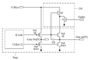
도 4는 본 발명의 제1실시예에 따른 표시장치에 적용되는 게이트 드라이버의 구성을 나타낸 예시도이며, 도 5는 본 발명에 따른 표시장치에 적용되는 신호들의 파형을 나타낸 예시도이다. 도 6a는 SLC(Simple Logic Circuit)를 기반으로 하는 스테이지를 나타낸 예시도이며, 도 6b는 HDAC(Half Dual Pull-down AC)를 기반으로 하는 스테이지를 나타낸 예시도이다. FIG. 4 is a diagram illustrating a configuration of a gate driver applied to a display device according to a first embodiment of the present invention, and FIG. 5 is a diagram illustrating waveforms of signals applied to a display device according to the present invention. FIG. 6A is a diagram illustrating a stage based on a SLC (Simple Logic Circuit), and FIG. 6B is an example of a stage based on a HDAC (Half Dual Pull-down AC).
도 4에 도시된 게이트 드라이버(120)는 순차적으로 스캔신호들을 생성하는 스테이지들로 구성된 쉬프트 레지스터(260)를 포함한다. 각 게이트 라인들은 쉬프트 레지스터(260)의 스테이지들과 연결되어 스캔신호를 공급받는다. 게이트 드라이버(120)는, 인에이블신호라인(212)에서 인가되는 인에이블신호에 따라, 게이트 라인과 연결된 스테이지들의 출력단을 저전위 전압원(VGL 또는 Ground 등)으로 방전시키는 차단부(250)를 포함한다. 제1실시예에서, 인에이블신호는 게이트 라인과 연결된 스테이지의 출력단을 저전위 전압원(VGL, Ground)으로 방전시키는 기능을 수행하며, 이에 따라, 게이트 라인으로 공급되는 스캔신호의 출력이 제어될 수 있다. The
부연하여 설명하면, 차단부(250)에는, 게이트 라인과 연결된 스테이지의 출력단과 저전위 전압원(VGL) 사이에 연결되며, 인에이블신호라인(212)에 게이트가 연결된 트랜지스터(T3)가 구비된다. 인에이블신호에 의해 차단부(250)의 트랜지스터(T3)가 턴온 되면, 스테이지의 출력은 저전위 전압원(VGL)로 방전된다. 따라서, 스테이지가 스캔신호를 출력단으로 출력하더라도 스캔신호가 게이트 라인으로 인가되지 않는다.The blocking
제1 스테이지에서 스캔신호가 생성되어 제1 스테이지의 출력단으로 스캔신호가 출력될 때, 인에이블신호에 의해 차단부(250)의 트랜지스터(T3)가 턴오프 되면, 스캔신호는 게이트 라인으로 출력된다. 그 이후, 제2스테이지에서 스캔신호가 생성되어 제2스테이지의 출력단으로 스캔신호가 출력될 때, 인에이블신호에 의해 차단부(250)의 트랜지스터(T3)가 턴온 되면, 스캔신호는 게이트 라인으로 출력되지 못하고 저전위 전압원(VGL)의 전압이 게이트 라인으로 출력된다. When the scan signal is generated in the first stage and the scan signal is outputted to the output stage of the first stage, when the transistor T3 of the
도 4에는, 하나의 인에이블 신호를 사용하여 스캔신호의 출력을 제어하는 차단부(250)가 도시되어 있으나, 인에이블신호의 수는 이에 제한되지 않는다. 따라서, 다른 실시예들에서는, 복수의 인에이블신호라인들로부터 출력된 인에이블 신호들에 의해 차단부(250)가 구동될 수 있다. 복수의 인에이블신호를 이용하여 차단부가 동작되는 경우, 프리 차지 타임(Pre-charge time)이 늘어나, 다시 Start되는 스테이지의 출력의 특성이 더욱 좋아질 수 있다. 4, the
도 5의 Timing Diagram에 도시된 바와 같이, 첫 번째 스테이지와 두 번째 스테이지들의 스캔신호들(Gout3, Gout5)이 각 스테이지들의 출력단들로 출력될 때, 인에이블신호 라인(212)에는 게이트 오프 전압을 갖는 인에이블신호가 인가되고 있다. 따라서, 이 두 스테이지들로부터 생성된 스캔신호들은 차단부(250)를 통해 게이트 라인들에 순차적으로 출력된다. 반면에, 네 번째 스테이지와 다섯 번째 스테이지들에서 스캔신호들(Gout7, Gout9)이 각 스테이지들의 출력단들로 출력될 때, 인에이블신호 라인(212)에는 게이트 온 전압을 갖는 인에이블 신호가 인가되고 있다. 따라서, 네 번째 스테이지와 다섯 번째 스테이지들과 연결된 게이트 라인들은 차단부(250)의 트랜지스터(T3)에 의해 저전위 전압원(VGL)으로 방전된다. 즉, 게이트 오프 전압을 갖는 인에이블 신호가 인가되고 있는 구간에서는, 차단부(250)의 트랜지스터(T3)가 턴오프되며, 이에 따라, 스테이지들로부터 생성된 스캔신호들은 순차적으로 게이트 라인들로 출력된다. 따라서, 픽셀들이 데이터 라인의 데이터 전압으로 충전되는 구동영역이 생성된다. 5, when the scan signals Gout3 and Gout5 of the first stage and the second stage are output to the output stages of the stages, the enable
그러나, 게이트 온 전압을 갖는 인에이블 신호가 인가되고 있는 구간에서는, 차단부(250)의 트랜지스터(T3)가 턴온되며, 이에 따라, 스테이지들로부터 생성된 스캔신호는 게이트 라인들로 출력되지 못한다. 따라서, 픽셀들이 데이터 라인의 데이터 전압으로 충전되지 않는 구동영역이 생성된다. 인에이블신호에 의해 스테이지들로부터 생성된 스캔신호가 게이트 라인들로 출력되지 못하더라도, 스테이지로부터 생성된 캐리신호는 다음 스테이지로 전송되어 다음 스테이지들을 순차적으로 동작시킬 수 있다. However, in the section in which the enable signal having the gate-on voltage is applied, the transistor T3 of the
예를 들어, 도 5에 도시된 바와 같이, 인에이블 신호에 의해 스테이지들로부터 생성된 스캔신호가 게이트 라인들로 출력되지 못하더라도, 쉬프트 레지스터(260)의 스테이지들은 각각 캐리신호를 출력하여 다음 스테이지를 구동시킬 수 있다. 따라서, 스테이지에서 생성된 스캔신호가 게이트 라인들로 출력이 되지 않더라도, 쉬프트 레지스터의 스테이지들은 순차적으로 구동될 수 있다. For example, as shown in FIG. 5, even though the scan signal generated from the stages by the enable signal can not be output to the gate lines, the stages of the
캐리신호는 각 스테이지의 캐리신호 출력단(Carry OUT)을 통해 다음 스테이지로 공급될 수 있다. 또한, 각 스테이지는 스캔신호의 출력을 위한 풀업/풀다운 트랜지스터들 이외에 캐리신호의 출력을 위한 풀업/풀다운 트랜지스터들을 추가로 구비할 수도 있다. The carry signal may be supplied to the next stage through the carry signal output (Carry OUT) of each stage. In addition, each stage may further include pull-up / pull-down transistors for outputting a carry signal in addition to pull-up / pull-down transistors for outputting a scan signal.
여기서, 상기 쉬프트 레지스터(260)는, 도 4에 도시된 두 개의 스테이지)들 및 미도시된 복수의 스테이지들을 포함한다. 상기 스테이지들 각각은 하나의 게이트 라인과 연결되어 하나의 스캔신호를 출력할 수도 있으나, 두 개의 게이트 라인과 연결되어 두 개의 스캔신호를 순차적으로 또는 동시에 출력할 수도 있다. Here, the
부연하여 설명하면, 상기에서 설명된 스테이지들은, HDAC(half Dual pull-down AC)을 기반으로 구성될 수도 있으며, SLC(Simple Logic Circuit)를 기반으로 구성될 수 있다. 예들 들어, 도 6a에는, SLC를 기반으로 하는 스테이지가 도시되어 있으며, 도 6b에는 HDAC을 기반으로 하는 스테이지가 도시되어 있다.In other words, the above-described stages may be configured based on HDAC (half dual pull-down AC) or based on a SLC (Simple Logic Circuit). For example, in Figure 6a a stage based on SLC is shown and in Figure 6b a stage based on HDAC is shown.
우선, 도 6a를 참조하여 SLC(Simple Logic Circuit) 기반의 스테이지를 간단히 설명하면 다음과 같다. SLC 기반의 스테이지에서는, 별도의 QB-node가 없다. QB-node는 상기 게이트 오프 신호의 출력을 제어하는 노드이다.First, a simple logic circuit (SLC) -based stage will be briefly described with reference to FIG. 6A. In the SLC-based stage, there is no separate QB-node. The QB-node is a node for controlling the output of the gate-off signal.
SLC 기반의 스테이지는, 예를 들어, 7개의 TFT 및 1개의 캐패시터로 구성될 수 있다. SLC 기반의 스테이지에서는 레이아웃이 단순화될 수 있고, 베젤(Bezel)의 면적이 감소될 수 있다. The SLC-based stage may be composed of, for example, seven TFTs and one capacitor. In the SLC-based stage, the layout can be simplified and the area of the bezel can be reduced.
특히, 상기 캐패시터(CB)에 의해, 커플링 전압이 저감될 수 있고, 부스트랩(Boostrap) 전압이 증가될 수 있으며, Q 노드의 전압 Holding 특성이 향상될 수 있다. 옥사이드를 이용하는 SLC 기반의 스테이지에서는 문턱전압(Vth)의 마진 확보를 위해 상기 커패시터(CB)가 형성될 수 있으며, 이에 따라 신뢰성이 향상될 수 있다. Particularly, by the capacitor CB, the coupling voltage can be reduced, the boosting voltage can be increased, and the voltage holding characteristic of the Q node can be improved. In the SLC-based stage using oxide, the capacitor CB can be formed to secure a margin of the threshold voltage (Vth), thereby improving the reliability.
다음, 도 6b를 참조하여 HDAC(half Dual pull-down AC) 기반의 스테이지를 간단히 설명하면 다음과 같다. HDAC 기반의 스테이지는, 두 개의 QB-node를 갖고 있으며, 각 QB-node를 교번구동하기 위한 두 개의 전원을 포함한다. HDAC 기반의 스테이지에서는, pull-down TFT가 열화 및 회복을 반복하게 되므로, 회로의 신뢰성이 향상될 수 있다.Next, a stage based on a HDAC (half dual pull-down AC) will be briefly described with reference to FIG. 6B. The HDAC-based stage has two QB-nodes, and includes two power supplies to alternate each QB-node. In the HDAC-based stage, since the pull-down TFT repeats deterioration and recovery, the reliability of the circuit can be improved.
특히, HDAC 기반의 스테이지들로 구성된 게이트 드라이버에서는, 인접한 2개의 스테이지들끼리 QB-node들을 공유하고 있다. 따라서, TFT의 개수 및 회로의 사이즈가 저감될 수 있다. In particular, in a gate driver composed of HDAC-based stages, two adjacent stages share QB-nodes. Therefore, the number of TFTs and the size of the circuit can be reduced.
HDAC 기반의 스테이지에서는, 회로의 안정성이 향상될 수 있고, 회로의 신뢰성이 향상될 수 있다. In the HDAC-based stage, the stability of the circuit can be improved and the reliability of the circuit can be improved.
HDAC 기반의 스테이지에서는, 인접되어 있는 두 개의 스테이지들이 하나의 스테이지로 구현될 수도 있다. 예를 들어, 도 6b에 도시된 스테이지는, 실질적으로는, 두 개의 스테이지들을 포함한다. 부연하여 설명하면, 도 6b에 도시된 스테이지를 구성하는 두 개의 스테이지들 각각은 두 개의 QB-node를 포함하며, 상기 두 개의 스테이지들은 상기 QB-node 들을 공유한다. 이러한 형태의 스테이지는 상기한 바와 같이, HDAC(half Dual pull-down AC) 기반의 스테이지라 한다.In an HDAC-based stage, two adjacent stages may be implemented in one stage. For example, the stage shown in FIG. 6B substantially comprises two stages. In more detail, each of the two stages constituting the stage shown in FIG. 6B includes two QB-nodes, and the two stages share the QB-nodes. This type of stage is referred to as a half dual pull-down AC (HDAC) based stage, as described above.
상기한 바와 같은 본 발명에 적용되는 게이트 드라이버를 구성하는 TFT들은 산화물 TFT, 예를 들어, Indium Gallium Zinc Oxide(IGZO)로 구현될 수 있다. 그러나, 본 발명이 이에 한정되는 것은 아니다. 따라서, 본 발명에 적용되는 TFT는 아몰포스 실리콘(a-Si) TFT로 구성될 수도 있으며, 또는 LTPS 공정에 의한 폴리 TFT로 구성될 수도 있다. The TFTs constituting the gate driver applied to the present invention as described above may be implemented with an oxide TFT, for example, Indium Gallium Zinc Oxide (IGZO). However, the present invention is not limited thereto. Therefore, the TFT used in the present invention may be composed of an amorphous silicon (a-Si) TFT or a poly TFT by an LTPS process.
특히, 산화물(Oxide) TFT는 아몰포스 실리콘(a-Si) TFT 보다 전류의 이동 특성이 우수하기 때문에, 산화물 TFT가 적용되는 경우, 회로의 크기가 축소될 수 있다.Particularly, since an oxide TFT has better current transfer characteristics than an amorphous silicon (a-Si) TFT, when the oxide TFT is applied, the size of the circuit can be reduced.
또한, 산화물(Oxide) TFT의 누설전류는, a-Si TFT와 LTPS TFT 보다 낮다. 따라서, 표시장치(100)의 일부 구동영역이 다른 구동영역보다 더 낮은 프레임 속도 (Frame Rate)로 구동되도록 하는 게이트 드라이버, 또는 본 발명에 따른 표시장치에서와 같이, 일시적으로 스캔신호를 출력하지 않도록 구동되는 게이트 드라이버에, 산화물 TFT가 적용되면, 게이트 드라이버가 보다 더 안정적으로 구동될 수 있다. Further, the leakage current of the oxide TFT is lower than that of the a-Si TFT and the LTPS TFT. Therefore, as in the case of a gate driver in which a part of the driving area of the
그러나, 상기한 바와 같이, 본 발명에는, 산화물 TFT뿐만 아니라, a-Si TFT 또는 LTPS TFT가 적용될 수 있으며, 또한, a-Si TFT, LTPS TFT, Oxide TFT가 혼용될 수도 있다.However, as described above, an a-Si TFT or an LTPS TFT, as well as an oxide TFT, may be applied to the present invention, and an a-Si TFT, an LTPS TFT, and an oxide TFT may be mixed.
도 7은 본 발명에 따른 표시장치에서 구동방법을 설명하기 위한 예시도이다. 7 is an exemplary diagram for explaining a driving method in a display device according to the present invention.
본 발명에 따른 표시장치에서, 인에이블 신호를 이용하여 화면을 분할하여 동작할 시에, 동일한 스테이지의 출력이 제한 되고 동일한 스테이지에서부터 스캔신호가 출력되는 동작이, 수 프레임 동안 반복될 경우, 이런 스테이지의 트랜지스터들이 열화가 가속될 수 있다. 따라서, 본 발명에 따른 표시장치는 인에이블신호의 타이밍을 조절 하여, 스캔신호의 출력이 제한되는 스테이지가 변화되도록 패널을 조절할 수 있다. 예를 들어, 1프레임기간에서는 도 7의 (a)에 도시된 스타트(Start) 위치로부터 스탑(Stop) 위치까지 영상이 출력될 수 있으며, 2프레임기간에서는 (b)에 도시된 바와 같이 상기 스타트 위치 및 상기 스탑 위치가 상기 패널(100)의 하단 방향으로 조금 이동될 수 있다. In the display device according to the present invention, when an operation in which the output of the same stage is limited and the scan signal is output from the same stage is repeated for several frames when the screen is divided and operated using the enable signal, The deterioration of the transistors of the transistor can be accelerated. Therefore, the display apparatus according to the present invention can adjust the timing of the enable signal, and adjust the panel so that the stage where the output of the scan signal is restricted is changed. For example, in one frame period, an image may be output from the start position to the stop position shown in FIG. 7A. In the two-frame period, as shown in FIG. 7B, Position and the stop position can be slightly moved toward the lower end of the
상기에서 설명된 바와 같이, 본 발명에서는 상기 게이트 라인으로 스캔신호가 출력되고 있는지의 여부와 상관없이, 데이터 전압은 지속적으로 데이터 라인들을 통해 출력될 수 있다.As described above, in the present invention, regardless of whether a scan signal is output to the gate line, the data voltage can be continuously output through the data lines.
따라서, 상기 스타트 위치를 상기 패널(100)의 상단으로부터, (a)에 도시된 위치 및 (b)에 도시된 위치를 거쳐 상기 패널(100)의 하단으로 변경시켜 가는 것에 의해, 특정 스테이지의 열화가 방지될 수 있다. 인에이블신호의 타이밍 및 인가기간을 조절하여 화면에서 구동이 일시적으로 멈추는 구역을 수시로 변경하는 것은, TFT Backplane을 구성하고 있는 소자(a-Si, Oxide 또는 LTPS)의 특성을 고려하여 다양하게 설정될 수 있다. Therefore, by changing the start position from the upper end of the
도 8은 본 발명에 따른 표시장치에 적용되는 노드 제어부의 구성을 나타낸 예시도이다.8 is a diagram illustrating a configuration of a node control unit applied to a display device according to the present invention.
본 발명은, 도 7에 도시된 바와 같은 구동방법을 이용하여, 특정 스테이지의 소자열화 문제를 해결할 수 있다.The present invention can solve the element deterioration problem of a specific stage by using the driving method as shown in Fig.
또한, 본 발명은, 도 8에 도시된 바와 같은 노드 제어부를 이용하여, 각 스테이지를 안정적으로 구동시킬 수도 있다. Further, in the present invention, each stage can be stably driven by using a node control unit as shown in Fig.
예를 들어, 상기한 바와 같이, 게이트 구동부는 복수의 스테이지를 구비하며, 스테이지들 각각은 복수의 TFT들로 구성된다. 이 경우, 스테이지는 자신과 접속된 게이트 라인의 전압을 안정적으로 유지해야 한다. 그러나, 게이트 드라이버가 구동되는 중에, 스테이지 내의 일부 노드(node)들은 플로팅 상태가 될 수 있고, 이러한 노드들은 외부 노이즈에 의해 영향을 받을 수 있으며, 이에 따라, 게이트 라인의 전압이 변화되는 등의 비정상적인 구동이 초래될 수 있다. For example, as described above, the gate driver has a plurality of stages, and each of the stages is composed of a plurality of TFTs. In this case, the stage must stably maintain the voltage of the gate line connected thereto. However, during the operation of the gate driver, some of the nodes in the stage may become floating, and these nodes may be affected by external noise, thereby causing abnormalities such as a change in the voltage of the gate line Driving can be caused.
또한, 스테이지에 포함된 TFT들은 플로팅 상태의 노드들에 남아있는 잔류 전하에 의한 스트레스로 인해 수명이 단축될 수 있다. 특히, 산화물 반도체를 사용하는 TFT의 경우 오프 전류(off current)가 매우 낮기 때문에, 잔류 전하가 자연적으로 방전되기 까지 매우 긴 시간이 필요하다. 따라서, 산화물 반도체를 사용하는 TFT가 잔류 전하에 의한 스트레스를 받는 시간 또한 길어진다. Further, the TFTs included in the stage can be shortened in life due to the stress due to the residual charge remaining in the nodes in the floating state. Particularly, in the case of a TFT using an oxide semiconductor, since the off current is very low, a very long time is required until the residual charge is naturally discharged. Therefore, the time for which the TFT using the oxide semiconductor is subjected to the stress due to the residual charge also becomes longer.
따라서, 본 발명은, 도 8에 도시된 바와 같이, 각 스테이지에 노드 제어부(24)를 추가하여, 플로팅 노드를 특정 상태로 제어함과 동시에 잔류 전하를 최소화한다. 이로 인해, 게이트 드라이버가 더욱 안정적으로 구동될 수 있으며, 게이트 드라이버를 구성하는 트랜지스터들의 수명과 신뢰성이 증가될 수 있다. 이 경우, 도 8에 도시된 구동부(22)는, 풀업트랜지스터(Tpu) 또는 풀다운 트랜지스터(Tpd)를 구동하는 신호를 생성하는 기능을 수행하며, 예를 들어, 도 6a 및 도 6b에 도시된 바와 같은 영역을 포함할 수 있다.Therefore, in the present invention, as shown in Fig. 8, the
본 발명에 의하면, 게이트 드라이버는, 노드 제어부(24)를 이용하여 플로팅 노드를 특정 상태로 제어하고, 이에 따라 노이즈와 무관하게 게이트 라인의 전압이 안정화될 수 있다. 또한, 본 발명은 노드 제어부(24)를 이용하여 풀업 트랜지스터 및 풀다운 트랜지스터를 일정시간 동안 턴-오프시킬 수 있고, 이에 따라 TFT의 수명과 신뢰성을 향상시킬 수 있다. 또한, 본 발명은 파워 공급이 중단될 때 노드 제어부(24)를 이용하여 잔류 전하를 제거함으로써 TFT의 수명을 향상시킬 수 있다. According to the present invention, the gate driver controls the floating node to a specific state by using the node control section (24), so that the voltage of the gate line can be stabilized irrespective of the noise. Further, the present invention can turn off the pull-up transistor and the pull-down transistor for a predetermined time using the
특히, 상기 노드 제어부(24)에 의해, 게이트 라인의 전압이 안정화될 수 있기 때문에, 본 발명의 다양한 실시예들에서, 스캔신호가 게이트 라인으로 출력되지 않는 기간에도, 게이트 라인의 전압이 안정화될 수 있다. In particular, since the voltage of the gate line can be stabilized by the
부연하여 설명하면, 이하에서 설명되는 노드 제어부(24)는, 이하에서 설명될 본 발명에 적용되는 각각의 스테이지에 적용될 수 있으며, 이에 따라, 스캔신호가 게이트 라인으로 출력되지 않는 기간에도, 게이트 라인의 전압이 안정화될 수 있다. The
상기 노드 제어부(24)로 입력되는 제어신호(CS)는 상기 스테이지의 구조 및 기능에 따라, 다양한 타이밍에 상기 노드 제어부(24)로 입력될 수 있다. The control signal CS input to the
우선, 도 8을 참조하면, 본 발명에 적용되는 스테이지는 풀업 트랜지스터(Tpu), 풀다운 트랜지스터(Tpd), 구동부(22) 및 노드제어부(24)를 포함한다. 풀업 트랜지스터(Tpu)는 제1신호라인과 출력단자(20) 사이에 접속된다. 여기서, 제1신호라인으로는 클럭(CLK) 또는 고전위 전압(VDD)이 공급될 수도 있다. 풀업 트랜지스터(Tpu)의 게이트는 제1노드(N1), 즉, Q노드에 접속된다. 풀업 트랜지스터(Tpu)는 제1노드(N1)의 전압에 따라, 고전위 전압(VDD)을 출력단자(20)로 공급한다. 8, the stage to which the present invention is applied includes a pull-up transistor Tpu, a pull-down transistor Tpd, a
풀다운 트랜지스터(Tpd)는 저전위 전압(VSS)을 공급하는 제2신호라인과 출력단자(20) 사이에 접속된다. 그리고, 풀다운 트랜지스터(Tpd)의 게이트는 제2노드(N2), 즉, QB노드에 접속된다. 풀다운 트랜지스터(Tpd)는 제2노드(N2)의 전압에 따라, 저전위 전압(VSS)을 출력단자(20)로 공급한다.The pull-down transistor Tpd is connected between the second signal line supplying the low potential voltage VSS and the
구동부(22)는 하나 이상의 신호라인들(미도시)로부터 공급되는 신호들에 따라, 제1노드(N1) 및 제2노드(N2)의 전압을 제어한다. 구동부(22)는 제1노드(N1) 및 제2노드(N2)의 전압을 제어하면서 풀업 트랜지스터(Tpu) 및 풀다운 트랜지스터(Tpd)를 교번적으로 턴-온 및 턴-오프할 수 있다. The driving
구동부(22)와는 별개로, 노드 제어부(24)도 제1노드(N1), 제2노드(N2) 및 출력단자(20)의 전압을 제어한다. 예를 들어, 노드제어부(24)는 제어신호(CS)에 따라, 제1노드(N1), 제2노드(N2) 및 출력단자(20)로 소정의 전압, 예를 들어 저전위 전압(VSS)을 공급할 수 있다. The
제1노드(N1), 제2노드(N2)로 저전위 전압(VSS)이 공급되면, 풀업 트랜지스터(Tpu) 및 풀다운 트랜지스터(Tpd)가 턴-오프 상태로 설정된다. 그리고, 출력단자(20)로 저전위 전압원의 전압이 공급되면 출력단자(20)는 저전위 전압(VSS)을 유지하게 된다. When the low potential voltage VSS is supplied to the first node N1 and the second node N2, the pull-up transistor Tpu and the pull-down transistor Tpd are set to the turn-off state. When the voltage of the low potential voltage source is supplied to the
상기 노드 제어부(24)는 제1트랜지스터(T1) 내지 제3트랜지스터(T3)를 구비한다.The
제1트랜지스터(T1)는 제1노드(N1)와 저전위 전압원 사이에 접속되고, 제2트랜지스터(T2)는 제2노드(N2)와 저전위 전압원 사이에 접속된다. 제3트랜지스터(T3)는 출력단자(20)와 저전위 전압원 사이에 접속된다. 노드제어부(24)의 제1트랜지스터(T1), 제2트랜지스터(T2) 및 제3트랜지스터(T3)는 제어신호(CS)에 따라 턴-온 또는 턴-오프된다. The first transistor T1 is connected between the first node N1 and the low potential voltage source and the second transistor T2 is connected between the second node N2 and the low potential voltage source. The third transistor T3 is connected between the
제어신호(CS)는, 저전위 전압(VSS), 고전위 전압(VDD), 고전위 전압(VDD) 이상의 전압 또는 저전위 전압(VSS)과 고전위 전압(VDD) 사이의 소정의 전압으로 설정될 수 있다. The control signal CS is set to a voltage equal to or higher than the low potential voltage VSS, the high potential voltage VDD and the high potential voltage VDD or the predetermined voltage between the low potential voltage VSS and the high potential voltage VDD .
부연하여 설명하면, 상기 노드 제어부(24)는, 제어신호(CS)에 따라, 플로팅 상태로 유지되는 상기 제1노드 또는 상기 제2노드로 저전위 전압(VSS)을 공급하며, 이에 따라, 상기 제1노드 또는 상기 제2노드로 비정상적인 신호가 공급되는 현상이 방지될 수 있다.The
상기에서 설명된 본 발명에서는, 스캔신호가 게이트 라인으로 출력되는 것을 제어함으로써, 스테이지의 일부 노드들이 더 긴 시간 동안 플로팅되어, 트랜지스터가 잔류전하에 의해 열화 되는 것이 완화될 수 있다.In the present invention described above, by controlling the scan signal to be output to the gate line, some nodes of the stage can be floated for a longer time, so that deterioration of the transistor by the residual charge can be mitigated.
또한, 상기 설명에서는, 상기 노드 제어부(24)가 상기 풀업 트랜지스터(Tpu)와 연결된 제1노드(N1) 또는 상기 풀다운 트랜지스터(Tpd)와 연결된 제2노드(N2)에 연결된 것으로 설명되었다. 그러나, 상기 노드 제어부(24)는 상기 제1노드 및 상기 제2노드 이외에도, 플로팅 상태로 유지되는 노드들에 연결되어, 플로팅된 노드에 특정 전압을 공급할 수 있으며, 이에 따라, 스테이지를 구성하는 노드들 중, 플로팅된 노드로 비정상적인 신호가 공급되는 현상이 방지될 수 있다. 이에 따라, 게이트 라인의 전압이 안정적으로 유지될 수 있다.Also, in the above description, it has been described that the
부연하여 설명하면, 상기 노드 제어부(24)는 본 발명의 각 실시예에 적용되는 스테이지에 구비될 수 있으며, 이에 따라, 스테이지가 안정적으로 구동될 수 있다. In other words, the
도 9는 본 발명에 따른 표시장치를 안정적으로 구동시키기 위한 구동방법을 설명하기 위한 예시도이다.9 is an exemplary diagram for explaining a driving method for stably driving the display device according to the present invention.
본 발명에 적용되는 상기 게이트 드라이버의 구동시간이 증가 할수록 PBTS가 증가 하여, Pull down TFT의 문턱전압(Vth)이 쉬프트(Shift)될 수 있다. As the driving time of the gate driver applied to the present invention increases, the PBTS increases and the threshold voltage (Vth) of the pull-down TFT can be shifted.
상기한 바와 같은 문턱전압의 쉬프트를 방지하기 위해, 도 9에 도시된 바와 같이, VSS_2의 값을 낮추어 주는 방법이 이용될 수 있다. In order to prevent the shift of the threshold voltage as described above, a method of lowering the value of VSS_2 may be used, as shown in FIG.
부연하여 설명하면, 도 9의 (a)는, 풀다운 트랜지스터의 문턱전압이 쉬프트됨에 따라, 인에이블신호에 의해 스캔신호가 출력되지 않는 기간에서 비정상적인 형태로 출력되고 있는 스캔신호를 나타낸다. More specifically, FIG. 9A shows a scan signal which is outputted in an abnormal form during a period in which the scan signal is not output by the enable signal as the threshold voltage of the pull-down transistor is shifted.
예를 들어, 본 발명에서는, 인에이블신호에 의해 스캔신호가 출력되지 않는 기간에서, 스캔신호가 출력되지 않는다. 그러나, 풀다운 트랜지스터의 문턱전압이 쉬프트되면, 도 9의 (a)에 도시된 바와 같이, 상기 기간에, 비정상적인 형태의 스캔신호가 출력될 수 있다.For example, in the present invention, the scan signal is not output in a period in which the scan signal is not output by the enable signal. However, if the threshold voltage of the pull-down transistor is shifted, an abnormal type of scan signal may be output during the period as shown in Fig. 9 (a).
이를 방지하기 위해, 본 발명에서는, 도 9의 (b)에 도시된 바와 같이, 게이트 라인과 연결되어 있는 출력단에, 게이트 오프 신호로 출력되는 VSS보다 더 낮은 값을 갖는 VSS_2가 연결될 수 있다. 예를 들어, 인에이블신호에 의해 스캔신호가 출력되지 않는 기간에서, 출력단에 연결된 트랜지스터가 턴온되면, VSS_2가 게이트 오프 신호로 출력된다. 따라서, 인에이블신호에 의해 스캔신호가 출력되지 않는 기간에서, 비정상적인 형태의 스캔신호가 출력되지 않는다. To prevent this, in the present invention, as shown in FIG. 9B, VSS_2 having a value lower than VSS outputted as a gate off signal may be connected to an output terminal connected to the gate line. For example, when the transistor connected to the output terminal is turned on in a period in which the scan signal is not output by the enable signal, VSS_2 is output as the gate off signal. Therefore, in a period in which the scan signal is not output by the enable signal, the abnormal scan signal is not output.
도 10은 본 발명에 따른 표시장치를 안정적으로 구동시키기 위한 안정화 회로의 구성을 나타낸 예시도이다. 10 is an exemplary view showing a configuration of a stabilization circuit for stably driving the display device according to the present invention.
본 발명에 따른 표시장치를 안정적으로 구동시키기 위해, 도 9의 (b)에 도시된 바와 같은 방법이 적용될 수 있으며, 도 9의 (b)에 도시된 방법을 실행시키기 위한 구체적인 방법이 도 10에 도시되어 있다.In order to stably drive the display device according to the present invention, a method as shown in Fig. 9B can be applied, and a specific method for executing the method shown in Fig. 9B is shown in Fig. 10 Respectively.
본 발명에서, 스테이지의 출력단은, 인에이블 신호에 의해 스캔신호가 출력되지 않을 때, 도 10에 도시된 바와 같은 안정화 회로(25)에 의해 로우 레벨로 풀 다운될 수 있으며, 이에 따라, 로우 레벨을 갖는 게이트 오프 신호가 안정적으로 출력될 수 있다. In the present invention, the output stage of the stage can be pulled down to the low level by the
예를 들어, 인에이블신호에 의해 스캔신호가 출력되지 않는 기간에, 스테이지의 Q노드는 로우신호를 출력하며, 출력단(gate out(N))은 로우신호를 갖는 게이트 오프신호를 출력한다.For example, during a period in which the scan signal is not output by the enable signal, the Q node of the stage outputs a low signal and the output terminal (gate out (N)) outputs a gate off signal having a low signal.
이 경우, 게이트가 Q노드와 연결된 제1트랜지스터(T1)는 턴오프된다. 또한, 스테이지에서 스캔신호로 이용될 클럭이 입력되는 단자와 상기 제1트랜지스터(T1)와 연결되어 있으며, 상기 단자에 게이트가 연결되어 있는 제2트랜지지스터(T2)는, 상기 클럭이 하이신호임으로, 상기 클럭에 의해 턴온된다. 따라서, 상기 단자와 상기 출력단에 연결되어 있으며, 게이트가 상기 제1트랜지스터와 제2트랜지스터의 연결단에 연결되어 있는 제3트랜지스터(T3)는 턴온된다. 이에 따라, 상기 출력단 및 저전위 전압원에 연결되어 있으며, 게이트가 상기 제3트랜지스터(T3)와 연결된 제4트랜지스터(T4)가 턴온되어, 게이트 오프 신호보다 낮은 레벨의 전압이, 게이트 라인으로 출력된다. In this case, the first transistor T1 whose gate is connected to the Q node is turned off. The second transcaster T2 is connected to the first transistor T1 through a terminal to which a clock to be used as a scan signal is input in the stage and to which a gate is connected. And is turned on by the clock. Accordingly, the third transistor T3, which is connected to the terminal and the output terminal, and whose gate is connected to the connection node between the first transistor and the second transistor, is turned on. Accordingly, the fourth transistor T4 whose gate is connected to the third transistor T3 is turned on, and a voltage lower than the gate-off signal is output to the gate line .
따라서, 인에이블신호에 의해 스캔신호가 출력되지 않는 구간에서, 도 9의 (a)에 도시된 바와 같은 비정상적인 형태의 스캔신호가 출력되지 않는다.Therefore, in the section where the scan signal is not output by the enable signal, the abnormal scan signal as shown in FIG. 9A is not output.
그러나, 스캔신호가 정상적으로 출력되는 구간에서는, 상기 클럭이, 제1트랜지스터(T1)와 제2트랜지스터(T2)를 통해 방전되기 때문에, 제4트랜지스터(T4)가 턴오프되며, 이에 따라, 게이트 오프 신호보다 낮은 레벨의 전압이 게이트 라인으로 출력되지 않는다. However, since the clock is discharged through the first transistor T1 and the second transistor T2 in the period in which the scan signal is normally output, the fourth transistor T4 is turned off, A voltage lower than the signal is not output to the gate line.
도 11은 본 발명의 표시장치에 적용되는 또 다른 구조의 게이트 드라이버를 나타낸 예시도이다. 11 is an exemplary view showing a gate driver of another structure applied to the display device of the present invention.
도 11에 도시된 구조에서, 상기 게이트 드라이버(120)는, 순차적으로 상기 스캔신호들을 생성하는 복수의 스테이지들을 포함하며, 스테이지들 각각에는, 도 11에 도시된 바와 같이, 차단부(250)가 연결된다. 스테이지들에 연결되어 있는 차단부(250)들 중 적어도 하나는, 인에이블 신호에 따라, 상기 스테이지로부터 상기 게이트 라인으로 출력되는 스캔신호를 차단할 수 있다. In the structure shown in FIG. 11, the
즉, 상기 게이트 드라이버(120)에서는, 도 11에 도시된 바와 같이, 하나의 스캔신호를 출력하는 스테이지마다, 하나의 차단부(250)가 개별적으로 연결된다.That is, in the
예를 들어, 상기 차단부(250)는, 도 11에 도시된 바와 같이, 클럭(CLK)이 입력되는 단자와 상기 스테이지의 풀업 트랜지스터(Pull up)에 연결되는 제42트랜지스터(T42), 상기 클럭이 입력되는 단자와 상기 제42트랜지스터(T42)의 게이트에 연결되며, 상기 클럭에 의해 턴온 또는 턴오프되는 제41트랜지스터 및 저전위 전압이 입력되는 단자 또는 그라운드(이하, 간단히 ‘저전위 전압원’이라 함)와, 상기 제42트랜지스터(T42)의 게이트에 연결되며, 상기 인에이블 신호(Enable)에 의해 턴온 또는 턴오프되는 제5i트랜지스터(T5i)를 포함한다.For example, as shown in FIG. 11, the
이 경우, 도 11에 도시된 상기 스테이지의 풀업 트랜지스터(Pull Up)가 턴온되고, 클럭(CLK)이 하이(High)일 때, 상기 인에이블 신호가 오프이면, 제5i트랜지스터(T5i)는 오프되고, 제41트랜지스터(T41) 및 제42트랜지스터(T42)는 턴온되어, 상기 풀업 트랜지스터로 상기 클럭이 입력되며, 상기 클럭은 상기 풀업 트랜지스터를 통해 상기 게이트 라인으로 출력된다. 즉, 상기 클럭이 스캔신호가 되어 상기 게이트 라인으로 출력된다.In this case, when the pull-up transistor of the stage shown in Fig. 11 is turned on and the clock signal CLK is high, if the enable signal is off, the fifth transistor T5i is turned off The 41st transistor T41 and the 42nd transistor T42 are turned on, the clock is input to the pull-up transistor, and the clock is output to the gate line through the pull-up transistor. That is, the clock is a scan signal and is output to the gate line.
그러나, 상기 풀업 트랜지스터가 턴온되고, 상기 클럭이 하이(High)일 때, 상기 인에이블 신호가 온되면, 제41트랜지스터(T41) 및 제5i트랜지스터(T5i)가 턴온된다. 이에 따라, 상기 클럭은 상기 제41트랜지스터(T41) 및 상기 제5i트랜지스터(T5i)를 통해 저전위 전압원으로 방전된다. 따라서, 상기 클럭이 상기 풀업 트랜지스터를 통해 상기 게이트 라인으로 출력되지 않는다. 즉, 상기 게이트 라인으로 스캔신호가 출력되지 않는다.However, when the pull-up transistor is turned on and the clock is high, the 41st transistor T41 and the 5i th transistor T5i are turned on when the enable signal is turned on. Accordingly, the clock is discharged to the low potential voltage source through the forty-first transistor T41 and the fifth transistor T5i. Therefore, the clock is not output to the gate line through the pull-up transistor. That is, no scan signal is output to the gate line.
상기한 바와 같이, 각각의 스테이지에서 상기 인에이블 신호를 제어하는 것에 의해, 상기 스캔신호의 출력여부가 결정될 수 있다. As described above, whether to output the scan signal can be determined by controlling the enable signal in each stage.
부연하여 설명하면, 도 11에 도시된 구조에서는, 도4를 참조하여 설명한 구조와는 달리, 스테이지에서 출력되는 스캔신호의 출력을 풀다운 시키는 방법이 아닌, 스테이지의 풀업 트랜지스터로 공급되는 클럭을 제어하여, 스캔신호의 출력여부를 제어하는 방법을 이용하고 있다. 우선, 기본 정상 구동 시에는 Enable 신호가 Low로 되어 T5i가 OFF 되고, T41을 통해 전송된 하이레벨의 클럭이 T42를 턴온시킨다. T42가 턴온되면, 클럭이 T42를 통해 Pull up Tr로 전송되며, 이에 따라, 정상적인 스캔신호가 출력단을 통해 게이트 라인으로 출력된다. Stop 동작 시에는 Enable 신호가 T5i를 턴온시켜, T42의 Gate를 Low레벨로 Pull down 시킨다. 따라서 클럭(CLK)이 T42를 통해 Pull up Tr로 출력되지 못하고, 결국 게이트 라인으로 스캔신호가 츨력되지 않는다. In other words, unlike the structure described with reference to FIG. 4, in the structure shown in FIG. 11, the clock supplied to the pull-up transistor of the stage is controlled not by pulling down the output of the scan signal output from the stage , And a method of controlling whether the scan signal is output or not is used. At the time of the normal normal operation, the Enable signal becomes Low, T5i is turned off, and the high level clock transmitted through T41 turns on T42. When the transistor T42 is turned on, the clock is transmitted through the transistor T42 to the pull-up transistor Tr, so that the normal scan signal is output to the gate line through the output terminal. In stop operation, enable signal turns on T5i and pulls down gate of T42 to low level. Therefore, the clock (CLK) can not be output to the pull-up Tr through T42, and the scan signal is not output to the gate line after all.
도 12는 본 발명의 표시장치에 적용되는 또 다른 구조의 게이트 드라이버를 나타낸 예시도이다. 12 is an exemplary view showing a gate driver of another structure applied to the display device of the present invention.
도 12에 도시된 구조에서, 게이트 드라이버(120)는 순차적으로 스캔신호들을 생성하는 복수의 스테이지들을 포함하며, 상기 스테이지들 각각에는 차단부(250)가 연결된다. 상기 차단부들 중 적어도 하나는, 인에이블신호에 따라, 상기 스테이지로부터 상기 게이트 라인으로 출력되는 스캔신호를 차단할 수 있다. In the structure shown in FIG. 12, the
도 12에 도시된 게이트 드라이버(120)의 기본적인 구조는, 본 발명의 도 11을 참조하여 설명된 게이트 드라이버의 기본적인 구조와 유사하다. 즉, 도 12에 도시된 바와 같이, 하나의 스캔신호를 출력하는 스테이지마다, 하나의 차단부(250)가 개별적으로 연결된다. 하지만, 이전 실시예와는 다른 구조의 차단부(250)가 구비된다.The basic structure of the
예를 들어, 상기 차단부(250)는, 도 12에 도시된 바와 같이, 클럭(CLK)이 입력되는 단자와 상기 스테이지의 풀업 트랜지스터(Pull up)에 연결되며, 상기 클럭에 의해 턴온 또는 턴오프되는 제41트랜지스터(T41) 및 저전위 전압이 입력되는 저전위 전압원과, 상기 스테이지의 풀업 트랜지스터(Pull up)에 연결되며, 상기 인에이블 신호(Enable)에 의해 턴온 또는 턴오프되는 제5i트랜지스터(T5i)를 포함한다.For example, as shown in FIG. 12, the
이 경우, 도 12에 도시된 상기 스테이지의 풀업 트랜지스터(Pull Up)가 턴온되고, 클럭(CLK)이 하이(High)일 때, 상기 인에이블 신호가 오프이면, 제5i트랜지스터(T5i)는 오프되고, 제41트랜지스터(T41)는 턴온되어, 상기 풀업 트랜지스터로 상기 클럭이 입력되며, 상기 클럭은 상기 풀업 트랜지스터를 통해 상기 게이트 라인으로 출력된다. 즉, 상기 클럭이 스캔신호가 되어 상기 게이트 라인으로 출력된다.In this case, when the pull-up transistor of the stage shown in FIG. 12 is turned on and the clock signal CLK is high, if the enable signal is off, the fifth transistor T5i is turned off , The 41st transistor T41 is turned on, the clock is input to the pull-up transistor, and the clock is output to the gate line via the pull-up transistor. That is, the clock is a scan signal and is output to the gate line.
그러나, 상기 풀업 트랜지스터가 턴온되고, 상기 클럭이 하이(High)일 때, 상기 인에이블 신호가 온되면, 제41트랜지스터(T41) 및 제5i트랜지스터(T5i)가 턴온된다. 이에 따라, 상기 클럭은 상기 제41트랜지스터(T41) 및 상기 제5i트랜지스터(T5i)를 통해 방전된다. 따라서, 상기 클럭이 상기 풀업 트랜지스터를 통해 상기 게이트 라인으로 출력되지 않는다. 즉, 상기 게이트 라인으로 스캔신호가 출력되지 않는다.However, when the pull-up transistor is turned on and the clock is high, the 41st transistor T41 and the 5i th transistor T5i are turned on when the enable signal is turned on. Accordingly, the clock is discharged through the forty-first transistor T41 and the fifth transistor T5i. Therefore, the clock is not output to the gate line through the pull-up transistor. That is, no scan signal is output to the gate line.
상기한 바와 같이, 각각의 스테이지에서 상기 인에이블 신호를 제어하는 것에 의해, 상기 스캔신호의 출력여부가 결정될 수 있다.As described above, whether to output the scan signal can be determined by controlling the enable signal in each stage.
부연하여 설명하면, 도 12에 도시된 게이트 드라이버는, 도 11에 도시된 구조에서 T42가 제거되고, T41이 직접 풀업 트랜지스터에 연결된 경우와 유사한 구조를 가지고 있다. 도 12에 도시된 게이트 드라이버는, Stop & start 동작을 하기 위해, T41을 통해 들어오는 clock을, 도 11에 도시된 게이트 드라이버와 마찬가지로 Enable 신호를 이용하여 Low level로 만든다. 이에 따라, clock이 Pull up TFT를 통해 gate line으로 출력되지 못한다.To be more specific, the gate driver shown in Fig. 12 has a structure similar to the case where T42 is removed in the structure shown in Fig. 11, and T41 is directly connected to the pull-up transistor. The gate driver shown in FIG. 12 makes the clock coming in through T41 to a Low level by using an enable signal in the same way as the gate driver shown in FIG. 11 in order to perform a stop & start operation. As a result, the clock can not be output to the gate line through the pull-up TFT.
도 13은 본 발명의 표시장치에 적용되는 또 다른 구조의 게이트 드라이버를 나타낸 예시도이다.13 is an exemplary view showing a gate driver of another structure applied to the display device of the present invention.
본 실시예에서, 게이트 드라이버(120)는, 도 13에 도시된 바와 같이, 순차적으로 상기 스캔신호들을 생성하는 복수의 스테이지들을 포함하며, 상기 스테이지들 각각에는 차단부(250)가 연결된다. 상기 차단부(250)들 중 적어도 하나는, 인에이블 신호에 따라, 상기 스테이지로부터 상기 게이트 라인으로 출력되는 스캔신호를 차단할 수 있다.In this embodiment, the
게이트 드라이버(120)의 기본적인 구조는, 도 11 및 도 12를 참조하여 설명된 본 발명의 제2실시예에 적용되는 게이트 드라이버의 기본적인 구조와 유사하다. 즉, 도 13에 도시된 바와 같이, 하나의 스캔신호를 출력하는 스테이지마다, 하나의 차단부(250)가 개별적으로 연결된다.The basic structure of the
예를 들어, 상기 차단부(250)는, 도 13에 도시된 바와 같이, 클럭(CLK)이 입력되는 단자와 상기 스테이지의 풀업 트랜지스터(Pull up)에 연결되며, 게이트가 상기 풀업 트랜지스터의 게이트에 연결되어 있는 제42트랜지스터(T42) 및 저전위 전압이 입력되는 저전위 전압원과, 상기 스테이지의 풀업 트랜지스터에 연결되며, 상기 인에이블 신호(Enable)에 의해 턴온 또는 턴오프되는 제5i트랜지스터(T5i)를 포함한다.For example, as shown in FIG. 13, the blocking
이 경우, 도 13에 도시된 상기 스테이지의 풀업 트랜지스터(Pull Up)가 턴온되고, 클럭(CLK)이 하이(High)일 때, 상기 인에이블 신호가 오프이면, 제5i트랜지스터(T5i)는 오프되고, 제42트랜지스터(T42)는 턴온되어, 상기 풀업 트랜지스터로 상기 클럭이 입력되며, 상기 클럭은 상기 풀업 트랜지스터를 통해 상기 게이트 라인으로 출력된다. 즉, 상기 클럭이 스캔신호가 되어 상기 게이트 라인으로 출력된다.In this case, when the pull-up transistor of the stage shown in FIG. 13 is turned on and the clock signal CLK is high, if the enable signal is off, the fifth transistor T5i is turned off , The 42nd transistor T42 is turned on, the clock is input to the pull-up transistor, and the clock is output to the gate line via the pull-up transistor. That is, the clock is a scan signal and is output to the gate line.
그러나, 상기 풀업 트랜지스터가 턴온되고, 상기 클럭(CLK)이 하이(High)일 때, 상기 인에이블 신호가 턴온되면, 제42트랜지스터(T42)가 턴온된다. 이에 따라, 상기 클럭은 상기 제42트랜지스터(T42) 및 상기 제5i트랜지스터(T5i)를 통해 저전위 전압원으로 방전된다. 따라서, 상기 클럭이 상기 풀업 트랜지스터를 통해 상기 게이트 라인으로 출력되지 않는다. 즉, 상기 게이트 라인으로 스캔신호가 출력되지 않는다.However, when the pull-up transistor is turned on and the clock (CLK) is high, when the enable signal is turned on, the forty-second transistor (T42) is turned on. Accordingly, the clock is discharged to the low potential voltage source through the forty-second transistor T42 and the fifth transistor T5i. Therefore, the clock is not output to the gate line through the pull-up transistor. That is, no scan signal is output to the gate line.
부연하여 설명하면, 도 13에 도시된 게이트 드라이버에서는, T42 의 gate가 스테이지의 Q-node에 연결된다. 따라서, 정상 화면 구동 시에, Q-node가 high 전압이면, 하이레벨을 갖는clock이 Pull up TFT를 통해 gate line으로 출력되며, Q-node가 low 전압일 때에는 T42가 OFF되어, 클럭이 게이트 라인으로 출력되지 않는다. 또한, 도 13에 도시된 게이트 드라이버에서는, Stop & Start 동작 시에는, Enable 신호가 High로 되어, T5i가 On되며, 따라서, T42를 통과한 clock은 저전위 전압원으로 방전된다. 따라서, gate line으로 스캔신호가 출력되지 않아, gate line으로 스캔신호 출력이 Stop된다.In more detail, in the gate driver shown in FIG. 13, the gate of T42 is connected to the Q-node of the stage. Therefore, when the Q-node is high voltage, the high-level clock is output to the gate line through the pull-up TFT. When the Q-node is low, T42 is turned off, . In the gate driver shown in FIG. 13, in the Stop & Start operation, the Enable signal becomes High and T5i is On, and therefore the clock passing through T42 is discharged to the low potential voltage source. Therefore, the scan signal is not output to the gate line, and the scan signal output to the gate line is stopped.
도 11 내지 도 13에 도시된 게이트 드라이버의 구조들에서, 상기 인에이블 신호에 의한 스탑(Stop) 동작 시에 플로팅(Floating)된 게이트 라인은, 도 8을 참조하여 설명한 안정화 회로(24)에 의해 안정화될 수 있다. In the structures of the gate driver shown in Figs. 11 to 13, the floating gate line at the time of the stop operation by the enable signal is supplied to the
도 14는 본 발명의 표시장치에 적용되는 또 다른 구조의 게이트 드라이버를 나타낸 예시도이고, 도 15 내지 도 18은 도 14의 도시된 게이트 드라이버를 구성하는 스테이지의 다양한 구성도들이다. Fig. 14 is an exemplary view showing a gate driver of another structure applied to the display device of the present invention, and Figs. 15 to 18 are various constructions of stages constituting the gate driver shown in Fig.
도 14에 도시된 바와 같이, 게이트 드라이버(120)는 순차적으로 캐리신호들(Carry_Out_1 to Carry_Out_7)을 생성하는 캐리스테이지(1st stage)들을 포함하는 제1쉬프트 레지스터(270) 및 상기 캐리신호들에 따라, 순차적으로 상기 스캔신호들(Gate_Out_1 to Gate_Out_7)을 상기 게이트 라인들로 출력하는 스캔스테이지(2nd stage)들을 포함하는 제2쉬프트 레지스터(280)를 포함하며, 상기 제2쉬프트 레지스터(280)에 포함되어 있는 상기 스캔스테이지(2nd stage)들 중 적어도 하나는, 상기 인에이블신호(Enable)에 따라, 상기 게이트 라인으로 출력되는 스캔신호를 차단한다. As shown in FIG. 14, the
예를 들어, 도 14에서 좌측에 형성되어 있는 캐리스테이지(1st stage)들은 제1쉬프트 레지스터(270)를 형성하며, 우측에 형성되어 있는 스캔스테이지(2nd stage)들은 제2쉬프트 레지스터(280)를 형성한다.For example, the carry stages formed on the left side in FIG. 14 form the
상기 제1쉬프트 레지스터(270)에 형성되어 있는 상기 캐리스테이지들은 순차적으로 상기 캐리신호들(Carry_Out_1 to Carry_Out_7)을 출력한다. The carry stages formed in the
상기 캐리신호는, 상기 스캔스테이지에 스타트 신호로 입력된다. 상기 캐리신호에 의해 상기 스캔스테이지가 구동되며, 상기 스캔스테이지는 최종적으로 상기 스캔신호를 상기 게이트 라인으로 출력한다. 상기 캐리신호는, 상기 제1쉬프트 레지스터(270)에 구비된 또 다른 캐리스테이지에 스타트 신호로 입력된다.The carry signal is input as a start signal to the scan stage. The scan stage is driven by the carry signal, and the scan stage finally outputs the scan signal to the gate line. The carry signal is input as a start signal to another carry stage provided in the
상기 캐리신호와 함께 상기 인에이블 신호(Enable)가 상기 스캔스테이지로 입력될 때, 상기 스캔스테이지는 상기 스캔신호를 상기 게이트 라인으로 출력하지 않을 수 있다. When the enable signal Enable is input to the scan stage together with the carry signal, the scan stage may not output the scan signal to the gate line.
즉, 상기 제2쉬프트 레지스터(280)를 구성하는 상기 스캔스테이지들은, 상기 캐리신호에 의해 구동되나, 상기 인에이블신호에 따라 상기 스캔신호를 상기 게이트 라인으로 출력하지 않을 수 있다. That is, the scan stages constituting the
부연하여 설명하면, 본 실시예는, 전술한 실시예들과는 달리, 복수의 스테이지들로 구성된 두 개의 쉬프트 레지스터들(270, 280)을 이용한 듀얼 쉬프트레지스터 구조를 가지고 있다. In other words, unlike the above-described embodiments, the present embodiment has a dual shift register structure using two
듀얼 쉬프트레지스터 구조에 적용되는 캐리스테이지들 및 스캔스테이지들은, 도 6a를 참조하여 설명된 SLC를 기반으로 구성될 수도 있으나, 도 6b를 참조하여 설명된 HDAC를 기반으로 구성될 수도 있다. Carry stages and scan stages applied to the dual shift register structure may be configured based on the SLC described with reference to FIG. 6A, but may be based on the HDAC described with reference to FIG. 6B.
듀얼 쉬프트레지스터 구조에 적용되는 상기 캐리스테이지와 상기 스캔스테이지의 세부 구성은 도 15 내지 도 18에 도시되어 있다.The detailed structure of the carry stage and the scan stage applied to the dual shift register structure is shown in FIGS. 15 to 18. FIG.
듀얼 쉬프트레지스터 구조에서 각 스테이지는, Dual Pull down GIP 구조로 구성될 수도 있으나, Simple Logic Circuit(SLC)을 기반으로 하여 구성될 수도 있으며, 또는, 불안정한 Ripple이 개선된 N-SLC(No ripple SLC)을 기반으로 하여 구성될 수 있다. SLC 기반의 듀얼 쉬프트레지스터 구조에서, Stop & Start 동작을 하기 위해서는, 도 15 내지 도 18에 도시된 바와 같이, 도 6a에 도시된 SLC기반의 스테이지에 구비된 T3c(Noise cleaner) 회로가 제거된 스테이지들이 이용되어야 하며, 스캔스테이지로는 Enable 신호가 입력되어야 한다. Each stage in the dual shift register structure may be configured with a dual pull down GIP structure, but it may be constructed based on a simple logic circuit (SLC), or a non-ripple SLC (No ripple SLC) As shown in FIG. In order to perform the Stop & Start operation in the SLC-based dual shift register structure, as shown in FIGS. 15 to 18, a stage in which the T3c (noise cleaner) circuit provided in the SLC- And an enable signal must be input to the scan stage.
예를 들어, 도 15에 도시되어 있는 바와 같이, 상기 캐리스테이지의 캐리신호(Carry Out(n))는, 상기 스캔스테이지에 입력되어 스캔스테이지를 동작시킨다. 이 경우, 일반적인 SLC기반의 스테이지에서Pre-charge TFT로 이용되는 T1의 Source에 Enable 신호가 연결된 스캔스테이지가, Enable신호에 따라 상기 스캔스테이지로부터의 스캔신호 출력을 제어하여, stop & start 동작을 한다. For example, as shown in Fig. 15, the carry signal Carry Out (n) of the carry stage is input to the scan stage to operate the scan stage. In this case, the scan stage to which the enable signal is connected to the source of T1 used as the pre-charge TFT in the general SLC-based stage controls the scan signal output from the scan stage in accordance with the Enable signal to perform the stop & start operation .
특히, 전술한 실시예들과는 달리, 본 실시예에서는, 상기 인에이블신호가 로우신호일 때, Stop & Start 동작이 실행되며, 상기 인에이블신호가 하이신호일 때, 스캔신호가 출력되는 정상 동작이 실행된다. 예를 들어, 도 15에서 상기 인에이블 신호가 하이신호이면, 상기 캐리신호(Carry Out(n))에 의해 제1트랜지스터(T1)가 턴온될 때, 상기 인에이블 신호가 상기 제1트랜지스터(T1)를 통해 전송되어, 풀업 트랜지스터(T6)가 턴온된다. 이에 따라, 상기 스캔스테이지가 스캔신호를 게이트 라인으로 출력할 수 있다. 그러나, 상기 인에이블 신호가 로우신호이면, 상기 캐리신호에 의해 상기 제1트랜지스터(T1)가 턴온되더라도, 상기 풀업 트랜지스터(T6)가 턴오프되며, 이에 따라, 상기 스캔스테이지는 스캔신호를 출력하지 않는다.Particularly, unlike the above-described embodiments, in the present embodiment, a stop & start operation is performed when the enable signal is a loud signal, and a normal operation in which a scan signal is outputted when the enable signal is a high signal is executed . For example, in FIG. 15, when the enable signal is a high signal, when the first transistor T1 is turned on by the carry signal Carry Out (n), the enable signal is supplied to the first transistor T1 , And the pull-up transistor T6 is turned on. Accordingly, the scan stage can output a scan signal as a gate line. However, if the enable signal is a low signal, even if the first transistor T1 is turned on by the carry signal, the pull-up transistor T6 is turned off so that the scan stage outputs a scan signal Do not.
또한, 도 16에 도시된 캐리스테이지와 스캔스테이지는, 도 15를 참조하여 설명된 방법과 유사한 방법으로 구동된다. 도 16에 도시된 스캔스테이지에는, 도 15에 도시된 스캔스테이지와 비교할 때, Noise cleaner회로(27)가 더 포함되어 있다. In addition, the carry stage and scan stage shown in Fig. 16 are driven in a manner similar to that described with reference to Fig. The scan stage shown in Fig. 16 further includes a noise
도 16에 도시된 스캔스테이지로 로우레벨을 갖는 인에이블신호가 입력되어, 풀업 트랜지스터(T6)가 턴오프되면, 상기 스캔스테이지로 스캔신호가 출력되지 않는다. 이 경우, T5i은 턴오프되며, 따라서, 클럭은, T42를 통해 T7n으로 전송된다. 상기 클럭은 상기 스캔스테이지의 스캔신호로 이용되기 위해 입력되는 신호이기 때문에, 상기 캐리신호가 입력될 때, 하이레벨을 갖는다. 따라서, T7n은 상기 클럭에 의해 턴온되며, 이에 따라, 스캔스테이지의 출력단으로는 저전위 전압(VSS)이 공급된다.When an enable signal having a low level is input to the scan stage shown in FIG. 16 and the pull-up transistor T6 is turned off, no scan signal is output to the scan stage. In this case, T5i is turned off, and therefore, the clock is transmitted to T7n through T42. Since the clock signal is input to be used as a scan signal of the scan stage, the clock signal has a high level when the carry signal is input. Thus, T7n is turned on by the clock, thereby supplying a low potential voltage (VSS) to the output stage of the scan stage.
따라서, 인에이블신호에 의해, 스캔신호의 출력이 제한된 경우, 스캔스테이지의 출력단에 저전위 전압(VSS)이 공급되기 때문에, 비정상적인 스캔신호가 게이트 라인으로 출력되지 않는다.Therefore, when the output of the scan signal is limited by the enable signal, the low potential voltage VSS is supplied to the output stage of the scan stage, so that an abnormal scan signal is not output to the gate line.
부연하여 설명하면, 상기 노이즈 클리너 회로(27)가 없다면, 인에이블신호에 의해 스캔신호의 출력이 제한될 때, 스캔스테이지의 출력단이 플로팅되어, 노이즈가 발생될 수 있다. 그러나, 상기 노이즈 클리너 회로(27)에 의해 저전위 전압(VSS)이 출력단에 공급되기 때문에, 게이트 라인을 통해 노이즈가 출력되지 않는다. In other words, if there is no noise
또한, 도 17에 도시된 캐리스테이지와 스캔스테이지는, 도 15를 참조하여 설명된 방법과 유사한 방법으로 구동된다. 도 17에 도시된 스캔스테이지에는, 도 15에 도시된 스캔스테이지와 비교할 때, 안정화용 트랜지스터(T9)가 더 포함되어 있으며, 상기 안정화용 트랜지스터(T9)로는 인에이블신호와 반대 극성을 갖는 반전신호(Enable_B)가 입력된다. 상기 안정화용 트랜지스터(T9)는 노드제어 트랜지스터라고도 한다.In addition, the carry stage and the scan stage shown in Fig. 17 are driven in a manner similar to the method described with reference to Fig. The scan stage shown in Fig. 17 further includes a stabilization transistor T9 as compared with the scan stage shown in Fig. 15, and the stabilization transistor T9 is provided with an inverted signal having an opposite polarity to the enable signal (Enable_B) is input. The stabilization transistor T9 is also referred to as a node control transistor.
도 17에 도시된 캐리스테이지와 스캔스테이지의 기본적인 구조 및 동작 방법은, 도 15를 참조하여 설명된 캐리스테이지와 스캔스테이지의 구조 및 동작 방법과 동일하다.The basic structure and operation method of the carry stage and the scan stage shown in FIG. 17 are the same as the structure and operation method of the carry stage and the scan stage described with reference to FIG.
그러나, 도 17에 도시된 게이트 드라이버에서는, 클럭 커플링(Clock coupling)을 방지 하기 위해, Stop & Start 동작 용 Enable 신호 외에 반전신호(Enable_B)가 추가적으로 이용되며, 반전신호에 따라 안정화용 트랜지스터(T9)가 턴온 또는 턴오프됨으로써, Stop & Start 동작 시에 Q-node가 안정화될 수 있다. However, in the gate driver shown in FIG. 17, in order to prevent clock coupling, an inverted signal (Enable_B) is additionally used in addition to an enable signal for stop & start operation, and a stabilization transistor T9 ) Is turned on or turned off, the Q-node can be stabilized in the Stop & Start operation.
예를 들어, 도 17에 도시된 스캔스테이지로 로우레벨을 갖는 인에이블신호가 입력되어, 풀업 트랜지스터(T6)가 턴오프되면, 상기 스캔스테이지로 스캔신호가 출력되지 않는다.For example, when the enable signal having the low level is input to the scan stage shown in FIG. 17 and the pull-up transistor T6 is turned off, the scan signal is not output to the scan stage.
이 경우, 하이레벨을 갖는 상기 반전신호에 의해 상기 안정화용 트랜지스터(T9)가 턴온되며, 이에 따라, 저전위 전압(VSS)이 풀업 트랜지스터(T6)의 게이트, 즉, Q노드에 공급된다. In this case, the stabilization transistor T9 is turned on by the inverted signal having the high level, and accordingly, the low potential voltage VSS is supplied to the gate of the pull-up transistor T6, that is, the Q node.
즉, 인에이블신호에 의해, 스캔신호의 출력이 강제로 차단된 경우, 스캔스테이지의 Q노드에 출력단에 저전위 전압(VSS)이 공급되기 때문에, 상기 풀업 트랜지스터(T6)가 확실히 턴오프되며, 이에 따라, 비정상적인 스캔신호가 게이트 라인으로 출력되지 않는다. 또한, 노드들에 남아있을 수 있는 잔류전하들을 방전시켜, 트랜지스터들의 열화를 지연시킬 수 있다. That is, when the output of the scan signal is forcibly blocked by the enable signal, the pull-up transistor T6 is reliably turned off because the low potential voltage VSS is supplied to the Q node of the scan stage at the output stage, As a result, an abnormal scan signal is not output to the gate line. In addition, the residual charge that may remain in the nodes may be discharged to delay the deterioration of the transistors.
스캔신호가 강제로 차단되지 않는 경우에는, 인에이블신호가 하이레벨을 갖고, 반전신호가 로우레벨을 갖는다. 따라서, 안정화용 트랜지스터(T9)가 턴오프되며, 이에 따라, Q노드로는 하이레벨의 인에이블신호가 정상적으로 공급되어, 풀업 트랜지스터(T6)가 턴온될 수 있다.When the scan signal is not forcibly interrupted, the enable signal has a high level and the inverted signal has a low level. Therefore, the stabilization transistor T9 is turned off, whereby a high-level enable signal is normally supplied to the Q node, and the pull-up transistor T6 can be turned on.
또한, 도 18에 도시된 캐리스테이지와 스캔스테이지는, 도 17을 참조하여 설명된 방법과 유사한 방법으로 구동된다. 도 18에 도시된 스캔스테이지에는, 도 17에 도시된 스캔스테이지와 비교할 때, 도 16을 참조하여 설명된 Noise cleaner회로(27)가 더 포함되어 있다.In addition, the carry stage and the scan stage shown in Fig. 18 are driven in a manner similar to the method described with reference to Fig. The scan stage shown in Fig. 18 further includes the noise
도 18에 도시된 스캔스테이지로 로우레벨을 갖는 인에이블신호가 입력되어, 풀업 트랜지스터(T6)가 턴오프되면, 상기 스캔스테이지로 스캔신호가 출력되지 않는다. When an enable signal having a low level is input to the scan stage shown in FIG. 18 and the pull-up transistor T6 is turned off, no scan signal is output to the scan stage.
이 경우, 상기 노이즈 클리너 회로(27)에 의해, 상기 스캔스테이지의 출력단으로 전압(VSS)이 공급되며, 이에 따라, 비정상적인 스캔신호가 게이트 라인으로 출력되지 않는다. 또한, 상기 안정화용 트랜지스터(T9)로 하이레벨을 갖는 반전신호가 입력되기 때문에, 상기 안정화용 트랜지스터(T9)가 턴온되어, 상기 풀업 트랜지스터(T6)의 게이트로 저전위 전압(VSS)이 공급되며, 이에 따라, 풀업 트랜지스터(T6)가 턴오프된다.In this case, the voltage VSS is supplied to the output stage of the scan stage by the noise
부연하여 설명하면, 도 18에 도시된 스캔스테이지에서는, 인에이블신호에 의해, 스캔신호가 강제로 차단될 때, 상기 풀업 트랜지스터(T6)가 저전위 전압(VSS)에 의해 확실히 턴오프되어 1차적으로 스캔신호가 출력되는 것이 방지될 수 있으며, 또한, 상기 노이즈 클리너 회로(27)에 의해, 상기 스캔스테이지의 출력단으로 전압(VSS)이 공급되기 때문에, 비정상적인 스캔신호가 게이트 라인으로 출력되지 않는다.More specifically, in the scan stage shown in Fig. 18, when the scan signal is forcibly blocked by the enable signal, the pull-up transistor T6 is reliably turned off by the low potential voltage VSS, And the voltage VSS is supplied to the output stage of the scan stage by the noise
본 발명이 속하는 기술분야의 당업자는 본 발명이 그 기술적 사상이나 필수적 특징을 변경하지 않고서 다른 구체적인 형태로 실시될 수 있다는 것을 이해할 수 있을 것이다. 그러므로, 이상에서 기술한 실시 예들은 모든 면에서 예시적인 것이며 한정적인 것이 아닌 것으로 이해해야만 한다. 본 발명의 범위는 상기 상세한 설명보다는 후술하는 특허청구범위에 의하여 나타내어지며, 특허청구범위의 의미 및 범위 그리고 그 등가 개념으로부터 도출되는 모든 변경 또는 변형된 형태가 본 발명의 범위에 포함되는 것으로 해석되어야 한다. It will be understood by those skilled in the art that the present invention may be embodied in other specific forms without departing from the spirit or essential characteristics thereof. It is therefore to be understood that the above-described embodiments are illustrative in all aspects and not restrictive. The scope of the present invention is defined by the appended claims rather than the detailed description and all changes or modifications derived from the meaning and scope of the claims and their equivalents are to be construed as being included within the scope of the present invention do.
100 : 패널
120 : 게이트 드라이버
130 : 데이터 드라이버
140 : 타이밍 컨트롤러
150 : 터치 드라이버100: panel 120: gate driver
130: Data driver 140: Timing controller
150: Touch driver
Claims (23)
상기 패널에 형성되어 있는 데이터라인들로 데이터전압을 공급하는 데이터드라이버; 및
스타트신호에 따라 순차적으로 구동되는 스테이지들로 구성된 게이트 드라이버를 포함하며,
상기 게이트 드라이버는 인에이블신호에 따라 상기 스테이지들 중 적어도 하나의 스테이지로부터 출력되는 스캔신호의 출력을 제어하는 표시장치. A panel in which gate lines and data lines are formed;
A data driver for supplying a data voltage to the data lines formed on the panel; And
And a gate driver composed of stages sequentially driven in accordance with a start signal,
Wherein the gate driver controls the output of a scan signal output from at least one stage of the stages in accordance with an enable signal.
상기 인에이블신호는, 상기 스테이지들 중 적어도 하나의 스테이지의 출력단을 저전위전압원으로 방전시키는 표시장치. The method according to claim 1,
Wherein the enable signal discharges the output stage of at least one of the stages to a low potential voltage source.
상기 게이트 드라이버는 상기 인에이블신호에 따라 턴온 또는 턴오프되는 트랜지스터로 구성된 차단부를 포함하고, 상기 트랜지스터는 상기 스테이지들 중 어느 하나의 스테이지의 출력단과 저전위 전압원 사이에 연결된 표시장치.The method according to claim 1,
Wherein the gate driver includes a blocking portion composed of a transistor turned on or turned off according to the enable signal, and the transistor is connected between the output terminal of any one of the stages and the low potential voltage source.
상기 인에이블신호는, 상기 스테이지들 중 어느 하나의 스테이지에 공급되어 상기 스캔신호로 이용되는 클럭을, 저전위 전압원으로 방전시키는 표시장치.The method according to claim 1,
Wherein the enable signal discharges a clock supplied to one of the stages and used as the scan signal to a low potential voltage source.
상기 게이트 드라이버는 차단부를 포함하고,
상기 차단부는,
상기 스테이지들 중 어느 하나의 스테이지에 공급되어 상기 스캔신호로 이용되는 클럭이 입력되는 단자와 풀업트랜지스터에 연결되는 제1트랜지스터;
상기 클럭이 입력되는 단자와 상기 제1트랜지스터의 게이트에 연결되며, 상기 클럭에 의해 턴온 또는 턴오프되는 제2트랜지스터; 및
저전위 전압원과 상기 제1트랜지스터의 게이트에 연결되며, 상기 인에이블신호에 따라 턴온 또는 턴오프되는 제3트랜지스터를 포함하는 표시장치.The method according to claim 1,
Wherein the gate driver includes a blocking portion,
The cut-
A first transistor connected to a pull-up transistor and a terminal to which a clock used as the scan signal is input, the first transistor being connected to a pull-up transistor;
A second transistor connected to a gate of the first transistor, the second transistor being turned on or off by the clock; And
And a third transistor connected to the low potential voltage source and the gate of the first transistor, the third transistor being turned on or off according to the enable signal.
상기 게이트 드라이버는 차단부를 포함하고,
상기 차단부는,
상기 스테이지들 중 어느 하나의 스테이지에 공급되어 상기 스캔신호로 이용되는 클럭이 입력되는 단자와 풀업트랜지스터에 연결되며, 상기 클럭에 따라 턴온 또는 턴오프되는 제1트랜지스터; 및
저전위 전압원과 상기 풀업트랜지스터에 연결되며, 상기 인에이블신호에 따라 턴온 또는 턴오프되는 제2트랜지스터를 포함하는 표시장치.The method according to claim 1,
Wherein the gate driver includes a blocking portion,
The cut-
A first transistor which is supplied to one of the stages and into which a clock used as the scan signal is input and a pull-up transistor connected to the pull-up transistor and turned on or off according to the clock; And
And a second transistor connected to the low potential voltage source and the pull-up transistor, the second transistor being turned on or off according to the enable signal.
상기 게이트 드라이버는 차단부를 포함하고,
상기 차단부는,
상기 스테이지들 중 어느 하나의 스테이지에 공급되어 상기 스캔신호로 이용되는 클럭이 입력되는 단자와 풀업트랜지스터에 연결되며, 게이트가 상기 풀업트랜지스터의 게이트에 연결되어 있는 제1트랜지스터; 및
저전위 전압원과 상기 풀업트랜지스터에 연결되며, 상기 인에이블신호에 의해 턴온 또는 턴오프되는 제2트랜지스터를 포함하는 표시장치.The method according to claim 1,
Wherein the gate driver includes a blocking portion,
The cut-
A first transistor connected to a pull-up transistor and a terminal to which a clock used as the scan signal is input, the gate being connected to a gate of the pull-up transistor; And
And a second transistor connected to the low potential voltage source and the pull-up transistor, the second transistor being turned on or off by the enable signal.
상기 스테이지들은 순차적으로 캐리신호들을 생성하는 캐리스테이지들 및 상기 캐리신호들에 따라 순차적으로 구동되는 스캔스테이지들을 포함하고,
상기 스캔스테이지들 중 적어도 하나는, 상기 인에이블신호에 따라, 상기 스캔신호의 출력을 제어하는 표시장치. The method according to claim 1,
Wherein the stages comprise carry stages that sequentially generate carry signals and scan stages that are sequentially driven according to the carry signals,
Wherein at least one of the scan stages controls the output of the scan signal in accordance with the enable signal.
상기 스캔스테이지들 각각은,
Q노드의 전위에 따라 클럭을 상기 스캔신호로 출력하는 풀업트랜지스터; 및
상기 Q노드와 상기 인에이블신호가 입력되는 단자 사이에 연결되며, 상기 캐리신호에 따라 턴온 또는 턴오프되어 상기 Q노드를 상기 인에이블신호로 충전시키는 트랜지스터를 포함하는 표시장치.9. The method of claim 8,
Each of the scan stages includes:
A pull-up transistor for outputting a clock as the scan signal according to a potential of a Q node; And
And a transistor connected between the Q node and a terminal to which the enable signal is input and being turned on or off according to the carry signal to charge the Q node with the enable signal.
상기 스캔스테이지들 각각은,
상기 인에이블신호가 상기 풀업트랜지스터를 턴오프시키는 전위를 가질 때, 상기 출력단자로 저전위전압을 공급하는 안정부를 더 포함하는 표시장치.10. The method of claim 9,
Each of the scan stages includes:
And a stabilization unit that supplies a low potential voltage to the output terminal when the enable signal has a potential to turn off the pull-up transistor.
상기 안정부는,
상기 출력단자와 상기 저전위전압을 공급하는 저전위 전압원 사이에 연결되는 제1트랜지스터;
상기 클럭이 입력되는 단자와 상기 제1트랜지스터의 게이트에 연결되는 제2트랜지스터;
상기 클럭이 입력되는 단자와 상기 제2트랜지스터의 게이트에 연결되며, 게이트가 상기 클럭이 입력되는 단자와 연결된 제3트랜지스터; 및
상기 제2트랜지스터의 게이트와 상기 저전위 전압원 사이에 연결되며, 게이트가 상기 Q 노드와 연결된 제4트랜지스터를 포함하는 표시장치.11. The method of claim 10,
The stabilizing portion includes:
A first transistor connected between the output terminal and a low potential voltage source for supplying the low potential voltage;
A second transistor connected to the input terminal of the clock and to the gate of the first transistor;
A third transistor connected to the clock input terminal and a gate of the second transistor, the gate of the third transistor being connected to the input terminal of the clock; And
And a fourth transistor connected between the gate of the second transistor and the low potential voltage source and having a gate connected to the Q node.
상기 스테이지들 중 적어도 하나의 스테이지는 노드제어부를 포함하고,
상기 노드제어부는 상기 스테이지에서 플로팅되는 노드로, 상기 노드에 연결된 트랜지스터를 오프시키는 전압을 공급하는 표시장치.The method according to claim 1,
Wherein at least one of the stages includes a node control,
Wherein the node control unit supplies a voltage for turning off a transistor connected to the node to a node which is to be floated in the stage.
상기 노드제어부는 상기 스테이지에서 플로팅되는 노드와 상기 저전위 전압원 사이에 연결되고, 노드제어신호에 따라 턴온 또는 턴오프되는 노드제어 트랜지스터를 포함하는 표시장치.13. The method of claim 12,
Wherein the node control section comprises a node control transistor connected between the node being floated in the stage and the low potential voltage source and being turned on or off according to a node control signal.
상기 게이트 드라이버는 QB-node가 없는 스테이지들로 구성된 표시장치.The method according to claim 1,
Wherein the gate driver is composed of stages having no QB-node.
상기 게이트 드라이버는 서로 인접한 두 개의 스테이지들끼리 서로 QB-node를 공유하도록 구성된 표시장치. The method according to claim 1,
Wherein the gate driver is configured to share QB-nodes with each other between two adjacent stages.
상기 인에이블신호에 따라 상기 게이트 드라이버의 스테이지들로부터 상기 스캔신호가 상기 게이트 라인으로 출력되지 않는 동안, 상기 패널의 터치여부를 판단하는 터치 드라이버를 더 포함하는 표시장치.The method according to claim 1,
And a touch driver for determining whether the panel is touched while the scan signal is not outputted from the stages of the gate driver according to the enable signal to the gate line.
상기 일 프레임 기간 중, 상기 인에이블신호에 따라 상기 스테이지들 중 적어도 하나의 스테이지와 연결된 게이트 라인으로 스캔신호를 출력하지 않는 단계를 포함하는 표시장치 구동방법. Outputting a scan signal to a gate line connected to at least one of the stages included in the gate driver in accordance with an enable signal applied to the gate driver during one frame period; And
And not outputting a scan signal to a gate line connected to at least one of the stages in accordance with the enable signal during one frame period.
상기 스캔신호를 출력하지 않는 단계는,
상기 인에이블 신호가, 상기 게이트 라인과 연결된 스테이지의 출력단을 저전위 전압원으로 방전시켜 상기 게이트 라인에 상기 스캔신호가 출력되지 않도록 제어하는 표시장치 구동방법.18. The method of claim 17,
The step of not outputting the scan signal may include:
Wherein the enable signal discharges the output terminal of the stage connected to the gate line to a low potential voltage source so as to prevent the scan signal from being output to the gate line.
상기 스캔신호를 출력하지 않는 단계는,
상기 인에이블 신호가, 상기 게이트 라인과 연결된 스테이지에서 상기 스캔신호로 이용되는 클럭을 저전위 전압원으로 방전시켜 상기 게이트 라인에 상기 스캔신호가 출력되지 않도록 제어하는 표시장치 구동방법.18. The method of claim 17,
The step of not outputting the scan signal may include:
Wherein the enable signal discharges a clock used as the scan signal to a low potential voltage source in a stage connected to the gate line to control the scan line to not output the scan signal to the gate line.
상기 스캔신호를 출력하지 않는 단계는,
상기 인에이블 신호가, 상기 게이트 라인과 연결된 스테이지의 풀업 트랜지스터를 턴 오프 시켜 상기 게이트 라인에 상기 스캔신호가 출력되지 않도록 제어하는 표시장치 구동방법.18. The method of claim 17,
The step of not outputting the scan signal may include:
Wherein the enable signal turns off the pull-up transistor of the stage connected to the gate line so that the scan signal is not outputted to the gate line.
상기 인에이블 신호에 따라 상기 게이트 라인들 중 적어도 하나의 게이트 라인으로 상기 스캔신호가 출력되지 않는 동안, 터치 여부를 하는 단계를 더 포함하는 표시장치 구동방법. 18. The method of claim 17,
Further comprising the step of performing a touch operation while the scan signal is not output to at least one of the gate lines in accordance with the enable signal.
상기 스캔신호를 출력하지 않는 스테이지의 플로팅 노드의 잔류전하를 방전시키는 단계를 더 포함하는 표시장치 구동방법.18. The method of claim 17,
And discharging residual charge of the floating node of the stage not outputting the scan signal.
상기 인에이블 신호에 따라 스캔신호를 출력하지 않는 스테이지의 출력단자로, 상기 스테이지의 스캔신호로서 이용될 클럭과 상기 스테이지의 Q노드의 전위을 이용하여, 저전위 전압을 공급하는 단계를 더 포함하는 표시장치 구동방법.18. The method of claim 17,
Supplying a low potential voltage to the output terminal of the stage that does not output a scan signal according to the enable signal, using a clock to be used as a scan signal of the stage and a potential of a Q node of the stage Device driving method.
Applications Claiming Priority (2)
| Application Number | Priority Date | Filing Date | Title |
|---|---|---|---|
| US201461950734P | 2014-03-10 | 2014-03-10 | |
| US61/950,734 | 2014-03-10 |
Publications (2)
| Publication Number | Publication Date |
|---|---|
| KR20150106372A true KR20150106372A (en) | 2015-09-21 |
| KR102306098B1 KR102306098B1 (en) | 2021-09-28 |
Family
ID=54072078
Family Applications (1)
| Application Number | Title | Priority Date | Filing Date |
|---|---|---|---|
| KR1020150033453A KR102306098B1 (en) | 2014-03-10 | 2015-03-10 | Display device and method of drving the same |
Country Status (5)
| Country | Link |
|---|---|
| US (1) | US10332467B2 (en) |
| EP (1) | EP3118845B1 (en) |
| KR (1) | KR102306098B1 (en) |
| CN (1) | CN106104664B (en) |
| WO (1) | WO2015137710A1 (en) |
Cited By (1)
| Publication number | Priority date | Publication date | Assignee | Title |
|---|---|---|---|---|
| KR20170080352A (en) * | 2015-12-31 | 2017-07-10 | 엘지디스플레이 주식회사 | Organic Light Emitting Diode |
Families Citing this family (28)
| Publication number | Priority date | Publication date | Assignee | Title |
|---|---|---|---|---|
| CN104820514B (en) * | 2015-04-01 | 2017-05-10 | 上海中航光电子有限公司 | Touch display panel and driving method thereof |
| CN105047172A (en) * | 2015-09-15 | 2015-11-11 | 京东方科技集团股份有限公司 | Shift register, gate driving circuit, display screen and driving method of display screen |
| JP6560971B2 (en) * | 2015-12-04 | 2019-08-14 | 株式会社ジャパンディスプレイ | Display device and input device |
| KR102481785B1 (en) * | 2015-12-30 | 2022-12-26 | 엘지디스플레이 주식회사 | Liquid crystal display device |
| CN105677109B (en) * | 2016-01-12 | 2018-06-05 | 京东方科技集团股份有限公司 | Touch-control scanning circuit, its driving method, touch drive circuit and touch display screen |
| CN106205539A (en) * | 2016-08-31 | 2016-12-07 | 深圳市华星光电技术有限公司 | The gate driver circuit of a kind of bilateral scanning, display panels |
| KR102593456B1 (en) * | 2016-09-30 | 2023-10-24 | 엘지디스플레이 주식회사 | Virtual reality display device and method for driving the same |
| KR20180057101A (en) * | 2016-11-21 | 2018-05-30 | 엘지디스플레이 주식회사 | Gate driving circuit and display panel using the same |
| US10235962B2 (en) * | 2016-12-23 | 2019-03-19 | Microsoft Technology Licensing, Llc | Techniques for robust reliability operation of a thin-film transistor (TFT) display |
| KR20180082698A (en) * | 2017-01-10 | 2018-07-19 | 삼성디스플레이 주식회사 | Display device and driving method thereof |
| CN106601208A (en) * | 2017-03-01 | 2017-04-26 | 北京京东方光电科技有限公司 | Shift register unit, driving method thereof, grid drive circuit and display device |
| KR101832831B1 (en) * | 2017-06-14 | 2018-02-28 | 주식회사 에이코닉 | Display device |
| WO2019108553A1 (en) * | 2017-11-29 | 2019-06-06 | Planar Systems, Inc. | Active discharge circuitry for display matrix |
| WO2019117906A1 (en) * | 2017-12-14 | 2019-06-20 | Hewlett-Packard Development Company, L.P. | Gate line break displays |
| JP2019152814A (en) * | 2018-03-06 | 2019-09-12 | シャープ株式会社 | Scan signal line driver circuit, display device with the same, and method of driving scan signal line |
| CN108461062B (en) * | 2018-03-29 | 2021-07-13 | 上海天马有机发光显示技术有限公司 | Shifting register, array substrate, driving method of array substrate and display device |
| KR102566690B1 (en) * | 2018-04-02 | 2023-08-16 | 삼성디스플레이 주식회사 | Scan driver and display device having the same |
| CN110491346B (en) * | 2018-05-15 | 2022-05-10 | 矽创电子股份有限公司 | Panel driving circuit |
| CN108806611B (en) * | 2018-06-28 | 2021-03-19 | 京东方科技集团股份有限公司 | Shift register unit, grid driving circuit, display device and driving method |
| CN108597438B (en) * | 2018-07-03 | 2020-12-15 | 京东方科技集团股份有限公司 | Shifting register unit, grid driving circuit and driving method thereof and display device |
| KR102585515B1 (en) * | 2018-07-19 | 2023-10-05 | 엘지디스플레이 주식회사 | Organic light emitting display apparatus |
| CN108877720B (en) | 2018-07-25 | 2021-01-22 | 京东方科技集团股份有限公司 | Gate drive circuit, display device and drive method |
| CN108682397A (en) * | 2018-07-27 | 2018-10-19 | 京东方科技集团股份有限公司 | Shift register cell, gate driving circuit, display device and driving method |
| CN109243357B (en) * | 2018-11-12 | 2021-11-12 | 中国科学院微电子研究所 | Driving circuit and method for pixel scanning |
| WO2020168491A1 (en) * | 2019-02-20 | 2020-08-27 | 京东方科技集团股份有限公司 | Shift register circuit, driving circuit, display device and driving method |
| KR20210002282A (en) * | 2019-06-28 | 2021-01-07 | 삼성디스플레이 주식회사 | Stage and Scan Driver Including the Stage |
| KR20220069675A (en) | 2020-11-20 | 2022-05-27 | 엘지디스플레이 주식회사 | Data driving circuit, controller and display device |
| CN112908253B (en) * | 2021-01-28 | 2022-07-01 | 武汉天马微电子有限公司 | Display panel, driving control method thereof and display device |
Citations (3)
| Publication number | Priority date | Publication date | Assignee | Title |
|---|---|---|---|---|
| KR20110003158A (en) * | 2009-07-03 | 2011-01-11 | 엘지디스플레이 주식회사 | Dual shift register |
| KR20110120705A (en) * | 2010-04-29 | 2011-11-04 | 삼성전자주식회사 | Gate driving circuit and display apparatus having the same |
| KR20140075962A (en) * | 2012-12-11 | 2014-06-20 | 엘지디스플레이 주식회사 | Display device and driving method thereof |
Family Cites Families (11)
| Publication number | Priority date | Publication date | Assignee | Title |
|---|---|---|---|---|
| US6522319B1 (en) * | 1998-02-09 | 2003-02-18 | Seiko Epson Corporation | Electro-optical device and method for driving the same, liquid crystal device and method for driving the same, circuit for driving electro-optical device, and electronic device |
| JP3498033B2 (en) * | 2000-02-28 | 2004-02-16 | Nec液晶テクノロジー株式会社 | Display device, portable electronic device, and method of driving display device |
| JP4360930B2 (en) * | 2004-02-17 | 2009-11-11 | 三菱電機株式会社 | Image display device |
| KR20070028727A (en) * | 2005-09-07 | 2007-03-13 | 삼성전자주식회사 | Display device and apparatus for driving the same |
| KR101243807B1 (en) * | 2006-06-30 | 2013-03-18 | 엘지디스플레이 주식회사 | A shift register |
| KR101272337B1 (en) * | 2006-09-01 | 2013-06-07 | 삼성디스플레이 주식회사 | Display device capable of displaying partial picture and driving method of the same |
| KR101351377B1 (en) * | 2006-12-27 | 2014-01-23 | 엘지디스플레이 주식회사 | A shift register |
| KR101970545B1 (en) * | 2011-11-22 | 2019-04-22 | 엘지디스플레이 주식회사 | Organic light emitting diode display device and method for driving the same |
| CN103137081B (en) * | 2011-11-22 | 2014-12-10 | 上海天马微电子有限公司 | Display panel gate drive circuit and display screen |
| KR101977607B1 (en) | 2011-12-02 | 2019-05-14 | 엘지디스플레이 주식회사 | Gate drive integrated circuit and organic light emitting display apparatus using the same |
| KR101963389B1 (en) | 2012-07-25 | 2019-03-28 | 엘지디스플레이 주식회사 | Display Device Having Embedded Gate Driver And Driving Method Thereof |
-
2015
- 2015-03-10 CN CN201580013213.0A patent/CN106104664B/en active Active
- 2015-03-10 KR KR1020150033453A patent/KR102306098B1/en active IP Right Grant
- 2015-03-10 EP EP15761542.8A patent/EP3118845B1/en active Active
- 2015-03-10 US US15/125,468 patent/US10332467B2/en active Active
- 2015-03-10 WO PCT/KR2015/002314 patent/WO2015137710A1/en active Application Filing
Patent Citations (3)
| Publication number | Priority date | Publication date | Assignee | Title |
|---|---|---|---|---|
| KR20110003158A (en) * | 2009-07-03 | 2011-01-11 | 엘지디스플레이 주식회사 | Dual shift register |
| KR20110120705A (en) * | 2010-04-29 | 2011-11-04 | 삼성전자주식회사 | Gate driving circuit and display apparatus having the same |
| KR20140075962A (en) * | 2012-12-11 | 2014-06-20 | 엘지디스플레이 주식회사 | Display device and driving method thereof |
Cited By (1)
| Publication number | Priority date | Publication date | Assignee | Title |
|---|---|---|---|---|
| KR20170080352A (en) * | 2015-12-31 | 2017-07-10 | 엘지디스플레이 주식회사 | Organic Light Emitting Diode |
Also Published As
| Publication number | Publication date |
|---|---|
| CN106104664B (en) | 2019-05-03 |
| US10332467B2 (en) | 2019-06-25 |
| EP3118845A4 (en) | 2017-11-01 |
| EP3118845B1 (en) | 2019-05-29 |
| CN106104664A (en) | 2016-11-09 |
| WO2015137710A1 (en) | 2015-09-17 |
| US20170076683A1 (en) | 2017-03-16 |
| EP3118845A1 (en) | 2017-01-18 |
| KR102306098B1 (en) | 2021-09-28 |
Similar Documents
| Publication | Publication Date | Title |
|---|---|---|
| KR102306098B1 (en) | Display device and method of drving the same | |
| US10338727B2 (en) | Display device and method for driving same | |
| KR102276726B1 (en) | Display device | |
| KR102555827B1 (en) | Touch-Type Display Device | |
| KR101966381B1 (en) | Shift register and flat panel display device thereof | |
| US10347351B2 (en) | Display device and method of driving the same | |
| KR101995714B1 (en) | Display device | |
| US20140132642A1 (en) | Pixel circuit, display device and driving method of pixel circuit | |
| KR102175905B1 (en) | Scan driver and display device using thereof | |
| WO2016095545A1 (en) | Pixel circuit and driving method, display panel and display apparatus | |
| US9437142B2 (en) | Pixel circuit and display apparatus | |
| CN104167168A (en) | Pixel circuit and driving method thereof and display device | |
| WO2018223694A1 (en) | Method for compensating for organic light-emitting display panel, and related apparatus | |
| KR20180072041A (en) | Gate driving circuit and display device using the same | |
| KR102023547B1 (en) | Display device and driving method thereof | |
| KR102540315B1 (en) | Liquid crystal display device | |
| KR20150086771A (en) | Gate driver and display apparatus | |
| KR102436560B1 (en) | Gate driving circuit and organic light emitting display using the same | |
| KR102283377B1 (en) | Display device and gate driving circuit thereof | |
| KR102149945B1 (en) | Display device and method of driving the same | |
| KR20190030962A (en) | Scan Driver and Display Device using the samee | |
| KR20220096845A (en) | Display Device having Gate Drivier | |
| KR101721260B1 (en) | Level shifter and liquid crystal display using the same |
Legal Events
| Date | Code | Title | Description |
|---|---|---|---|
| E902 | Notification of reason for refusal | ||
| AMND | Amendment | ||
| E601 | Decision to refuse application | ||
| X091 | Application refused [patent] | ||
| AMND | Amendment | ||
| X701 | Decision to grant (after re-examination) | ||
| GRNT | Written decision to grant |