KR20140117543A - Bonding device and method for producing semiconductor device - Google Patents
Bonding device and method for producing semiconductor device Download PDFInfo
- Publication number
- KR20140117543A KR20140117543A KR1020147022686A KR20147022686A KR20140117543A KR 20140117543 A KR20140117543 A KR 20140117543A KR 1020147022686 A KR1020147022686 A KR 1020147022686A KR 20147022686 A KR20147022686 A KR 20147022686A KR 20140117543 A KR20140117543 A KR 20140117543A
- Authority
- KR
- South Korea
- Prior art keywords
- layer
- semiconductor chip
- bonding
- image
- penetrating electrode
- Prior art date
- Legal status (The legal status is an assumption and is not a legal conclusion. Google has not performed a legal analysis and makes no representation as to the accuracy of the status listed.)
- Granted
Links
Images


Classifications
-
- B—PERFORMING OPERATIONS; TRANSPORTING
- B32—LAYERED PRODUCTS
- B32B—LAYERED PRODUCTS, i.e. PRODUCTS BUILT-UP OF STRATA OF FLAT OR NON-FLAT, e.g. CELLULAR OR HONEYCOMB, FORM
- B32B37/00—Methods or apparatus for laminating, e.g. by curing or by ultrasonic bonding
- B32B37/0046—Methods or apparatus for laminating, e.g. by curing or by ultrasonic bonding characterised by constructional aspects of the apparatus
-
- B—PERFORMING OPERATIONS; TRANSPORTING
- B32—LAYERED PRODUCTS
- B32B—LAYERED PRODUCTS, i.e. PRODUCTS BUILT-UP OF STRATA OF FLAT OR NON-FLAT, e.g. CELLULAR OR HONEYCOMB, FORM
- B32B41/00—Arrangements for controlling or monitoring lamination processes; Safety arrangements
-
- H10W20/20—
-
- H10W46/00—
-
- H10W90/00—
-
- B—PERFORMING OPERATIONS; TRANSPORTING
- B32—LAYERED PRODUCTS
- B32B—LAYERED PRODUCTS, i.e. PRODUCTS BUILT-UP OF STRATA OF FLAT OR NON-FLAT, e.g. CELLULAR OR HONEYCOMB, FORM
- B32B2309/00—Parameters for the laminating or treatment process; Apparatus details
- B32B2309/70—Automated, e.g. using a computer or microcomputer
- B32B2309/72—For measuring or regulating, e.g. systems with feedback loops
-
- B—PERFORMING OPERATIONS; TRANSPORTING
- B32—LAYERED PRODUCTS
- B32B—LAYERED PRODUCTS, i.e. PRODUCTS BUILT-UP OF STRATA OF FLAT OR NON-FLAT, e.g. CELLULAR OR HONEYCOMB, FORM
- B32B2313/00—Elements other than metals
-
- B—PERFORMING OPERATIONS; TRANSPORTING
- B32—LAYERED PRODUCTS
- B32B—LAYERED PRODUCTS, i.e. PRODUCTS BUILT-UP OF STRATA OF FLAT OR NON-FLAT, e.g. CELLULAR OR HONEYCOMB, FORM
- B32B2457/00—Electrical equipment
- B32B2457/14—Semiconductor wafers
-
- H10W46/301—
-
- H10W46/603—
-
- H10W72/07178—
-
- H10W72/07183—
-
- H10W72/07223—
-
- H10W72/07231—
-
- H10W72/07236—
-
- H10W72/07323—
-
- H10W72/252—
-
- H10W90/297—
-
- H10W90/722—
-
- H10W90/732—
Landscapes
- Engineering & Computer Science (AREA)
- Microelectronics & Electronic Packaging (AREA)
- Wire Bonding (AREA)
- Computer Hardware Design (AREA)
- Power Engineering (AREA)
- Physics & Mathematics (AREA)
- Condensed Matter Physics & Semiconductors (AREA)
- General Physics & Mathematics (AREA)
- Manufacturing & Machinery (AREA)
- Solid State Image Pick-Up Elements (AREA)
- Pressure Welding/Diffusion-Bonding (AREA)
Abstract
제1 관통 전극이 설치되는 제1층의 반도체 칩(20) 위에 제1 관통 전극에 대응하는 위치에 제2 관통 전극이 설치되는 제2층의 반도체 칩(30)을 적층 본딩하는 플립칩 본딩 장치(500)에 있어서, 반도체 칩(20), (30)의 화상을 촬상하는 2시야 카메라(16)와, 제어부(50)를 구비하고, 제어부(50)는 적층 본딩하기 전에 2시야 카메라(16)에 의해 촬상한 제1층의 반도체 칩(20)의 표면의 제1 관통 전극의 화상과, 적층 본딩한 후에 2시야 카메라(16)에 의해 촬상한 제2층의 반도체 칩(30)의 표면의 제2 관통 전극의 화상에 기초하여 적층 본딩된 각 층의 반도체 칩(20), (30)의 상대 위치를 검출하는 상대 위치 검출 프로그램(53)을 구비한다. 이것에 의해 간편한 방법으로 관통 전극을 정밀도 좋게 접속한다.A flip chip bonding apparatus (10) for stacking and bonding a semiconductor chip (30) of a second layer in which a second penetrating electrode is provided at a position corresponding to a first penetrating electrode on a first layer semiconductor chip (20) And a control unit 50. The control unit 50 is provided with a two-view camera 16 (see FIG. 1) before lamination bonding, ) And the surface of the semiconductor chip 30 of the second layer taken by the camera 16 after the lamination and bonding of the image of the first penetrating electrode on the surface of the semiconductor chip 20 of the first layer, And a relative position detecting program (53) for detecting the relative positions of the semiconductor chips (20), (30) of the respective layers laminated and bonded based on the image of the second penetrating electrode of the semiconductor chip As a result, the penetrating electrode is connected with high accuracy by a simple method.
Description
본 발명은 본딩 장치, 특히 플립칩 본딩 장치의 구조 및 플립칩 본딩 장치를 사용한 반도체 장치의 제조 방법에 관한 것이다.The present invention relates to a bonding apparatus, in particular, to a flip chip bonding apparatus and a method for manufacturing a semiconductor device using the flip chip bonding apparatus.
반도체 칩을 회로 기판에 본딩하는 장치로서 플립칩 본딩 장치가 많이 사용되고 있다. 플립칩 본딩 장치는 본딩 스테이지 위에 회로 기판을 흡착 고정해두고, 본딩 툴의 선단에 접합면(범프가 형성되어 있는 면)을 하방향으로 반도체 칩을 흡착 유지하고, 본딩 툴을 회로 기판의 표면을 향하여 강하시켜, 반도체 칩의 범프를 회로 기판에 누르고 가열함으로써 반도체 칩을 회로 기판에 본딩하는 것이다.As a device for bonding a semiconductor chip to a circuit board, a flip chip bonding device is widely used. In the flip chip bonding apparatus, a circuit board is adsorbed and fixed on a bonding stage, a bonding surface (surface on which bumps are formed) is suction-held in a downward direction on the tip of the bonding tool, The semiconductor chip is bonded to the circuit board by pressing the bumps of the semiconductor chip against the circuit board and heating the bumps.
플립칩 본딩 장치에서는 본딩 툴에 흡착된 반도체 칩의 위치를 회로 기판의 본딩 위치에 맞춘 상태에서 반도체 칩을 회로 기판에 누르는 것이 필요하게 된다. 이 때문에 본딩 툴에 흡착된 반도체 칩의 하면과, 회로 기판의 상면 사이에 상하 2시야 카메라를 삽입하고, 본딩 툴에 흡착된 반도체 칩의 하면의 화상과 회로 기판의 상면의 화상을 촬상하고, 각 화상에 찍혀 있는 반도체 칩, 회로 기판 각각의 얼라인먼트 마크의 위치에 기초하여 반도체 칩과 회로 기판의 상대 위치를 맞추는 방법이 사용되고 있다(예를 들면, 특허문헌 1 참조). 또, 플립칩 본딩 장치에 있어서, 본딩 툴측과 회로 기판에서 카메라의 촛점거리가 상이한 2시야 카메라를 사용하여, 2시야 카메라와 반도체 칩, 회로 기판과의 거리가 상이한 경우에도 클리어한 화상을 촬상하는 방법이 제안되어 있다(예를 들면, 특허문헌 2 참조).In the flip chip bonding apparatus, it is necessary to press the semiconductor chip onto the circuit board in a state where the position of the semiconductor chip sucked by the bonding tool is aligned with the bonding position of the circuit board. Therefore, an upper and lower two-view camera is inserted between the lower surface of the semiconductor chip adsorbed by the bonding tool and the upper surface of the circuit board, images of the lower surface of the semiconductor chip sucked by the bonding tool and the image of the upper surface of the circuit board are picked up, A method of aligning the relative positions of the semiconductor chip and the circuit board on the basis of the position of the alignment mark on each of the semiconductor chip and the circuit board on the image is used (for example, refer to Patent Document 1). Further, in the flip chip bonding apparatus, a two-view camera having a different focal distance from the camera on the bonding tool side and the circuit board is used to pick up a clear image even when the distance between the two-view camera and the semiconductor chip and the circuit board is different (See, for example, Patent Document 2).
그런데 최근 관통 전극이 설치된 반도체 칩을 적층하여 다층의 반도체 장치를 제조하는 방법이 사용되게 되었다. 이 방법은 반도체 칩을 관통하는 복수의 관통 전극을 적층되는 각 반도체 칩의 동일 위치에 배치하고, 각 반도체 칩을 적층했을 때에, 관통 전극끼리가 전기적으로 접속되어, 적층 방향으로 뻗는 공통 전극으로서 구성되도록 한 것이다. 이 방법에서는 적층된 각 반도체 칩 사이는 복수의 관통 전극에 의해 전기적으로 접속되므로, 예를 들면 와이어 등 다른 배선, 접속 수단을 사용하지 않고 복수의 반도체 칩을 전기적으로 접속할 수 있다.Recently, a method of manufacturing a multilayer semiconductor device by laminating semiconductor chips provided with through electrodes has been used. In this method, a plurality of through electrodes passing through a semiconductor chip are arranged at the same positions of the semiconductor chips to be stacked, and when the respective semiconductor chips are stacked, the through electrodes are electrically connected to each other and constituted as a common electrode extending in the stacking direction . In this method, since the stacked semiconductor chips are electrically connected by the plurality of penetrating electrodes, it is possible to electrically connect a plurality of semiconductor chips without using other wiring or connecting means such as wires.
이러한 다층 반도체 장치에 사용되는 반도체 칩에는 수 개로부터 수 십개의 관통 전극이 설치되고, 각 관통 전극이 각각 확실하게 접속되어 있을 필요가 있는 점에서, 예를 들면 특허문헌 1, 2에 기재된 종래기술과 같이 반도체 칩을 회로 기판에 본딩하는 경우보다 적층하는 각 반도체 칩의 위치 어긋남을 작게 할 필요가 있다.In the semiconductor chip used in such a multilayer semiconductor device, several to several tens of through electrodes are provided, and each of the through electrodes needs to be reliably connected to each other. For example, in the prior art described in
그러나, 관통 전극간의 접합은 땜납에 의해 행하고 있으므로, 상하의 각 층의 반도체 칩의 위치를 맞추어 본딩해도 관통 전극은 용융 상태의 땜납 위에 실리기 때문에, 땜납이 고화할 때까지의 동안에 그 위치가 어긋나버리는 경우가 있다. 또, 얼라인먼트 마크의 불명확함 등에 의해 관통 전극이 어긋날 정도의 위치 어긋남이 발생하는 경우가 있었다. 또한, 연속 본딩의 도중에 온도 등의 본딩의 조건의 차이에 의해 관통 전극의 접합 위치에 어긋남이 발생하는 경우가 있었다.However, since the bonding between the penetrating electrodes is performed by solder, even if the semiconductor chips of the upper and lower layers are aligned and bonded to each other, the penetrating electrodes are placed on the solder in a molten state, so that the positions thereof are shifted until the solder solidifies . In addition, there has been a case where a positional shift is generated to such an extent that the penetrating electrode is displaced due to the unclearness of the alignment mark. In addition, in the course of continuous bonding, the bonding position of the penetrating electrode may be shifted due to the difference in bonding conditions such as temperature.
또, 반도체 칩을 적층해버리면 관통 전극의 접합면은 외부로부터 보이지 않게 되어버리므로, 관통 전극끼리가 정확하게 접속되어 있는지 여부를 용이하게 검출할 수 없어, 예를 들면 일단 본딩한 반도체 칩을 떼어 관통 전극의 접속 상태를 확인하거나, 접속 후의 다층 반도체 장치를 절단하여 관통 전극의 접속 상태를 확인하거나 하여 본딩의 조건을 정할 필요가 있었다. 또, 일단 본딩 조건을 정한 후, 본딩의 도중에 관통 전극의 접속 위치에 어긋남이 발생한 경우에는, 본딩 후의 제품 검사에 의해 도통 불량 등의 결과가 나올 때까지 관통 전극의 접속 불량을 발견할 수 없었다.Further, if the semiconductor chips are stacked, the bonding surfaces of the penetrating electrodes become invisible from the outside, and it is not possible to easily detect whether the penetrating electrodes are correctly connected to each other. For example, It is necessary to confirm the connection state of the electrodes or cut the multi-layered semiconductor device after connection to check the connection state of the penetrating electrodes, thereby determining the bonding conditions. In addition, once the bonding condition has been set, if there is a shift in the connection position of the penetrating electrode during the bonding, no connection failure of the penetrating electrode can be found until the result of conduction failure or the like is found by inspecting the product after bonding.
그래서 본 발명은 간편한 방법으로 관통 전극을 정밀도 좋게 접속하는 것을 목적으로 한다.Therefore, the present invention aims at connecting the penetrating electrodes with high precision by a simple method.
본 발명의 본딩 장치는 반도체 칩의 화상을 촬상하는 카메라와, 카메라가 촬상한 화상의 화상 처리와 제1 관통 전극이 설치되는 제1층의 상기 반도체 칩 위에 제1 관통 전극에 대응하는 위치에 제2 관통 전극이 설치되는 제2층의 반도체 칩을 적층 본딩하는 본딩 제어를 행하는 제어부를 포함하고, 제어부는 적층 본딩하기 전에 카메라에 의해 촬상한 제1층의 반도체 칩 표면의 제1 관통 전극의 화상과, 적층 본딩한 후에 카메라에 의해 촬상한 제2층의 반도체 칩 표면의 제2 관통 전극의 화상에 기초하여 적층 본딩된 각 층의 반도체 칩의 상대 위치를 검출하는 상대 위치 검출 수단을 포함하는 것을 특징으로 한다.A bonding apparatus according to the present invention includes a camera for picking up an image of a semiconductor chip, an image processing unit for picking up an image of the image picked up by the camera, And a control section for performing bonding control for laminating and bonding a semiconductor chip of a second layer on which two through electrodes are provided, wherein the control section controls an image of the first penetrating electrode on the surface of the semiconductor chip of the first layer, And relative position detecting means for detecting the relative position of the semiconductor chips of the respective layers laminated and bonded on the basis of the image of the second penetrating electrode on the surface of the semiconductor chip of the second layer taken by the camera after laminated bonding .
본 발명의 본딩 장치에 있어서, 상대 위치는 제1층의 반도체 칩 표면 상의 기준축을 따른 방향 또는 기준축과 직교하는 방향의 제2층의 반도체 칩의 위치 어긋남, 또는 기준축에 대한 제2층의 반도체 칩의 회전 각도의 어느 하나 또는 복수의 조합인 것으로 해도 적합하다.In the bonding apparatus of the present invention, the relative position is a positional deviation of the semiconductor chip of the second layer in the direction along the reference axis on the surface of the semiconductor chip of the first layer or in the direction orthogonal to the reference axis, Or a combination of a plurality of rotation angles of the semiconductor chips.
본 발명의 본딩 장치에 있어서, 제1층의 반도체 칩과 제2층의 반도체 칩은 인접하는 2개의 층의 각 반도체 칩인 것으로 해도 적합하고, 제1층의 반도체 칩은 첫번째 층의 반도체 칩이며, 제2층의 반도체 칩은 첫번째 층의 반도체 칩의 상측에 적층 본딩된 다른 반도체 칩인 것으로 해도 적합하다.In the bonding apparatus of the present invention, the semiconductor chip of the first layer and the semiconductor chip of the second layer may be each semiconductor chip of two adjacent layers, and the semiconductor chip of the first layer is a semiconductor chip of the first layer, The semiconductor chip of the second layer may be another semiconductor chip laminated and bonded to the upper side of the semiconductor chip of the first layer.
본 발명의 본딩 장치에 있어서, 제어부는 적층 본딩하기 전에 카메라에 의해 제1층의 반도체 칩 표면의 제1 관통 전극의 화상을 촬상하는 제1 촬상 수단과, 적층 본딩하기 전에 카메라에 의해 촬상한 제1층의 반도체 칩 표면의 제1 얼라인먼트 마크와 적층 본딩하기 전에 카메라에 의해 촬상한 제2층의 반도체 칩 이면의 제2 얼라인먼트 마크의 위치를 맞추어 제2층의 반도체 칩을 제1층의 반도체 칩 위에 적층 본딩하는 제1 본딩 수단과, 제1 본딩 수단에 의해 적층 본딩한 후에 카메라에 의해 제2층의 반도체 칩 표면의 제2 관통 전극의 화상을 촬상하는 제2 촬상 수단과, 제1 촬상 수단에 의해 촬상한 제1 관통 전극의 화상과 제2 촬상 수단에 의해 촬상한 제2 관통 전극의 화상에 기초하여 각 층의 반도체 칩의 상대 위치를 검출하고, 검출한 상대 위치를 적층 본딩시의 오프셋량으로서 설정하는 오프셋량 설정 수단을 가지는 것으로 해도 적합하다.In the bonding apparatus of the present invention, the control unit may include first imaging means for picking up an image of the first penetrating electrode on the surface of the semiconductor chip of the first layer by a camera before laminate bonding, and second imaging means for picking up an image The position of the second alignment mark on the back surface of the semiconductor chip of the second layer picked up by the camera before lamination bonding with the first alignment mark on the surface of the semiconductor chip of the first layer is matched so that the semiconductor chip of the second layer is placed on the semiconductor chip A second image pickup means for picking up an image of a second penetrating electrode on the surface of the semiconductor chip of the second layer by a camera after lamination bonding by the first bonding means, Detects the relative position of the semiconductor chips of each layer based on the image of the first penetrating electrode and the image of the second penetrating electrode picked up by the second image pickup means, It is suitable even to have an offset amount setting means for setting an offset amount of dingsi.
본 발명의 본딩 장치에 있어서, 제어부는 제1 얼라인먼트 마크에 제2 얼라인먼트 마크가 맞는 위치로부터 오프셋량 설정 수단으로 설정한 오프셋량만큼 제2층의 반도체 칩을 옮겨 제1층의 반도체 칩 위에 적층 본딩하는 제2 본딩 수단과, 제2 본딩 수단에 의해 적층 본딩한 후에 카메라에 의해 제2층의 반도체 칩 표면의 제2 관통 전극의 화상을 촬상하는 제3 촬상 수단과, 제1 촬상 수단에 의해 촬상한 제1 관통 전극의 화상과 제3 촬상 수단에 의해 촬상한 제2 관통 전극의 화상에 기초하여 각 층의 반도체 칩의 상대 위치의 어긋남량을 검출하는 어긋남량 검출 수단을 포함하는 것으로 해도 적합하다.In the bonding apparatus of the present invention, the control unit moves the semiconductor chip of the second layer by an offset amount set by the offset amount setting unit from the position where the second alignment mark fits the first alignment mark, Third imaging means for picking up an image of a second penetrating electrode on the surface of the semiconductor chip of the second layer by a camera after lamination bonding by means of the second bonding means, And shift amount detecting means for detecting the shift amount of the relative positions of the semiconductor chips of the respective layers based on the image of the first through electrode and the image of the second penetrating electrode picked up by the third image pickup means .
본 발명의 본딩 장치에 있어서, 제어부는 어긋남량 검출 수단으로 검출한 어긋남량이 제1 역치 미만이며, 제2 역치 이상인 경우에는, 어긋남량의 소정 비율만큼 오프셋량을 보정하는 오프셋량 보정 수단을 포함하는 것으로 해도 적합하다.In the bonding apparatus of the present invention, the control section includes offset amount correction means for correcting the offset amount by a predetermined ratio of the shift amount when the shift amount detected by the shift amount detection means is less than the first threshold value and is equal to or larger than the second threshold value .
본 발명의 반도체 장치의 제조 방법은 제1 관통 전극이 설치되는 제1층의 반도체 칩 위에 제1 관통 전극에 대응하는 위치에 제2 관통 전극이 설치되는 제2층의 반도체 칩을 적층 본딩하는 본딩 장치를 준비하는 공정과, 적층 본딩하기 전에 카메라에 의해 제1층의 반도체 칩 표면의 제1 관통 전극의 화상을 촬상하는 제1 촬상 공정과, 적층 본딩하기 전에 카메라에 의해 촬상한 제1층의 반도체 칩 표면의 제1 얼라인먼트 마크와 적층 본딩하기 전에 카메라에 의해 촬상한 제2층의 반도체 칩 이면의 제2 얼라인먼트 마크의 위치를 맞추어 제2층의 반도체 칩을 제1층의 반도체 칩 위에 적층 본딩하는 제1 본딩 공정과, 제1 본딩 공정 후에 카메라에 의해 제2층의 반도체 칩 표면의 제2 관통 전극의 화상을 촬상하는 제2 촬상 공정과, 제1 관통 전극의 화상과 제2 관통 전극의 화상에 기초하여 각 층의 반도체 칩의 상대 위치를 검출하고, 검출한 상대 위치를 적층 본딩시의 오프셋량으로서 설정하는 오프셋량 설정 공정을 포함하는 것을 특징으로 한다.A method of manufacturing a semiconductor device according to the present invention includes bonding a semiconductor chip of a second layer in which a second penetrating electrode is provided at a position corresponding to a first penetrating electrode on a semiconductor chip of a first layer on which a first penetrating electrode is provided, A first imaging step of picking up an image of the first penetrating electrode on the surface of the semiconductor chip of the first layer by a camera before laminate bonding and a second imaging step of picking up an image of the first layer picked up by the camera before lamination bonding, The position of the second alignment mark on the back surface of the semiconductor chip of the second layer captured by the camera is aligned with the first alignment mark on the surface of the semiconductor chip so that the semiconductor chip of the second layer is laminated and bonded onto the semiconductor chip of the first layer A second imaging step of picking up an image of a second penetrating electrode on the surface of the semiconductor chip of the second layer by a camera after the first bonding step, and a second imaging step of picking up an image of the first penetrating electrode and a second penetrating electrode Based on the pole of the image it will be characterized in that it includes an offset amount setting step for setting the relative position detection of the relative position of the semiconductor chip, and detecting an offset amount of each layer at the time of lamination bonding.
본 발명의 반도체 장치의 제조 방법에 있어서, 제1 얼라인먼트 마크에 제2 얼라인먼트 마크가 맞는 위치로부터 오프셋량만큼 제2층의 반도체 칩을 옮겨 제1층의 반도체 칩 위에 적층 본딩하는 제2 본딩 공정과, 제2 본딩 공정 후에 카메라에 의해 제2층의 반도체 칩 표면의 제2 관통 전극의 화상을 촬상하는 제3 촬상 공정과, 제1 촬상 수단에 의해 촬상한 제1 관통 전극의 화상과 제3 촬상 수단에 의해 촬상한 제2 관통 전극의 화상에 기초하여 각 층의 반도체 칩의 상대 위치의 어긋남량을 검출하는 어긋남량 검출 공정을 포함하는 것으로 해도 적합하다.In the method of manufacturing a semiconductor device of the present invention, a second bonding step of transferring a semiconductor chip of a second layer by a offset amount from a position where the second alignment mark fits the first alignment mark and laminating and bonding the semiconductor chip on the first- A third image pickup step of picking up an image of a second through electrode on the surface of the semiconductor chip of the second layer by a camera after the second bonding step, a third image pickup step of picking up an image of the first penetrating electrode picked up by the first pick- And a misalignment amount detecting step of detecting a misalignment amount of the relative positions of the semiconductor chips in the respective layers based on the image of the second penetrating electrode picked up by the means.
본 발명의 반도체 장치의 제조 방법에 있어서, 제1층의 반도체 칩과 제2층의 반도체 칩은 인접하는 2개의 층의 각 반도체 칩인 것으로 해도 적합하고, 제1층의 반도체 칩은 첫번째 층의 반도체 칩이며, 제2층의 반도체 칩은 첫번째 층의 반도체 칩의 상측에 적층 본딩된 다른 반도체 칩인 것으로 해도 적합하다.In the method of manufacturing a semiconductor device according to the present invention, the semiconductor chip of the first layer and the semiconductor chip of the second layer may be each semiconductor chip of two adjacent layers, and the semiconductor chip of the first layer may be a semiconductor chip of the first layer Chip and the semiconductor chip of the second layer is another semiconductor chip laminated and bonded to the upper side of the semiconductor chip of the first layer.
본 발명은 간편한 방법으로 관통 전극을 정밀도 좋게 접속할 수 있다는 효과를 나타낸다.The present invention has the effect that the penetrating electrode can be precisely connected by a simple method.
도 1은 본 발명의 실시형태에 있어서의 본딩 장치의 구성을 나타내는 계통도이다.
도 2는 제1층의 반도체 칩 표면의 화상과, 제2층의 반도체 칩의 이면의 화상 및 각 층의 반도체 칩의 단면을 나타내는 설명도이다.
도 3은 본 발명의 실시형태에 있어서의 본딩 장치의 동작을 나타내는 플로우차트이다.
도 4는 본 발명의 실시형태에 있어서의 본딩 장치의 적층 본딩 동작을 나타내는 설명도이다.
도 5는 티칭시에 적층 본딩에 의해 제1층의 반도체 칩과 제2층의 반도체 칩이 적층된 다층 반도체 장치의 평면과, 단면을 나타내는 설명도이다.
도 6은 본 발명의 본딩 장치에 있어서, 적층 본딩 후에 제2층의 반도체 칩 표면의 화상을 촬상하는 상태를 나타내는 설명도이다.
도 7은 다층 반도체 장치 제조시의 적층 본딩에 의해 제1층의 반도체 칩과 제2층의 반도체 칩이 적층된 다층 반도체 장치의 평면과, 단면을 나타내는 설명도이다.
도 8은 본 발명의 실시형태에 있어서의 본딩 장치의 다른 동작을 나타내는 플로우차트이다.
도 9는 본 발명의 실시형태에 있어서의 본딩 장치의 다른 동작을 나타내는 플로우차트이다.
도 10은 티칭시에 적층 본딩에 의해 제1층과 제2층의 반도체 칩이 적층된 다층 반도체 장치의 단면도이다.
도 11은 다층 반도체 장치 제조시의 적층 본딩에 의해 제1층과 제2층의 반도체 칩이 적층된 상태와, 제1층 내지 제3층의 반도체 칩이 적층된 상태를 나타내는 단면도이다.BRIEF DESCRIPTION OF DRAWINGS FIG. 1 is a systematic diagram showing the configuration of a bonding apparatus according to an embodiment of the present invention. FIG.
2 is an explanatory diagram showing an image of the surface of the semiconductor chip of the first layer, an image of the back surface of the semiconductor chip of the second layer, and a cross section of the semiconductor chip of each layer.
3 is a flowchart showing the operation of the bonding apparatus in the embodiment of the present invention.
4 is an explanatory view showing a laminated bonding operation of the bonding apparatus according to the embodiment of the present invention.
Fig. 5 is an explanatory view showing a plane and a cross-section of a multilayer semiconductor device in which a semiconductor chip of a first layer and a semiconductor chip of a second layer are laminated by laminating bonding at the time of teaching.
6 is an explanatory view showing a state in which an image of the surface of the semiconductor chip of the second layer is picked up after lamination bonding in the bonding apparatus of the present invention.
Fig. 7 is an explanatory view showing a plane and a cross-section of a multilayer semiconductor device in which a semiconductor chip of a first layer and a semiconductor chip of a second layer are laminated by lamination bonding in manufacturing a multilayer semiconductor device.
8 is a flowchart showing another operation of the bonding apparatus in the embodiment of the present invention.
Fig. 9 is a flowchart showing another operation of the bonding apparatus in the embodiment of the present invention. Fig.
10 is a cross-sectional view of a multilayer semiconductor device in which semiconductor chips of a first layer and a second layer are stacked by lamination bonding at the time of teaching.
11 is a cross-sectional view showing a state in which semiconductor chips of a first layer and a second layer are laminated by laminated bonding in manufacturing a multilayer semiconductor device and a state in which semiconductor chips of a first layer to a third layer are laminated.
이하, 도면을 참조하면서 본 발명의 실시형태의 본딩 장치의 실시형태에 대해서 설명한다. 도 1에 나타내는 바와 같이, 본 실시형태의 플립칩 본딩 장치(500)는 제1층의 반도체 칩(20)을 흡착 고정하는 본딩 스테이지(11)와, 본딩 스테이지(11)를 XY 방향(수평 방향)으로 이동 가능하게 지지하는 XY 테이블(12)과, XY 테이블(12)에 접속되어 본딩 스테이지(11)를 XY 방향으로 구동하는 본딩 스테이지 구동 기구(13)와, 선단에 제2층의 반도체 칩(30)을 흡착하는 본딩 툴(14)과, 본딩 툴(14)을 Z방향(상하 방향) 및 θ방향으로 이동시키는 본딩 툴 구동 기구(15)와, 도면 중 안을 비운 화살표로 나타내는 바와 같이 상하 방향을 동시에 촬상할 수 있는 2시야 카메라(16)와, 2시야 카메라(16)가 촬상한 화상의 화상 처리와 본딩 제어를 행하는 제어부(50)를 구비하고 있다. 또한, 도 1에서는 지면의 좌우 방향이 XY 방향, 지면의 상하 방향이 Z방향, Z축 둘레의 회전 방향이 θ이다.DESCRIPTION OF THE PREFERRED EMBODIMENTS Hereinafter, an embodiment of a bonding apparatus according to an embodiment of the present invention will be described with reference to the drawings. 1, the flip
도 1에 나타내는 바와 같이, 제어부(50)는 내부에 신호 처리를 행하는 CPU(51)와, 제어 프로그램, 제어 데이터 등을 기억하는 메모리(52)와, 본딩 툴 구동 기구와 제어 신호의 입출력을 행하는 본딩 툴 구동 기구 인터페이스(64)와, 2시야 카메라(16)와 제어 신호, 화상 신호의 입출력을 행하는 2시야 카메라 인터페이스(65)와, 본딩 스테이지 구동 기구와 제어 신호의 입출력을 행하는 본딩 스테이지 구동 기구 인터페이스(66)를 포함하는 컴퓨터이다. CPU(51)와, 메모리(52)와, 각 인터페이스(64, 65, 66)는 데이터 버스(70)에 의해 접속되어 있다. 그리고, 본딩 툴 구동 기구(15), 2시야 카메라(16), 본딩 스테이지 구동 기구(13)는 제어부(50)의 CPU(51)의 지령에 의해 구동되도록 구성되어 있다.As shown in Fig. 1, the
도 1에 나타내는 바와 같이, 메모리(52)에는 상대 위치 검출 수단인 상대 위치 검출 프로그램(53), 제1 촬상 수단인 제1 촬상 프로그램(54), 제1 본딩 수단인 제1 본딩 프로그램(55), 제2 촬상 수단인 제2 촬상 프로그램(56), 오프셋량 설정 수단인 오프셋량 설정 프로그램(57), 제2 본딩 수단인 제2 본딩 프로그램(58), 제3 촬상 수단인 제3 촬상 프로그램(59), 어긋남량 검출 수단인 어긋남량 검출 프로그램(60), 오프셋량 보정 수단인 오프셋량 보정 프로그램(61), 정지 수단인 정지 프로그램(62) 및 2시야 카메라(16)에 의해 취득한 화상이나 화상 처리한 화상 데이터나 오프셋량 등의 제어 데이터(63)가 기억되어 있다. 또한, 각 프로그램(53~62)에 대해서는 나중에 설명한다.1, the
이상과 같이 구성된 본 실시형태의 플립칩 본딩 장치(500)에 의해 제1층의 반도체 칩(20) 위에 제2층의 반도체 칩(30)을 적층 본딩하는 공정(반도체 장치의 제조 공정)에 대해서 도 2~도 6을 참조하면서 설명한다.With the flip
가장 먼저 도 3의 스텝(S101) 내지 스텝(S108)의 티칭 동작에 대해서 설명한다. 우선, 본딩 스테이지(11) 위에 제1층의 반도체 칩(20)을 흡착 고정시키고, 도시하지 않는 픽업 유닛에 의해 웨이퍼로부터 제2층의 반도체 칩(30)을 본딩 툴(14)의 선단에 흡착시킨다.First, the teaching operation of the steps (S101) to (S108) in Fig. 3 will be described. First, the
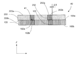
도 2(a)에 나타내는 바와 같이, 제1층의 반도체 칩(20)의 표면(20a)(도 1에 있어서 Z방향 플러스측의 면)의 우상측 모서리와 좌하측 모서리에는 각각 십자형의 얼라인먼트 마크(21a)가 설치되어 있다. 또, 제1층의 반도체 칩(20)에는 복수의 제1 관통 전극(22)이 설치되어 있다. 도 2(b)에 나타내는 바와 같이, 제1 관통 전극(22)은 제1층의 반도체 칩(20)의 표면(20a)과 이면(20b) 사이를 표면(20a), 이면(20b)에 대하여 수직으로 관통하도록 설치되어 있고, 제1층의 반도체 칩(20)의 표면(20a)에는 제1 관통 전극(22)의 표면(22a)이 노출되고, 제1층의 반도체 칩(20)의 이면(20b)에는 제1 관통 전극(22)의 표면(22a)과 동일 위치에 제1 관통 전극(22)의 이면(22b)이 노출되어 있다.As shown in Fig. 2 (a), an upper right corner and a lower left corner of a
제2층의 반도체 칩(30)도 제1층의 반도체 칩(20)과 마찬가지의 위치에 제2 관통 전극(32)이 설치되어 있다. 즉, 제2 관통 전극(32)은 제2층의 반도체 칩(30)을 반전시켜 그 이면(30b)을 제1층의 반도체 칩(20)의 표면(20a)에 겹쳤을 때에 동일한 위치가 되는 위치에 설치되어 있다. 그리고 제1층의 반도체 칩(20)과 마찬가지로 도 2(d)에 나타내는 바와 같이, 제2 관통 전극(32)은 제2층의 반도체 칩(30)의 표면(30a)과 이면(30b) 사이를 표면(30a), 이면(30b)에 대하여 수직으로 관통하도록 설치되어 있고, 제2층의 반도체 칩(30)의 표면(30a)에는 제2 관통 전극(32)의 표면(32a)이 노출되고, 제2층의 반도체 칩(30)의 이면(30b)에는 제2 관통 전극(32)의 표면(22a)과 동일 위치에 제2 관통 전극(32)의 이면(32b)이 노출되어 있다. 도 2(c)는 제2층의 반도체 칩(30)을 이면(30b)의 측에서 본 도면이며, 제2층의 반도체 칩(30)의 이면(30b)의 좌상측 모서리와 우하측 모서리(제2층의 반도체 칩(30)을 반전시켜 이면(30b)을 제1층의 반도체 칩(20)의 표면(20a)에 겹쳤을 때에 동일한 위치가 되는 위치)에는 각각 십자형의 얼라인먼트 마크(31b)가 설치되어 있다.The second-
도 1에 나타내는 바와 같이, 적층 본딩 전의 초기 상태에서는, 본딩 툴(14)은 상방의 대기 위치에 있으므로, 제어부(50)는 도시하지 않는 2시야 카메라 구동 기구에 의해 2시야 카메라(16)를 본딩 툴(14)과 본딩 스테이지(11)의 중간에 삽입한다. 그러면 도 1의 하방향의 안을 비운 화살표로 나타내는 2시야 카메라(16)의 하측의 시야에는 도 2(a)에 나타내는 바와 같이 얼라인먼트 마크(21a)와 제1 관통 전극(22)의 표면(22a)을 포함하는 제1층의 반도체 칩(20)의 표면(20a)의 화상이 포착되고, 도 1의 상방향의 안을 비운 화살표로 나타내는 2시야 카메라(16)의 상측의 시야에는 도 2(c)에 나타내는 바와 같이 얼라인먼트 마크(31b)와 제2 관통 전극(32)의 이면(32b)을 포함하는 제2층의 반도체 칩(30)의 이면(30b)의 화상이 포착된다.As shown in Fig. 1, in the initial state before laminate bonding, the
제어부(50)는 도 1에 나타내는 제1 촬상 프로그램(54)을 실행하고, 도 3의 스텝(S101)에 나타내는 바와 같이 2시야 카메라(16)를 작동시켜 도 2(a)에 나타내는 제1층의 반도체 칩(20)의 표면(20a)의 제1 관통 전극(22)의 표면(22a)의 화상을 촬상하여 메모리(52)의 제어 데이터(63)에 격납한다(제1 촬상 공정).The
또, 제어부(50)는 도 1에 나타내는 제1 본딩 프로그램(55)을 실행한다. 제어부(50)는 도 3의 스텝(S102)에 나타내는 바와 같이, 2시야 카메라(16)를 작동시켜 도 2(a)에 나타내는 제1층의 반도체 칩(20)의 표면(20a)의 얼라인먼트 마크(21a)를 촬상하여 메모리(52)의 제어 데이터(63)에 격납하고, 도 3의 스(S103)에 나타내는 바와 같이, 2시야 카메라(16)를 작동시켜 도 2(c)에 나타내는 제2층의 반도체 칩(30)의 이면(30b)의 얼라인먼트 마크(31b)를 촬상하여, 메모리(52)의 제어 데이터(63)에 격납한다. 제어부(50)는 각 얼라인먼트 마크(21a, 31b)의 화상을 처리하고, 각 얼라인먼트 마크(21a, 31b)의 위치의 XY 방향 또는 θ방향의 어긋남량을 검출하여, 본딩 스테이지 구동 기구(13), 본딩 툴 구동 기구(15)에 의해 각각 본딩 스테이지(11)의 XY 방향의 위치, 본딩 툴(14)의 θ방향의 위치를 조정한다. 그리고 각 얼라인먼트 마크(21a, 31b)의 위치의 XY 방향 또는 θ방향의 어긋남량이 각각 제로 또는 소정의 역치 이하가 되면, 제어부(50)는 제1층의 반도체 칩(20)과 제2층의 반도체 칩(30)의 각 얼라인먼트 마크(21a, 31b)의 위치가 맞았다고 판단하고, 도 3의 스텝(S104)에 나타내는 바와 같이, 본딩 툴 구동 기구(15)에 의해 본딩 툴(14)을 강하시키는 지령을 출력한다. 이 지령에 의해 도 4에 나타내는 바와 같이 본딩 툴(14)이 강하하고, 도 5(a)에 나타내는 바와 같이 제1층의 반도체 칩(20) 위에 제2층의 반도체 칩(30)을 적층 본딩하여, 다층 반도체 장치(40)로 한다(제1 본딩 공정).In addition, the
도 5(b)에 나타내는 바와 같이 제1층의 반도체 칩(20) 위에 제2층의 반도체 칩(30)을 적층 본딩하면, 제1층의 관통 전극(22)의 표면(22a)과, 제2층의 관통 전극(32)의 이면(32b) 사이에는 용융한 땜납이 굳은 고착층(41)이 형성되고, 이 고착층(41)에 의해 각 관통 전극(22, 32)이 접속되어 있다.5 (b), when the
도 6에 나타내는 바와 같이, 제1 본딩 공정이 종료되면, 제어부(50)는 본딩 툴(14)을 대기 위치까지 상승시키고, 도시하지 않는 2시야 카메라 구동 기구에 의해 2시야 카메라(16)를 제2층의 반도체 장치 칩(30) 위로 이동시킨다. 2시야 카메라(16)의 시야에는 도 5(a)에 나타내는 바와 같이 제1층의 반도체 칩(20) 위에 제2층의 반도체 칩(30)이 적층된 상태의 화상이 포착된다. 도 5(a)에서는 하측의 제1층의 반도체 칩(20)의 얼라인먼트 마크(21a), 제1 관통 전극의 표면(22a)은 파선으로 나타내는데, 실제로 2시야 카메라(16)의 시야에 비추어지는 것은 도 5(a)에 나타내는 실선의 부분, 즉 제2층의 반도체 칩(30)의 표면(30a) 및 제2 관통 전극(32)의 표면(32a)이다.6, when the first bonding process is completed, the
제어부(50)는 도 1에 나타내는 제2 촬상 프로그램(56)을 실행시켜, 도 3의 스텝(S105)에 나타내는 바와 같이, 제2층의 반도체 칩(30)의 표면(30a)의 제2 관통 전극(32)의 표면(32a)의 화상을 촬상하여, 제어 데이터(63)에 격납한다(제2 촬상 공정).The
제어부(50)는 도 1에 나타내는 상대 위치 검출 프로그램(53)을 실행하고, 도 3에 나타내는 스텝(S106)에 나타내는 바와 같이, 우선 제1 촬상 공정에서 촬상한 제1층의 반도체 칩(20)의 관통 전극(22)의 표면(22a)의 화상에 제2 촬상 공정에서 촬상한 제2층의 반도체 칩(30)의 관통 전극(32a)의 화상을 겹친다. 도 5(a)에서는 겹친 제1층의 반도체 칩(20)의 표면(20a), 제1 관통 전극(22)의 표면(22a)은 파선으로 나타내고 있다. 겹친 화상에는 각 관통 전극의 표면(22a, 32a)의 위치가 어긋나게 표시된다.The
앞서 설명한 바와 같이, 각 관통 전극(22, 32)은 각 층의 반도체 칩(20, 30)의 각 표면(20a, 30a)에 대하여 수직으로 형성되어 있는 점에서, 각 관통 전극의 표면(22a, 32a)의 위치가 어긋나 있다고 하는 것은, 도 5(b)에 나타내는 바와 같이 각 층의 반도체 칩(20, 30)이 어긋나서 적층되어 있다고 판단된다.Since the penetrating
또, 각 층의 반도체 칩(20, 30)의 각 얼라인먼트 마크(21a, 31b)의 위치를 맞추어 적층 본딩하고 있는 점에서, 각 층의 반도체 칩(20, 30)의 상대 위치는 크게 어긋나 있지 않고, 복수의 각 관통 전극(22, 32)의 위치는 서로 대응하는 위치에 있는 전극이 서로 겹쳐져 있는 상태로 되어 있다. 그래서, 제어부(50)는 도 5(a)에 나타내는 바와 같이 서로 겹쳐져 있는 제1 관통 전극(22)과의 표면(22a)과 제2 관통 전극(32)의 표면(32a)의 XY 방향의 어긋남량(ΔX, ΔY)을 제1층의 반도체 칩(20)과 제2층의 반도체 칩(30)의 상대 위치라고 판단한다. 도 5(a)에 나타내는 예에서는 제1층의 반도체 칩(20)의 표면(20a)에 설치된 얼라인먼트 마크(21a)와 제2층의 반도체 칩(30)의 이면(30b)에 설치된 얼라인먼트 마크(31b)의 위치도 어긋나 있으므로, 각 어긋남량(ΔX, ΔY)은 예를 들면 제어부(50)가 얼라인먼트 마크(21a, 31b)의 화상으로부터 얼라인먼트 마크의 위치를 인식할 때의 오차에 의해 생기는 각 관통 전극(22, 32)의 XY 방향의 위치 어긋남, 또는 적층 본딩시에 관통 전극 사이에 끼어 있는 용융 땜납에 의해 생긴 위치의 어긋남이라고 판단된다. 그리고, 제어부(50)는 도 3의 스텝(S107)에 나타내는 바와 같이, 도 3에 나타내는 스텝(S101~S106)의 각 스텝을 소정의 회수, 예를 들면 n회 반복한 후, 도 3의 스텝(S108)에 나타내는 바와 같이, 예를 들면 그 평균 어긋남량 또는 중앙값 등을 오프셋량으로서 설정한다(오프셋량 설정 공정).In addition, since the alignment marks 21a and 31b of the semiconductor chips 20 and 30 of the respective layers are aligned and laminated, the relative positions of the semiconductor chips 20 and 30 of the respective layers are not greatly shifted , The positions of the plurality of through
상기한 실시형태에서는 도 5(a)에 나타내는 제1 관통 전극(22)과의 표면(22a)과 제2 관통 전극(32)의 표면(32a)의 XY 방향의 어긋남량(ΔX, ΔY)(X는 제1층의 반도체 칩(20)의 기준축이며 예를 들면 도 5(a)에 나타내는 제1층의 반도체 칩(20)의 횡방향의 변 X와 평행한 방향이며, Y는 X방향에 대하여 직교하는 방향)을 제1층의 반도체 칩(20)과 제2층의 반도체 칩(30)의 상대 위치라고 판단하는 것으로서 설명했지만, 복수의 각 관통 전극(22, 32)의 각 표면(22a, 32a)의 화상을 사용하여, XY 방향의 어긋남량(ΔX, ΔY)뿐만아니라 제1층의 반도체 칩(20)에 대한 제2층의 반도체 칩의 회전 방향의 위치 어긋남(Δθ)을 포함하여 상대 위치라고 판단하는 것으로 해도 된다. 회전 방향의 위치 어긋남(Δθ)은 예를 들면 도 5(a)에 나타내는 최상부의 좌측의 관통 전극(22, 32)의 각 표면(22a, 32a)의 XY 방향의 어긋남량(ΔX1, ΔY1)과, 도 5(a)에 나타내는 최하부 우측의 관통 전극(22, 32)(대각 방향에 있는 관통 전극(22, 32))의 각 표면(22a, 32a)의 XY 방향의 어긋남량(ΔX2, ΔY2)을 사용하여 기준이 되는 X축에 대한 회전 각도(Δθ)로서 구하도록 해도 된다. 이 경우, 각 어긋남량(ΔX, ΔY, Δθ)의 평균값 또는 중앙값을 XYθ 방향의 각 오프셋량으로서 설정한다.In the above-described embodiment, the displacement amount? X,? Y (in the XY direction) between the
이상 설명한 본 실시형태의 티칭 동작(도 3에 나타내는 스텝(S106~S108))은 적층 본딩한 제1, 제2층의 반도체 칩(20, 30)을 떼어 접합면을 확인하거나, 적층한 다층 반도체 장치(40)를 절단하고, 예를 들면 도 5(b)에 나타내는 바와 같은 단면을 노출시켜 제1, 제2 관통 전극(22, 32)의 위치를 확인하거나 하는 것 같은 파괴 검사를 행하지 않고, 적층 본딩시의 제1층과 제2층의 반도체 칩(20, 30)의 위치 어긋남량(상대 위치)을 검출하고, 그 어긋남량(상대 위치)에 기초하여 적층 본딩시의 오프셋량을 설정한다는 간편한 방법으로 플립칩 본딩 장치의 티칭을 행할 수 있고, 각 관통 전극(22, 32)을 정밀도 좋게 접합할 수 있다.The above-described teaching operation (steps S106 to S108 shown in Fig. 3) is performed by peeling the semiconductor chips 20 and 30 of the first and second layers laminated and bonded to each other to confirm the bonding surfaces, The
다음에, 티칭 후의 다층 반도체 장치(40)를 제조하는 경우의 적층 본딩 동작(도 3의 스텝(S109)~스텝(S119))에 대해서 설명한다. 앞서 설명한 티칭 동작과 마찬가지의 공정에 대해서는 설명을 생략한다.Next, the multilayer bonding operation (steps S109 to S119 in Fig. 3) in the case of manufacturing the
앞서 티칭의 동작에서 설명한 것과 마찬가지로, 제어부(50)는 우선 본딩 스테이지(11) 위에 제1층의 반도체 칩(20)을 흡착 고정시키고, 도시하지 않는 픽업 유닛에 의해 웨이퍼로부터 제2층의 반도체 칩(30)을 본딩 툴(14)의 선단에 흡착시키고, 2시야 카메라(16)를 본딩 스테이지(11)와 본딩 툴(14) 사이에 삽입한다. 그리고 제어부(50)는 도 1에 나타내는 제1 촬상 프로그램(54)을 실행하고, 도 3의 스텝(S109)에 나타내는 바와 같이 2시야 카메라(16)를 작동시켜 도 2(a)에 나타내는 제1층의 반도체 칩(20)의 표면(20a)의 제1 관통 전극(22)의 표면(22a)의 화상을 촬상하여 메모리(52)의 제어 데이터(63)에 격납한다(제1 촬상 공정).The
다음에 제어부(50)는 도 1에 나타내는 제2 본딩 프로그램(58)을 실행한다. 제어부(50)는 도 3의 스텝(S110)에 나타내는 바와 같이, 2시야 카메라(16)를 작동시켜 도 2(a)에 나타내는 제1층의 반도체 칩(20)의 표면(20a)의 얼라인먼트 마크(21a)를 촬상하여 메모리(52)의 제어 데이터(63)에 격납하고, 도 3의 스텝(S111)에 나타내는 바와 같이, 2시야 카메라(16)를 작동시켜 도 2(c)에 나타내는 제2층의 반도체 칩(30)의 이면(30b)의 얼라인먼트 마크(31b)를 촬상하여, 메모리(52)의 제어 데이터(63)에 격납한다. 제어부(50)는 각 얼라인먼트 마크(21a, 31b)의 화상을 처리하고, 각 얼라인먼트 마크(21a, 31b)의 위치의 XY 방향 또는 θ방향의 어긋남량을 검출한다. 그리고, 제어부(50)는 도 3의 스텝(S112)에 나타내는 바와 같이, 각 얼라인먼트 마크(21a, 31b)의 위치의 XY 방향 또는 θ방향의 어긋남량이 각각 도 3의 스텝(S108)에서 설정한 오프셋량이 되도록, 본딩 스테이지 구동 기구(13), 본딩 툴 구동 기구(15)에 의해 각각 본딩 스테이지(11)의 XY 방향의 위치, 본딩 툴(14)의 θ방향의 위치를 조정하여, 각 얼라인먼트 마크(21a, 31b)의 어긋남량이 오프셋량이 되면, 도 3의 스텝(S112)에 나타내는 바와 같이, 본딩 툴 구동 기구(15)에 의해 본딩 툴(14)을 강하시키는 지령을 출력한다. 이 지령에 의해 도 4에 나타내는 바와 같이 본딩 툴(14)이 강하하고, 도 7(a)에 나타내는 바와 같이 제1층의 반도체 칩(20) 위에 제2층의 반도체 칩(30)을 적층 본딩하여, 다층 반도체 장치(40)로 한다(제2 본딩 공정).Next, the
제2 본딩 공정이 종료하면, 제어부(50)는 도 6에 나타내는 바와 같이, 본딩 툴(14)을 대기 위치까지 상승시키고, 도시하지 않는 2시야 카메라 구동 기구에 의해 2시야 카메라(16)를 제2층의 반도체 칩(30) 위로 이동시키고, 도 1에 나타내는 제3 촬상 프로그램(59)을 실행시켜, 도 3의 스텝(S113)에 나타내는 바와 같이 제2층의 반도체 칩(30)의 표면(30a)의 제2 관통 전극(32)의 표면(32a)의 화상을 촬상하여, 제어 데이터(63)에 격납한다(제3 촬상 공정).When the second bonding process is completed, the
상기한 제2 본딩 동작에서는, 도 3의 스텝(S101~S108)에 나타낸 티칭 동작에 의해 설정된 오프셋량만큼 미리 제2층의 반도체 칩(30)을 제1층의 반도체 칩(20)에 대하여 옮기고 있으므로, 적층 본딩을 한 후에는 도 5(a), 도 5(b)에 나타낸 티칭 동작시에 나타난 어긋남량(ΔX, ΔY 또는 Δθ)은 제로가 되어 있고, 도 7(a), 도 7(b)에 나타내는 바와 같이, 각 관통 전극(22, 32)은 어긋남 없이 겹쳐져 있을 것이다. 그러나 각 층의 반도체 칩(20, 30)의 각 얼라인먼트 마크(21a, 31b)의 부정확함 또는 플립칩 본딩 장치(500)의 온도 변화, 또는 각 층의 반도체 칩(20, 30)의 관통 전극(22, 32)의 위치의 제조 오차 등에 의해, 티칭 동작(도 3의 스텝(S101~S108))에 의해 오프셋량을 설정해도, 제2 본딩 동작 후에 도 5(a), 도 5(b)에 나타낸 바와 같은 각 관통 전극(22, 32)의 위치 어긋남이 발생하는 일이 있다.In the second bonding operation, the
그래서, 제어부(50)는 제2 본딩 동작 후, 도 3의 스텝(S113)에 나타내는 바와 같이, 2시야 카메라(16)에 의해 적층 본딩 후의 제2층의 반도체 칩(30)의 제2 관통 전극(32)의 표면(32a)의 화상을 취득하고, 도 1에 나타내는 어긋남량 검출 프로그램(60)을 실행하여, 도 3의 스텝(S114)에 나타내는 바와 같이, 도 3의 스텝(S109)에서 촬상한 제1층의 반도체 칩(20)의 제1 관통 전극(22)의 표면(22a)의 화상에 겹쳐지게 함으로써, 제1 관통 전극(22)의 위치와 제2 관통 전극(32)의 어긋남량(ΔX, ΔY, Δθ)을 검출한다(어긋남량 검출 공정).Thus, after the second bonding operation, the
또한, 어긋남량 검출 프로그램(60)은 오프셋량만큼 제1층과 제2층의 반도체 칩(20, 30)을 옮긴 제2 본딩 후에 실행하는 점을 제외하면, 앞서 설명한 도 1에 나타내는 상대 위치 검출 프로그램(53)과 마찬가지이다.The misalignment
그리고, 도 3의 스텝(S115)에 나타내는 바와 같이, 검출한 어긋남량이 허용 어긋남량인 제1 역치 미만이며, 또한 보정 필요 어긋남량인 제2 역치 이상인 경우에는 오프셋량을 보정할 필요가 있다고 판단하고, 도 3의 스텝(S116)에 나타내는 바와 같이 도 1에 나타내는 오프셋량 보정 프로그램(61)을 실행한다. 오프셋량 보정 프로그램(61)은 도 3의 스텝(S114)에서 검출한 어긋남량의 소정의 비율, 예를 들면 50% 등 만큼 오프셋량을 증감하는 것이다. 그리고, 오프셋량의 보정이 종료되면, 제어부(50)는 도 3의 스텝(S117)에 나타내는 바와 같이, 다음 본딩을 행하기 위해서 스텝(S109)로 되돌아간다. 이것에 의해 각 관통 전극(22, 32)을 정밀도 좋게 접합할 수 있다(오프셋량 보정 공정).3, it is determined that it is necessary to correct the offset amount when the detected shift amount is less than the first threshold value, which is the permissible shift amount, and is equal to or larger than the second threshold value, which is the correction required shift amount , And executes the offset
또한, 다음 본딩시에 도 3의 스텝(S109)에서 취득하는 제1층의 반도체 칩의 제1 관통 전극 표면의 화상은 그 전의 본딩시에 도 3의 스텝(S113)에서 취득한 제2층의 반도체 칩의 제2 관통 전극 표면의 화상이며, 이 화상은 메모리(52)에 격납되어 있다. 따라서 실제의 적층 본딩에서는 다음 본딩으로 이행하는 경우에 스텝(S109)를 생략하여 스텝(S110)으로 되돌아가도록 해도 된다.In the next bonding, the image of the surface of the first penetrating electrode of the first-layer semiconductor chip obtained in step S109 of Fig. 3 is transferred to the second-layer semiconductor obtained in step S113 in Fig. Is an image of the surface of the second penetrating electrode of the chip, and this image is stored in the
또, 도 3의 스텝(S118)에 나타내는 바와 같이, 제어부(50)는 검출한 어긋남량이 허용 어긋남량인 제1 역치를 넘고 있는 경우에는, 그 적층 본딩은 불량이라고 판단하여 도 1에 나타내는 정지 프로그램(62)을 실행하고, 도 3의 스텝(S119)에 나타내는 바와 같이, 플립칩 본딩 장치(500)를 정지시키고, 예를 들면 경고등을 점등시켜 이상 상태가 발생한 것을 알린다(정지 공정).As shown in step S118 in Fig. 3, when the detected displacement amount exceeds the first threshold value, which is the permissible shift amount, the
이상 설명한 본 실시형태의 본딩 장치에서는 적층하는 각 층의 반도체 칩(20, 30)의 파괴 검사를 행하지 않고 제조 중의 오프셋량의 보정, 불량 발생시의 본딩 장치의 정지를 행할 수 있으므로, 적층 본딩의 품질을 향상시킬 수 있다.As described above, in the bonding apparatus of the present embodiment, it is possible to correct the offset amount during manufacturing and to stop the bonding apparatus when defects occur, without performing destructive inspection of the semiconductor chips 20 and 30 of the respective layers to be laminated. Can be improved.
이상 설명한 실시형태에서는 2층에 반도체 칩을 적층 본딩하는 것에 대해서 설명했지만, 본 발명은 보다 다층의 적층 본딩에도 적용하는 것이 가능하다. 또, 오프셋량은 제1층과, 제2층의 본딩시의 오프셋량과 제2층과 제3층의 본딩시의 오프셋량을 변화시키도록 해도 된다. 또, 본 실시형태에서는 티칭 동작시에 제1층의 반도체 칩(20)의 얼라인먼트 마크(21a)와 제2층의 반도체 칩(30)의 얼라인먼트 마크(31b)의 위치를 맞추어 적층 본딩하는 것으로서 설명했지만, 각 얼라인먼트 마크(21a, 31b)가 겹쳐 있지 않아도, 각 얼라인먼트 마크간의 상대 거리를 알고 있는 경우에는 그 상대 거리만큼 얼라인먼트 마크를 옮겨 적층 본딩하는 것도, 얼라인먼트 마크를 맞추어 본딩하는 것에 포함된다.In the embodiment described above, the lamination bonding of semiconductor chips to two layers has been described. However, the present invention can be applied to multilayer bonding. The offset amount may be changed by varying the offset amount at the time of bonding the first layer and the second layer and the offset amount at the time of bonding the second layer and the third layer. In the present embodiment, it is described that the alignment marks 21a of the first-
또한, 본 실시형태의 플립칩 본딩 장치(500)에서는 본딩 스테이지(11)가 XY 방향으로 이동하고, 본딩 툴이 Z, θ 방향으로 이동하는 것으로서 설명했지만, 이 구성에 얽매이지 않고, 예를 들면 본딩 툴이 Y, Z, θ의 방향으로 이동하고, 본딩 스테이지(11)가 X방향만으로 이동하도록 구성해도 되고, 본딩 스테이지(11)가 이동하지 않고, 본딩 툴이 XYZ, θ방향으로 이동하도록 구성해도 된다.In the flip
다음에, 도 8 내지 도 11을 참조하면서, 도 1에 나타낸 플립칩 본딩 장치(500)를 사용하여 3층 이상으로 반도체 칩을 적층 본딩하는 공정((3층 이상으로 반도체 칩을 적층하는 반도체 장치의 제조 공정))에 대해서 설명한다. 도 1 내지 도 7을 참조하여 설명한 부분과 동일한 부분에는 동일한 부호를 붙이고 그 설명은 생략한다.Next, referring to Figs. 8 to 11, the flip
도 8의 스텝(S201) 내지 스텝(S208)의 티칭 동작에 대해서 설명한다. 이 티칭 동작은 도 3의 스텝(S101)~스텝(S108)의 동작과 마찬가지의 동작에 의해, 도 10에 나타내는 제1층(첫번째 층)의 반도체 칩(100)과, 첫번째 층에 인접하고 첫번째 층의 반도체 칩(100)의 상측에 적층 본딩되어 있는 제2층의 반도체 칩(200) 사이의 오프셋량을 결정하는 동작이다.The teaching operation of the steps S201 to S208 of Fig. 8 will be described. This teaching operation is performed by the same operation as the operations of steps S101 to S108 of Fig. 3, and the
제어부(50)는 도 8의 스텝(S201, S202)에 나타내는 바와 같이, 도 10에 나타내는 제1층(첫번째 층)의 반도체 칩(100)의 제1관통 전극(102)의 표면(102a)의 화상의 취득과, 제1층(첫번째 층)의 반도체 칩(100)의 표면(100a)의 얼라인먼트 마크의 화상을 취득한 후, 도 8의 스텝(S203)에 나타내는 바와 같이, 도 10에 나타내는 제2층의 반도체 칩(200)의 이면(200b)의 얼라인먼트 마크의 화상을 취득한다. 그리고 제어부(50)는 도 8의 스텝(S204)에 나타내는 바와 같이, 도 10에 나타내는 제1층(첫번째 층)의 반도체 칩(100) 위에 제2층의 반도체 칩(200)을 적층 본딩한다. 적층 본딩 후, 제어부(50)는 도 8의 스텝(S205)에 나타내는 바와 같이, 제2층의 반도체 칩(200)의 제2 관통 전극(202)의 표면(202a)의 화상을 취득하고, 도 8의 스텝(S201)에서 취득한 제1 관통 전극(102)의 표면(102a)의 화상과 도 8의 스텝(S205)에서 취득한 제2 관통 전극(202)의 표면(202a)의 화상에 기초하여, 도 8의 스텝(S206)에 나타내는 바와 같이 제1층의 반도체 칩(100)과 제2층의 반도체 칩(200) 사이의 X방향의 어긋남량(ΔX)을 검출한다. 그리고, 제어부(50)는 스텝(S201 내지 S206)과 같이 반도체 칩을 2층으로 적층한 경우의 첫번째 층(제1층)과 제2층의 각 반도체 칩(100, 200)의 어긋남량을 소정의 회수만큼 검출하고, 도 8의 스텝(S207)에 나타내는 바와 같이 소정의 회수 반복했다고 판단하면, 예를 들면 소정의 회수의 어긋남량(ΔX)의 평균값을 오프셋량으로서 설정한다. 또한, 오프셋량의 설정은 제어부(50)에 격납된 오프셋량 설정 프로그램(57)을 실행시키지 않고, 오퍼레이터가 수동으로 설정해도 된다.The
도 8의 스텝(S201~S208)에 나타내는 티칭 동작에 의해 적층 본딩시의 오프셋량을 설정하면, 제어부(50)는 도 9의 스텝(S209~S220)에 나타내는 바와 같이, 실제의 다층 반도체 장치(40)의 제조를 개시한다. 이 동작은 도 3의 스텝(S109)~스텝(S114)의 동작과 마찬가지의 동작에 의해, 도 11(b)에 나타내는 바와 같이, 적층한 반도체 칩(100~300)의 각 층간 어긋남량(ΔX12, ΔX23)을 검출함과 동시에 제1층의 반도체 칩(100)에 대한 제3층의 반도체 칩(300)의 적산 어긋남량(ΔX13)을 검출하고, 각 층간 어긋남량(ΔX12, ΔX23) 또는 적산 어긋남량(ΔX13)이 소정의 역치 이상이 된 경우에는 본딩을 정지하는 것이다.The
우선, 제어부(50)는 도 9의 스텝(S209)에 나타내는 바와 같이, 카운터(N)에 초기값 1을 세트한다. 다음에 제어부(50)는 도 9의 스텝(S210, 211)에 나타내는 바와 같이, 도 11(a)에 나타내는 제1층(N=1)의 반도체 칩(100)의 제1 관통 전극(N=1)(102)의 표면(102a)의 화상의 취득과, 제1층(N=1)의 반도체 칩(100) 표면(100a)의 얼라인먼트 마크의 화상을 취득한 후, 도 9의 스텝(S212)에 나타내는 바와 같이, 도 11(a)에 나타내는 제2층(N+1=2)의 반도체 칩(200)의 이면(200b)의 얼라인먼트 마크의 화상을 취득한다. 그리고 제어부(50)는 도 9의 스텝(S213)에 나타내는 바와 같이, 소정의 오프셋량만큼 각 얼라인먼트 마크의 위치를 옮겨 도 11(a)에 나타내는 제1층(N=1)의 반도체 칩(100) 위에 제2층(N+1=2)의 반도체 칩(200)을 적층 본딩한다.First, the
적층 본딩 후, 제어부(50)는 도 9의 스텝(S214)에 나타내는 바와 같이, 제2층(N+1=2)의 반도체 칩(200)의 제2 관통 전극(202)의 표면(202a)의 화상을 취득하고, 도 9의 스텝(S210)에서 취득한 제1 관통 전극(102)의 표면(102a)의 화상과 도 9의 스텝(S214)에서 취득한 제2 관통 전극(202)의 표면(202a)의 화상에 기초하여, 도 9의 스텝(S215)에 나타내는 바와 같이 제1층(N=1)의 반도체 칩(100)과 제2층(N+1=2)의 반도체 칩(200) 사이의 X방향의 층간 어긋남량(ΔX12)을 검출한다. 오프셋량과 적층 본딩시의 어긋남량이 동일한 경우에는 제1층과 제2층의 반도체 칩간의 상대 위치는 동일하며 층간 어긋남량(ΔX12)은 제로가 되지만, 실제로는 오프셋량과 적층 본딩시의 어긋남량 사이에도 약간의 오차가 있다. 이 때문에 도 11(a)에 나타내는 바와 같이, 오프셋량만큼 제2층의 반도체 칩(200)을 옮겨 적층 본딩해도 제1층의 반도체 칩(100)과 제2층의 반도체 칩(200) 사이에는 약간의 층간 어긋남량(ΔX12)이 발생한다.After the laminate bonding, the
또, 제어부(50)는 도 9의 스텝(S216)에 나타내는 바와 같이, 도 9의 스텝(S210)에서 취득한 제1 관통 전극(102)의 표면(102a)의 화상과 도 9의 스텝(S214)에서 취득한 제2 관통 전극(202)의 표면(202a)의 화상에 기초하여, 제1층의 반도체 칩(100)과 제2층(N+1=2)의 반도체 칩(200) 사이의 X방향의 적산 어긋남량을 검출한다. 적층수가 2층인 경우, 이 적산 어긋남량은 앞선 층간 어긋남량(ΔX12)과 동일하게 된다.9, the
다음에 제어부(50)는 도 9의 스텝(S217)에 나타내는 바와 같이, 제1층과 제2층의 반도체 칩(100, 200) 사이의 층간 어긋남량(ΔX12)과 제3 역치를 비교하여, 층간 어긋남량(Δ12)이 제3 역치 이상이 된 경우에는 본딩 불량이라고 판단하고, 도 9의 스텝(S221)에 나타내는 바와 같이 본딩 동작을 정지한다. 또, 제어부(50)는 도 9의 스텝(S218)에 나타내는 바와 같이, 제1층과 제2층의 반도체 칩(100, 200) 사이의 적산 어긋남량과 제4의 역치를 비교하여, 적산 어긋남량이 제4 역치 이상이 된 경우에는 본딩 불량이라고 판단하고, 도 9의 스텝(S221)에 나타내는 바와 같이 본딩 동작을 정지한다. 앞서 설명한 바와 같이, 적층수가 2층인 경우에는 적산 어긋남량은 층간 어긋남량(ΔX12)과 동일하다.Next, as shown in step S217 of FIG. 9, the
그리고 제어부(50)는 층간 어긋남량, 적산 어긋남량 모두 제3, 제4 역치 미만인 경우에는, 도 9의 스텝(S219)에 나타내는 바와 같이, 소정의 층수만큼 반도체 칩을 본딩했는지 여부를 판단하고, 소정의 층수만큼 적층 본딩한 경우에는 제어부(50)는 도 9의 스텝(S221)에 나타내는 바와 같이 본딩을 정지한다. 또, 소정의 층수만큼 적층 본딩하고 있지 않다고 판단한 경우에는 도 9의 스텝(S220)에 나타내는 바와 같이 카운터(N)를 1만큼 인크리먼트하여 N=2로 하고, 도 9의 스텝(S211)로 되돌아가 제2층의 반도체 칩(200) 위에 도 11(b)에 나타내는 바와 같이 제3층의 반도체 칩(300)을 적층 본딩한다.9, the
제어부(50)는 도 9의 스텝(S211)에 나타내는 바와 같이, 도 11(b)에 나타내는 제2층(N=2)의 반도체 칩(200)의 표면(200a)의 얼라인먼트 마크의 화상을 취득한 후, 도 9의 스텝(S212)에 나타내는 바와 같이 도 11(b)에 나타내는 제3층(N+1=3)의 반도체 칩(300)의 이면(300b)의 얼라인먼트 마크의 화상을 취득한다. 그리고 제어부(50)는 도 9의 스텝(S213)에 나타내는 바와 같이, 소정의 오프셋량만큼 각 얼라인먼트 마크의 위치를 옮겨 도 11(b)에 나타내는 제2층(N=2)의 반도체 칩(200) 위에 제3층(N+1=3)의 반도체 칩(300)을 적층 본딩한다.The
적층 본딩 후, 제어부(50)는 도 9의 스텝(S214)에 나타내는 바와 같이, 제3층(N+1=3)의 반도체 칩(300)의 제3 관통 전극(302)의 표면(302a)의 화상을 취득하고, 전회의 루프(N=1)시의 도 9의 스텝(S214)에서 취득한 제2 관통 전극(202)의 표면(202a)의 화상과 금회의 루프(N=2)시의 도 9의 스텝(S214)에서 취득한 제3 관통 전극(302)의 표면(302a)의 화상에 기초하여, 도 9의 스텝(S215)에 나타내는 바와 같이, 제2층(N=2)의 반도체 칩(200)과 제3층(N+1=3)의 반도체 칩(300) 사이의 X방향의 층간 어긋남량(ΔX23)을 검출한다. 제1층과 제2층과 층간의 경우와 마찬가지로 오프셋량과 적층 본딩시의 어긋남량 사이에 약간의 오차가 있으므로 도 11(b)에 나타내는 바와 같이, 오프셋량만큼 제3층의 반도체 칩(300)을 옮겨 적층 본딩해도 제2층의 반도체 칩(200)과 제3층의 반도체 칩(300) 사이에는 약간의 층간 어긋남량(ΔX23)이 발생한다.After the laminate bonding, as shown in step S214 of FIG. 9, the
또, 제어부(50)는 도 9의 스텝(S216)에 나타내는 바와 같이, 도 9의 스텝(S210)에서 취득한 제1 관통 전극(102)의 표면(102a)의 화상과 금회의 루프(N=2)의 도 9의 스텝(S214)에서 취득한 제3 관통 전극(302)의 표면(302a)의 화상에 기초하여, 도 11(b)에 나타내는 바와 같이, 제1층의 반도체 칩(100)과 제3층(N+1=3)의 반도체 칩(300) 사이의 X방향의 적산 어긋남량(ΔX13)을 검출한다. 적산 어긋남량(ΔX13)은 제1층과 제2층의 각 반도체 칩(100, 200) 사이의 층간 어긋남량(ΔX12)에 제2층과 제3층의 각 반도체 칩(200, 300) 사이의 층간 어긋남량(ΔX23)을 더한 것이다(ΔX13=ΔX12+ΔX23). 도 11(b)에 나타내는 바와 같이, 제1층에 대한 제2층의 어긋남의 방향을 마이너스 방향(도면 중 좌방향)으로 하면, 제2층에 대한 제3층의 어긋남의 방향은 플러스 방향(도면 중 우방향)이 되므로, 제1층에 대한 제3층의 적산 어긋남량(ΔX13=ΔX12+ΔX23)의 절대값은 제1층과 제2층 사이의 층간 어긋남량(ΔX12)의 절대값보다 작게 되어 있다. 또, 반대로 제2층에 대한 제3층의 어긋남의 방향도 마이너스 방향(도면 중 좌방향)인 경우에는, 제1층에 대한 제3층의 적산 어긋남량(ΔX13=ΔX12+ΔX23)의 절대값은 제1층과 제2층 사이의 층간 어긋남량(ΔX12)의 절대값보다 크게 된다.9, the
다음에 제어부(50)는 도 9의 스텝(S217)에 나타내는 바와 같이, 제2층과 제3층의 반도체 칩(200, 300) 사이의 층간 어긋남량(ΔX23)과 제3 역치를 비교하여, 층간 어긋남량(Δ23)이 제3 역치 이상이 된 경우에는 본딩 불량이라고 판단하고, 도 9의 스텝(S221)에 나타내는 바와 같이 본딩 동작을 정지한다. 또, 제어부(50)는 도 9의 스텝(S218)에 나타내는 바와 같이, 제1층과 제3층의 반도체 칩(100, 300) 사이의 적산 어긋남량(ΔX13)과 제4 역치를 비교하여, 적산 어긋남량(ΔX13)이 제4 역치 이상이 된 경우에는 본딩 불량이라고 판단하고, 도 9의 스텝(S221)에 나타내는 바와 같이 본딩 동작을 정지한다.Next, as shown in step S217 of FIG. 9, the
그리고 제어부(50)는 층간 어긋남량(ΔX23), 적산 어긋남량(ΔX13) 모두 제3, 제4 역치 미만인 경우에는, 도 9의 스텝(S219)에 나타내는 바와 같이, 소정의 층수만큼 반도체 칩을 본딩했는지 여부를 판단하고, 소정의 층수만큼 적층 본딩한 경우에는 제어부(50)는 도 9의 스텝(S221)에 나타내는 바와 같이 본딩을 정지한다. 또, 소정의 층수만큼 적층 본딩하고 있지 않다고 판단한 경우에는 도 9의 스텝(S220)에 나타내는 바와 같이, 카운터(N)를 1만큼 인크리먼트하여 N=3으로 하고, 도 9의 스텝(S211)로 되돌아가 제3층의 반도체 칩(300) 위에 제4층의 반도체 칩을 적층 본딩한다.If the interlayer shift amount DELTA X23 and the cumulative shift amount DELTA X13 are both less than the third and fourth threshold values as shown in step S219 of Fig. 9, the
이상 설명한 실시형태에서는 층간 어긋남량(ΔX12, ΔX23)과, 적산 어긋남량(ΔX13)의 양쪽이 소정의 역치 이상이 된 경우에는 본딩을 정지하므로, 적층 본딩에 의해 제조하는 다층 반도체 장치(40)의 품질을 향상시킬 수 있다.In the above-described embodiment, when both the interlayer shift amounts DELTA X12 and DELTA X23 and the cumulative shift amount DELTA X13 are both equal to or more than a predetermined threshold value, the bonding is stopped. Therefore, in the
또한, 본 실시형태에서는 어긋남량은 X방향의 어긋남량(ΔX12, ΔX23, ΔX13)으로서 설명했지만, Y방향, θ방향의 어긋남량에 대해서도 마찬가지로 층간 어긋남량, 적산 어긋남량의 양쪽의 어긋남량이 소정의 역치 이상이 된 경우에 본딩을 정지하도록 해도 된다.In the present embodiment, the amount of displacement is described as X shift amount (X12, X23, X13) in the X direction, but also with respect to the Y shift amount in the Y direction and the X direction, The bonding may be stopped when the threshold value is exceeded.
본 발명은 이상 설명한 실시형태에 한정되는 것은 아니며, 청구의 범위에 의해 규정되어 있는 본 발명의 기술적 범위 내지 본질로부터 일탈하지 않는 모든 변경 및 수정을 포함하는 것이다.The present invention is not limited to the embodiments described above, but includes all changes and modifications which do not depart from the technical scope and nature of the present invention defined by the claims.
11…본딩 스테이지
12…XY 테이블
13…본딩 스테이지 구동 기구
14…본딩 툴
15…본딩 툴 구동 기구
16…2시야 카메라
20…제1층의 반도체 칩
20a, 22a, 30a, 32a…표면
20b, 22b, 30b, 32b…이면
21a, 31a, 31b…얼라인먼트 마크
22…제1 관통 전극
30…제2층의 반도체 칩
32…제2 관통 전극
40…다층 반도체 장치
41…고착층
50…제어부
51…CPU
52…메모리
53…상대 위치 검출 프로그램
54…제1 촬상 프로그램
55…제1 본딩 프로그램
56…제2 촬상 프로그램
57…오프셋량 설정 프로그램
58…제2 본딩 프로그램
59…제3 촬상 프로그램
60…어긋남량 검출 프로그램
61…오프셋량 보정 프로그램
62…정지 프로그램
63…제어 데이터
64…본딩 툴 구동 기구 인터페이스
65…2시야 카메라 인터페이스
66…본딩 스테이지 구동 기구 인터페이스
70…데이터 버스
100, 200, 300…반도체 칩
100a, 102a, 200a, 202a, 300a, 302a…표면
102, 202, 302…관통 전극
100b, 200b, 300b…이면
500…플립칩 본딩 장치11 ... Bonding stage
12 ... XY table
13 ... The bonding stage driving mechanism
14 ... Bonding tool
15 ... The bonding tool driving mechanism
16 ... 2-view camera
20 ... The semiconductor chip of the first layer
20a, 22a, 30a, 32a ... surface
20b, 22b, 30b, 32b ... If
21a, 31a, 31b ... Alignment mark
22 ... The first through-
30 ... The semiconductor chip of the second layer
32 ... The second through-
40 ... Multilayer semiconductor device
41 ... Fixing layer
50 ... The control unit
51 ... CPU
52 ... Memory
53 ... Relative position detection program
54 ... The first imaging program
55 ... The first bonding program
56 ... The second imaging program
57 ... Offset amount setting program
58 ... The second bonding program
59 ... The third imaging program
60 ... The shift amount detection program
61 ... Offset amount correction program
62 ... Stop program
63 ... Control data
64 ... Bonding tool drive mechanism interface
65 ... 2-view camera interface
66 ... Bonding stage drive mechanism interface
70 ... Data bus
100, 200, 300 ... Semiconductor chip
100a, 102a, 200a, 202a, 300a, 302a ... surface
102, 202, 302 ... Penetrating electrode
100b, 200b, 300b ... If
500 ... Flip chip bonding device
Claims (15)
반도체 칩의 화상을 촬상하는 카메라와,
상기 카메라가 촬상한 화상의 화상 처리와 제1 관통 전극이 설치되는 제1층의 상기 반도체 칩 위에 상기 제1 관통 전극에 대응하는 위치에 제2 관통 전극이 설치되는 제2층의 상기 반도체 칩을 적층 본딩하는 본딩 제어를 행하는 제어부를 포함하고,
상기 제어부는,
적층 본딩하기 전에 상기 카메라에 의해 촬상한 제1층의 반도체 칩 표면의 상기 제1 관통 전극의 화상과, 적층 본딩한 후에 상기 카메라에 의해 촬상한 제2층의 반도체 칩 표면의 상기 제2 관통 전극의 화상에 기초하여 적층 본딩된 상기 각 층의 반도체 칩의 상대 위치를 검출하는 상대 위치 검출 수단을 포함하는 것을 특징으로 하는 본딩 장치.As a bonding apparatus,
A camera for picking up an image of the semiconductor chip,
The image processing of the image picked up by the camera and the semiconductor chip of the second layer in which the second penetrating electrode is provided on the semiconductor chip of the first layer provided with the first penetrating electrode at a position corresponding to the first penetrating electrode, And a control section for performing bonding control for performing laminated bonding,
Wherein,
And an image of the first penetrating electrode on the surface of the semiconductor chip of the first layer taken by the camera before lamination bonding is formed on the surface of the semiconductor chip of the second layer picked up by the camera after lamination bonding, And relative position detecting means for detecting a relative position of the semiconductor chips of the respective layers laminated and bonded based on the image of the semiconductor chip.
상기 상대 위치는 상기 제1층의 반도체 칩 표면 상의 기준축을 따른 방향 또는 상기 기준축과 직교하는 방향의 상기 제2층의 반도체 칩의 위치 어긋남, 또는 상기 기준축에 대한 상기 제2층의 반도체 칩의 회전 각도의 어느 하나 또는 복수의 조합인 것을 특징으로 하는 본딩 장치.The method according to claim 1,
Wherein the relative position is a positional deviation of the semiconductor chip of the second layer in a direction along a reference axis on the surface of the semiconductor chip of the first layer or a direction orthogonal to the reference axis, And the angle of rotation of the bonding member.
상기 제1층의 반도체 칩과 상기 제2층의 반도체 칩은 인접하는 2개의 층의 각 반도체 칩인 것을 특징으로 하는 본딩 장치.The method according to claim 1,
Wherein the semiconductor chip of the first layer and the semiconductor chip of the second layer are semiconductor chips of two adjacent layers.
상기 제1층의 반도체 칩과 상기 제2층의 반도체 칩은 인접하는 2개의 층의 각 반도체 칩인 것을 특징으로 하는 본딩 장치.3. The method of claim 2,
Wherein the semiconductor chip of the first layer and the semiconductor chip of the second layer are semiconductor chips of two adjacent layers.
상기 제1층의 반도체 칩은 첫번째 층의 반도체 칩이며, 상기 제2층의 반도체 칩은 상기 첫번째 층의 반도체 칩의 상측에 적층 본딩된 다른 반도체 칩인 것을 특징으로 하는 본딩 장치.The method according to claim 1,
Wherein the semiconductor chip of the first layer is a semiconductor chip of the first layer and the semiconductor chip of the second layer is another semiconductor chip laminated and bonded to the upper side of the semiconductor chip of the first layer.
상기 제1층의 반도체 칩은 첫번째 층의 반도체 칩이며, 상기 제2층의 반도체 칩은 상기 첫번째 층의 반도체 칩의 상측에 적층 본딩된 다른 반도체 칩인 것을 특징으로 하는 본딩 장치.3. The method of claim 2,
Wherein the semiconductor chip of the first layer is a semiconductor chip of the first layer and the semiconductor chip of the second layer is another semiconductor chip laminated and bonded to the upper side of the semiconductor chip of the first layer.
상기 제어부는,
적층 본딩하기 전에 상기 카메라에 의해 제1층의 반도체 칩 표면의 상기 제1 관통 전극의 화상을 촬상하는 제1 촬상 수단과,
적층 본딩하기 전에 상기 카메라에 의해 촬상한 제1층의 반도체 칩 표면의 제1 얼라인먼트 마크와 적층 본딩하기 전에 상기 카메라에 의해 촬상한 제2층의 반도체 칩 이면의 제2 얼라인먼트 마크의 위치를 맞추어 상기 제2층의 반도체 칩을 상기 제1층의 반도체 칩 위에 적층 본딩하는 제1 본딩 수단과,
상기 제1 본딩 수단에 의해 적층 본딩한 후에 상기 카메라에 의해 제2층의 반도체 칩 표면의 상기 제2 관통 전극의 화상을 촬상하는 제2 촬상 수단과,
상기 제1 촬상 수단에 의해 촬상한 상기 제1 관통 전극의 화상과 상기 제2 촬상 수단에 의해 촬상한 상기 제2 관통 전극의 화상에 기초하여 상기 각 층의 반도체 칩의 상대 위치를 검출하고, 검출한 상대 위치를 적층 본딩시의 오프셋량으로서 설정하는 오프셋량 설정 수단
을 포함하는 것을 특징으로 하는 본딩 장치.The method according to claim 1,
Wherein,
First imaging means for imaging the image of the first penetrating electrode on the surface of the semiconductor chip of the first layer by the camera before laminate bonding,
Aligning the position of the second alignment mark on the back surface of the semiconductor chip of the second layer taken by the camera before the lamination bonding with the first alignment mark on the surface of the semiconductor chip of the first layer taken by the camera before the lamination bonding, First bonding means for layer-bonding the semiconductor chip of the second layer on the semiconductor chip of the first layer,
Second image pickup means for picking up an image of the second penetrating electrode on the surface of the semiconductor chip of the second layer by the camera after lamination bonding by the first bonding means,
The relative positions of the semiconductor chips of the respective layers are detected based on the images of the first penetrating electrodes picked up by the first picking-up means and the images of the second penetrating electrodes picked up by the second picking-up means, An offset amount setting means for setting a relative position as an offset amount at the time of laminate bonding
Wherein the bonding apparatus comprises:
상기 제어부는,
상기 제1 얼라인먼트 마크에 상기 제2 얼라인먼트 마크가 맞는 위치로부터 상기 오프셋량 설정 수단으로 설정한 오프셋량만큼 상기 제2층의 반도체 칩을 옮겨 상기 제1층의 반도체 칩 위에 적층 본딩하는 제2 본딩 수단과,
상기 제2 본딩 수단에 의해 적층 본딩한 후에 상기 카메라에 의해 제2층의 반도체 칩 표면의 상기 제2 관통 전극의 화상을 촬상하는 제3 촬상 수단과,
상기 제1 촬상 수단에 의해 촬상한 상기 제1 관통 전극의 화상과 상기 제3 촬상 수단에 의해 촬상한 상기 제2 관통 전극의 화상에 기초하여 상기 각 층의 반도체 칩의 상대 위치의 어긋남량을 검출하는 어긋남량 검출 수단
을 포함하는 것을 특징으로 하는 본딩 장치.8. The method of claim 7,
Wherein,
A second bonding means for transferring the semiconductor chip of the second layer by an offset amount set by the offset amount setting means from a position where the second alignment mark fits into the first alignment mark and laminating and bonding the semiconductor chip on the semiconductor chip of the first layer, and,
Third imaging means for picking up an image of the second penetrating electrode on the surface of the semiconductor chip of the second layer by the camera after lamination bonding by the second bonding means,
Based on the image of the first penetrating electrode picked up by the first picking-up means and the image of the second penetrating electrode picked up by the third picking-up means, the displacement amount of the relative position of the semiconductor chips of each layer is detected The shift amount detecting means
Wherein the bonding apparatus comprises:
상기 제어부는,
상기 어긋남량 검출 수단으로 검출한 어긋남량이 제1 역치 미만이며, 제2 역치 이상인 경우에는, 상기 어긋남량의 소정 비율만큼 상기 오프셋량을 보정하는 오프셋량 보정 수단을 포함하는 것을 특징으로 하는 본딩 장치.9. The method of claim 8,
Wherein,
And offset amount correcting means for correcting the offset amount by a predetermined ratio of the shift amount when the shift amount detected by the shift amount detecting means is less than the first threshold value and is equal to or larger than the second threshold value.
제1 관통 전극이 설치되는 제1층의 반도체 칩 위에 상기 제1 관통 전극에 대응하는 위치에 제2 관통 전극이 설치되는 제2층의 반도체 칩을 적층 본딩하는 본딩 장치를 준비하는 공정과,
적층 본딩하기 전에 카메라에 의해 제1층의 반도체 칩 표면의 상기 제1 관통 전극의 화상을 촬상하는 제1 촬상 공정과,
적층 본딩하기 전에 상기 카메라에 의해 촬상한 제1층의 반도체 칩 표면의 제1 얼라인먼트 마크와 적층 본딩하기 전에 상기 카메라에 의해 촬상한 제2층의 반도체 칩 이면의 제2 얼라인먼트 마크의 위치를 맞추어 상기 제2층의 반도체 칩을 상기 제1층의 반도체 칩 위에 적층 본딩하는 제1 본딩 공정과,
상기 제1 본딩 공정 후에 상기 카메라에 의해 제2층의 반도체 칩 표면의 상기 제2 관통 전극의 화상을 촬상하는 제2 촬상 공정과,
상기 제1 관통 전극의 화상과 상기 제2 관통 전극의 화상에 기초하여 상기 각 층의 반도체 칩의 상대 위치를 검출하고, 검출한 상대 위치를 적층 본딩시의 오프셋량으로서 설정하는 오프셋량 설정 공정
을 포함하는 것을 특징으로 하는 반도체 장치의 제조 방법.A method of manufacturing a semiconductor device,
Preparing a bonding apparatus for layer-bonding semiconductor chips of a second layer in which a second penetrating electrode is provided at a position corresponding to the first penetrating electrode on a first-layer semiconductor chip on which a first penetrating electrode is provided;
A first imaging step of picking up an image of the first penetrating electrode on the surface of the semiconductor chip of the first layer by a camera before lamination bonding,
Aligning the position of the second alignment mark on the back surface of the semiconductor chip of the second layer taken by the camera before the lamination bonding with the first alignment mark on the surface of the semiconductor chip of the first layer taken by the camera before the lamination bonding, A first bonding step of stacking and bonding the semiconductor chip of the second layer on the semiconductor chip of the first layer;
A second imaging step of picking up an image of the second penetrating electrode on the surface of the semiconductor chip of the second layer by the camera after the first bonding step;
An offset amount setting step of detecting a relative position of the semiconductor chip of each layer based on the image of the first penetrating electrode and the image of the second penetrating electrode and setting the detected relative position as an offset amount at the time of laminate bonding
And forming a second insulating film on the semiconductor substrate.
상기 제1 얼라인먼트 마크에 상기 제2 얼라인먼트 마크가 맞는 위치로부터 상기 오프셋량만큼 상기 제2층의 반도체 칩을 옮겨 상기 제1층의 반도체 칩 위에 적층 본딩하는 제2 본딩 공정과,
상기 제2 본딩 공정 후에 상기 카메라에 의해 제2층의 반도체 칩 표면의 상기 제2 관통 전극의 화상을 촬상하는 제3 촬상 공정과,
상기 제1 촬상 수단에 의해 촬상한 상기 제1 관통 전극의 화상과 상기 제3 촬상 수단에 의해 촬상한 상기 제2 관통 전극의 화상에 기초하여 상기 각 층의 반도체 칩의 상대 위치의 어긋남량을 검출하는 어긋남량 검출 공정
을 포함하는 것을 특징으로 하는 반도체 장치의 제조 방법.11. The method of claim 10,
A second bonding step of transferring the semiconductor chip of the second layer from the position where the second alignment mark fits to the first alignment mark by the offset amount and stacking and bonding the semiconductor chip on the semiconductor chip of the first layer,
A third imaging step of picking up an image of the second penetrating electrode on the surface of the semiconductor chip of the second layer by the camera after the second bonding step,
Based on the image of the first penetrating electrode picked up by the first picking-up means and the image of the second penetrating electrode picked up by the third picking-up means, the displacement amount of the relative position of the semiconductor chips of each layer is detected A shift amount detecting step
And forming a second insulating film on the semiconductor substrate.
상기 제1층의 반도체 칩과 상기 제2층의 반도체 칩은 인접하는 2개의 층의 각 반도체 칩인 것을 특징으로 하는 반도체 장치의 제조 방법.11. The method of claim 10,
Wherein the semiconductor chip of the first layer and the semiconductor chip of the second layer are semiconductor chips of adjacent two layers.
상기 제1층의 반도체 칩과 상기 제2층의 반도체 칩은 인접하는 2개의 층의 각 반도체 칩인 것을 특징으로 하는 반도체 장치의 제조 방법.12. The method of claim 11,
Wherein the semiconductor chip of the first layer and the semiconductor chip of the second layer are semiconductor chips of adjacent two layers.
상기 제1층의 반도체 칩은 첫번째 층의 반도체 칩이며, 상기 제2층의 반도체 칩은 상기 첫번째 층의 반도체 칩의 상측에 적층 본딩된 다른 반도체 칩인 것을 특징으로 하는 반도체 장치의 제조 방법.11. The method of claim 10,
Wherein the semiconductor chip of the first layer is a semiconductor chip of the first layer and the semiconductor chip of the second layer is another semiconductor chip laminated and bonded on the semiconductor chip of the first layer.
상기 제1층의 반도체 칩은 첫번째 층의 반도체 칩이며, 상기 제2층의 반도체 칩은 상기 첫번째 층의 반도체 칩의 상측에 적층 본딩된 다른 반도체 칩인 것을 특징으로 하는 반도체 장치의 제조 방법.12. The method of claim 11,
Wherein the semiconductor chip of the first layer is a semiconductor chip of the first layer and the semiconductor chip of the second layer is another semiconductor chip laminated and bonded on the semiconductor chip of the first layer.
Applications Claiming Priority (5)
| Application Number | Priority Date | Filing Date | Title |
|---|---|---|---|
| JPJP-P-2012-131510 | 2012-06-11 | ||
| JP2012131510 | 2012-06-11 | ||
| JPJP-P-2013-061589 | 2013-03-25 | ||
| JP2013061589A JP5876000B2 (en) | 2012-06-11 | 2013-03-25 | Bonding apparatus and bonding method |
| PCT/JP2013/065575 WO2013187292A1 (en) | 2012-06-11 | 2013-06-05 | Bonding device and method for producing semiconductor device |
Publications (2)
| Publication Number | Publication Date |
|---|---|
| KR20140117543A true KR20140117543A (en) | 2014-10-07 |
| KR101630249B1 KR101630249B1 (en) | 2016-06-14 |
Family
ID=49758118
Family Applications (1)
| Application Number | Title | Priority Date | Filing Date |
|---|---|---|---|
| KR1020147022686A Active KR101630249B1 (en) | 2012-06-11 | 2013-06-05 | Bonding device and method for producing semiconductor device |
Country Status (7)
| Country | Link |
|---|---|
| US (1) | US9385104B2 (en) |
| JP (1) | JP5876000B2 (en) |
| KR (1) | KR101630249B1 (en) |
| CN (1) | CN104335337B (en) |
| SG (1) | SG11201408122RA (en) |
| TW (1) | TWI511215B (en) |
| WO (1) | WO2013187292A1 (en) |
Cited By (1)
| Publication number | Priority date | Publication date | Assignee | Title |
|---|---|---|---|---|
| KR20210064601A (en) * | 2019-11-26 | 2021-06-03 | 세메스 주식회사 | Die bonding method |
Families Citing this family (20)
| Publication number | Priority date | Publication date | Assignee | Title |
|---|---|---|---|---|
| JP6454283B2 (en) * | 2013-11-27 | 2019-01-16 | 東レエンジニアリング株式会社 | 3D mounting method and 3D mounting apparatus |
| TWI567859B (en) * | 2014-02-10 | 2017-01-21 | 新川股份有限公司 | Mounting device and offset correction method thereof |
| JP6363854B2 (en) * | 2014-03-11 | 2018-07-25 | キヤノン株式会社 | Forming method and article manufacturing method |
| JP6305887B2 (en) * | 2014-09-16 | 2018-04-04 | 東芝メモリ株式会社 | Semiconductor device manufacturing method and semiconductor manufacturing apparatus |
| TWI721960B (en) * | 2014-12-18 | 2021-03-21 | 日商新力股份有限公司 | Semiconductor device, manufacturing method and electronic equipment |
| US10014272B2 (en) * | 2015-05-11 | 2018-07-03 | Asm Technology Singapore Pte Ltd | Die bonding with liquid phase solder |
| JP6478939B2 (en) * | 2016-03-31 | 2019-03-06 | 東レエンジニアリング株式会社 | Mounting apparatus and mounting method |
| JP6731577B2 (en) * | 2016-06-23 | 2020-07-29 | パナソニックIpマネジメント株式会社 | Component mounting method and component mounting apparatus |
| CN106409724B (en) * | 2016-09-30 | 2019-05-21 | 西安微电子技术研究所 | A PoP automatic stacking system and method |
| US10410892B2 (en) * | 2016-11-18 | 2019-09-10 | Taiwan Semiconductor Manufacturing Company Ltd. | Method of semiconductor wafer bonding and system thereof |
| US12261070B2 (en) * | 2018-08-31 | 2025-03-25 | Bondtech Co., Ltd. | Component mounting system and component mounting method |
| CN109643700B (en) | 2018-11-21 | 2019-09-10 | 长江存储科技有限责任公司 | Methods, devices and structures for bonding alignment marks at bonding interfaces |
| KR102759370B1 (en) | 2020-01-06 | 2025-01-24 | 삼성전자주식회사 | Semiconductor package and method of manufacturing the same |
| DE102020126211A1 (en) | 2020-05-28 | 2021-12-02 | Taiwan Semiconductor Manufacturing Co. Ltd. | Photolithography alignment process for bonded wafers |
| US11362038B2 (en) * | 2020-05-28 | 2022-06-14 | Taiwan Semiconductor Manufacturing Company, Ltd. | Photolithography alignment process for bonded wafers |
| TWI756881B (en) * | 2020-10-27 | 2022-03-01 | 均華精密工業股份有限公司 | Position controlling system of die bonding machine, position controlling device of die bonding machine and method for placing die of die bonding machine |
| CN114981936B (en) * | 2020-12-21 | 2025-09-12 | 株式会社新川 | Bonding device and bonding method |
| JP2023087200A (en) | 2021-12-13 | 2023-06-23 | 三星電子株式会社 | Mounting device and mounting method |
| JP2024017814A (en) * | 2022-07-28 | 2024-02-08 | キヤノン株式会社 | Bonding device, bonding method, and article manufacturing method |
| JP2024080318A (en) | 2022-12-02 | 2024-06-13 | 三星電子株式会社 | Mounting device and mounting method |
Citations (6)
| Publication number | Priority date | Publication date | Assignee | Title |
|---|---|---|---|---|
| JP2002110742A (en) | 2000-10-02 | 2002-04-12 | Hitachi Ltd | Semiconductor device manufacturing method and semiconductor manufacturing apparatus |
| JP2009253185A (en) * | 2008-04-10 | 2009-10-29 | Shinkawa Ltd | Bonding device, and method and program for recognizing position of bonding region used in bonding device, |
| JP2010272707A (en) * | 2009-05-22 | 2010-12-02 | Panasonic Corp | Alignment joining method |
| JP4642565B2 (en) | 2005-06-29 | 2011-03-02 | 東レエンジニアリング株式会社 | Mounting method and mounting apparatus |
| JP2011124523A (en) * | 2010-02-02 | 2011-06-23 | Napura:Kk | Substrate for electronic device, laminate for electronic device, electronic device, and method of manufacturing the same |
| WO2011087003A1 (en) * | 2010-01-15 | 2011-07-21 | 東レエンジニアリング株式会社 | Three-dimensional packaging method and device |
Family Cites Families (21)
| Publication number | Priority date | Publication date | Assignee | Title |
|---|---|---|---|---|
| US4899921A (en) * | 1988-10-28 | 1990-02-13 | The American Optical Corporation | Aligner bonder |
| US5654204A (en) * | 1994-07-20 | 1997-08-05 | Anderson; James C. | Die sorter |
| JP3530517B2 (en) * | 2001-12-28 | 2004-05-24 | 日本アビオニクス株式会社 | Flip chip mounting device with alignment correction function |
| JP2004146776A (en) * | 2002-08-29 | 2004-05-20 | Shinko Electric Ind Co Ltd | Flip chip mounting apparatus and flip chip mounting method |
| JP4074862B2 (en) * | 2004-03-24 | 2008-04-16 | ローム株式会社 | Semiconductor device manufacturing method, semiconductor device, and semiconductor chip |
| JP2006041006A (en) * | 2004-07-23 | 2006-02-09 | Matsushita Electric Ind Co Ltd | Semiconductor chip bonding method and apparatus |
| TW200628029A (en) * | 2004-12-06 | 2006-08-01 | Matsushita Electric Industrial Co Ltd | Component mounting apparatus and component mounting method |
| JP5024369B2 (en) * | 2007-03-28 | 2012-09-12 | 富士通株式会社 | Ultrasonic bonding equipment |
| JP5259211B2 (en) * | 2008-02-14 | 2013-08-07 | ルネサスエレクトロニクス株式会社 | Semiconductor device |
| JP5503208B2 (en) * | 2009-07-24 | 2014-05-28 | ルネサスエレクトロニクス株式会社 | Semiconductor device |
| US8987896B2 (en) * | 2009-12-16 | 2015-03-24 | Intel Corporation | High-density inter-package connections for ultra-thin package-on-package structures, and processes of forming same |
| JP5515024B2 (en) * | 2010-11-24 | 2014-06-11 | 株式会社日本マイクロニクス | Chip laminated device inspection method, chip laminated device rearrangement unit, and chip laminated device inspection apparatus |
| JP2012222161A (en) * | 2011-04-08 | 2012-11-12 | Elpida Memory Inc | Semiconductor device |
| US8710654B2 (en) * | 2011-05-26 | 2014-04-29 | Kabushiki Kaisha Toshiba | Semiconductor device and manufacturing method thereof |
| JP2013065835A (en) * | 2011-08-24 | 2013-04-11 | Sumitomo Bakelite Co Ltd | Semiconductor device manufacturing method, block laminate and successive laminate |
| WO2013069798A1 (en) * | 2011-11-11 | 2013-05-16 | 住友ベークライト株式会社 | Manufacturing method for semiconductor device |
| SG11201405431TA (en) * | 2012-03-07 | 2014-10-30 | Toray Industries | Method and apparatus for manufacturing semiconductor device |
| JP6207190B2 (en) * | 2013-03-22 | 2017-10-04 | ルネサスエレクトロニクス株式会社 | Manufacturing method of semiconductor device |
| JP2014187185A (en) * | 2013-03-22 | 2014-10-02 | Renesas Electronics Corp | Semiconductor device manufacturing method |
| US9093549B2 (en) * | 2013-07-02 | 2015-07-28 | Kulicke And Soffa Industries, Inc. | Bond heads for thermocompression bonders, thermocompression bonders, and methods of operating the same |
| JP6189181B2 (en) * | 2013-11-06 | 2017-08-30 | 東芝メモリ株式会社 | Manufacturing method of semiconductor device |
-
2013
- 2013-03-25 JP JP2013061589A patent/JP5876000B2/en active Active
- 2013-06-05 CN CN201380027777.0A patent/CN104335337B/en active Active
- 2013-06-05 WO PCT/JP2013/065575 patent/WO2013187292A1/en not_active Ceased
- 2013-06-05 KR KR1020147022686A patent/KR101630249B1/en active Active
- 2013-06-05 SG SG11201408122RA patent/SG11201408122RA/en unknown
- 2013-06-11 TW TW102120660A patent/TWI511215B/en active
-
2014
- 2014-12-05 US US14/561,572 patent/US9385104B2/en active Active
Patent Citations (6)
| Publication number | Priority date | Publication date | Assignee | Title |
|---|---|---|---|---|
| JP2002110742A (en) | 2000-10-02 | 2002-04-12 | Hitachi Ltd | Semiconductor device manufacturing method and semiconductor manufacturing apparatus |
| JP4642565B2 (en) | 2005-06-29 | 2011-03-02 | 東レエンジニアリング株式会社 | Mounting method and mounting apparatus |
| JP2009253185A (en) * | 2008-04-10 | 2009-10-29 | Shinkawa Ltd | Bonding device, and method and program for recognizing position of bonding region used in bonding device, |
| JP2010272707A (en) * | 2009-05-22 | 2010-12-02 | Panasonic Corp | Alignment joining method |
| WO2011087003A1 (en) * | 2010-01-15 | 2011-07-21 | 東レエンジニアリング株式会社 | Three-dimensional packaging method and device |
| JP2011124523A (en) * | 2010-02-02 | 2011-06-23 | Napura:Kk | Substrate for electronic device, laminate for electronic device, electronic device, and method of manufacturing the same |
Cited By (1)
| Publication number | Priority date | Publication date | Assignee | Title |
|---|---|---|---|---|
| KR20210064601A (en) * | 2019-11-26 | 2021-06-03 | 세메스 주식회사 | Die bonding method |
Also Published As
| Publication number | Publication date |
|---|---|
| JP5876000B2 (en) | 2016-03-02 |
| SG11201408122RA (en) | 2015-01-29 |
| US9385104B2 (en) | 2016-07-05 |
| TWI511215B (en) | 2015-12-01 |
| CN104335337B (en) | 2017-05-10 |
| KR101630249B1 (en) | 2016-06-14 |
| TW201413843A (en) | 2014-04-01 |
| JP2014017471A (en) | 2014-01-30 |
| CN104335337A (en) | 2015-02-04 |
| US20150087083A1 (en) | 2015-03-26 |
| WO2013187292A1 (en) | 2013-12-19 |
Similar Documents
| Publication | Publication Date | Title |
|---|---|---|
| KR101630249B1 (en) | Bonding device and method for producing semiconductor device | |
| TWI593046B (en) | Bonding device and bonding method | |
| TWI603424B (en) | Plate with alignment mark | |
| KR102207674B1 (en) | Three-dimensional mounting method and three-dimensional mounting device | |
| JP2009071069A (en) | Bonding material sticking inspection device, mounting device, and manufacturing method of electrical parts | |
| US10383231B2 (en) | Component-embedded board and method of manufacturing same | |
| TWI846064B (en) | Semiconductor structure and method of manufacturing the same | |
| WO2006118018A1 (en) | Flip chip mounting shift inspecting method and mounting apparatus | |
| KR20170121464A (en) | Method and device for inspecting defect on substrate | |
| JP2004146776A (en) | Flip chip mounting apparatus and flip chip mounting method | |
| KR102354344B1 (en) | Semiconductor component bonding equipment | |
| JP4829813B2 (en) | Electronic component mounting apparatus and mounting method | |
| JP5157364B2 (en) | Alignment method for joining objects, component joining method and component joining apparatus using the same | |
| JP2012243987A (en) | Semiconductor device manufacturing method | |
| JP2013197278A (en) | Semiconductor manufacturing apparatus | |
| JP6167412B2 (en) | Stacked package manufacturing system and manufacturing method | |
| KR102085886B1 (en) | Flexible printed circuit board attach device and controlling method thereof | |
| KR20250163772A (en) | Die Bonding Device and Die Bonding Method Using the Same | |
| JP4660178B2 (en) | Electronic component mounting equipment | |
| KR101507145B1 (en) | Through silicon via type flip chip alignment check apparatus using location recognition hole and method thereof | |
| KR20220022682A (en) | The alignment method for Through Silicon Via | |
| JP2002314249A (en) | Method for manufacturing multilayer substrate | |
| WO2018198196A1 (en) | Inspection device, mounting device, and inspection method |
Legal Events
| Date | Code | Title | Description |
|---|---|---|---|
| A201 | Request for examination | ||
| PA0105 | International application |
St.27 status event code: A-0-1-A10-A15-nap-PA0105 |
|
| PA0201 | Request for examination |
St.27 status event code: A-1-2-D10-D11-exm-PA0201 |
|
| PG1501 | Laying open of application |
St.27 status event code: A-1-1-Q10-Q12-nap-PG1501 |
|
| D13-X000 | Search requested |
St.27 status event code: A-1-2-D10-D13-srh-X000 |
|
| D14-X000 | Search report completed |
St.27 status event code: A-1-2-D10-D14-srh-X000 |
|
| E902 | Notification of reason for refusal | ||
| PE0902 | Notice of grounds for rejection |
St.27 status event code: A-1-2-D10-D21-exm-PE0902 |
|
| P11-X000 | Amendment of application requested |
St.27 status event code: A-2-2-P10-P11-nap-X000 |
|
| P13-X000 | Application amended |
St.27 status event code: A-2-2-P10-P13-nap-X000 |
|
| E701 | Decision to grant or registration of patent right | ||
| PE0701 | Decision of registration |
St.27 status event code: A-1-2-D10-D22-exm-PE0701 |
|
| GRNT | Written decision to grant | ||
| PR0701 | Registration of establishment |
St.27 status event code: A-2-4-F10-F11-exm-PR0701 |
|
| PR1002 | Payment of registration fee |
St.27 status event code: A-2-2-U10-U12-oth-PR1002 Fee payment year number: 1 |
|
| PG1601 | Publication of registration |
St.27 status event code: A-4-4-Q10-Q13-nap-PG1601 |
|
| PR1001 | Payment of annual fee |
St.27 status event code: A-4-4-U10-U11-oth-PR1001 Fee payment year number: 4 |
|
| PN2301 | Change of applicant |
St.27 status event code: A-5-5-R10-R13-asn-PN2301 St.27 status event code: A-5-5-R10-R11-asn-PN2301 |
|
| PR1001 | Payment of annual fee |
St.27 status event code: A-4-4-U10-U11-oth-PR1001 Fee payment year number: 5 |
|
| PN2301 | Change of applicant |
St.27 status event code: A-5-5-R10-R11-asn-PN2301 |
|
| PN2301 | Change of applicant |
St.27 status event code: A-5-5-R10-R14-asn-PN2301 |
|
| PR1001 | Payment of annual fee |
St.27 status event code: A-4-4-U10-U11-oth-PR1001 Fee payment year number: 6 |
|
| PN2301 | Change of applicant |
St.27 status event code: A-5-5-R10-R13-asn-PN2301 St.27 status event code: A-5-5-R10-R11-asn-PN2301 |
|
| PR1001 | Payment of annual fee |
St.27 status event code: A-4-4-U10-U11-oth-PR1001 Fee payment year number: 7 |
|
| PR1001 | Payment of annual fee |
St.27 status event code: A-4-4-U10-U11-oth-PR1001 Fee payment year number: 8 |
|
| PR1001 | Payment of annual fee |
St.27 status event code: A-4-4-U10-U11-oth-PR1001 Fee payment year number: 9 |
|
| PN2301 | Change of applicant |
St.27 status event code: A-5-5-R10-R13-asn-PN2301 St.27 status event code: A-5-5-R10-R11-asn-PN2301 |
|
| R11 | Change to the name of applicant or owner or transfer of ownership requested |
Free format text: ST27 STATUS EVENT CODE: A-5-5-R10-R11-ASN-PN2301 (AS PROVIDED BY THE NATIONAL OFFICE) |
|
| R13 | Change to the name of applicant or owner recorded |
Free format text: ST27 STATUS EVENT CODE: A-5-5-R10-R13-ASN-PN2301 (AS PROVIDED BY THE NATIONAL OFFICE) |
|
| PN2301 | Change of applicant |
St.27 status event code: A-5-5-R10-R11-asn-PN2301 |
|
| R11 | Change to the name of applicant or owner or transfer of ownership requested |
Free format text: ST27 STATUS EVENT CODE: A-5-5-R10-R11-ASN-PN2301 (AS PROVIDED BY THE NATIONAL OFFICE) |
|
| PN2301 | Change of applicant |
St.27 status event code: A-5-5-R10-R14-asn-PN2301 |
|
| R14 | Transfer of ownership recorded |
Free format text: ST27 STATUS EVENT CODE: A-5-5-R10-R14-ASN-PN2301 (AS PROVIDED BY THE NATIONAL OFFICE) |
|
| P22-X000 | Classification modified |
St.27 status event code: A-4-4-P10-P22-nap-X000 |