KR20140046292A - 유기전자소자 봉지용 봉합재, 봉합재 제조방법, 봉지방법 및 봉지된 유기전자소자 - Google Patents
유기전자소자 봉지용 봉합재, 봉합재 제조방법, 봉지방법 및 봉지된 유기전자소자 Download PDFInfo
- Publication number
- KR20140046292A KR20140046292A KR1020120112588A KR20120112588A KR20140046292A KR 20140046292 A KR20140046292 A KR 20140046292A KR 1020120112588 A KR1020120112588 A KR 1020120112588A KR 20120112588 A KR20120112588 A KR 20120112588A KR 20140046292 A KR20140046292 A KR 20140046292A
- Authority
- KR
- South Korea
- Prior art keywords
- organic electronic
- electronic device
- encapsulant
- elastic polymer
- coating layer
- Prior art date
- Legal status (The legal status is an assumption and is not a legal conclusion. Google has not performed a legal analysis and makes no representation as to the accuracy of the status listed.)
- Granted
Links
Images


Classifications
-
- H—ELECTRICITY
- H10—SEMICONDUCTOR DEVICES; ELECTRIC SOLID-STATE DEVICES NOT OTHERWISE PROVIDED FOR
- H10K—ORGANIC ELECTRIC SOLID-STATE DEVICES
- H10K50/00—Organic light-emitting devices
- H10K50/80—Constructional details
- H10K50/84—Passivation; Containers; Encapsulations
-
- H—ELECTRICITY
- H05—ELECTRIC TECHNIQUES NOT OTHERWISE PROVIDED FOR
- H05B—ELECTRIC HEATING; ELECTRIC LIGHT SOURCES NOT OTHERWISE PROVIDED FOR; CIRCUIT ARRANGEMENTS FOR ELECTRIC LIGHT SOURCES, IN GENERAL
- H05B33/00—Electroluminescent light sources
- H05B33/02—Details
- H05B33/04—Sealing arrangements, e.g. against humidity
-
- H—ELECTRICITY
- H10—SEMICONDUCTOR DEVICES; ELECTRIC SOLID-STATE DEVICES NOT OTHERWISE PROVIDED FOR
- H10K—ORGANIC ELECTRIC SOLID-STATE DEVICES
- H10K50/00—Organic light-emitting devices
- H10K50/80—Constructional details
- H10K50/84—Passivation; Containers; Encapsulations
- H10K50/841—Self-supporting sealing arrangements
-
- H—ELECTRICITY
- H10—SEMICONDUCTOR DEVICES; ELECTRIC SOLID-STATE DEVICES NOT OTHERWISE PROVIDED FOR
- H10K—ORGANIC ELECTRIC SOLID-STATE DEVICES
- H10K50/00—Organic light-emitting devices
- H10K50/80—Constructional details
- H10K50/84—Passivation; Containers; Encapsulations
- H10K50/842—Containers
- H10K50/8423—Metallic sealing arrangements
-
- H—ELECTRICITY
- H10—SEMICONDUCTOR DEVICES; ELECTRIC SOLID-STATE DEVICES NOT OTHERWISE PROVIDED FOR
- H10K—ORGANIC ELECTRIC SOLID-STATE DEVICES
- H10K50/00—Organic light-emitting devices
- H10K50/80—Constructional details
- H10K50/84—Passivation; Containers; Encapsulations
- H10K50/844—Encapsulations
-
- H—ELECTRICITY
- H10—SEMICONDUCTOR DEVICES; ELECTRIC SOLID-STATE DEVICES NOT OTHERWISE PROVIDED FOR
- H10K—ORGANIC ELECTRIC SOLID-STATE DEVICES
- H10K71/00—Manufacture or treatment specially adapted for the organic devices covered by this subclass
- H10K71/40—Thermal treatment, e.g. annealing in the presence of a solvent vapour
Landscapes
- Physics & Mathematics (AREA)
- Optics & Photonics (AREA)
- Engineering & Computer Science (AREA)
- Manufacturing & Machinery (AREA)
- Electroluminescent Light Sources (AREA)
Abstract
Description
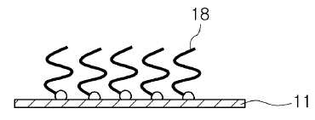
도 2는 본 발명의 일 구현예에 따른 금속 극박재 상에 자기조립 단분자막을 형성한 개념을 개략적으로 나타낸 개념도이다.
도 3은 본 발명의 일 구현예에 따른 전기주조법에 사용되는 모판의 일예를 개략적으로 도시한 도면이다.
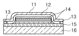
도 4는 본 발명의 일 구현예에 따른 봉합재에 의해 유기전자소자를 봉지한 단면을 개략적으로 나타낸 도면이다.
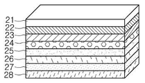
도 5는 본 발명의 일 실시예에 따른 봉지 시험을 우한 유기발광소자의 구조를 개략적으로 나타낸 도면이다.
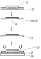
도 6은 본 발명의 실시예에 따라 봉합재를 제조하고, 상기 봉합재를 사용하여 유기전자소자를 봉지하는 공정을 개략적으로 나타낸 도면이다.

12: 탄성고분자 코팅층 13: 경화성 유기 결합제
14: 유기전자소자 15: 제 1 전극(anode)
16: 기판 17: 자기조립 단분자막
20: 모판
21: 제2 전극 22: 전자 주입층
23: 전자 수송층 24: 발광층
25: 정공 수송층 26: 정공 주입층
27: 제1 전극 28: 유리
Claims (19)
- 기판상에 위치하는 유기전자소자를 봉지하는 봉합재로서,
상기 봉합재는 상기 유기전자소자가 수용되는 수용부 및 상기 기판과 대면하여 밀봉하는 접합부를 포함하는 봉합재.
- 제 1항에 있어서, 상기 봉합재는 금속 극박재 및 상기 수용부가 형성되는 금속 극박재의 일면에 형성된 탄성 고분자 코팅층을 포함하며, 상기 탄성 고분자 코팅층은 상기 수용부 내부에 형성되는 것인 봉합재.
- 제 1항에 있어서, 상기 수용부는 25 내지 30㎛의 깊이를 갖는 것인 봉합재.
- 제 2항에 있어서, 상기 금속 극박재는 30-100㎛의 두께를 갖는 것인 봉합재.
- 제 2항에 있어서, 상기 금속 극박재는 Fe-Ni 합금인 봉합재.
- 제 5항에 있어서, 상기 Fe-Ni 합금은 Ni 함량이 32~38중량%이고, 잔부 Fe 및 기타 불가피한 불순물을 포함하는 봉합재.
- 제 2항에 있어서, 상기 탄성 고분자 코팅층은 실리콘 고분자, 폴리이소프렌, 천연고무, 폴리부타디엔, 폴리우레탄 및 이들의 유도체로부터 선택되는 하나 또는 2 이상의 혼합물인 봉합재.
- 제 2항에 있어서, 상기 탄성 고분자 코팅층은 0.1 내지 1000㎛의 두께를 갖는 것인 봉합재.
- 제 2항에 있어서, 상기 봉합재는 상기 금속 극박재 및 상기 탄성 고분자 코팅층 사이에 자기조립성의 자기조립 단분자막을 더 포함하는 봉합재.
- 제 9항에 있어서, 상기 자기조립 단분자막은 에폭시기 및 트리클로로실란 관능기를 양말단에 갖는 화합물인 봉합재.
- 전기주조에 의해 모판 상에 금속 전착층을 형성한 후 박리하여 금속 극박재를 형성하는 단계; 및
상기 금속 극박재의 일면에 탄성 고분자를 도포하여 탄성 고분자 코팅층을 형성하는 단계
를 포함하는 유기전자소자 봉지용 봉합재 제조방법.
- 제 11항에 있어서, 상기 모판은 상기 봉합재에 봉지되는 유기전자소자의 형상에 대응하는 양각 또는 음각이 형성되며, 상기 금속 극박재는 전기주조에 의해 상기 유기전자소자를 수용하는 수용부가 형성되는 것인 유기전자소자 봉지용 봉합재 제조방법.
- 제 11항에 있어서, 상기 탄성 고분자 코팅층을 형성하기 전에 자기조립성을 갖는 자기조립 단분자막을 형성하는 단계를 더 포함하는 유기전자소자 봉지용 봉합재 제조방법.
- 제 13항에 있어서, 상기 자기조립 단분자막은 상기 탄성 고분자 코팅층이 형성되는 상기 금속 극박재의 일면을 UV 오존 처리하여 -OH기를 형성하고, 양 말단에 에폭시 및 트리클로로실란 관능기를 포함하는 화합물로 표면 개질하여 형성되는 것인 유기전자소자 봉지용 봉합재 제조방법.
- 금속 극박재 및 상기 금속 극박재 표면에 탄성 고분자 코팅층이 형성되며, 상기 탄성 고분자 코팅층이 형성된 면에 유기전자소자가 수용되는 수용부 및 상기 기판과 대면하여 밀봉하는 접합부를 포함하는 봉합재를 준비하는 단계;
상기 접합부의 가장자리에 경화성 유기 결합제를 도포하는 단계; 및
기판 위에 위치한 유기전자소자와 상기 봉합재의 탄성고분자층이 대면하도록 상기 봉합재를 덮고, 상기 경화성 유기 결합제를 경화하여 봉지하는 단계
를 포함하는, 유기전자소자의 봉지방법.
- 제 15항에 있어서, 상기 봉합재는 상기 금속 극박재와 상기 탄성 고분자 코팅층 사이에 에폭시기와 트리클로로실란기를 양 말단에 갖는 화합물에 의한 자기조립 단분자막을 갖는 것인 유기전자소자의 봉지방법.
- 제 15항에 있어서, 상기 경화성 유기 결합재는 열경화성 수지 또는 광경화성 수지인 유기전자소자의 봉지방법.
- 제 15항에 있어서, 상기 경화하는 단계는 롤투롤 공정에 의해 수행되되, 상기 롤의 전, 후 또는 전후에 가압하면서 가열 또는 광조사가 행해지는 유기전자소자의 봉지방법.
- 기판,
상기 기판상에 배치된 유기전자소자 및
상기 유기전자소자를 봉지하는 제 1항 내지 제 10항 중 어느 한 항에 기재된 봉합재를 포함하며,
상기 봉합재는 봉합재의 일면에 형성된 탄성 고분자 층이 유기전자소자와 접하는 봉합재로 봉지된 유기전자소자.
Priority Applications (1)
| Application Number | Priority Date | Filing Date | Title |
|---|---|---|---|
| KR20120112588A KR101482313B1 (ko) | 2012-10-10 | 2012-10-10 | 유기전자소자 봉지용 봉합재, 봉합재 제조방법, 봉지방법 및 봉지된 유기전자소자 |
Applications Claiming Priority (1)
| Application Number | Priority Date | Filing Date | Title |
|---|---|---|---|
| KR20120112588A KR101482313B1 (ko) | 2012-10-10 | 2012-10-10 | 유기전자소자 봉지용 봉합재, 봉합재 제조방법, 봉지방법 및 봉지된 유기전자소자 |
Publications (2)
| Publication Number | Publication Date |
|---|---|
| KR20140046292A true KR20140046292A (ko) | 2014-04-18 |
| KR101482313B1 KR101482313B1 (ko) | 2015-01-13 |
Family
ID=50653324
Family Applications (1)
| Application Number | Title | Priority Date | Filing Date |
|---|---|---|---|
| KR20120112588A Active KR101482313B1 (ko) | 2012-10-10 | 2012-10-10 | 유기전자소자 봉지용 봉합재, 봉합재 제조방법, 봉지방법 및 봉지된 유기전자소자 |
Country Status (1)
| Country | Link |
|---|---|
| KR (1) | KR101482313B1 (ko) |
Cited By (5)
| Publication number | Priority date | Publication date | Assignee | Title |
|---|---|---|---|---|
| WO2016010216A1 (ko) * | 2014-07-15 | 2016-01-21 | 주식회사 포스코 | 유기전자소자 봉지용 유연 봉지재, 상기 봉지재에 의해 봉지된 유기전자소자 및 상기 유기전자소자의 봉지방법 |
| KR20170014709A (ko) * | 2015-07-31 | 2017-02-08 | 엘지디스플레이 주식회사 | 유기발광 표시장치 |
| US9893313B2 (en) | 2015-06-19 | 2018-02-13 | Samsung Display Co., Ltd. | Organic luminescence display device and method of manufacturing the same |
| CN111033786A (zh) * | 2017-08-24 | 2020-04-17 | 张衍 | Oled封装材、其制造方法以及oled封装方法 |
| WO2020191859A1 (zh) * | 2019-03-27 | 2020-10-01 | 武汉华星光电半导体显示技术有限公司 | 一种有机发光二极管显示面板、显示模组及电子装置 |
Family Cites Families (3)
| Publication number | Priority date | Publication date | Assignee | Title |
|---|---|---|---|---|
| KR100652034B1 (ko) * | 2000-10-06 | 2006-11-30 | 엘지전자 주식회사 | 유기 el 디스플레이 소자의 실 커버 플레이트 및 실링방법 |
| JP2002319485A (ja) * | 2001-04-23 | 2002-10-31 | Nisshin Steel Co Ltd | 有機el素子用封止部材 |
| JP4254154B2 (ja) * | 2002-08-13 | 2009-04-15 | パナソニック電工株式会社 | 有機電界発光素子の封止方法 |
-
2012
- 2012-10-10 KR KR20120112588A patent/KR101482313B1/ko active Active
Cited By (7)
| Publication number | Priority date | Publication date | Assignee | Title |
|---|---|---|---|---|
| WO2016010216A1 (ko) * | 2014-07-15 | 2016-01-21 | 주식회사 포스코 | 유기전자소자 봉지용 유연 봉지재, 상기 봉지재에 의해 봉지된 유기전자소자 및 상기 유기전자소자의 봉지방법 |
| US9893313B2 (en) | 2015-06-19 | 2018-02-13 | Samsung Display Co., Ltd. | Organic luminescence display device and method of manufacturing the same |
| US10673015B2 (en) | 2015-06-19 | 2020-06-02 | Samsung Display Co., Ltd. | Organic luminescence display device and method of manufacturing the same |
| KR20170014709A (ko) * | 2015-07-31 | 2017-02-08 | 엘지디스플레이 주식회사 | 유기발광 표시장치 |
| CN111033786A (zh) * | 2017-08-24 | 2020-04-17 | 张衍 | Oled封装材、其制造方法以及oled封装方法 |
| CN111033786B (zh) * | 2017-08-24 | 2022-11-25 | 张衍 | Oled封装材、其制造方法以及oled封装方法 |
| WO2020191859A1 (zh) * | 2019-03-27 | 2020-10-01 | 武汉华星光电半导体显示技术有限公司 | 一种有机发光二极管显示面板、显示模组及电子装置 |
Also Published As
| Publication number | Publication date |
|---|---|
| KR101482313B1 (ko) | 2015-01-13 |
Similar Documents
| Publication | Publication Date | Title |
|---|---|---|
| KR100889625B1 (ko) | 접합방법 및 그를 이용한 유기전계발광표시장치의 제조방법 | |
| US7274141B2 (en) | Inverted organic light emitting diode with doped layers | |
| JP5478908B2 (ja) | 有機発光素子 | |
| US7950567B2 (en) | Organic light emitting diode display device and method of fabricating the same | |
| US8912018B2 (en) | Manufacturing flexible organic electronic devices | |
| US8168967B2 (en) | Organic light emitting device and method of manufacturing the same | |
| EP1913798B1 (en) | Organic light emitting device and method for manufacturing the same | |
| KR101482313B1 (ko) | 유기전자소자 봉지용 봉합재, 봉합재 제조방법, 봉지방법 및 봉지된 유기전자소자 | |
| US20090167159A1 (en) | Organic light emitting device | |
| EP2728635A1 (en) | Top-emitting organic light-emitting device and method for preparing the same | |
| CN102097595A (zh) | 有机发光设备及制造有机发光设备的方法 | |
| CN101128074A (zh) | 一种有机电致发光器件及其制备方法 | |
| EP2728636A1 (en) | Top-emitting flexible organic light emission diode device and preparation method thereof | |
| WO2008027132A1 (en) | Charge transforting layer for organic electroluminescent device | |
| CN103427029A (zh) | 柔性有机发光器件及其制备方法 | |
| KR101056432B1 (ko) | 유기 전계 발광 표시장치 및 이의 밀봉용 충전재 | |
| KR101727887B1 (ko) | 유기전자장치의 제조 방법 | |
| KR101234335B1 (ko) | 유기전자소자의 봉지방법, 봉지된 유기전자소자 및 봉합재 | |
| EP2728637A1 (en) | Top-emitting organic electroluminescent device and manufacturing method thereof | |
| US8916398B2 (en) | Encapsulated structure of light-emitting device, encapsulating process thereof and display device comprising encapsulated structure | |
| WO2011132631A1 (ja) | 有機エレクトロルミネッセンスパネルの製造方法及びその製造方法で製造された有機エレクトロルミネッセンスパネル | |
| JPH11224771A (ja) | 有機エレクトロルミネッセンス素子 | |
| CN104040748A (zh) | 有机电致发光器件及其制备方法 | |
| US9196864B2 (en) | Encapsulated structure of light-emitting device, encapsulating process thereof and display device comprising encapsulated structure | |
| JP2002190384A (ja) | 電界発光素子 |
Legal Events
| Date | Code | Title | Description |
|---|---|---|---|
| A201 | Request for examination | ||
| PA0109 | Patent application |
St.27 status event code: A-0-1-A10-A12-nap-PA0109 |
|
| PA0201 | Request for examination |
St.27 status event code: A-1-2-D10-D11-exm-PA0201 |
|
| E902 | Notification of reason for refusal | ||
| PE0902 | Notice of grounds for rejection |
St.27 status event code: A-1-2-D10-D21-exm-PE0902 |
|
| E13-X000 | Pre-grant limitation requested |
St.27 status event code: A-2-3-E10-E13-lim-X000 |
|
| P11-X000 | Amendment of application requested |
St.27 status event code: A-2-2-P10-P11-nap-X000 |
|
| P13-X000 | Application amended |
St.27 status event code: A-2-2-P10-P13-nap-X000 |
|
| PG1501 | Laying open of application |
St.27 status event code: A-1-1-Q10-Q12-nap-PG1501 |
|
| E902 | Notification of reason for refusal | ||
| PE0902 | Notice of grounds for rejection |
St.27 status event code: A-1-2-D10-D21-exm-PE0902 |
|
| E13-X000 | Pre-grant limitation requested |
St.27 status event code: A-2-3-E10-E13-lim-X000 |
|
| P11-X000 | Amendment of application requested |
St.27 status event code: A-2-2-P10-P11-nap-X000 |
|
| P13-X000 | Application amended |
St.27 status event code: A-2-2-P10-P13-nap-X000 |
|
| E701 | Decision to grant or registration of patent right | ||
| PE0701 | Decision of registration |
St.27 status event code: A-1-2-D10-D22-exm-PE0701 |
|
| GRNT | Written decision to grant | ||
| PR0701 | Registration of establishment |
St.27 status event code: A-2-4-F10-F11-exm-PR0701 |
|
| PR1002 | Payment of registration fee |
St.27 status event code: A-2-2-U10-U11-oth-PR1002 Fee payment year number: 1 |
|
| PG1601 | Publication of registration |
St.27 status event code: A-4-4-Q10-Q13-nap-PG1601 |
|
| FPAY | Annual fee payment |
Payment date: 20180104 Year of fee payment: 4 |
|
| PR1001 | Payment of annual fee |
St.27 status event code: A-4-4-U10-U11-oth-PR1001 Fee payment year number: 4 |
|
| R18-X000 | Changes to party contact information recorded |
St.27 status event code: A-5-5-R10-R18-oth-X000 |
|
| PR1001 | Payment of annual fee |
St.27 status event code: A-4-4-U10-U11-oth-PR1001 Fee payment year number: 5 |
|
| R18-X000 | Changes to party contact information recorded |
St.27 status event code: A-5-5-R10-R18-oth-X000 |
|
| R18-X000 | Changes to party contact information recorded |
St.27 status event code: A-5-5-R10-R18-oth-X000 |
|
| FPAY | Annual fee payment |
Payment date: 20200107 Year of fee payment: 6 |
|
| PR1001 | Payment of annual fee |
St.27 status event code: A-4-4-U10-U11-oth-PR1001 Fee payment year number: 6 |
|
| PR1001 | Payment of annual fee |
St.27 status event code: A-4-4-U10-U11-oth-PR1001 Fee payment year number: 7 |
|
| PR1001 | Payment of annual fee |
St.27 status event code: A-4-4-U10-U11-oth-PR1001 Fee payment year number: 8 |
|
| R18-X000 | Changes to party contact information recorded |
St.27 status event code: A-5-5-R10-R18-oth-X000 |
|
| PN2301 | Change of applicant |
St.27 status event code: A-5-5-R10-R11-asn-PN2301 |
|
| PN2301 | Change of applicant |
St.27 status event code: A-5-5-R10-R14-asn-PN2301 |
|
| P22-X000 | Classification modified |
St.27 status event code: A-4-4-P10-P22-nap-X000 |
|
| PR1001 | Payment of annual fee |
St.27 status event code: A-4-4-U10-U11-oth-PR1001 Fee payment year number: 9 |
|
| R18-X000 | Changes to party contact information recorded |
St.27 status event code: A-5-5-R10-R18-oth-X000 |
|
| P22-X000 | Classification modified |
St.27 status event code: A-4-4-P10-P22-nap-X000 |
|
| R18-X000 | Changes to party contact information recorded |
St.27 status event code: A-5-5-R10-R18-oth-X000 |
|
| PR1001 | Payment of annual fee |
St.27 status event code: A-4-4-U10-U11-oth-PR1001 Fee payment year number: 10 |
|
| PR1001 | Payment of annual fee |
St.27 status event code: A-4-4-U10-U11-oth-PR1001 Fee payment year number: 11 |
|
| R18 | Changes to party contact information recorded |
Free format text: ST27 STATUS EVENT CODE: A-5-5-R10-R18-OTH-X000 (AS PROVIDED BY THE NATIONAL OFFICE) |
|
| R18-X000 | Changes to party contact information recorded |
St.27 status event code: A-5-5-R10-R18-oth-X000 |
|
| P22-X000 | Classification modified |
St.27 status event code: A-4-4-P10-P22-nap-X000 |