KR20140046292A - Encapsulant for packaging an organic electric device, method for preparing the same, method for encapsulating the organic electric device by using the same and organic electric device packaged by the same - Google Patents
Encapsulant for packaging an organic electric device, method for preparing the same, method for encapsulating the organic electric device by using the same and organic electric device packaged by the same Download PDFInfo
- Publication number
- KR20140046292A KR20140046292A KR1020120112588A KR20120112588A KR20140046292A KR 20140046292 A KR20140046292 A KR 20140046292A KR 1020120112588 A KR1020120112588 A KR 1020120112588A KR 20120112588 A KR20120112588 A KR 20120112588A KR 20140046292 A KR20140046292 A KR 20140046292A
- Authority
- KR
- South Korea
- Prior art keywords
- organic electronic
- electronic device
- encapsulant
- elastic polymer
- coating layer
- Prior art date
- Legal status (The legal status is an assumption and is not a legal conclusion. Google has not performed a legal analysis and makes no representation as to the accuracy of the status listed.)
- Granted
Links
Images


Classifications
-
- H—ELECTRICITY
- H10—SEMICONDUCTOR DEVICES; ELECTRIC SOLID-STATE DEVICES NOT OTHERWISE PROVIDED FOR
- H10K—ORGANIC ELECTRIC SOLID-STATE DEVICES
- H10K50/00—Organic light-emitting devices
- H10K50/80—Constructional details
- H10K50/84—Passivation; Containers; Encapsulations
-
- H—ELECTRICITY
- H05—ELECTRIC TECHNIQUES NOT OTHERWISE PROVIDED FOR
- H05B—ELECTRIC HEATING; ELECTRIC LIGHT SOURCES NOT OTHERWISE PROVIDED FOR; CIRCUIT ARRANGEMENTS FOR ELECTRIC LIGHT SOURCES, IN GENERAL
- H05B33/00—Electroluminescent light sources
- H05B33/02—Details
- H05B33/04—Sealing arrangements, e.g. against humidity
-
- H—ELECTRICITY
- H10—SEMICONDUCTOR DEVICES; ELECTRIC SOLID-STATE DEVICES NOT OTHERWISE PROVIDED FOR
- H10K—ORGANIC ELECTRIC SOLID-STATE DEVICES
- H10K50/00—Organic light-emitting devices
- H10K50/80—Constructional details
- H10K50/84—Passivation; Containers; Encapsulations
- H10K50/841—Self-supporting sealing arrangements
-
- H—ELECTRICITY
- H10—SEMICONDUCTOR DEVICES; ELECTRIC SOLID-STATE DEVICES NOT OTHERWISE PROVIDED FOR
- H10K—ORGANIC ELECTRIC SOLID-STATE DEVICES
- H10K50/00—Organic light-emitting devices
- H10K50/80—Constructional details
- H10K50/84—Passivation; Containers; Encapsulations
- H10K50/842—Containers
- H10K50/8423—Metallic sealing arrangements
-
- H—ELECTRICITY
- H10—SEMICONDUCTOR DEVICES; ELECTRIC SOLID-STATE DEVICES NOT OTHERWISE PROVIDED FOR
- H10K—ORGANIC ELECTRIC SOLID-STATE DEVICES
- H10K50/00—Organic light-emitting devices
- H10K50/80—Constructional details
- H10K50/84—Passivation; Containers; Encapsulations
- H10K50/844—Encapsulations
-
- H—ELECTRICITY
- H10—SEMICONDUCTOR DEVICES; ELECTRIC SOLID-STATE DEVICES NOT OTHERWISE PROVIDED FOR
- H10K—ORGANIC ELECTRIC SOLID-STATE DEVICES
- H10K71/00—Manufacture or treatment specially adapted for the organic devices covered by this subclass
Landscapes
- Physics & Mathematics (AREA)
- Optics & Photonics (AREA)
- Engineering & Computer Science (AREA)
- Manufacturing & Machinery (AREA)
- Electroluminescent Light Sources (AREA)
Abstract
본 발명은 플렉서블 OLED 디스플레이에 사용되는 Fe-Ni합금 기판을 전기주조법으로 제조하고, 연속적으로 전해연마를 통하여 표면 조도가 우수한 기판을 제조하는 방법에 관한 것이다. 특히, 본 발명은 전기주조법을 활용하여 기존의 압연 공정에 비하여 단순한 공정으로도 기판을 제조할 수 있기 때문에, 생산성이 뛰어나며, 기판의 박막화를 용이하게 달성 할 수 있으며, 전해연마를 이용하여 나노급 표면 조도를 경제적으로 확보할 수 있다. 본 발명에 의한 금속 기판을 사용하여 OLED를 제조할 경우 OLED의 수명 특성에 큰 영향을 미치는 수분 방지특성이 매우 우수하며 방열특성이 뛰어나기 때문에 OLED 소자의 수명을 크게 늘릴 수 있다.The present invention relates to a method for manufacturing an Fe-Ni alloy substrate used for a flexible OLED display by electroforming and successively performing electrolytic polishing to obtain a substrate having excellent surface roughness. In particular, since the present invention can manufacture a substrate by a simple process as compared to a conventional rolling process by utilizing an electroforming method, it is excellent in productivity, can easily achieve thinning of a substrate, The surface roughness can be economically secured. When the OLED is manufactured using the metal substrate according to the present invention, the OLED device has an excellent moisture-preventing characteristic, which greatly affects the life characteristics of the OLED, and has excellent heat dissipation characteristics.
Description
본 발명은 유기전자소자의 봉지를 위한 봉합재, 상기 봉합재에 의해 봉지된 유기전자소자 및 상기 유기전자소자의 봉지방법에 관한 것이다.
The present invention relates to a sealing material for sealing an organic electronic device, an organic electronic device sealed by the sealing material, and a sealing method of the organic electronic device.
유연성을 갖는 유기전자소자가 차세대 디스플레이로서 국제적으로 주목을 받고 있다. 그러나, 이러한 유기전자소자는 대기 조건에서 수분이나 산소 분자와 반응하여 쉽게 열화될 수 있다는 문제점이 있다. 이에, 공기 중의 분자들로부터 이와 같은 열화를 방지하기 위해, 딱딱한 커버 글라스를 사용하여 통상 유기전자소자를 봉지(encapsulation)하고 있다.
Flexible organic electronic devices are attracting international attention as next generation displays. However, such an organic electronic device has a problem that it can be easily deteriorated by reacting with moisture or oxygen molecules in an atmospheric condition. In order to prevent such deterioration from molecules in the air, a hard cover glass is usually used to encapsulate an organic electronic device.
상기 봉지 공정은 소자의 내구성 향상을 위해 최근 유기 소자에서 반드시 필요한 과정이 되었다. 그러나 딱딱한 커버 글라스와 다량의 흡습제(desiccants)를 사용하는 종래의 봉지 기술은 커버 글라스의 비-유연성, 흡습제의 사용 및 롤투롤(roll-to-roll) 공정과의 비양립성과 같은 치명적인 단점을 가지고 있다.
The sealing process has become a necessary process in organic devices recently to improve the durability of the device. However, conventional encapsulation techniques using rigid cover glasses and large amounts of desiccants have a fatal disadvantage, such as non-flexibility of the cover glass, use of a desiccant, and incompatibility with a roll-to-roll process have.
일반적으로, 종래의 봉지 방법으로는 전통적인 유리 리드를 사용하는 봉지, 원자층 증착법(ALD; atomic layer deposition)에 의한 박막 봉지, 적층 배리어 코팅 리드 및 과불소화된(perfluorinated) 고분자에 의한 봉지 등 다양한 형태의 봉지법이 사용되고 있다.
In general, conventional encapsulation methods include various forms such as encapsulation using conventional glass leads, thin film encapsulation by atomic layer deposition (ALD), laminated barrier coating leads, and encapsulation by perfluorinated polymers Is used.
상기 유리 리드(lid)를 사용하는 일반적인 봉지 방법은 수분 흡수를 위해 게터(getter)를 사용하여 불활성 분위기에서 유기 소자를 봉지하며, 그리고 나서, 소자를 모두 제작한 후에 UV-경화 에폭시 수지로 봉인하는 공정을 추가로 수행하는 방법에 의해 완성된다.
A typical encapsulation method using the glass lid is to encapsulate the organic device in an inert atmosphere using a getter for moisture absorption and then seal the encapsulation with a UV-cured epoxy resin after all the devices are fabricated And the process is further carried out.
한편, 유연한 소자를 위한 봉지의 형태로는 스핀 코팅 및 ALD에 의한 박막 형태가 있다. 이와 같은 박막 봉지 방법의 장점으로는 얇은 형태, 유연성, 및 마모 손상에 대한 내구성을 들 수 있으나, 이 공정은 유해 용매와의 접촉이 요구되며, 상대적으로 낮은 온도에서 수행되어야 한다.
On the other hand, there are spin coating and thin film type by ALD for the flexible device. Advantages of such a thin film encapsulation method include thin shape, flexibility, and durability against abrasion damage, but this process requires contact with harmful solvents and should be performed at a relatively low temperature.
실제로, 상술한 방법들은 약간 복잡하고 진공 조건이 필요하며 다층 증착으로 인하여 소자 봉지에 장시간이 소요된다. 따라서, 유연한 디스플레이 제조를 위해 기술이 변화해 가고 있는 IT 업계의 경향을 반영하면서, 간단하고 용이하면서도 단시간이 소요되는 신규한 봉지 방법을 개발할 필요성이 있다.
In fact, the above-described methods are somewhat complicated and require vacuum conditions, and it takes a long time to encapsulate the device due to multilayer deposition. Therefore, there is a need to develop a simple, easy, and time-consuming new sealing method reflecting the tendency of the IT industry to change the technology for flexible display manufacturing.
본 발명의 일 측면은 흡습제를 사용하지 않고 진공 조건이 필요하지 않아 소자의 제조 공정이 단순화된 신규한 유기전자소자의 봉지를 위한 봉합재를 제공하고자 한다.
One aspect of the present invention is to provide a sealing material for sealing a novel organic electronic device in which the manufacturing process of the device is simplified because a vacuum condition is not required without using a moisture absorbent.
본 발명의 다른 측면은 전기주조법을 통하여 롤투롤 공정에 적합하고, 일체 성형을 통해 수분 투과를 최소화하여 외부 환경에 대한 저항성이 강하고, 우수한 열분산성 및 장기 안정성이 개선된 유기전자소자 봉지용 봉합재를 제공하고자 한다.
Another aspect of the present invention is to provide an organic electronic device encapsulating material which is suitable for a roll-to-roll process through an electroforming process, minimizes water permeation through integral molding, has a strong resistance to the external environment, ≪ / RTI >
또한, 본 발명은 상기 봉합재를 사용하여 유기전자소자를 봉지하는 방법을 제공하고자 한다.
The present invention also provides a method for encapsulating an organic electronic device using the sealing material.
나아가, 본 발명은 상기 봉합재에 의해 봉지된 유기전자소자를 제공한다.
Furthermore, the present invention provides an organic electronic device encapsulated by the sealant.
그러나, 본 발명이 해결하고자 하는 과제는 이상에서 언급한 과제로 제한되지 않으며, 언급되지 않은 또 다른 과제들은 아래의 기재로부터 당업자에게 명확하게 이해될 수 있을 것이다.
However, the problems to be solved by the present invention are not limited to the above-mentioned problems, and other problems not mentioned can be clearly understood by those skilled in the art from the following description.
본 발명은 기판상에 위치하는 유기전자소자를 봉지하는 봉합재에 관한 것으로서, 일 구현예에 따르면, 상기 봉합재는 상기 유기전자소자가 수용되는 수용부 및 상기 기판과 대면하여 밀봉하는 접합부를 포함하는 봉합재를 제공한다.According to one embodiment, the sealing member includes a receiving portion in which the organic electronic device is accommodated, and a sealing portion which is sealed to face the substrate, according to an embodiment of the present invention. Thereby providing a sealing material.
상기 봉합재는 금속 극박재 및 상기 수용부가 형성되는 금속 극박재의 일면에 형성된 탄성 고분자 코팅층을 포함하며, 상기 탄성 고분자 코팅층은 상기 수용부 내부에 형성되는 봉합재일 수 있다.The sealing material may include an elastic polymer coating layer formed on one side of the metal electrode layer and the metal electrode layer on which the receiving portion is formed, and the elastic polymer coating layer may be a sealing material formed in the receiving portion.
상기 수용부는 25 내지 30㎛의 깊이를 갖는 것이 바람직하다.The receiving portion preferably has a depth of 25 to 30 mu m.
또한, 상기 금속 극박재는 30-100㎛의 두께를 갖는 것이 바람직하다. In addition, it is preferable that the metal electrode layer has a thickness of 30-100 mu m.
상기 금속 극박재는 Fe-Ni 합금일 수 있으며, 보다 바람직하게는 Ni 함량이 32~38중량%이고, 잔부 Fe 및 기타 불가피한 불순물을 포함하는 것일 수 있다.The metal foil may be an Fe-Ni alloy, more preferably a Ni content of 32 to 38% by weight, and the balance Fe and other unavoidable impurities.
한편, 상기 탄성 고분자 코팅층은 실리콘 고분자, 폴리이소프렌, 천연고무, 폴리부타디엔, 폴리우레탄 및 이들의 유도체로부터 선택되는 하나 또는 2 이상의 혼합물일 수 있으며, 0.1 내지 1000㎛의 두께로 형성될 수 있다.Meanwhile, the elastic polymer coating layer may be a mixture of one or more selected from silicone polymers, polyisoprene, natural rubber, polybutadiene, polyurethane and derivatives thereof, and may be formed to a thickness of 0.1 to 1000 탆.
상기 봉합재는 상기 금속 극박재 및 상기 탄성 고분자 코팅층 사이에 자기조립성의 자기조립 단분자막을 더 포함할 수 있으며, 상기 자기조립 단분자막은 에폭시기 및 트리클로로실란 관능기를 양말단에 갖는 화합물일 수 있다.
The sealing material may further comprise a self-assembled self-assembled monolayer between the metal pole layer and the elastic polymer coating layer, and the self-assembled monolayer may be a compound having both an epoxy group and a trichlorosilane functional group at both ends.
또한, 본 발명은 유기전자소자 봉지용 봉합재 제조방법에 관한 것으로서, 전기주조에 의해 모판 상에 금속 전착층을 형성한 후 박리하여 금속 극박재를 형성하는 단계, 상기 금속 극박재의 일면에 탄성 고분자를 도포하여 탄성 고분자 코팅층을 형성하는 단계를 포함한다.The present invention also relates to a method for manufacturing a sealing material for encapsulating an organic electronic device, which comprises: forming a metal electrodeposition layer on a base plate by electroforming and then peeling off to form a metal electrode layer; And applying the polymer to form an elastic polymer coating layer.
상기 모판은 상기 봉합재에 봉지되는 유기전자소자의 형상에 대응하는 양각 또는 음각이 형성되며, 상기 금속 극박재는 전기주조에 의해 상기 유기전자소자를 수용하는 수용부가 형성된다.The base plate is formed with an embossed or depressed shape corresponding to the shape of the organic electronic device to be sealed in the sealing material, and the accommodating portion for accommodating the organic electronic device is formed by electroforming the metallic electrode material.
나아가, 상기 탄성 고분자 코팅층을 형성하기 전에 자기조립성을 갖는 자기조립 단분자막을 형성하는 단계를 더 포함할 수 있다. Further, the method may further include forming a self-assembled monolayer having self-assembling property before forming the elastic polymer coating layer.
상기 자기조립 단분자막은 상기 탄성 고분자 코팅층이 형성되는 상기 금속 극박재의 일면을 UV 오존 처리하여 -OH기를 형성하고, 양 말단에 에폭시 및 트리클로로실란 관능기를 포함하는 화합물로 표면 개질하여 형성될 수 있다.
The self-assembled monolayer may be formed by forming a -OH group by UV ozone treatment on one surface of the metal pole layer on which the elastic polymer coating layer is formed, and then surface-modified with a compound containing epoxy and trichlorosilane functional groups at both ends .
한편, 본 발명은 유기전자소자의 봉지방법에 관한 것으로서, 금속 극박재 및 상기 금속 극박재 표면에 탄성 고분자 코팅층이 형성되며, 상기 탄성 고분자 코팅층이 형성된 면에 유기전자소자가 수용되는 수용부 및 상기 기판과 대면하여 밀봉하는 접합부를 포함하는 봉합재를 준비하는 단계, 상기 접합부의 가장자리에 경화성 유기 결합제를 도포하는 단계 및 기판 위에 위치한 유기전자소자와 상기 봉합재의 탄성고분자층이 대면하도록 상기 봉합재를 덮고, 상기 경화성 유기 결합제를 경화하여 봉지하는 단계를 포함한다.According to another aspect of the present invention, there is provided a method of encapsulating an organic electronic device, the method comprising: forming an elastic polymer coating layer on the surface of the metal pole layer and the metal pole layer, Comprising the steps of: preparing a sealing material including a sealing portion facing the substrate; applying a curable organic binder to the edge of the sealing portion; and sealing the sealing material so that the organic electronic element located on the substrate and the elastic polymer layer of the sealing material face each other And curing and sealing the curable organic binder.
상기 봉합재는 상기 금속 극박재와 상기 탄성 고분자 코팅층 사이에 에폭시기와 트리클로로실란기를 양 말단에 갖는 화합물에 의한 자기조립 단분자막을 가질 수 있다.The sealing material may have a self-assembled monolayer made of a compound having epoxy groups and trichlorosilane groups at both terminals between the metal electrode layer and the elastic polymer coating layer.
상기 경화성 유기 결합재는 열경화성 수지 또는 광경화성 수지인 것이 바람직하며, 상기 경화하는 단계는 롤투롤 공정에 의해 수행되되, 상기 롤의 전, 후 또는 전후에 가압하면서 가열 또는 광조사를 행함으로써 봉지할 수 있다.
The curable organic binder is preferably a thermosetting resin or a photo-curable resin. The curing may be performed by a roll-to-roll process, and may be performed by heating or light irradiation while being pressed before, after, have.
나아가, 본 발명은 봉합재로 봉지된 유기전자소자에 관한 것으로서, 기판, 상기 기판상에 배치된 유기전자소자 및 상기 유기전자소자를 봉지하는 상기 봉합재를 포함하며, 상기 봉합재는 봉합재의 일면에 형성된 탄성 고분자 층이 유기전자소자와 접하는 봉합재로 봉지된 유기전자소자를 제공한다.
Further, the present invention relates to an organic electronic device sealed with a sealing material, which comprises a substrate, an organic electronic device disposed on the substrate, and the sealing material for sealing the organic electronic device, wherein the sealing material is provided on one surface of the sealing material And the formed elastic polymer layer is sealed with a sealing material in contact with the organic electronic device.
본 발명의 일 측면에 따르면, 본 발명에 따른 봉합재를 사용함으로써 롤투롤(roll-to-roll) 공정에 적합하고, 나아가 롤투롤 공정에서 소자 제작 공정의 연결선상에서 일체 성형을 통해 유기전자소자를 봉지할 수 있어, 유기전자소자 내로의 수분 투과를 최소화하여 흡습제의 사용을 요구하지 않으며, 진공 조건이 필요하지 않아 유기소자의 봉지 공정을 단순화시킬 수 있으며, 이로 인해 제조비용 및 공정 시간을 절감할 수 있다.
According to one aspect of the present invention, by using the sealing material according to the present invention, it is suitable for a roll-to-roll process. Further, in the roll-to-roll process, The moisture permeation into the organic electronic device can be minimized, so that the use of the desiccant is not required, the vacuum process is not necessary, the sealing process of the organic device can be simplified, and the manufacturing cost and the process time can be reduced .
또한, 본 발명의 다른 측면에 따르면, 본 발명에 따른 봉합재는 열전도율이 우수한 재료를 사용함으로써 열분산성을 향상시킬 수 있어, 유기전자소자의 수명을 증가시킬 수 있다.
Further, according to another aspect of the present invention, the sealing material according to the present invention can improve the thermal diffusivity by using a material having a high thermal conductivity, thereby increasing the lifetime of the organic electronic device.
나아가, 본 발명의 또 다른 측면에 따르면, 금속 소재의 봉합재를 사용함으로써 스크래치 또는 기계적 응력에 대한 저항성이 커, 외부 환경에 대한 저항성이 강하고 장기 안정성이 개선된 유기전자소자를 얻을 수 있다.
According to another aspect of the present invention, there is provided an organic electronic device which is resistant to scratches or mechanical stress, has high resistance to external environment and has improved long-term stability, by using a sealing material made of a metal material.
그러나, 본 발명에 따른 효과는 이상에서 언급한 효과로 제한되지 않으며, 언급되지 않은 또 다른 본 발명에 따른 효과는 아래의 기재로부터 당업자에게 명확하게 이해될 수 있을 것이다.
However, the effects according to the present invention are not limited to the effects mentioned above, and the effects according to the present invention which are not mentioned can be clearly understood by those skilled in the art from the following description.
도 1은 본 발명의 일 구현예에 따른 봉합재의 단면을 개략적으로 나타낸 도면이다.
도 2는 본 발명의 일 구현예에 따른 금속 극박재 상에 자기조립 단분자막을 형성한 개념을 개략적으로 나타낸 개념도이다.
도 3은 본 발명의 일 구현예에 따른 전기주조법에 사용되는 모판의 일예를 개략적으로 도시한 도면이다.
도 4는 본 발명의 일 구현예에 따른 봉합재에 의해 유기전자소자를 봉지한 단면을 개략적으로 나타낸 도면이다.
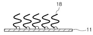
도 5는 본 발명의 일 실시예에 따른 봉지 시험을 우한 유기발광소자의 구조를 개략적으로 나타낸 도면이다.
도 6은 본 발명의 실시예에 따라 봉합재를 제조하고, 상기 봉합재를 사용하여 유기전자소자를 봉지하는 공정을 개략적으로 나타낸 도면이다.BRIEF DESCRIPTION OF THE DRAWINGS FIG. 1 is a schematic cross-sectional view of a seal member according to an embodiment of the present invention. FIG.
2 is a conceptual view schematically showing a concept of forming a self-assembled monolayer on a metal foil according to an embodiment of the present invention.
3 is a view schematically showing an example of a base plate used in the electroforming method according to an embodiment of the present invention.
4 is a schematic cross-sectional view of an organic electronic device encapsulated with a sealing material according to an embodiment of the present invention.
FIG. 5 is a schematic view illustrating the structure of an organic light emitting device according to an embodiment of the present invention. FIG.
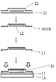
6 is a view schematically showing a step of manufacturing a sealing material according to an embodiment of the present invention and sealing the organic electronic element using the sealing material.
본 발명은 유기전자소자의 봉지를 위한 봉합재, 상기 봉합재를 이용하여 봉지된 유기전자소자 및 상기 봉합재를 사용하여 유기전자소자를 봉합하는 방법에 관한 것으로서, 이하, 도면을 참조하여 보다 구체적으로 설명한다.
BACKGROUND OF THE INVENTION 1. Field of the Invention The present invention relates to a sealing material for sealing an organic electronic device, an organic electronic device sealed using the sealing material, and a method for sealing an organic electronic device using the sealing material, .
도 1은 본 발명의 일 구현예에 따른 봉합재의 단면을 개략적으로 나타낸 도면이며, 도 2는 본 발명의 일 구현예에 따른 금속 극박재 상에 자기조립 단분자막을 형성한 개념을 개략적으로 나타낸 개념도이다. 또한, 도 3은 본 발명의 일 구현예에 따른 전기주조법에 사용되는 모판의 일예를 개략적으로 도시한 도면이며, 그리고, 도 4는 본 발명의 일 구현예에 따른 봉합재에 의해 유기전자소자를 봉지한 단면을 개략적으로 나타낸 도면이다. 나아가, 도 5는 본 발명의 일 실시예에 따른 봉지 시험을 우한 유기발광소자의 구조를 개략적으로 나타낸 도면이다.
FIG. 1 is a schematic view showing a cross-section of a sealing material according to an embodiment of the present invention, and FIG. 2 is a conceptual view schematically showing a concept of forming a self-assembled monolayer on a metal foil according to an embodiment of the present invention . 3 is a view schematically showing an example of a base plate used in an electroforming method according to an embodiment of the present invention, and Fig. 4 is a cross-sectional view of an organic electronic device according to an embodiment of the present invention, 1 is a schematic view showing an encapsulated cross section. 5 is a schematic view illustrating the structure of an organic light emitting device according to an embodiment of the present invention.
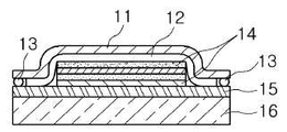
본 발명에 따르면 유기전자소자(14)를 봉지하기 위한 봉합재(10)를 제공한다. 상기 봉합재(10)는 금속으로 된 금속 극박재(11)를 사용하는 것이 바람직하다. 종래에는 유기전자소자(14)를 봉지함에 있어서 유리 등과 같은 단단한 물질을 사용하였으나, 얇은 금속 극박재(11)를 사용함으로써 유연성을 확보할 수 있으며, 열 분산성이 우수한 금속의 성질로 인하여 소자의 수명이 증가할 가능성이 있고, 또 롤투롤(roll-to-roll) 공정에 의해 유기 소자 또는 플렉서블 디스플레이에 보호막을 씌울 수 있다. 나아가, 기존 봉지 재료에 비하여 스크래치, 기계적 응력에 대한 저항성이 크므로 소자의 장기 안정성을 개선할 수 있다.
According to the present invention, a sealing material (10) for sealing an organic electronic device (14) is provided. The sealing
상기 금속 극박재(11)는 이로써 한정되는 것은 아니나, 철, 구리, 은, 니켈, 납, 아연, 주석 및 이들의 합금과 금속으로 이루어지는 그룹으로부터 선택되는 하나 이상을 사용할 수 있다. 바람직하게는 상기 금속 극박재(11)는 철 또는 철계 합금을 사용하는 것이 바람직하다. 이와 같은 철 또는 철계 합금은 본 발명에서 원하는 열분산성이 우수함은 물론, 상대적으로 저가의 금속으로서 경제적인 측면에서 바람직하다.
The
바람직하게는 Fe-Ni 합금을 금속 극박재(11)로 사용할 수 있으며, 보다 바람직하게는 Ni 함량이 32~38중량%이고, 잔부가 Fe 및 기타 불가피한 불순물을 포함하는 것을 사용할 수 있다. 봉합재(10)에 사용되는 물질의 경우 고온공정에서 기판으로 사용되는 물질과 열팽창계수 차이가 클 경우 열응력 등에 의하여 유기전자소자(14)의 파단이 일어날 수 있다. 따라서, 상기와 같이 Ni 함량이 32~38중량%일 경우 기판으로 주로 사용되는 유리의 열팽창계수와 거의 동일한 4×10⁻⁶m/K 이하의 열팽창계수를 가지게 되어, 열응력에 의한 유기전자소자(14)의 파단을 방지할 수 있어 바람직하다.
Preferably, the Fe-Ni alloy can be used as the
상기 금속 극박재(11)의 두께는 휘어질 정도의 두께라면 특별히 한정하지 않으나, 금속 극박재(11)의 두께가 너무 얇으면 구겨질 염려가 있고, 공정상 기판(16)의 핸들링이 어려울 수 있으며, 너무 두꺼우면 금속 극박재(11)를 제조하는 기술에 대비하여 생산성이 떨어지는 단점이 있다. 상기 금속 극박재(11)의 두께는 이와 같은 점을 고려하여, 예를 들어, 30~100㎛ 정도의 두께를 갖는 것이 바람직하다.
The thickness of the
한편, 이와 같은 금속 극박재(11)는 산소 및 수증기에 대하여 투과성을 가지고 있다. 따라서, 상기 금속 극박재(11)의 표면을 통하여 유기전자소자(14) 내부로 산소 및 수증기의 침투를 방지할 필요가 있다. 이를 위해 본 발명의 봉합재(10)는 완충층으로서 탄성 고분자 코팅층(12)을 갖는 것이 바람직하다. 이와 같은 탄성 고분자 코팅층(12)은 수분의 침투를 방지함은 물론, 상기 금속 극박재(11)와 유기전자소자(14) 사이의 압력을 완화하고 스크래치 등의 물리적 손상을 최소화하는 완충층 역할을 한다.
On the other hand, such a
또한, 상기 금속 극박재(11) 자체만으로는 아래에 위치한 기판(16) 등의 층과 자유부피(free volume) 없이 적층 공정을 수행하기가 어렵지만, 상기 탄성 고분자 코팅층(12)을 포함하는 경우에는 반데르발스 인력에 의해 아래의 기판(16)과 정합성 접촉(conformal contact)을 유도하여 밀착시킬 수 있다.
In addition, it is difficult to perform the lamination process without the free volume with the layer of the
이와 같은 탄성 고분자 코팅층(12)은 특별히 한정하는 것은 아니지만, 실리콘계 고분자, 폴리이소프렌, 천연고무, 폴리부타디엔, 폴리우레탄 및 이들의 유도체를 사용하여 형성할 수 있으며, 이들은 단독으로 또는 혼합하여 사용할 수 있다. 이들 중에서, 실리콘계 고분자를 사용하는 것이 바람직하며, 보다 바람직하게는 폴리(디메틸실록산)(PDMS)을 사용할 수 있다.
The elastic
상기 탄성 고분자는 경화제와 혼합하여 상기 금속 극박재(11) 상에 코팅함으로써 가교된 탄성 고분자 코팅층(12)을 형성할 수 있다. 상기 경화제는 탄성 고분자를 경화시킬 수 있는 것이라면 특별히 한정하지 않다. 이와 같은 탄성 고분자와 경화제가 혼합된 것으로는, 예를 들어, 다우코닝사에서 제조 판매되는 Sylgard 184 를 적합하게 사용할 수 있다.
The elastic polymer may be mixed with a curing agent and coated on the
상기 금속 극박재(11) 상에 형성되는 상기 탄성 고분자 코팅층(12)은 특별히 한정하는 것은 아니지만, 0.1 내지 1000㎛ 범위의 두께로 코팅할 수 있으며, 바람직하게는 1 내지 100㎛, 보다 바람직하게는 예를 들어 25 내지 30㎛ 두께로 코팅할 수 있다.
The elastic
탄성고분자와 경화제의 혼합 조성물을 상기 금속 극박재(11) 상에 코팅하는 방법은 특별히 한정하는 것은 아니지만, 얇고 균일한 탄성 고분자 코팅층(12)을 형성하기 위하여 스핀코팅에 의하여 상기 금속 극박재(11) 상에 도포하는 것이 바람직하다. 나아가, 탄성고분자 코팅층(12)의 두께가 1mm 이하, 표면 조도(roughness)를 서브 마이크로 미터 이하로 얇게 조절할 수 있는 방법이라면 상기 스핀코팅 외의 방법이라도 무방하다.
The method of coating the mixed composition of the elastic polymer with the curing agent on the
이때, 상기 탄성 고분자 코팅층(12)과 금속 극박재(11)와의 접착력을 증대시키기 위해 계면 접합층을 개입시킬 수도 있다. 상기 계면 접합층으로는 자기조립 특성을 갖는 자기조립 단분자막(SAM; Self-Assembled Monolayer)(17)을 형성하는 것이 바람직하다. 이와 같은 자기조립 단분자막(17)으로는 예를 들어, 실록산을 사용하여 형성할 수 있다. 즉, 상기 자기조립 단분자막(17)은 이에 한정하는 것은 아니지만, 다음과 같은 구조식을 갖는 에폭시기 및 트리클로로실란 관능기를 양 말단에 포함하는 화합물로 이루어진 것일 수 있다. 상기 금속 극박재(11)를 UV 오존 처리하여 표면에 -OH기의 형성을 유도한 후, 탄화수소 계열로서 양 말단에 에폭시 및 트리클로로실란 관능기를 포함하는, 다음의 화학식과 같은 화합물로 표면을 개질함으로써 자기조립 단분자막(17)을 형성할 수 있다. At this time, an interfacial bonding layer may be interposed in order to increase the adhesive strength between the elastic

본 발명에 있어서는 상기와 같은 봉합재(10)를 사용하여 기판(16) 상의 유기전자소자(14)를 봉지하는데 사용할 수 있다. 이때, 상기 봉합재(10)가 종래와 같이 판상인 경우에는 기판(16) 상의 유기전자소자(14) 상에 봉합재(10)를 적층하고, 상기 봉합재(10)의 가장자리를 압력을 가하여 봉합재(10)를 기판(16)과 밀착시키게 되는데, 이때, 가해지는 압력으로 인해 봉지되는 유기전자소자(14)의 파괴를 초래하는 문제가 발생할 수 있다. 또한, 정밀하게 밀착하더라도 기판(16)과 봉합재(10) 사이에 간격이 생기게 되며, 이와 같은 간극을 통해 수분이 침투하여 장시간 사용시 수명의 열화가 일어나게 된다.
In the present invention, the
따라서 이와 같은 봉합재(10)의 가압 성형 및 기판(16)과 봉합재(10) 간의 간격을 최소화하는 것이 바람직하다. 이를 위해, 본 발명의 봉합재(10)는 봉지되는 유기전자소자(14)의 형상에 대응하는 소정 형상으로 미리 성형되어 있는 것이 바람직하다. 이에 따라 본 발명은 기판(16)상에 위치하는 유기전자소자(14)를 봉지하는 봉합재(10)로서, 상기 유기전자소자(14)가 수용되는 수용부가 미리 형성되어 있는 봉합재(10)를 제안한다. 이를 위해 금속 극박재(11)를 유기전자소자(14)가 수용될 수 있는 수용부가 형성되도록 제작되는 것이 바람직하다.
Therefore, it is preferable to pressurize the sealing
상기 금속 극박재(11)를 제조하는 방법은 특별히 한정하지 않으며, 압연법은 물론, 전주방법에 의해 제조될 수 있다. 압연법에 의해 본 발명의 금속 극박재(11)를 제조하는 경우, 기판(16) 상에 적층되어 봉합재(10)에 의해 봉지되는 유기전자소자(14)의 형상과 일치되도록 스탬핑 등의 방법에 의해 봉합재(10)를 성형할 수 있다.
The method for producing the
그러나, 압연법에 의하는 경우, 봉지되는 유기전자소자(14)의 형상에 정밀하게 대응하도록 금속 극박재(11)를 성형하는 것이 용이하지 않을 수 있는바, 전기주조방법에 의해 금속 극박재(11)를 제조하는 것이 보다 바람직하다. 전기주조방법에 의해 금속 극박재(11)를 제조하는 경우, 모판에 금속을 전착시킬 수 있어, 모판의 형상이 그대로 전사된 금속 극박재(11)를 얻을 수 있으며, 따라서 치수 정밀도를 높일 수 있다.
However, in the case of the rolling method, it may not be easy to form the
또한, 전기주조방법을 적용하는 경우, 모판을 계속적을 사용하여 금속 극박재(11)를 원하는 형상으로 계속적으로 생산할 수 있으며, 롤투롤(roll-to-roll) 공정에 의해 수행되므로 유기전자소자(14)를 봉지하는데 있어서도 연속 공정으로 수행될 수 있어 바람직하다.
Further, in the case of applying the electroforming method, the
상기 전기 주조를 위한 모판(20)으로서는 그 재질을 특별히 한정하는 것은 아니지만, 산화 피막을 갖는 재질을 사용하는 것이 바람직하며, 예를 들어, 금속 스테인레스, 타이타늄 등을 사용할 수 있다.
The material of the
전기주조방법에 의해 금속 극박재(11)를 제조하는 경우에는, 그에 의해 봉지되는 유기전자소자(14) 형상에 일치하는 형상을 갖도록 하기 위해, 모판(20)의 표면을 음각 또는 양각으로 유기전자소자(14)의 형상과 일치되도록 형성함으로써 유기전자소자(14)와 대응되는 수용부를 갖는 금속 극박재(11)를 얻을 수 있다.
In the case of manufacturing the
따라서, 상기 모판(20)은 도 3 또는 도 6에 나타낸 바와 같이 기판(16)상에 적층되는 유기전자소자(14)의 형상과 대응되도록 음각 또는 양각을 형성하는 것이 바람직하다. 도 3에는 모판(20)을 음각으로 형성한 예를 도시하였으며, 도 6는 모판(20)이 양각으로 형성된 예를 도시하였다.
Therefore, it is preferable that the
이때, 상기 수용부의 외측 가장자리는 유기전자소자(14)가 적층되는 기판(16) 또는 기판(16)상의 전극(15)과 대면하여 유기전자소자(14)를 봉지하기 위한 접합부를 포함한다.
At this time, the outer edge of the accommodating portion includes a junction for encapsulating the organic
상기 모판(20)에 음각 또는 양각을 형성하는 것은 레이저 가공에 의해 형성할 수 있으며, 음각 또는 양각을 형성하는 깊이는 봉지되는 유기전자소자(14)에 따라 달라질 수 있으나, 예를 들면 25 내지 30㎛일 수 있다.
The forming depth of the
이와 같은 모판(20)을 사용하여 전기주조에 의해 금속 극박재(11)를 제조하면, 보다 정밀한 치수로 유기전자소자(14)에 대응하는 형상의 수용부를 갖는 금속 극박재(11)를 얻을 수 있으며, 이로 인해 상기 봉합재(10)를 사용하여 유기전자소자(14)를 봉지하는 경우, 봉합재(10)와 기판(16)간의 간격을 최소화할 수 있다. 따라서, 봉합재(10)를 기판(16)에 밀착시키기 위한 압력을 가할 필요성이 줄어들게 되어 유기전자소자(14)의 손상을 억제할 수 있다.
When the
다음으로, 본 발명은 상기와 같은 봉합재(10)를 사용하여 유기전자소자(14)를 봉지하는 방법을 제공한다. 본 발명의 일 측면에 따르면, 상기한 바와 같이 금속 극박재(11) 및 상기 금속 극박재(11) 표면에 탄성 고분자 코팅층(12)이 형성되고, 유기전자소자(14)가 수용되는 수용부 및 접합부를 포함하는 봉합재(10)(encapsulant)를 준비하는 단계, 상기 봉합재(10)의 일부에 경화성 유기 결합제(13)를 도포하는 단계 및 기판(16) 위에 위치한 유기전자소자(14)와 상기 탄성고분자가 접하도록 하여 상기 봉합재(10)로 덮은 상기 유기전자소자(14)를 경화하는 단계를 포함한다.
Next, the present invention provides a method for encapsulating the organic
상기 봉합재(10)에 대하여는 위에서 상술하였는바, 여기서는 설명을 생략한다.
As described above, the sealing
상기와 같은 봉합재(10)를 사용하여 상기와 같은 적층 구조를 갖는 유기전자소자(14)를 봉지할 수 있다. 상기 유기전자소자(14)는 일반적으로 기판(16) 상에 적층된 전극(15) 상에 형성되는 것으로서, 상기 유기전자소자(14)를 상기 봉합재(10)의 수용부에 수용하고, 상기 기판(16) 또는 상기 기판(16) 상의 전극(15)과 봉합재(10)의 접합부를 접합함으로써 봉지할 수 있다. 이하, 접합부와 접합되는 기판(16) 또는 기판(16) 상의 전극(15)을 단순히 기판(16)이라 한다.
The organic
이때, 상기 기판(16) 상의 전극(15)과 봉합재(10)의 접합부 간의 접합은 경화성 유기 결합제(13)를 사용하여 수행하는 것이 바람직하다. 상기 경화성 유기 결합제(13)는 상기 봉합재(10)와 상기 기판(16)이 접합하도록 돕는 역할을 하며, 봉합재(10)와 유기전자소자(14), 그리고 그 하부에 위치한 기판(16)이 적층 구조를 이루면서 서로 분리되지 않도록 한다.
At this time, it is preferable that bonding between the
즉, 기판(16)과 접하는 봉합재(10)의 일부에 경화성 유기 결합제(13)를 도포한 후, 상기 봉합재(10)의 탄성고분자가 기판(16) 상에 위치한 유기전자소자(14)와 접하도록 덮은 후, 상기 경화성 유기 결합제(13)를 경화시킴으로써 유기전자소자(14)를 봉합할 수 있다. 이를 통해 봉합재(10)와 기판(16) 사이에 간격이 발생하는 것을 억제 또는 제거할 수 있다.
That is, after the curable
상기 경화성 유기 결합제(13)는 특별히 한정하는 것은 아니지만, 열경화성 수지(thermal crosslinking resin) 또는 광경화 수지(Photo-curing resin)를 사용할 수 있다. 이와 같은 경화성 유기 결합제(13)에 의하여 봉합재(10)가 기판(16)에 부착되고 탄성 고분자 코팅층(12)이 유기전자소자(14)에 직접 접촉하게 된다.
The curable
상기 열경화성 수지 또는 광경화성 수지는 특별히 한정하는 것은 아니며, 통상적으로 사용될 수 있는 것이라면 본 발명에서도 적용할 수 있는 것으로서, 예를 들어, 상기 열경화성 수지로는 페놀, 멜라민, 에폭시, 폴리에스터 등의 수지를 사용할 수 있으며, 예를 들어 아랄다이트 제품을 사용할 수 있다. 나아가, 상기 광경화성 수지로는 에폭시, 우레탄, 폴리에스터 수지 등을 사용할 수 있으며, 에를 들어, NAGASE사에서 제조 판매되는 XNR5570-B1 등을 들 수 있다.
The thermosetting resin or photocurable resin is not particularly limited and can be applied to the present invention as long as it can be used normally. For example, resins such as phenol, melamine, epoxy, and polyester may be used as the thermosetting resin For example, Araldite products can be used. Furthermore, epoxy, urethane, polyester resin, etc. can be used as said photocurable resin, For example, XNR5570-B1 etc. which are manufactured and sold by NAGASE company are mentioned.
유기전자소자(14)를 본 발명의 봉합재(10)로 봉지하는 과정 중 경화하는 단계에서 열 및 압력을 가하거나, 상기 경화하는 단계 이전 또는 이후에 열 및 압력을 가하는 공정을 더 포함할 수 있으며, 특별히 한정하지 않는다.
It is possible to further include a step of applying heat and pressure during the step of curing the organic
경화처리 방법으로서 열 및 압력을 가하게 되면 금속 극박재(11), 탄성고분자, 유기전자소자(14), 기판(16)으로 이루어진 적층 구조가 더 밀착되어 탈착을 어렵게 만든다. 열을 가하는 공정과 압력을 가하는 공정은 동시에 수행할 수도 있고, 분리해서 수행할 수도 있다. 나아가, 열 이외에도 자외선, 전자선 등 방사선을 활용하여 경화를 촉진할 수도 있다.
When heat and pressure are applied as a curing treatment method, the laminated structure composed of the
상기 열 및 압력을 가하면서 봉합재(10)로 덮은 유기전자소자(14)를 롤(roll)을 지나도록 할 수 있으나, 이에 제한되는 것은 아니다. 유리 등 단단한 물질을 사용하던 종래의 봉지 방법과 달리, 본 발명은 고분자로 코팅된 얇은 금속 극박재(11)를 사용한 봉지 방법이므로 유연성이 있어서, 롤투롤(roll-to-roll) 공정 동안 유기 소자 또는 플렉서블 디스플레이에 보호막을 씌울 수 있으므로 유용한 방법이 될 수 있다.
The organic
상기 롤을 지나가는 공정은 열 및 압력을 가하는 공정과 동시에 수행될 수도 있고, 롤을 지나가는 공정의 전후에 열 및 압력을 가하는 공정을 수행할 수도 있으며, 이를 복합적으로 활용할 수도 있다.
The process of passing the roll may be performed simultaneously with the process of applying heat and pressure, or the process of applying heat and pressure before and after the process of passing the roll may be performed, or the process may be used in combination.
이와 같이, 본 발명의 봉합재(10)는 일체성형을 통하여 유기전자소자(14)를 봉지할 수 있으며, 이에 의해 공기에 노출되는 유기전자소자(14)의 면적을 최소화할 수 있어, 유기전자소자(14)의 안정성에 기여할 수 있다.
As described above, the sealing
다음으로, 본 발명의 봉합재(10)를 사용하여 봉지되는 유기전자소자(14)에 대하여 설명하나, 이는 본 발명의 봉합재(10)가 적용될 수 있는 일 예를 나타내는 것으로서, 이로서 한정되는 것이 아니다.
Next, the organic
상기 기판(16)은 특별히 한정하는 것이 아니며, 유기전자소자(14)에 있어서 기판(16)으로서 일반적으로 사용되는 것이라면 제한없이 사용될 수 있다. 예를 들어, 유리 및 고분자 필름, 플라스틱 등을 사용할 수 있으며, 구체적으로는 폴리에틸렌테레프탈레이트(PET), 폴리에틸렌나프탈렌(PEN), 폴리카보네이트(PC), 폴리이미드(PI) 등을 들 수 있다.
The
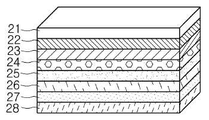
한편, 상기 기판(16) 위에는 유기전자소자(14)가 적층된다. 이와 같은 유기전자소자(14)의 일 예로서 유기발광소자를 들 수 있으며, 상기 유기발광소자를 예로 들어 설명한다. 이와 같은 유기발광소자를 본 발명에 따른 봉합재(10)로 봉지한 예를 도 4에 나타내었다.
On the other hand, an organic
상기 유기발광소자는 제1 전극(27), 제2 전극(21), 및 상기 제1 전극(27)과 상기 제2 전극(21) 사이에 유기층이 개재되며, 상기 유기층은 정공 관련층으로서 정공 주입층(26)(HIL; Hole Injection Layer)(26) 및 정공 수송층(25)(HTL; Hole Transfer Layer)(25), 발광층(24)(EML; Electron Emission Layer)(24), 그리고, 전자관련층으로서, 전자 수송층(ETL; Electron Transfer Layer)(23) 및 전자 주입층(EIL; Electron Injection Layer)(22)을 포함한다.
The organic light emitting device includes a first electrode 27, a
상기 제1 전극(27)의 형성 재료는 특별하게 제한되지는 않으며, 제1 전극(27)이 애노드(anode)인 경우에는 애노드는 정공 주입이 용이한 전도성 금속 또는 그 산화물을 사용할 수 있다. 그 예로서는, 산화인듐주석(Indium Tin Oxide: ITO), 산화인듐아연(Indium Zinc Oxide: IZO), 산화주석(SnO2), 산화아연(ZnO) 또는 그 혼합물, 니켈(Ni), 백금(Pt), 금(Au), 이리듐(Ir) 등을 사용할 수 있다.
The material for forming the first electrode 27 is not particularly limited. When the first electrode 27 is an anode, the anode may use a conductive metal or an oxide thereof, which facilitates hole injection. Examples thereof include indium tin oxide (ITO), indium zinc oxide (IZO), tin oxide (SnO 2 ), zinc oxide (ZnO) or a mixture thereof, nickel (Ni) , Gold (Au), iridium (Ir), or the like.
상기 제2 전극(21)의 형성 재료 역시 특별하게 제한되지는 않으며, 제2 전극(21)이 캐소드(cathode)인 경우에는 낮은 일함수를 갖는 금속, 합금, 전기전도성 화합물 및 이들의 혼합물을 사용할 수 있다. 그 구체적인 예로서는, 리튬(Li), 세슘(Cs), 바륨(Ba), 마그네슘(Mg), 알루미늄(Al), 은(Ag), 칼슘(Ca), 알루미늄-리튬(Al-Li), 마그네슘-인듐(Mg-In), 마그네슘-은(Mg-Ag), 칼슘-알루미늄(Ca-Al), LiF/Ca, LiF/Al, BaF2/Ca이나 이들의 합금 혹은 이들의 다중층 등을 이용하여 형성할 수 있다. 또한 전면 발광소자를 얻기 위하여 ITO, IZO를 사용한 투과형 캐소드를 사용할 수도 있다.
The material for forming the
한편, 상기 정공 관련층 및 전자 관련층은 전자나 정공의 전극(15)으로부터의 주입이나 이동도를 조정한다.
On the other hand, the hole-related layer and the electron-related layer adjust the injection or mobility of the electrons or holes from the
상기 정공 주입층(26)은 전도성 고분자와 불화(fluorinated) 혹은 과불화(perfluorinated) 이오노머(ionomer)로 구성된 조성물로 구비될 수 있다. 상기 정공 주입층(26)에 포함되는 전도성 고분자는 폴리티오펜, PEDOT(폴리(3,4-에틸렌 디옥시티오펜)), 폴리아닐린, 폴리피롤, 폴리아세틸렌, 이들의 유도체 및 셀프-도핑 전도성 고분자로 이루어진 군으로부터 선택된 하나 이상일 수 있다. 상기 정공 주입층(26)을 이루는 물질의 예로서, PEDOT(폴리(3,4-에틸렌디옥시티오펜)):PSS(폴리(스티렌설포네이트))를 들 수 있다.
The hole injection layer 26 may be formed of a conductive polymer and a fluorinated or perfluorinated ionomer. The conductive polymer contained in the hole injection layer 26 may be at least one selected from the group consisting of polythiophene, PEDOT (poly (3,4-ethylenedioxythiophene)), polyaniline, polypyrrole, polyacetylene, derivatives thereof and self- Lt; / RTI > An example of the material forming the hole injection layer 26 is PEDOT (poly (3,4-ethylenedioxythiophene)): PSS (poly (styrenesulfonate)).
상기 정공 주입층(26) 상부로는 발광층(24)이 형성되며, 상기 발광층(24)을 형성하는 물질로는 특별히 제한되지 않으나, 구체적으로는, 옥사디아졸 다이머 염료(oxadiazole dimer dyes (Bis-DAPOXP)), 스피로 화합물(spiro compounds; Spiro-DPVBi, Spiro-6P), 트리아릴아민 화합물(triarylamine compounds), 비스(스티릴)아민(bis(styryl)amine, DPVBi, DSA), 4,4'-비스(9-에틸-3-카바조비닐렌)-1,1'-비페닐(BCzVBi), 페릴렌(perylene), 2,5,8,11-테트라-tert-부틸페릴렌(TPBe), 9H-카바졸-3,3'-(1,4-페닐렌-디-2,1-에텐-디일)비스[9-에틸-(9C)](BCzVB), 4,4-비스[4-(디-p-톨일아미노)스티릴]비페닐(DPAVBi), 4-(디-p-톨일아미노)-4'-[(디-p-톨일아미노)스티릴]스틸벤(DPAVB), 4,4'-비스[4-(디페닐아미노)스티릴]비페닐(BDAVBi),비스(3,5-디플루오로-2-(2-피리딜)페닐-(2-카르복시피리딜)이리듐 III(FIrPic) 등(이상 청색), 3-(2-벤조티아졸일)-7-(디에틸아미노)쿠마린(Coumarin 6), 2,3,6,7-테트라히드로-1,1,7,7,-테트라메틸-1H,5H,11H-10-(2-벤조티아졸일)퀴놀리지노-[9,9a,1gh]쿠마린(C545T), N,N'-디메틸-퀸아크리돈(DMQA), 트리스(2-페닐피리딘)이리듐(III)(Ir(ppy)3) 등(이상 녹색), 테트라페닐나프타센(Tetraphenylnaphthacene)(루브린: Rubrene), 트리스(1-페닐이소퀴놀린)이리듐(III)(Ir(piq)3), 비스(2-벤조[b]티오펜-2-일-피리딘) (아세틸아세토네이트)이리듐(III)(Ir(btp)2(acac)), 트리스(디벤조일메탄)펜안트롤린 유로퓸(III)(Eu(dbm)3(phen)), 트리스[4,4'-디-tert-부틸-(2,2')-비피리딘]루테늄(III) 착물(Ru(dtb-bpy)3·2(PF6)), DCM1, DCM2, Eu(삼불화테노일아세톤: thenoyltrifluoroacetone)3 (Eu(TTA)3, 부틸-6-(1,1,7,7-테트라메틸 줄로리딜-9-에닐)-4H-피란)(butyl-6-(1,1,7,7-tetramethyljulolidyl-9-enyl)-4H-pyran: DCJTB) 등(이상 적색)을 사용할 수 있다. 또한, 고분자 발광 물질로는 페닐렌(phenylene)계, 페닐렌 비닐렌(phenylene vinylene)계, 티오펜(thiophene)계, 플루오렌(fluorene)계 및 스피로플루오렌(spiro-fluorene)계 고분자 등과 같은 고분자와 질소를 포함하는 방향족 화합물 등을 포함할 수 있으나, 이에 한정되는 것은 아니다.
A light emitting layer 24 is formed on the hole injection layer 26 and the material for forming the light emitting layer 24 is not specifically limited and oxadiazole dimer dyes Bis- DAPOXP), spiro compounds (Spiro-DPVBi, Spiro-6P), triarylamine compounds, bis (styryl) amine, DPVBi, -Bis (9-ethyl-3-carbazovinylene) -1,1'-biphenyl (BCzVBi), perylene, 2,5,8,11-tetra-tert- butylperylene (TPBe) , 9H-carbazole-3,3'- (1,4-phenylene-di-2,1-ethen-diyl) bis [9-ethyl- (9C)] (BCzVB), 4,4- - (di-p-tolylamino) styryl] biphenyl (DPAVBi), 4- (di- (BDAVBi), bis (3,5-difluoro-2- (2-pyridyl) phenyl- (2-carboxypyridyl) Iridium III (FIrPic) and the like (ideal blue), 3- (2-benzothiazolyl) -7- (2-benzothiazolyl) quinolinol-2-yl) -carbamic acid tert- (More green), such as [9,9a, 1gh] coumarin (C545T), N, N'-dimethyl-quinacridone (DMQA), tris (2-phenylpyridine) iridium (Rubrene), tris (1-phenylisoquinoline) iridium (III) (Ir (piq) 3), bis (2-benzo [b] thiophen-2-yl-pyridine ) (Acetylacetonate) iridium (III) (Ir (btp) 2 (acac)), tris (dibenzoylmethane) phenanthroline europium III (Di-tert-butyl- (2,2 ') -bipyridine] ruthenium (III) complex (Ru (dtb-bpy) 3.2 (PF6)), DCM1, DCM2, Eu 6- (1,1,7,7-tetramethylglutaridyl-9-enyl) -4H-pyran) (3) 7-tetramethyljulolidyl-9-enyl) -4H-pyran: DCJTB) (ideal red). Examples of the polymer light emitting material include polymers such as phenylene, phenylene vinylene, thiophene, fluorene, and spiro-fluorene polymers. An aromatic compound including a polymer and nitrogen, and the like, but the present invention is not limited thereto.
상기 정공 주입층(26)과 발광층(24) 사이에는 정공 수송층(25)을 형성할 수 있다. 상기 정공 수송층(25)은, 아릴아민 유도체 또는 이를 포함하는 고분자를 포함할 수 있다. 바람직하게는, 상기 정공 수송층(25)은 카바졸 또는 이의 유도체, 페녹사진 또는 이의 유도체, 페노티아진(phenothiazine) 또는 이의 유도체, 또는 카바졸기, 페녹사진기 또는 페노티아진기를 포함하는 고분자를 포함할 수 있다. 더욱 바람직하게는, 정공수송층은 1,3,5-트리카바졸릴벤젠, 4,4'-스카바졸릴비페닐, 폴리비닐카바졸, m-비스카바졸릴페닐, 4,4'-비스카바졸릴-2,2'-디메틸비페닐, 4,4',4"-트리(N-카바졸릴)트리페닐아민, 1,3,5-트리(2-카바졸릴페닐)벤젠, 1,3,5-트리스(2-카바졸릴-5-메톡시페닐)벤젠, 비스(4-카바졸릴페닐)실란, N,N'-비스(3-메틸페닐)-N,N'-디페닐-[1,1-비페닐]-4,4'디아민(TPD), N,N'-디(나프탈렌-1-일)-N,N'-디페닐벤지딘(α-NPD), N,N'-디페닐-N,N'-비스(1-나프틸)-(1,1'-비페닐)-4,4'-디아민(NPB), IDE320(이데미쯔사), 폴리(9,9-디옥틸플루오렌-co-N-(4-부틸페닐)디페닐아민) 및 폴리(9,9-디옥틸플루오렌-co-비스-(4-부틸페닐-비스-N,N-페닐-1,4-페닐렌디아민, 폴리(9,9-디옥틸플루오렌-co-N,N-디(페닐)-N,N-디(3-카보에톡시페닐)벤지딘 및 이들의 유도체로 이루어진 군으로부터 선택된 어느 하나 이상을 포함할 수 있으며, 이에 제한되는 것은 아니다.
A
상기 전자 수송층(23)의 형성 재료로는 옥사졸계 화합물, 이소옥사졸계 화합물, 트리아졸계 화합물, 이소티아졸(isothiazole)계 화합물, 옥사디아졸계 화합물, 티아디아졸(thiadiazole)계 화합물, 페릴렌(perylene)계 화합물, 알루미늄 착물(예를 들어, Alq3(트리스(8-퀴놀리놀라토)-알루미늄(tris(8-quinolinolato)-aluminium), BAlq, SAlq, Almq3), 갈륨 착물(예를 들어, Gaq'2OPiv, Gaq'2OAc, 2(Gaq'2))을 사용할 수 있다. 바람직하게는 비스(10-하이드로벤조[h]퀴놀리나토)베릴륨(BEBQ2: bis(10-hydroxybenzo[h]quinolinato)beryllium), 1,3,5-트리스(N-페닐벤지미다졸-2-일)벤젠 (TPBI: 1,3,5-tris(N-phenylbenzimidazol-2-yl)benzene), 터플루오렌 (E3: terfluorene), 비스(페닐퀴녹살린)(bis(phenylquinoxaline)), 스타버스트 트리스(페닐퀴녹살린)(starburst tris(phenylquinoxaline)) 및 이들의 유도체를 포함할 수 있다.
As the material for forming the electron transport layer 23, oxazole compounds, isoxazole compounds, triazole compounds, isothiazole compounds, oxadiazole compounds, thiadiazole compounds, perylene perylene based compounds, aluminum complexes such as Alq3 (tris (8-quinolinolato) -aluminium), BAlq, SAlq, Almq3, gallium complexes (e.g., Bis (10-hydroxybenzo [h] quinolinato) (BEBQ2: bis (10-hydroxybenzo [h] quinolinato) beryllium), 1,3,5-tris (N-phenylbenzimidazol-2-yl) benzene (TPBI: 1,3,5- : terfluorene, bis (phenylquinoxaline), starburst tris (phenylquinoxaline), and derivatives thereof.
상기 전자 수송층(23) 상부에 캐소드로부터 전자의 주입을 용이하게 하는 기능을 갖는 물질인 전자 주입층(22)이 적층될 수 있다. 상기 전자 주입층(22)의 재료로는 특별히 한정하지 않으나, LiF, NaCl, CsF, Li2O, BaO, Li, Ba, BaF2/Ca, BaF2, MgF2, Liq. Cs2CO3, Al2O3, MgO 등과 같은 물질을 이용할 수 있다.
An electron injection layer 22, which is a material having a function of facilitating the injection of electrons from the cathode, may be deposited on the electron transport layer 23. As a material of the electron injection layer 22 is not particularly limited to, LiF, NaCl, CsF, Li 2 O, BaO, Li, Ba, BaF 2 / Ca, BaF 2, MgF 2, Liq. Cs 2 CO 3 , Al 2 O 3 , MgO, and the like can be used.
마지막으로 전자 주입층(22) 상부에 진공 증착법이나 스퍼터링법 등의 방법을 이용하여 제2 전극(21)을 형성할 수 있다.
Finally, the
실시예Example
이하, 본 발명을 실시예를 들어 보다 구체적으로 설명한다. 그러나, 이하의 실시예는 본 발명의 일 구현예에 대한 예시로서, 이에 의해 본 발명을 한정하고자 하는 것이 아니다.Hereinafter, the present invention will be described in more detail with reference to examples. However, the following embodiments are illustrative of one embodiment of the present invention and are not intended to limit the present invention thereby.
본 발명의 실시예에 따른 공정을 도 6에 개략적으로 나타내었다.
The process according to an embodiment of the present invention is schematically shown in Fig.
실시예Example 1 One
(1) 금속 극박재의 제조(1) Manufacture of metal foil
STS 304 강판을 모판으로 사용하여, 소자가 형성되는 면적인 17×17mm2에 대하여 레이저가공을 통하여 두께 30㎛ 만큼 깎아 상기 모판상에 유기전자소자와 동일한 형상을 형성하였다. Using the STS 304 steel plate as bed, cut with respect to the area of 17 × 17mm 2 that the device is formed by 30㎛ thickness through a laser processing to form the same shape as the organic electronic device on the bed.
상기 모판을 전해액에 침지하고 전류를 인가하여 전해반응을 통해 모판 상에 전착층을 형성시켰다. 이때, 사용된 전해액으로는 FeCl2.4H2O 10g/L, NiCl2.6H2O 48g/L, 및 H3BO3 25g/L와 산화그래핀 3wt%를 포함하며, pH 1.5~3.5, 온도 50~60℃인 수용액을 사용하였다. The base plate was immersed in an electrolytic solution and an electric current was applied thereto to form an electrodeposited layer on the base plate through an electrolytic reaction. The electrolytic solution used herein contained 10 g / L of FeCl 2 .4H 2 O, 48 g / L of NiCl 2 .6H 2 O, 25 g / L of H 3 BO 3 and 3 wt% of graphene oxide, An aqueous solution having a temperature of 50 to 60 ° C was used.
상기 전해액에 전류밀도 5A/dm2를 인가하여 전해반응을 행하였으며, 상기 모판 상에 두께 40㎛의 Fe-Ni 전착층을 형성한 후 박리하여 금속 극박재를 얻었다.
An electrolytic reaction was performed by applying a current density of 5 A / dm 2 to the electrolytic solution. An Fe-Ni electrodeposited layer having a thickness of 40 탆 was formed on the base plate and then peeled to obtain a metal electrode foil.
(1) 전주재의 자기조립 단분자막의 형성(1) Formation of self-assembled monolayer of electric pole material
프라이머 물질로서, 하이드로카본 SAM의 일종인 (3-글리시딜옥시프로필)트리메톡시실란을 사용하였다. 에탄올:물 = 1:1의 혼합물에 상기 프라이머 물질을 부피로 2%로 용해한 후 24 시간 동안 가수분해하였다. 상기 실란 용액으로 30초 동안 금속 극박재를 린싱(rinsing)하고, 상온에서 2 시간 동안 건조하였다. 그리고 나서, 에탄올로 한 번 더 린싱하고 실록산 자기조립 단분자막(SAM; Self-Assembled Monolayer) 처리를 완료하였다.
As the primer material, (3-glycidyloxypropyl) trimethoxysilane, which is a kind of hydrocarbon SAM, was used. The primer material was dissolved in a volume of 2% in a mixture of ethanol: water = 1: 1 and then hydrolyzed for 24 hours. The metal foil was rinsed with the silane solution for 30 seconds and dried at room temperature for 2 hours. Then, it was rinsed once more with ethanol and the siloxane self-assembled monolayer (SAM) treatment was completed.
(2) 탄성 고분자층의 형성 및 스테인리스스틸과의 접합(2) Formation of elastic polymer layer and bonding with stainless steel
탄성고분자와 경화제가 10:1의 질량비로 혼합되어 있는 다우코닝사제의 Sylgard 184를 사용하였다. 상기 혼합물을 진공 상태에서 30분간 보관하여 자유부피를 제거하였다.Sylgard 184 manufactured by Dow Corning Corporation having an elastic polymer and a curing agent in a mass ratio of 10: 1 was used. The mixture was kept in a vacuum for 30 minutes to remove the free volume.
상기 자기조립 단분자막이 형성된 금속 극박재(면적=1.5mm×1.5mm, 두께=0.1mm) 위에 상기 혼합물을 적당량 도포하고 1000rpm에서 5분의 조건으로 스핀 코팅을 행하였다. 이때 소자와 접촉되지 않는 영역의 경우에는 테이핑하여 탄성고분자층의 생성을 방지하였고, 70℃의 핫플레이트 위에서 2 시간 동안 경화를 진행하였다. 이에 의해 금속 극박재의 오목한 면에 30㎛ 두께의 탄성고분자층이 형성되었다.
An appropriate amount of the mixture was applied to a metal pole layer (area = 1.5 mm x 1.5 mm, thickness = 0.1 mm) on which the self-assembled monolayer film was formed, and spin coating was carried out at 1000 rpm for 5 minutes. At this time, in the case of the region not in contact with the device, the formation of the elastic polymer layer was prevented by taping, and curing was performed for 2 hours on a hot plate at 70 ° C. As a result, an elastic polymer layer having a thickness of 30 占 퐉 was formed on the concave surface of the metal foil.
(3) OLED 소자의 제작(3) Fabrication of OLED device
본 발명의 봉지 방법을 구현하기 위해, 유기발광소자(OLED)를 제작하였다. 상기 유기발광소자는 ITO(180nm)/폴리(3,4-에틸렌디옥시티오펜):폴리(스티렌설포네이트):과불소화 이오노머(GraHIL, 50nm)/N,N-비스-(1-나프틸)-N,N-디페닐-1,1-비페닐-4,4-디아민(NPB, 20nm)/비스(10-하이드록시벤조[h]퀴놀리나토)베릴륨:10-(2-벤조티아조릴)-2,3,6,7-테트라하이드로-1,1,7,7-테트라메틸-1H,5H,11H-(1)-벤조피로피라노(6,7-8-i,j)퀴놀리진-11-온(Bebq2:1.7% C545T, 30nm)/비스(10-하이드록시벤조[h]퀴놀리나토)베릴륨(Bebq2, 20nm)/LiF(1nm)/Al(150nm)으로 구성하였다.
In order to implement the encapsulation method of the present invention, an organic light emitting device (OLED) was fabricated. The organic light-emitting device may be formed of ITO (180 nm) / poly (3,4-ethylenedioxythiophene): poly (styrenesulfonate): perfluorinated ionomer (GraHIL, 50 nm) / N, (NPB, 20 nm) / bis (10-hydroxybenzo [h] quinolinato) beryllium: 10- (2-benzothiazolyl ) -2,3,6,7-tetrahydro-1,1,7,7-tetramethyl-1H, 5H, 11H- (1) -benzopyropyrano (6,7-8- (Bebq2: 1.7% C545T, 30 nm) / bis (10-hydroxybenzo [h] quinolinato) beryllium (Bebq2, 20 nm) / LiF (1 nm) / Al (150 nm).
구체적인 제작 과정은 다음과 같다. Specific production process is as follows.
인듐 주석 산화물(ITO)로 코팅된 유리 기판을 기판으로 사용하였다. 소자의 활성 영역은 2×3mm2이었다. ITO 코팅된 유리를 초음파 수조에서 아세톤과 이소프로필 알코올(IPA)로 세척하고, 290℃의 핫플레이트 위에서 가열하여 재빨리 베이킹하였다. 그리고 나서 세척된 ITO 코팅 유리를 UVO 클리너에서 약 15분간 UV 경화하였다. 정공 주입층(HIL; hole injection layer)으로서 30nm 두께의 PEDOT/PSS/PFI를 3500rpm에서 스핀 코팅에 의해 형성하였다.A glass substrate coated with indium tin oxide (ITO) was used as a substrate. The active area of the device was 2 x 3 mm 2 . The ITO coated glass was washed with acetone and isopropyl alcohol (IPA) in an ultrasonic bath and baked quickly by heating on a hot plate at 290 ° C. The cleaned ITO coated glass was then UV cured in a UVO cleaner for about 15 minutes. PEDOT / PSS / PFI having a thickness of 30 nm was formed as a hole injection layer (HIL) by spin coating at 3500 rpm.
그리고 나서, 전극 접촉을 위해 아세톤이 혼합된 탈이온수로 ITO 코팅 유리의 가장자리를 세척하고, 즉시 200℃에서 10분간 핫플레이트 위에서 베이킹하였다. 그 다음에, PEDOT/PSS/PFI 위에 20nm 두께의 NPB 정공 수송층(HTL; hole transporting layer)을 진공 증착하였다. 그리고 30nm 두께의 발광층은 Bebq2에서 1.7%의 C545T를 도핑하여 진공 증착하였다. 이어서, 20nm 두께의 Bebq2의 전자 수송층(ETL; electron transporting layer), 1nm 두께의 전자 주입층(EIL; electron injection layer), 130nm 두께의 Al 음극을 순차적으로 진공 증착하였다. Then, the edges of the ITO-coated glass were washed with deionized water mixed with acetone for electrode contact, and immediately baked on a hot plate at 200 ° C for 10 minutes. Next, a 20 nm thick NPB hole transporting layer (HTL) was vacuum deposited on PEDOT / PSS / PFI. The emissive layer with a thickness of 30 nm was vacuum-deposited on Bebq2 doped with 1.7% C545T. Subsequently, an electron transporting layer (ETL) of Bebq2 with a thickness of 20 nm, an electron injection layer (EIL) with a thickness of 1 nm, and an Al cathode with a thickness of 130 nm were sequentially vacuum-deposited.
이를 간단히 나타내면, ITO(180nm) / AIPF11(50nm) / (NPB, 20nm) / (Bebq2:1.7% C545T, 30nm) / (Bebq2, 20nm) / LiF(1nm) / Al(150nm)로 나타낼 수 있다.
This can be expressed simply as ITO (180 nm) / AIPF11 (50 nm) / (NPB, 20 nm) / (Bebq2 1.7% C545T, 30 nm) / (Bebq2, 20 nm) / LiF (1 nm) / Al (150 nm).
실시예Example 2 2
본 발명에 따른 전주 봉합재와 종래의 봉합재로 사용되던 유리를 각각 사용하여 유기전자소자를 봉합함에 따른 성능을 테스트하여 비교하였다.
The performance of sealing the organic electronic devices was tested and compared using the electroconductive suture material according to the present invention and the glass used as the conventional suture material, respectively.
상기 각 봉합재에 UV경화성 수지 및 열경화성 수지를 경화성 유기 결합제로 사용하여 상기 봉합재의 가장자리에 도포하였으며, 탄성고분자로서 PDMS를 사용하였다.UV curable resin and thermosetting resin were applied to the edge of the sealing material using the curable material as a curable organic binder, and PDMS was used as the elastic polymer.
질량비로 베이스/경화제 부하율 10:1을 가지는 탄성고분자로서 다우코닝사제의 Sylgard 184 프리폴리머를 진공 건조기(vacuum desicator)에서 30분 동안 기포를 제거한 후에, 상기 PDMS를 페트리디쉬(petri dish) 안에 있는 실시예 1에서 얻어진 금속 극박재 및 유리 리드 위로 부었다. 그 다음 100℃의 오븐에서 1 시간 동안 경화하였다. After removal of air bubbles in a vacuum desiccator for 30 minutes in a Sylgard 184 prepolymer from Dow Corning Corporation as an elastomeric polymer having a base / curing agent loading ratio of 10: 1 in mass ratio, the PDMS was placed in a Petri dish 1, and the glass lead. It was then cured in an oven at 100 DEG C for 1 hour.
상기 탄성 고분자가 코팅된 리드를 오븐에서 꺼낸 다음 탄성 고분자의 가장자리를 도려내어 1cm×1cm의 크기가 되도록 하고, 도려낸 부위에 폴리우레탄의 광경화성 수지를 도포하였다. 기판 위에 유기 전자소자를 올리고, 유기소자와 탄성고분자층이 접하도록 적층하여 경화 공정을 수행하였다. UV 수지의 경우는 글러브 박스 내부에서 15분간 UV 램프로 경화하였다.
The lead coated with the elastic polymer was taken out of the oven, and then the edge of the elastic polymer was cut out so as to have a size of 1 cm x 1 cm, and a photo-curing resin of polyurethane was applied to the cut-out area. The organic electronic device was placed on the substrate, and the curing process was performed by laminating the organic device and the elastic polymer layer in contact with each other. For UV resin, it was cured by UV lamp for 15 minutes inside the glove box.
본 발명에 의한 소자의 발광효율은 21.8cd/A 이고, 종래의 봉지 방법에 의한 기본 소자의 발광효율은 20cd/A 이다. 종래의 봉지 방법에 의한 기본 소자의 수명은 약 50.5시간이었다. 반면에, 본 발명의 봉지 방법에 의한 것의 수명은 약 42.9시간이었다. The luminous efficiency of the device according to the present invention is 21.8 cd / A, and the luminous efficiency of the basic device by the conventional sealing method is 20 cd / A. The lifetime of the basic element by the conventional sealing method was about 50.5 hours. On the other hand, the lifetime of the bagging method of the present invention was about 42.9 hours.
본 발명에 따른 소자의 수명이 유리 봉지의 약 85% 이지만, 유리 봉지의 경우 유연한 적층-봉지가 힘들며, 본 발명의 봉지기술의 경우 유연한 적층-봉지 방법에 있어서 수명을 향상시키기 위해서 적합할 것이다.
Although the lifetime of the device according to the present invention is about 85% of the glass envelope, flexible encapsulation of the glass encapsulation is difficult and the encapsulation technique of the present invention would be suitable for improving the lifetime in a flexible laminate encapsulation method.
10: 봉합재 11: 금속 극박재
12: 탄성고분자 코팅층 13: 경화성 유기 결합제
14: 유기전자소자 15: 제 1 전극(anode)
16: 기판 17: 자기조립 단분자막
20: 모판
21: 제2 전극 22: 전자 주입층
23: 전자 수송층 24: 발광층
25: 정공 수송층 26: 정공 주입층
27: 제1 전극 28: 유리10: Seal material 11: Metal pole material
12: elastic polymer coating layer 13: curable organic binder
14: organic electronic device 15: first electrode (anode)
16: substrate 17: self-assembled monolayer
20: Sheets
21: second electrode 22: electron injection layer
23: electron transport layer 24: light emitting layer
25: Hole transport layer 26: Hole injection layer
27: first electrode 28: glass
Claims (19)
상기 봉합재는 상기 유기전자소자가 수용되는 수용부 및 상기 기판과 대면하여 밀봉하는 접합부를 포함하는 봉합재.
An encapsulant for encapsulating an organic electronic device located on a substrate,
The encapsulant includes an accommodating part accommodating the organic electronic device and a joint part facing and sealing the substrate.
The encapsulant of claim 1, wherein the encapsulant includes an ultra-thin metal material and an elastomeric coating layer formed on one surface of the ultra-thin metal material on which the accommodating part is formed, and the elastic polymer coating layer is formed inside the accommodating part.
The suture according to claim 1, wherein the receiving portion has a depth of 25 to 30 탆.
The encapsulant of claim 2, wherein the metal ultrathin material has a thickness of 30-100 μm.
The encapsulant of claim 2, wherein the metal ultrathin material is a Fe—Ni alloy.
6. The encapsulant of claim 5, wherein the Fe-Ni alloy has a Ni content of 32 to 38 wt% and includes balance Fe and other unavoidable impurities.
The suture of claim 2, wherein the elastomeric coating layer is one or a mixture of two or more selected from silicone polymer, polyisoprene, natural rubber, polybutadiene, polyurethane, and derivatives thereof.
The suture of claim 2, wherein the elastic polymer coating layer has a thickness of 0.1 to 1000㎛.
The encapsulant of claim 2, wherein the encapsulant further comprises a self-assembled self-assembled monolayer between the metal ultrathin material and the elastic polymer coating layer.
The suture according to claim 9, wherein the self-assembled monolayer is a compound having an epoxy group and a trichlorosilane functional group at the sock end.
상기 금속 극박재의 일면에 탄성 고분자를 도포하여 탄성 고분자 코팅층을 형성하는 단계
를 포함하는 유기전자소자 봉지용 봉합재 제조방법.
Forming a metal electrodeposition layer on the base plate by electroforming and then peeling to form a metal electrode layer; And
Forming an elastic polymer coating layer by applying an elastic polymer to one surface of the metal electrode layer;
Wherein the sealing member is made of a synthetic resin.
12. The organic electroluminescent device according to claim 11, wherein the base plate is formed with an embossed or depressed shape corresponding to the shape of the organic electronic device to be sealed in the sealing material, Wherein the organic electronic element encapsulating sealing material is an organic sealing material.
The method of claim 11, further comprising forming a self-assembled monolayer having self-assembling property before forming the elastic polymer coating layer.
The self-assembled monolayer film according to claim 13, wherein the self-assembled monolayer film is formed by forming a -OH group by UV ozone treatment of one surface of the metal electrode laminate on which the elastic polymer coating layer is formed, and forming a compound having epoxy and trichlorosilane functional groups at both terminals Wherein the sealing member is formed by modifying the sealing member.
상기 접합부의 가장자리에 경화성 유기 결합제를 도포하는 단계; 및
기판 위에 위치한 유기전자소자와 상기 봉합재의 탄성고분자층이 대면하도록 상기 봉합재를 덮고, 상기 경화성 유기 결합제를 경화하여 봉지하는 단계
를 포함하는, 유기전자소자의 봉지방법.
An elastic polymer coating layer is formed on a surface of the metal ultrathin material and the metal ultrathin material, and an encapsulant including an accommodating part accommodating an organic electronic device and a joint part facing and facing the substrate are formed on a surface on which the elastic polymer coating layer is formed. step;
Applying a curable organic binder to an edge of the junction; And
Covering the sealing material so that the organic electronic element located on the substrate and the elastic polymer layer of the sealing material face each other and curing and sealing the curable organic binder
Wherein the organic electronic device encapsulates the organic electronic device.
The method of claim 15, wherein the encapsulant has a self-assembled monomolecular film made of a compound having an epoxy group and a trichlorosilane group at both ends between the metal ultrathin material and the elastic polymer coating layer.
16. The method of encapsulating an organic electronic device according to claim 15, wherein the curable organic binder is a thermosetting resin or a photocurable resin.
16. The method of encapsulating an organic electronic device according to claim 15, wherein the curing step is performed by a roll-to-roll process, wherein heating or light irradiation is performed while being pressed before, after, or before and after the roll.
상기 기판상에 배치된 유기전자소자 및
상기 유기전자소자를 봉지하는 제 1항 내지 제 10항 중 어느 한 항에 기재된 봉합재를 포함하며,
상기 봉합재는 봉합재의 일면에 형성된 탄성 고분자 층이 유기전자소자와 접하는 봉합재로 봉지된 유기전자소자.Board,
An organic electronic device disposed on the substrate and
It includes the sealing material according to any one of claims 1 to 10 for sealing the organic electronic device,
The encapsulant is an organic electronic device in which an elastic polymer layer formed on one surface of the encapsulant is encapsulated with an encapsulant contacting the organic electronic device.
Priority Applications (1)
| Application Number | Priority Date | Filing Date | Title |
|---|---|---|---|
| KR20120112588A KR101482313B1 (en) | 2012-10-10 | 2012-10-10 | Encapsulant for Packaging an Organic Electric Device, Method for Preparing the Same, Method for Encapsulating the Organic Electric Device by Using the Same and Organic Electric Device Packaged by the same |
Applications Claiming Priority (1)
| Application Number | Priority Date | Filing Date | Title |
|---|---|---|---|
| KR20120112588A KR101482313B1 (en) | 2012-10-10 | 2012-10-10 | Encapsulant for Packaging an Organic Electric Device, Method for Preparing the Same, Method for Encapsulating the Organic Electric Device by Using the Same and Organic Electric Device Packaged by the same |
Publications (2)
| Publication Number | Publication Date |
|---|---|
| KR20140046292A true KR20140046292A (en) | 2014-04-18 |
| KR101482313B1 KR101482313B1 (en) | 2015-01-13 |
Family
ID=50653324
Family Applications (1)
| Application Number | Title | Priority Date | Filing Date |
|---|---|---|---|
| KR20120112588A Active KR101482313B1 (en) | 2012-10-10 | 2012-10-10 | Encapsulant for Packaging an Organic Electric Device, Method for Preparing the Same, Method for Encapsulating the Organic Electric Device by Using the Same and Organic Electric Device Packaged by the same |
Country Status (1)
| Country | Link |
|---|---|
| KR (1) | KR101482313B1 (en) |
Cited By (5)
| Publication number | Priority date | Publication date | Assignee | Title |
|---|---|---|---|---|
| WO2016010216A1 (en) * | 2014-07-15 | 2016-01-21 | 주식회사 포스코 | Flexible encapsulation material for encapsulating organic electronic element, organic electronic element encapsulated by same, and method for encapsulating organic electronic element |
| KR20170014709A (en) * | 2015-07-31 | 2017-02-08 | 엘지디스플레이 주식회사 | Organic light emitting display device |
| US9893313B2 (en) | 2015-06-19 | 2018-02-13 | Samsung Display Co., Ltd. | Organic luminescence display device and method of manufacturing the same |
| CN111033786A (en) * | 2017-08-24 | 2020-04-17 | 张衍 | OLED packaging material, manufacturing method thereof, and OLED packaging method |
| WO2020191859A1 (en) * | 2019-03-27 | 2020-10-01 | 武汉华星光电半导体显示技术有限公司 | Organic light emitting diode display panel, display module and electronic device |
Family Cites Families (3)
| Publication number | Priority date | Publication date | Assignee | Title |
|---|---|---|---|---|
| KR100652034B1 (en) * | 2000-10-06 | 2006-11-30 | 엘지전자 주식회사 | Seal cover plate and sealing method of organic EL display element |
| JP2002319485A (en) * | 2001-04-23 | 2002-10-31 | Nisshin Steel Co Ltd | Sealing member for organic EL element |
| JP4254154B2 (en) * | 2002-08-13 | 2009-04-15 | パナソニック電工株式会社 | Method for sealing organic electroluminescent device |
-
2012
- 2012-10-10 KR KR20120112588A patent/KR101482313B1/en active Active
Cited By (7)
| Publication number | Priority date | Publication date | Assignee | Title |
|---|---|---|---|---|
| WO2016010216A1 (en) * | 2014-07-15 | 2016-01-21 | 주식회사 포스코 | Flexible encapsulation material for encapsulating organic electronic element, organic electronic element encapsulated by same, and method for encapsulating organic electronic element |
| US9893313B2 (en) | 2015-06-19 | 2018-02-13 | Samsung Display Co., Ltd. | Organic luminescence display device and method of manufacturing the same |
| US10673015B2 (en) | 2015-06-19 | 2020-06-02 | Samsung Display Co., Ltd. | Organic luminescence display device and method of manufacturing the same |
| KR20170014709A (en) * | 2015-07-31 | 2017-02-08 | 엘지디스플레이 주식회사 | Organic light emitting display device |
| CN111033786A (en) * | 2017-08-24 | 2020-04-17 | 张衍 | OLED packaging material, manufacturing method thereof, and OLED packaging method |
| CN111033786B (en) * | 2017-08-24 | 2022-11-25 | 张衍 | OLED packaging material, manufacturing method thereof and OLED packaging method |
| WO2020191859A1 (en) * | 2019-03-27 | 2020-10-01 | 武汉华星光电半导体显示技术有限公司 | Organic light emitting diode display panel, display module and electronic device |
Also Published As
| Publication number | Publication date |
|---|---|
| KR101482313B1 (en) | 2015-01-13 |
Similar Documents
| Publication | Publication Date | Title |
|---|---|---|
| KR100889625B1 (en) | Bonding method and manufacturing method of organic light emitting display device using the same | |
| US7274141B2 (en) | Inverted organic light emitting diode with doped layers | |
| EP2012375B1 (en) | Organic light emitting device | |
| JP5478908B2 (en) | Organic light emitting device | |
| US7950567B2 (en) | Organic light emitting diode display device and method of fabricating the same | |
| US8912018B2 (en) | Manufacturing flexible organic electronic devices | |
| US8168967B2 (en) | Organic light emitting device and method of manufacturing the same | |
| EP1913798B1 (en) | Organic light emitting device and method for manufacturing the same | |
| KR101482313B1 (en) | Encapsulant for Packaging an Organic Electric Device, Method for Preparing the Same, Method for Encapsulating the Organic Electric Device by Using the Same and Organic Electric Device Packaged by the same | |
| US20090167159A1 (en) | Organic light emitting device | |
| CN103996799A (en) | Organic electroluminescent device having thin film encapsulation structure and method of fabricating the same | |
| EP2728635A1 (en) | Top-emitting organic light-emitting device and method for preparing the same | |
| CN102097595A (en) | Organic light emitting device and method of manufacturing organic light emitting device | |
| CN101128074A (en) | A kind of organic electroluminescence device and preparation method thereof | |
| EP2728636A1 (en) | Top-emitting flexible organic light emission diode device and preparation method thereof | |
| WO2008027132A1 (en) | Charge transforting layer for organic electroluminescent device | |
| KR101056432B1 (en) | Organic electroluminescent display and its sealing filler | |
| CN103427029A (en) | Flexible organic luminescent device and preparation method thereof | |
| KR101727887B1 (en) | Method for preparing organic electronic device | |
| KR101234335B1 (en) | Encapsulating method for organic electronic device, encapsulated organic electronic device and encapsulant | |
| EP2728637A1 (en) | Top-emitting organic electroluminescent device and manufacturing method thereof | |
| US8916398B2 (en) | Encapsulated structure of light-emitting device, encapsulating process thereof and display device comprising encapsulated structure | |
| WO2011132631A1 (en) | Manufacturing method for organic electroluminescent panel and organic electroluminescent panel manufactured using same | |
| JPH11224771A (en) | Organic electroluminescence device | |
| CN104040748A (en) | Organic electroluminescent device and its preparation method |
Legal Events
| Date | Code | Title | Description |
|---|---|---|---|
| A201 | Request for examination | ||
| PA0109 | Patent application |
St.27 status event code: A-0-1-A10-A12-nap-PA0109 |
|
| PA0201 | Request for examination |
St.27 status event code: A-1-2-D10-D11-exm-PA0201 |
|
| E902 | Notification of reason for refusal | ||
| PE0902 | Notice of grounds for rejection |
St.27 status event code: A-1-2-D10-D21-exm-PE0902 |
|
| E13-X000 | Pre-grant limitation requested |
St.27 status event code: A-2-3-E10-E13-lim-X000 |
|
| P11-X000 | Amendment of application requested |
St.27 status event code: A-2-2-P10-P11-nap-X000 |
|
| P13-X000 | Application amended |
St.27 status event code: A-2-2-P10-P13-nap-X000 |
|
| PG1501 | Laying open of application |
St.27 status event code: A-1-1-Q10-Q12-nap-PG1501 |
|
| E902 | Notification of reason for refusal | ||
| PE0902 | Notice of grounds for rejection |
St.27 status event code: A-1-2-D10-D21-exm-PE0902 |
|
| E13-X000 | Pre-grant limitation requested |
St.27 status event code: A-2-3-E10-E13-lim-X000 |
|
| P11-X000 | Amendment of application requested |
St.27 status event code: A-2-2-P10-P11-nap-X000 |
|
| P13-X000 | Application amended |
St.27 status event code: A-2-2-P10-P13-nap-X000 |
|
| E701 | Decision to grant or registration of patent right | ||
| PE0701 | Decision of registration |
St.27 status event code: A-1-2-D10-D22-exm-PE0701 |
|
| GRNT | Written decision to grant | ||
| PR0701 | Registration of establishment |
St.27 status event code: A-2-4-F10-F11-exm-PR0701 |
|
| PR1002 | Payment of registration fee |
St.27 status event code: A-2-2-U10-U11-oth-PR1002 Fee payment year number: 1 |
|
| PG1601 | Publication of registration |
St.27 status event code: A-4-4-Q10-Q13-nap-PG1601 |
|
| FPAY | Annual fee payment |
Payment date: 20180104 Year of fee payment: 4 |
|
| PR1001 | Payment of annual fee |
St.27 status event code: A-4-4-U10-U11-oth-PR1001 Fee payment year number: 4 |
|
| R18-X000 | Changes to party contact information recorded |
St.27 status event code: A-5-5-R10-R18-oth-X000 |
|
| PR1001 | Payment of annual fee |
St.27 status event code: A-4-4-U10-U11-oth-PR1001 Fee payment year number: 5 |
|
| R18-X000 | Changes to party contact information recorded |
St.27 status event code: A-5-5-R10-R18-oth-X000 |
|
| R18-X000 | Changes to party contact information recorded |
St.27 status event code: A-5-5-R10-R18-oth-X000 |
|
| FPAY | Annual fee payment |
Payment date: 20200107 Year of fee payment: 6 |
|
| PR1001 | Payment of annual fee |
St.27 status event code: A-4-4-U10-U11-oth-PR1001 Fee payment year number: 6 |
|
| PR1001 | Payment of annual fee |
St.27 status event code: A-4-4-U10-U11-oth-PR1001 Fee payment year number: 7 |
|
| PR1001 | Payment of annual fee |
St.27 status event code: A-4-4-U10-U11-oth-PR1001 Fee payment year number: 8 |
|
| R18-X000 | Changes to party contact information recorded |
St.27 status event code: A-5-5-R10-R18-oth-X000 |
|
| PN2301 | Change of applicant |
St.27 status event code: A-5-5-R10-R11-asn-PN2301 |
|
| PN2301 | Change of applicant |
St.27 status event code: A-5-5-R10-R14-asn-PN2301 |
|
| P22-X000 | Classification modified |
St.27 status event code: A-4-4-P10-P22-nap-X000 |
|
| PR1001 | Payment of annual fee |
St.27 status event code: A-4-4-U10-U11-oth-PR1001 Fee payment year number: 9 |
|
| R18-X000 | Changes to party contact information recorded |
St.27 status event code: A-5-5-R10-R18-oth-X000 |
|
| P22-X000 | Classification modified |
St.27 status event code: A-4-4-P10-P22-nap-X000 |
|
| R18-X000 | Changes to party contact information recorded |
St.27 status event code: A-5-5-R10-R18-oth-X000 |
|
| PR1001 | Payment of annual fee |
St.27 status event code: A-4-4-U10-U11-oth-PR1001 Fee payment year number: 10 |
|
| PR1001 | Payment of annual fee |
St.27 status event code: A-4-4-U10-U11-oth-PR1001 Fee payment year number: 11 |
|
| R18 | Changes to party contact information recorded |
Free format text: ST27 STATUS EVENT CODE: A-5-5-R10-R18-OTH-X000 (AS PROVIDED BY THE NATIONAL OFFICE) |
|
| R18-X000 | Changes to party contact information recorded |
St.27 status event code: A-5-5-R10-R18-oth-X000 |
|
| P22-X000 | Classification modified |
St.27 status event code: A-4-4-P10-P22-nap-X000 |