KR20110084177A - A composite memory having a bridging device for connecting discrete memory devices to a system - Google Patents
A composite memory having a bridging device for connecting discrete memory devices to a system Download PDFInfo
- Publication number
- KR20110084177A KR20110084177A KR1020117008198A KR20117008198A KR20110084177A KR 20110084177 A KR20110084177 A KR 20110084177A KR 1020117008198 A KR1020117008198 A KR 1020117008198A KR 20117008198 A KR20117008198 A KR 20117008198A KR 20110084177 A KR20110084177 A KR 20110084177A
- Authority
- KR
- South Korea
- Prior art keywords
- memory
- global
- memory device
- format
- composite
- Prior art date
Links
Images


Classifications
-
- G—PHYSICS
- G11—INFORMATION STORAGE
- G11C—STATIC STORES
- G11C7/00—Arrangements for writing information into, or reading information out from, a digital store
- G11C7/10—Input/output [I/O] data interface arrangements, e.g. I/O data control circuits, I/O data buffers
-
- G—PHYSICS
- G11—INFORMATION STORAGE
- G11C—STATIC STORES
- G11C5/00—Details of stores covered by group G11C11/00
- G11C5/02—Disposition of storage elements, e.g. in the form of a matrix array
-
- G—PHYSICS
- G11—INFORMATION STORAGE
- G11C—STATIC STORES
- G11C7/00—Arrangements for writing information into, or reading information out from, a digital store
-
- G—PHYSICS
- G11—INFORMATION STORAGE
- G11C—STATIC STORES
- G11C7/00—Arrangements for writing information into, or reading information out from, a digital store
- G11C7/22—Read-write [R-W] timing or clocking circuits; Read-write [R-W] control signal generators or management
-
- G—PHYSICS
- G11—INFORMATION STORAGE
- G11C—STATIC STORES
- G11C7/00—Arrangements for writing information into, or reading information out from, a digital store
- G11C7/22—Read-write [R-W] timing or clocking circuits; Read-write [R-W] control signal generators or management
- G11C7/222—Clock generating, synchronizing or distributing circuits within memory device
-
- G—PHYSICS
- G11—INFORMATION STORAGE
- G11C—STATIC STORES
- G11C5/00—Details of stores covered by group G11C11/00
- G11C5/02—Disposition of storage elements, e.g. in the form of a matrix array
- G11C5/025—Geometric lay-out considerations of storage- and peripheral-blocks in a semiconductor storage device
Abstract
복합 메모리 장치는 메모리 장치들과 호환성이 없는 포맷 또는 프로토콜을 갖는 글로벌 메모리 제어 신호에 응답하여 이산 메모리 장치들을 제어하는 브리지 장치 및 이산 메모리 장치를 포함한다. 이산 메모리 장치는 국내 또는 로컬 메모리 제어 신호에 응답하는 상업적인 규격품 메모리 장치 또는 주문 생산된 메모리 장치일 수 있다. 글로벌 및 로컬 메모리 제어 신호는 상이한 포맷을 각각 갖는 커맨드 및 커맨드 신호를 포함한다. 복합 메모리 장치는 이산 메모리 장치의 반도체 다이 및 브리지 장치를 포함하는 시스템 인 패키지를 포함하거나, 패키징된 이산 메모리 장치 및 패키징된 브리지 장치가 장착되는 인쇄 회로 기판을 포함할 수 있다.The composite memory device includes a bridge device and a discrete memory device for controlling the discrete memory devices in response to a global memory control signal having a format or protocol incompatible with the memory devices. The discrete memory device may be a commercial off-the-shelf memory device or a custom-made memory device that responds to domestic or local memory control signals. Global and local memory control signals include commands and command signals each having a different format. The composite memory device may include a system-in-package that includes a semiconductor die and a bridge device of the discrete memory device, or may include a printed circuit board on which the packaged discrete memory device and the packaged bridge device are mounted.
Description
본 출원은 2008년 10월 22일에 출원된 미국 특허 가출원 61/105,061호, 2008년 11월 4일에 출원된 미국 특허 가출원 61/111,013호, 및 2009년 3월 11일에 출원된 미국 특허 출원 12/401,963호에 대한 우선권을 주장하며, 그 개시내용이 전부 참고로 본 명세서에 통합되어 있다.This application is directed to US Provisional Application No. 61 / 105,061, filed Oct. 22, 2008, US Patent Provisional Application No. 61 / 111,013, filed Nov. 4, 2008, and US Patent Application, filed March 11, 2009. Claims priority to 12 / 401,963, the disclosure of which is incorporated herein by reference in its entirety.
반도체 메모리 장치는 현재 유용한 산업 및 소비자 가전 제품에서 중요한 부품이다. 예를 들면, 컴퓨터, 휴대 전화기 및 다른 휴대용 전자제품은 모두 데이터를 저장하기 위한 어떤 형태의 메모리에 의존한다. 다수의 메모리 장치들이 일반적으로는 상품으로서 또는 이산 메모리 장치로서 유용하지만, 더 높은 레벨의 집적도 및 더 높은 입/출력(I/O) 대역폭에 대한 요구가 마이크로제어기 및 다른 처리 회로와 같은 시스템과 일체화될 수 있는 매립형 메모리의 개발을 유도하고 있다.Semiconductor memory devices are now an important component in useful industrial and consumer electronics. For example, computers, cell phones, and other portable electronics all rely on some form of memory to store data. Although many memory devices are generally useful as commodities or as discrete memory devices, the need for higher levels of integration and higher input / output (I / O) bandwidth is integrated with systems such as microcontrollers and other processing circuits. It is leading to the development of embedded memory.
대부분의 가전 제품들은 데이터의 기억을 위한 플래시 메모리 장치와 같은 비휘발성 장치를 채용한다. 플래시 메모리 장치에 대한 요구는 이들 장치가 대용량의 비휘발성 기억장치를 필요로 하면서 작은 물리적인 영역을 차지하는 여러 가지 애플리케이션에 적합하기 때문에 크게 계속 성장하고 있다. 예를 들면, 플래시는 디지털 카메라, 셀 전화기, 유니버설 직렬 버스(USB) 플래시 장치 및 휴대용 뮤직 플레이어와 같은 여러 가지 가전 장치에서, 이들 장치에 의해 사용되는 데이터를 저장하기 위해 널리 이용되고 있다. 또한, 플래시 장치는 하드 디스크 드라이브(HDD) 대체용 고체 드라이브(SSDs)로서 사용된다. 그러한 휴대용 장치들은 바람직하게는 형태 인자(form factor) 크기 및 무게에서 최소화된다. 불행하게도, 멀티미디어 및 SSD 애플리케이션은 그들 제품의 형태 인자 크기 및 무게를 증가시킬 수 있는 대용량의 메모리를 필요로 한다. 따라서, 가전 제품 제조업체들은 소비자들에게 용인되는 그 크기 및 무게를 유지하기 위해 제품에 포함되는 물리적인 메모리의 크기를 제한함으로써 타협을 한다. 더욱이, 플래시 메모리가 DRAM이나 SRAM보다 더 높은 단위 면적당 밀도를 갖기 때문에, 그 성능은, 그 판독 및 기록 처리량에 부정적으로 영향을 주는 그 비교적 낮은 I/O 대역폭으로 인해 제한된다.Most home appliances employ non-volatile devices such as flash memory devices for storing data. The demand for flash memory devices continues to grow because they are suitable for many applications that require large amounts of nonvolatile memory and occupy a small physical area. For example, flash is widely used in various consumer devices such as digital cameras, cell phones, universal serial bus (USB) flash devices, and portable music players to store data used by these devices. Flash devices are also used as solid drive (SSDs) replacements for hard disk drives (HDDs). Such portable devices are preferably minimized in form factor size and weight. Unfortunately, multimedia and SSD applications require large amounts of memory that can increase the form factor size and weight of their products. Thus, home appliance manufacturers compromise by limiting the size of the physical memory contained in the product to maintain its size and weight acceptable to consumers. Moreover, since flash memory has a higher density per unit area than DRAM or SRAM, its performance is limited due to its relatively low I / O bandwidth, which negatively affects its read and write throughput.
본 발명은 메모리 장치의 애플리케이션의 유비쿼터스 성질 및 그에 대한 점진적인 증가 요구를 충족시키기 위해, 고성능 메모리 장치, 즉 더 높은 I/O 대역폭, 더 높은 판독 및 기록 처리량, 및 증가된 동작의 신축성을 갖는 장치를 갖는 것이 바람직하다.The present invention provides a high performance memory device, i.e., a device with higher I / O bandwidth, higher read and write throughput, and increased operation elasticity, in order to meet the ubiquitous nature of the application of the memory device and the gradual increase demand therefor. It is desirable to have.
브리지 장치 및 이산 메모리 장치를 포함하는 복합 메모리 장치가 개시되어 있다. 장치들은 예를 들면, 플래시 메모리, 다이나믹 랜덤 액세스 메모리(DRAM), 및 스테이틱 랜덤 액세스 메모리(SRAM), DiNOR 플래시 EEPROM 장치(들), 직렬 플래시 EEPROM 장치(들), 페로(ferro) RAM 장치(들), 마그네토 RAM 장치(들), 상 변화 RAM 장치(들), 또는 이들 및/또는 다른 장치들의 임의의 적절한 조합과 같은 메모리 장치이다.A complex memory device is disclosed that includes a bridge device and a discrete memory device. The devices may be, for example, flash memory, dynamic random access memory (DRAM), and static random access memory (SRAM), DiNOR flash EEPROM device (s), serial flash EEPROM device (s), ferro RAM devices ( S), magneto RAM device (s), phase change RAM device (s), or any suitable combination of these and / or other devices.
제1 양태에서, 적어도 하나의 이산 메모리 장치 및 브리지 장치를 포함하는 복합 메모리 장치가 제공된다. 적어도 하나의 이산 메모리 장치는 제1 포맷을 갖는 로컬 메모리 제어 신호에 응답하여 메모리 동작을 실행한다. 브리지 장치는 제2 포맷을 갖는 글로벌 메모리 제어 신호를 수신하여, 그 글로벌 메모리 제어 신호를 로컬 메모리 제어 신호로 변환한다.In a first aspect, a composite memory device is provided that includes at least one discrete memory device and a bridge device. At least one discrete memory device executes a memory operation in response to a local memory control signal having a first format. The bridge device receives the global memory control signal having the second format and converts the global memory control signal into a local memory control signal.
일 실시예에서는, 브리지 장치는 적어도 하나의 이산 메모리 장치에 연결되는 로컬 입/출력 포트, 글로벌 메모리 제어 신호를 수신하는 글로벌 입력 포트, 및 글로벌 메모리 제어 신호와 적어도 하나의 이산 메모리 장치로부터의 판독 데이터 중 하나를 제공하는 글로벌 출력 포트를 포함할 수 있다.In one embodiment, the bridge device comprises a local input / output port coupled to at least one discrete memory device, a global input port for receiving a global memory control signal, and read data from the global memory control signal and at least one discrete memory device. It can include a global output port that provides one of the.
적어도 하나의 이산 메모리 장치 및 브리지 장치는 패키지로 캡슐화될 수 있다. 글로벌 입력 포트 및 글로벌 출력 포트는 패키지의 리드에 전기적으로 결합될 수 있다. 전기 도전체가 상기 로컬 입/출력 포트를 상기 적어도 하나의 이산 메모리 장치에 결합시키도록 사용될 수 있다. 로컬 입/출력 포트는 적어도 하나의 이산 메모리 장치에 무선으로 결합될 수 있다.At least one discrete memory device and a bridge device may be encapsulated in a package. The global input port and global output port can be electrically coupled to the leads of the package. An electrical conductor can be used to couple the local input / output port to the at least one discrete memory device. The local input / output port may be wirelessly coupled to at least one discrete memory device.
다른 실시예에서는, 적어도 하나의 이산 메모리 장치는 패키징된 메모리 장치일 수 있고, 브리지 장치는 패키징된 브리지 장치일 수 있다. 패키징된 메모리 장치 및 패키징된 브리지 장치는 인쇄 회로 기판에 장착될 수 있다. 로컬 입/출력 포트, 글로벌 입력 포트 및 글로벌 출력 포트는 패키징된 브리지 장치의 리드에 전기적으로 결합될 수 있다. 상기 패키징된 메모리 장치는 상기 패키징된 브리지 장치의 상기 로컬 입/출력 포트에 전기적으로 연결되는 메모리 리드를 가질 수 있다.In another embodiment, the at least one discrete memory device may be a packaged memory device and the bridge device may be a packaged bridge device. The packaged memory device and the packaged bridge device may be mounted on a printed circuit board. Local input / output ports, global input ports, and global output ports can be electrically coupled to the leads of the packaged bridge device. The packaged memory device may have a memory lead electrically connected to the local input / output port of the packaged bridge device.
일 실시예에서는, 복합 메모리 장치에서, 상기 글로벌 메모리 제어 신호는 글로벌 커맨드로 수신될 수 있고, 상기 글로벌 커맨드는 어드레스 헤더를 더 포함할 수 있다. 상기 어드레스 헤더는 선택된 복합 메모리 장치에 대응하는 글로벌 장치 어드레스 및 상기 선택된 복합 메모리 장치 내의 적어도 하나의 이산 메모리 장치 중 선택된 이산 메모리 장치에 대응하는 로컬 장치 어드레스를 포함할 수 있다.In one embodiment, in the composite memory device, the global memory control signal may be received as a global command, and the global command may further include an address header. The address header may include a global device address corresponding to the selected composite memory device and a local device address corresponding to the selected discrete memory device among at least one discrete memory device in the selected composite memory device.
복합 메모리 장치의 일 실시예에서는, 상기 제1 포맷은 직렬 데이터 인터페이스 포맷 또는 ONFi 사양 인터페이스 포맷을 포함할 수 있고, 상기 제2 포맷은 비동기식 플래시 메모리 포맷을 포함할 수 있다.In one embodiment of the composite memory device, the first format may include a serial data interface format or an ONFi specification interface format, and the second format may include an asynchronous flash memory format.
다른 양태에서는, 메모리 제어기 및 링 토폴로지 구성으로 상기 메모리 제어기 및 서로와 직렬로 연결되는 n개의 복합 메모리 장치를 포함하는 메모리 시스템이 제공된다. 메모리 제어기는 메모리 동작에 대응하는 글로벌 커맨드를 제공한다. 상기 n개의 복합 메모리 장치의 각각은 m개의 이산 메모리 장치 및 브리지 장치를 갖는다. 상기 n개의 복합 메모리 장치 중 선택된 복합 메모리 장치의 상기 브리지 장치는 상기 글로벌 커맨드를 수신하고, 상기 m개의 이산 메모리 장치 중 선택된 이산 메모리 장치에 대한 메모리 동작에 대응하는 로컬 메모리 제어 신호를 제공하며, 여기에서 n 및 m은 0보다 큰 정수이다.In another aspect, a memory system is provided comprising a memory controller and n composite memory devices connected in series with each other in a memory controller and ring topology configuration. The memory controller provides a global command corresponding to the memory operation. Each of the n composite memory devices has m discrete memory devices and a bridge device. Wherein the bridge device of the selected composite memory device of the n composite memory devices receives the global command and provides a local memory control signal corresponding to a memory operation for the selected discrete memory device of the m discrete memory devices, wherein Where n and m are integers greater than zero.
일 실시예에서는, 상기 n개의 복합 메모리 장치의 각각은 시스템 인 패키지(SIP) 또는 인쇄 회로 기판(PCB)일 수 있다. 상기 m개의 이산 메모리 장치 및 상기 브리지 장치는 상기 PCB 내의 도전성 트랙에 연결되는 패키지 리드를 갖는 패키징된 장치일 수 있다.In one embodiment, each of the n composite memory devices may be a system in package (SIP) or a printed circuit board (PCB). The m discrete memory devices and the bridge device may be packaged devices having package leads connected to conductive tracks in the PCB.
다른 실시예에서는, 상기 브리지 장치는, 브리지 장치 입/출력 인터페이스, 포맷 변환 회로 및 메모리 장치 인터페이스를 포함할 수 있다. 상기 브리지 장치 입/출력 인터페이스는 상기 글로벌 커맨드를 수신하는 입력 포트 및 상기 글로벌 커맨드를 제공하는 출력 포트를 갖는다. 상기 브리지 장치는 상기 글로벌 장치 어드레스를 글로벌 장치 어드레스 레지스터에 저장된 소정의 어드레스와 비교하고, 상기 포맷 변환 회로는 상기 글로벌 장치 어드레스가 상기 소정의 어드레스와 일치할 때, 상기 글로벌 커맨드의 상기 글로벌 메모리 제어 신호를 제1 포맷으로부터 제2 포맷을 갖는 상기 로컬 메모리 제어 신호로 변환한다. 상기 메모리 장치 인터페이스는 그 후 상기 로컬 장치 어드레스에 응답하여 상기 로컬 메모리 제어 신호를 상기 선택된 이산 메모리 장치에 제공한다.In another embodiment, the bridge device may include a bridge device input / output interface, a format conversion circuit, and a memory device interface. The bridge device input / output interface has an input port for receiving the global command and an output port for providing the global command. The bridge device compares the global device address with a predetermined address stored in a global device address register, and the format conversion circuitry, when the global device address matches the predetermined address, the global memory control signal of the global command Is converted from the first format to the local memory control signal having the second format. The memory device interface then provides the local memory control signal to the selected discrete memory device in response to the local device address.
일 실시예에서는, 상기 포맷 변환 회로는 커맨드 포맷 변환기 및 데이터 포맷 변환기를 포함한다. 상기 커맨드 포맷 변환기는 상기 제1 포맷의 상기 글로벌 메모리 제어 신호를 상기 제2 포맷을 갖는 상기 로컬 메모리 제어 신호로 변환한다. 상기 데이터 포맷 변환기는 상기 선택된 이산 메모리 장치로부터의 판독 데이터를 상기 제2 포맷으로부터 상기 제1 포맷으로 변환한다. 기록 동작 시에, 데이터 포맷 변환기는 기록 데이터를 제1 포맷으로부터 제2 포맷으로 변환한다.In one embodiment, the format conversion circuit comprises a command format converter and a data format converter. The command format converter converts the global memory control signal of the first format into the local memory control signal having the second format. The data format converter converts read data from the selected discrete memory device from the second format to the first format. In the write operation, the data format converter converts the recording data from the first format to the second format.
또 다른 실시예에서는, 메모리 시스템 내의 복합 메모리 장치는 상이한 타입의 이산 메모리 장치를 가질 수 있다. 그러한 경우에, 브리지 장치는 상이한 타입의 이산 메모리 장치의 각 타입에 대응하는 다수의 포맷 변환 회로를 포함할 수 있다.In yet another embodiment, a composite memory device in a memory system may have different types of discrete memory devices. In such a case, the bridge device may include multiple format conversion circuits corresponding to each type of different types of discrete memory devices.
또 다른 양태에 따르면, 복합 메모리 장치 패키지가 제공된다. 상기 복합 메모리 장치 패키지는 적어도 하나의 이산 메모리 장치 및 브리지 장치를 포함한다. 상기 적어도 하나의 이산 메모리 장치는 제1 포맷을 갖는 로컬 메모리 제어 신호에 응답하여 메모리 동작을 실행한다. 상기 브리지 장치는 제2 포맷을 갖는 글로벌 메모리 제어 신호를 수신하여 상기 글로벌 메모리 제어 신호를 상기 로컬 메모리 제어 신호로 변환한다. 상기 브리지 장치 및 상기 적어도 하나의 이산 메모리 장치는 서로 관련하여 스택된(stacked) 방식으로 위치한다.According to another aspect, a composite memory device package is provided. The composite memory device package includes at least one discrete memory device and a bridge device. The at least one discrete memory device executes a memory operation in response to a local memory control signal having a first format. The bridge device receives a global memory control signal having a second format and converts the global memory control signal into the local memory control signal. The bridge device and the at least one discrete memory device are located in a stacked manner with respect to each other.
또 다른 양태에서는, 메모리 모듈이 제공된다. 상기 메모리 모듈은 적어도 하나의 패키징된 이산 메모리 장치 및 패키징된 브리지 장치를 포함한다. 상기 적어도 하나의 패키징된 이산 메모리 장치는 인쇄 회로 기판의 도전성 트랙에 본딩된 메모리 장치 리드를 갖는다. 상기 적어도 하나의 패키징된 이산 메모리 장치는 제1 포맷을 갖는 로컬 메모리 제어 신호에 응답하여 메모리 동작을 실행한다. 상기 패키징된 브리지 장치는 상기 인쇄 회로 기판의 상기 도전성 트랙에 본딩된 브리지 장치 리드를 갖는다. 상기 적어도 하나의 패키징된 브리지 장치는 제2 포맷을 갖는 글로벌 메모리 제어 신호를 수신하여 상기 글로벌 메모리 제어 신호를 상기 로컬 메모리 제어 신호로 변환한다.In another aspect, a memory module is provided. The memory module includes at least one packaged discrete memory device and a packaged bridge device. The at least one packaged discrete memory device has a memory device lead bonded to a conductive track of a printed circuit board. The at least one packaged discrete memory device executes a memory operation in response to a local memory control signal having a first format. The packaged bridge device has a bridge device lead bonded to the conductive track of the printed circuit board. The at least one packaged bridge device receives a global memory control signal having a second format and converts the global memory control signal into the local memory control signal.
또 다른 양태에서는, 글로벌 포맷을 갖는 글로벌 신호에 응답하여 이산 메모리 장치에 액세스하기 위한 브리지 장치가 제공된다. 상기 브리지 장치는 브리지 장치 입/출력 인터페이스 및 브리지 장치 메모리 장치 인터페이스를 포함한다. 상기 브리지 장치 입/출력 인터페이스는 상기 브리지 장치와 상기 글로벌 포맷을 갖는 상기 글로벌 신호를 통신한다. 상기 브리지 장치 메모리 장치 인터페이스는 상기 브리지 장치와 상기 이산 메모리 장치 간에 로컬 포맷을 갖는 로컬 신호를 통신한다. 상기 로컬 신호는 기능상 상기 글로벌 신호에 대응하고 상기 글로벌 포맷과 상이한 로컬 포맷을 갖는다.In another aspect, a bridge device is provided for accessing a discrete memory device in response to a global signal having a global format. The bridge device includes a bridge device input / output interface and a bridge device memory device interface. The bridge device input / output interface communicates the global signal having the global format with the bridge device. The bridge device memory device interface communicates a local signal having a local format between the bridge device and the discrete memory device. The local signal functionally corresponds to the global signal and has a local format different from the global format.
또 다른 양태에서는, 메모리 제어기 및 n개의 복합 메모리 장치를 갖는 메모리 시스템이 제공된다. 상기 메모리 제어기는 메모리 동작에 대응하는 글로벌 커맨드를 제공한다. 상기 n개의 복합 메모리 장치는 상기 메모리 제어기 및 서로와 병렬로 연결되며, 상기 n개의 복합 메모리 장치의 각각은 m개의 이산 메모리 장치 및 브리지 장치를 갖는다. 상기 n개의 복합 메모리 장치 중 선택된 복합 메모리 장치의 상기 브리지 장치는 상기 m개의 이산 메모리 장치 중 선택된 이산 메모리 장치에 대한 메모리 동작에 대응하는 로컬 메모리 제어 신호를 제공하기 위해 상기 글로벌 커맨드를 수신하며, 여기에서 n 및 m은 0보다 큰 정수이다.In another aspect, a memory system having a memory controller and n composite memory devices is provided. The memory controller provides global commands corresponding to memory operations. The n complex memory devices are connected in parallel with the memory controller and each other, and each of the n complex memory devices has m discrete memory devices and a bridge device. Wherein the bridge device of the selected composite memory device of the n composite memory devices receives the global command to provide a local memory control signal corresponding to a memory operation for the selected discrete memory device of the m discrete memory devices, wherein Where n and m are integers greater than zero.
본 발명의 다른 양태 및 특징은 첨부하는 도면과 관련하여 발명의 특정 실시예의 아래의 상세한 설명을 볼 때 당업자에게는 명백해질 것이다.Other aspects and features of the present invention will become apparent to those skilled in the art upon reading the following detailed description of specific embodiments of the invention in conjunction with the accompanying drawings.
본 발명에 의하면, 메모리 장치의 애플리케이션의 유비쿼터스 성질 및 그에 대한 점진적인 증가 요구를 충족시키기 위해, 고성능 메모리 장치, 즉 더 높은 I/O 대역폭, 더 높은 판독 및 기록 처리량, 및 증가된 동작의 신축성을 갖는 장치를 얻을 수 있다.According to the present invention, in order to meet the ubiquitous nature of the application of memory devices and the gradual increase demand thereon, high performance memory devices, i.e. have higher I / O bandwidth, higher read and write throughput, and increased operational elasticity Get the device.
본 발명의 실시예를 첨부한 도면을 참조하여, 예로서만 이하 설명할 것이다.
도 1a는 비휘발성 메모리 시스템의 일례의 블록도이다.
도 1b는 도 1a의 메모리 시스템의 예에서 사용되는 이산 플래시 메모리 장치를 도시한 도면이다.
도 2a는 직렬 메모리 시스템의 일례의 블록도이다.
도 2b는 도 2a의 메모리 시스템의 예에서 사용되는 이산 직렬 인터페이스 플래시 메모리 장치를 도시한 도면이다.
도 3a는 일 실시예에 따라 4개의 이산 메모리 장치 및 브리지 장치를 갖는 복합 메모리 장치의 블록도이다.
도 3b는 본 실시예에 따르는 글로벌 커맨드를 도시한 도면이다.
도 4는 일 실시예에 따르는 브리지 장치의 블록도이다.
도 5a는 다른 실시예에 따르는 패키지 내의 복합 메모리 장치의 단면도이다.
도 5b는 다른 실시예에 따르는 패키지 내의 대체 복합 메모리 장치의 단면도이다.
도 6은 다른 실시예에 따르는 모듈 내의 브리지 장치에 연결되는 다수의 이산 메모리 장치를 갖는 메모리 시스템의 블록도이다.
도 7은 일 실시예에 따르는 직렬 상호 연결된 메모리 시스템 내의 제어기에 연결되는 다수의 복합 메모리 장치를 갖는 메모리 시스템의 블록도이다.
도 8은 본 실시예에 따르는 NAND 플래시 메모리 장치로의 도 3a의 브리지 장치의 메모리 매핑(mapping)을 도시하는 블록도이다.
도 9a, 9b 및 9c는 도 3a의 브리지 장치를 사용한 하나의 NAND 플래시 메모리 장치로부터의 판독 동작의 일례를 도시한다.
도 10a, 10b, 10c 및 10d는 도 3a의 브리지 장치의 각 메모리 뱅크에 대한 가상 페이지 구성의 예를 도시하는 도면이다.
도 11은 본 실시예에 따르는 복합 메모리 장치로부터 데이터를 판독하는 방법을 도시하는 플로우차트이다.
도 12는 본 실시예에 따르는 복합 메모리 장치에 데이터를 기록하는 방법을 도시하는 플로우차트이다.Embodiments of the present invention will be described below by way of example only with reference to the accompanying drawings.
1A is a block diagram of an example of a nonvolatile memory system.
FIG. 1B is a diagram illustrating a discrete flash memory device used in the example of the memory system of FIG. 1A.
2A is a block diagram of an example of a serial memory system.
FIG. 2B illustrates a discrete serial interface flash memory device used in the example memory system of FIG. 2A.
3A is a block diagram of a composite memory device having four discrete memory devices and a bridge device, according to one embodiment.
3B is a diagram showing a global command according to the present embodiment.
4 is a block diagram of a bridge device according to an embodiment.
5A is a cross-sectional view of a composite memory device in a package according to another embodiment.
5B is a cross-sectional view of an alternate composite memory device in a package according to another embodiment.
6 is a block diagram of a memory system having multiple discrete memory devices coupled to a bridge device in a module according to another embodiment.
7 is a block diagram of a memory system having multiple composite memory devices coupled to a controller in a serially interconnected memory system according to one embodiment.
8 is a block diagram showing memory mapping of the bridge device of FIG. 3A to the NAND flash memory device according to the present embodiment.
9A, 9B and 9C show an example of a read operation from one NAND flash memory device using the bridge device of FIG. 3A.
10A, 10B, 10C, and 10D are diagrams showing examples of virtual page configurations for each memory bank of the bridge device of FIG. 3A.
11 is a flowchart showing a method of reading data from the composite memory device according to the present embodiment.
12 is a flowchart showing a method of writing data in the composite memory device according to the present embodiment.
통상적으로, 본 발명의 실시예들은 메모리 장치들과 호환성이 없는 포맷 또는 프로토콜을 갖는 글로벌 메모리 제어 신호에 응답하여 이산 메모리 장치들을 제어하는 브리지 장치 및 이산 메모리 장치를 포함하는 복합 메모리 장치에 관한 것이다. 이산 메모리 장치는 국내 또는 로컬 메모리 제어 신호에 응답하는 상업적인 규격품 메모리 장치 또는 주문 생산된 메모리 장치일 수 있다. 글로벌 및 로컬 메모리 제어 신호는 상이한 포맷을 각각 갖는 커맨드 및 커맨드 신호를 포함한다.Generally, embodiments of the present invention relate to a composite memory device including a bridge device and a discrete memory device for controlling the discrete memory devices in response to a global memory control signal having a format or protocol incompatible with the memory devices. The discrete memory device may be a commercial off-the-shelf memory device or a custom-made memory device that responds to domestic or local memory control signals. Global and local memory control signals include commands and command signals each having a different format.
일 실시예에 따르면, 브리지 장치 또는 칩은 브리지 장치 입/출력 인터페이스, 포맷 변환 회로 및 메모리 장치 인터페이스를 포함한다. 브리지 장치 입/출력 인터페이스는 메모리 제어기 또는 다른 복합 메모리 장치와 글로벌 포맷으로 통신한다. 포맷 변환 회로는 글로벌 메모리 제어 신호를 글로벌 포맷으로부터 자신에 연결되는 이산 메모리 장치들과 호환성이 있는 대응하는 로컬 포맷으로 변호나한다. 글로벌 포맷은 브리지 장치에 의해 수신되는 글로벌 메모리 제어 신호만이 뒤따르하는 반면, 로컬 포맷은 이산 메모리 장치에 의해 사용되는 로컬 메모리 제어 신호만이 뒤따른다. 그에 따라, 메모리 장치 인터페이스는 로컬 포맷으로 브리지 장치에 연결되는 각 이산 메모리 장치와 통신한다.According to one embodiment, the bridge device or chip comprises a bridge device input / output interface, a format conversion circuit and a memory device interface. The bridge device input / output interface communicates in a global format with a memory controller or other composite memory device. The format conversion circuitry translates the global memory control signal from the global format into a corresponding local format compatible with the discrete memory devices connected thereto. The global format follows only the global memory control signal received by the bridge device, while the local format follows only the local memory control signal used by the discrete memory device. As such, the memory device interface communicates with each discrete memory device that is coupled to the bridge device in a local format.
본 명세서에 기재되어 있는 기술에 따르는 시스템 및 장치는 직렬로 연결되는 복수의 장치를 갖는 메모리 시스템에 적용 가능하다. 장치들은 예를 들면, 다이나믹 랜덤 액세스 메모리(DRAM), 스테이틱 랜덤 액세스 메모리(SRAM), 플래시 메모리, DiNOR 플래시 EEPROM 메모리, 직렬 플래시 EEPROM 메모리, 페로(ferro) RAM 메모리, 마그네토 RAM 메모리, 상 변화 RAM 메모리, 및 임의의 다른 적절한 타입의 메모리와 같은 메모리 장치이다.Systems and devices in accordance with the techniques described herein are applicable to memory systems having a plurality of devices connected in series. Devices may include, for example, dynamic random access memory (DRAM), static random access memory (SRAM), flash memory, DiNOR flash EEPROM memory, serial flash EEPROM memory, ferro RAM memory, magneto RAM memory, phase change RAM. Memory devices such as memory, and any other suitable type of memory.
이하, 이후에 기재되는 복합 메모리 장치 및 브리지 장치 실시예의 이해를 더욱 용이하게 하기 위해 2개의 상이한 메모리 장치 및 시스템을 설명한다.In the following, two different memory devices and systems are described to further facilitate understanding of the composite memory device and bridge device embodiments described below.
도 1a는 호스트 시스템(12)과 일체화된 비휘발성 메모리 시스템(10)의 블록도이다. 시스템(10)은 호스트 시스템(12)과 통신하는 메모리 제어기(14), 및 복수의 비휘발성 메모리 장치(16-1, 16-2, 16-3 및 16-4)를 포함한다. 예를 들어, 비휘발성 메모리 장치(16-1∼16-4)는 이산 비동기식 플래시 메모리 장치일 수 있다. 호스트 시스템(12)은 마이크로컨트롤러, 마이크로프로세서, 또는 컴퓨터 시스템과 같은 처리 장치를 포함한다. 도 1a의 시스템(10)은 메모리 장치(16-1∼16-4)가 채널(18)에 병렬로 연결되어 있는 상태로, 하나의 채널(18)을 포함하도록 구성된다. 당업자는 시스템(10)이 자체에 연결되는 4개보다 많거나 적은 메모리 장치를 가질 수 있음을 이해해야 한다. 현재 도시된 예에서는, 메모리 장치(16-1∼16-4)는 비동기식이고 서로 병렬로 연결되어 있다.1A is a block diagram of a
채널(18)은 대응하는 메모리 장치 모두에 연결된 데이터 및 제어 라인을 포함하는 공통 버스의 세트를 포함한다. 각각의 메모리 장치는 메모리 제어기(14)에 의해 제공되는 각각의 칩 선택(인에이블) 신호(CE1#, CE2#, CE3# 및 CE4#)로 인에이블 또는 디스에이블된다. 이러한 및 이하의 예에서, "#"은 신호가 액티브 로우 로직 레벨 신호인 것을 나타낸다. 이러한 방식에서, 칩 선택 신호 중 하나는 일반적으로 비휘발성 메모리 장치(16-1∼16-4) 중 대응하는 하나를 인에이블하도록 한번에 선택된다. 메모리 제어기(14)는 호스트 시스템(12)의 동작에 응답하여 선택된 메모리 장치에 채널(18)을 통해 커맨드 및 데이터를 발급하는 것을 담당한다. 메모리 장치로부터 출력된 판독 데이터는 채널(18)을 통해 다시 메모리 제어기(14)로 전송된다. 시스템(10)은 일반적으로 멀티-드롭 버스를 포함하며, 여기서 메모리 장치(16-1∼16-4)는 채널(18)에 대해 병렬로 연결된다.
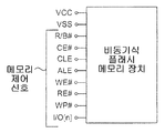
도 1b는 도 1a의 메모리 시스템에 이용될 수 있는 이산 플래시 메모리 장치(16-1∼16-4) 중 하나의 도면이다. 이러한 플래시 메모리 장치는 예를 들면 전원, 제어 포트 및 데이터 포트를 포함하는 여러 개의 입력 및 출력 포트를 포함한다. "포트"라는 용어는 메모리 장치로의 일반적인 입력 또는 출력 단자를 칭하는 것으로, 예를 들면 패키지 핀, 패키지 솔더 범프(solder bump), 칩 본드 패드, 및 무선 송신기 및 수신기를 포함한다. 전원 포트는 전력을 플래시 메모리 장치의 전체 회로에 공급하기 위한 VCC 및 VSS를 포함한다. 추가 전원 포트는 당업계에서 널리 알려진 것처럼 입력 및 출력 버퍼만을 공급하기 위하여 제공될 수 있다. 아래의 표 1은 제어 및 데이터 포트, 이에 대응하는 설명, 정의 및 예시적 로직 상태의 리스팅(listing)을 제공한다. 패키지 핀 및 볼 그리드 어레이는 포트의 물리적인 예로서, 패키징된 장치의 신호 또는 전압을 기판에 상호 연결하는 데 이용된다. 포트는 예를 들면 매립형 및 시스템-인-패키지(SIP) 시스템을 위한 단자 및 컨택트(contact)와 같은 다른 타입의 연결을 포함한다.FIG. 1B is a diagram of one of the discrete flash memory devices 16-1-16-4 that can be used in the memory system of FIG. 1A. Such flash memory devices include, for example, several input and output ports, including power supplies, control ports and data ports. The term "port" refers to a general input or output terminal to a memory device, and includes, for example, package pins, package solder bumps, chip bond pads, and wireless transmitters and receivers. The power supply port includes VCC and VSS for supplying power to the entire circuit of the flash memory device. Additional power ports may be provided to supply only input and output buffers as is well known in the art. Table 1 below provides a listing of the control and data ports and corresponding descriptions, definitions, and exemplary logic states. Package pins and ball grid arrays are used as physical examples of ports to interconnect signals or voltages of packaged devices to a substrate. Ports include other types of connections such as terminals and contacts, for example, for embedded and system-in-package (SIP) systems.
표 1에 나타낸 모든 신호들은 일반적으로 도 1b에 도시된 플래시 메모리 장치의 예의 동작에 대한 메모리 제어 신호로 칭한다. 플래시 메모리 장치에게 특정 동작을 실행하도록 지시하는 커맨드를 수신할 수 있으므로, 마지막 포트 I/O[n]은 메모리 제어 신호로서 간주됨에 주목하라. 포트 I/O[n]에 대해 어서트된(asserted) 커맨드는 I/O[n]을 구성하는 각각의 개별 신호 라인에 인가되는 로직 상태의 조합이므로, I/O[n]의 각각의 신호의 로직 상태는 예를 들면 WP#와 같은 다른 메모리 제어 신호 중 하나와 동일한 방식으로 기능한다. 주요 차이점은 기능을 수행하기 위해서 I/O[n] 로직 상태의 특정 조합이 플래시 메모리 장치를 제어한다는 점이다. 커맨드는 I/O 포트를 통해 수신되고, 커맨드 신호는 나머지 제어 포트를 포함한다. 당업자라면 동작 코드(op-코드)가 특정 메모리 동작을 실행하기 위한 커맨드내에 제공된다는 점을 이해할 것이다. 칩 인에이블 CE#을 제외하고, 모든 다른 포트는 채널(18)을 구성하는 각각의 글로벌 라인에 결합된다. 모든 포트는 메모리 동작을 실행하기 위하여 소정의 방법으로 제어된다. 어드레스, 커맨드 및 I/O 데이터는 I/O 포트에 제공되는 동안, 특정 제어 신호의 신호 타이밍 및 순서를 포함한다. 따라서, 도 1b의 비동기식 플래시 메모리 장치를 제어하기 위한 메모리 제어 신호는 특정 포맷 또는 프로토콜을 갖는다.All signals shown in Table 1 are generally referred to as memory control signals for the operation of the example flash memory device shown in FIG. 1B. Note that the last port I / O [n] is considered as a memory control signal because it can receive a command to instruct the flash memory device to perform a particular operation. Commands asserted for port I / O [n] are a combination of logic states applied to each individual signal line constituting I / O [n], so that each signal in I / O [n] The logic state of s functions in the same way as one of the other memory control signals, for example WP #. The main difference is that certain combinations of I / O [n] logic states control the flash memory device to perform the function. The command is received through the I / O port, and the command signal includes the remaining control port. Those skilled in the art will appreciate that the operation code (op-code) is provided in a command to perform a particular memory operation. Except for the chip enable CE #, all other ports are coupled to the respective global lines that make up the
도 1a의 비휘발성 메모리 장치 각각은 데이터를 수신하고 제공하기 위한 하나의 특정 데이터 인터페이스를 갖는다. 도 1a의 예에서, 이는 비동기식 플래시 메모리 장치에서 공통적으로 이용되는 병렬 데이터 인터페이스이다. 다중 비트의 데이터를 병렬로 제공하는 표준 병렬 데이터 인터페이스는 정격 동작 주파수를 넘어서 동작하는 경우에, 크로스토크(cross-talk), 신호 왜곡(signal skew) 및 신호 감쇄(signal attanuation)와 같은 신호 품질을 저하시키는 통신 품질 저하 효과의 문제점을 갖는 것으로 공지되어 있다.Each of the nonvolatile memory devices of FIG. 1A has one specific data interface for receiving and providing data. In the example of FIG. 1A, this is a parallel data interface commonly used in an asynchronous flash memory device. Standard parallel data interfaces that provide multiple bits of data in parallel provide signal qualities such as crosstalk, signal skew, and signal attanuation when operating beyond the rated operating frequency. It is known to have a problem of the effect of lowering the communication quality.
데이터 처리량을 증가시키기 위해서, 직렬 데이터 인터페이스를 갖는 메모리 장치가 공유된 미국 특허 공개 공보 제20070153576호 "출력 제어를 갖는 메모리", 및 공유된 미국 특허 공개 공보 제20070076502호 "데이지 체인 캐스캐이딩 장치"가 개시되어 있는데, 여기서는 예를 들면 200MHz의 주파수에서 직렬로 데이터를 수신하고 제공한다. 이는 직렬 데이터 인터페이스 포맷으로 칭한다. 이러한 공유된 특허 공개 공보에 제시된 것처럼, 설명된 메모리 장치는 서로에 대해 직렬로 연결된 메모리 장치의 시스템에 이용될 수 있다.In order to increase data throughput, a shared memory device having a serial data interface is disclosed in US Patent Publication No. 20070153576, "Memory with Output Control," and in US Patent Publication No. 20070076502, "Daisy Chain Cascading Device." Is disclosed herein, for example, receiving and providing data in series at a frequency of 200 MHz. This is called the serial data interface format. As set forth in this shared patent publication, the described memory devices can be used in a system of memory devices connected in series with each other.
도 2a는 직렬 메모리 시스템의 개념적 속성을 나타내는 블록도이다. 도 2a에서, 직렬 링-토폴로지(serial ring-topology) 메모리 시스템(20)은 출력 포트 세트(Sout) 및 입력 포트의 세트(Sin)를 갖는 메모리 제어기(22) 및 직렬로 연결된 메모리 장치(24, 26, 28 및 30)를 포함한다. 메모리 장치는 예를 들면 직렬 인터페이스 플래시 메모리 장치일 수 있다. 도 2a에는 도시되지 않았지만, 각각의 메모리 장치는 입력 포트 세트(Sin) 및 출력 포트 세트(Sout)를 갖는다. 이들 입력 및 출력 포트의 세트는 메모리 장치를 자신이 일부로서 속한 시스템에 인터페이스하는 물리적 핀이나 커넥션과 같은, 하나 이상의 개별 입/출력(I/O) 포트를 포함한다. 일 예에서, 메모리 장치는 플래시 메모리 장치일 수 있다. 이와 달리, 메모리 장치는 DRAM, SRAM, DiNOR 플래시 EEPROM, 직렬 플래시 EEPROM, Ferro RAM, Magneto RAM, 상 변화 RAM 또는 커맨드를 실행하기 위하여 또는 커맨드 및 데이터를 다음 메모리 장치로 통과시키기 위하여 특정 커맨드 구조와 호환하는 I/O 인터페이스를 갖는 임의의 다른 적절한 타입의 메모리 장치일 수 있다. 도 2a의 예에서는 4개의 메모리 장치를 포함하나, 다른 구성으로는 단일 메모리 장치 또는 적절한 수의 메모리 장치를 포함할 수 있다. 따라서, 메모리 장치(24)가 Sout에 연결된 것과 같이 시스템(20)의 제1 장치이면, 메모리 장치(30)는 Sin에 연결된 N번째 또는 마지막 장치일 수 있으며, 여기서 N은 0 보다 큰 정수이다. 메모리 장치(26 내지 28)는 제1과 마지막 메모리 장치 사이의 중간에 존재하는 직렬로 연결된 메모리 장치이다. 도 2a의 예에서, 메모리 장치(24 내지 30)는 동기식이며 서로에 대해 및 메모리 제어기(22)에 직렬로 연결된다.2A is a block diagram illustrating conceptual attributes of a serial memory system. In FIG. 2A, a serial ring-
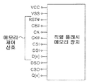
도 2b는 도 2a의 메모리 시스템에서 이용될 수 있는 직렬 인터페이스 플래시 메모리 장치(예를 들면, 24 내지 30)의 도면이다. 이 예에서 직렬 인터페이스 플래시 메모리 장치는 전원 포트, 제어 포트 및 데이터 포트를 포함한다. 전원 포트는 전력을 플래시 메모리 장치의 전체 회로에 공급하기 위한 VCC 및 VSS를 포함한다. 당해 분야에서 공지된 것처럼 입력 및 출력 버퍼만을 공급하기 위하여 추가의 전원 포트가 제공될 수 있다. 아래의 표 2는 제어 및 데이터 포트, 이에 대응하는 설명, 정의 및 예시적 로직 상태의 리스팅을 제공한다.FIG. 2B is a diagram of a serial interface flash memory device (eg, 24-30) that may be used in the memory system of FIG. 2A. In this example, the serial interface flash memory device includes a power port, a control port and a data port. The power supply port includes VCC and VSS for supplying power to the entire circuit of the flash memory device. Additional power ports may be provided to supply only input and output buffers as is known in the art. Table 2 below provides a listing of control and data ports and corresponding descriptions, definitions, and exemplary logic states.
신호 CSO, DSO 및 Q[n]은 예외로 하고, 표 2에 표시된 전체 신호는 도 2b에 도시된 플래시 메모리 장치의 예의 동작에 대한 메모리 제어 신호이다. CSO 및 DSO는 CSI 및 DSI의 재송신 버전이며, Q[n]은 커맨드 및 데이터를 제공하기 위한 출력이다. 커맨드은 D[n] 포트를 통해 수신되며, 커맨드 신호는 제어 포트 RST#, CE#, CK, CK#, CSI 및 DSI를 포함한다. 도 2a에 도시된 구성 예에서, 전체 신호는 메모리 제어기(22)로부터 직렬인 메모리 장치 각각에 직렬로 통과되고, 병렬로 전체 메모리 장치에 제공된 CE# 및 RST#는 예외로 한다. 도 2b의 직렬 인터페이스 플래시 메모리 장치는 그에 따라 메모리 동작을 실행하기 위하여 자신의 포맷 또는 프로토콜을 갖는 메모리 제어 신호를 수신한다.With the exception of the signals CSO, DSO and Q [n], the entire signal shown in Table 2 is a memory control signal for the operation of the example of the flash memory device shown in FIG. 2B. CSO and DSO are retransmission versions of CSI and DSI, and Q [n] is an output for providing commands and data. The command is received via the D [n] port and the command signals include control ports RST #, CE #, CK, CK #, CSI and DSI. In the example configuration shown in FIG. 2A, the entire signal is passed in series from the
도 2의 직렬 연결 메모리 시스템의 추가 상세가 2008년 2월 15일 출원된 "메모리 시스템에서의 클록 모드 결정"이란 명칭의 공유된 미국 특허 공개 공보 제20090039927호에 개시되며, 여기서는 각각의 메모리 장치가 병렬 클록 신호를 수신하는 직렬 메모리 시스템과 각각의 메모리 장치가 소스 동기식 클록 신호를 수신하는 직렬 메모리 시스템을 설명한다.Further details of the serially connected memory system of FIG. 2 are disclosed in shared US Patent Publication No. 20090039927, filed February 15, 2008, entitled “Clock Mode Determination in Memory Systems,” wherein each memory device is described. A serial memory system that receives parallel clock signals and a serial memory system where each memory device receives a source synchronous clock signal are described.
도 1b의 비동기식 플래시 메모리 장치와 도 2b의 직렬 인터페이스 메모리 장치의 양자를 공동 사용할 수 있으면, 메모리 시스템 제조자가 양 타입의 메모리 시스템을 제공할 수 있다. 그러나, 이는, 두 가지 상이한 타입의 메모리 장치가 공급되고 구매되어야 하므로, 메모리 시스템 제조자에게 높은 비용을 유발하기 쉽다. 당업자라면 대량으로 구매할 때 메모리 시스템의 비용을 최소화할 수 있으므로, 대량으로 구매할 때에 메모리 장치당 비용이 감소한다는 것을 이해할 것이다. 그러므로, 제조자가 양 타입의 메모리 시스템을 제공할 수 있지만, 나머지 한 타입에 대한 높은 시장 수요로 인해 하나의 타입의 메모리 장치에 대한 시장 수요가 떨어질 위험이 있다. 이러한 점 때문에 사용될 수 없는 메모리 장치의 공급에 대한 구매를 계속하도록 한다.If both the asynchronous flash memory device of FIG. 1B and the serial interface memory device of FIG. 2B can be used jointly, a memory system manufacturer can provide both types of memory systems. However, this is likely to incur high costs for memory system manufacturers because two different types of memory devices must be supplied and purchased. Those skilled in the art will appreciate that the cost per memory device is reduced when purchasing in large quantities, as the cost of the memory system can be minimized when purchasing in large quantities. Therefore, although a manufacturer can provide both types of memory systems, there is a risk that the market demand for one type of memory device will fall due to the high market demand for the other type. Because of this, the purchase of a supply of memory devices that cannot be used continues.
도 1b 및 도 2b에 도시된 것처럼, 비동기식 및 직렬 인터페이스 플래시 메모리 장치의 기능적 포트 할당 또는 정의가 서로와는 실질적으로 상이하며, 따라서 서로에 대해 호환 불가능이다. 이산 메모리 장치를 제어하는데 이용되는 신호 세트의 기능적 포트 정의 및 순서 또는 타이밍을 프로토콜 또는 포맷이라 한다. 그러므로, 비동기식 및 직렬 플래시 메모리 장치는 상이한 메모리 제어 신호 포맷에 응답하여 동작한다. 이는 도 2b의 직렬 인터페이스 플래시 메모리 장치가 멀티-드롭 메모리 시스템에 이용될 수 없으며, 따라서, 도 1b의 비동기식 플래시 메모리 장치가 직렬 연결된 링 토폴로지 메모리 시스템에 이용될 수 없음을 의미한다.As shown in Figures 1B and 2B, the functional port assignments or definitions of asynchronous and serial interface flash memory devices are substantially different from each other and are therefore incompatible with each other. The functional port definition and order or timing of a signal set used to control a discrete memory device is referred to as a protocol or format. Therefore, asynchronous and serial flash memory devices operate in response to different memory control signal formats. This means that the serial interface flash memory device of FIG. 2B cannot be used in a multi-drop memory system, and therefore, the asynchronous flash memory device of FIG. 1B cannot be used in a serially connected ring topology memory system.
도 1a 및 도 1b의 비동기식 플래시 메모리 장치에 걸쳐 개선된 성능을 위해서는 도 2a 및 도 2b에 도시된 것처럼 직렬 인터페이스 플래시 메모리 장치가 바람직하지만, 메모리 시스템 제조자는 비동기식 플래시 메모리 장치의 공급을 폐기하기를 바라지는 않을 것이다. 더욱이, 해당 산업에서의 이들의 유비쿼터스적 이용으로 인하여, 비동기식 플래시 메모리 장치는 도 2a의 직렬 인터페이스 플래시 메모리 장치와 같은 다른 플래시 메모리 장치에 비해 구매가 저렴하다. 현재, 메모리 시스템 제조자는 최소 비용 오버헤드로 직렬 상호 연결된 장치의 성능 이득을 취하는 해결책을 가지고 있지 않다.Serial interface flash memory devices are preferred as shown in FIGS. 2A and 2B for improved performance across the asynchronous flash memory devices of FIGS. 1A and 1B, but memory system manufacturers wish to discard the supply of asynchronous flash memory devices. Will not. Moreover, due to their ubiquitous use in the industry, asynchronous flash memory devices are less expensive to purchase than other flash memory devices such as the serial interface flash memory device of FIG. 2A. Currently, memory system manufacturers do not have a solution that takes the performance benefits of serially interconnected devices with minimal cost overhead.
여기서 설명된 적어도 일부의 실시예는 멀티-칩 패키지(MCP) 또는 시스템 인 패키지(SIP)에서 이산 메모리 장치와 함께 고속 인터페이스 칩 또는 브리지 장치를 갖는 복합 메모리 장치를 제공한다. 브리지 장치는 그 내부에 일체화되는 시스템과의 I/O 인터페이스를 제공하고, 글로벌 포맷에 따른 글로벌 메모리 제어 신호를 수신하고, 커맨드를 이산 메모리 장치와 호환하는 네이티브 또는 로컬 포맷을 따르는 로컬 메모리 제어 신호로 변환시킨다. 따라서 브리지 장치의 I/O 인터페이스에 의해 제공되는 성능 이득을 제공하면서, 브리지 장치는 NAND 플래시 장치와 같은 이산 메모리 장치의 재사용을 가능하게 한다. 브리지 장치는 패키지 내에 이산 메모리 장치 다이와 일체화된 이산 로직 다이로서 구현될 수 있다.At least some embodiments described herein provide a composite memory device having a high speed interface chip or bridge device along with a discrete memory device in a multi-chip package (MCP) or system in package (SIP). The bridge device provides an I / O interface with the system integrated therein, receives a global memory control signal in accordance with a global format, and directs the command to a local memory control signal that conforms to a native or local format compatible with a discrete memory device. Convert Thus, while providing the performance gain provided by the bridge device's I / O interface, the bridge device enables reuse of discrete memory devices such as NAND flash devices. The bridge device may be implemented as a discrete logic die integrated with a discrete memory device die in a package.
본 실시예에서, 글로벌 포맷은 도 2a 및 도 2b의 직렬 플래시 메모리 장치와 호환하는 직렬 데이터 포맷이며, 로컬 포맷은 도 1a 및 2b의 비동기식 플래시 메모리 장치와 호환하는 병렬 데이터 포맷이다. 그러나, 본 발명의 실시예는 상술한 포맷 예에 국한되지 않으며, 복합 메모리 장치에 이용되는 이산 메모리 장치의 타입 및 복합 메모리 장치가 그 내부에 이용되는 메모리 시스템의 타입에 따라, 임의의 메모리 제어 포맷 쌍도 사용될 수 있다. 예를 들면, 메모리 시스템의 글로벌 포맷은 Open NAND 플래시 인터페이스(ONFi) 표준을 따르고, 로컬 포맷은 비동기식 플래시 메모리 장치 메모리 제어 신호 포맷을 따를 수 있다. 예를 들면, 구체적으로 ONFi 표준은 ONFi 2.0 사양이다. 이와 달리, 글로벌 포맷은 비동기식 플래시 메모리 장치 메모리 제어 신호 포맷을 따르고, 로컬 포맷은 ONFi 2.0 사양 포맷을 따를 수 있다. 일반적으로, ONFi 사양은 데이터 및 커맨드가 클록과 동기하여 그 데이터 입/출력 포트를 통해 순응하는 메모리 장치에 제공되는 멀티-드롭(multi-drop) 동기 프로토콜이다. 바꿔 말하면, ONFi 순응 메모리 장치는, 하나의 중요한 차이점이 ONFi 순응 장치가 클록 신호를 수신하는 것인 병렬 양방향 입/출력 포트를 갖는 비동기 NAND 플래시 메모리 장치와 다소 유사성을 가질 수 있다.In this embodiment, the global format is a serial data format that is compatible with the serial flash memory devices of FIGS. 2A and 2B, and the local format is a parallel data format that is compatible with the asynchronous flash memory devices of FIGS. 1A and 2B. However, embodiments of the present invention are not limited to the above-described format examples, and may be any memory control format, depending on the type of discrete memory device used in the composite memory device and the type of memory system in which the composite memory device is used therein. Pairs may also be used. For example, the global format of the memory system may follow the Open NAND Flash Interface (ONFi) standard, and the local format may follow the asynchronous flash memory device memory control signal format. For example, specifically, the ONFi standard is the ONFi 2.0 specification. Alternatively, the global format may follow the asynchronous flash memory device memory control signal format, and the local format may follow the ONFi 2.0 specification format. In general, the ONFi specification is a multi-drop synchronization protocol in which data and commands are provided to memory devices that are synchronous with the clock and through their data input / output ports. In other words, an ONFi compliant memory device may have somewhat similarity to an asynchronous NAND flash memory device having a parallel bidirectional input / output port, where one important difference is that the ONFi compliant device receives clock signals.
도 3a는 본 실시예에 따른 복합 메모리 장치의 블록도이다. 도 3a에 도시된 바와 같이, 복합 메모리 장치(100)는 4개의 이산 메모리 장치(104)에 연결된 브리지 장치(102)를 포함한다. 이산 메모리 장치(104) 각각은 예를 들면 8Gb의 메모리 용량을 갖는 비동기식 플래시 메모리 장치일 수 있으나, 8Gb 장치 대신에 임의 용량의 이산 플래시 메모리 장치가 이용될 수 있다. 더욱이, 복합 메모리 장치(100)는 4개의 이산 메모리 장치를 갖는 것에 한정되지 않는다. 브리지 장치(102)가 복합 메모리 장치(100)에서 최대 수의 이산 메모리 장치를 수용하도록 설계되는 경우에는 임의의 적절한 수의 이산 메모리 장치가 포함될 수 있다.3A is a block diagram of a composite memory device according to the present embodiment. As shown in FIG. 3A, the
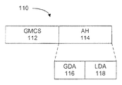
복합 메모리 장치(100)는 글로벌 커맨드를 수신하기 위한 입력 포트 GLBCMD_IN 및 수신된 글로벌 커맨드 및 판독 데이터를 통과시키기 위한 출력 포트 GLBCMD_OUT를 갖는다. 도 3b는 본 실시예에 따른 글로벌 커맨드의 계층 구조를 도시하는 개략도이다. 글로벌 커맨드(110)은 특정 포맷을 갖는 글로벌 메모리 제어 신호(GMCS)(112) 및 어드레스 헤더(AH)를 포함한다. 이러한 글로벌 메모리 제어 신호(112)는 도 2b의 직렬 인터페이스 플래시 메모리 장치를 위한 메모리 제어 신호와 같은 메모리 커맨드 및 커맨드 신호를 제공한다. 어드레스 헤더(114)는 시스템 레벨 및 복합 메모리 장치 레벨에서 이용되는 어드레싱 정보를 포함한다. 이러한 추가의 어드레싱 정보는 메모리 커맨드 내의 op-코드를 실행하기 위하여 복합 메모리 장치를 선택하기 위한 글로벌 장치 어드레스(GDA)(116) 및 op-코드를 실행하기 위한 선택된 복합 메모리 장치 내에서 특정 이산 장치를 선택하기 위한 로컬 장치 어드레스(LDA)(118)를 포함한다. 요약하면, 글로벌 커맨드는 하나의 포맷에 대응하는 전체 메모리 제어 신호를 포함하며, 또한 복합 메모리 장치 또는 그 안의 이산 메모리 장치를 선택하거나 제어하기 위하여 필요할 수도 있는 어드레싱 정보를 포함한다.The
브리지 장치(102)는 op-코드를 실행하지 않거나 또는 행 및 어드레스 정보를 갖는 임의의 메모리 위치에 액세스하지 않음에 주목한다. 브리지 장치(102)는 수신된 글로벌 메모리 제어 신호(112)를 변환하도록 선택되는지의 여부를 판정하기 위해 글로벌 장치 어드레스(116)를 사용한다. 선택되는 경우, 브리지 장치(102)는 다음으로 어떤 이산 메모리 장치에 변환된 글로벌 메모리 제어 신호(112)가 전송되는지를 판정하기 위하여 로컬 장치 어드레스(118)를 이용한다. 전체 4개의 이산 메모리 장치(104)와 통신하기 위하여, 브리지 장치(102)는 4개 세트의 로컬 I/O 포트(도시 생략)을 포함하며, 각각은 후술하는 바와 같이, 대응하는 이산 메모리 장치에 연결된다. 각각의 I/O 포트 세트는 적절한 동작을 위해 이산 메모리 장치가 필요로 하는 모든 신호를 포함하며, 이에 따라 로컬 장치 인터페이스로서 기능한다.Note that the
판독 데이터는 복합 메모리 장치(100)로부터 또는 이전의 복합 메모리 장치로부터 임의의 하나의 플래시 메모리 장치(104)에 의해 제공된다. 특히, 브리지 장치(102)는 메모리 시스템의 메모리 제어기에 연결되거나 또는 직렬 상호 연결된 장치의 시스템 내에서 다른 복합 메모리 장치의 다른 브리지 장치에 연결될 수 있다. 입력 포트 GLBCMD_IN 및 출력 포트 GLBCMD_OUT는 패키지 핀, 다른 물리적 도전체, 또는 복합 메모리 장치(100)로 및 로부터 글로벌 커맨드 신호 및 판독 데이터를 송/수신하기 위한 다른 임의의 회로일 수 있다. 브리지 장치(102)는 그에 따라, 도 2a의 메모리 제어기(22)와 같은 외부 제어기와 또는 시스템 내의 다른 복합 메모리 장치로부터의 브리지 장치와 통신이 가능하도록 하기 위하여 입력 포트 GLBCMD_IN 및 출력 포트 GLBCMD_OUT에 대응하는 연결을 가진다. 도 7의 실시예에 도시된 바와 같이, 많은 복합 메모리 장치가 서로 직렬로 연결될 수 있다.Read data is provided by any one
도 4는 실시예에 따른 브리지 장치(200)의 블록도로서, 도 3a에 도시된 브리지 장치(102)에 대응한다. 브리지 장치(200)는 브리지 장치 입력/출력 인터페이스(202), 메모리 장치 인터페이스(204), 및 포맷 변환기(206)를 갖는다. 포맷 변환기(206)는 제1 포맷인 글로벌 커맨드 및 글로벌 커맨드 신호를 포함하는 글로벌 메모리 제어 신호를 제2 포맷으로 변환하는 커맨드 포맷 변환기(208) 및 제1 포맷과 제2 포맷 사이에서 데이터를 변환하기 위한 데이터 포맷 변환기(210)를 포함한다. 커맨드 포맷 변환기(208)는 제1 포맷의 글로벌 메모리 제어 신호에 응답하여 도 3a의 이산 메모리 장치와 같은 이산 메모리 장치를 제2 포맷에 따라 제어하기 위한 상태 머신(도시 생략)을 더 포함한다.4 is a block diagram of a
브리지 장치 입력/출력 인터페이스(202)는 예를 들면 메모리 제어기 또는 다른 복합 메모리 장치와 같은 외부 장치와 통신한다. 브리지 장치 입력/출력 인터페이스(202)는 예를 들면 직렬 커맨드 포맷과 같은 글로벌 포맷의 다른 복합 메모리 장치 또는 메모리 제어기로부터 글로벌 커맨드를 수신한다. 도 3b를 참조하면, 입력/출력 인터페이스(202) 내의 로직은 글로벌 커맨드(110)가 대응하는 복합 메모리 장치에 어드레스되는지의 여부를 판정하기 위하여 글로벌 커맨드(110)의 글로벌 장치 어드레스(116)를 처리하고, 대응하는 복합 메모리 장치의 어떤 이산 메모리 장치가 op 코드 및 선택적인 행 및 열 어드레스 및 선택적인 기록 데이터를 포함하는 변환된 커맨드를 수신하는지의 여부를 판정하기 위하여 글로벌 커맨드(110)의 로컬 장치 어드레스(118)를 처리한다. 글로벌 커맨드가 브리지 장치(200)에 연결된 이산 메모리 장치에 어드레스되는 경우, 포맷 변환기(206) 내의 커맨드 포맷 변환기(208)는 op 코드 및 커맨드 신호 및 임의의 행 및 어드레스 정보를 제공하는 글로벌 메모리 제어 신호(112)를 글로벌 포맷에서 로컬 포맷으로 변환하고, 이를 메모리 장치 인터페이스(204)에 전달한다. 이 변환된 로컬 커맨드는 글로벌 포맷의 글로벌 신호에 기능이 대응하는 로컬 신호를 갖는다. 몇몇 경우에, 다중 로컬 커맨드가 글로벌 커맨드의 동작을 완료하는 데 필요할 수 있기 때문에, 다중 로컬 커맨드가 단일 글로벌 커맨드에 응답하여 발행될 수 있다. 기록 데이터가 예를 들면 직렬 데이터 포맷의 브리지 장치 입력/출력 인터페이스(202)에 제공되는 경우, 브리지 장치 입력/출력 인터페이스(202)는 병렬 포맷의 데이터 비트를 제공하기 위하여 직렬-병렬 변환 회로를 포함한다. 판독 동작을 위해, 브리지 장치 입력/출력 인터페이스(202)는 GLBCMD_OUT 출력 포트를 통한 출력을 위하여 직렬 포맷의 데이터 비트를 제공하기 위한 병렬-직렬 변환 회로를 포함한다.The bridge device input / output interface 202 is in communication with an external device such as, for example, a memory controller or other composite memory device. The bridge device input / output interface 202 receives global commands from another composite memory device or memory controller in a global format, such as, for example, a serial command format. Referring to FIG. 3B, logic in the input / output interface 202 processes the
커맨드 포맷 변환기(208)의 로직이 이산 메모리 장치(104)와 호환되도록 신호의 로직 변환을 실행하기 위하여 특별히 설계되므로, 글로벌 포맷 및 로컬 포맷은 공지된 것으로 간주된다. 커맨드 포맷 변환기(208)는, 네이티브 포맷을 갖는 메모리 제어기 신호로 이산 메모리 장치를 제어하는데 이용되는 메모리 시스템의 메모리 제어기의 것과 적어도 실질적으로 유사한 제어 로직을 포함할 수 있음에 주목한다. 예를 들면, 커맨드 포맷 변환기(208)는, 이산 메모리 장치가 메모리 장치(16-1 내지 16-4)와 같은 비동기식 메모리 장치라면, 도 1a의 메모리 제어기(14)의 동일한 제어 로직을 포함할 수 있다. 이는 커맨드 포맷 변환기(208)의 제어 로직이 이산 메모리 장치에 네이티브한 로컬 포맷의 메모리 제어 신호의 타이밍 및 순서를 제공한다는 것을 의미한다.Since the logic of the
글로벌 커맨드가 데이터 기록 동작에 대응하는 경우, 포맷 변환기(206)의 데이터 포맷 변환기(210)는 글로벌 포맷에서 로컬 포맷으로 데이터를 변환시키고, 이를 메모리 장치 인터페이스(204)에 전달한다. 판독 또는 기록 데이터의 비트는 로직 변환을 필요로 하지 않으며, 따라서 데이터 포맷 변환기(210)는 제1 데이터 포맷과 제2 데이터 포맷 사이의 데이터의 비트 위치에 대한 적절한 매핑을 보증한다. 포맷 변환기(206)는 이산 메모리 장치로부터의 판독된 데이터 또는 브리지 장치 입/출력 인터페이스(202)로부터 수신된 기록 데이터를 저장하기 위한 데이터 버퍼로서 기능한다. 그에 따라, 글로벌 포맷과 로컬 포맷 사이의 데이터 폭 불일치는 수용될 수 있다. 또한, 이산 메모리 장치와 브리지 장치(200) 사이 및 브리지 장치(200)와 다른 복합 메모리 장치 사이의 상이한 데이터 전송 속도는 데이터 포맷 변환기(210)의 버퍼링 기능으로 인하여 수용된다.When the global command corresponds to a data write operation, the
메모리 장치 인터페이스(204)는 그 후 로컬 커맨드 포맷의 변환된 커맨드를 도 3b의 글로벌 커맨드(110)의 로컬 장치 어드레스(118)에 의해 선택되는 이산 메모리 장치로 전달 또는 통신한다. 본 실시예에서, 변환된 커맨드는 커맨드 경로(212)를 통해 제공된다. 일 실시예에서, 커맨드 경로(212)는 복합 메모리 장치의 각각의 이산 메모리 장치와 메모리 장치 인터페이스(204) 사이에 연결된 i 세트의 전용 로컬 I/O 포트(LCCMD-i) 또는 채널을 포함한다. 변수 i는 복합 메모리 장치의 이산 메모리 장치의 수에 대응하는 정수이다. 예를 들면, 각각의 LCCMD-i 채널은 도 1b 및 표 1에 도시된 모든 포트를 포함한다. 대체 실시예에서, 예를 들면, LCCMD-i 채널은 커맨드 포맷 변환기(208)의 클록 회로에서 생성될 수 있는 클록 신호를 포함하는 ONFi 순응 장치의 전체 포트를 포함한다. 클록 생성 회로 및 기술은 당업계에 잘 알려져 있고, 본 실시예에서는, 클록 분주기 또는 체배기가 단일 "마스터" 클록 신호로부터 원하는 주파수를 갖는 클록 신호를 생성하도록 포함될 수 있다.The
이하는 도 3a의 복합 메모리 장치(100)를 더 참조로 하여 브리지 장치(200)의 동작 예를 설명한다. 판독 동작을 위하여, 입력 포트 GLBCMD_IN를 통하여 브리지 장치 입/출력 인터페이스(202)에 도달하는 글로벌 판독 커맨드와 같은 글로벌 커맨드가 수신된다. 이러한 글로벌 판독 커맨드는 브리지 장치(200)에 연결된 이산 메모리 장치(104)로부터 판독될 데이터에 대한 글로벌 포맷의 op 코드와 행 및 열 정보를 제공하는 글로벌 메모리 제어 신호를 포함한다. 브리지 장치 입/출력 인터페이스(202)가 글로벌 장치 어드레스(116)를 복합 메모리 장치(100)의 소정의 어드레스와 비교함으로써 글로벌 판독 커맨드에 대해 선택된 것으로 판정하는 경우, 커맨드 포맷 변환기(208)는 글로벌 판독 커맨드를 판독 데이터 커맨드가 실행되는 이산 메모리 장치(104)와 호환하는 로컬 포맷으로 변환한다. 후술하는 바와 같이, 복합 메모리 장치는 할당된 어드레스를 가질 수 있다. 글로벌 판독 커맨드의 로컬 장치 어드레스(118)는 메모리 장치 인터페이스(204)에 전달되고, 변환된 판독 데이터 커맨드는 커맨드 경로(212)의 로컬 I/O 포트의 대응하는 세트를 통해 로컬 장치 어드레스에 의해 어드레스되는 이산 메모리 장치에 제공된다.Hereinafter, an operation example of the
판독 데이터라고 칭하는 데이터는 선택된 이산 메모리 장치(104)로부터 판독되고, 로컬 포맷의 메모리 장치 인터페이스(204)의 동일한 로컬 I/O 포트를 통해 데이터 포맷 변환기(210)에 제공된다. 데이터 포맷 변환기(210)는 그 후 로컬 포맷으로부터 글로벌 포맷으로 판독 데이터를 변환하고, 판독 데이터를 선택된 이산 메모리 장치(104)로부터 브리지 장치 인터페이스(202)의 출력 포트 GLBCMD_OUT를 통해 메모리 제어기로 제공한다. 브리지 장치 인터페이스(202)는 데이터 포맷 변환기(210) 또는 입력 포트 GLBCMD_IN으로부터의 판독 데이터를 출력 포트 GLBCMD_OUT로 결합시키기 위한 내부 스위칭 회로를 포함한다.The data, referred to as read data, is read from the selected
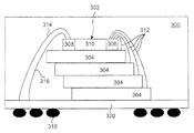
상술한 도 3a는 일 실시예에 따르는 복합 메모리 장치의 기능 표시이다. 도 5는 다른 실시예에 따르는 도 3a에 도시된 복합 메모리 장치에 대응하는 시스템 인 패키지(SIP)로서 제조된 복합 메모리 장치를 도시한다. 도 5는 패키지 내에 스택된 복합 메모리 장치의 단면을 도시한다. 패키지(300)는 도 3a의 브리지 장치(102)에 대응하는 브리지 장치(302), 및 또한 도 3a로부터의 이산 메모리 장치(104)에 각각 대응하는 4개의 이산 메모리 장치(304)를 포함한다. 본 실시예에서는, 이들 장치가 반도체 칩 또는 다이로 제조된다. 브리지 장치(302)는 예를 들면, 병렬 비동기 NAND 포맷과 같은 로컬 포맷으로 메모리 장치 인터페이스(306)를 통해 메모리 장치(304)와 통신한다. 브리지 장치(302)는 예를 들면, 앞서 설명한 직렬 데이터 포맷과 같은 글로벌 포맷으로 브리지 장치 입/출력 인터페이스(308)를 통해 다른 복합 메모리 장치의 브리지 장치와 또는 메모리 제어기(도시 생략)와 통신한다. 포맷 변환기(310)는 자신과 이산 메모리 장치(304) 사이의 단방향 커맨드 포맷 변환 및 양방향 데이터 포맷 변환을 제공하기 위해, 도 3a의 앞서 언급한 커맨드 포맷 변환기(208) 및 데이터 포맷 변환기(210)를 포함한다.3A is a functional representation of a composite memory device according to one embodiment. FIG. 5 illustrates a composite memory device manufactured as a system in package (SIP) corresponding to the composite memory device shown in FIG. 3A according to another embodiment. 5 shows a cross-section of a composite memory device stacked in a package. The
본 도시 예에서는, 복합 메모리 장치 패키지(300)는 SIP 시스템 또는 멀티-칩 패키지(MCP) 시스템이라고 한다. 패키지는 브리지 장치(302)와 모두 4개의 이산 메모리 장치(304)를 캡슐화한다. 배선(312)으로 표시된 로컬 통신 단말은 각 이산 메모리 장치(304)의 I/O 포트를 브리지 장치(302)의 메모리 장치 인터페이스(306)에 연결한다. 각 배선(312)은 로컬 포맷에 대응하는 모든 신호를 반송하는 하나의 채널 LCCMD-i를 나타낸다. 로컬 포맷의 일례는 표 1에 도시된 신호들을 포함하는 비동기 플래시 메모리 포맷이다. 배선(314 및 316)으로 표시된 글로벌 통신 단말은 입력 포트 GLBCMD_IN 및 출력 포트 GLBCMD_OUT를 각각 선택적 패키지 기판(320)을 통해 패키지 리드(318)에 연결한다. 서로에 관하여 브리지 장치(302)와 이산 메모리 장치(304)의 물리적인 배치는 브리지 장치(302)의 본드 패드의 위치 및 이산 메모리 장치(304)의 본드 패드의 위치에 의존한다.In the illustrated example, the composite
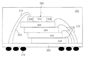
도 5a의 실시예에서, 각 이산 메모리 장치(304)는 브리지 장치(302)의 본드 패드에 직접 연결되는 자신의 데이터 본드 패드를 갖는다. 각 이산 메모리 장치(304)의 데이터 본드 패드는 브리지 장치(302)의 전용의 대응하는 데이터 본드 패드에 연결될 수 있는 채널을 형성한다. 도 5b에 도시된 대체 실시예에서는, 각 이산 메모리 장치(304)는 패키지 기판(320)에 형성된 도전성 트랙을 통해 브리지 장치(302)에 연결된다. 더욱 구체적으로는, 본드 배선(312)은 기판(320)에 형성되는 그러한 도전성 트랙을 통해 본드 배선(314)에 전기적으로 연결된다. 일 실시예에서, 각 이산 메모리 장치(304)는 도 5a의 실시예에서와 같은 각각의 채널을 통해 브리지 장치(302)의 대응하는 데이터 본드 패드에 전기적으로 연결된다. 이와 달리, 브리지 장치(302)는 각 이산 메모리 장치(304)의 데이터 본드 패드에 병렬로 연결되는 단지 한 세트의 데이터 본드 패드를 포함한다. 그에 따라, 모든 이산 메모리 장치(304) 사이에 공유되는 하나의 채널이 존재한다. 이 대체 실시예에서, 기판(320)에 형성되는 도전성 트랙은 브리지 장치(302)와 이산 메모리 장치(304)에 병렬로 결합될 수 있으며, 이것을 멀티-드롭 구성이라고 한다.In the embodiment of FIG. 5A, each
도 5a에 도시된 본 예에서, 이산 메모리 장치(304)는 위쪽 방향으로 향하는 자신의 본드 패드로 설치되고, 칩의 에지에 근접하게 위치하는 장치들의 본드 패드를 막지 않도록 노출을 위한 스태거된(staggered) 계단 패턴으로 서로 위에 스택된다. 브리지 장치(302)는 위쪽 방향으로 향하는 자신의 본드 패드로 설치되고, 스택의 최상위 이산 메모리 장치(304) 위에 스택된다. 이산 메모리 장치 본드 패드의 배치에 따라 다른 구성도 가능하고, 상이한 통신 단말이 본드 배선 대신에 사용될 수 있다. 예를 들면, 유도 결합 기술을 통한 무선 통신이 사용될 수 있거나, 관통 실리콘 비아(TSV: through silicon via) 상호 연결이 본드 배선 대신에 사용될 수 있다. "직렬 연결된 집적 회로를 스택하는 방법 및 그로부터 제작된 멀티-칩 장치"라는 명칭의 공유된 미국 특허 공개 공보 제20090020855호는 칩들을 함께 스택하기 위한 기술을 개시한다. 또한, 브리지 장치(302)는 패키지(300)에서의 스택의 크기에 크게 공헌하지 않는다. 따라서, 당업자에게는, 높은 저장 용량을 제공하면서, 복합 메모리 장치(300)가 더 큰 시스템에서 최소의 영역을 차지하는 것이 명확해야 한다.In this example shown in FIG. 5A, the
도 6은 인쇄 회로 기판(PCB) 상에 또는 모듈로서 형성된 도 3a의 복합 메모리 장치의 다른 실시예를 도시한다. 도 6에 도시된 바와 같이, 복합 메모리 장치(400)는 브리지 장치(402) 및 4개의 이산 메모리 장치(404)를 포함한다. 브리지 장치(402) 및 이산 메모리 장치(404)는 패키징된 장치이며, 이는 각각이 반도체 다이를 캡슐화하고 PCB 내에 미리 형성된 도전성 트랙에 본드되는 패키지 리드를 갖는 것을 의미한다. 브리지 장치(402)는 각 메모리 장치(404)에 대한 전용의 로컬 I/O 포트 또는 채널 LCCMD-i로서 구성되는 도전성 트랙을 통해 개별 이산 메모리 장치(404)에 연결된다. 브리지 장치를 포함하는 모듈 또는 PCB는 글로벌 커맨드를 수신하기 위한 입력 포트 GLBCMD_IN, 및 입력 포트에서 수신된 글로벌 커맨드와 판독 데이터를 제공하기 위한 출력 포트 GLBCMD_OUT를 포함한다. 이들 입력 및 출력 포트는 제어기(도시 생략) 또는 다른 복합 메모리 장치에 연결될 수 있다. 도 5a 및 5b의 실시예에 대해 설명한 바와 같이, 개별 이산 메모리 장치(404)는 각각 브리지 장치(402)에 직접 연결될 수 있거나, 이와 달리, 개별 메모리 장치(404)는 멀티-드롭 구성에서 브리지 장치(402)에 병렬로 연결될 수 있다.FIG. 6 illustrates another embodiment of the composite memory device of FIG. 3A formed on a printed circuit board (PCB) or as a module. As shown in FIG. 6, the
도 5a, 5b 및 도 6의 복합 메모리 장치 실시예는 다른 실시예에 따르는 도 2a의 직렬 메모리 시스템과 같은 메모리 시스템에서 이용될 수 있다. 그래서, 도 7의 메모리 시스템(500)은 도 2a의 직렬 메모리 시스템(20)과 유사하다. 메모리 시스템(500)은 메모리 제어기(502) 및 복합 메모리 장치(504-1 내지 504-j)를 포함하며, 여기서 j는 정수이다. 개별 복합 메모리 장치(504-1 내지 504-j)는 메모리 제어기(502)와 직렬로 상호 연결된다. 도 2a의 시스템(20)과 유사하게, 복합 메모리 장치(504-1)는 메모리 제어기(410)의 출력 포트(Sout)에 연결되어 있으므로 메모리 시스템(500)의 제1 복합 메모리 장치이며, 메모리 장치(504-n)는 메모리 제어기(410)의 입력 포트(Sin)에 연결되어 있으므로 마지막 장치이다. 복합 메모리 장치(504-2 내지 504-7)는 그 후 제1과 마지막 복합 메모리 장치 사이에 연결된 중간에 있는 직렬 연결 메모리 장치이다. Sout 포트는 글로벌 포맷의 글로벌 커맨드를 제공한다. Sin 포트는 글로벌 포맷의 판독 데이터 및 모든 복합 메모리 장치를 통해 전파하는 글로벌 커맨드를 수신한다.5A, 5B and 6 may be used in a memory system such as the serial memory system of FIG. 2A according to another embodiment. Thus, the
도 7에 도시된 복합 메모리 장치 각각은 도 3a에 도시된 복합 메모리 장치(100)와 유사하다. 복합 메모리 장치 각각은 브리지 장치(102) 및 4개의 이산 메모리 장치(104)를 갖는다. 전술한 바와 같이, 각각의 복합 메모리 장치에서의 각각의 브리지 장치(102)는 각각의 이산 메모리 장치(104)에 연결되고, 메모리 제어기(502) 및/또는 이전 또는 이후의 직렬-링 토폴로지 또는 직렬 상호 연결 구조의 복합 메모리 장치에 연결된다. 복합 메모리 장치(504-1 내지 504-j) 각각의 기능은 도 3a 및 도 4의 실시예에 대해 이전에 설명된 것과 동일하다.Each of the complex memory devices illustrated in FIG. 7 is similar to the
메모리 시스템(500)에서, 각각의 복합 메모리 장치는 고유의 글로벌 장치 어드레스가 할당된다. 이러한 고유의 글로벌 장치 어드레스는 브리지 장치(102)의 장치 어드레스 레지스터에 저장될 수 있으며, 보다 구체적으로는 도 4에 도시된 브리지 장치 블록도의 입/출력 인터페이스(202)의 레지스터에 저장될 수 있다. 이 어드레스는 "직렬 상호 결선의 혼합 장치 타입과 무관한 식별자 제조를 위한 장치 및 방법"이란 명칭의 공유인 미국 특허 공개 공보 제20080192649에 기재된 바와 같이, 장치 어드레스 할당 방식을 이용하여 메모리 시스템(500)의 작동 단계(power up phase) 동안 자동으로 할당될 수 있다. 또한, 각각의 복합 메모리 장치(504)는 각각의 복합 메모리 장치(504) 내의 이산 메모리 장치의 수에 대한 정보를 저장하기 위한 이산 장치 레지스터를 포함할 수 있다. 그러므로, 동작의 동일한 작동 단계 동안, 메모리 제어기는 각각의 이산 장치 레지스터를 쿼리(query)할 수 있고, 각각의 복합 메모리 장치내의 이산 메모리 장치의 수를 기록할 수 있다. 따라서, 메모리 제어기는 메모리 시스템(500)의 각각의 복합 메모리 장치(504)의 개별 이산 메모리 장치(104)를 선택적으로 어드레스할 수 있다.In
복합 메모리 장치(504-3)가 메모리 동작을 실행하기 위하여 선택되는 예를 이용한 메모리 시스템(500)의 동작은 이하와 같이 설명된다. 본 예에서, 메모리 시스템(500)은 도 2에 도시된 시스템과 유사한 직렬 연결된 메모리 시스템이며, 이산 메모리 장치(104)의 각각은 비동기식 NAND 플래시 메모리 장치로 상정한다. 그에 따라, 복합 메모리 장치(504-1 내지 504-j) 각각의 브리지 장치(102)는 메모리 제어기(502)에 의해 발행된 글로벌 포맷의 글로벌 커맨드를 수신하여 이들을 NAND 플래시 메모리 장치와 호환하는 로컬 포맷으로 변환하도록 설계된다. 또한, 메모리 시스템이 작동되고 각각의 복합 메모리 장치가 할당된 어드레스를 갖는 것으로 상정한다.The operation of the
메모리 제어기(502)는 Sout 포트로부터 복합 메모리 장치(504-3)에 대응하는 글로벌 장치 어드레스(116)를 포함하는 글로벌 커맨드를 발행한다. 제1 복합 메모리 장치(504-1)는 글로벌 커맨드를 수신하고, 그 브리지 장치(102)는 자신에 할당된 글로벌 장치 어드레스와 글로벌 커맨드 내의 어드레스를 비교한다. 글로벌 장치 어드레스가 불일치하므로, 복합 메모리 장치용의 브리지 장치(102)는 글로벌 커맨드를 무시하고, 글로벌 커맨드를 복합 메모리 장치(504-2)의 입력 포트로 통과시킨다. 자신에게 할당된 글로벌 장치 어드레스가 글로벌 커맨드 내의 어드레스와 불일치하므로, 복합 메모리 장치(504-2)에서는 동일한 동작이 발생한다. 따라서, 글로벌 커맨드는 복합 메모리 장치(504-3)로 통과된다.The
복합 메모리 장치(504-3)의 브리지 장치(102)는 자신에게 할당된 글로벌 장치 어드레스와 글로벌 커맨드 내의 어드레스 사이의 일치를 판정한다. 그에 따라, 복합 메모리 장치(504-3)의 브리지 장치(102)는 글로벌 메모리 제어 신호를 NAND 플래시 메모리 장치와 호환하는 로컬 포맷으로 변환하게 된다. 브리지 장치는 그 후 변환된 커맨드를 글로벌 커맨드 내에 포함되는 로컬 장치 어드레스(118)에 의해 선택된 NAND 플래시 메모리 장치에 전송한다. 선택된 NAND 플래시 장치는 그 후 수신된 로컬 메모리 제어 신호에 대응하는 동작을 실행한다.The
복합 메모리 장치(504-3)의 브리지 장치(102)가 글로벌 커맨드를 변환하는 동안, 글로벌 커맨드를 다음 복합 메모리 장치로 통과시킨다. 나머지 복합 메모리 장치는 글로벌 커맨드를 무시하고, 글로벌 커맨드는 결국 메모리 제어기(502)의 Sin 포트에서 수신된다. 글로벌 커맨드가 판독 동작에 대응하는 경우, 복합 메모리 장치(504-3)의 선택된 NAND 플래시 메모리 장치는 판독 데이터를 로컬 포맷으로 대응하는 브리지 장치(102)에 제공한다. 브리지 장치(102)는 그 후 판독 데이터를 로컬 포맷으로 변환하여, 이를 그 출력 포트를 통해 다음 복합 메모리 장치로 통과시킨다. 나머지 복합 메모리 장치 전체의 브리지 장치(102)는 판독 데이터를 메모리 제어기(502)의 Sin 포트로 통과시킨다. 당업자라면 NAND 플래시 메모리 장치에서의 상이한 동작을 실행하기 위하여 다른 글로벌 커맨드가 발행될 수 있고, 그 전체가 선택된 복합 메모리 장치(102)의 브리지 장치(102)에 의해 변환될 수 있음을 이해할 것이다.While the
본 실시예에서, 글로벌 커맨드는 메모리 시스템(500) 내의 전체 복합 메모리 장치에 전파된다. 다른 실시예에 따르면, 브리지 장치(102)는 메모리 시스템(500) 내의 추가의 복합 메모리 장치에 글로벌 커맨드가 전파되는 것을 억제하기 위한 추가의 로직을 포함한다. 더욱 상세하게는, 글로벌 장치가 자신에게 어드레스된다고 선택된 복합 메모리 장치가 판정한 경우, 대응하는 브리지 장치(102)는 그 출력 포트를 예를 들면, VSS 또는 VDD의 고정 전압 값과 같은 널(null) 값으로 구동한다. 그에 따라, 나머지 비선택된 복합 메모리 장치는 이들이 글로벌 커맨드를 실행하지 않으므로 스위칭 전력을 보존한다. 그러한 직렬 연결된 메모리 시스템에 대한 절전 방법이 "직렬 상호 결선된 혼합 장치 타입과 무관한 식별자의 제조 장치 및 방법"이라는 명칭의 공유된 미국 특허 공개 공보 제20080201588호에 기재되어 있으며, 그 내용은 전부 참고로 본 명세서에 통합되어 있다.In this embodiment, the global command is propagated to the entire composite memory device in the
전술한 도 7의 실시예는 동일한 타입의 예를 들면, 비동기식 NAND 플래시 메모리 장치와 같은 이산 메모리 장치를 갖는 각각의 복합 메모리 장치(504-1 내지 304-N)를 구비하는 메모리 시스템을 도시한다. 이는 모든 복합 메모리 장치가 동일하기 때문에 균질 메모리 시스템으로 칭한다. 대체 실시예에서는, 상이한 복합 메모리 장치가 상이한 타입의 이산 메모리 장치를 갖는, 비균질 메모리 시스템이 가능하다. 예를 들면, 일부 복합 메모리 장치가 비동기식 NAND 플래시 메모리 장치를 포함하는 한편, 다른 것들은 NOR 플래시 메모리 장치를 포함할 수 있다. 그러한 대체 실시예에서, 전체 복합 메모리 장치는 동일한 글로벌 포맷을 따르지만, 내부적으로는 각각의 복합 메모리 장치는 글로벌 포맷 메모리 제어 신호를 NOR 플래시 메모리 장치 또는 NAND 플래시 메모리 장치에 대응하는 로컬 포맷 메모리 제어 신호로 변환하도록 설계되는 브리지 장치(200)를 갖는다.The foregoing embodiment of FIG. 7 illustrates a memory system having each composite memory device 504-1 through 304-N having the same type of discrete memory device, such as, for example, an asynchronous NAND flash memory device. This is called a homogeneous memory system because all composite memory devices are identical. In alternative embodiments, heterogeneous memory systems are possible, where different composite memory devices have different types of discrete memory devices. For example, some composite memory devices may include asynchronous NAND flash memory devices, while others may include NOR flash memory devices. In such an alternative embodiment, the entire composite memory device follows the same global format, but internally each composite memory device converts the global format memory control signal into a NOR flash memory device or a local format memory control signal corresponding to the NAND flash memory device. It has a
또 다른 실시예에서, 단일 복합 메모리 장치는 상이한 타입의 이산 메모리 장치를 가질 수 있다. 예를 들면, 단일 복합 메모리 장치는 2개의 비동기식 NAND 플래시 메모리 장치 및 2개의 NOR 플래시 메모리 장치를 포함할 수 있다. 이러한 "혼합된" 또는 "비균질" 복합 메모리 장치는 전술한 동일한 글로벌 포맷을 따르지만, 내부적으로는 그 브리지 장치는 글로벌 포맷 메모리 제어 신호를 NAND 플래시 메모리 장치 및 NOR 플래시 메모리 장치에 대응하는 로컬 포맷 메모리 제어 신호로 변환하도록 설계될 수 있다.In yet another embodiment, a single composite memory device may have different types of discrete memory devices. For example, a single composite memory device may include two asynchronous NAND flash memory devices and two NOR flash memory devices. Such "mixed" or "homogeneous" composite memory devices follow the same global format described above, but internally the bridge device sends global format memory control signals to local format memory control corresponding to NAND flash memory devices and NOR flash memory devices. It can be designed to convert to a signal.
그러한 브리지 장치는 NAND 플래시 메모리 장치와 NOR 플래시 메모리 장치 각각에 대한 하나의 전용 포맷 변환기를 포함할 수 있으며, 이는 글로벌 커맨드 내에 제공되는 전술한 어드레스 정보에 의해 선택될 수 있다. 도 3b에 대해 설명한 바와 같이, 어드레스 헤더(114)는 시스템 레벨 및 복합 메모리 장치 레벨에서 사용되는 어드레싱 정보를 포함한다. 이러한 추가의 어드레싱 정보는 메모리 커맨드 내의 op 코드를 실행하도록 복합 메모리 장치를 선택하기 위한 글로벌 장치 어드레스(GDA)(116) 및 op 코드를 실행하도록 선택된 복합 메모리 장치 내에서 특정 이산 장치를 선택하기 위한 로컬 장치 어드레스(LDA)(118)를 포함한다. 브리지 장치는 2개의 포맷 변환기 중 어떤 것으로 글로벌 커맨드가 라우팅되는지를 판정하기 위하여 LDA(118)를 사용하는 선택기를 가질 수 있다.Such a bridge device may include one dedicated format converter for each of the NAND flash memory device and the NOR flash memory device, which may be selected by the above-mentioned address information provided in the global command. As described with respect to FIG. 3B, the
메모리 시스템(500)의 대체 실시예에서는, 복합 메모리 장치는 도 1a에 도시된 멀티 드롭 메모리 시스템과 같은 멀티 드롭 구성의 메모리 시스템에서 사용될 수 있다. 이 실시예에서는, 도 1a의 채널(18)과 같은 단일 채널을 통해 메모리 제어기 및 서로에 병렬로 연결된다. 따라서, 각 복합 메모리 장치의 브리지 장치는 동일한 데이터 입/출력 포트를 통해 판독 데이터를 제공하면서, 도 1b의 데이터 입/출력 포트 I/O[n]과 같은 데이터 입/출력 포트를 통해 커맨드 및 데이터를 수신하도록 구성된다. 일례에서, 각 복합 메모리 장치의 브리지 장치는 비동기식 제어 신호 또는 동기식 제어 신호를 수신하도록 구성된다. 비동기식 제어 신호에 대해, 메모리 제어기는 각 복합 메모리 장치의 브리지 장치에 의해 수신되는 소스 동기식 클록 신호를 제공한다. 본 실시예의 일례에서는, 브리지 장치는 브리지 장치에 의해 이산 메모리 장치와 호환되는 포맷으로 변환될 수 있는 ONFi 표준 커맨드를 수신하도록 구성된다.In alternative embodiments of the
이산 메모리 장치와 관련되는 복합 메모리 장치의 전체 판독 및 기록 성능을 향상시키기 위해, 브리지 장치는 이산 메모리 장치의 최대 정격 주파수보다 더 큰 주파수에서 판독 데이터를 제공하고 기록 데이터를 수신하도록 구성된다. 그러나, 복합 메모리 장치 내에서 사용하기 위해 선택된 이산 메모리 장치에 따라서는, 그들 이산 메모리 장치는, 브리지 장치가 더 높은 데이터 속도로 판독 데이터를 출력할 수 있게 하기 위해 실시간으로 브리지 장치에 충분히 빠른 자신의 판독 데이터를 제공할 수 없을 수도 있다. 유사하게, 기록 데이터가 고속으로 브리지 장치에 제공될 수 있지만, 이산 메모리 장치는 매우 느린 기록 속도를 가질 수도 있다. 그에 따라, 이 속도의 불일치를 보상하기 위해, 브리지 장치는 이산 메모리 장치의 페이지 버퍼로부터 판독되거나, 이산 메모리 장치의 페이지 버퍼에 기록될 데이터의 페이지의 적어도 일부를 일시적으로 저장하기 위한 가상 페이지 버퍼를 포함한다. 본 실시예에 따르면, 이들 가상 페이지 버퍼는 이산 메모리 장치로부터의 판독 데이터 또는 이산 메모리 장치에 기록될 기록 데이터를 저장하는 메모리를 포함한다. 예를 들어, 도 4의 실시예에서는, 데이터 포맷 변환기(210)는 예컨대, SRAM 또는 DRAM 메모리와 같은 공지된 메모리일 수 있는 그런 메모리를 포함한다. 가상 페이지 버퍼의 더욱 상세한 설명은 도 8에 도시된 실시예를 참조하여 기술한다.In order to improve the overall read and write performance of the composite memory device associated with the discrete memory device, the bridge device is configured to provide read data and receive write data at a frequency greater than the maximum rated frequency of the discrete memory device. However, depending on the discrete memory devices selected for use within the composite memory device, those discrete memory devices may be fast enough for the bridge device in real time to allow the bridge device to output read data at a higher data rate. It may not be possible to provide read data. Similarly, although write data can be provided to the bridge device at high speed, the discrete memory device may have a very slow write speed. Accordingly, to compensate for this discrepancy in speed, the bridge device may include a virtual page buffer for temporarily storing at least a portion of the page of data to be read from the page buffer of the discrete memory device or written to the page buffer of the discrete memory device. Include. According to this embodiment, these virtual page buffers include a memory for storing read data from the discrete memory device or write data to be written to the discrete memory device. For example, in the embodiment of FIG. 4,
도 8은 4개의 NAND 플래시 메모리 장치의 페이지 버퍼와 브리지 장치의 메모리 사이의 관계를 도시하는 복합 메모리 장치(600)의 블록도이다. 복합 메모리 장치(600)는 도 3a에 도시된 복합 메모리 장치(100)와 유사하며, 도 8의 실시예에서는 4개의 NAND 플래시 메모리 장치(602) 및 브리지 장치(604)를 포함한다. 브리지 장치(604)는 도 4의 브리지 장치(400)를 간략하게 한 버전으로 도시되며, 메모리(606)만이 도시된다. 브리지 장치의 다른 부품은 도 8에서는 생략되지만, 브리지 장치(600)의 적절한 동작을 보장하기 위해서는 존재하는 것으로 이해되어야 할 것이다. 후술하는 바와 같이, 메모리(606)는 4개의 NAND 플래시 메모리 장치(602) 각각의 페이지 버퍼와 대응하는 그룹으로 논리적으로 구성된다.8 is a block diagram of a
각각의 NAND 플래시 메모리 장치(602)는 각각이 "플레인 0" 및 "플레인 1"로 라벨 붙여진 2개의 플레인(608 및 610)으로 구성된 메모리 어레이를 갖는다. 도시되지는 않았지만, 행 회로는 플레인(608 및 610) 각각을 통해 수평으로 연장하는 워드라인을 구동하며, 열 액세스 및 센스 회로를 포함할 수 있는 페이지 버퍼(612 및 614)는 플레인(608 및 610) 각각을 통해 수직으로 연장하는 비트라인에 연결된다. 이러한 회로의 목적 및 기능은 당업자에게는 널리 알려져 있다. 임의의 판독 또는 기록 동작에 있어서, 하나의 논리 워드라인은 플레인(608 및 610) 모두에 걸쳐 구동되고, 하나의 행 어드레스가 플레인(608 및 610) 모두에서 동일한 물리적 워드라인을 구동하는 것을 의미한다. 판독 동작에서, 선택된 논리 워드라인에 연결된 메모리 셀내에 저장된 데이터가 감지되어 페이지 버퍼(612 및 614) 내에 저장된다. 유사하게, 기록 데이터는 선택된 논리 워드라인에 연결된 메모리 셀에 프로그래밍하기 위하여 페이지 버퍼(612 및 614) 내에 저장된다.Each NAND
브리지 장치(604)의 메모리(606)는 각각이 적어도 동일한 저장 용량의 페이지 버퍼(612 또는 614)를 갖는 논리적 또는 물리적 서브 메모리(616)로 분할된다. 논리적 서브 메모리는 메모리의 물리 블록 내의 할당된 어드레스 공간일 수 있으며, 물리적 서브 메모리는 고정된 어드레스 공간을 갖는 구별되게 형성된 메모리이다. 서브 메모리(616)는 Bank 0 내지 Bank 3으로 라벨 붙여진 메모리 뱅크(618)로 그룹화되며, 여기에서 메모리 뱅크(618)의 서브 메모리(616)는 하나의 NAND 플래시 메모리 장치(602)의 페이지 버퍼와만 관련된다. 다시 말하면, 메모리 뱅크(618)의 서브 메모리(616)는 하나의 NAND 플래시 메모리 장치(602)의 각각의 페이지 버퍼(612 및 614)에 전용이다. 판독 동작 동안, 페이지 버퍼(612 및 614) 내의 판독 데이터는 대응하는 메모리 뱅크(618)의 서브 메모리(616)로 전송된다. 프로그램 동작 동안, 메모리 뱅크(618)의 서브 메모리(616) 내에 저장된 기록 데이터는 대응하는 NAND 플래시 메모리 장치(602)의 페이지 버퍼(612 및 614)로 전송된다. NAND 플래시 메모리 장치(602)는 단일 플레인 또는 2 보다 많은 플레인을 가질 수 있으며, 각각이 대응하는 페이지 버퍼를 갖는다. 그에 따라, 메모리(606)는 각각의 페이지 버퍼에 전용인 서브 메모리를 갖도록 대응하여 구성될 것이다.The
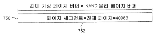
도 8에 따른 본 예는 페이지 버퍼 공간이 총 8KB이고, 2개의 개별 4KB 페이지 버퍼로서 구성된 NAND 플래시 장치(602)를 갖는다. 각각의 개별 4KB 페이지 버퍼는 예를 들면 플레인(608) 또는 플레인(610)과 같은 각각의 플레인의 비트라인에 결합된다. 당업자라면 페이지 버퍼 크기는 NAND 플래시 메모리 장치의 전체 용량이 증가함에 따라 서서히 증가해서, 향후 NAND 플래시 메모리 장치는 실질적으로 훨씬 큰 페이지 버퍼를 가질 것임을 이해할 것이다. NAND 플래시 메모리 장치의 코어 판독 및 프로그램 시간은 대체로 일정하고, 당업자에게는 공지된 페이지 버퍼 크기와는 무관하므로, 큰 페이지 버퍼는 고속의 전체 판독 및 프로그램 동작을 고려한 것이다. 크기가 절반인 페이지 버퍼와 비교할 때, 다른 코어 판독 동작이 메모리 어레이의 상이한 행 내에 저장된 다른 데이터의 페이지에 액세스하는데 필요하기 전에, 큰 페이지 버퍼는 2배의 판독 데이터의 상대적으로 상수인 버스트 판독을 가능하게 한다. 유사하게, 2배의 기록 데이터는 다른 기록 데이터의 페이지가 페이지 버퍼 내에 로딩될 필요가 있기 전에, 동시에 메모리 어레이에 프로그램될 수 있다. 그에 따라, 큰 페이지 버퍼는 음악 또는 비디오 데이터가 크기면에서 여러 페이지일 수 있는 멀티미디어 애플리케이션용으로 적합하다.This example according to FIG. 8 has a
도 8의 복합 메모리 장치(600)에서, 총 코어 판독 시간은 앞에서 Tr이라고 한 NAND 플래시 메모리 장치 코어 판독 시간과 전송 시간(Ttr)의 합을 포함한다. 전송 시간(Ttr)은 페이지 버퍼(612 및 614)의 콘텐츠를 출력 또는 판독하기 위한 NAND 플래시 메모리 장치에 필요한 시간이어서, 이들은 하나의 메모리 뱅크(618)의 대응하는 서브 메모리(616)에 기록될 수 있다. 총 코어 프로그램 시간은 프로그램 전송 시간(Ttp)과 앞서 Tpgm이라고 한 NAND 플래시 메모리 장치 코어 프로그램 시간의 합을 포함한다. 프로그램 전송 시간(Ttp)은 하나의 메모리 뱅크(618)의 서브 메모리(616)의 콘텐츠를 출력 또는 판독하기 위하여 브리지 장치(608)에 필요한 시간이어서 이들은 프로그래밍 동작 이전에 NAND 플래시 메모리 장치(602)의 대응하는 페이지 버퍼(612 및 614)로 로딩될 수 있다. 멀티미디어 애플리케이션에 있어서, 데이터는 상이한 NAND 플래시 메모리 장치에 걸쳐 저장될 수 있고, 하나의 NAND 플래시 메모리 장치의 코어 동작을 마스크하도록 동시에 동작될 수 있는 한편, 다른 NAND 플래시 메모리 장치(602)에 대응하는 데이터는 브리지 장치(604)에 의해 출력된다. 예를 들면, 하나의 메모리 뱅크(618)로부터의 데이터의 버스트 판독 동안, 코어 판독 동작은 다른 메모리 뱅크(618)의 서브 메모리(616)를 다른 NAND 플래시 메모리 장치(602)로부터의 데이터로 로딩하기 위해 이미 진행중일 수 있다.In the
파일 크기가 NAND 플래시 메모리 장치 페이지 버퍼의 전체 페이지 크기보다 작은 애플리케이션이 있을 수 있다. 그러한 파일은 퍼스널 컴퓨터 데스크탑 애플리케이션에 일반적으로 이용되는 텍스트 파일 및 다른 유사한 타입의 데이터 파일을 포함한다. 사용자는 일반적으로 그러한 파일을 NAND 플래시 메모리를 공통으로 사용하는 USB 비휘발성 저장 드라이브에 복사한다. 다른 부상하는 애플리케이션은 자기 하드 디스크 드라이브(HDD)를 대체할 수 있는 고체 드라이브(SSD)로서, 데이터를 저장하기 위하여 NAND 플래시 메모리 또는 다른 비휘발성 메모리를 사용한다. 복합 메모리 장치 판독 및 프로그램 순서는 아래의 차이점을 제외하고는 전술한 것과 동일하다. 이 예에서, 원하는 데이터는 전체 페이지 크기보다 작으며, 다른 데이터를 갖는 페이지 내에 저장된다고 상정한다. 판독 동작에 있어서, 전체 페이지 버퍼 데이터가 선택된 NAND 플래시 메모리 장치(602)의 페이지 버퍼(612 및 614)로부터 대응하는 서브 메모리(616)로 전송된 이후에, 열 어드레스가 메모리 뱅크(618)의 서브 메모리(616) 내에 저장된 원하는 데이터의 최초 및 최후 비트 위치의 장소를 한정하는데 이용된다. 데이터의 최초, 최후 및 중간 비트만이 브리지 장치(604)의 서브 메모리(616)로부터 판독된다.There may be applications where the file size is smaller than the total page size of the NAND flash memory device page buffer. Such files include text files and other similar types of data files commonly used in personal computer desktop applications. Users typically copy such files to USB nonvolatile storage drives that commonly use NAND flash memory. Another emerging application is a solid state drive (SSD) that can replace a magnetic hard disk drive (HDD), which uses NAND flash memory or other nonvolatile memory to store data. The compound memory device read and program order is the same as described above except for the following differences. In this example, it is assumed that the desired data is smaller than the total page size and stored in a page with other data. In a read operation, after the entire page buffer data is transferred from the page buffers 612 and 614 of the selected NAND
그러한 시나리오에서의 전송 시간(Ttr)은 복합 메모리 장치의 전체 코어 판독 시간에 대한 현저한 기여로 인하여 특정 애플리케이션에 대해서는 허용되지 않는다. 그러한 애플리케이션은 판독 동작이 가능한 신속히 수행되어야 하는 경우의 SSD를 포함한다. NAND 플래시 메모리 장치에 대한 코어 판독 시간(Tr)이 임의으 페이지 버퍼 크기에 대해 일정하게 유지되며, 전체 콘텐츠를 서브 메모리(616)로 전송하기 위한 전송 시간(Ttr)은 페이지 버퍼 크기에 직접적으로 의존한다.The transfer time Ttr in such a scenario is not allowed for certain applications due to the significant contribution to the total core read time of the composite memory device. Such applications include SSDs where read operations should be performed as quickly as possible. The core read time (Tr) for the NAND flash memory device remains constant for any page buffer size, and the transfer time (Ttr) for transferring the entire content to the
본 실시예에 따르면, 복합 메모리 장치 내의 NAND 플래시 메모리 장치의 페이지 버퍼의 최대 물리적 크기보다 작은 가상 페이지 크기라고 칭하는 가상의 최대 페이지 크기를 가지도록 메모리 뱅크(618)의 서브 메모리(616)를 구성함으로써 복합 메모리 장치의 전송 시간(Ttr)은 최소화될 수 있다. 특정 메모리 뱅크(618)에 대한 가상 페이지 크기 설정을 기초로 하여, 페이지 버퍼 내에 저장된 가상 페이지 크기에 대응하는 데이터의 세그먼트만이 대응하는 서브 메모리(616)에 전송되는 경우에, 브리지 장치(604)는 판독 명령을 발행한다. 페이지 버퍼의 이러한 세그먼트는 페이지 세그먼트라고 한다.According to the present embodiment, by configuring the
도 9a 내지 9c는 본 실시예에 따라서 플래시 메모리 장치와 같은 이산 메모리 장치로부터 판독되는 한 세트의 가상 페이지 크기에 대응하는 데이터가 어떻게 복합 메모리 장치로부터 판독되는지를 설명한다. 도 9a 내지 9c는 하나의 완전히 도시된 제1 NAND 플래시 메모리 장치(702), 제2 NAND 플래시 메모리 장치(704)의 일부, 브리지 장치(706)의 일부를 갖는 복합 메모리 장치(700)를 도시한다. 이 예에서의 NAND 플래시 메모리 장치는 단일 페이지 버퍼(710)에 연결된 비트라인을 갖는 단일 플레인(708)을 갖는다. 브리지 장치(706)의 도시된 부분은 제1 서브 메모리(712), 제2 서브 메모리(714) 및 브리지 장치 입력/출력 인터페이스(716)를 포함한다. 제1 서브 메모리(712)는 제1 NAND 플래시 메모리 장치(702)와 관련된 제1 뱅크에 대응하는 한편, 제2 서브 메모리(714)는 제2 NAND 플래시 메모리 장치(704)와 관련된 제2 뱅크에 대응한다. 본 실시예에서 판독 동작을 설명하는 것을 목적으로, NAND 플래시 메모리 장치(702)로부터의 데이터가 액세스되고, 제1 뱅크(제1 서브 메모리(712))의 가상 페이지 크기는 페이지 버퍼(710)의 최대 물리적 크기보다 작게 되도록 설정되는 것을 상정한다.9A to 9C illustrate how data corresponding to a set of virtual page sizes read from a discrete memory device such as a flash memory device is read from the composite memory device according to this embodiment. 9A-9C show a
도 9a에서 시작하여, 브리지 장치(706)가 제1 NAND 플래시 메모리 장치(702) 내에 저장된 데이터에 액세스하기 위한 판독 동작을 나타내는 글로벌 메모리 제어 신호를 수신하였고, 적절한 로컬 메모리 제어 신호를 제1 NAND 플래시 메모리 장치(702)로 인코드하여 제공하였음을 가정한다. 판독 명령에 대응하는 로컬 메모리 제어 신호에 응답하여, 제1 NAND 플래시 메모리 장치(702)는 로컬 메모리 제어 신호내의 어드레스 정보에 의해 선택된 행 또는 워드라인(718)을 활성화한다. 도 9b로 진행하여, 워드라인(718)이 활성화되는 경우 또는 이에 연결된 메모리 셀의 저장된 데이터에 액세스하는데 유효한 전압 레벨까지 구동되는 경우, 각각의 액세스된 메모리 셀에 연결된 비트라인 상에서 생성된 전류 또는 전압은 페이지 버퍼(710) 내부의 감지 회로에 의해 감지된다. 그러므로, 액세스된 메모리 셀의 데이터 상태는 페이지 버퍼(710) 내에 저장된다. 도 9c에서, NAND 플래시 메모리 장치(702)는 페이지 버퍼(710)의 비트 위치의 특정 범위 내에 저장된 데이터를 브리지 장치(706) 특히 제1 서브 메모리(712)에 출력한다. 이러한 데이터 출력 공정은 NAND 플래시 메모리 장치(702)에 대한 최대 정격 속도 또는 데이터 속도까지 실행된다.Beginning in FIG. 9A, the
NAND 플래시 메모리 장치(702)의 예에서, 선택된 행(718)으로부터의 판독된 데이터가 일반적으로 대기/비지(ready/busy) 신호에 의해 페이지 버퍼(710) 내에 저장되는 것을 NAND 플래시 메모리 장치(702)가 브리지 장치(706)에 보고 또는 신호하면, 비트 위치의 특정 범위에 대응하는 열 어드레스를 포함하는 버스트 판독 명령이 자동으로 브리지 장치(706)에 의해 제공된다. 열 어드레스는 제1 서브 메모리(712)에 대해 설정된 가상 페이지 크기를 기초로 하여 결정된다. 제1 서브 메모리(712) 내에 저장된 데이터는 그 후 고속 또는 데이터 속도로 브리지 장치 입/출력 인터페이스(716)를 경유하여 복합 메모리 장치(700)의 출력 데이터 포트를 통해 출력된다. 본 실시예에서는, 출력 데이터 포트는 표 2에 앞서 도시된 Q[n] 데이터 출력 포트에 대응하는 핀 또는 리드를 포함한다.In the example of NAND
그에 따라, 제1 서브 메모리(712)에 대한 가상 페이지 크기를 페이지 버퍼(710)의 최대 물리적 크기보다 작게 설정함으로써, 페이지 버퍼(710)로부터의 데이터의 대응하는 크기의 페이지 세그먼트만이 제1 서브 메모리(712)로 출력된다는 것을 알 수 있다. 이러한 페이지 세그먼트는 각각이 열 어드레스에 의해 어드레스 가능한 비트 위치의 특정 범위를 포함한다. 후술하는 바와 같이, 페이지 세그먼트는 어드레스 가능하다. 따라서, NAND 플래시 메모리 장치(702)가 페이지 버퍼(710)로부터 데이터의 이러한 페이지 세그먼트를 출력하기 위한 전송 시간(Ttr)은 페이지 버퍼(710)의 전체 데이터가 제1 서브 메모리(712)에 전송되는 상황과 관련하여 현저히 감소될 수 있다.Accordingly, by setting the virtual page size for the
상술한 예는 어떻게 전송 시간(Ttr)이 최소화될 수 있는지를 설명한다. 가상 페이지 크기가 페이지 버퍼(710)의 최대 물리적 크기보다 작아지도록 설정하면 기록 동작 동안 동일한 성능 이점을 제공한다. 기록 동작에서, 도 9a 내지 9c에 도시된 순서는 유효하게 반대가 된다. 예를 들면, 기록 데이터는 브리지 장치 입/출력 인터페이스(716)에 의해 수신되고, 제1 서브 메모리(712)와 같은 서브 메모리에 기록된다. 이러한 기록 데이터는 미리 설정된 가상 페이지 크기에 일치하는 크기를 가지며, 이는 페이지 버퍼(710)로 전송된다. 이러한 기록 데이터를 브리지 장치(706)로부터 페이지 버퍼(710)에 전송하는데 필요한 시간은 전송 시간(Ttr)으로서, 기록 데이터의 크기 및 NAND 플래시 메모리 장치(702)의 동작 주파수에 의존한다. 기록 데이터는 페이지 세그먼트라고 하는 페이지 버퍼(710)의 특정 비트 위치 내에 저장되며, NAND 플래시 메모리(702)의 코어 프로그래밍 동작은 선택된 행(718)의 활성화 및 페이지 버퍼(710) 내에 저장된 기록 데이터에 응답하여 필요한 프로그래밍 전압을 비트라인에 인가하는 것을 통해 시작된다. 그에 따라, 기록 동작 동안 전송 시간(Ttr)을 단축함으로써, 메모리 시스템의 전체 기록 시간이 감소된다.The above example illustrates how the transmission time Ttr can be minimized. Setting the virtual page size to be smaller than the maximum physical size of the
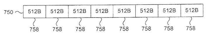
본 실시예에 따르면, 브리지 장치(706)의 제1 서브 메모리(712)는 미리 설정된 가상 페이지 크기 중 어느 하나를 갖도록 인식된 커맨드를 통해 구성될 수 있다. 제1 서브 메모리(712)의 가상 페이지 크기가 설정되면, 대응하는 NAND 플래시 메모리 장치의 페이지 버퍼(710)는 설정된 가상 페이지 크기에 대응하는 동일한 크기의 페이지 세그먼트로 논리적으로 분할된다. 도 10a 내지 10d는 설정된 가상 페이지 크기를 기초로 상이한 크기의 페이지 세그먼트를 갖는 NAND 플래시 메모리 장치 페이지 버퍼(750)를 개략적으로 도시한다. 페이지 세그먼트는 페이지 버퍼(750) 내의 가상 어드레스 공간을 나타낸다. 도 10a 내지 10d에 따른 본 실시예에서, NAND 플래시 페이지 버퍼 및 브리지 장치의 서브 메모리의 양자는 최대 4K의 물리적 크기를 갖는다. 도 10a에서, 가상 페이지 크기(VPS)는 최대 또는 최고 4K 크기로 설정되어서, 단 하나의 페이지 세그먼트(752)만이 존재한다. 도 10b에서, VPS는 2K로 설정되어, 2개의 2K 페이지 세그먼트(754)가 된다. 도 10c에서, VPS는 1K로 설정되고, 4개의 1K 페이지 세그먼트(756)가 된다. 도 10d에서, VPS는 612 바이트(B)로 설정되어, 크기가 612B인 8페이지 세그먼트(758)가 된다. 당업자라면 더 소형 크기의 VPS가 가능하고, 대응하는 페이지 세그먼트가 가능하다는 것과, 페이지 세그먼트의 총 수는 NAND 플래시 메모리 장치 페이지 버퍼(750)의 최대 크기에 의존하는 것을 이해할 것이다.According to the present embodiment, the
본 실시예에 대해 전술한 바와 같이, NAND 플래시 메모리 장치의 페이지 버퍼(750)가 판독 동작에 대한 데이터로 로딩된 이후에, 페이지 버퍼(750)의 페이지 세그먼트만이 브리지 장치로 출력된다. 원하는 데이터는 페이지 버퍼(750)의 특정 페이지 세그먼트 중 하나에 저장될 수 있다. 그러므로, 각각의 페이지 세그먼트는 글로벌 명령내에 제공된 가상 페이지 어드레스에 의해 브리지 장치로 어드레스 가능하다. 예를 들면, 2개의 어드레스 비트는 도 10c의 4개의 페이지 세그먼트(756) 중 하나를 선택하는데 이용된다. 선택된 경우에, 원하는 데이터는 페이지 버퍼(750)의 선택된 페이지 세그먼트 내의 전체 비트 위치를 점유하지 않을 수 있다. 그러므로, 가상 열 어드레스는 판독 데이터가 일반적으로는 버스트 판독 동작에서 판독 데이터가 판독되는 선택된 페이지 세그먼트 내에서 제1 비트 위치를 선택하는데 이용된다. 표 3은 이하에서 도 10a 내지 10d에 도시된 예를 든 페이지 세그먼트를 기초로 한 예시된 어드레싱 방식을 요약한다.As described above for this embodiment, after the
예시적 어드레싱 방식이 예를 들면 표 3에 도시되어 있지만, 당업자라면 상이한 어드레싱 방식이 NANA 플래시 메모리 장치의 페이지 버퍼의 크기에 의존하여 이용될 수 있음을 이해할 것이다. 표 3에 도시된 바와 같이, 각각의 어드레싱 방식은 2 이상의 페이지 세그먼트를 어드레스하기 위한 제1 수의 비트 및 선택된 페이지 세그먼트 내의 열을 어드레스하기 위한 제2 수의 비트를 포함한다. 제1 수의 비트는 가상 페이지 어드레스(VPA)라고 하고, 제2 수의 비트는 가상 열 어드레스(VCA)라고 한다. 가상 페이지 어드레스 및 가상 열 어드레스는 총체적으로 간략히 가상 어드레스라고 한다. 본 실시예에서, 각각의 서브 메모리 또는 서브 메모리의 뱅크의 VPS 설정은 판독 데이터를 요청하는 메모리 제어기 또는 다른 호스트 시스템에 알려지며, 기록 데이터를 복합 메모리 장치에 제공한다. 그에 따라, NAND 플래시 메모리 장치의 페이지 버퍼로부터 페이지 세그먼트를 판독하기 위한 가상 어드레스는 글로벌 명령 내에 특정 NAND 플래시 메모리 장치에 액세스하기 위하여 대응하는 어드레싱 방식으로 복합 메모리 장치에 제공된다. 표 3에 도시된 것을 포함하는 가능한 어드레싱 방식은 페이지 버퍼의 가상 또는 논리적 어드레스 공간을 어드레스한다. 이러한 논리적 어드레스 공간이 도 10a 내지 10d의 페이지 버퍼(750)내의 페이지 세그먼트의 비트 위치로서 기술되었지만, 실제 페이지 버퍼는 실제 물리적 어드레스들로 어드레스된다. 논리 어드레스의 물리 어드레스로의 매핑은 당업계에 잘 알려져 있다.Although an example addressing scheme is shown in Table 3, for example, those skilled in the art will appreciate that different addressing schemes may be used depending on the size of the page buffer of the NANA flash memory device. As shown in Table 3, each addressing scheme includes a first number of bits for addressing two or more page segments and a second number of bits for addressing a column in the selected page segment. The first number of bits is called a virtual page address (VPA) and the second number of bits is called a virtual column address (VCA). Virtual page addresses and virtual column addresses are collectively referred to simply as virtual addresses. In this embodiment, the VPS setting of each sub memory or bank of sub memories is known to a memory controller or other host system requesting read data, and provides write data to the composite memory device. Accordingly, a virtual address for reading page segments from the page buffer of the NAND flash memory device is provided to the composite memory device in a corresponding addressing manner to access a particular NAND flash memory device within a global command. Possible addressing schemes, including those shown in Table 3, address the virtual or logical address space of the page buffer. Although this logical address space is described as the bit position of the page segment in the
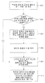
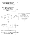
이하, 본 발명의 실시예에 따라서, 이산 메모리 장치로부터 데이터를 판독하고 이산 메모리 장치에 데이터를 기록하는 방법을 논의한다. 도 11은 본 실시예에 따르는 복합 메모리 장치로부터 데이터를 판독하는 방법을 개략적으로 나타낸 플로우차트인 한편, 도 12는 복합 메모리 장치에 데이터를 기록하는 방법을 개략적으로 나타낸 플로우차트이다.Hereinafter, in accordance with an embodiment of the present invention, a method of reading data from and writing data to a discrete memory device is discussed. FIG. 11 is a flowchart schematically showing a method of reading data from the composite memory device according to the present embodiment, while FIG. 12 is a flowchart schematically showing a method of writing data to the composite memory device.
지금 설명하는 도 11의 방법에서는, 복합 메모리 장치의 하나의 특정 이산 메모리 장치가 그로부터 데이터를 판독하기 위해 선택되는 것으로 상정한다. 또한, 선택된 이산 메모리 장치는 특정의 가상 페이지 사이즈 구성을 갖도록 구성되어 있다고 상정한다. 그 방법은 단계 800에서 시작하며, 여기에서 브리지 장치는 선택된 이산 메모리 장치의 물리 페이지(PP)로부터 특정 가상 페이지(VP)에서 데이터를 판독하도록 글로벌 페이지 판독 커맨드를 수신한다. 본 예에서는, PP=A 및 VP=X이며, 여기에서 A는 메모리의 페이지의 물리 어드레스를 나타내고, X는 모든 가상 페이지 중 물리 페이지를 생성하는 특정 가상 페이지를 나타낸다. 브리지 장치는 글로벌 판독 커맨드를 로컬 판독 커맨드로 변환하여, 그것을 선택된 이산 메모리 장치에 발행한다. 이산 메모리 장치는 PP=A에서 로컬 페이지 판독 커맨드를 수신하여, 내부 코어 판독 동작을 시작한다. 단계 802에서, 현재의 판독 동작이 새로운 PP로 향하면, 방법은 단계 804로 진행한다. 단계 804에서, 브리지 장치는 자신의 가상 페이지 버퍼를 클리어하며, 이 단계는 그들의 모든 상태를 로직 "1" 또는 "0" 레벨로 설정하는 단계를 포함할 수 있다. 단계 806에서, 브리지 장치는 그 후 PP=A에서 자신의 페이지 버퍼에 데이터를 로드하도록 이산 메모리 장치에 특정된 내부 코어 판독 시간 Tr동안 대기한다. 코어 판독 시간 Tr이 경과하면 단계 808로 진행하여, 브리지 장치는 이산 메모리 장치에 로컬 버스트 데이터 판독 커맨드를 발행한다. 응답 시에, 이산 메모리 장치는 단계 808에서 브리지 장치에 VP=X에 대응하는 열 어드레스 범위에 저장되는 데이터를 출력하고, 브리지 장치는 이 데이터를 자신의 가상 페이지 버퍼에 저장한다. 단계 808에서, 브리지 장치는 가상 페이지 버퍼에 저장된 데이터가 이제 독출될 수 있다는 것을 호스트 시스템이나 메모리 제어기에 나타내기 위해 READY 플래그를 설정한다.In the method of FIG. 11 now described, assume that one particular discrete memory device of a composite memory device is selected to read data therefrom. It is also assumed that the selected discrete memory device is configured to have a specific virtual page size configuration. The method begins at
단계 802로 되돌아가서, 현재의 판독 동작이 이전의 판독 동작의 동일한 PP로 향하면, 즉, PP=A이면, 방법은 브리지 장치가 버스트 데이터 판독 커맨드를 이산 메모리 장치에 발행하는 단계 808로 스킵(skip)한다. 응답 시에, 이산 메모리 장치는 VP=Y를 출력한다. 예를 들면, 이 후속하는 판독 동작이 PP=A 및 VP=Y에대한 것이면, 여기에서 Y는 X와 상이한 특정의 가상 페이지를 나타내며, 자신의 페이지 버퍼가 이미 P=A의 전체 데이터 내용을 저장하기 때문에 이산 메모리 장치 코어 판독 동작은 불필요하며, 전체 데이터 내용은 VP=X와 VP=Y의 양자에 대응하는 데이터를 포함한다. 이 상황에서, 이산 메모리 장치는, 단계 808에서 브리지 장치에 의해 자신이 가상 페이지 버퍼에 수신되어 저장되는, VP=Y에 대응하는 열 어드레스 범위에 저장된 데이터를 출력하는 것만 필요하다. 설정된 READY 플래그에 응답하여, 메모리 제어기는 가상 페이지 버퍼에 저장된 데이터를 출력하도록 글로벌 버스트 데이터 판독 커맨드를 발행할 수 있다.Returning to step 802, if the current read operation is directed to the same PP of the previous read operation, ie PP = A, the method skips to step 808 where the bridge device issues a burst data read command to the discrete memory device. )do. In response, the discrete memory device outputs VP = Y. For example, if this subsequent read operation is for PP = A and VP = Y, then Y represents a specific virtual page that is different from X, and its page buffer already stores the entire data content of P = A. Therefore, the discrete memory device core read operation is unnecessary, and the entire data content includes data corresponding to both VP = X and VP = Y. In this situation, the discrete memory device only needs to output the data stored in the column address range corresponding to VP = Y, which is received and stored in the virtual page buffer by the bridge device in
전술한 판독 방법 실시예에서, PP=A로부터 VP=X 및 VP=Y의 판독이 순서대로 일어난다. 특히, 단계 800 내지 810은 복합 메모리 장치로부터 VP=X를 독출하기 위해 실행되고, VP=Y를 판독하기 위해 단계 800, 802, 808 및 810만을 수반하는 다른 판독 동작이 뒤따른다. 도 11에 도시된 판독 방법의 대체 실시예에 따르면, VP=Y에대한 제2 페이지 판독 커맨드가 제1 버스트 데이터 판독 커맨드에 앞서 발행될 수 있다. 이 방법으로, 이산 메모리 장치와 브리지 칩 사이에서의 VP=Y에 대응하는 데이터의 전송이 VP=X에 대응하는 데이터가 브리지 장치로부터 출력되는 것과 동시에 일어날 수 있다.In the above-described reading method embodiment, reading of VP = X and VP = Y from PP = A takes place in order. In particular, steps 800 to 810 are executed to read VP = X from the composite memory device, followed by other read operations involving only steps 800, 802, 808, and 810 to read VP = Y. According to an alternative embodiment of the read method shown in FIG. 11, a second page read command for VP = Y may be issued prior to the first burst data read command. In this way, the transfer of data corresponding to VP = Y between the discrete memory device and the bridge chip may occur simultaneously with the data corresponding to VP = X being output from the bridge device.
본 실시예에 따르는 복합 메모리 장치에 데이터를 기록하는 방법을 이하 설명한다. 도 12의 방법에서는, 복합 메모리 장치의 하나의 특정 이산 메모리 장치가 자체에 데이터를 기록하기 위해 선택되는 것으로 상정한다. 또한 이산 메모리 장치가 특정의 가상 페이지 크기 구성을 갖도록 구성되었다고 상정한다. 프로그래밍 방법은 단계 900에서 개시하며, 여기에서 글로벌 페이지 프로그램 커맨드가 브리지 장치에 의해 수신된다. 이 예에서는, 데이터가 PP=A로 기록되고, 데이터는 VP=X에 대응한다. 단계 900에서 페이지 프로그램 커맨드의 수신 시에, 브리지 장치의 가상 페이지 버퍼는 프로그래밍될 데이터(VP=X)가 로드된다. 단계 902에서, 브리지 장치는 버스트 데이터 로드 개시 커맨드를 이산 메모리 장치에 발행한 후 VP=X를 이산 메모리 장치에 전송한다. 이어서 단계 904에서, PP=A의 다른 가상 페이지에 대응하는 데이터가 기록되면, 방법은 단계 906으로 진행하여, 여기에서 브리지 장치가 다른 버스트 데이터 로드 커맨드를 이산 메모리 장치에 발행한다. 이 커맨드는 VP=Y와 같은 다른 가상 페이지에 대응하는 데이터를 이산 메모리 장치에 전송한다. 단계 906으로부터, 방법은 단계 904로 루프 백(loops back)한다.A method of writing data in the composite memory device according to the present embodiment will be described below. In the method of FIG. 12, it is assumed that one particular discrete memory device of the composite memory device is selected to write data to itself. It is also assumed that the discrete memory device is configured to have a specific virtual page size configuration. The programming method begins at
PP=A 내에 프로그램될 추가의 가상 페이지가 없는 경우, 방법은 단계 908로 진행하며, 여기에서 브리지 장치가 프로그램 커맨드를 이산 메모리 장치에 발행한다. 이것이 이산 메모리 장치의 VP=X 및/또는 VP=Y 내지 PP=A와 같은 데이터를 프로그램하기 위해 이산 메모리 장치 내에서 코어 프로그래밍 동작을 시작한다. 이어서 단계 910에서, 브리지 장치는 통과하기 위한 코어 프로그래밍 시간 Tprog을 대기한 후, READY 플래그를 설정하며, 이 플래그는 메모리 제어기에 VP=X 및 VP=Y 내지 PP=A에 대한 프로그램 동작이 완료된 것을 나타낸다.If there are no additional virtual pages to be programmed in PP = A, the method proceeds to step 908, where the bridge device issues a program command to the discrete memory device. This initiates a core programming operation within the discrete memory device to program data such as VP = X and / or VP = Y to PP = A of the discrete memory device. Subsequently, in
전술한 복합 메모리 장치의 실시예는 하나의 포맷의 메모리 제어 신호에 응답하여 이산 메모리 장치가 제2 및 상이한 포맷을 갖는 글로벌 메모리 제어 신호를 이용하여 어떻게 제어될 수 있는지를 나타낸다. 대체 실시예에 따르면, 브리지 장치(200)는 동일한 포맷을 갖는 로컬 메모리 제어 신호를 이산 메모리 장치에 제공하기 위해 하나의 포맷을 갖는 글로벌 메모리 제어 신호를 수신하도록 설계될 수 있다. 바꿔 말하면, 그러한 복합 메모리 장치는 이산 메모리 장치를 제어하기 위해 이용되는 메모리 제어 신호를 수신하도록 구성된다. 그러한 구성은 복수의 이산 메모리 장치가 복합 메모리 장치 내의 다른 이산 메모리 장치와 무관하게 동작하는 메모리 뱅크로서 각각 기능하도록 할 수 있다. 그에 따라, 각 이산 메모리 장치는 브리지 장치(200)로부터 커맨드를 수신하여, 대체로 서로 병렬로 동작을 실행하게 된다. 이것은 또한 동시 발생 동작이라고 칭한다. 브리지 장치(200)의 설계는 그에 따라 커맨드 변환 회로가 불필요하기 때문에 간략화된다.The above-described embodiment of the composite memory device illustrates how a discrete memory device can be controlled using a global memory control signal having a second and different format in response to a memory control signal of one format. According to an alternative embodiment, the
전술한 실시예는 복합 메모리 장치 내의 이산 메모리 장치가 어떻게 외국의 커맨드 포맷에 응답할 수 있는지를 설명한다. 이것은 수신된 글로벌 커맨드를 이산 메모리 장치와 호환되는 네이티브 커맨드 포맷으로 변환하는 브리지 장치를 통해 달성된다. 예로서, 직렬 커맨드 포맷은 비동기식 NAND 플래시 포맷으로 변환될 수 있다. 실시예는, 임의의 쌍의 커맨드 포맷이 한쪽에서 다른 쪽으로 변환될 수 있기 때문에, 이들 2개의 포맷에 한정되지 않는다.The above-described embodiment describes how the discrete memory device in the composite memory device can respond to a foreign command format. This is accomplished through a bridge device that converts the received global command into a native command format compatible with the discrete memory device. As an example, the serial command format may be converted to an asynchronous NAND flash format. Embodiments are not limited to these two formats, since any pair of command formats can be converted from one side to the other.
이상의 설명에서는, 설명을 위한 목적으로, 본 발명의 실시예의 전체적인 이해를 제공하기 위해 다수의 상세 설명이 제시된다. 그러나, 당업자에게는 이들 특정 상세 설명이 발명을 실시하기 위해 필요하지 않다는 것이 명백하다. 다른 예에서는, 발명을 이해하기 쉽게 하기 위해 잘 알려진 전기 구조체 및 회로가 블록도 형태로 도시되어 있다.In the foregoing description, for purposes of explanation, numerous specific details are set forth in order to provide a thorough understanding of embodiments of the present invention. However, it will be apparent to one skilled in the art that these specific details are not required in order to practice the invention. In other instances, well-known electrical structures and circuits are shown in block diagram form in order to facilitate understanding of the invention.
본 명세서에서 하나의 소자가 다른 소자에 "연결" 또는 "결합"되어 있다고 할 때, 그것이 다른 소자에 직접 연결 또는 결합될 수 있거나 개재하는 소자가 존재할 수 있는 것을 이해할 것이다. 대비하여, 본 명세서에서 하나의 소자가 다른 소자에 "직접 연결" 또는 "직접 결합"되어 있다고 할 때, 개재하는 소자는 없다. 소자들 사이의 관계를 설명하기 위해 사용된 다른 단어는 유사한 방식으로 해석되어야 한다(즉, "사이"와 "바로 그 사이", "인접한"과 "바로 인접한", 등).When one device is referred to herein as being "connected" or "coupled" to another device, it will be understood that it may be directly connected or coupled to or intervened with another device. In contrast, when one device is "directly connected" or "directly coupled" to another device in the present specification, there is no intervening device. Other words used to describe the relationship between elements should be interpreted in a similar manner (ie, "between" and "just between", "adjacent" and "immediately adjacent", etc.).
이 출원의 도면들은 일정한 비율로 할 필요는 없다. 예를 들면, 도 5에서, 브리지 장치(302) 및 이산 메모리 장치(304)의 상대 크기는 일정한 비율로 하지 않고, 제작된 브리지 장치는 이산 메모리 장치(304)보다 면적이 한자릿수 작다.The drawings in this application are not necessarily to scale. For example, in FIG. 5, the relative size of the
설명한 실시예의 어떤 각색 및 변형이 이루어질 수 있다. 그에 따라, 상기 논의된 실시예들은 예시적이며 한정하지 않는다고 상정한다.Any adaptation and modification of the described embodiments can be made. Accordingly, it is assumed that the embodiments discussed above are exemplary and not limiting.
Claims (71)
제2 포맷을 갖는 글로벌 메모리 제어 신호를 수신하여 상기 글로벌 메모리 제어 신호를 상기 로컬 메모리 제어 신호로 변환하는 브리지 장치를
포함하는, 복합 메모리 장치.At least one discrete memory device that executes a memory operation in response to a local memory control signal having a first format, and
A bridge device for receiving a global memory control signal having a second format and converting the global memory control signal into the local memory control signal;
And a composite memory device.
상기 적어도 하나의 이산 메모리 장치에 연결되는 로컬 입/출력 포트,
상기 글로벌 메모리 제어 신호를 수신하는 글로벌 입력 포트, 및
상기 글로벌 메모리 제어 신호와 상기 적어도 하나의 이산 메모리 장치로부터의 판독 데이터 중 하나를 제공하는 글로벌 출력 포트를
포함하는, 복합 메모리 장치.The method according to claim 1, wherein the bridge device,
A local input / output port coupled to the at least one discrete memory device,
A global input port for receiving the global memory control signal, and
A global output port providing one of the global memory control signal and read data from the at least one discrete memory device
And a composite memory device.
메모리 동작에 대응하는 글로벌 커맨드를 제공하는 메모리 제어기; 및
링 토폴로지 구성으로 상기 메모리 제어기 및 서로와 직렬로 연결되는 n개의 복합 메모리 장치를 포함하며, 상기 n개의 복합 메모리 장치의 각각은 m개의 이산 메모리 장치 및 브리지 장치를 갖고, 상기 n개의 복합 메모리 장치 중 선택된 복합 메모리 장치의 상기 브리지 장치는 상기 m개의 이산 메모리 장치 중 선택된 이산 메모리 장치에 대한 메모리 동작에 대응하는 로컬 메모리 제어 신호를 제공하기 위해 상기 글로벌 커맨드를 수신하며, 여기에서 n 및 m은 0보다 큰 정수인, 메모리 시스템.As a memory system,
A memory controller providing a global command corresponding to a memory operation; And
A ring topology configuration comprising the memory controller and n composite memory devices connected in series with each other, wherein each of the n composite memory devices has m discrete memory devices and a bridge device, and among the n composite memory devices The bridge device of the selected composite memory device receives the global command to provide a local memory control signal corresponding to a memory operation for the selected discrete memory device of the m discrete memory devices, where n and m are greater than zero. A memory system that is a large integer.
상기 글로벌 커맨드를 수신하는 입력 포트 및 상기 글로벌 커맨드를 제공하는 출력 포트를 갖는 브리지 장치 입/출력 인터페이스 - 상기 브리지 장치는 상기 글로벌 장치 어드레스를 글로벌 장치 어드레스 레지스터에 저장된 소정의 어드레스와 비교함 - ;
상기 글로벌 장치 어드레스가 상기 소정의 어드레스와 일치할 때, 상기 글로벌 커맨드의 상기 글로벌 메모리 제어 신호를 제1 포맷으로부터 제2 포맷을 갖는 상기 로컬 메모리 제어 신호로 변환하는 포맷 변환 회로; 및
상기 로컬 장치 어드레스에 응답하여 상기 로컬 메모리 제어 신호를 상기 선택된 이산 메모리 장치에 제공하는 메모리 장치 인터페이스를
포함하는, 메모리 시스템.The method according to claim 19, The bridge device,
A bridge device input / output interface having an input port for receiving the global command and an output port for providing the global command, the bridge device comparing the global device address with a predetermined address stored in a global device address register;
A format conversion circuit for converting the global memory control signal of the global command from the first format to the local memory control signal having a second format when the global device address matches the predetermined address; And
A memory device interface for providing the local memory control signal to the selected discrete memory device in response to the local device address;
Which includes, a memory system.
상기 제1 포맷의 상기 글로벌 메모리 제어 신호를 상기 제2 포맷을 갖는 상기 로컬 메모리 제어 신호로 변환하는 커맨드 포맷 변환기; 및
상기 선택된 이산 메모리 장치로부터의 판독 데이터를 상기 제2 포맷으로부터 상기 제1 포맷으로 변환하는 데이터 포맷 변환기를
포함하는, 메모리 시스템.The method of claim 20, wherein the format conversion circuit,
A command format converter for converting the global memory control signal of the first format into the local memory control signal having the second format; And
A data format converter for converting read data from the selected discrete memory device from the second format to the first format
Which includes, a memory system.
상기 제1 포맷의 상기 글로벌 메모리 제어 신호를 상기 제2 포맷을 갖는 상기 로컬 메모리 제어 신호로 변환하는 커맨드 포맷 변환기; 및
상기 기록 데이터를 상기 제1 포맷으로부터 상기 제2 포맷으로 변환하는 데이터 포맷 변환기를
포함하는, 메모리 시스템.21. The apparatus of claim 20, wherein the global command further comprises write data, and the format conversion circuitry comprises:
A command format converter for converting the global memory control signal of the first format into the local memory control signal having the second format; And
A data format converter for converting the recording data from the first format to the second format
Which includes, a memory system.
제1 포맷을 갖는 로컬 메모리 제어 신호에 응답하여 메모리 동작을 실행하는 적어도 하나의 이산 메모리 장치; 및
제2 포맷을 갖는 글로벌 메모리 제어 신호를 수신하여 상기 글로벌 메모리 제어 신호를 상기 로컬 메모리 제어 신호로 변환하는 브리지 장치를 포함하며, 상기 브리지 장치 및 상기 적어도 하나의 이산 메모리 장치는 서로 관련하여 스택된(stacked) 방식으로 위치하는, 복합 메모리 장치 패키지.Composite memory device package,
At least one discrete memory device executing a memory operation in response to a local memory control signal having a first format; And
And a bridge device for receiving a global memory control signal having a second format and converting the global memory control signal into the local memory control signal, wherein the bridge device and the at least one discrete memory device are stacked in relation to each other ( packaged in a stacked memory device.
상기 복수의 이산 메모리 장치의 각각에 연결되는 로컬 입/출력 포트를 갖는 메모리 장치 인터페이스; 및
상기 글로벌 메모리 제어 신호를 수신하는 글로벌 입력 포트, 및
상기 복수의 이산 메모리 장치 중 적어도 하나로부터의 판독 데이터 및 상기 글로벌 메모리 제어 신호 중 하나를 제공하는 글로벌 출력 포트를
갖는 브리지 장치 입/출력 인터페이스를
포함하는, 복합 메모리 장치 패키지.The method of claim 27, wherein the bridge device,
A memory device interface having a local input / output port coupled to each of the plurality of discrete memory devices; And
A global input port for receiving the global memory control signal, and
A global output port providing read data from at least one of the plurality of discrete memory devices and one of the global memory control signals
Having a bridge device input / output interface
And a composite memory device package.
인쇄 회로 기판의 도전성 트랙에 본딩된 메모리 장치 리드를 갖고, 제1 포맷을 갖는 로컬 메모리 제어 신호에 응답하여 메모리 동작을 실행하는, 적어도 하나의 패키징된 이산 메모리 장치; 및
상기 인쇄 회로 기판의 상기 도전성 트랙에 본딩된 브리지 장치 리드를 갖는 패키징된 브리지 장치를 포함하며, 상기 적어도 하나의 패키징된 브리지 장치는 제2 포맷을 갖는 글로벌 메모리 제어 신호를 수신하여 상기 글로벌 메모리 제어 신호를 상기 로컬 메모리 제어 신호로 변환하는, 메모리 모듈.As a memory module,
At least one packaged discrete memory device having a memory device lead bonded to a conductive track of a printed circuit board and executing a memory operation in response to a local memory control signal having a first format; And
A packaged bridge device having a bridge device lead bonded to the conductive track of the printed circuit board, wherein the at least one packaged bridge device receives a global memory control signal having a second format to receive the global memory control signal. Converting the data into the local memory control signal.
상기 적어도 하나의 패키징된 이산 메모리 장치에 연결되는 로컬 입/출력 포트를 갖는 메모리 장치 인터페이스; 및
상기 글로벌 메모리 제어 신호를 수신하는 글로벌 입력 포트, 및
상기 적어도 하나의 이산 메모리 장치로부터의 판독 데이터 및 상기 글로벌 메모리 제어 신호 중 하나를 제공하는 글로벌 출력 포트를
갖는 브리지 장치 입/출력 인터페이스를
포함하는, 메모리 모듈.The device of claim 45, wherein the packaged bridge device comprises:
A memory device interface having a local input / output port coupled to the at least one packaged discrete memory device; And
A global input port for receiving the global memory control signal, and
A global output port providing one of the global memory control signal and read data from the at least one discrete memory device
Having a bridge device input / output interface
Including, a memory module.
상기 브리지 장치와 상기 글로벌 포맷을 갖는 상기 글로벌 신호를 통신하는 브리지 장치 입/출력 인터페이스; 및
상기 브리지 장치와 상기 이산 메모리 장치 간에 로컬 포맷을 갖는 로컬 신호를 통신하는 브리지 장치 메모리 장치 인터페이스를 포함하며, 상기 로컬 신호는 기능상 상기 글로벌 신호에 대응하고 상기 글로벌 포맷과 상이한 로컬 포맷을 갖는, 브리지 장치.A bridge device for accessing a discrete memory device in response to a global signal having a global format, comprising:
A bridge device input / output interface for communicating the global signal having the global format with the bridge device; And
A bridge device memory device interface for communicating a local signal having a local format between the bridge device and the discrete memory device, wherein the local signal functionally corresponds to the global signal and has a different local format than the global format; .
상기 글로벌 포맷을 갖는 상기 글로벌 신호를 상기 로컬 포맷을 갖는 상기 로컬 신호로 변환하고, 상기 로컬 포맷을 갖는 상기 로컬 신호를 상기 글로벌 포맷을 갖는 상기 글로벌 신호로 변환하는 포맷 변환기를 더 포함하는, 브리지 장치.The method of claim 60,
And a format converter for converting the global signal having the global format into the local signal having the local format and converting the local signal having the local format to the global signal having the global format. .
메모리 동작에 대응하는 글로벌 커맨드를 제공하는 메모리 제어기; 및
상기 메모리 제어기 및 서로와 병렬로 연결되는 n개의 복합 메모리 장치를 포함하며, 상기 n개의 복합 메모리 장치의 각각은 m개의 이산 메모리 장치 및 브리지 장치를 갖고, 상기 n개의 복합 메모리 장치 중 선택된 복합 메모리 장치의 상기 브리지 장치는 상기 m개의 이산 메모리 장치 중 선택된 이산 메모리 장치에 대한 메모리 동작에 대응하는 로컬 메모리 제어 신호를 제공하기 위해 상기 글로벌 커맨드를 수신하며, 여기에서 n 및 m은 0보다 큰 정수인, 메모리 시스템.As a memory system,
A memory controller providing a global command corresponding to a memory operation; And
The memory controller and n composite memory devices connected in parallel with each other, each of the n composite memory devices having m discrete memory devices and a bridge device, wherein the selected composite memory device is selected from the n composite memory devices. Wherein the bridge device receives the global command to provide a local memory control signal corresponding to a memory operation for a selected discrete memory device of the m discrete memory devices, where n and m are integers greater than zero. system.
Applications Claiming Priority (6)
| Application Number | Priority Date | Filing Date | Title |
|---|---|---|---|
| US10506108P | 2008-10-14 | 2008-10-14 | |
| US61/105,061 | 2008-10-14 | ||
| US11101308P | 2008-11-04 | 2008-11-04 | |
| US61/111,013 | 2008-11-04 | ||
| US12/401,963 | 2009-03-11 | ||
| US12/401,963 US7957173B2 (en) | 2008-10-14 | 2009-03-11 | Composite memory having a bridging device for connecting discrete memory devices to a system |
Related Child Applications (1)
| Application Number | Title | Priority Date | Filing Date |
|---|---|---|---|
| KR20147032137A Division KR20140142373A (en) | 2008-10-14 | 2009-10-14 | A composite memory having a bridging device for connecting discrete memory devices to a system |
Publications (1)
| Publication Number | Publication Date |
|---|---|
| KR20110084177A true KR20110084177A (en) | 2011-07-21 |
Family
ID=42098692
Family Applications (2)
| Application Number | Title | Priority Date | Filing Date |
|---|---|---|---|
| KR20147032137A KR20140142373A (en) | 2008-10-14 | 2009-10-14 | A composite memory having a bridging device for connecting discrete memory devices to a system |
| KR1020117008198A KR20110084177A (en) | 2008-10-14 | 2009-10-14 | A composite memory having a bridging device for connecting discrete memory devices to a system |
Family Applications Before (1)
| Application Number | Title | Priority Date | Filing Date |
|---|---|---|---|
| KR20147032137A KR20140142373A (en) | 2008-10-14 | 2009-10-14 | A composite memory having a bridging device for connecting discrete memory devices to a system |
Country Status (9)
| Country | Link |
|---|---|
| US (3) | US7957173B2 (en) |
| EP (1) | EP2345035A4 (en) |
| JP (2) | JP2012505448A (en) |
| KR (2) | KR20140142373A (en) |
| CN (2) | CN102177549B (en) |
| CA (1) | CA2740511A1 (en) |
| DE (1) | DE112009002444T5 (en) |
| HK (1) | HK1199322A1 (en) |
| WO (1) | WO2010043032A1 (en) |
Cited By (1)
| Publication number | Priority date | Publication date | Assignee | Title |
|---|---|---|---|---|
| KR20150070049A (en) * | 2012-09-19 | 2015-06-24 | 노바칩스 캐나다 인크. | Flash memory controller having dual mode pin-out |
Families Citing this family (46)
| Publication number | Priority date | Publication date | Assignee | Title |
|---|---|---|---|---|
| US9123572B2 (en) | 2004-05-06 | 2015-09-01 | Sidense Corporation | Anti-fuse memory cell |
| JP2008299476A (en) * | 2007-05-30 | 2008-12-11 | Fujitsu Microelectronics Ltd | Semiconductor integrated circuit |
| US7957173B2 (en) * | 2008-10-14 | 2011-06-07 | Mosaid Technologies Incorporated | Composite memory having a bridging device for connecting discrete memory devices to a system |
| US8134852B2 (en) * | 2008-10-14 | 2012-03-13 | Mosaid Technologies Incorporated | Bridge device architecture for connecting discrete memory devices to a system |
| US8549209B2 (en) | 2008-11-04 | 2013-10-01 | Mosaid Technologies Incorporated | Bridging device having a configurable virtual page size |
| US8472199B2 (en) * | 2008-11-13 | 2013-06-25 | Mosaid Technologies Incorporated | System including a plurality of encapsulated semiconductor chips |
| US8880970B2 (en) * | 2008-12-23 | 2014-11-04 | Conversant Intellectual Property Management Inc. | Error detection method and a system including one or more memory devices |
| US8503211B2 (en) * | 2009-05-22 | 2013-08-06 | Mosaid Technologies Incorporated | Configurable module and memory subsystem |
| WO2011016157A1 (en) * | 2009-08-07 | 2011-02-10 | パナソニック株式会社 | Semiconductor device and electronic device |
| US8400781B2 (en) * | 2009-09-02 | 2013-03-19 | Mosaid Technologies Incorporated | Using interrupted through-silicon-vias in integrated circuits adapted for stacking |
| US8966208B2 (en) * | 2010-02-25 | 2015-02-24 | Conversant Ip Management Inc. | Semiconductor memory device with plural memory die and controller die |
| US8582382B2 (en) * | 2010-03-23 | 2013-11-12 | Mosaid Technologies Incorporated | Memory system having a plurality of serially connected devices |
| US20110258366A1 (en) * | 2010-04-19 | 2011-10-20 | Mosaid Technologies Incorporated | Status indication in a system having a plurality of memory devices |
| KR20130071436A (en) * | 2010-05-07 | 2013-06-28 | 모사이드 테크놀로지스 인코퍼레이티드 | Method and apparatus for concurrently reading a plurality of memory devices using a single buffer |
| US8713357B1 (en) | 2011-09-06 | 2014-04-29 | Western Digital Technologies, Inc. | Systems and methods for detailed error reporting in data storage systems |
| CN102446559A (en) * | 2011-09-06 | 2012-05-09 | 中国科学院微电子研究所 | Fault injection method based on dual-port SRAM (system random access memory) |
| US8707104B1 (en) | 2011-09-06 | 2014-04-22 | Western Digital Technologies, Inc. | Systems and methods for error injection in data storage systems |
| US9195530B1 (en) | 2011-09-06 | 2015-11-24 | Western Digital Technologies, Inc. | Systems and methods for improved data management in data storage systems |
| US8700834B2 (en) * | 2011-09-06 | 2014-04-15 | Western Digital Technologies, Inc. | Systems and methods for an enhanced controller architecture in data storage systems |
| CN102522113B (en) * | 2011-09-28 | 2014-09-17 | 华为技术有限公司 | SDRAM bridge circuit |
| TWI581267B (en) * | 2011-11-02 | 2017-05-01 | 諾瓦晶片加拿大公司 | Flash memory module and memory subsystem |
| WO2013071399A1 (en) * | 2011-11-14 | 2013-05-23 | Mosaid Technologies Incorporated | Package having stacked memory dies with serially connected buffer dies |
| KR20130070251A (en) * | 2011-12-19 | 2013-06-27 | 에스케이하이닉스 주식회사 | Bridge chipset and data storage system including the same |
| US9128662B2 (en) * | 2011-12-23 | 2015-09-08 | Novachips Canada Inc. | Solid state drive memory system |
| US9053008B1 (en) | 2012-03-26 | 2015-06-09 | Western Digital Technologies, Inc. | Systems and methods for providing inline parameter service in data storage devices |
| WO2013177673A1 (en) * | 2012-05-29 | 2013-12-05 | Mosaid Technologies Incorporated | Ring topology status indication |
| US20140293705A1 (en) * | 2013-03-26 | 2014-10-02 | Conversant Intellecual Property Management Inc. | Asynchronous bridge chip |
| EP3268864B1 (en) * | 2015-03-11 | 2021-01-27 | Rambus Inc. | High performance non-volatile memory module |
| KR102337044B1 (en) * | 2015-07-27 | 2021-12-09 | 에스케이하이닉스 주식회사 | Semiconductor device and semiconductor system |
| US10126968B2 (en) * | 2015-09-24 | 2018-11-13 | International Business Machines Corporation | Efficient configuration of memory components |
| TWI612788B (en) * | 2015-12-21 | 2018-01-21 | 視動自動化科技股份有限公司 | Communication system with train bus architecture |
| CN107239418B (en) * | 2017-06-02 | 2021-06-18 | 中国航发南方工业有限公司 | Data storage module read-write device and I2C communication method |
| CN110870011B (en) * | 2017-06-12 | 2023-11-03 | 美光科技公司 | Fine grain dynamic random access memory |
| US11527510B2 (en) * | 2017-06-16 | 2022-12-13 | Micron Technology, Inc. | Finer grain dynamic random access memory |
| US10140222B1 (en) * | 2017-07-06 | 2018-11-27 | Micron Technology, Inc. | Interface components |
| US10216685B1 (en) * | 2017-07-19 | 2019-02-26 | Agiga Tech Inc. | Memory modules with nonvolatile storage and rapid, sustained transfer rates |
| US11233034B2 (en) | 2018-09-20 | 2022-01-25 | Micron Technology, Inc. | Stacked memory routing techniques |
| US11024385B2 (en) * | 2019-05-17 | 2021-06-01 | Sandisk Technologies Llc | Parallel memory operations in multi-bonded memory device |
| WO2021012767A1 (en) * | 2019-07-22 | 2021-01-28 | 苏州库瀚信息科技有限公司 | Bus for interconnection between memory controller and memory devices |
| CN112286842B (en) * | 2019-07-22 | 2023-07-04 | 苏州库瀚信息科技有限公司 | Bus for memory controller and memory device interconnection |
| CN110534438A (en) * | 2019-09-06 | 2019-12-03 | 深圳市安信达存储技术有限公司 | A kind of solid-state storage IC dilatation packaging method and structure |
| CN110690223B (en) * | 2019-09-25 | 2022-04-12 | 长江存储科技有限责任公司 | Embedded memory |
| US11513976B2 (en) * | 2020-03-31 | 2022-11-29 | Western Digital Technologies, Inc. | Advanced CE encoding for bus multiplexer grid for SSD |
| CN111758160B (en) * | 2020-05-20 | 2021-10-01 | 长江存储科技有限责任公司 | 3D NAND flash memory device and integration method thereof |
| JP2022049553A (en) | 2020-09-16 | 2022-03-29 | キオクシア株式会社 | Semiconductor device and method |
| JP2022049552A (en) | 2020-09-16 | 2022-03-29 | キオクシア株式会社 | Semiconductor device and method |
Family Cites Families (130)
| Publication number | Priority date | Publication date | Assignee | Title |
|---|---|---|---|---|
| US4174536A (en) | 1977-01-21 | 1979-11-13 | Massachusetts Institute Of Technology | Digital communications controller with firmware control |
| US4613953A (en) | 1983-04-22 | 1986-09-23 | Ncr Corporation | Paging register for memory devices |
| JPS62152050A (en) | 1985-12-26 | 1987-07-07 | Nec Corp | Semiconductor memory |
| JPS63113624A (en) | 1986-10-30 | 1988-05-18 | Tokyo Electric Co Ltd | Printer interface for electronic scale |
| US5017250A (en) * | 1989-07-26 | 1991-05-21 | Olin Corporation | Copper alloys having improved softening resistance and a method of manufacture thereof |
| US5243703A (en) | 1990-04-18 | 1993-09-07 | Rambus, Inc. | Apparatus for synchronously generating clock signals in a data processing system |
| US5204669A (en) | 1990-08-30 | 1993-04-20 | Datacard Corporation | Automatic station identification where function modules automatically initialize |
| US5430859A (en) | 1991-07-26 | 1995-07-04 | Sundisk Corporation | Solid state memory system including plural memory chips and a serialized bus |
| JP3088180B2 (en) | 1992-03-26 | 2000-09-18 | 日本電気アイシーマイコンシステム株式会社 | Serial input interface circuit |
| US5404460A (en) | 1994-01-28 | 1995-04-04 | Vlsi Technology, Inc. | Method for configuring multiple identical serial I/O devices to unique addresses through a serial bus |
| DE4429433C1 (en) | 1994-08-19 | 1995-10-26 | Siemens Ag | Address association method for modular stored program controller |
| US5636342A (en) | 1995-02-17 | 1997-06-03 | Dell Usa, L.P. | Systems and method for assigning unique addresses to agents on a system management bus |
| US5737748A (en) | 1995-03-15 | 1998-04-07 | Texas Instruments Incorporated | Microprocessor unit having a first level write-through cache memory and a smaller second-level write-back cache memory |
| US5729683A (en) | 1995-05-18 | 1998-03-17 | Compaq Computer Corporation | Programming memory devices through the parallel port of a computer system |
| JP3576647B2 (en) * | 1995-08-11 | 2004-10-13 | 株式会社東芝 | Computer system |
| US5742840A (en) | 1995-08-16 | 1998-04-21 | Microunity Systems Engineering, Inc. | General purpose, multiple precision parallel operation, programmable media processor |
| JPH0981505A (en) * | 1995-09-08 | 1997-03-28 | Toshiba Corp | Computer system |
| JPH0991197A (en) | 1995-09-22 | 1997-04-04 | Sharp Corp | Data transfer controller |
| KR100211760B1 (en) | 1995-12-28 | 1999-08-02 | 윤종용 | Data i/o path control circuit of semiconductor memory device having multi-bank structure |
| KR0170723B1 (en) | 1995-12-29 | 1999-03-30 | 김광호 | Semiconductor memory device having duale bank |
| US6567904B1 (en) | 1995-12-29 | 2003-05-20 | Intel Corporation | Method and apparatus for automatically detecting whether a memory unit location is unpopulated or populated with synchronous or asynchronous memory devices |
| US5828899A (en) | 1996-01-04 | 1998-10-27 | Compaq Computer Corporation | System for peripheral devices recursively generating unique addresses based on the number of devices connected dependent upon the relative position to the port |
| US5777488A (en) | 1996-04-19 | 1998-07-07 | Seeq Technology, Inc. | Integrated circuit I/O node useable for configuration input at reset and normal output at other times |
| US5991854A (en) * | 1996-07-01 | 1999-11-23 | Sun Microsystems, Inc. | Circuit and method for address translation, using update and flush control circuits |
| JPH10116179A (en) | 1996-10-11 | 1998-05-06 | Nec Corp | Bit number control method |
| US5953538A (en) | 1996-11-12 | 1999-09-14 | Digital Equipment Corporation | Method and apparatus providing DMA transfers between devices coupled to different host bus bridges |
| US5941974A (en) | 1996-11-29 | 1999-08-24 | Motorola, Inc. | Serial interface with register selection which uses clock counting, chip select pulsing, and no address bits |
| KR100243335B1 (en) | 1996-12-31 | 2000-02-01 | 김영환 | Daisy chain type memory device having refresh circuit |
| US5862154A (en) | 1997-01-03 | 1999-01-19 | Micron Technology, Inc. | Variable bit width cache memory architecture |
| US5900021A (en) | 1997-04-04 | 1999-05-04 | United Memories, Inc. | Pad input select circuit for use with bond options |
| US5974499A (en) * | 1997-04-23 | 1999-10-26 | Micron Technology, Inc. | Memory system having read modify write function and method |
| KR100240873B1 (en) | 1997-08-26 | 2000-01-15 | 윤종용 | Serial interface unit having the same register for reception/transmission |
| US6052327A (en) | 1997-10-14 | 2000-04-18 | Altera Corporation | Dual-port programmable logic device variable depth and width memory array |
| US5974500A (en) | 1997-11-14 | 1999-10-26 | Atmel Corporation | Memory device having programmable access protection and method of operating the same |
| US5982309A (en) | 1998-01-09 | 1999-11-09 | Iowa State University Research Foundation, Inc. | Parallel-to-serial CMOS data converter with a selectable bit width mode D flip-flop M matrix |
| US6002638A (en) | 1998-01-20 | 1999-12-14 | Microchip Technology Incorporated | Memory device having a switchable clock output and method therefor |
| US6453365B1 (en) | 1998-02-11 | 2002-09-17 | Globespanvirata, Inc. | Direct memory access controller having decode circuit for compact instruction format |
| US6144576A (en) | 1998-08-19 | 2000-11-07 | Intel Corporation | Method and apparatus for implementing a serial memory architecture |
| US6212591B1 (en) | 1999-04-02 | 2001-04-03 | Cradle Technologies | Configurable I/O circuitry defining virtual ports |
| JP4270707B2 (en) * | 1999-04-09 | 2009-06-03 | 株式会社東芝 | Dynamic semiconductor memory device |
| JP2000315186A (en) | 1999-05-06 | 2000-11-14 | Hitachi Ltd | Semiconductor device |
| US7130958B2 (en) | 2003-12-02 | 2006-10-31 | Super Talent Electronics, Inc. | Serial interface to flash-memory chip using PCI-express-like packets and packed data for partial-page writes |
| US6792003B1 (en) | 1999-08-12 | 2004-09-14 | Nortel Networks Limited | Method and apparatus for transporting and aligning data across multiple serial data streams |
| US6680904B1 (en) | 1999-12-27 | 2004-01-20 | Orckit Communications Ltd. | Bi-directional chaining of network access ports |
| US7363422B2 (en) | 2000-01-05 | 2008-04-22 | Rambus Inc. | Configurable width buffered module |
| US8171204B2 (en) | 2000-01-06 | 2012-05-01 | Super Talent Electronics, Inc. | Intelligent solid-state non-volatile memory device (NVMD) system with multi-level caching of multiple channels |
| US20050160218A1 (en) | 2004-01-20 | 2005-07-21 | Sun-Teck See | Highly integrated mass storage device with an intelligent flash controller |
| US6816933B1 (en) | 2000-05-17 | 2004-11-09 | Silicon Laboratories, Inc. | Serial device daisy chaining method and apparatus |
| US6317350B1 (en) | 2000-06-16 | 2001-11-13 | Netlogic Microsystems, Inc. | Hierarchical depth cascading of content addressable memory devices |
| JP2002007201A (en) | 2000-06-21 | 2002-01-11 | Nec Corp | Memory system, memory interface, and memory chip |
| US6317352B1 (en) | 2000-09-18 | 2001-11-13 | Intel Corporation | Apparatus for implementing a buffered daisy chain connection between a memory controller and memory modules |
| US6658509B1 (en) | 2000-10-03 | 2003-12-02 | Intel Corporation | Multi-tier point-to-point ring memory interface |
| US6665742B2 (en) | 2001-01-31 | 2003-12-16 | Advanced Micro Devices, Inc. | System for reconfiguring a first device and/or a second device to use a maximum compatible communication parameters based on transmitting a communication to the first and second devices of a point-to-point link |
| US20020161941A1 (en) | 2001-04-30 | 2002-10-31 | Sony Corporation And Electronics, Inc | System and method for efficiently performing a data transfer operation |
| US6996644B2 (en) | 2001-06-06 | 2006-02-07 | Conexant Systems, Inc. | Apparatus and methods for initializing integrated circuit addresses |
| DE10130785C2 (en) | 2001-06-26 | 2003-04-30 | Infineon Technologies Ag | Memory chip and device for testing a memory chip |
| US6928501B2 (en) | 2001-10-15 | 2005-08-09 | Silicon Laboratories, Inc. | Serial device daisy chaining method and apparatus |
| US6807106B2 (en) | 2001-12-14 | 2004-10-19 | Sandisk Corporation | Hybrid density memory card |
| US6763426B1 (en) | 2001-12-27 | 2004-07-13 | Cypress Semiconductor Corporation | Cascadable content addressable memory (CAM) device and architecture |
| US7061490B2 (en) * | 2001-12-31 | 2006-06-13 | Polynarythink, Llc | Multi-variate data and related presentation and analysis |
| US6715041B2 (en) * | 2002-01-28 | 2004-03-30 | M-Systems Flash Disk Pioneers Ltd. | Non-volatile memory device with multiple ports |
| TW541806B (en) | 2002-04-12 | 2003-07-11 | Via Tech Inc | Serial/parallel data converter and the conversion method |
| US6766411B2 (en) | 2002-06-12 | 2004-07-20 | Teradyne, Inc. | Circuit for looping serial bit streams from parallel memory |
| US7062601B2 (en) | 2002-06-28 | 2006-06-13 | Mosaid Technologies Incorporated | Method and apparatus for interconnecting content addressable memory devices |
| US6919736B1 (en) | 2002-07-12 | 2005-07-19 | Lattice Semiconductor Corporation | Field programmable gate array having embedded memory with configurable depth and width |
| WO2004010315A1 (en) * | 2002-07-22 | 2004-01-29 | Renesas Technology Corp. | Semiconductor integrated circuit device, data processing system, and memory system |
| EP1424635B1 (en) | 2002-11-28 | 2008-10-29 | STMicroelectronics S.r.l. | Non volatile memory device architecture, for instance a flash kind, having a serial communication interface |
| US7093076B2 (en) | 2002-12-12 | 2006-08-15 | Samsung Electronics, Co., Ltd. | Memory system having two-way ring topology and memory device and memory module for ring-topology memory system |
| KR100493884B1 (en) | 2003-01-09 | 2005-06-10 | 삼성전자주식회사 | Control apparatus and method for xip(execution in place) in serial flash memory and flash memory chip using the same |
| US7308524B2 (en) * | 2003-01-13 | 2007-12-11 | Silicon Pipe, Inc | Memory chain |
| JP4153802B2 (en) * | 2003-02-07 | 2008-09-24 | 株式会社ルネサステクノロジ | Storage device |
| US7103691B2 (en) * | 2003-03-04 | 2006-09-05 | Hewlett-Packard Development Company, L.P. | Method, system and device for a processor to access devices of different speeds using a standard memory bus |
| JP3984206B2 (en) * | 2003-09-02 | 2007-10-03 | 株式会社東芝 | Microprocessor and video / audio system |
| US7177170B2 (en) | 2003-09-17 | 2007-02-13 | Micron Technology, Inc. | Apparatus and method for selectively configuring a memory device using a bi-stable relay |
| US7061267B2 (en) | 2003-10-17 | 2006-06-13 | Lsi Logic Corporation | Page boundary detector |
| US7287115B2 (en) * | 2003-10-30 | 2007-10-23 | Kabushiki Kaisha Toshiba | Multi-chip package type memory system |
| US7031221B2 (en) | 2003-12-30 | 2006-04-18 | Intel Corporation | Fixed phase clock and strobe signals in daisy chained chips |
| US7475174B2 (en) | 2004-03-17 | 2009-01-06 | Super Talent Electronics, Inc. | Flash / phase-change memory in multi-ring topology using serial-link packet interface |
| WO2006004166A1 (en) | 2004-07-02 | 2006-01-12 | Ssd Company Limited | Data processing unit and compatible processor |
| KR100705221B1 (en) | 2004-09-03 | 2007-04-06 | 에스티마이크로일렉트로닉스 엔.브이. | Flash memory device and method of erasing the flash memory cell using the same |
| US7702876B2 (en) | 2004-09-22 | 2010-04-20 | Xyratex Technology Limited | System and method for configuring memory devices for use in a network |
| US7254075B2 (en) * | 2004-09-30 | 2007-08-07 | Rambus Inc. | Integrated circuit memory system having dynamic memory bank count and page size |
| US6950325B1 (en) | 2004-10-07 | 2005-09-27 | Winbond Electronics Corporation | Cascade-connected ROM |
| US8065354B1 (en) | 2005-03-04 | 2011-11-22 | Nvidia Corporation | Compression of 16 bit data using predictor values |
| US20060248305A1 (en) | 2005-04-13 | 2006-11-02 | Wayne Fang | Memory device having width-dependent output latency |
| DE602005021344D1 (en) | 2005-07-28 | 2010-07-01 | St Microelectronics Srl | Configure a multi-bit flash memory |
| TWI446356B (en) | 2005-09-30 | 2014-07-21 | Mosaid Technologies Inc | Memory with output control and system thereof |
| US7652922B2 (en) | 2005-09-30 | 2010-01-26 | Mosaid Technologies Incorporated | Multiple independent serial link memory |
| CN107358974A (en) * | 2005-09-30 | 2017-11-17 | 考文森智财管理公司 | Multiple independent serial link memories |
| US7747833B2 (en) | 2005-09-30 | 2010-06-29 | Mosaid Technologies Incorporated | Independent link and bank selection |
| US20070076502A1 (en) | 2005-09-30 | 2007-04-05 | Pyeon Hong B | Daisy chain cascading devices |
| US8375189B2 (en) | 2005-12-30 | 2013-02-12 | Intel Corporation | Configuring levels of program/erase protection in flash devices |
| US20070263425A1 (en) * | 2006-02-08 | 2007-11-15 | Qimonda Ag | Memory arrangement |
| US8069328B2 (en) | 2006-03-28 | 2011-11-29 | Mosaid Technologies Incorporated | Daisy chain cascade configuration recognition technique |
| US8364861B2 (en) | 2006-03-28 | 2013-01-29 | Mosaid Technologies Incorporated | Asynchronous ID generation |
| KR100685638B1 (en) * | 2006-03-31 | 2007-02-22 | 주식회사 하이닉스반도체 | Dual-plane type flash memory device with a random program function and program operation method of the same |
| JP5388406B2 (en) * | 2006-06-20 | 2014-01-15 | キヤノン株式会社 | Memory system |
| JP4969934B2 (en) * | 2006-07-19 | 2012-07-04 | 株式会社東芝 | Semiconductor device |
| JP4709090B2 (en) | 2006-07-26 | 2011-06-22 | キヤノン株式会社 | Image processing apparatus, image processing apparatus control method, and program |
| US7904639B2 (en) | 2006-08-22 | 2011-03-08 | Mosaid Technologies Incorporated | Modular command structure for memory and memory system |
| EP2487794A3 (en) | 2006-08-22 | 2013-02-13 | Mosaid Technologies Incorporated | Modular command structure for memory and memory system |
| US8407395B2 (en) | 2006-08-22 | 2013-03-26 | Mosaid Technologies Incorporated | Scalable memory system |
| JP5575474B2 (en) * | 2006-08-22 | 2014-08-20 | コンバーサント・インテレクチュアル・プロパティ・マネジメント・インコーポレイテッド | Scalable memory system |
| EP2074623A4 (en) * | 2006-08-22 | 2010-01-06 | Mosaid Technologies Inc | Modular command structure for memory and memory system |
| US8700818B2 (en) | 2006-09-29 | 2014-04-15 | Mosaid Technologies Incorporated | Packet based ID generation for serially interconnected devices |
| US7817470B2 (en) | 2006-11-27 | 2010-10-19 | Mosaid Technologies Incorporated | Non-volatile memory serial core architecture |
| US7853727B2 (en) | 2006-12-06 | 2010-12-14 | Mosaid Technologies Incorporated | Apparatus and method for producing identifiers regardless of mixed device type in a serial interconnection |
| JP2008146255A (en) | 2006-12-07 | 2008-06-26 | Sony Corp | Storage device, computer system, and data processing method for storage device |
| US8984249B2 (en) | 2006-12-20 | 2015-03-17 | Novachips Canada Inc. | ID generation apparatus and method for serially interconnected devices |
| JP2008159198A (en) | 2006-12-26 | 2008-07-10 | Nec Electronics Corp | Error correction apparatus and recording and playback apparatus |
| JP2008158991A (en) | 2006-12-26 | 2008-07-10 | Ricoh Co Ltd | Control system for nand type flash memory |
| US8010710B2 (en) | 2007-02-13 | 2011-08-30 | Mosaid Technologies Incorporated | Apparatus and method for identifying device type of serially interconnected devices |
| CN101617371B (en) | 2007-02-16 | 2014-03-26 | 莫塞德技术公司 | Non-volatile semiconductor memory having multiple external power supplies |
| KR101494065B1 (en) | 2007-02-16 | 2015-02-23 | 컨버전트 인텔렉츄얼 프로퍼티 매니지먼트 인코포레이티드 | Semiconductor device and method for reducing power consumption in a system having interconnected devices |
| US7796462B2 (en) | 2007-02-22 | 2010-09-14 | Mosaid Technologies Incorporated | Data flow control in multiple independent port |
| US20080235440A1 (en) * | 2007-03-22 | 2008-09-25 | Le Trung V | Memory device |
| US8108648B2 (en) | 2007-06-25 | 2012-01-31 | Sonics, Inc. | Various methods and apparatus for address tiling |
| US7688652B2 (en) | 2007-07-18 | 2010-03-30 | Mosaid Technologies Incorporated | Storage of data in memory via packet strobing |
| US20090063786A1 (en) | 2007-08-29 | 2009-03-05 | Hakjune Oh | Daisy-chain memory configuration and usage |
| US7889578B2 (en) | 2007-10-17 | 2011-02-15 | Mosaid Technologies Incorporated | Single-strobe operation of memory devices |
| WO2009062280A1 (en) | 2007-11-15 | 2009-05-22 | Mosaid Technologies Incorporated | Methods and systems for failure isolation and data recovery in a configuration of series-connected semiconductor devices |
| US8060705B2 (en) | 2007-12-14 | 2011-11-15 | Qimonda Ag | Method and apparatus for using a variable page length in a memory |
| US8467486B2 (en) | 2007-12-14 | 2013-06-18 | Mosaid Technologies Incorporated | Memory controller with flexible data alignment to clock |
| US8781053B2 (en) | 2007-12-14 | 2014-07-15 | Conversant Intellectual Property Management Incorporated | Clock reproducing and timing method in a system having a plurality of devices |
| US7791175B2 (en) | 2007-12-20 | 2010-09-07 | Mosaid Technologies Incorporated | Method for stacking serially-connected integrated circuits and multi-chip device made from same |
| US20100005214A1 (en) * | 2008-07-01 | 2010-01-07 | International Business Machines Corporation | Enhancing bus efficiency in a memory system |
| US8134852B2 (en) * | 2008-10-14 | 2012-03-13 | Mosaid Technologies Incorporated | Bridge device architecture for connecting discrete memory devices to a system |
| US7957173B2 (en) * | 2008-10-14 | 2011-06-07 | Mosaid Technologies Incorporated | Composite memory having a bridging device for connecting discrete memory devices to a system |
| US20100115172A1 (en) * | 2008-11-04 | 2010-05-06 | Mosaid Technologies Incorporated | Bridge device having a virtual page buffer |
| US8549209B2 (en) | 2008-11-04 | 2013-10-01 | Mosaid Technologies Incorporated | Bridging device having a configurable virtual page size |
-
2009
- 2009-03-11 US US12/401,963 patent/US7957173B2/en active Active
- 2009-10-14 CA CA2740511A patent/CA2740511A1/en not_active Abandoned
- 2009-10-14 DE DE112009002444T patent/DE112009002444T5/en not_active Withdrawn
- 2009-10-14 CN CN200980140302.6A patent/CN102177549B/en not_active Expired - Fee Related
- 2009-10-14 WO PCT/CA2009/001451 patent/WO2010043032A1/en active Application Filing
- 2009-10-14 KR KR20147032137A patent/KR20140142373A/en not_active Application Discontinuation
- 2009-10-14 CN CN201410053492.0A patent/CN103903644A/en active Pending
- 2009-10-14 JP JP2011530341A patent/JP2012505448A/en active Pending
- 2009-10-14 KR KR1020117008198A patent/KR20110084177A/en not_active Application Discontinuation
- 2009-10-14 EP EP09820146A patent/EP2345035A4/en not_active Withdrawn
-
2011
- 2011-04-21 US US13/091,465 patent/US8737105B2/en active Active
-
2014
- 2014-05-02 US US14/268,350 patent/US9159380B2/en active Active
- 2014-12-18 HK HK14112778.7A patent/HK1199322A1/en unknown
-
2015
- 2015-03-10 JP JP2015046963A patent/JP2015144006A/en active Pending
Cited By (1)
| Publication number | Priority date | Publication date | Assignee | Title |
|---|---|---|---|---|
| KR20150070049A (en) * | 2012-09-19 | 2015-06-24 | 노바칩스 캐나다 인크. | Flash memory controller having dual mode pin-out |
Also Published As
| Publication number | Publication date |
|---|---|
| JP2015144006A (en) | 2015-08-06 |
| JP2012505448A (en) | 2012-03-01 |
| DE112009002444T5 (en) | 2012-01-19 |
| US8737105B2 (en) | 2014-05-27 |
| WO2010043032A1 (en) | 2010-04-22 |
| KR20140142373A (en) | 2014-12-11 |
| HK1199322A1 (en) | 2015-06-26 |
| EP2345035A4 (en) | 2012-05-09 |
| CN102177549A (en) | 2011-09-07 |
| US7957173B2 (en) | 2011-06-07 |
| CA2740511A1 (en) | 2010-04-22 |
| WO2010043032A8 (en) | 2010-07-08 |
| US20110194365A1 (en) | 2011-08-11 |
| CN103903644A (en) | 2014-07-02 |
| EP2345035A1 (en) | 2011-07-20 |
| US20140241080A1 (en) | 2014-08-28 |
| CN102177549B (en) | 2014-03-19 |
| US9159380B2 (en) | 2015-10-13 |
| US20100091536A1 (en) | 2010-04-15 |
Similar Documents
| Publication | Publication Date | Title |
|---|---|---|
| KR20110084177A (en) | A composite memory having a bridging device for connecting discrete memory devices to a system | |
| US8134852B2 (en) | Bridge device architecture for connecting discrete memory devices to a system | |
| US9977731B2 (en) | Bridging device having a configurable virtual page size | |
| US20100115172A1 (en) | Bridge device having a virtual page buffer | |
| JP5575856B2 (en) | Daisy chain layout of non-volatile memory | |
| KR101492383B1 (en) | System having one or more memory devices | |
| US9063849B2 (en) | Different types of memory integrated in one chip by using a novel protocol |
Legal Events
| Date | Code | Title | Description |
|---|---|---|---|
| A201 | Request for examination | ||
| A107 | Divisional application of patent | ||
| E902 | Notification of reason for refusal | ||
| E601 | Decision to refuse application |