JP5388406B2 - Memory system - Google Patents
Memory system Download PDFInfo
- Publication number
- JP5388406B2 JP5388406B2 JP2006170404A JP2006170404A JP5388406B2 JP 5388406 B2 JP5388406 B2 JP 5388406B2 JP 2006170404 A JP2006170404 A JP 2006170404A JP 2006170404 A JP2006170404 A JP 2006170404A JP 5388406 B2 JP5388406 B2 JP 5388406B2
- Authority
- JP
- Japan
- Prior art keywords
- memory
- access
- access command
- command
- module
- Prior art date
- Legal status (The legal status is an assumption and is not a legal conclusion. Google has not performed a legal analysis and makes no representation as to the accuracy of the status listed.)
- Expired - Fee Related
Links
Images


Landscapes
- Memory System (AREA)
Description
本発明は、DRAM等を搭載するメモリモジュールを複数接続してなるメモリシステムに関する。 The present invention relates to a memory system formed by connecting a plurality of memory modules on which DRAM or the like is mounted.
近年は半導体技術の向上に伴いプロセッサやLSI内部の動作周波数が飛躍的に高速化しており、LSIの外部に接続されるメモリ、特にDRAMを使用した主記憶メモリデバイスに対しても動作周波数の向上が要求され、メモリモジュールの高速化が進んでいる。 In recent years, with the improvement of semiconductor technology, the operating frequency inside processors and LSIs has increased dramatically, and the operating frequency has been improved even for memories connected to the outside of LSIs, especially for main memory devices using DRAM. Therefore, the speed of memory modules is increasing.
複数のメモリモジュールで構成されたメモリシステムも高速化に応じて構造、構成の変更が必要となる。従来PC133等の規格に対応するメモリモジュールで構成したメモリシステムでは、Unbufferedであっても、コマンド及びデータ共にコントローラから出力された信号をそのままメモリシステム内のメモリモジュールに分配して問題は生じなかった。 A memory system composed of a plurality of memory modules also needs to be changed in structure and configuration as the speed increases. Conventionally, in a memory system configured with a memory module corresponding to a standard such as PC 133, even if unbuffered, signals output from the controller for both commands and data are distributed to the memory modules in the memory system as they are, and no problem occurs. .
しかし、更なる高速化を実現するDDR400等の規格に対応するメモリモジュールを複数用いて構成したメモリシステムでは、コマンド系信号が多くのメモリモジュールに分配されて供給されると、基板上の信号の負荷が大きくなり信号の伝播遅延が大きくなる。その場合、Unbufferedのメモリシステム構成では高速動作が保証できなくなるため、コマンド系信号を各メモリモジュール内に実装されたレジスタでラッチし、分配することによって基板上の信号負荷を低減して高速動作を保証している。このときデータはコマンド系信号と比較し基板上の信号負荷が小さいため、高速動作に対する影響は小さかった。 However, in a memory system configured by using a plurality of memory modules corresponding to a standard such as DDR400 that realizes further speedup, when command-related signals are distributed and supplied to many memory modules, The load increases and the signal propagation delay increases. In such a case, high-speed operation cannot be guaranteed with an unbuffered memory system configuration, so command signals are latched and distributed by registers mounted in each memory module to reduce signal load on the board and achieve high-speed operation. Guaranteed. At this time, the data has a smaller signal load on the substrate than the command system signal, so the influence on the high-speed operation is small.
しかしながら、DDR2、DDR3といった更なる高速化の実現を可能とするメモリモジュールを用いたメモリシステムを構築すると、データ信号の分配による基板上の負荷が無視できなくなり、高速動作に影響してしまう。 However, if a memory system using a memory module that can realize further higher speeds such as DDR2 and DDR3 is constructed, the load on the substrate due to the distribution of the data signal cannot be ignored, which affects high-speed operation.
この高速動作を保証する仕組みとして、図6に示すように、Point to Pointの高速シリアルインターフェース技術を用いてメモリ制御回路からメモリモジュールへDRAMのプロトコルに準拠したコマンド、データの伝送を行うものが検討されている(例えば、特許文献1)。この仕組みは、メモリモジュール内にバッファを設けて、コマンド、データを一旦バッファリングして伝送する仕組みである。以下、その仕組みにおけるメモリモジュールの動作を説明する。 As a mechanism for guaranteeing this high-speed operation, as shown in FIG. 6, a method that transmits commands and data conforming to the DRAM protocol from the memory control circuit to the memory module using a high-speed serial interface technology of Point to Point is considered. (For example, Patent Document 1). This mechanism is a mechanism in which a buffer is provided in the memory module, and commands and data are once buffered and transmitted. Hereinafter, the operation of the memory module in the mechanism will be described.
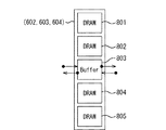
メモリ制御回路601から発行されるコマンドは最初のメモリモジュール602に伝達され、次に、メモリモジュール603、メモリモジュール604へと順次伝達される。この場合に、各メモリモジュール602、603、604の内部は、図8に示すような構造を有している。 A command issued from the memory control circuit 601 is transmitted to the first memory module 602, and then sequentially transmitted to the memory module 603 and the memory module 604. In this case, the inside of each of the memory modules 602, 603, and 604 has a structure as shown in FIG.
メモリモジュール602は、メモリモジュールのコアとなるメモリデバイス801、802、804及び805と、メモリ制御回路601から伝達されるコマンド、データをいったんバッファリングするためのバッファ803により構成される。メモリモジュール内のバッファ803では伝達されたコマンド、データが自身のメモリモジュールへのアクセスか、他のモジュールへのアクセスなのかの判定を行う。なお、メモリモジュール603及び604も上記と同様に構成される。
The memory module 602 includes
このときバッファ803が、自モジュール(即ち、バッファ803が属するメモリモジュール602)へのアクセスであると判定した場合にはコマンドをメモリモジュール602内のDRAM801、802、804、805へと分配する。また、他モジュール(即ち、メモリモジュール603等)へのアクセスであると判定した場合には、自モジュールへのアクセスを行わず、次段モジュール(メモリモジュール603)へと伝達する。このとき、書き込みデータに関してはコマンドと一緒に伝達し、読み込みデータに関しては、バッファ803を介してコマンドとは逆のメモリ制御回路601側へとデータを伝達する。
At this time, if the
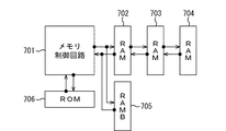
図6で示すような構成においては、同一のプロトコルに対応するメモリモジュール602、603及び604をカスケードに接続して回路を構成する。そのため、異なるプロトコルとして取り扱う他のROMモジュール606や、例えばSRAM等のメモリモジュール605を接続する場合には、メモリ制御回路601にカスケード接続したメモリモジュールとは別の接続口を設けてモジュールを接続する必要があった。そのため、メモリシステムを構成する際に、配線接続数が多くなり、接続に使用するピン数が増大してしまう問題がある。 In the configuration shown in FIG. 6, memory modules 602, 603 and 604 corresponding to the same protocol are connected in cascade to constitute a circuit. Therefore, when connecting another ROM module 606 treated as a different protocol, or a memory module 605 such as an SRAM, for example, a connection port different from that of the memory modules cascade-connected to the memory control circuit 601 is provided to connect the modules. There was a need. Therefore, when configuring the memory system, there is a problem that the number of wiring connections increases and the number of pins used for connection increases.
更に、配線接続に多くのピン数を必要とするため、メモリ制御回路601の構成に依存したシステム構成となり、ピン数が増大し、システム構成に制約がかかるといった問題がある。 Further, since a large number of pins are required for wiring connection, the system configuration depends on the configuration of the memory control circuit 601, and there is a problem that the number of pins increases and the system configuration is restricted.
また、図7に示すようにメモリ制御回路701からメモリモジュール702、703及び704への接続と、プロトコルの異なる別のメモリモジュール705をパラレルに接続した場合でも上記同様に問題がある。即ち、メモリ制御回路701からの配線性が悪くなり、同様に速度、プロトコルの異なるメモリモジュールを並列に接続する必要があるため、メモリのアクセス性能が低下するといった問題がある。
Further, as shown in FIG. 7, there is a problem similar to the above even when the connection from the
本発明は係る実情に鑑みてなされたものであり、異なるアクセスコマンドに対応するメモリモジュールを複数用いてカスケード接続させたメモリシステムを、その動作を保証しながら簡易な構成で提供することを目的とする。 The present invention has been made in view of the actual situation, and an object thereof is to provide a memory system in which a plurality of memory modules corresponding to different access commands are cascade-connected with a simple configuration while guaranteeing the operation thereof. To do.
本発明のメモリシステムは、アクセスコマンドを発行するメモリ制御手段と、前記メモリ制御手段からのアクセスコマンドを受け取ってバッファリングすると共に前記アクセスコマンドがメモリデバイスへのアクセスか否かを判断するバッファ部を備える複数のメモリモジュールがカスケード接続されているメモリ部と、を有し、前記メモリ部は、前記複数のメモリモジュールに含まれるROMを前記複数のメモリモジュールに含まれるRAMよりもレイテンシが大きくなるようにカスケード接続されていることを特徴とする。 The memory system of the present invention includes: a memory control means for issuing an access command, the buffer portion to which the access command with buffers receives an access command from said memory control means determines whether the access to memory device a plurality of memory modules comprising a has a memory unit are cascade-connected, and the memory unit, the latency is greater than the RAM contained a ROM included in the plurality of memory modules in said plurality of memory modules It is characterized by being cascade-connected .
本発明のメモリシステムは、複数のメモリモジュールをカスケード接続させる際に、その動作を保証しながら簡易に構成することができる。 The memory system of the present invention can be easily configured while guaranteeing the operation when a plurality of memory modules are cascade-connected .
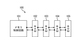
以下、図面を参照して本発明の実施の形態について説明する。本発明の実施の形態に係るメモリシステム100は、図1に示すようにメモリ制御回路101に、3組のメモリモジュール102〜104(以下、RAMと呼ぶ)及びROMモジュール105がカスケード接続されて構成される。
Embodiments of the present invention will be described below with reference to the drawings. As shown in FIG. 1, the
このときメモリ制御回路101から物理的距離が一番近いメモリモジュール102に対するレイテンシが一番小さく、物理的距離が一番遠いROMモジュール105に対するレイテンシが一番大きい構成となる。
At this time, the latency for the
図2に参照されるように、RAM102〜104はそれぞれ、メモリデバイス201、202、204及び205(以下、DRAMと呼ぶ)と、メモリ制御回路101から伝達されるアクセスコマンド及びデータを一旦バッファリングするためのバッファ203とを有して構成される。
As shown in FIG. 2, each of the
また、図3に参照されるように、ROMモジュール105は、メモリデバイス301及び302(以下、ROMと呼ぶ)と、メモリ制御回路101から伝達されるアクセスコマンド及びデータを一旦バッファリングするためのバッファ303とを有して構成される。
As shown in FIG. 3, the
本実施の形態のメモリシステム100において、アクセスコマンドやデータが伝達される場合、まず図1に示すメモリ制御回路101から共通のアクセスコマンド又はデータ(アクセスデータとデータとの双方の場合も含む)がRAM102に内蔵されるバッファ203に入力される。そして、バッファ203は、その入力された共通のアクセスコマンド又はデータを一時的にバッファリングすると共にその共通のアクセスコマンド又はデータが自身の属するRAM102が内蔵するDRAM201等へのアクセスか否かを判断する。
In the
そして、バッファ203が例えばアクセスコマンドが自身の属するRAM102が内蔵するDRAM201等へのアクセスであると判断した場合には、DRAM201、202、204及び205が認識可能なアクセスコマンドをそれぞれに分配する。
If the
一方、バッファ203がアクセスコマンドが他のRAM等(例えば、RAM103)へのアクセスであると判断した場合には、カスケード接続された次のRAM103へとアクセスコマンドを伝達する。なお、書き込みデータに関してはアクセスコマンドと一緒に伝達される。
On the other hand, when the
図4は、共通のアクセスコマンドから各メモリデバイスが認識可能なアクセスコマンドに変換するプロトコル変換回路401の構成例を示したものである。本実施の形態に係るメモリシステム100を構成するRAM102等のメモリモジュールは、このプロトコル変換回路401をそれぞれのバッファ203に有している。
FIG. 4 shows a configuration example of the
プロトコル変換回路401は、共通のコマンドをデコードするコマンドデコード回路402と、プロトコル変換回路401に接続されたDRAM等で構成されるメモリデバイス404を制御するメモリデバイス制御回路403とを有して構成される。ここで、メモリデバイス404は例えば図2におけるDRAM201等に相当する。また、コマンドデコード回路402及びメモリデバイス制御回路403を含んだ階層が、図2のバッファ203や図3のバッファ303等に内蔵される。
The
このプロトコル変換回路401を有する場合におけるメモリモジュール内の動作について以下説明する。まず、共通のアクセスコマンドがDRAMのプロトコルに準拠するものであった場合のプロトコル変換回路401における動作について説明する。
The operation in the memory module when the
コマンドデコード回路402では、共通のアクセスコマンドをデコードすることによってメモリデバイス制御回路403にプロトコルを把握させる。
The
メモリデバイス制御回路403では、メモリデバイス404が認識可能なアクセスコマンドを生成するため、メモリデバイス404が認識可能なアクセスコマンドを生成する。
The memory
ここで、共通のアクセスコマンドであるDRAMのプロトコルとアクセスコマンド変換後に必要となるプロトコルとが同一のDRAMのプロトコルであれば、プロトコル変換回路401ではプロトコル変換する必要が無い。その場合は、共通のアクセスコマンドをそのままメモリデバイス404へのアクセスコマンドとして使用することが可能となる。
Here, if the protocol of the DRAM, which is a common access command, and the protocol required after conversion of the access command are the same DRAM protocol, the
図1の場合には、RAM102、103及び104はDRAM201等で構成され、ROMモジュール105はROM301等で構成されているため、RAM102、103及び104の内部に搭載されるバッファ203では受け取った共通のアクセスコマンドをそのままDRAMに伝達することができる。
In the case of FIG. 1, the
一方、ROM105の内部に搭載されるバッファ303では、内蔵するプロトコル変換回路401によって、受け取った共通のアクセスコマンドをROM用アクセスコマンドに変換してROM301及び302に伝達する。
On the other hand, in the
ここで、共通のアクセスコマンド(DRAMのプロトコルに準拠するもの)からROM301及び302のアクセスコマンドに変換する場合について説明する。共通のアクセスコマンドでは、AddressはRowAddress、ColumnAddressが設定され、Commandには、Write/ReadCommnd のいずれかが使用されるとする。
Here, a case will be described in which a common access command (which conforms to the protocol of the DRAM) is converted into access commands for the
プロトコル変換回路401では、コマンドデコード回路402に入力されたRowAddressとColumnAddress からメモリデバイス404(即ち、ROM301等)が認識可能なアクセスコマンド、データとしてAddress を生成する。同様に、共通のアクセスコマンドのWrite/Readコマンドから、ROMデバイスのWrite/Read対応のコマンドに変換する。このとき、Pre−chargeや、refreshといったDRAM特有のプロトコルに依存したコマンドの場合には対応しない。
The
以上のようにメモリシステム100は、それを構成する各メモリモジュールのバッファに、共通のアクセスコマンド等を自モジュールが内蔵するメモリデバイスに対応するアクセスコマンド等に変換することのできるプロトコル変換回路401を設けた。これにより、異なるアクセスコマンドに対応するメモリモジュール(換言すれば、アクセスレイテンシの異なるメモリモジュール)を複数用いてカスケード接続させたメモリシステムをその動作が問題となることなく簡易に構成することができる。即ち、動作保証しながらカスケード接続が可能となるため、従来異なるアクセスコマンドに対応するメモリモジュールを複数用いて構成した際に問題となっていた接続口数、配線接続数、接続使用するピン数の増加を抑えることができ、簡易な構造でメモリシステムを実現できる。
As described above, the
なお、本実施形態においてメモリシステム100はRAM102〜104とROMモジュール105とで構成した例を挙げたが、そのモジュールの数は限定されるものではなく、またメモリモジュールが内蔵するメモリデバイスの数も限定されるものではない。また、図5に示すような異なるアクセスコマンドに対応するメモリモジュール502(RAM B)と、図1で示したRAM102〜104とをカスケード接続して構成したメモリシステムにおいても、それぞれのメモリモジュールにプロトコル変換回路401を設けることで、好適なメモリシステムを実現できる。
In this embodiment, the
また、本実施形態では、プロトコル変換回路401をそれぞれのメモリモジュールが有するバッファ部に内蔵する構成としたがこれに限定されるものではなく、バッファ部から独立した回路として構成してもよい。
In the present embodiment, the
また、本実施形態では、共通のコマンドをDRAMのプロトコルとしたが、共通のコマンドをDRAM以外のプロトコルにした場合であっても、各メモリモジュールのバッファ部にプロトコル変換回路401を組み込むことで、対応させることができる。
Further, in this embodiment, the common command is the DRAM protocol, but even if the common command is a protocol other than the DRAM, by incorporating the
また、種々のメモリモジュールを組み合わせた場合や、カスケード接続の接続順位に変更があった場合であっても、本実施形態にとらわれることなく好適に実施が可能である。 Further, even when various memory modules are combined or when the cascade connection order is changed, the embodiment can be suitably implemented without being restricted by the present embodiment.
100 メモリシステム
101 メモリ制御回路
102、103、104 メモリモジュール
105 ROMモジュール
201、202、204、205 メモリデバイス(DRAM)
203 バッファ
301、302 メモリデバイス(ROM)
303 バッファ
401 プロトコル変換回路
402 コマンドデコード回路
403 メモリデバイス制御回路
404 メモリデバイス
502 メモリモジュール
DESCRIPTION OF
203
Claims (6)
前記メモリ制御手段からのアクセスコマンドを受け取ってバッファリングすると共に前記アクセスコマンドがメモリデバイスへのアクセスか否かを判断するバッファ部を備える複数のメモリモジュールがカスケード接続されているメモリ部と、を有し、
前記メモリ部は、前記複数のメモリモジュールに含まれるROMを前記複数のメモリモジュールに含まれるRAMよりもレイテンシが大きくなるようにカスケード接続されていることを特徴とするメモリシステム。 Memory control means for issuing an access command;
Said memory unit access command is a plurality of memory modules comprising a buffer unit for determining whether access to the memory devices are cascaded together to buffer receives an access command from the memory control unit, the Have
The memory system is characterized in that the ROM included in the plurality of memory modules is cascade-connected so that the latency is larger than that of the RAM included in the plurality of memory modules .
Priority Applications (1)
| Application Number | Priority Date | Filing Date | Title |
|---|---|---|---|
| JP2006170404A JP5388406B2 (en) | 2006-06-20 | 2006-06-20 | Memory system |
Applications Claiming Priority (1)
| Application Number | Priority Date | Filing Date | Title |
|---|---|---|---|
| JP2006170404A JP5388406B2 (en) | 2006-06-20 | 2006-06-20 | Memory system |
Publications (3)
| Publication Number | Publication Date |
|---|---|
| JP2008003711A JP2008003711A (en) | 2008-01-10 |
| JP2008003711A5 JP2008003711A5 (en) | 2009-07-30 |
| JP5388406B2 true JP5388406B2 (en) | 2014-01-15 |
Family
ID=39008055
Family Applications (1)
| Application Number | Title | Priority Date | Filing Date |
|---|---|---|---|
| JP2006170404A Expired - Fee Related JP5388406B2 (en) | 2006-06-20 | 2006-06-20 | Memory system |
Country Status (1)
| Country | Link |
|---|---|
| JP (1) | JP5388406B2 (en) |
Families Citing this family (10)
| Publication number | Priority date | Publication date | Assignee | Title |
|---|---|---|---|---|
| US7539800B2 (en) * | 2004-07-30 | 2009-05-26 | International Business Machines Corporation | System, method and storage medium for providing segment level sparing |
| US7296129B2 (en) | 2004-07-30 | 2007-11-13 | International Business Machines Corporation | System, method and storage medium for providing a serialized memory interface with a bus repeater |
| US7331010B2 (en) | 2004-10-29 | 2008-02-12 | International Business Machines Corporation | System, method and storage medium for providing fault detection and correction in a memory subsystem |
| US7299313B2 (en) | 2004-10-29 | 2007-11-20 | International Business Machines Corporation | System, method and storage medium for a memory subsystem command interface |
| US7685392B2 (en) | 2005-11-28 | 2010-03-23 | International Business Machines Corporation | Providing indeterminate read data latency in a memory system |
| US7669086B2 (en) | 2006-08-02 | 2010-02-23 | International Business Machines Corporation | Systems and methods for providing collision detection in a memory system |
| US7870459B2 (en) | 2006-10-23 | 2011-01-11 | International Business Machines Corporation | High density high reliability memory module with power gating and a fault tolerant address and command bus |
| US7721140B2 (en) | 2007-01-02 | 2010-05-18 | International Business Machines Corporation | Systems and methods for improving serviceability of a memory system |
| WO2010029830A1 (en) * | 2008-09-12 | 2010-03-18 | 株式会社日立製作所 | Semiconductor device and information processing system |
| US7957173B2 (en) * | 2008-10-14 | 2011-06-07 | Mosaid Technologies Incorporated | Composite memory having a bridging device for connecting discrete memory devices to a system |
Family Cites Families (3)
| Publication number | Priority date | Publication date | Assignee | Title |
|---|---|---|---|---|
| JP4159415B2 (en) * | 2002-08-23 | 2008-10-01 | エルピーダメモリ株式会社 | Memory module and memory system |
| US7117316B2 (en) * | 2002-08-05 | 2006-10-03 | Micron Technology, Inc. | Memory hub and access method having internal row caching |
| JP2006146390A (en) * | 2004-11-17 | 2006-06-08 | Oki Data Corp | Memory bus conversion device and information processing system |
-
2006
- 2006-06-20 JP JP2006170404A patent/JP5388406B2/en not_active Expired - Fee Related
Also Published As
| Publication number | Publication date |
|---|---|
| JP2008003711A (en) | 2008-01-10 |
Similar Documents
| Publication | Publication Date | Title |
|---|---|---|
| JP5388406B2 (en) | Memory system | |
| KR100588599B1 (en) | Memory module and memory system | |
| KR101600447B1 (en) | Configurable bandwidth memory devices and methods | |
| US8806131B2 (en) | Multi-serial interface stacked-die memory architecture | |
| JP5052842B2 (en) | Memory system and method having point-to-point links | |
| US7965530B2 (en) | Memory modules and memory systems having the same | |
| US7463535B2 (en) | Memory modules and memory systems having the same | |
| US20090248969A1 (en) | Registered dimm memory system | |
| JP4527643B2 (en) | MEMORY DEVICE AND MEMORY DEVICE OPERATION METHOD | |
| JP2008140220A (en) | Semiconductor device | |
| JP2002133867A (en) | Semiconductor memory and system having memory module including this | |
| JP2009527829A (en) | Common analog interface for multiple processor cores | |
| JP2006228194A (en) | Composite memory chip capable of direct data transfer between internal memory devices and data transfer method | |
| JP4903481B2 (en) | Memory device structure | |
| JP2005353168A (en) | Memory interface circuit and memory interface method | |
| US10318464B1 (en) | Memory system and method for accessing memory system | |
| JP2005322371A (en) | Synchronous memory element | |
| JP2008041022A (en) | I/o device, communication device, servomotor control device, control system and robot system | |
| US6567321B2 (en) | Semiconductor memory device using dedicated command and address strobe signal and associated method | |
| US20030218918A1 (en) | Data writing method and memory system for using the method | |
| US7774535B2 (en) | Memory system and memory device | |
| KR20060116684A (en) | Memory systems, modules, controllers and methods using dedicated data and/or control busses | |
| JP2004127305A (en) | Memory controller | |
| US10545822B2 (en) | Semiconductor device | |
| JP2007164787A (en) | Memory system |
Legal Events
| Date | Code | Title | Description |
|---|---|---|---|
| A521 | Request for written amendment filed |
Free format text: JAPANESE INTERMEDIATE CODE: A523 Effective date: 20090612 |
|
| A621 | Written request for application examination |
Free format text: JAPANESE INTERMEDIATE CODE: A621 Effective date: 20090612 |
|
| A977 | Report on retrieval |
Free format text: JAPANESE INTERMEDIATE CODE: A971007 Effective date: 20120124 |
|
| A131 | Notification of reasons for refusal |
Free format text: JAPANESE INTERMEDIATE CODE: A131 Effective date: 20120131 |
|
| A521 | Request for written amendment filed |
Free format text: JAPANESE INTERMEDIATE CODE: A523 Effective date: 20120328 |
|
| A02 | Decision of refusal |
Free format text: JAPANESE INTERMEDIATE CODE: A02 Effective date: 20120515 |
|
| A61 | First payment of annual fees (during grant procedure) |
Free format text: JAPANESE INTERMEDIATE CODE: A61 Effective date: 20131008 |
|
| R151 | Written notification of patent or utility model registration |
Ref document number: 5388406 Country of ref document: JP Free format text: JAPANESE INTERMEDIATE CODE: R151 |
|
| LAPS | Cancellation because of no payment of annual fees |