KR20110028362A - 전기전자 부품용 복합재료 및 그것을 이용한 전기전자 부품 - Google Patents
전기전자 부품용 복합재료 및 그것을 이용한 전기전자 부품 Download PDFInfo
- Publication number
- KR20110028362A KR20110028362A KR1020117001422A KR20117001422A KR20110028362A KR 20110028362 A KR20110028362 A KR 20110028362A KR 1020117001422 A KR1020117001422 A KR 1020117001422A KR 20117001422 A KR20117001422 A KR 20117001422A KR 20110028362 A KR20110028362 A KR 20110028362A
- Authority
- KR
- South Korea
- Prior art keywords
- electrical
- insulating film
- metal
- plating
- composite material
- Prior art date
- Legal status (The legal status is an assumption and is not a legal conclusion. Google has not performed a legal analysis and makes no representation as to the accuracy of the status listed.)
- Granted
Links
Images

Classifications
-
- C—CHEMISTRY; METALLURGY
- C23—COATING METALLIC MATERIAL; COATING MATERIAL WITH METALLIC MATERIAL; CHEMICAL SURFACE TREATMENT; DIFFUSION TREATMENT OF METALLIC MATERIAL; COATING BY VACUUM EVAPORATION, BY SPUTTERING, BY ION IMPLANTATION OR BY CHEMICAL VAPOUR DEPOSITION, IN GENERAL; INHIBITING CORROSION OF METALLIC MATERIAL OR INCRUSTATION IN GENERAL
- C23C—COATING METALLIC MATERIAL; COATING MATERIAL WITH METALLIC MATERIAL; SURFACE TREATMENT OF METALLIC MATERIAL BY DIFFUSION INTO THE SURFACE, BY CHEMICAL CONVERSION OR SUBSTITUTION; COATING BY VACUUM EVAPORATION, BY SPUTTERING, BY ION IMPLANTATION OR BY CHEMICAL VAPOUR DEPOSITION, IN GENERAL
- C23C26/00—Coating not provided for in groups C23C2/00 - C23C24/00
-
- B—PERFORMING OPERATIONS; TRANSPORTING
- B05—SPRAYING OR ATOMISING IN GENERAL; APPLYING FLUENT MATERIALS TO SURFACES, IN GENERAL
- B05D—PROCESSES FOR APPLYING FLUENT MATERIALS TO SURFACES, IN GENERAL
- B05D7/00—Processes, other than flocking, specially adapted for applying liquids or other fluent materials to particular surfaces or for applying particular liquids or other fluent materials
- B05D7/14—Processes, other than flocking, specially adapted for applying liquids or other fluent materials to particular surfaces or for applying particular liquids or other fluent materials to metal, e.g. car bodies
- B05D7/16—Processes, other than flocking, specially adapted for applying liquids or other fluent materials to particular surfaces or for applying particular liquids or other fluent materials to metal, e.g. car bodies using synthetic lacquers or varnishes
-
- C—CHEMISTRY; METALLURGY
- C23—COATING METALLIC MATERIAL; COATING MATERIAL WITH METALLIC MATERIAL; CHEMICAL SURFACE TREATMENT; DIFFUSION TREATMENT OF METALLIC MATERIAL; COATING BY VACUUM EVAPORATION, BY SPUTTERING, BY ION IMPLANTATION OR BY CHEMICAL VAPOUR DEPOSITION, IN GENERAL; INHIBITING CORROSION OF METALLIC MATERIAL OR INCRUSTATION IN GENERAL
- C23C—COATING METALLIC MATERIAL; COATING MATERIAL WITH METALLIC MATERIAL; SURFACE TREATMENT OF METALLIC MATERIAL BY DIFFUSION INTO THE SURFACE, BY CHEMICAL CONVERSION OR SUBSTITUTION; COATING BY VACUUM EVAPORATION, BY SPUTTERING, BY ION IMPLANTATION OR BY CHEMICAL VAPOUR DEPOSITION, IN GENERAL
- C23C28/00—Coating for obtaining at least two superposed coatings either by methods not provided for in a single one of groups C23C2/00 - C23C26/00 or by combinations of methods provided for in subclasses C23C and C25C or C25D
- C23C28/02—Coating for obtaining at least two superposed coatings either by methods not provided for in a single one of groups C23C2/00 - C23C26/00 or by combinations of methods provided for in subclasses C23C and C25C or C25D only coatings only including layers of metallic material
- C23C28/021—Coating for obtaining at least two superposed coatings either by methods not provided for in a single one of groups C23C2/00 - C23C26/00 or by combinations of methods provided for in subclasses C23C and C25C or C25D only coatings only including layers of metallic material including at least one metal alloy layer
-
- C—CHEMISTRY; METALLURGY
- C23—COATING METALLIC MATERIAL; COATING MATERIAL WITH METALLIC MATERIAL; CHEMICAL SURFACE TREATMENT; DIFFUSION TREATMENT OF METALLIC MATERIAL; COATING BY VACUUM EVAPORATION, BY SPUTTERING, BY ION IMPLANTATION OR BY CHEMICAL VAPOUR DEPOSITION, IN GENERAL; INHIBITING CORROSION OF METALLIC MATERIAL OR INCRUSTATION IN GENERAL
- C23C—COATING METALLIC MATERIAL; COATING MATERIAL WITH METALLIC MATERIAL; SURFACE TREATMENT OF METALLIC MATERIAL BY DIFFUSION INTO THE SURFACE, BY CHEMICAL CONVERSION OR SUBSTITUTION; COATING BY VACUUM EVAPORATION, BY SPUTTERING, BY ION IMPLANTATION OR BY CHEMICAL VAPOUR DEPOSITION, IN GENERAL
- C23C28/00—Coating for obtaining at least two superposed coatings either by methods not provided for in a single one of groups C23C2/00 - C23C26/00 or by combinations of methods provided for in subclasses C23C and C25C or C25D
- C23C28/02—Coating for obtaining at least two superposed coatings either by methods not provided for in a single one of groups C23C2/00 - C23C26/00 or by combinations of methods provided for in subclasses C23C and C25C or C25D only coatings only including layers of metallic material
- C23C28/023—Coating for obtaining at least two superposed coatings either by methods not provided for in a single one of groups C23C2/00 - C23C26/00 or by combinations of methods provided for in subclasses C23C and C25C or C25D only coatings only including layers of metallic material only coatings of metal elements only
-
- C—CHEMISTRY; METALLURGY
- C25—ELECTROLYTIC OR ELECTROPHORETIC PROCESSES; APPARATUS THEREFOR
- C25D—PROCESSES FOR THE ELECTROLYTIC OR ELECTROPHORETIC PRODUCTION OF COATINGS; ELECTROFORMING; APPARATUS THEREFOR
- C25D3/00—Electroplating: Baths therefor
- C25D3/02—Electroplating: Baths therefor from solutions
- C25D3/12—Electroplating: Baths therefor from solutions of nickel or cobalt
-
- C—CHEMISTRY; METALLURGY
- C25—ELECTROLYTIC OR ELECTROPHORETIC PROCESSES; APPARATUS THEREFOR
- C25D—PROCESSES FOR THE ELECTROLYTIC OR ELECTROPHORETIC PRODUCTION OF COATINGS; ELECTROFORMING; APPARATUS THEREFOR
- C25D3/00—Electroplating: Baths therefor
- C25D3/02—Electroplating: Baths therefor from solutions
- C25D3/56—Electroplating: Baths therefor from solutions of alloys
- C25D3/562—Electroplating: Baths therefor from solutions of alloys containing more than 50% by weight of iron or nickel or cobalt
-
- C—CHEMISTRY; METALLURGY
- C25—ELECTROLYTIC OR ELECTROPHORETIC PROCESSES; APPARATUS THEREFOR
- C25D—PROCESSES FOR THE ELECTROLYTIC OR ELECTROPHORETIC PRODUCTION OF COATINGS; ELECTROFORMING; APPARATUS THEREFOR
- C25D5/00—Electroplating characterised by the process; Pretreatment or after-treatment of workpieces
- C25D5/10—Electroplating with more than one layer of the same or of different metals
- C25D5/12—Electroplating with more than one layer of the same or of different metals at least one layer being of nickel or chromium
-
- C—CHEMISTRY; METALLURGY
- C25—ELECTROLYTIC OR ELECTROPHORETIC PROCESSES; APPARATUS THEREFOR
- C25D—PROCESSES FOR THE ELECTROLYTIC OR ELECTROPHORETIC PRODUCTION OF COATINGS; ELECTROFORMING; APPARATUS THEREFOR
- C25D5/00—Electroplating characterised by the process; Pretreatment or after-treatment of workpieces
- C25D5/48—After-treatment of electroplated surfaces
-
- H—ELECTRICITY
- H05—ELECTRIC TECHNIQUES NOT OTHERWISE PROVIDED FOR
- H05K—PRINTED CIRCUITS; CASINGS OR CONSTRUCTIONAL DETAILS OF ELECTRIC APPARATUS; MANUFACTURE OF ASSEMBLAGES OF ELECTRICAL COMPONENTS
- H05K1/00—Printed circuits
- H05K1/02—Details
- H05K1/0213—Electrical arrangements not otherwise provided for
- H05K1/0237—High frequency adaptations
- H05K1/0243—Printed circuits associated with mounted high frequency components
-
- H—ELECTRICITY
- H05—ELECTRIC TECHNIQUES NOT OTHERWISE PROVIDED FOR
- H05K—PRINTED CIRCUITS; CASINGS OR CONSTRUCTIONAL DETAILS OF ELECTRIC APPARATUS; MANUFACTURE OF ASSEMBLAGES OF ELECTRICAL COMPONENTS
- H05K9/00—Screening of apparatus or components against electric or magnetic fields
- H05K9/0073—Shielding materials
- H05K9/0081—Electromagnetic shielding materials, e.g. EMI, RFI shielding
- H05K9/0084—Electromagnetic shielding materials, e.g. EMI, RFI shielding comprising a single continuous metallic layer on an electrically insulating supporting structure, e.g. metal foil, film, plating coating, electro-deposition, vapour-deposition
-
- H—ELECTRICITY
- H01—ELECTRIC ELEMENTS
- H01R—ELECTRICALLY-CONDUCTIVE CONNECTIONS; STRUCTURAL ASSOCIATIONS OF A PLURALITY OF MUTUALLY-INSULATED ELECTRICAL CONNECTING ELEMENTS; COUPLING DEVICES; CURRENT COLLECTORS
- H01R13/00—Details of coupling devices of the kinds covered by groups H01R12/70 or H01R24/00 - H01R33/00
- H01R13/02—Contact members
- H01R13/03—Contact members characterised by the material, e.g. plating, or coating materials
-
- H—ELECTRICITY
- H05—ELECTRIC TECHNIQUES NOT OTHERWISE PROVIDED FOR
- H05K—PRINTED CIRCUITS; CASINGS OR CONSTRUCTIONAL DETAILS OF ELECTRIC APPARATUS; MANUFACTURE OF ASSEMBLAGES OF ELECTRICAL COMPONENTS
- H05K2201/00—Indexing scheme relating to printed circuits covered by H05K1/00
- H05K2201/10—Details of components or other objects attached to or integrated in a printed circuit board
- H05K2201/10613—Details of electrical connections of non-printed components, e.g. special leads
- H05K2201/10954—Other details of electrical connections
- H05K2201/10969—Metallic case or integral heatsink of component electrically connected to a pad on PCB
-
- H—ELECTRICITY
- H05—ELECTRIC TECHNIQUES NOT OTHERWISE PROVIDED FOR
- H05K—PRINTED CIRCUITS; CASINGS OR CONSTRUCTIONAL DETAILS OF ELECTRIC APPARATUS; MANUFACTURE OF ASSEMBLAGES OF ELECTRICAL COMPONENTS
- H05K3/00—Apparatus or processes for manufacturing printed circuits
- H05K3/30—Assembling printed circuits with electric components, e.g. with resistors
- H05K3/32—Assembling printed circuits with electric components, e.g. with resistors electrically connecting electric components or wires to printed circuits
- H05K3/34—Assembling printed circuits with electric components, e.g. with resistors electrically connecting electric components or wires to printed circuits by soldering
- H05K3/341—Surface mounted components
-
- Y—GENERAL TAGGING OF NEW TECHNOLOGICAL DEVELOPMENTS; GENERAL TAGGING OF CROSS-SECTIONAL TECHNOLOGIES SPANNING OVER SEVERAL SECTIONS OF THE IPC; TECHNICAL SUBJECTS COVERED BY FORMER USPC CROSS-REFERENCE ART COLLECTIONS [XRACs] AND DIGESTS
- Y10—TECHNICAL SUBJECTS COVERED BY FORMER USPC
- Y10T—TECHNICAL SUBJECTS COVERED BY FORMER US CLASSIFICATION
- Y10T428/00—Stock material or miscellaneous articles
- Y10T428/12—All metal or with adjacent metals
- Y10T428/12493—Composite; i.e., plural, adjacent, spatially distinct metal components [e.g., layers, joint, etc.]
- Y10T428/12535—Composite; i.e., plural, adjacent, spatially distinct metal components [e.g., layers, joint, etc.] with additional, spatially distinct nonmetal component
- Y10T428/12556—Organic component
- Y10T428/12569—Synthetic resin
-
- Y—GENERAL TAGGING OF NEW TECHNOLOGICAL DEVELOPMENTS; GENERAL TAGGING OF CROSS-SECTIONAL TECHNOLOGIES SPANNING OVER SEVERAL SECTIONS OF THE IPC; TECHNICAL SUBJECTS COVERED BY FORMER USPC CROSS-REFERENCE ART COLLECTIONS [XRACs] AND DIGESTS
- Y10—TECHNICAL SUBJECTS COVERED BY FORMER USPC
- Y10T—TECHNICAL SUBJECTS COVERED BY FORMER US CLASSIFICATION
- Y10T428/00—Stock material or miscellaneous articles
- Y10T428/24—Structurally defined web or sheet [e.g., overall dimension, etc.]
- Y10T428/24802—Discontinuous or differential coating, impregnation or bond [e.g., artwork, printing, retouched photograph, etc.]
- Y10T428/24917—Discontinuous or differential coating, impregnation or bond [e.g., artwork, printing, retouched photograph, etc.] including metal layer
-
- Y—GENERAL TAGGING OF NEW TECHNOLOGICAL DEVELOPMENTS; GENERAL TAGGING OF CROSS-SECTIONAL TECHNOLOGIES SPANNING OVER SEVERAL SECTIONS OF THE IPC; TECHNICAL SUBJECTS COVERED BY FORMER USPC CROSS-REFERENCE ART COLLECTIONS [XRACs] AND DIGESTS
- Y10—TECHNICAL SUBJECTS COVERED BY FORMER USPC
- Y10T—TECHNICAL SUBJECTS COVERED BY FORMER US CLASSIFICATION
- Y10T428/00—Stock material or miscellaneous articles
- Y10T428/31504—Composite [nonstructural laminate]
- Y10T428/31678—Of metal
- Y10T428/31681—Next to polyester, polyamide or polyimide [e.g., alkyd, glue, or nylon, etc.]
Landscapes
- Chemical & Material Sciences (AREA)
- Engineering & Computer Science (AREA)
- Chemical Kinetics & Catalysis (AREA)
- Materials Engineering (AREA)
- Metallurgy (AREA)
- Organic Chemistry (AREA)
- Mechanical Engineering (AREA)
- Electrochemistry (AREA)
- Microelectronics & Electronic Packaging (AREA)
- Physics & Mathematics (AREA)
- Electromagnetism (AREA)
- Life Sciences & Earth Sciences (AREA)
- Wood Science & Technology (AREA)
- Electroplating Methods And Accessories (AREA)
- Laminated Bodies (AREA)
- Other Surface Treatments For Metallic Materials (AREA)
- Shielding Devices Or Components To Electric Or Magnetic Fields (AREA)
Abstract
Description
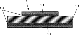
도 2는 금속기재와 절연피막과의 사이에 빈틈이 형성된 상태의 일례를 사시도에 의해 도시하는 개념도이다.
2 : 전기전자 부품
11, 21 : 금속기재
12, 22 : 절연피막
13 : 금속층
21a : 타발 가공면
23 : 빈틈
Claims (7)
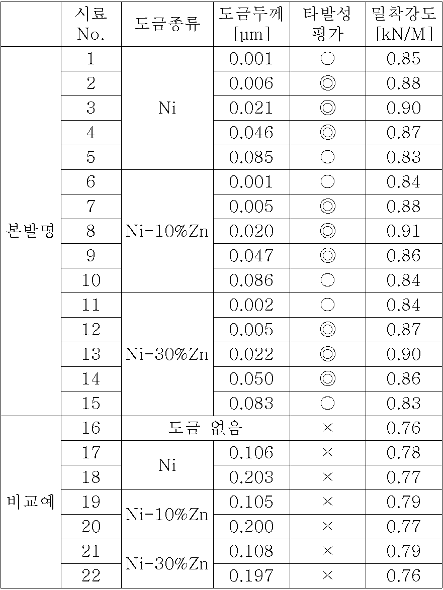
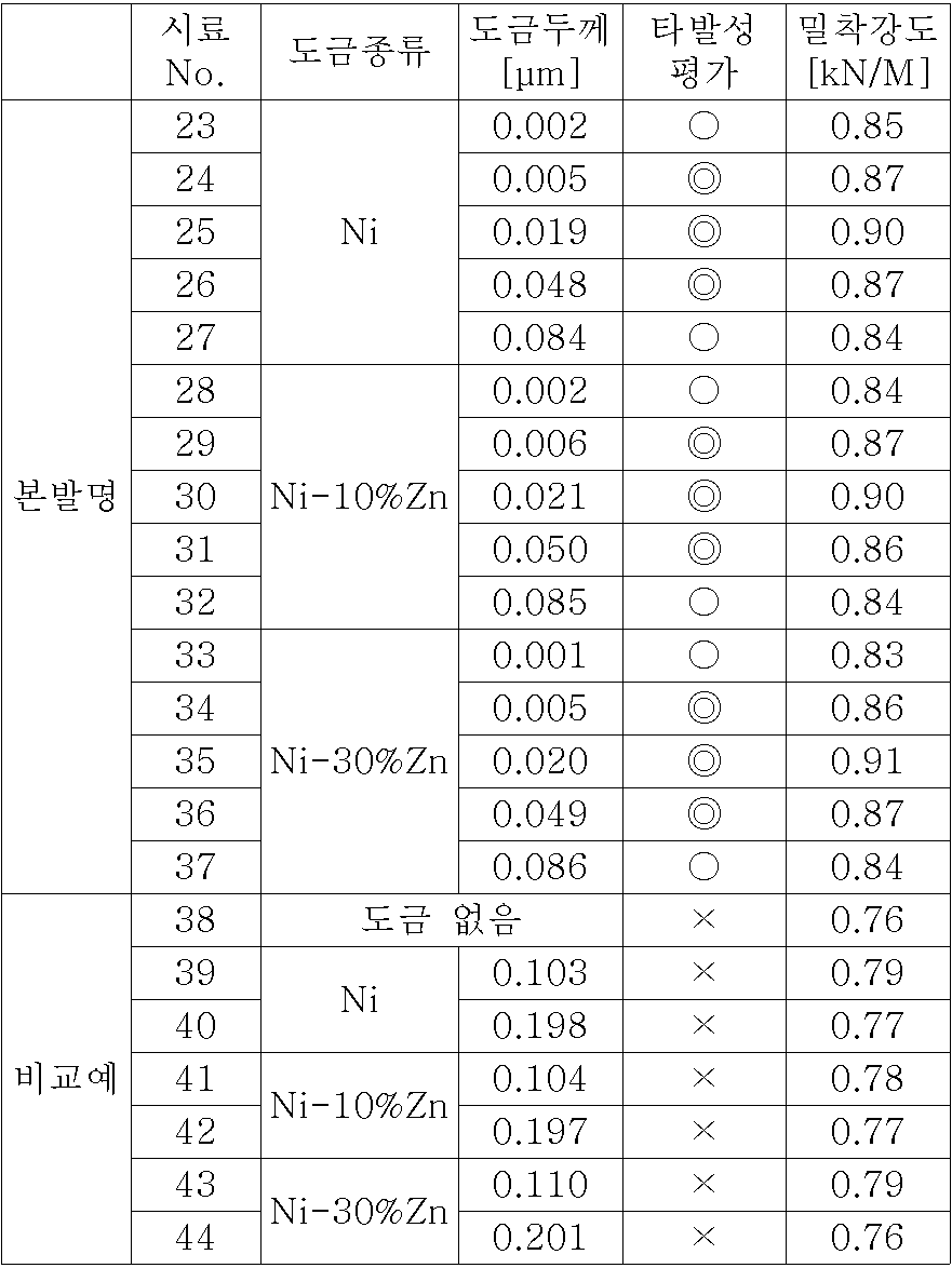
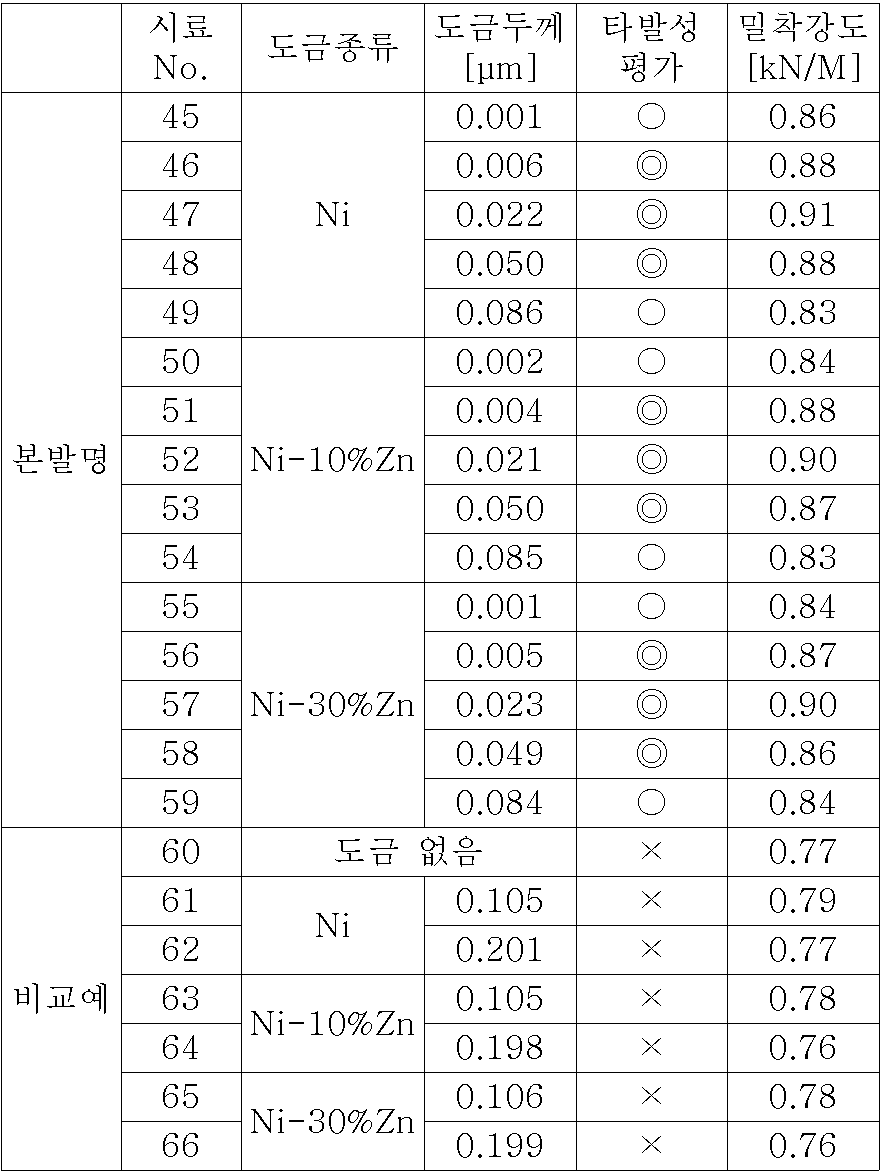
- 타발 가공되어 형성되는 전기전자 부품의 재료로서 이용되는, 금속기재상의 적어도 일부에 실질적으로 1층의 절연피막이 형성된 전기전자 부품용 복합재료로서, 상기 금속기재와 상기 절연피막과의 사이에, 상기 타발 가공 후의 재료 단부에서의 상기 절연피막의 박리 폭이 10㎛ 미만이 되도록 Ni 또는 Ni-Zn 합금으로 이루어지는 금속층이 개재되어 있는 것을 특징으로 하는 전기전자 부품용 복합재료.
- 제 1 항에 있어서, 상기 Ni 또는 Ni-Zn 합금으로 이루어지는 금속층의 두께가, 0.001㎛ 이상 0.1㎛ 미만인 것을 특징으로 하는 전기전자 부품용 복합재료.
- 제 1 항 또는 제 2 항에 있어서, 상기 절연피막이 폴리아미드이미드로 이루어지는 것을 특징으로 하는 전기전자 부품용 복합재료.
- 제 1 항 내지 제 3 항 중의 어느 한 항에 있어서, 상기 금속기재가, 구리계 금속재료에 의해 구성되어 있는 것을 특징으로 하는 전기전자 부품용 복합재료.
- 제 1 항 내지 제 4 항 중의 어느 한 항에 있어서, 상기 금속기재의 두께가, 0.06∼0.4mm인 것을 특징으로 하는 전기전자 부품용 복합재료.
- 제 1 항 내지 제 5 항 중의 어느 한 항에 기재된 전기전자 부품용 복합재료의 타발 가공 후에, 상기 금속기재상의 적어도 일부에 상기 절연피막이 잔존하도록 형성된 것을 특징으로 하는 전기전자 부품.
- 제 6 항에 있어서, 상기 전기전자 부품이, 타발 가공 후, 상기 절연피막이 형성되지 않은 개소(箇所)에 습식의 도금 처리가 행하여져서 형성된 것을 특징으로 하는 전기전자 부품.
Applications Claiming Priority (5)
| Application Number | Priority Date | Filing Date | Title |
|---|---|---|---|
| JPJP-P-2008-164851 | 2008-06-24 | ||
| JP2008164851 | 2008-06-24 | ||
| JPJP-P-2008-300181 | 2008-11-25 | ||
| JP2008300181 | 2008-11-25 | ||
| PCT/JP2009/061430 WO2009157457A1 (ja) | 2008-06-24 | 2009-06-23 | 電気電子部品用複合材料およびそれを用いた電気電子部品 |
Publications (2)
| Publication Number | Publication Date |
|---|---|
| KR20110028362A true KR20110028362A (ko) | 2011-03-17 |
| KR101336559B1 KR101336559B1 (ko) | 2013-12-03 |
Family
ID=41444523
Family Applications (1)
| Application Number | Title | Priority Date | Filing Date |
|---|---|---|---|
| KR1020117001422A Expired - Fee Related KR101336559B1 (ko) | 2008-06-24 | 2009-06-23 | 전기전자 부품용 복합재료 및 그것을 이용한 전기전자 부품 |
Country Status (7)
| Country | Link |
|---|---|
| US (1) | US8158269B2 (ko) |
| EP (1) | EP2302105A1 (ko) |
| JP (1) | JP4805409B2 (ko) |
| KR (1) | KR101336559B1 (ko) |
| CN (1) | CN102076889B (ko) |
| TW (1) | TWI449810B (ko) |
| WO (1) | WO2009157457A1 (ko) |
Families Citing this family (5)
| Publication number | Priority date | Publication date | Assignee | Title |
|---|---|---|---|---|
| JP5306641B2 (ja) * | 2006-12-27 | 2013-10-02 | 古河電気工業株式会社 | 電気電子部品用複合材料、電気電子部品および電気電子部品用複合材料の製造方法 |
| JP2011018873A (ja) * | 2009-05-22 | 2011-01-27 | Sony Ericsson Mobilecommunications Japan Inc | 電磁シールド方法および電磁シールド用フィルム |
| CN103921525B (zh) * | 2014-04-16 | 2016-01-13 | 曾芳勤 | 屏蔽罩内覆绝缘膜连续成型方法 |
| JP6627620B2 (ja) * | 2016-04-05 | 2020-01-08 | 株式会社オートネットワーク技術研究所 | コネクタ、接続状態検知システム、および、端子 |
| JP7524567B2 (ja) * | 2020-03-19 | 2024-07-30 | 三菱マテリアル株式会社 | 絶縁皮膜付き打ち抜き加工品及びその製造方法 |
Family Cites Families (9)
| Publication number | Priority date | Publication date | Assignee | Title |
|---|---|---|---|---|
| JP2802402B2 (ja) | 1990-02-20 | 1998-09-24 | 株式会社神戸製鋼所 | 打抜性及び密着性にすぐれた絶縁被膜を有する電磁鋼板の製造方法 |
| JP2991550B2 (ja) | 1991-10-31 | 1999-12-20 | 株式会社東芝 | 回転電機巻線の絶縁方法 |
| JPH05245432A (ja) | 1992-03-05 | 1993-09-24 | Yamaichi Electron Co Ltd | ポリイミド樹脂被覆板及びその製造方法 |
| JP2002237542A (ja) * | 2001-02-08 | 2002-08-23 | Sumitomo Electric Ind Ltd | 電子部品収納パッケージ用金属キャップ |
| CN1720351A (zh) * | 2002-12-03 | 2006-01-11 | 古河电气工业株式会社 | 用于电气或电子部件的金属材料 |
| JP2004197224A (ja) | 2002-12-03 | 2004-07-15 | Furukawa Electric Co Ltd:The | 電気電子部品用金属材料 |
| JP2006086513A (ja) * | 2004-08-16 | 2006-03-30 | Furukawa Electric Co Ltd:The | 電気電子部品ケースまたはシールドケースの材料及びその製造方法 |
| JP5215559B2 (ja) | 2006-12-27 | 2013-06-19 | エルジー ディスプレイ カンパニー リミテッド | 表示装置 |
| JP2008300181A (ja) | 2007-05-31 | 2008-12-11 | Panasonic Corp | プラズマ処理装置 |
-
2009
- 2009-06-23 WO PCT/JP2009/061430 patent/WO2009157457A1/ja not_active Ceased
- 2009-06-23 EP EP20090770167 patent/EP2302105A1/en not_active Withdrawn
- 2009-06-23 CN CN2009801244227A patent/CN102076889B/zh not_active Expired - Fee Related
- 2009-06-23 JP JP2010518029A patent/JP4805409B2/ja not_active Expired - Fee Related
- 2009-06-23 KR KR1020117001422A patent/KR101336559B1/ko not_active Expired - Fee Related
- 2009-06-24 TW TW98121119A patent/TWI449810B/zh not_active IP Right Cessation
-
2010
- 2010-12-23 US US12/977,147 patent/US8158269B2/en not_active Expired - Fee Related
Also Published As
| Publication number | Publication date |
|---|---|
| EP2302105A1 (en) | 2011-03-30 |
| TWI449810B (zh) | 2014-08-21 |
| JP4805409B2 (ja) | 2011-11-02 |
| CN102076889A (zh) | 2011-05-25 |
| WO2009157457A1 (ja) | 2009-12-30 |
| JPWO2009157457A1 (ja) | 2011-12-15 |
| US20110091739A1 (en) | 2011-04-21 |
| US8158269B2 (en) | 2012-04-17 |
| KR101336559B1 (ko) | 2013-12-03 |
| CN102076889B (zh) | 2013-05-08 |
| TW201005125A (en) | 2010-02-01 |
Similar Documents
| Publication | Publication Date | Title |
|---|---|---|
| KR101370137B1 (ko) | 전기전자 부품용 복합재료 및 그것을 이용한 전기전자 부품 | |
| US8110291B2 (en) | Composite material for electric/electronic part, production method thereof, and electric/electronic part | |
| CN101636514B (zh) | 印刷基板端子 | |
| JP4368931B2 (ja) | オス端子及びその製造方法 | |
| KR19990045402A (ko) | 금속 복합 밴드 제조 방법 | |
| KR101336559B1 (ko) | 전기전자 부품용 복합재료 및 그것을 이용한 전기전자 부품 | |
| CN111201842A (zh) | 印刷电路板和制造印刷电路板的方法 | |
| JP5185759B2 (ja) | 導電材及びその製造方法 | |
| KR20090102766A (ko) | 전기전자부품용 복합재료, 전기전자부품 및 전기전자부품용 복합재료의 제조방법 | |
| US20140308538A1 (en) | Surface treated aluminum foil for electronic circuits | |
| JP4316652B1 (ja) | 電気電子部品用複合材料、電気電子部品および電気電子部品用複合材料の製造方法 | |
| JP2006281453A (ja) | 電気電子部品用材料及びその製造方法 | |
| CN101617066A (zh) | 电气电子部件用复合材料、电气电子部件及电气电子部件用复合材料的制造方法 | |
| JP4776218B2 (ja) | 銅メタライズド樹脂及びその製造方法 | |
| JP2008179888A (ja) | 電気電子部品用複合材料、電気電子部品および電気電子部品用複合材料の製造方法 | |
| JP4856745B2 (ja) | フレキシブル基板用導体およびその製造方法並びにフレキシブル基板 | |
| JP5323418B2 (ja) | 電気電子部品用複合材料および電気電子部品 | |
| JP6446287B2 (ja) | Snめっき材およびその製造方法 | |
| CN120265834A (zh) | 复合材料、端子以及端子的制造方法 | |
| CN109910398A (zh) | 电气电子部件用复合材料以及使用其的电气电子部件 | |
| JP2008124048A (ja) | フレキシブル基板用導体およびその製造方法並びにフレキシブル基板 |
Legal Events
| Date | Code | Title | Description |
|---|---|---|---|
| PA0105 | International application |
St.27 status event code: A-0-1-A10-A15-nap-PA0105 |
|
| PG1501 | Laying open of application |
St.27 status event code: A-1-1-Q10-Q12-nap-PG1501 |
|
| A201 | Request for examination | ||
| P11-X000 | Amendment of application requested |
St.27 status event code: A-2-2-P10-P11-nap-X000 |
|
| P13-X000 | Application amended |
St.27 status event code: A-2-2-P10-P13-nap-X000 |
|
| PA0201 | Request for examination |
St.27 status event code: A-1-2-D10-D11-exm-PA0201 |
|
| E701 | Decision to grant or registration of patent right | ||
| PE0701 | Decision of registration |
St.27 status event code: A-1-2-D10-D22-exm-PE0701 |
|
| GRNT | Written decision to grant | ||
| PR0701 | Registration of establishment |
St.27 status event code: A-2-4-F10-F11-exm-PR0701 |
|
| PR1002 | Payment of registration fee |
St.27 status event code: A-2-2-U10-U12-oth-PR1002 Fee payment year number: 1 |
|
| PG1601 | Publication of registration |
St.27 status event code: A-4-4-Q10-Q13-nap-PG1601 |
|
| FPAY | Annual fee payment |
Payment date: 20161028 Year of fee payment: 4 |
|
| PR1001 | Payment of annual fee |
St.27 status event code: A-4-4-U10-U11-oth-PR1001 Fee payment year number: 4 |
|
| FPAY | Annual fee payment |
Payment date: 20171030 Year of fee payment: 5 |
|
| PR1001 | Payment of annual fee |
St.27 status event code: A-4-4-U10-U11-oth-PR1001 Fee payment year number: 5 |
|
| FPAY | Annual fee payment |
Payment date: 20181119 Year of fee payment: 6 |
|
| PR1001 | Payment of annual fee |
St.27 status event code: A-4-4-U10-U11-oth-PR1001 Fee payment year number: 6 |
|
| FPAY | Annual fee payment |
Payment date: 20191118 Year of fee payment: 7 |
|
| PR1001 | Payment of annual fee |
St.27 status event code: A-4-4-U10-U11-oth-PR1001 Fee payment year number: 7 |
|
| PC1903 | Unpaid annual fee |
St.27 status event code: A-4-4-U10-U13-oth-PC1903 Not in force date: 20201128 Payment event data comment text: Termination Category : DEFAULT_OF_REGISTRATION_FEE |
|
| R18-X000 | Changes to party contact information recorded |
St.27 status event code: A-5-5-R10-R18-oth-X000 |
|
| P22-X000 | Classification modified |
St.27 status event code: A-4-4-P10-P22-nap-X000 |
|
| P22-X000 | Classification modified |
St.27 status event code: A-4-4-P10-P22-nap-X000 |
|
| PC1903 | Unpaid annual fee |
St.27 status event code: N-4-6-H10-H13-oth-PC1903 Ip right cessation event data comment text: Termination Category : DEFAULT_OF_REGISTRATION_FEE Not in force date: 20201128 |