KR101422164B1 - Semiconductor device and display device - Google Patents
Semiconductor device and display device Download PDFInfo
- Publication number
- KR101422164B1 KR101422164B1 KR1020097014411A KR20097014411A KR101422164B1 KR 101422164 B1 KR101422164 B1 KR 101422164B1 KR 1020097014411 A KR1020097014411 A KR 1020097014411A KR 20097014411 A KR20097014411 A KR 20097014411A KR 101422164 B1 KR101422164 B1 KR 101422164B1
- Authority
- KR
- South Korea
- Prior art keywords
- thin film
- electrode
- film transistor
- shielding layer
- display device
- Prior art date
Links
Images


Classifications
-
- H—ELECTRICITY
- H10—SEMICONDUCTOR DEVICES; ELECTRIC SOLID-STATE DEVICES NOT OTHERWISE PROVIDED FOR
- H10K—ORGANIC ELECTRIC SOLID-STATE DEVICES
- H10K59/00—Integrated devices, or assemblies of multiple devices, comprising at least one organic light-emitting element covered by group H10K50/00
- H10K59/10—OLED displays
- H10K59/12—Active-matrix OLED [AMOLED] displays
- H10K59/126—Shielding, e.g. light-blocking means over the TFTs
-
- G—PHYSICS
- G02—OPTICS
- G02F—OPTICAL DEVICES OR ARRANGEMENTS FOR THE CONTROL OF LIGHT BY MODIFICATION OF THE OPTICAL PROPERTIES OF THE MEDIA OF THE ELEMENTS INVOLVED THEREIN; NON-LINEAR OPTICS; FREQUENCY-CHANGING OF LIGHT; OPTICAL LOGIC ELEMENTS; OPTICAL ANALOGUE/DIGITAL CONVERTERS
- G02F1/00—Devices or arrangements for the control of the intensity, colour, phase, polarisation or direction of light arriving from an independent light source, e.g. switching, gating or modulating; Non-linear optics
- G02F1/01—Devices or arrangements for the control of the intensity, colour, phase, polarisation or direction of light arriving from an independent light source, e.g. switching, gating or modulating; Non-linear optics for the control of the intensity, phase, polarisation or colour
- G02F1/13—Devices or arrangements for the control of the intensity, colour, phase, polarisation or direction of light arriving from an independent light source, e.g. switching, gating or modulating; Non-linear optics for the control of the intensity, phase, polarisation or colour based on liquid crystals, e.g. single liquid crystal display cells
- G02F1/133—Constructional arrangements; Operation of liquid crystal cells; Circuit arrangements
- G02F1/136—Liquid crystal cells structurally associated with a semi-conducting layer or substrate, e.g. cells forming part of an integrated circuit
- G02F1/1362—Active matrix addressed cells
- G02F1/136209—Light shielding layers, e.g. black matrix, incorporated in the active matrix substrate, e.g. structurally associated with the switching element
-
- G—PHYSICS
- G02—OPTICS
- G02F—OPTICAL DEVICES OR ARRANGEMENTS FOR THE CONTROL OF LIGHT BY MODIFICATION OF THE OPTICAL PROPERTIES OF THE MEDIA OF THE ELEMENTS INVOLVED THEREIN; NON-LINEAR OPTICS; FREQUENCY-CHANGING OF LIGHT; OPTICAL LOGIC ELEMENTS; OPTICAL ANALOGUE/DIGITAL CONVERTERS
- G02F1/00—Devices or arrangements for the control of the intensity, colour, phase, polarisation or direction of light arriving from an independent light source, e.g. switching, gating or modulating; Non-linear optics
- G02F1/01—Devices or arrangements for the control of the intensity, colour, phase, polarisation or direction of light arriving from an independent light source, e.g. switching, gating or modulating; Non-linear optics for the control of the intensity, phase, polarisation or colour
- G02F1/13—Devices or arrangements for the control of the intensity, colour, phase, polarisation or direction of light arriving from an independent light source, e.g. switching, gating or modulating; Non-linear optics for the control of the intensity, phase, polarisation or colour based on liquid crystals, e.g. single liquid crystal display cells
- G02F1/133—Constructional arrangements; Operation of liquid crystal cells; Circuit arrangements
- G02F1/136—Liquid crystal cells structurally associated with a semi-conducting layer or substrate, e.g. cells forming part of an integrated circuit
- G02F1/1362—Active matrix addressed cells
- G02F1/136218—Shield electrodes
-
- G—PHYSICS
- G02—OPTICS
- G02F—OPTICAL DEVICES OR ARRANGEMENTS FOR THE CONTROL OF LIGHT BY MODIFICATION OF THE OPTICAL PROPERTIES OF THE MEDIA OF THE ELEMENTS INVOLVED THEREIN; NON-LINEAR OPTICS; FREQUENCY-CHANGING OF LIGHT; OPTICAL LOGIC ELEMENTS; OPTICAL ANALOGUE/DIGITAL CONVERTERS
- G02F1/00—Devices or arrangements for the control of the intensity, colour, phase, polarisation or direction of light arriving from an independent light source, e.g. switching, gating or modulating; Non-linear optics
- G02F1/01—Devices or arrangements for the control of the intensity, colour, phase, polarisation or direction of light arriving from an independent light source, e.g. switching, gating or modulating; Non-linear optics for the control of the intensity, phase, polarisation or colour
- G02F1/13—Devices or arrangements for the control of the intensity, colour, phase, polarisation or direction of light arriving from an independent light source, e.g. switching, gating or modulating; Non-linear optics for the control of the intensity, phase, polarisation or colour based on liquid crystals, e.g. single liquid crystal display cells
- G02F1/133—Constructional arrangements; Operation of liquid crystal cells; Circuit arrangements
- G02F1/136—Liquid crystal cells structurally associated with a semi-conducting layer or substrate, e.g. cells forming part of an integrated circuit
- G02F1/1362—Active matrix addressed cells
- G02F1/1368—Active matrix addressed cells in which the switching element is a three-electrode device
-
- H—ELECTRICITY
- H10—SEMICONDUCTOR DEVICES; ELECTRIC SOLID-STATE DEVICES NOT OTHERWISE PROVIDED FOR
- H10K—ORGANIC ELECTRIC SOLID-STATE DEVICES
- H10K10/00—Organic devices specially adapted for rectifying, amplifying, oscillating or switching; Organic capacitors or resistors having a potential-jump barrier or a surface barrier
- H10K10/40—Organic transistors
- H10K10/46—Field-effect transistors, e.g. organic thin-film transistors [OTFT]
- H10K10/462—Insulated gate field-effect transistors [IGFETs]
- H10K10/466—Lateral bottom-gate IGFETs comprising only a single gate
-
- H—ELECTRICITY
- H10—SEMICONDUCTOR DEVICES; ELECTRIC SOLID-STATE DEVICES NOT OTHERWISE PROVIDED FOR
- H10K—ORGANIC ELECTRIC SOLID-STATE DEVICES
- H10K19/00—Integrated devices, or assemblies of multiple devices, comprising at least one organic element specially adapted for rectifying, amplifying, oscillating or switching, covered by group H10K10/00
- H10K19/10—Integrated devices, or assemblies of multiple devices, comprising at least one organic element specially adapted for rectifying, amplifying, oscillating or switching, covered by group H10K10/00 comprising field-effect transistors
-
- H—ELECTRICITY
- H10—SEMICONDUCTOR DEVICES; ELECTRIC SOLID-STATE DEVICES NOT OTHERWISE PROVIDED FOR
- H10K—ORGANIC ELECTRIC SOLID-STATE DEVICES
- H10K59/00—Integrated devices, or assemblies of multiple devices, comprising at least one organic light-emitting element covered by group H10K50/00
- H10K59/10—OLED displays
- H10K59/12—Active-matrix OLED [AMOLED] displays
- H10K59/125—Active-matrix OLED [AMOLED] displays including organic TFTs [OTFT]
-
- G—PHYSICS
- G02—OPTICS
- G02F—OPTICAL DEVICES OR ARRANGEMENTS FOR THE CONTROL OF LIGHT BY MODIFICATION OF THE OPTICAL PROPERTIES OF THE MEDIA OF THE ELEMENTS INVOLVED THEREIN; NON-LINEAR OPTICS; FREQUENCY-CHANGING OF LIGHT; OPTICAL LOGIC ELEMENTS; OPTICAL ANALOGUE/DIGITAL CONVERTERS
- G02F2202/00—Materials and properties
- G02F2202/02—Materials and properties organic material
Abstract
본 발명은, 바텀 게이트형 유기 박막 트랜지스터에서의 동작 특성을, 그 상층에 설치한 전극의 영향을 받지 않고 안정된 특성으로 유지할 수 있으며, 이를 구동 소자로 함으로써 신뢰성이 높은 표시가 가능한 표시 장치를 제공하는 것을 목적으로 한다. 기판(1) 상에 설치된 바텀 게이트형 박막 트랜지스터(Tr)와, 박막 트랜지스터(Tr)의 상부에 보호막(11) 및 층간 절연막(15)을 통하여 설치된 화소 전극(a)을 구비하고, 박막 트랜지스터(Tr)와 화소 전극(a) 사이에는, 이들 사이에 절연성을 유지하고, 도전성의 차폐층(13a)이 배치되어 있다.An object of the present invention is to provide a display device capable of maintaining highly stable operation characteristics in a bottom gate type organic thin film transistor with stable characteristics without being influenced by an electrode provided on the top of the bottom gate type organic thin film transistor, . A bottom gate type thin film transistor Tr provided on the substrate 1 and a pixel electrode a provided on the top of the thin film transistor Tr through a protective film 11 and an interlayer insulating film 15, Tr) and the pixel electrode (a), a conductive shielding layer 13a is disposed therebetween while maintaining the insulating property therebetween.
Description
본 발명은 반도체 장치 및 표시 장치에 관한 것이며, 특히 유기 반도체 박막을 사용한 반도체 장치, 및 이 반도체 장치를 사용한 표시 장치에 관한 것이다.The present invention relates to a semiconductor device and a display device, and more particularly to a semiconductor device using an organic semiconductor thin film and a display device using the semiconductor device.
박막 트랜지스터(thin film transistor: TFT)는, 액티브 매트릭스 구동형 평판 패널형 표시 장치에서의 화소 전극의 스위칭 소자로서 널리 사용되고 있다. 이와 같은 박막 트랜지스터에서, 채널층에 유기 반도체 박막을 사용한 유기 박막 트랜지스터는, 진공 처리 장치를 이용하지 않고 채널층(유기 반도체 박막)을 도포 성막할 수 있다. 그러므로, 채널층에 실리콘 박막을 사용한 무기 박막 트랜지스터에 비해, 저비용화에 유리하다.BACKGROUND ART Thin film transistors (TFT) are widely used as switching elements of pixel electrodes in an active matrix driven flat panel type display device. In such a thin film transistor, the organic thin film transistor using the organic semiconductor thin film in the channel layer can be formed by applying a channel layer (organic semiconductor thin film) without using a vacuum processing apparatus. Therefore, compared to an inorganic thin film transistor using a silicon thin film for a channel layer, it is advantageous in cost reduction.
상기 표시 장치에서, 유기 박막 트랜지스터가 설치된 구동 기판의 구성은 하기와 같다. 즉, 절연성 기판 상에서의 표시 영역에는, 주사선과 신호선이 절연성을 유지하며 교차 설치되어 있다. 그리고, 이들 배선의 교차 지점에, 예를 들면 바텀 게이트형의 유기 박막 트랜지스터가 설치되어 있다. 또한, 유기 박막 트랜지스터를 덮는 절연막에는 각 유기 박막 트랜지스터에 이르는 컨택트 홀이 형성되어 있고, 이 절연막 상에는 컨택트 홀을 통하여 각 유기 박막 트랜지스터에 접속된 화소 전극이 배열 형성되어 있다[이상, 예를 들면 일본 공개 특허 2006-86502호 공 보(특히 도 1∼ 3 및 관련 기재부) 참조].In the display device, the structure of the driving substrate provided with the organic thin film transistor is as follows. That is, in the display area on the insulating substrate, the scanning lines and the signal lines are provided so as to be insulated from each other and intersect with each other. At the intersection of these wirings, for example, a bottom gate type organic thin film transistor is provided. In the insulating film covering the organic thin film transistor, contact holes reaching the respective organic thin film transistors are formed. On the insulating film, pixel electrodes connected to the respective organic thin film transistors are arranged through contact holes (for example, Japan (See especially Figs. 1 to 3 and related description).
그런데, 유기 박막 트랜지스터의 구성은, 제조 단계의 용이성뿐만 아니라 캐리어의 이동 특성의 관점으로부터 바텀 게이트형이 유리하다고 여겨지고 있다. 즉, 기판 상에 성막된 유기 반도체 박막은, 상면 측과 비교하여 하면 측의 평탄성이 높고, 그러므로 하면 측에 채널부가 형성되는 바텀 게이트형에서 캐리어의 이동 특성이 양호하게 된다고 여겨지기 때문이다.However, the structure of the organic thin film transistor is considered to be advantageous from the viewpoint of not only the easiness of the manufacturing step but also the movement characteristics of the carrier, the bottom gate type being advantageous. That is, the organic semiconductor thin film formed on the substrate has higher flatness on the lower surface side as compared with the upper surface side, and therefore, it is considered that the carrier migration characteristics become better in the bottom gate type in which channel portions are formed on the lower surface side.
그러나, 바텀 게이트형의 유기 박막 트랜지스터를 사용한 반도체 장치 및 표시 장치에서는, 유기 박막 트랜지스터를 덮는 절연막 상의 전극이나 배선이, 채널부를 구성하는 유기 반도체 박막과 매우 근접한 거리에 배치되게 된다. 그러므로, 전극이나 배선 등에 인가되는 전위의 영향에 의해, 유기 박막 트랜지스터의 트랜지스터 특성이 쉽게 열화되는 문제가 발생한다.However, in the semiconductor device and the display device using the bottom gate type organic thin film transistor, the electrode or wiring on the insulating film covering the organic thin film transistor is disposed at a very close distance from the organic semiconductor thin film constituting the channel portion. Therefore, there arises a problem that the transistor characteristics of the organic thin film transistor easily deteriorate due to the influence of the potential applied to electrodes, wiring, and the like.
예를 들면, 표시 장치는, 유기 박막 트랜지스터의 상부에 화소 전극이 적층 배치됨으로써, 화소 전극에 인가되는 전위에 의해 유기 박막 트랜지스터가 전위 변조를 받는다. 이와 같은 전위 변조에 의해, 화소 전극의 구동이 불안정하게 되어 표시의 신뢰성이 열화된다. 또한, 유기 박막 트랜지스터를 스위칭시키기 위한 동작 전압의 진폭이 증대하여, 소비 전력의 상승이 일어난다.For example, in the display device, since the pixel electrodes are stacked on top of the organic thin film transistor, the organic thin film transistor undergoes electric potential modulation by the potential applied to the pixel electrode. By such electric potential modulation, the driving of the pixel electrode becomes unstable, and the reliability of display is deteriorated. Also, the amplitude of the operating voltage for switching the organic thin film transistor increases, and the power consumption increases.
또한, 특히 표시 장치가 유기 전계 발광 소자를 사용한 유기 EL(electroluminescence) 표시 장치이면, 유기 박막 트랜지스터 위쪽의 근접한 위치에, 화소 전극에 대향하는 공통 전극이 배치될 수도 있다. 이와 같은 경우라도, 공통 전극에 인가되는 전위에 의해 유기 박막 트랜지스터가 전위 변조를 받으므로, 전술한 바와 같은 문제가 발생한다.Furthermore, in particular, if the display device is an organic EL (electroluminescence) display device using an organic electroluminescent element, a common electrode facing the pixel electrode may be disposed at a position close to the upper side of the organic thin film transistor. Even in such a case, the organic thin film transistor undergoes electric potential modulation by the electric potential applied to the common electrode, so that the above-described problem arises.
따라서, 본 발명은, 바텀 게이트형의 유기 박막 트랜지스터에서의 동작 특성을, 그 상층에 설치된 전극의 영향을 받지 않고 안정된 특성을 유지할 수 있는 반도체 장치를 제공하는 것과, 반도체 장치를 구동 기판으로서 사용함으로써 신뢰성이 높은 표시가 가능한 표시 장치를 제공하는 것을 목적으로 한다.SUMMARY OF THE INVENTION It is therefore an object of the present invention to provide a semiconductor device capable of maintaining stable characteristics without being affected by electrodes provided on the upper layer of the organic thin film transistor of the bottom gate type by using the semiconductor device as a driving substrate And a display device capable of highly reliable display.
이와 같은 목적을 달성하기 위한 본 발명의 반도체 장치는, 기판 상에 설치된 바텀 게이트형의 박막 트랜지스터와, 상기 박막 트랜지스터의 상부에 절연막을 통하여 설치된 전극을 구비한 반도체 장치이며, 특히 박막 트랜지스터와 전극 사이에는, 이들 사이에 절연성을 유지하고, 도전성의 차폐층이 배치되어 있는 것을 특징으로 하고 있다.
또한, 본 발명의 반도체 장치는, 게이트 전극과, 상기 게이트 전극의 상층에 게이트 절연막을 통해 설치된 소스 전극 및 드레인 전극과, 유기 반도체 박막으로 구성되고, 상기 소스 전극과 드레인 전극 사이에 설치된 채널층을 기판 상에 가지는 바텀 게이트형(bottom gate type) 박막 트랜지스터; 및 상기 박막 트랜지스터의 상부에 절연막을 통하여 설치된 전극을 구비한 반도체 장치에 있어서, 상기 박막 트랜지스터와 상기 전극 사이에는, 도전성의 차폐층이 배치되고, 상기 차폐층은, 상기 박막 트랜지스터 및 상기 전극 각각의 사이에서 절연성을 유지하는 한편, 상기 채널층, 및 상기 소스 전극 및 드레인 전극의 전체 면을 덮는 상태로 형성되어 있는 것을 특징으로 하고 있다.A semiconductor device according to the present invention for achieving the above object is a semiconductor device having a bottom gate type thin film transistor mounted on a substrate and an electrode provided on the top of the thin film transistor through an insulating film. Is characterized in that a conductive shielding layer is disposed between them to maintain insulation.
A semiconductor device according to the present invention comprises a gate electrode, a source electrode and a drain electrode provided through a gate insulating film above the gate electrode, and a channel layer provided between the source electrode and the drain electrode, A bottom gate type thin film transistor on a substrate; And an electrode provided on the upper portion of the thin film transistor through an insulating film, wherein a conductive shielding layer is disposed between the thin film transistor and the electrode, and the shielding layer includes a thin film transistor And is formed so as to cover the entire surface of the channel layer and the source electrode and the drain electrode.
또한, 본 발명의 반도체 장치는, 전술한 반도체 장치를 구동 기판으로서 사용한 표시 장치이며, 박막 트랜지스터의 상부에 설치된 전극은, 상기 박막 트랜지스터에 접속된 화소 전극이거나, 또는 복수의 박막 트랜지스터에 대하여 공통으로 대향 배치된 공통 전극이다.
또한, 본 발명의 표시 장치는, 게이트 전극과, 상기 게이트 전극의 상층에 게이트 절연막을 통해 설치된 소스 전극 및 드레인 전극과, 유기 반도체 박막으로 구성되고, 상기 소스 전극과 드레인 전극 사이에 설치된 채널층을 기판 상에 가지는 바텀 게이트형 박막 트랜지스터; 및 상기 박막 트랜지스터의 상부에 절연막을 통하여 설치된 전극을 구비한 표시 장치에 있어서, 상기 박막 트랜지스터와 상기 전극 사이에는, 도전성의 차폐층이 배치되고, 상기 차폐층은, 상기 박막 트랜지스터 및 상기 전극 각각의 사이에서 절연성을 유지하는 한편, 상기 채널층의 전체 면 및 상기 소스 전극 및 드레인 전극의 일부를 덮는 상태로 형성되어 있는 것을 특징으로 하고 있다.Further, the semiconductor device of the present invention is a display device using the above-described semiconductor device as a driving substrate, and the electrode provided on the top of the thin film transistor is a pixel electrode connected to the thin film transistor or common to the plurality of thin film transistors And is a common electrode arranged to face each other.
A display device according to the present invention includes a gate electrode, a source electrode and a drain electrode provided through a gate insulating film over the gate electrode, and a channel layer provided between the source electrode and the drain electrode, A bottom gate type thin film transistor on a substrate; And an electrode provided on the upper portion of the thin film transistor through an insulating film, wherein a conductive shielding layer is disposed between the thin film transistor and the electrode, and the shielding layer includes a thin film transistor And is formed so as to cover the entire surface of the channel layer and a part of the source electrode and the drain electrode.
이와 같은 구성의 반도체 장치 및 표시 장치에서는, 바텀 게이트형의 박막 트랜지스터와 그 상부에 배치된 전극 사이에 도전성의 차폐층을 배치함으로써, 전극에 인가된 전위가 바텀 게이트형의 박막 트랜지스터의 채널층에 영향을 미치는 것이 방지된다.In the semiconductor device and the display device having such a structure, by disposing a conductive shielding layer between the bottom gate type thin film transistor and the electrode disposed on the bottom gate type thin film transistor, the electric potential applied to the electrode is applied to the channel layer of the bottom gate type thin film transistor Is prevented.
이상 설명한 바와 같이 본 발명에 의하면, 차폐층에 의해, 전극에 인가된 전위가, 바텀 게이트형의 박막 트랜지스터의 채널층에 영향을 미치는 것을 방지할 수 있으므로, 바텀 게이트형의 박막 트랜지스터에서의 동작 특성을, 그 상층에 설치한 전극의 영향을 받지 않고 안정되게 유지할 수 있다. 그리고, 화소 전극의 구동용으로서 바텀 게이트형의 박막 트랜지스터를 사용한 표시 장치에서, 신뢰성이 높은 표시를 행할 수 있게 된다.As described above, according to the present invention, since the shield layer can prevent the potential applied to the electrode from affecting the channel layer of the bottom gate type thin film transistor, Can be stably maintained without being influenced by the electrode provided on the upper layer. In the display device using the bottom gate type thin film transistor for driving the pixel electrode, highly reliable display can be performed.
도 1은, 본 발명이 적용되는 액정 표시 장치의 일구성예를 설명하기 위한 개략적인 회로 구성도이다.Fig. 1 is a schematic circuit configuration diagram for explaining a configuration example of a liquid crystal display device to which the present invention is applied.
도 2는, 제1 실시예의 액정 표시 장치의 특징부를 설명하기 위한 1 화소분의 단면도이다.2 is a cross-sectional view of one pixel for explaining a characteristic portion of the liquid crystal display device of the first embodiment.
도 3은, 제1 실시예의 액정 표시 장치의 특징부를 설명하기 위한 구동 기판 측의 4 화소분의 평면도이다.Fig. 3 is a plan view of four pixels on the driving substrate side for explaining the characteristic parts of the liquid crystal display device of the first embodiment.
도 4는, 제2 실시예의 액정 표시 장치의 특징부를 설명하기 위한 1 화소분의 단면도이다.4 is a cross-sectional view of one pixel for explaining a characteristic portion of the liquid crystal display device of the second embodiment.
도 5는, 제2 실시예의 액정 표시 장치의 특징부를 설명하기 위한 구동 기판 측의 4 화소분의 평면도이다.5 is a plan view of four pixels on the driving substrate side for explaining the characteristic parts of the liquid crystal display device of the second embodiment.
도 6은, 제3 실시예의 액정 표시 장치의 특징부를 설명하기 위한 1 화소분의 단면도이다.6 is a cross-sectional view of one pixel for explaining a characteristic portion of the liquid crystal display device of the third embodiment.
도 7은, 제3 실시예의 액정 표시 장치의 특징부를 설명하기 위한 구동 기판 측의 4 화소분의 평면도이다.7 is a plan view of four pixels on the drive substrate side for explaining the feature of the liquid crystal display device of the third embodiment.
도 8은, 본 발명이 적용되는 유기 EL 표시 장치의 일구성예를 설명하기 위하여 개략적으로 나타낸 회로 구성도이다.Fig. 8 is a circuit diagram schematically showing an exemplary configuration of an organic EL display device to which the present invention is applied.
도 9는, 제4 실시예의 유기 EL 표시 장치의 특징부를 설명하기 위한 1 화소분의 단면도이다.9 is a cross-sectional view of one pixel for explaining a characteristic portion of the organic EL display device of the fourth embodiment.
도 10은, 제4 실시예의 유기 EL 표시 장치의 특징부를 설명하기 위한 4 화소분의 주요부 평면도이다.10 is a plan view of a main portion for four pixels for explaining a characteristic portion of the organic EL display device of the fourth embodiment.
도 11은, 제5 실시예의 유기 EL 표시 장치의 특징부를 설명하기 위한 4 화소분의 주요부 평면도이다.11 is a plan view of a main portion for four pixels for explaining a characteristic portion of the organic EL display device of the fifth embodiment.
도 12는, 제6 실시예의 유기 EL 표시 장치의 특징부를 설명하기 위한 4 화소분의 주요부 평면도이다.12 is a plan view of a main portion for four pixels for explaining a characteristic portion of the organic EL display device of the sixth embodiment.
도 13은, 제7 실시예의 유기 EL 표시 장치의 특징부를 설명하기 위한 1 화소분의 단면도이다.13 is a cross-sectional view of one pixel for explaining a characteristic portion of the organic EL display device of the seventh embodiment.
도 14는, 제7 실시예의 유기 EL 표시 장치의 특징부를 설명하기 위한 4 화소분의 주요부 평면도를 나타낸다.14 is a plan view of a main part for four pixels for explaining a characteristic part of the organic EL display device of the seventh embodiment.
도 15는, 제8 실시예의 유기 EL 표시 장치의 특징부를 설명하기 위한 4 화소분의 주요부 평면도를 나타낸다.Fig. 15 is a plan view of a main portion for four pixels for explaining a characteristic portion of the organic EL display device of the eighth embodiment.
도 16은, 제9 실시예의 유기 EL 표시 장치의 특징부를 설명하기 위한 1 화소분의 단면도이다.16 is a cross-sectional view of one pixel for explaining a characteristic portion of the organic EL display device of the ninth embodiment.
도 17은, 제9 실시예의 유기 EL 표시 장치의 특징부를 설명하기 위한 4 화소분의 주요부 평면도를 나타낸다.17 is a plan view of a main part for four pixels for explaining a characteristic part of the organic EL display device of the ninth embodiment.
도 18은, 제10 실시예의 유기 EL 표시 장치의 특징부를 설명하기 위한 4 화소분의 주요부 평면도를 나타낸다.18 is a plan view of a main part for four pixels for explaining a characteristic part of the organic EL display device of the tenth embodiment.
도 19는, 제11 실시예의 유기 EL 표시 장치의 특징부를 설명하기 위한 1 화소분의 단면도이다.19 is a cross-sectional view of one pixel for explaining a characteristic portion of the organic EL display device of the eleventh embodiment.
도 20은, 제11 실시예의 유기 EL 표시 장치의 특징부를 설명하기 위한 4 화소분의 주요부 평면도를 나타낸다.20 is a plan view of a main part for four pixels for explaining a characteristic part of the organic EL display device of the eleventh embodiment.
도 21은, 제12 실시예의 유기 EL 표시 장치의 특징부를 설명하기 위한 4 화소분의 주요부 평면도이다.FIG. 21 is a plan view of a main portion for four pixels for explaining a characteristic portion of the organic EL display device of the twelfth embodiment. FIG.
도 22는, 제13 실시예의 유기 EL 표시 장치의 특징부를 설명하기 위한 4 화소분의 주요부 평면도이다.22 is a plan view of a main portion for four pixels for explaining a characteristic portion of the organic EL display device of the thirteenth embodiment.
도 23은, 제14 실시예의 유기 EL 표시 장치의 특징부를 설명하기 위한 1 화소분의 단면도이다.23 is a cross-sectional view of one pixel for explaining a characteristic portion of the organic EL display device of the fourteenth embodiment.
도 24는, 제14 실시예의 유기 EL 표시 장치의 특징부를 설명하기 위한 4 화소분의 주요부 평면도를 나타낸다.24 is a plan view of a main part for four pixels for explaining a characteristic portion of the organic EL display device of the fourteenth embodiment.
도 25는, 제15 실시예의 유기 EL 표시 장치의 특징부를 설명하기 위한 1 화소분의 단면도이다.25 is a cross-sectional view of one pixel for explaining a feature of the organic EL display device of the fifteenth embodiment.
도 26은, 제15 실시예의 유기 EL 표시 장치의 특징부를 설명하기 위한 4 화소분의 주요부 평면도를 나타낸다.26 is a plan view of a main part for four pixels for explaining a characteristic part of the organic EL display device of the fifteenth embodiment.
도 27은, 제16 실시예의 전기 영동 표시 장치의 특징부를 설명하기 위한 1 화소분의 단면도이다.27 is a cross-sectional view of one pixel for explaining a feature of the electrophoretic display device of the sixteenth embodiment.
도 28은, 제17 실시예를 설명하는 단면도이다.28 is a sectional view for explaining the seventeenth embodiment.
도 29는, 제18 실시예를 설명하는 흐름도이다.29 is a flowchart for explaining the eighteenth embodiment.
이하, 본 발명의 반도체 장치 및 표시 장치를 실시예를 도면을 참조하여 상세하게 설명한다. 그리고, 각 실시예에 있어서는, 본 발명의 반도체 장치를 구동 기판으로서 사용한 표시 장치의 구성을 설명한다.Hereinafter, embodiments of the semiconductor device and the display device of the present invention will be described in detail with reference to the drawings. In each of the embodiments, the structure of a display device using the semiconductor device of the present invention as a driving substrate will be described.
<제1 실시예>≪
제1 실시예에 있어서는, 액티브 매트릭스 방식의 액정 표시 장치에 본 발명을 적용한 실시예를 설명한다.In the first embodiment, an embodiment in which the present invention is applied to an active matrix type liquid crystal display device will be described.
도 1은 액정 표시 장치의 일구성예를 설명하기 위하여 개략적으로 나타낸 회로 구성도이다. 이 도면에 나타낸 바와 같이, 액정 표시 장치(40)의 기판(1) 상에는, 표시 영역(1a)과 그 주변 영역(1b)이 설정되어 있다. 표시 영역(1a)에는, 복수의 주사선(41)과 복수의 신호선(43)이 종횡으로 배선되어 있고, 각각의 교차부에 대응하여 1개의 화소가 설치된 화소 어레이부로서 구성되어 있다. 또한, 주변 영역(1b)에는, 주사선(41)을 주사 구동하는 주사선 구동 회로(45)와, 휘도 정보에 따른 영상 신호(즉 입력 신호)를 신호선(43)에 공급하는 신호선 구동 회로(47)가 배치되어 있다.1 is a circuit diagram schematically showing a configuration example of a liquid crystal display device. As shown in this drawing, on the
주사선(41)과 신호선(43)과의 각 교차부에 설치되는 화소 회로는, 예를 들면 박막 트랜지스터(Tr), 유지 용량(Cs) 및 화소 전극(a)으로 구성되어 있다. 그리고, 주사선 구동 회로(45)에 의한 구동에 의해, 박막 트랜지스터(Tr)를 통하여 신 호선(43)으로부터 기입된 영상 신호가 유지 용량(Cs)에 유지되고, 유지된 신호량에 따른 전압이 화소 전극(a)에 공급되고, 이 전압에 따라 액정층을 구성하는 액정 분자가 경사져서 표시광의 투과가 제어된다.The pixel circuit provided at each intersection of the
그리고, 이상과 같은 화소 회로의 구성은, 어디까지나 일례이며, 필요에 따라 화소 회로 내에 용량 소자를 설치하거나, 또한 복수의 트랜지스터를 설치하여 화소 회로를 구성해도 된다. 또한, 주변 영역(1b)에는, 화소 회로의 변경에 따라 필요한 구동 회로가 추가된다.The configuration of the pixel circuit as described above is merely an example. If necessary, a capacitor element may be provided in the pixel circuit, or a plurality of transistors may be provided to constitute the pixel circuit. Further, in the
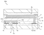
도 2에는, 본 제1 실시예의 액정 표시 장치(40a)의 특징부를 설명하기 위한 1 화소분의 단면도를 나타낸다. 또한, 도 3에는 본 제1 실시예의 액정 표시 장치(40a)의 특징부를 설명하기 위한 구동 기판 측의 4 화소분의 평면도를 나타낸다. 그리고, 평면도는, 설명을 위해 일부를 절단하며, 또한 전체를 덮는 절연성 재료로 이루어지는 막의 도시를 생략하고 있다. 그리고, 도 1과 동일한 구성 요소에는 동일한 부호를 부여하고 있다.Fig. 2 is a cross-sectional view of one pixel for explaining the characteristic portion of the liquid
이들 도면에 나타낸 바와 같이, 제1 실시예의 액정 표시 장치(40a)에서의 각 화소에는, 기판(1) 상에 게이트 전극(3), 게이트 절연막(5), 소스 전극(7s) 및 드레인 전극(7d), 및 유기 반도체 재료로 이루어지는 채널층(이하, 유기 채널층이라고 함)(9)을 전술한 순서로 적층한 바텀 게이트형의 박막 트랜지스터(Tr)가 설치되어 있다. 또한, 게이트 전극(3)과 같은 층에는 유지 용량(Cs)의 하부 전극(3c)이 형성되어 있고, 또한 소스 전극(7s) 및 드레인 전극(7d)과 같은 층에는, 드레인 전극(7d)으로부터 연장 형성된 유지 용량(Cs)의 상부 전극이 설치되어 있다. 또한, 평면도에 나타낸 바와 같이, 게이트 전극(3)은 같은 층에 의해 구성된 주사선(41)으로부터 연장되고, 소스 전극(7s)은 같은 층에 의해 구성된 신호선(43)으로부터 연장되고, 유지 용량(Cs)의 하부 전극(3c)은 복수 화소의 공통 전극으로서 배선되어 있다.As shown in these figures, in each pixel of the liquid
이상과 같은 박막 트랜지스터(Tr) 및 유지 용량(Cs)을 덮는 절연성 보호막(11) 상에, 본 제1 실시예의 특징인 도전성 차폐층(13a)이 설치되어 있다. 이 차폐층(13a)은, 적어도 유기 채널층(9) 상을 덮은 상태로 설치되어 있는 것으로 하고, 특히 본 제1 실시예에 있어서는 표시 영역의 전체면을 덮은 상태로 설치되어 있는 것으로 한다. 다만, 이 차폐층(13a)에는, 유지 용량(Cs)의 상부 전극에 노출되는 개구부(A)가 화소마다 설치되어 있는 것으로 한다.The
이와 같은 차폐층(13a)은, 표시 영역으로부터 주변 영역으로 인출되어 배선되고, 다른 전극 및 배선에 대하여 독립적으로 전위 제어할 수 있도록 구성되어 있다.Such a
이상과 같은 차폐층(13a)을 덮는 층간 절연막(15) 상에, 화소 전극(a)(평면도에서는 2점 쇄선으로 도시)이 설치되어 있다. 각 화소 전극(a)은, 개구부(A)의 내측에 설치한 컨택트부(17)를 통하여 유지 용량(Cs)의 상부 전극[드레인 전극(7d)]에 접속되어 있다.On the
그리고, 이들 화소 전극(a)을 덮은 상태에서, 예를 들면 표면 러빙(rubbing) 처리된 배향막(21)이 설치되고, 구동 기판(23)이 구성되어 있다.An
이상과 같이 구성된 구동 기판(23)을 구성하는 각 층은 일반적인 재료를 사 용하여 구성할 수 있고, 특히 이를 한정하지 않는다. 또한, 각 층은 기능을 해치지 않는 한, 복수의 재료로 이루어지는 다층 구조를 가지고 있어도 된다. 이러한 예로서는, 베이스부와의 밀착성 확보를 위해 전극 하부에 대한 밀착층의 도입이나, 전극 상에 대한 에지 스토퍼층의 도입, 가스 배리어성 확보나 연성(ductility) 확보를 위한 적층 메탈 구조 도입 등이 있다. 각 재료의 대표적인 예를 하기에 나타낸다.The layers constituting the
게이트 전극(3): 알미늄, 금, 금/크롬의 적층막, 은, 팔라듐, 나아가서는 이들의 적층막.Gate electrode (3): a laminated film of aluminum, gold, gold / chrome, silver, palladium, and further laminated films thereof.
게이트 절연막(5): 산화 실리콘, 질화 실리콘, 폴리비닐페놀, 폴리메틸메타크릴레이트(PMMA) 등.Gate insulating film 5: silicon oxide, silicon nitride, polyvinyl phenol, polymethyl methacrylate (PMMA), and the like.
소스·드레인 전극(7s, 7d): 금, 금/크롬의 적층막, 은, 백금, 팔라듐, 나아가서는 이들의 적층막.Source /
유기 채널층(9): 펜타센, 자이티오펜(xythiophene) 등의 티오펜 올리고머, 폴리티오펜 등.Organic channel layer (9): thiophene oligomers such as pentacene, xythiophene, polythiophene and the like.
보호막(11): 질화 실리콘, 산화 실리콘, 폴리파라자일렌, 폴리비닐알코올 등.Protective film (11): silicon nitride, silicon oxide, polyparaxylene, polyvinyl alcohol and the like.
차폐층(13a): 금, 금/크롬의 적층막, 은, 알루미늄, 나아가서는 이들의 적층막.
층간 절연막(15): 질화 실리콘, 폴리파라자일렌, PMMA 등의 아크릴계 수지, 폴리비닐알코올 등.Interlayer insulating film 15: acrylic resin such as silicon nitride, polyparaxylene, PMMA, polyvinyl alcohol, and the like.
화소 전극(a): 알미늄, 금, 금/크롬의 적층막, 은, 팔라듐, 이들의 적층막.The pixel electrode (a): a laminated film of aluminum, gold, gold / chromium, silver, palladium, or a laminated film thereof.
또한, 각 층의 형성 및 가공 방법에 대해서는, 공지의 기술을 널리 사용할 수 있다. 예를 들면, 진공 증착, 스퍼터링이나 CVD의 일반적인 성막 방법, 스핀 코트나 캡 코트, 스크린 인쇄, 잉크젯 인쇄 등의 용액을 사용한 성막 방법, 포토리소그래피법, 전자선 리소그래피법, 마이크로 프린팅법, 나노임프린트법 등의 패턴 전사 방법, 웨트 에칭법, 드라이 에칭법, 리프트 오프 등의 에칭 및 패턴 형성 기술을 조합시킬 수 있다. 이들을 조합시킬 경우, 필요한 가열이나 세정 등 일반적인 반도체 형성 기술도 당연히 사용할 수 있다.As to the formation and processing methods of the respective layers, well-known techniques can be widely used. For example, a general deposition method such as vacuum deposition, sputtering or CVD, a deposition method using a solution such as a spin coat, a cap coat, a screen printing, or an ink jet printing, a photolithography method, an electron beam lithography method, a micro printing method, A wet etching method, a dry etching method, a lift-off method, and the like. When these are combined, ordinary semiconductor forming techniques such as heating and cleaning as required can also be used.
그리고, 차폐층(13a)이 차광 기능을 갖추고 있는 경우, 차폐층(13a)의 형성 보다 나중의 단계에서 행해지는 리소그래피 등의 광을 사용한 프로세스에 대하여, 유기 채널층(9)의 내성이 향상된다.When the
또한, 각 층의 두께에 대해서도 기능을 해치지 않는 한 이를 한정하지 않는다. 예를 들면, 게이트 전극(3), 소스·드레인 전극(7s, 7d), 차폐층(13a), 화소 전극(a), 게이트 절연막(5), 및 유기 채널층(9)은, 1㎛ 이하, 보다 바람직하게는 500nm 이하이다. 또한, 보호막(11) 및 층간 절연막(15)은 5㎛ 이하, 보다 바람직하게는 3㎛ 이하이다.Further, the thickness of each layer is not limited as long as it does not impair the function. For example, the
또한, 화소 전극(a)과 유지 용량(Cs) 사이의 컨택트부(17)를 구성하는 접속 구멍의 형상 및 크기에 대해서도 한정하지 않는다. 이 경우, 층간 절연막(15)의 접속 구멍과 보호막(11)의 접속 구멍이, 형상 및 크기가 반드시 일치할 필요는 없고, 예를 들면 [층간 절연막(15)의 개구 형상 > 보호막(11)의 개구 형상]인 구성이 나, [층간 절연막의 개구 형상 < 보호막의 개구 형상]인 구성도 포함된다.The shape and size of the connection hole constituting the
또한, 기판(1)에 관해서도, 제조 프로세스에서의 열이력에 대하여 내열성을 가지는 범위에서, 특별히 재질이나 판 두께가 한정되지 않는다. 예를 들면, 유리 등의 경질 재료로부터, 폴리에테르술폰(PES)이나 폴리에틸렌나프탈레이트(PEN) 등의 연질 플라스틱 재료도 사용할 수 있다. 또한, 게이트 전극(3)보다 하층의 구조를 기판(1)으로 생각하면, 전술한 유리나 플라스틱 상에 보호막이나 버퍼층이 위치해도 된다. 예를 들면, 유리 기판 상에 질화 실리콘(SiNx) 박막이 가스 배리어의 목적으로 형성되어 있는 경우나, 플라스틱 필름 상에 SiNx나 표면 보호와 평탄화용의 아크릴계 박막 등이 설치되어 있는 구성이라도 된다.The material and thickness of the
또한, 구동 기판(23)의 제작 순서는 특별히 한정되지 않는다. 예를 들면, 화소 전극(a)과 유지 용량(Cs) 사이의 컨택트부(17)를 구성하는 접속 구멍을 보호막(11)에 형성하는 단계는, 차폐층(13a)을 형성하기 전, 차폐층(13a)을 형성한 후, 혹은 층간 절연막(15)에 형성하는 접속 구멍과 동시 중의 어느 때라도 행할 수 있다.The manufacturing procedure of the
이상과 같은 구동 기판(23)은, 화소 전극(a)을 반사 재료로 구성함으로써, 액정 표시 장치(40a)에서의 배면판으로서 사용되고 있다.The driving
이상과 같은 구동 기판(23)의 배향막(21) 측에는, 대향 기판(31)이 배치되어 있다. 이 대향 기판(31)은, 유리 기판과 같은 투명 기판으로 이루어지고, 구동 기판(23) 측을 향해 모든 화소에 공통인 대향 전극(33) 및 배향막(35)이 이 순서로 배치되어 있다. 그리고, 이와 같은 대향 기판(31) 측의 구성 재료에 대해서도, 일 반적인 액정 표시 장치의 구성 재료를 적용해도 된다.On the side of the
그리고, 이와 같은 구동 기판(23)과 대향 기판(31) 사이에, 여기서는 도시하지 않는 스페이서가 끼워지고, 또한 액정층(37)이 충전 밀봉되어 액정 표시 장치(40a)가 구성되어 있다. 그리고, 도면 중에는 명기하고 있지 않지만, 예를 들면, 대향 기판(31)의 외면 상에 반사 방지막 등의 외광의 반사를 억제하는 기능을 가지는 부위가 존재해도 되고, 이 경우는 상기 기능을 가지는 부위를 형성한 후, 구동 기판(23)과 대향 기판(31) 사이에 스페이서를 끼워서 액정층(37)을 충전 밀봉하는 조립 단계를 행하면 된다. 또한, 대향 기판(31) 측에는, 필요에 따라 컬러 필터 층을 설치해도 된다.A spacer (not shown) is sandwiched between the
이상과 같은 제1 실시예에 따른 구성의 액정 표시 장치(반도체 장치)(40a)에서는, 바텀 게이트형의 박막 트랜지스터(Tr)와 그 상부에 배치된 화소 전극(a) 사이에 도전성의 차폐층(13a)을 배치함으로써, 화소 전극(a)에 인가된 전위가 박막 트랜지스터(Tr)의 유기 채널층(9)에 영향을 미치는 것이 방지된다. 그러므로, 바텀 게이트형의 박막 트랜지스터(Tr)에서의 동작 특성을, 화소 전극(a)에 인가되는 전압에 영향을 받지 않고 안정되게 유지할 수 있게 된다. 이 결과, 화소 전극(a)에 인가되는 전압의 안정화가 도모되므로 신뢰성이 높은 표시를 행할 수 있다.In the liquid crystal display device (semiconductor device) 40a having the structure according to the first embodiment as described above, a conductive shielding layer (semiconductor device) 40a is formed between the bottom gate type thin film transistor Tr and the
또한, 표시 영역의 실질적으로 전체면이 차폐층(13a)으로 덮힌 구성이므로, 차폐층(13a)이, 유기 채널층(9)에 대하여 가장 높은 가스 배리어 성능을 나타낼 수 있다. 그러므로, 유기 채널층(9)의 열화가 방지되고, 박막 트랜지스터(Tr)의 신뢰성의 향상을 도모할 수 있다.Further, since the substantially entire surface of the display region is covered with the
또한, 유기 채널층(9)에 대향 배치된 차폐층(13a)의 전위를, 다른 전극에 대하여 독립적으로 제어할 수 있으므로, 이 차폐층(13a)에 인가되는 전위에 의해 박막 트랜지스터(Tr)의 동작 특성을 제어할 수도 있게 된다. 구체적인 일례로서는, 차폐층(13a)에 임의의 전위(예를 들면 0V)를 인가함으로써, 화소 전극(a)의 전위를 차폐하고, 박막 트랜지스터(Tr)의 안정 동작을 실현하며, 전력 절약화에 공헌한다. 또한, 동작 전압 내에서, 박막 트랜지스터(Tr)의 오프 전류와 온 전류의 조정이 가능해지므로, 이를 사용하여 표시 시의 콘트라스트의 제어를 행할 수 있게 된다.Since the potential of the
그리고, 제1 실시예에서는, 적어도 박막 트랜지스터(Tr)의 유기 채널층(9)을 덮은 상태로 설치된 차폐층(13a)이, 독립적으로 전위 제어할 수 있는 구성이면 되고, 차폐층(13a)은 패터닝되어 있어도 된다. 예를 들면, 동일한 색의 광을 추출하는 화소마다 차폐층(13a)을 패터닝해도 되고, 신호선(43)을 따라 적, 녹, 청색의 각 화소가 배열되어 있는 경우에는, 신호선(43)을 따라 차폐층(13a)을 패터닝하면 된다. 그리고, 각 색마다 차폐층(13a)에 인가하는 전위를 제어하는 구성으로 함으로써, 색조 보정을 행할 수 있게 된다.In the first embodiment, at least a
<제2 실시예>≪
도 4에는, 제2 실시예의 액정 표시 장치(40b)의 특징부를 설명하기 위한 1 화소분의 단면도를 나타낸다. 또한, 도 5에는 제2 실시예의 액정 표시 장치(40b)의 특징부를 설명하기 위한 구동 기판 측의 4 화소분의 평면도를 나타낸다. 그리고, 평면도는, 설명을 위해 일부를 잘라내고, 전체를 덮는 절연성 재료로 이루어지는 막의 도시는 생략하고 있다. 또한, 액정 표시 장치의 일구성예를 설명하기 위 한 개략적인 회로 구성은, 제1 실시예에서 도 1을 사용하여 설명한 구성과 동일해도 된다.Fig. 4 shows a cross-sectional view of one pixel for explaining the characteristic portion of the liquid
이들 도면에 나타낸 제2 실시예의 액정 표시 장치(40b)가, 도 2 및 도 3을 사용하여 설명한 제1 실시예의 액정 표시 장치와 다른 점은, 차폐층(13b)의 구성에 있으며, 그 외의 구성은 동일한 것으로 한다.The liquid
즉 제2 실시예의 액정 표시 장치(40b)에서의 차폐층(13b)은, 보호막(11)에 형성한 접속 구멍과 이 내부를 매립하는 도전성 재료로 이루어지는 컨택트부(11a)를 통하여 소스 전극(7s)에 접속되어 있는 점이 특징적이다. 다만, 이 차폐층(13b)은, 소스 전극(7s)에 접속되어 있으면 되므로, 컨택트부(11a)의 레이아웃을 고려하여 소스 전극(7s)으로부터 연장 설치된 신호선(43)의 부분에 접속되어 있어도 된다(평면도 참조). 또한, 1개의 신호선(43)을 공유하는 상태에서 복수의 박막 트랜지스터(Tr)를 덮는 각 차폐층(13b)은, 적어도 1개소에서 신호선(43)에 접속되어 있으면 되고, 그 접속 개소는 주변 영역이라도 된다.That is, the
각 차폐층(13b)은, 1개의 신호선(43)을 공유하는 박막 트랜지스터(Tr)를 덮는 부분마다 분할되어 있고, 적어도 박막 트랜지스터(Tr)의 유기 채널층(9)을 덮은 상태에서 신호선(43)을 따라 패터닝되어 있는 것으로 한다. 그리고, 각 차폐층(13b)은, 각 소스 전극(7s) 또는 그 연장 상의 신호선(43)에 접속되어 있으면 되므로, 화소마다 패터닝되어 있어도 된다.Each of the shielding
이상과 같은 제2 실시예에 따라 구성된 액정 표시 장치(반도체 장치)(40b)에도, 바텀 게이트형 박막 트랜지스터(Tr)와 그 상부에 배치된 화소 전극(a) 사이에 도전성 차폐층(13b)이 배치되어 있다. 그러므로, 제1 실시예와 마찬가지로, 바텀 게이트형 박막 트랜지스터(Tr)에서의 동작 특성이 안정되도록 유지할 수 있게 되고, 또한 화소 전극(a)에 인가되는 전압의 안정화가 도모되므로 신뢰성이 높은 표시를 행할 수 있게 된다.In the liquid crystal display (semiconductor device) 40b constructed in accordance with the second embodiment as described above, the
<제3 실시예>≪ Third Embodiment >
도 6에는, 본 제3 실시예의 액정 표시 장치(40c)의 특징부를 설명하기 위한 1 화소분의 단면도를 나타낸다. 또한, 도 7에는 본 제3 실시예의 액정 표시 장치(40c)의 특징부를 설명하기 위한 구동 기판 측의 4 화소분의 평면도를 나타낸다. 그리고, 평면도는, 설명을 위해 일부를 절단하고 있고, 전체를 덮는 절연성 재료로 이루어지는 막의 도시하지 생략하고 있다. 또한, 액정 표시 장치의 일구성예를 설명하기 위한 개략적인 회로 구성은, 제1 실시예에서 도 1을 사용하여 설명한 구성과 동일해도 된다.6 is a cross-sectional view of one pixel for explaining a characteristic portion of the liquid
이들 도면에 나타낸 제3 실시예의 액정 표시 장치(40c)가, 도 2∼도 5를 사용하여 설명한 제1 실시예 및 제2 실시예의 액정 표시 장치와 다른 점은, 차폐층(13c)의 구성에 있으며, 그 외의 구성은 동일한 것으로 한다.The liquid
즉, 제3 실시예의 액정 표시 장치(40c)에서의 차폐층(13c)은, 보호막(11) 및 게이트 절연막(5)에 형성된 접속 구멍과 이 내부를 매립하는 도전성 재료로 이루어지는 컨택트부(5a)를 통하여 게이트 전극(3)에 접속되어 있는 점이 특징적이다. 다만, 이 차폐층(13c)은, 게이트 전극(3)에 접속되어 있으면 되므로, 컨택트부(5a)의 레이아웃을 고려하여 게이트 전극(3)으로부터 연장 설치된 주사선(41)의 부분에 서 접속되어 있어도 된다(평면도 참조). 또한, 1개의 주사선(41)을 공유하는 상태에서 복수의 박막 트랜지스터(Tr)를 덮는 각 차폐층(13c)은, 적어도 1개소에서 주사선(41)에 접속되어 있으면 되고, 그 접속 개소는 주변 영역이라도 된다.That is, the
각 차폐층(13c)은, 1개의 주사선(41)을 공유하는 박막 트랜지스터(Tr)를 덮는 부분마다 분할되어 있고, 적어도 박막 트랜지스터(Tr)의 유기 채널층(9)을 덮은 상태에서 주사선(41)을 따라 패터닝되어 있는 것으로 한다. 그리고, 각 차폐층(13c)은, 각 게이트 전극(3) 또는 그 연장 상의 주사선(41)에 접속되어 있으면 되므로, 화소마다 패터닝되어 있어도 된다.Each of the shielding
이상과 같은 제3 실시예에 따라 구성된 액정 표시 장치(반도체 장치)(40c)에도, 바텀 게이트형 박막 트랜지스터(Tr)와 그 상부에 배치된 화소 전극(a) 사이에 도전성의 차폐층(13c)이 배치되어 있다. 그러므로, 제1 실시예와 마찬가지로, 바텀 게이트형 박막 트랜지스터(Tr)에서의 동작 특성을 안정되게 유지할 수 있게 되고, 또한 화소 전극(a)에 인가되는 전압의 안정화가 도모되므로 신뢰성이 높은 표시를 행할 수 있게 된다.The liquid crystal display device (semiconductor device) 40c constructed in accordance with the third embodiment described above also has the
또한, 유기 채널층(9)에 대향 배치된 차폐층(13c)을 게이트 전극(3)과 접속함으로써, Tr1에 대한 화소 전극(a)의 영향을 배제함과 동시에 트랜지스터의 구동 능력을 향상시킬 수 있다.By connecting the
<제4 실시예><Fourth Embodiment>
제4 실시예에서는, 발광 소자로서 유기 전계 발광 소자를 사용한 액티브 매트릭스 방식의 유기 EL 표시 장치에 본 발명을 적용한 실시예를 설명한다. 그리 고, 이하의 각 도면에서는, 전술한 제1 실시예 ∼ 제3 실시예와 동일한 구성 요소에는 동일한 부호를 부여하여 설명하기로 한다.In the fourth embodiment, an embodiment in which the present invention is applied to an active matrix type organic EL display device using an organic electroluminescent element as a light emitting element will be described. In each of the following drawings, the same constituent elements as those of the above-described first to third embodiments are denoted by the same reference numerals.
도 8은 유기 EL 표시 장치의 일구성예를 설명하기 위한 개략적인 회로 구성도이다. 이 도면에 나타낸 바와 같이, 유기 EL 표시 장치(50)의 기판(1) 상에는, 표시 영역(1a)과 그 주변 영역(1b)이 설정되어 있다. 표시 영역(1a)에는, 복수의 주사선(41)과 복수의 신호선(43)이 종횡으로 배선되어 있고, 각각의 교차부에 대응하여 1개의 화소가 설치된 화소 어레이부로서 구성되어 있다. 또한, 주변 영역(1b)에는, 주사선(41)을 주사 구동하는 주사선 구동 회로(45)와 휘도 정보에 따른 영상 신호(즉 입력 신호)를 신호선(43)에 공급하는 신호선 구동 회로(47)가 배치되어 있다.8 is a schematic circuit configuration diagram for explaining a configuration example of the organic EL display device. As shown in this drawing, on the
주사선(41)과 신호선(43)과의 각 교차부에 설치되는 화소 회로는, 예를 들면 스위칭용 박막 트랜지스터(Tr1), 구동용 박막 트랜지스터(Tr2), 유지 용량(Cs), 및 유기 전계 발광 소자(EL)로 구성되어 있다. 그리고, 주사선 구동 회로(45)에 의한 구동에 의해, 스위칭용 박막 트랜지스터(Tr1)를 통하여 신호선(43)으로부터 기입된 영상 신호가 유지 용량(Cs)에 유지되고, 유지된 신호량에 따른 전류가 구동용 박막 트랜지스터(Tr2)로부터 유기 전계 발광 소자(EL)에 공급되고, 이 전류값에 따른 휘도로 유기 전계 발광 소자(EL)가 발광한다. 그리고, 구동용 박막 트랜지스터(Tr2)와 유지 용량(Cs)은, 공통의 전원 공급선(Vcc)(49)에 접속되어 있다.The pixel circuit provided at each intersection of the
그리고, 이상과 같은 화소 회로의 구성은, 어디까지나 일례이며, 필요에 따라 화소 회로 내에 용량 소자를 설치하거나, 또한 복수의 트랜지스터를 설치하여 화소 회로를 구성해도 된다. 또한, 주변 영역(1b)에는, 화소 회로의 변경에 따라 필요한 구동 회로가 추가된다.The configuration of the pixel circuit as described above is merely an example. If necessary, a capacitor element may be provided in the pixel circuit, or a plurality of transistors may be provided to constitute the pixel circuit. Further, in the
도 9에는, 본 제4 실시예의 유기 EL 표시 장치(50a)의 특징부를 설명하기 위한 1 화소분의 단면도를 나타낸다. 또한, 도 10에는 본 제4 실시예의 유기 EL 표시 장치(50a)의 특징부를 설명하기 위한 주요부의 평면도를 나타낸다. 그리고, 평면도는, 설명을 위해 일부를 절단하고 있고, 또한 전체를 덮는 절연성 재료로 이루어지는 막의 도시는 생략하고 있다. 그리고, 도 8과 동일한 구성 요소에는 동일한 부호를 부여하고 있다.Fig. 9 shows a cross-sectional view of one pixel for explaining the characteristic parts of the organic
이들 도면에 나타낸 바와 같이, 제4 실시예의 유기 EL 표시 장치(50a)에서의 각 화소에는, 제1 실시예의 박막 트랜지스터와 동일한 적층 구성으로 이루어지는 바텀 게이트형 박막 트랜지스터(Tr1, Tr2), 및 유지 용량(Cs)이 설치되어 있다. 그리고, 단면도에서는 박막 트랜지스터(Tr1)만 도시하고 있다.As shown in these drawings, each pixel in the organic
그리고, 이상과 같은 박막 트랜지스터(Tr1, Tr2) 및 유지 용량(Cs)을 덮는 절연성의 보호막(11) 상에, 본 제4 실시예의 특징적인 도전성의 차폐층(13a)이 설치되어 있다. 이 차폐층(13a)은, 적어도 박막 트랜지스터(Tr1, Tr2)의 유기 채널층(9) 상을 덮은 상태에서 설치되어 있는 것으로 하고, 특히 본 제4 실시예에서는 표시 영역의 전체 면을 덮은 상태로 설치되어 있는 것으로 한다. 다만, 이 차폐층(13a)에는, 박막 트랜지스터(Tr2)의 소스(7s)[또는 드레인 전극(7d)]에 면하는 개구부(A)가 화소마다 설치되어 있는 것으로 한다.The characteristic
이와 같은 차폐층(13a)은, 표시 영역으로부터 주변 영역으로 인출되어 배선 되고, 다른 전극 및 배선에 대하여 독립적으로 전압 제어할 수 있는 구성으로 되어 있다.Such a
이상과 같은 차폐층(13a)을 덮는 층간 절연막(15) 상에는 화소 전극(a)(평면도에서는 2점 쇄선으로 도시)이 설치되어 있다. 각 화소 전극(a)은, 개구부(A)의 내측에 형성한 컨택트부(17)를 통하여 박막 트랜지스터(Tr2)의 소스(7s)[또는 드레인 전극(7d)]에 접속되어 있다. 이 화소 전극(a)은, 양극 또는 음극으로서 사용되며, 여기서는 또한 반사 전극으로서 형성되어 있는 것으로 한다.On the
이들 화소 전극(a)은, 중앙부를 넓게 노출시킨 상태에서 주위 에지부가 화소간 절연막(51)으로 덮혀져 있다. 이 화소간 절연막(51)은, 예를 들면 유기 절연 재료를 스핀 코트나 바 코터 등으로 도포하고, 포토리소그래피에 의해 가공함으로써 형성할 수 있다. 그리고, 화소간 절연막(51)으로부터 노출되어 있는 화소 전극(a) 상에는, 유기 EL 재료층(53)이 소정의 순서로 적층 성막되어 있다. 이 유기 EL 재료층(53)은, 진공 증착법이나 잉크젯법 등에 의해 형성된다. 이 때, 표시부에 다색 표시 기능을 부가하고자 하는 경우에는, 화소마다 표시 색을 색칠하여 분류하면 된다.In the pixel electrode (a), the peripheral edge portion is covered with the
또한, 화소간 절연막(51) 및 유기 EL 재료층(53) 상에는, 이들 층에 의해 화소 전극(a)에 대하여 절연성을 유지한 상태로 공통 전극(55)이 설치되어 있다. 이 공통 전극(55)은, 화소 전극(a)과는 정반대로 음극 또는 양극으로서 사용되며, 여기서는 또한 투명 전극으로서 구성되어 있는 것으로 한다. 이 공통 전극(55)은, 진공 증착법이나 스퍼터링법에 따라 형성된다. 그리고, 화소 전극(a)과 공통 전 극(55)에 의해 유기 EL 재료층(53)이 끼워진 각 부분이, 유기 전계 발광 소자(EL)로서 기능하는 부분이 된다.The
그리고, 이상과 같은 공통 전극(55) 상에, 광투과성을 가지는 접착제층(57)을 통하여 투명 기판(59)이 접합되어, 유기 EL 표시 장치(50a)가 구성되어 있다. 그리고, 여기서는 도시는 생략하였으나, 투명 기판(59) 측은, 예를 들면 컬러 필터나 반사 방지막 등의 화질 개량을 위한 층을 가지고 있어도 된다. 또한, 접착제층(57)은 반드시 모든 화소 상에 균일하게 존재할 필요는 없고, 예를 들면 주변 영역에만 존재하고 있어도 된다. 이 경우, 공통 전극(55)과 투명 기판(59) 사이에는 물리적 공간이 존재하지만, 동작에 지장이 없다면 그래도 상관없다.The
이와 같이 구성된 유기 EL 표시 장치(50a)는, 유기 전계 발광 소자(EL)에서의 발광광이 투명 기판(59) 측으로부터 추출되는 탑 이미션형이 된다.The organic
그리고, 이상과 같은 제4 실시예에 따라 구성된 유기 EL 표시 장치(50a)에도, 바텀 게이트형 박막 트랜지스터(Tr)와 그 상부에 배치된 화소 전극(a) 사이에 도전성의 차폐층(13a)이 배치되어 있다. 그러므로, 제1 실시예와 마찬가지로, 바텀 게이트형 박막 트랜지스터(Tr)에서의 동작 특성을 안정되게 유지할 수 있게 되고, 또한 화소 전극(a)에 인가되는 전압의 안정화가 도모되므로, 신뢰성이 높은 표시를 행할 수 있게 된다. 또한, 표시 영역의 실질적으로 전체 면이 차폐층(13a)으로 덮힌 구성이므로, 차폐층(13a)의 높은 가스 배리어성에 의해 유기 채널층(9)의 열화가 방지되어 신뢰성의 향상을 도모할 수 있다.The organic
또한, 박막 트랜지스터(Tr1, Tr2)에서의 유기 채널층(9)에 대향 배치된 차폐 층(13a)의 전위를, 다른 전극에 대하여 독립적으로 제어할 수 있으므로, 이 차폐층(13a)에 인가되는 전위에 의해 박막 트랜지스터(Tr1, Tr2)의 동작 특성을 제어할 수 있는 점도, 제1 실시예와 동일하다.The potential of the
<제5 실시예><Fifth Embodiment>
도 11에는, 본 제5 실시예의 유기 EL 표시 장치(50a)의 특징부를 설명하기 위한 구동 기판 측의 4 화소분의 평면도를 나타낸다. 이 도면에 나타낸 제5 실시예는, 제4 실시예의 변형예적인 실시예이다.11 is a plan view of four pixels on the driving substrate side for explaining the characteristic parts of the organic
도 11에 나타낸 바와 같이, 본 제5 실시예에서는, 차폐층(13a)이 박막 트랜지스터(Tr1)의 유기 채널층(9)을 덮는 부분과, 박막 트랜지스터(Tr2)의 채널층(9)을 덮는 부분으로 분할되어 패턴 형성되어 있다. 그리고, 박막 트랜지스터(Tr1)를 덮는 차폐층(13a)은, 서로 접속되고, 표시 영역으로부터 주변 영역으로 인출되어 배선되고, 다른 전극 및 배선에 대하여 독립적으로 전압 제어할 수 있는 구성으로 되어 있다. 마찬가지로, 박막 트랜지스터(Tr2)를 덮는 차폐층(13a)은, 서로 접속되고, 표시 영역으로부터 주변 영역으로 인출되어 배선되고, 다른 전극 및 배선에 대하여 독립적으로 전압 제어할 수 있는 구성으로 되어 있다. 그 외의 구성은, 제4 실시예와 동일한 것으로 한다.11, in the fifth embodiment, the
이와 같은 제5 실시예의 구성의 유기 EL 표시 장치(50a)에서는, 각 화소의 스위칭용 박막 트랜지스터(Tr1)와, 유기 전계 발광 소자(EL)에 흐르는 전류를 제어하는 구동용 박막 트랜지스터(Tr2)를 개별적으로 덮은 상태에서 패터닝된 각 차폐층(13a)에, 상이한 전위를 인가할 수 있다. 따라서, 각 박막 트랜지스터(Tr1, Tr2)의 동작 특성을 고려한 후, 각각의 동작에 적합한 제어를 행할 수 있게 된다.In the organic
<제6 실시예><Sixth Embodiment>
도 12에는, 제6 실시예에 따른 유기 EL 표시 장치(50a)의 특징부를 설명하기 위한 구동 기판 측의 4 화소분의 평면도를 나타낸다. 이 도면에 나타낸 제6 실시예는, 제4 실시예의 변형예적인 실시예의 또 다른 예이다.12 is a plan view of four pixels on the driving substrate side for explaining the characteristic parts of the organic
도 12에 나타낸 바와 같이, 본 제6 실시예에서는, 차폐층(13a)이 같은 색의 광을 추출하는 화소마다 분할되어 패턴 형성되어 있다. 도시한 예에서는, 신호선(43)을 따라 적, 녹, 청색의 각 화소가 배열되어 있는 예이며, 신호선(43)을 따라 차폐층(13a)이 패터닝되어 있는 경우를 예시하고 있다.As shown in Fig. 12, in the sixth embodiment, the
그리고, 패터닝된 차폐층(13a)은, 각 색마다 서로 접속되고, 표시 영역으로부터 주변 영역으로 인출되어 배선되고, 다른 전극 및 배선에 대하여 독립적으로 전압 제어할 수 있는 구성으로 되어 있다.The patterned
그리고, 이상과 같은 제6 실시예에 따라 구성된 유기 EL 표시 장치(50a)에서는, 적, 녹, 청색의 각 표시 색마다 패터닝된 각 차폐층(13a)에 상이한 전위를 인가할 수 있다. 즉, 적색용 차폐층, 녹색용 차폐층, 청색용 차폐층을 독립적으로 제어할 수 있으므로, 예를 들면 차폐층(13a)에 인가하는 전위를 제어함으로써 색조 보정을 행할 수 있게 된다.In the organic
<제7 실시예><Seventh Embodiment>
도 13에는, 제7 실시예의 유기 EL 표시 장치(50b)의 특징부를 설명하기 위한1 화소분의 단면도를 나타낸다. 또한, 도 14에는 제7 실시예의 유기 EL 표시 장 치(50b)의 특징부를 설명하기 위한 주요부 평면도를 나타낸다. 그리고, 평면도는, 설명을 위해 일부를 절단하고 있고, 또한 전체를 덮는 절연성 재료로 이루어지는 막의 도시는 생략하고 있다. 또한, 유기 EL 표시 장치의 일구성예를 설명하기 위한 개략적인 회로 구성은, 제4 실시예에서 도 8을 사용하여 설명한 구성과 동일하면 되고, 전술한 제4 실시예 ∼ 제6 실시예와 동일한 구성 요소에는 동일한 부호를 부여하여 설명을 행하기로 한다.Fig. 13 shows a cross-sectional view of one pixel for explaining a characteristic portion of the organic
이들 도면에 나타낸 제7 실시예의 유기 EL 표시 장치(50b)가, 도 9를 사용하여 설명한 제4 실시예 및 그 외의 실시예의 유기 EL 표시 장치와 다른 점은, 차폐층(13a, 13b)의 구성에 있으며, 그 외의 구성은 동일한 것으로 한다.The organic
즉, 제7 실시예의 유기 EL 표시 장치(50b)에는, 각 화소에 공통으로 설치된 차폐층(13a)에 의해 박막 트랜지스터(Tr2)가 덮혀져 있다. 이 차폐층(13a)은, 표시 영역으로부터 주변 영역으로 인출되어 배선되고, 다른 전극 및 배선에 대하여 독립적으로 전압 제어할 수 있는 구성으로 되어 있다.That is, in the organic
또한, 각 화소마다 패터닝된 차폐층(13b)에 의해 박막 트랜지스터(Tr1)가 덮혀져 있다. 이들 차폐층(13b)은, 보호막(11)에 형성된 접속 구멍과 이 내부를 매립하는 도전성 재료로 이루어지는 컨택트부(11a)를 통하여 박막 트랜지스터(Tr1)의 소스 전극(7s)에 접속되어 있다. 다만, 이 차폐층(13b)은, 박막 트랜지스터(Tr1)의 소스 전극(7s)에 접속되어 있으면 되므로, 컨택트부(11a)의 레이아웃을 고려하여 소스 전극(7s)으로부터 연장 형성된 신호선(43)의 부분에 접속되어 있어도 된다(평면도 참조).In addition, the thin film transistor Tr1 is covered by the
그리고, 각 차폐층(13b)은, 화소 레이아웃을 고려하여, 가능하면 1개의 신호선(43)을 공유하는 박막 트랜지스터(Tr1)를 덮는 부분마다 분할되어 있는 것이 바람직하고, 적어도 박막 트랜지스터(Tr1)의 유기 채널층(9)을 덮은 상태에서 신호선(43)을 따라 패터닝되어 있는 것도 바람직하다. 이 경우, 1개의 신호선(43)을 공유하는 상태에서 복수의 박막 트랜지스터(Tr)를 덮는 각 차폐층(13b)은, 적어도 1개소에서 신호선(43)에 접속되어 있으면 되고, 이 접속 개소가 주변 영역이라도 된다. 이 경우에도, 박막 트랜지스터(Tr2)를 덮는 차폐층(13a)은, 표시 영역의 주위둘레에서 서로 접속되어 공통으로 구동되는 구성이면 된다.It is preferable that each
이상과 같은 제7 실시예의 구성의 유기 EL 표시 장치(50b)에서는, 구동용 박막 트랜지스터(Tr2)의 차폐층(13a)이 모든 화소에서 공통으로 되어 있으므로, 한번에 모든 화소에서의 구동용 박막 트랜지스터(Tr2)를 제어하여 휘도를 조정할 수 있다. 또한, 스위칭용 박막 트랜지스터(Tr1)의 유기 채널층(9)에 대향 배치된 차폐층(13b)을 소스 전극(7s)과 접속시킴으로써, 화소 전극(a)의 전위의 Tr1에 대한 영향을 없애고, Tr1의 안정 동작과 동작 전압 저감이 가능하게 된다In the organic
<제8 실시예>≪ Eighth Embodiment >
도 15에는, 본 제8 실시예에 따른 유기 EL 표시 장치(50b)의 특징부를 설명하기 위한 구동 기판 측의 4 화소분의 평면도를 나타낸다. 이 도면에 나타낸 제8 실시예는, 제7 실시예의 변형예적인 실시예이다.Fig. 15 is a plan view of four pixels on the driving substrate side for explaining the characteristic parts of the organic
도 15에 나타낸 바와 같이, 본 제8 실시예에서는, 박막 트랜지스터(Tr2)를 덮는 차폐층(13a)이 동일한 색의 광을 추출하는 화소마다 분할되어 패턴 형성되어 있다. 도시한 예에서는, 신호선(43)을 따라 적, 녹, 청색의 각 화소가 배열되어 있는 예이며, 신호선(43)을 따라 차폐층(13a)이 패터닝되어 있는 경우를 예시하고 있다.As shown in Fig. 15, in the eighth embodiment, the
또한, 이와 같은 구성에 있어서도, 각 차폐층(13b)은, 1개의 신호선(43)을 공유하는 박막 트랜지스터(Tr1)를 덮는 부분마다 분할되어 있어도 되고, 적어도 박막 트랜지스터(Tr1)의 유기 채널층(9)을 덮은 상태에서 신호선(43)을 따라 패터닝되어 있어도 된다. 그리고, 1개의 신호선(43)을 공유하는 상태에서 복수의 박막 트랜지스터(Tr)를 덮는 각 차폐층(13b)은, 적어도 1개소에서 신호선(43)에 접속되어 있으면 되고, 그 접속 개소는 주변 영역이라도 된다.Also in this structure, each of the shielding layers 13b may be divided for each portion covering the thin film transistor Tr1 sharing one
그리고, 이상과 같은 제8 실시예에 따라 구성된 유기 EL 표시 장치(50b)에서는, 적, 녹, 청색의 각 표시 색마다 패터닝된 각 차폐층(13a)에 상이한 전위를 인가할 수 있다. 즉, 적색용 차폐층, 녹색용 차폐층, 청색용 차폐층을 독립적으로 제어할 수 있으므로, 예를 들면 차폐층(13a)에 인가하는 전위를 제어함으로써 색조 보정을 행할 수 있게 된다. 또한, 스위칭용 박막 트랜지스터(Tr1)의 유기 채널층(9)에 대향 배치된 차폐층(13b)을 소스 전극(7s)과 접속시킴으로써, 화소 전극(a)의 전위의 Tr1에 대한 영향을 없애고, Tr1의 안정 동작과 동작 전압 저감이 가능하게 된다.In the organic
<제9 실시예>≪ Example 9 &
도 16에는, 본 제9 실시예의 유기 EL 표시 장치(50c)의 특징부를 설명하기 위한 1 화소분의 단면도를 나타낸다. 또한, 도 17에는 본 제9 실시예의 유기 EL 표시 장치(50c)의 특징부를 설명하기 위한 주요부 평면도를 나타낸다. 그리고, 평면도는, 설명을 위해 일부를 절단하고 있고, 또한 전체를 덮는 절연성 재료로 이루어지는 막의 도시는 행하지 않고 있다. 또한, 유기 EL 표시 장치의 일구성예를 설명하기 위한 개략적인 회로 구성은, 제4 실시예에서 도 8을 사용하여 설명한 구성과 동일하면 되고, 전술한 제4 실시예 ∼ 제7 실시예와 동일한 구성 요소에는 동일한 부호를 부여하여 설명하기로 한다.16 is a cross-sectional view of one pixel for explaining a characteristic portion of the organic
이들 도면에 나타낸 제9 실시예의 유기 EL 표시 장치(50c)가, 도 9를 사용하여 설명한 제4 실시예 및 그 외의 실시예의 유기 EL 표시 장치와 다른 점은, 차폐층(13a, 13c)의 구성에 있으며, 그 외의 구성은 동일한 것으로 한다.The organic
즉, 제9 실시예의 유기 EL 표시 장치(50c)에는, 각 화소에 공통으로 설치된 차폐층(13a)에 의해 박막 트랜지스터(Tr2)가 덮혀져 있다. 이 차폐층(13a)은, 표시 영역으로부터 주변 영역에 인출되어 배선되어 다른 전극 및 배선에 대하여 독립적으로 전압 제어할 수 있는 구성으로 되어 있다.That is, in the organic
또한, 각 화소마다 패터닝된 차폐층(13c)에 의해 박막 트랜지스터(Tr1)가 덮혀져 있다. 이들 차폐층(13c)은, 보호막(11) 및 게이트 절연막(5)에 형성된 접속 구멍과 그 내부를 매립하는 도전성 재료로 이루어지는 컨택트부(5a)를 통하여 박막 트랜지스터(Tr1)의 게이트 전극(3)에 접속되어 있다. 다만, 이 차폐층(13c)은, 박막 트랜지스터(Tr1)의 게이트 전극(3)에 접속되어 있으면 되므로, 컨택트부(5a)의 레이아웃을 고려하여 주사선(41)의 부분에서 접속되어 있어도 된다(평면도 참조).In addition, the thin film transistor Tr1 is covered by the
그리고, 각 차폐층(13c)은, 화소 레이아웃을 고려하여, 가능하면 1개의 주사 선(41)을 공유하는 박막 트랜지스터(Tr)를 덮는 부분마다 분할되어 있는 것이 좋고, 적어도 박막 트랜지스터(Tr1)의 유기 채널층(9)을 덮은 상태에서 주사선(41)을 따라 패터닝되어 있는 것도 좋다. 이 경우, 1개의 주사선(41)을 공유하는 상태에서 복수의 박막 트랜지스터(Tr)를 덮는 각 차폐층(13c)은, 적어도 1개소에서 주사선(41)에 접속되어 있으면 되고, 그 접속 개소는 주변 영역이라도 된다. 이 경우에도, 박막 트랜지스터(Tr2)를 덮는 차폐층(13a)은, 표시 영역의 주위둘레에서 서로 접속되어 공통으로 구동되는 구성이면 된다.Each of the shielding layers 13c should preferably be divided for each portion covering the thin film transistor Tr that shares one
이상과 같이 구성된 제9 실시예에 따른 유기 EL 표시 장치(50c)에서는, 구동용 박막 트랜지스터(Tr2)의 차폐층(13a)이 모든 화소에서 공통으로 되어 있으므로, 한번에 모든 화소에서의 구동용 박막 트랜지스터(Tr2)를 제어하여 휘도를 조정할 수 있다. 또한, 유기 채널층(9)에 대향 배치된 차폐층(13c)을 게이트 전극(3)과 접속시킴으로써, Tr1에 대한 화소 전극(a)의 영향을 배제함과 동시에 트랜지스터의 구동 능력을 향상시킬 수 있다.In the organic
<제10 실시예><Tenth Embodiment>
도 18에는, 본 제10 실시예에 따른 유기 EL 표시 장치(50c)의 특징부를 설명하기 위한 구동 기판 측의 4 화소분의 평면도를 나타낸다. 이 도면에 나타낸 제10 실시예는, 제9 실시예의 변형예적인 실시예이다.Fig. 18 is a plan view of four pixels on the driving substrate side for explaining the characteristic parts of the organic
본 제10 실시예에서는, 도 18에 나타낸 바와 같이, 박막 트랜지스터(Tr2)를 덮는 차폐층(13a)이 동일한 색의 광을 추출하는 화소마다 분할되어 패턴 형성되어 있다. 도시한 예에서는, 신호선(43)을 따라 적, 녹, 청색의 각 화소가 배열되어 있는 예이며, 신호선(43)을 따라 차폐층(13a)이 패터닝되어 있는 경우를 예시하고 있다.In the tenth embodiment, as shown in Fig. 18, a
그리고, 이상과 같은 제10 실시예에 따라 구성된 유기 EL 표시 장치(50c)에서는, 적, 녹, 청색의 각 표시 색마다 패터닝된 각 차폐층(13a)에 상이한 전위를 인가할 수 있다. 즉, 적색용 차폐층, 녹색용 차폐층, 청색용 차폐층을 독립적으로 제어할 수 있으므로, 예를 들면, 차폐층(13a)에 인가하는 전위를 제어함으로써 색조 보정을 행할 수 있게 된다. 또한, 유기 채널층(9)에 대향 배치된 차폐층(13c)을 게이트 전극(3)과 접속시킴으로써, Tr1에 대한 화소 전극(a)의 영향을 배제함과 동시에 트랜지스터의 구동 능력을 향상시킬 수 있다.In the organic
<제11 실시예>≪ Eleventh Embodiment >
도 19에는, 본 제11 실시예의 유기 EL 표시 장치(60a)의 특징부를 설명하기 위한 1 화소분의 단면도를 나타낸다. 또한, 도 20에는 본 제11 실시예의 유기 EL 표시 장치(60a)의 특징부를 설명하기 위한 주요부 평면도를 나타낸다. 그리고, 평면도는, 설명을 위해 일부를 절단하고 있고, 또한 전체를 덮는 절연성 재료로 이루어지는 막의 도시는 생략하고 있다. 또한, 유기 EL 표시 장치의 일구성예를 설명하기 위한 개략적인 회로 구성은, 제4 실시예에서 도 8을 사용하여 설명한 구성과 동일해도 되고, 전술한 제4 실시예 ∼ 제10 실시예와 동일한 구성 요소에는 동일한 부호를 부여하여 설명하기로 한다.19 is a cross-sectional view of one pixel for explaining a characteristic portion of the organic
이들 도면에 나타낸 제11 실시예의 유기 EL 표시 장치(60a)가, 도 9 및 도 10을 사용하여 설명한 제4 실시예의 탑 이미션형 유기 EL 표시 장치와 다른 점은, 화소 전극(a)의 구성 및 차폐층(13a)의 구성에 있으며, 그 외의 구성은 동일한 것으로 한다.The organic
즉 제11 실시예의 유기 EL 표시 장치(60a)에서는, 박막 트랜지스터(Tr1, Tr2)의 소스 전극(7s) 및 드레인 전극(7d)과 동일 층에서 화소 전극(a)이 구성되어 있다. 각 화소 전극(a)은, 박막 트랜지스터(Tr2)의 소스 전극(7s)[또는 드레인 전극(7d)]으로부터 연장된 상태로 설치되어 있다. 또한, 이들 화소 전극(a)은, 양극 또는 음극으로서 사용되지만, 여기서는 가시광에 대한 광투과성을 가지거나 또는 반투과성을 가지는(가시광에 대하여 유한한 투과율을 가지는) 도전성 재료로 형성되어 있는 것으로 한다. 이 때, 화소 전극(a)은 가시광에 대하여 70% 정도의 투과율을 가지는 것이 바람직하다.That is, in the organic
또한, 박막 트랜지스터(Tr1, Tr2) 및 유지 용량(Cs)을 덮는 절연성 보호막(11)이, 화소 전극(a)의 중앙부를 넓게 노출시킨 상태에서 주위 에지부를 덮는 형상으로 패터닝된 화소간 절연막으로서 형성되어 있다.The insulating
그리고, 이 보호막(11) 상에 설치된 차폐층(13a)은, 적어도 박막 트랜지스터(Tr1, Tr2)의 유기 채널층(9) 상을 덮은 상태에서 설치되어 있는 것으로 하고, 특히 본 제11 실시예에서는 화소 전극(a)을 넓게 노출시키는 개구부(A)가 화소마다 설치되어 있는 것으로 한다. 이와 같은 차폐층(13a)은, 표시 영역으로부터 주변 영역으로 인출되어 배선되고, 다른 전극 및 배선에 대하여 독립적으로 전압 제어할 수 있는 구성으로 되어 있다.It is assumed that the
또한, 이 차폐층(13a)을 덮는 층간 절연막(15)도, 화소 전극(a)의 중앙부를 넓게 노출시킨 상태에서 화소 전극(a)의 주위 에지부를 덮는 형상으로 패터닝된 화소간 절연막으로서 형성되어 있다. 다만, 층간 절연막(15)에 의해 차폐층(13a)이 완전히 덮힌 상태로 되어 있는 것으로 한다.The
이와 같은 화소간 절연막을 구성하는 보호막(11)과 층간 절연막(15)에는, 연속된 패턴 에칭에 의해 화소 전극(a)을 노출시키는 개구 부분을 형성해도 된다.The opening portion for exposing the pixel electrode (a) by continuous pattern etching may be formed in the
그리고, 화소간 절연막으로부터 노출되어 있는 화소 전극(a) 상에 유기 EL 재료층(53)이 적층 성막되어 있는 점, 화소간 절연막과 유기 EL 재료층(53)에 의해 화소 전극(a)에 대하여 절연성을 유지한 상태로 공통 전극(55)가 설치되어 있는 점, 그리고, 화소 전극(a)과 공통 전극(55)으로 유기 EL 재료층(53)이 끼워진 각 부분이 유기 전계 발광 소자(EL)로서 기능하는 점은, 제4 실시예에서 설명한 바와 동일하다. 다만, 공통 전극(55)은, 여기서는 반사 전극으로서 구성되어 있는 것으로 한다.An organic
이와 같이 구성된 유기 EL 표시 장치(60a)는, 유기 전계 발광 소자(EL)에서의 발광광이 화소 전극(a)을 투과하여 기판(1) 측으로부터 추출되는 보텀 이미션형이 된다.The thus constituted organic
그리고, 이상과 같은 제11 실시예에 따라 구성된 유기 EL 표시 장치(60a)에서는, 바텀 게이트형 박막 트랜지스터(Tr1, Tr2)와 그 상부에 배치된 공통 전극(55) 사이에 도전성 차폐층(13a)이 배치되어 있다. 그러므로, 제1 실시예와 동일한 효과를 얻을 수 있다. 즉, 공통 전극(55)에 인가되는 전위에 영향을 받지 않고, 바텀 게이트형 박막 트랜지스터(Tr)에서의 동작 특성을 안정되게 유지할 수 있 게 되고, 또한 화소 전극(a)에 인가되는 전압의 안정화가 도모되므로, 신뢰성이 높은 표시를 행할 수 있게 된다. 또한, 표시 영역의 실질적으로 전체면이 차폐층(13a)으로 덮힌 구성이므로, 차폐층(13a)의 높은 가스 배리어성에 의해 유기 채널층(9)의 열화가 방지되어 신뢰성의 향상을 도모할 수 있다.In the organic
또한, 박막 트랜지스터(Tr1, Tr2)에서의 유기 채널층(9)에 대향 배치된 차폐층(13a)의 전위를, 다른 전극에 대하여 독립적으로 제어할 수 있으므로, 이 차폐층(13a)에 인가되는 전위에 의해 박막 트랜지스터(Tr1, Tr2)의 동작 특성을 제어할 수 있는 점도, 제1 실시예와 동일하다.The potential of the
<제12 실시예><Twelfth Embodiment>
도 21에는, 제12 실시예에 따른 유기 EL 표시 장치(60a)의 특징부를 설명하기 위한 구동 기판 측의 4 화소분의 평면도를 나타낸다. 이 도면에 나타낸 제12 실시예는, 제11 실시예의 변형예적인 실시예이다.Fig. 21 is a plan view of four pixels on the driving substrate side for explaining the characteristic parts of the organic
도 21에 나타낸 바와 같이, 본 제12 실시예에서는, 차폐층(13a)이 박막 트랜지스터(Tr1)의 유기 채널층(9)을 덮는 부분과, 박막 트랜지스터(Tr2)의 채널층(9)을 덮는 부분으로 분할되어 패턴 형성되어 있다. 그리고, 박막 트랜지스터(Tr1)를 덮는 차폐층(13a)은 서로 접속되고, 표시 영역으로부터 주변 영역으로 인출되어 배선되고, 다른 전극 및 배선에 대하여 독립적으로 전압 제어할 수 있는 구성으로 되어 있다. 마찬가지로, 박막 트랜지스터(Tr2)를 덮는 차폐층(13a)도 서로 접속되고, 표시 영역으로부터 주변 영역으로 인출되어 배선되고, 다른 전극 및 배선에 대하여 독립적으로 전압 제어할 수 있는 구성으로 되어 있다. 그 외의 구성은, 제11 실시예와 동일한 것으로 한다.As shown in Fig. 21, in the twelfth embodiment, the
이와 같은 제12 실시예에 따라 구성된 유기 EL 표시 장치(60a)에서는, 각 화소의 스위칭용 박막 트랜지스터(Tr1)와, 유기 전계 발광 소자(EL)에 흐르는 전류를 제어하는 구동용 박막 트랜지스터(Tr2)를 개별적으로 덮은 상태에서 패터닝된 각 차폐층(13a)에, 상이한 전위를 인가할 수 있다. 따라서, 각 박막 트랜지스터(Tr1, Tr2)의 동작 특성을 고려한 후에, 각각의 동작에 적합한 제어를 행할 수 있게 된다.The organic
<제13 실시예>≪ Thirteenth Embodiment &
도 22에는, 제13 실시예에 따른 유기 EL 표시 장치(60a)의 특징부를 설명하기 위한 구동 기판 측의 4 화소분의 평면도를 나타낸다. 이 도면에 나타낸 제13 실시예는, 제11 실시예의 변형예적인 실시예의 또 다른 예이다.22 is a plan view of four pixels on the driving substrate side for explaining the characteristic parts of the organic
도 22에 나타낸 바와 같이, 본 제13 실시예에서는, 차폐층(13a)이 동일한 색의 광을 추출하는 화소마다 분할되어 패턴 형성되어 있다. 도시한 예에서는, 신호선(43)을 따라 적, 녹, 청색의 각 화소가 배열되어 있는 예이며, 신호선(43)을 따라 차폐층(13a)이 패터닝되어 있는 경우를 예시하고 있다.As shown in Fig. 22, in the thirteenth embodiment, the
그리고, 패터닝된 차폐층(13a)은, 각 색마다 서로 접속되고, 표시 영역으로부터 주변 영역으로 인출되어 배선되고, 다른 전극 및 배선에 대하여 독립적으로 전압 제어할 수 있는 구성으로 되어 있다.The patterned
그리고, 이상과 같은 제22 실시예에 따라 구성된 유기 EL 표시 장치(60a)에서는, 적, 녹, 청색의 각 표시 색마다 패터닝된 각 차폐층(13a)에 상이한 전위를 인가할 수 있다. 즉, 적색용 차폐층, 녹색용 차폐층, 청색용 차폐층을 독립적으로 제어할 수 있으므로, 예를 들면 차폐층(13a)에 인가되는 전위를 제어함으로써 색조 보정을 행할 수 있게 된다.In the organic
<제14 실시예><Fourteenth Embodiment>
도 23에는, 제14 실시예에 따른 유기 EL 표시 장치(60b)의 특징부를 설명하기 위한 1 화소분의 단면도를 나타낸다. 또한, 도 24에는 본 제14 실시예의 유기 EL 표시 장치(60b)의 특징부를 설명하기 위한 주요부 평면도를 나타낸다. 그리고, 평면도는, 설명을 위해 일부를 절단하고 있고, 또한 전체를 덮는 절연성 재료로 이루어지는 막의 도시는 생략하고 있다. 또한, 유기 EL 표시 장치의 일구성예를 설명하기 위한 개략적인 회로 구성은, 제4 실시예에서 도 8을 사용하여 설명한 구성과 동일하면 되고, 전술한 실시예와 동일한 구성 요소에는 동일한 부호를 부여하여 설명하기로 한다.23 is a cross-sectional view of one pixel for explaining a characteristic portion of the organic
이들 도면에 나타낸 제14 실시예에 따른 유기 EL 표시 장치(60b)가, 도 19를 사용하여 설명한 제11 실시예 및 그 외의 실시예에 따른 보텀 이미션형 유기 EL 표시 장치와 다른 점은, 차폐층(13a, 13b)의 구성에 있으며, 그 외의 구성은 동일한 것으로 한다.The organic
즉, 제14 실시예에 따른 유기 EL 표시 장치(60b)에는, 각 화소에 공통으로 설치된 차폐층(13a)에 의해 박막 트랜지스터(Tr2)가 덮혀져 있다. 이 차폐층(13a)은 서로 접속되고, 표시 영역으로부터 주변 영역으로 인출되어 배선되고, 다른 전극 및 배선에 대하여 독립적으로 전압 제어할 수 있는 구성으로 되어 있다.That is, in the organic
또한, 각 화소마다 패터닝된 차폐층(13b)에 의해 박막 트랜지스터(Tr1)가 덮혀져 있다. 이들 차폐층(13b)은, 보호막(11)에 형성된 접속 구멍과 그 내부를 매립하는 도전성 재료로 이루어지는 컨택트부(11a)를 통하여 박막 트랜지스터(Tr1)의 소스 전극(7s)에 접속되어 있다. 다만, 이 차폐층(13b)은, 박막 트랜지스터(Tr1)의 소스 전극(7s)에 접속되어 있으면 되므로, 컨택트부(11a)의 레이아웃을 고려하여 소스 전극(7s)으로부터 연장 설치된 신호선(43)의 부분에 접속되어 있어도 된다(평면도 참조).In addition, the thin film transistor Tr1 is covered by the
그리고, 각 차폐층(13b)은, 화소 레이아웃을 고려하여, 가능하면 1개의 신호선(43)을 공유하는 박막 트랜지스터(Tr1)를 덮는 부분마다 분할되어 있는 것이 바람직하고, 적어도 박막 트랜지스터(Tr1)의 유기 채널층(9)을 덮은 상태에서 신호선(43)을 따라 패터닝되어 있는 것도 바람직하다. 이 경우, 1개의 신호선(43)을 공유하는 상태에서 복수의 박막 트랜지스터(Tr)를 덮는 각 차폐층(13b)은, 적어도 1개소에서 신호선(43)에 접속되어 있으면 되고, 그 접속 개소는 주변 영역이라도 된다. 이 경우에도, 박막 트랜지스터(Tr2)를 덮는 차폐층(13a)은, 표시 영역의 주위둘레에서 서로 접속되어 공통으로 구동되는 구성이면 된다.It is preferable that each
이상과 같은 제14 실시예의 구성의 유기 EL 표시 장치(60b)에서는, 구동용 박막 트랜지스터(Tr2)의 차폐층(13a)이 모든 화소에서 공통으로 되어 있으므로, 모든 화소에서의 구동용 박막 트랜지스터(Tr2)를 한번에 제어하여 휘도를 조정할 수 있다. 또한, 스위칭용 박막 트랜지스터(Tr1)의 유기 채널층(9)에 대향 배치된 차폐층(13b)을 소스 전극(7s)과 접속시킴으로써, 화소 전극(a)의 전위의 Tr1에 대한 영향을 없애고, Tr1의 안정 동작과 동작 전압 저감이 가능하게 된다.In the organic
그리고, 본 제14 실시예에서는, 적어도 박막 트랜지스터(Tr2)의 유기 채널층(9)을 덮은 상태에서 설치된 차폐층(13a)의 전위가 독립적으로 제어할 수 있으면 된다. 그러므로, 동일한 색의 광을 추출하는 화소마다 차폐층(13a)이 신호선(43)을 따라 패터닝되어 있는 경우, 도면 중 2점 쇄선으로 나타내는 단자에 의해, 각 색마다 차폐층(13a)에 인가하는 전위를 개별적으로 제어하는 구성으로 할 수도 있다. 이로써, 적, 녹, 청색의 각 표시 색마다 패터닝된 각 차폐층(13a)에 상이한 전위를 인가할 수 있다. 즉, 적색용 차폐층, 녹색용 차폐층, 청색용 차폐층을 독립적으로 제어할 수 있게 되므로, 예를 들면 차폐층(13a)에 인가하는 전위를 제어함으로써 색조 보정을 행할 수 있게 된다.In the fourteenth embodiment, it suffices that the potential of the
<제15 실시예>≪
도 25에는, 제15 실시예의 유기 EL 표시 장치(60c)의 특징부를 설명하기 위한 1 화소분의 단면도를 나타낸다. 또 도 26에는 본 제15 실시예의 유기 EL 표시 장치(60c)의 특징부를 설명하기 위한 주요부 평면도를 나타낸다. 그리고, 평면도는, 설명을 위해 일부를 절단하고 있고, 또한 전체를 덮는 절연성 재료로 이루어지는 막의 도시는 생략하고 있다. 또한, 유기 EL 표시 장치의 일구성예를 설명하기 위한 개략적인 회로 구성은, 제4 실시예에서 도 8을 사용하여 설명한 구성과 동일하면 되고, 전술한 실시예와 동일한 구성 요소에는 동일한 부호를 부여하여 설명하기로 한다.Fig. 25 shows a cross-sectional view of one pixel for explaining a characteristic portion of the organic
이들 도면에 나타낸 제15 실시예의 유기 EL 표시 장치(60c)가, 도 19를 사용 하여 설명한 제11 실시예 및 그 외의 실시예의 보텀 이미션형 유기 EL 표시 장치와 다른 점은, 차폐층(13a, 13c)의 구성에 있으며, 그 외의 구성은 동일한 것으로 한다.The organic
즉, 제15 실시예의 유기 EL 표시 장치(60c)에는, 각 화소에 공통으로 설치된 차폐층(13a)에 의해 박막 트랜지스터(Tr2)가 덮혀져 있다. 이 차폐층(13a)은 서로 접속되고, 표시 영역으로부터 주변 영역으로 인출되어 배선되고, 다른 전극 및 배선에 대하여 독립적으로 전압 제어할 수 있는 구성으로 되어 있다.That is, in the organic
또한, 각 화소마다 패터닝된 차폐층(13c)에 의해 박막 트랜지스터(Tr1)가 덮혀져 있다. 이들 차폐층(13c)은, 보호막(11) 및 게이트 절연막(5)에 형성된 접속 구멍과 그 내부를 매립하는 도전성 재료로 이루어지는 컨택트부(5a)를 통하여 박막 트랜지스터(Tr1)의 게이트 전극(3)에 접속되어 있다. 다만, 이 차폐층(13c)은, 박막 트랜지스터(Tr1)의 게이트 전극(3)에 접속되어 있으면 되므로, 컨택트부(5a)의 레이아웃을 고려하여 주사선(41)의 부분에서 접속되어 있어도 된다(평면도 참조).In addition, the thin film transistor Tr1 is covered by the
그리고, 각 차폐층(13c)은, 화소 레이아웃을 고려하여, 가능하면 1개의 주사선(41)을 공유하는 박막 트랜지스터(Tr)를 덮는 부분마다 분할되어 있는 것이 바람직하고, 적어도 박막 트랜지스터(Tr1)의 유기 채널층(9)을 덮은 상태에서 주사선(41)을 따라 패터닝되어 있는 것도 바람직하다. 이 경우, 1개의 주사선(41)을 공유하는 상태에서 복수의 박막 트랜지스터(Tr)를 덮는 각 차폐층(13c)은, 적어도 1개소에서 주사선(41)에 접속되어 있으면 되고, 그 접속 개소는 주변 영역이라도 된다. 이 경우에도, 박막 트랜지스터(Tr2)를 덮는 차폐층(13a)은, 표시 영역의 주 위둘레에서 서로 접속되어 공통으로 구동되는 구성이면 된다.The respective shielding layers 13c are preferably divided for each portion covering the thin film transistor Tr sharing one
이상과 같이 구성된 제15 실시예의 유기 EL 표시 장치(60c)에서는, 구동용 박막 트랜지스터(Tr2)의 차폐층(13a)이 모든 화소에서 공통으로 되어 있으므로, 모든 화소에서의 구동용 박막 트랜지스터(Tr2)를 한번에 제어하여 휘도를 조정할 수 있다. 또한, 유기 채널층(9)에 대향 배치된 차폐층(13c)을 게이트 전극(3)과 접속시킴으로써, Tr1에 대한 화소 전극(a)의 영향을 배제함과 동시에 트랜지스터의 구동 능력을 향상시킬 수 있다.In the organic
그리고, 본 제15 실시예에서는, 적어도 박막 트랜지스터(Tr2)의 유기 채널층(9)을 덮은 상태에서 설치된 차폐층(13a)의 전위를 독립적으로 제어할 수 있으면 된다. 그러므로, 동일한 색의 광을 추출하는 화소마다 차폐층(13a)이 신호선(43)을 따라 패터닝되어 있는 경우, 도면 중 2점 쇄선으로 나타내는 단자에 의해, 각 색마다 차폐층(13a)에 인가하는 전위를 개별적으로 제어하는 구성으로 할 수도 있다. 이로써, 적, 녹, 청색의 각 표시 색마다 패터닝된 각 차폐층(13a)에 상이한 전위를 인가할 수 있다. 즉, 적색용 차폐층, 녹색용 차폐층, 청색용 차폐층을 독립적으로 제어할 수 있게 되므로, 예를 들면 차폐층(13a)에 인가하는 전위를 제어함으로써 색조 보정을 행할 수 있게 된다.In the fifteenth embodiment, it is only necessary to be able to independently control the potential of the
<제16 실시예><Sixteenth Embodiment>
제16 실시예에서는, 액티브 매트릭스 방식의 전기 영동형 표시 장치에 본 발명을 적용한 실시예를 설명한다.In the sixteenth embodiment, an embodiment in which the present invention is applied to an active matrix type electrophoretic display device will be described.
도 27에는, 제16 실시예의 전기 영동형 표시 장치(70a)의 특징부를 설명하기 위한 1 화소분의 단면도를 나타낸다. 그리고, 전기 영동형 표시 장치(70a)의 일구성예를 설명하기 위한 개략적인 회로 구성은, 제1 실시예에 있어서 도 1을 사용하여 설명한 구성과 동일하면 되고, 전술한 실시예와 동일한 구성 요소에는 동일한 부호를 부여하여 설명하기로 한다.Fig. 27 shows a cross-sectional view of one pixel for explaining a feature of the
이 전기 영동형 표시 장치(70a)는, 제1 실시예에서 도 2 및 도 3을 사용하여 설명한 액정 표시 장치와 동일하게, 기판(1) 측으로부터 화소 전극(a)까지 구성되어 있다.This
즉, 박막 트랜지스터(Tr) 및 유지 용량(Cs)을 덮는 절연성 보호막(11) 상에, 적어도 유기 채널층(9) 상을 덮은 상태에서(여기서는 표시 영역의 전체면을 덮은 상태에서) 차폐층(13a)이 형성되어 있고, 차폐층(13a)은, 표시 영역으로부터 주변 영역으로 인출되어 배선되고, 다른 전극 및 배선에 대하여 독립적으로 전압 제어할 수 있는 구성으로 되어 있다.That is, on the insulating
그리고, 이 화소 전극(a) 상을 덮은 상태에서, 시트형 전기 영동형 표시부(61), 화소 전극(a)에 대향 배치되는 공통 전극(63), 및 투명 기판(65)이 설치되어 있다. 이들은, 공통 전극(63) 및 전기 영동형 표시부(61)가 적층 성막된 투명 기판(65)을, 화소 전극(a) 측에 접합시킴(라미네이팅함)으로써 기판(1)의 위쪽에 설치되어 있다.A sheet-
그리고, 여기서 도시는 생략하였으나, 투명 기판(65) 측에는, 예를 들면 컬러 필터나 반사 방지막 등의 화질 개량을 위한 층이 형성되어 있어도 된다. 이 경우, 화소 전극(a) 상에 투명 기판(65)을 접합시킨 후에, 이들의 화질 개량을 위한 층이 형성된다.Although not shown here, a layer for improving the image quality, such as a color filter or an anti-reflection film, may be formed on the
이상과 같은 제16 실시예의 구성의 전기 영동 표시 장치(반도체 장치)(70a)에서는, 제1 실시예의 액정 표시 장치와 동일한 효과를 얻을 수 있다.In the electrophoretic display device (semiconductor device) 70a having the structure of the sixteenth embodiment as described above, the same effects as those of the liquid crystal display device of the first embodiment can be obtained.
그리고, 본 액티브 매트릭스형의 전기 영동 표시 장치에서도, 차폐층을 제2 실시예(도 4 및 도 5)나 제3 실시예(도 6 및 도 7)와 동일한 구성으로 함으로써, 이들 각 실시예와 동일한 효과를 얻을 수 있게 된다.In this active matrix type electrophoretic display device, the shielding layer has the same configuration as that of the second embodiment (Figs. 4 and 5) or the third embodiment (Figs. 6 and 7) The same effect can be obtained.
그리고, 이상 설명한 각 실시예에서는, 액정 표시 장치를 예시하여 1개의 박막 트랜지스터에 의해 액티브 매트릭스형의 화소 회로가 구성되어 있는 경우를 설명하고, 유기 EL 표시 장치를 예시하여 2개의 박막 트랜지스터에 의해 액티브 매트릭스형 화소 회로가 구성되어 있는 경우를 설명하였다. 그러나, 본 발명은 3개 이상의 박막 트랜지스터에 의해 화소 회로가 구성되어 있는 액정 표시 장치, 유기 EL 표시 장치, 전기 영동 표시 장치, 나아가서는 다른 액티브 매트릭스형 표시 장치에도 적용 가능하며, 동일한 효과를 얻을 수 있다. 또한, 3개 이상의 박막 트랜지스터에 의해 화소 회로가 구성되어 있는 경우이면, 각각의 기능 박막 트랜지스터마다 차폐층을 분할해도 되고, 그 분할 패턴이나 전극에 대한 접속이 적절하면 된다.In each of the above-described embodiments, a liquid crystal display device is taken as an example, and a case where an active matrix type pixel circuit is constituted by one thin film transistor will be described. An organic EL display device is exemplified, A case where a matrix type pixel circuit is constituted has been described. However, the present invention is also applicable to a liquid crystal display device, an organic EL display device, an electrophoretic display device, and further to other active matrix display devices in which pixel circuits are constituted by three or more thin film transistors, have. Further, in the case where the pixel circuit is constituted by three or more thin film transistors, the shielding layer may be divided for each functional thin film transistor, and the division pattern and the connection to the electrode are appropriate.
즉, 화소 회로를 구성하는 박막 트랜지스터(Tr)의 개수에 의하지 않고, 각 박막 트랜지스터의 동작 조건을 고려하여 차폐층의 배선을 연구함으로써, 각 박막 트랜지스터의 역할에 맞는 보상이 가능하게 된다.In other words, by studying the wiring of the shielding layer in consideration of the operating conditions of the respective thin film transistors, regardless of the number of the thin film transistors Tr constituting the pixel circuit, it is possible to compensate for the role of each thin film transistor.
<제17 실시예><Seventeenth Embodiment>
도 28은, 본 발명을 적용한 전기 영동형 표시 장치의 단면도이다. 이 도면 에 기초하여, 본 발명을 적용한 컬러 표시 액티브 매트릭스형 표시 장치의 실시예를 설명한다.28 is a cross-sectional view of an electrophoretic display device to which the present invention is applied. An embodiment of a color display active matrix type display device to which the present invention is applied will be described based on this figure.
이 도면에 나타낸 전기 영동 표시 장치(70a')는, 예를 들면 광의 3원색인 적색(R) 화소, 녹색(G) 화소, 및 청색(B) 화소를 1조(組)로 하고, 복수 조가 기판(1) 상에 배열되어 있다. 각 화소의 구성이, 제16 실시예와 상이한 점은, 차폐층(13a)이 반사 재료로 이루어지는 것에 한정되는 점, 이를 덮는 층간 절연막(15)이 각 화소마다 상이한 구성으로 설치되어 있는 점, 또한 화소 전극(a)이 투명 전극으로 구성되어 있는 점에 있다. 그 외의 구성은 제16 실시예와 동일하다. 즉, 차폐층(13a)은, 예를 들면 알루미늄 등의 가시광을 반사하는 물질로 구성되어 있다. 특히, 이 차폐층(13a)의 가시광 반사율이, 표시 성능을 좌우하는 중요한 요인이 된다. 따라서, 차폐층(13a)의 가시광 반사율을 향상시키기 위해, 차폐층(13a) 표면에 불규칙한 요철을 제작해도 된다.The
또한, 층간 절연막(15)은, 적색(R) 화소, 녹색(G) 화소, 및 청색(B) 화소마다 착색한 각 층간 절연막(15r, 15g, 15b)으로 구성되어 있고, 컬러 필터 기능(색선택 기능)을 가지고 있다. 즉, 적색(R) 화소에는 적색광 만을 투과시키는 필터 기능을 구비한 층간 절연막(15r)이 설치되고, 그 외에, 각 색의 화소마다 동일한 층간 절연막(15g, 15b)이 설치되어 있다. 그리고, 층간 절연막(15r, 15g, 15b)은, 예를 들면 표시광의 색 순도를 높이기 위해, 각각에 적합한 막 두께, 투과율, 색조로 조정되어 있는 것으로 한다.The
이와 같은 층간 절연막(15)은, 먼저 각 색에 착색한 층간 절연막을 소정의 막 두께로 도포하고, 다음으로, 포토리소그래피법 등으로 필요 부위만이 남도록 가공하는 단계를, 각 색마다 3회 반복하여 행함으로써 형성된다.Such an
이상과 같은 구성에 의해, 전기 영동 표시 장치(70a')에서의 투명 기판(65) 측으로부터 입사된 외광(h)은, 전기 영동형 표시부(61)를 통과하고, 각 화소의 층간 절연막(15r, 15g, 15b)을 통과함으로써 색 선택되고, 또한 차폐층(13a)에서 반사되어 다시 투명 기판(65) 측으로부터 각 색의 광(H)으로서 추출된다.The external light h incident on the side of the
이로써, 본 발명에 특징적으로 설치되는 차폐층(13a)을 반사층으로서 사용한 컬러 표시가 가능하게 된다.As a result, it becomes possible to perform color display using the
그리고, 전술한 구성은, 특히 표시 영역의 전체면을 덮은 상태에서 반사층 이 되는 차폐층(13a)이 설치된 구성에서 유효하지만, 액티브 매트릭스형 전기 영동 표시 장치의 차폐층으로서 제2 실시예(도 4 및 도 5)나 제3 실시예(도 6 및 도 7)에서 설명한 차폐층을 사용한 구성에도 적용할 수 있다.The above-described configuration is effective especially in a configuration in which a
<제18 실시예><Eighteenth Embodiment>
본 제18 실시예에서는, 전술한 각 실시예의 표시 장치 중, 각 전극이나 배선에 대하여 독립적으로 차폐층의 전위를 제어할 수 있는 구성의 표시 장치에서의 차폐층 제어의 일례를 설명한다.In the eighteenth embodiment, an example of the shielding layer control in a display device having a structure capable of independently controlling the potential of the shielding layer with respect to each electrode or wiring among the display devices of the above-described embodiments will be described.
도 29에는, 이와 같은 제어를 행하기 위한 흐름도를 나타낸다. 여기서는, 차폐층의 전위 제어에 의해 동작 환경에 따른 휘도에서의 표시를 행하는 단계를, 흐름도를 따라 설명한다.Fig. 29 shows a flow chart for performing such control. Here, the step of performing the display in the luminance according to the operating environment by the potential control of the shielding layer will be described with reference to the flowchart.
먼저 제1 단계 S1에서는, 수광 소자에 의해 표시 장치의 동작 환경의 밝기 (외광)를 감지하여 광전 변환한다.First, in the first step S1, the brightness (external light) of the operating environment of the display device is detected by the light receiving element and photoelectric conversion is performed.
다음으로, 제2 단계 S2에서는, 수광 소자에 의해 광전 변환된 전기 신호에 기초하여, 동작 환경의 밝기에 적합한 휘도 표시가 행해지도록 차폐층에 인가할 전위를 산출한다.Next, in the second step S2, the electric potential to be applied to the shielding layer is calculated based on the electric signal photoelectrically converted by the light receiving element so that the luminance display suitable for the brightness of the operating environment is performed.
그 후, 제3 단계 S3에서는, 산출된 전위를 차폐층에 인가하여 표시를 행한다.Thereafter, in the third step S3, the calculated potential is applied to the shielding layer to perform display.
이상과 같은 제어를 행하기 위해, 본 발명의 차폐층을 설치한 표시 장치의 주변 영역에는, 제1 단계 S1의 광전 변환을 행하기 위한 수광 소자, 및 제2 단계 S2의 처리를 행하기 위한 화면 휘도 제어 회로가 설치되어 있는 것으로 한다.In order to perform the above-described control, in the peripheral area of the display device provided with the shielding layer of the present invention, a light receiving element for performing photoelectric conversion in the first step S1 and a screen for performing the processing in the second step S2 It is assumed that a luminance control circuit is provided.
이상과 같은 제어를 행함으로써, 동작 환경(어두움·밝음)에 따른 휘도를 얻을 수 있도록, 차폐층에 적절한 전위를 인가한 표시를 행할 수 있게 된다.By performing the control as described above, it becomes possible to perform display in which the appropriate potential is applied to the shielding layer so as to obtain the luminance corresponding to the operating environment (darkness / lightness).
그리고, 전술한 각 제1 실시예 ∼ 제18 실시예에서는, 본 발명을 표시 장치에 적용한 구성을 설명하였다. 그러나, 본 발명은, 표시 장치에 대한 적용으로 한정되지 않고, 바텀 게이트형 박막 트랜지스터 상에 절연막을 통하여 배선이나 전극이 설치되어 있는 구성이면, 메모리나 센서 등의 반도체 장치에 널리 적용할 수 있다.In each of the above-described first to eighteenth embodiments, the configuration in which the present invention is applied to the display device has been described. However, the present invention is not limited to the application to the display device, and can be widely applied to a semiconductor device such as a memory or a sensor, provided that the wiring and the electrode are provided on the bottom gate type thin film transistor through the insulating film.
이와 같이 구성된 반도체 장치에서, 박막 트랜지스터와 전극 사이에, 절연성을 유지하여 도전성 차폐층을 배치함으로써, 박막 트랜지스터의 동작 특성을 안정화시킬 수 있다. 또한, 트랜지스터의 부하 동작에 따른 특성 변동(바이어스 스트레스에 의한 임계값 변동)을 차폐층에 인가하는 전위로 보상할 수 있으므로, 트랜 지스터의 장기 수명화를 달성할 수 있다. 또한, 차폐층으로서 가스 배리어성이 우수한 금속을 사용함으로써 보호막의 가스 배리어성을 강화할 수 있고, 트랜지스터의 스토리지 라이프를 개선할 수 있다.In the thus configured semiconductor device, the operational characteristics of the thin film transistor can be stabilized by maintaining the insulating property between the thin film transistor and the electrode and disposing the conductive shielding layer. In addition, it is possible to compensate the characteristic variation (threshold value variation due to bias stress) caused by the load operation of the transistor with the potential applied to the shielding layer, thereby achieving a long life of the transistor. Further, by using a metal having a superior gas barrier property as the shielding layer, the gas barrier property of the protective film can be enhanced, and the storage life of the transistor can be improved.
또한, 이들 트랜지스터에 대한 효과는, 전술한 표시 장치의 실시예에 대하여 동일하게 얻어지는 효과이기도 하다.The effects on these transistors are also the same effects obtained in the above-described embodiments of the display device.
Claims (9)
Applications Claiming Priority (3)
| Application Number | Priority Date | Filing Date | Title |
|---|---|---|---|
| JPJP-P-2007-001930 | 2007-01-10 | ||
| JP2007001930A JP4591451B2 (en) | 2007-01-10 | 2007-01-10 | Semiconductor device and display device |
| PCT/JP2007/074983 WO2008084697A1 (en) | 2007-01-10 | 2007-12-26 | Semiconductor device and display device |
Publications (2)
| Publication Number | Publication Date |
|---|---|
| KR20090101225A KR20090101225A (en) | 2009-09-24 |
| KR101422164B1 true KR101422164B1 (en) | 2014-07-22 |
Family
ID=39608593
Family Applications (1)
| Application Number | Title | Priority Date | Filing Date |
|---|---|---|---|
| KR1020097014411A KR101422164B1 (en) | 2007-01-10 | 2007-12-26 | Semiconductor device and display device |
Country Status (6)
| Country | Link |
|---|---|
| US (1) | US20100176381A1 (en) |
| JP (1) | JP4591451B2 (en) |
| KR (1) | KR101422164B1 (en) |
| CN (1) | CN101595567A (en) |
| TW (1) | TW200843117A (en) |
| WO (1) | WO2008084697A1 (en) |
Families Citing this family (41)
| Publication number | Priority date | Publication date | Assignee | Title |
|---|---|---|---|---|
| JP2010079196A (en) * | 2008-09-29 | 2010-04-08 | Dainippon Printing Co Ltd | Transistor array for tiling, transistor array, and display |
| JP2010085695A (en) * | 2008-09-30 | 2010-04-15 | Toshiba Mobile Display Co Ltd | Active matrix display |
| TWI469224B (en) * | 2008-10-20 | 2015-01-11 | Ind Tech Res Inst | Organic thin film transistor and fabricating the same |
| KR101658772B1 (en) * | 2008-12-19 | 2016-09-22 | 가부시키가이샤 한도오따이 에네루기 켄큐쇼 | Electronic device |
| US20100177396A1 (en) * | 2009-01-13 | 2010-07-15 | Craig Lin | Asymmetrical luminance enhancement structure for reflective display devices |
| JP5509629B2 (en) * | 2009-03-09 | 2014-06-04 | コニカミノルタ株式会社 | Thin film transistor array manufacturing method and thin film transistor array |
| US8714780B2 (en) * | 2009-04-22 | 2014-05-06 | Sipix Imaging, Inc. | Display devices with grooved luminance enhancement film |
| US8797633B1 (en) * | 2009-07-23 | 2014-08-05 | Sipix Imaging, Inc. | Display device assembly and manufacture thereof |
| JP5440031B2 (en) * | 2009-08-28 | 2014-03-12 | コニカミノルタ株式会社 | Method for manufacturing thin film transistor array |
| KR101746198B1 (en) * | 2009-09-04 | 2017-06-12 | 가부시키가이샤 한도오따이 에네루기 켄큐쇼 | Display device and electronic device |
| WO2011158424A1 (en) * | 2010-06-15 | 2011-12-22 | シャープ株式会社 | Thin film transistor substrate and liquid crystal display device |
| KR20120022253A (en) * | 2010-09-01 | 2012-03-12 | 엘지디스플레이 주식회사 | Electrophoretic display deivce and method of fabrication thereof |
| US9437743B2 (en) | 2010-10-07 | 2016-09-06 | Semiconductor Energy Laboratory Co., Ltd. | Thin film element, semiconductor device, and method for manufacturing the same |
| JP5682385B2 (en) * | 2011-03-10 | 2015-03-11 | セイコーエプソン株式会社 | Electro-optical device and electronic apparatus |
| JP6040518B2 (en) * | 2011-08-25 | 2016-12-07 | ソニー株式会社 | Electronic equipment and semiconductor substrate |
| US20150085239A1 (en) * | 2012-04-27 | 2015-03-26 | Sharp Kabushiki Kaisha | Liquid crystal display element and liquid crystal display device |
| JP6015115B2 (en) * | 2012-05-15 | 2016-10-26 | セイコーエプソン株式会社 | Electro-optical device and electronic apparatus |
| TWI559064B (en) | 2012-10-19 | 2016-11-21 | Japan Display Inc | Display device |
| JP6228735B2 (en) * | 2013-02-21 | 2017-11-08 | 株式会社ジャパンディスプレイ | Display device |
| KR101994332B1 (en) * | 2012-10-30 | 2019-07-01 | 삼성디스플레이 주식회사 | Organic light emitting transistor and display device including thereof |
| JP6131662B2 (en) * | 2013-03-22 | 2017-05-24 | セイコーエプソン株式会社 | Display device and electronic device |
| CN103311312A (en) | 2013-06-07 | 2013-09-18 | 京东方科技集团股份有限公司 | Thin-film field-effect transistor and drive method thereof, array substrate, and display device |
| JP6221413B2 (en) * | 2013-06-27 | 2017-11-01 | セイコーエプソン株式会社 | LIGHT EMITTING DEVICE AND ELECTRONIC DEVICE |
| KR102192473B1 (en) * | 2014-08-01 | 2020-12-18 | 엘지디스플레이 주식회사 | Organic Light Emitting Display Device |
| CN104216190B (en) * | 2014-08-28 | 2017-06-09 | 京东方科技集团股份有限公司 | Array base palte and preparation method thereof, display device |
| CN104465675B (en) * | 2014-12-31 | 2017-08-25 | 深圳市华星光电技术有限公司 | Thin-film transistor array base-plate, liquid crystal panel and liquid crystal display |
| JP5999201B2 (en) * | 2015-01-13 | 2016-09-28 | セイコーエプソン株式会社 | Electro-optical device and electronic apparatus |
| JP5930082B2 (en) * | 2015-01-13 | 2016-06-08 | セイコーエプソン株式会社 | Electro-optical device and electronic apparatus |
| JP5999202B2 (en) * | 2015-01-13 | 2016-09-28 | セイコーエプソン株式会社 | Electro-optical device and electronic apparatus |
| KR102422108B1 (en) * | 2015-01-20 | 2022-07-19 | 삼성디스플레이 주식회사 | Organic light emitting diode display |
| CN104793416B (en) * | 2015-04-14 | 2018-02-16 | 京东方科技集团股份有限公司 | A kind of array base palte and preparation method thereof and display panel |
| CN104992948B (en) * | 2015-06-03 | 2018-07-06 | 京东方科技集团股份有限公司 | A kind of thin film transistor (TFT), array substrate and preparation method thereof |
| TWI570976B (en) * | 2015-07-06 | 2017-02-11 | 元太科技工業股份有限公司 | Active device and manufacturing method thereof |
| CN106328812B (en) * | 2015-07-06 | 2019-10-18 | 元太科技工业股份有限公司 | Active component and preparation method thereof |
| US10217802B2 (en) * | 2016-05-31 | 2019-02-26 | Lg Display Co., Ltd. | Organic light-emitting display device with high resolution and high definition |
| JP6245326B2 (en) * | 2016-09-01 | 2017-12-13 | セイコーエプソン株式会社 | Electro-optical device and electronic apparatus |
| WO2019078267A1 (en) * | 2017-10-19 | 2019-04-25 | 凸版印刷株式会社 | Organic thin-film transistor, manufacturing method therefor, active matrix array and image display device |
| JP6477838B2 (en) * | 2017-11-16 | 2019-03-06 | セイコーエプソン株式会社 | Electro-optical device and electronic apparatus |
| CN112736095A (en) | 2021-01-15 | 2021-04-30 | 武汉华星光电技术有限公司 | Display panel |
| CN113299747A (en) * | 2021-05-21 | 2021-08-24 | 合肥京东方卓印科技有限公司 | Display panel, manufacturing method thereof and display device |
| CN114509903B (en) * | 2022-02-10 | 2024-02-13 | 武汉华星光电技术有限公司 | display panel |
Citations (4)
| Publication number | Priority date | Publication date | Assignee | Title |
|---|---|---|---|---|
| JPH11202368A (en) * | 1998-01-14 | 1999-07-30 | Semiconductor Energy Lab Co Ltd | Semiconductor device and manufacture therefor |
| JP2000352941A (en) * | 1999-06-14 | 2000-12-19 | Sony Corp | Display device |
| JP2004103488A (en) | 2002-09-12 | 2004-04-02 | Pioneer Electronic Corp | Organic electroluminescence display device and its manufacturing method |
| US7030412B1 (en) * | 1999-05-05 | 2006-04-18 | E Ink Corporation | Minimally-patterned semiconductor devices for display applications |
Family Cites Families (4)
| Publication number | Priority date | Publication date | Assignee | Title |
|---|---|---|---|---|
| US7202497B2 (en) * | 1997-11-27 | 2007-04-10 | Semiconductor Energy Laboratory Co., Ltd. | Semiconductor device |
| US6281552B1 (en) * | 1999-03-23 | 2001-08-28 | Semiconductor Energy Laboratory Co., Ltd. | Thin film transistors having ldd regions |
| US6734463B2 (en) * | 2001-05-23 | 2004-05-11 | Semiconductor Energy Laboratory Co., Ltd. | Semiconductor device comprising a window |
| JP2007227595A (en) * | 2006-02-23 | 2007-09-06 | Konica Minolta Holdings Inc | Method for fabricating organic thin film transistor element |
-
2007
- 2007-01-10 JP JP2007001930A patent/JP4591451B2/en not_active Expired - Fee Related
- 2007-12-26 US US12/522,053 patent/US20100176381A1/en not_active Abandoned
- 2007-12-26 CN CNA200780049739XA patent/CN101595567A/en active Pending
- 2007-12-26 WO PCT/JP2007/074983 patent/WO2008084697A1/en active Application Filing
- 2007-12-26 KR KR1020097014411A patent/KR101422164B1/en not_active IP Right Cessation
- 2007-12-27 TW TW096150666A patent/TW200843117A/en not_active IP Right Cessation
Patent Citations (4)
| Publication number | Priority date | Publication date | Assignee | Title |
|---|---|---|---|---|
| JPH11202368A (en) * | 1998-01-14 | 1999-07-30 | Semiconductor Energy Lab Co Ltd | Semiconductor device and manufacture therefor |
| US7030412B1 (en) * | 1999-05-05 | 2006-04-18 | E Ink Corporation | Minimally-patterned semiconductor devices for display applications |
| JP2000352941A (en) * | 1999-06-14 | 2000-12-19 | Sony Corp | Display device |
| JP2004103488A (en) | 2002-09-12 | 2004-04-02 | Pioneer Electronic Corp | Organic electroluminescence display device and its manufacturing method |
Also Published As
| Publication number | Publication date |
|---|---|
| TW200843117A (en) | 2008-11-01 |
| JP2008171907A (en) | 2008-07-24 |
| US20100176381A1 (en) | 2010-07-15 |
| WO2008084697A1 (en) | 2008-07-17 |
| TWI366273B (en) | 2012-06-11 |
| JP4591451B2 (en) | 2010-12-01 |
| KR20090101225A (en) | 2009-09-24 |
| CN101595567A (en) | 2009-12-02 |
Similar Documents
| Publication | Publication Date | Title |
|---|---|---|
| KR101422164B1 (en) | Semiconductor device and display device | |
| US10644257B2 (en) | Display device | |
| CN101689510B (en) | Semiconductor device, semiconductor device manufacturing method, display device and display device manufacturing method | |
| JP4917582B2 (en) | Active matrix substrate, display panel, display device, and method of manufacturing active matrix substrate | |
| KR101155904B1 (en) | Organic light emitting diode display | |
| WO2018198262A1 (en) | Flexible display device | |
| JP4262902B2 (en) | Electroluminescence display device | |
| KR20190048642A (en) | Display apparatus | |
| US20110122355A1 (en) | Active matrix substrate, display panel, display device, and method for manufacturing active matrix substrate | |
| KR20180107410A (en) | Display device | |
| JP6457879B2 (en) | Display device and manufacturing method thereof | |
| US20090058293A1 (en) | Display device | |
| JP2019095505A (en) | Display device | |
| JP2017117594A (en) | Organic EL display device | |
| US7754521B2 (en) | Dual panel type organic electroluminescent device | |
| JP7407251B2 (en) | organic light emitting display device | |
| KR20190070446A (en) | Display apparatus | |
| JP2019160632A (en) | Organic el display device and manufacturing method thereof | |
| JP6983084B2 (en) | Organic EL display device | |
| JP2006011059A (en) | Optoelectronic device and electronic apparatus | |
| JP2012133374A (en) | Active matrix substrate, display panel, display device, and transistor element | |
| US20180045994A1 (en) | Liquid crystal display | |
| KR100552959B1 (en) | Substrate containing the black matrix and fabricating the same and FPD using the same | |
| TWI694625B (en) | Light emitting device | |
| KR102392326B1 (en) | Organic light emitting display device |
Legal Events
| Date | Code | Title | Description |
|---|---|---|---|
| A201 | Request for examination | ||
| E902 | Notification of reason for refusal | ||
| E701 | Decision to grant or registration of patent right | ||
| LAPS | Lapse due to unpaid annual fee |