KR100419550B1 - Semiconductor device and manufacturing method - Google Patents
Semiconductor device and manufacturing method Download PDFInfo
- Publication number
- KR100419550B1 KR100419550B1 KR1019970001415A KR19970001415A KR100419550B1 KR 100419550 B1 KR100419550 B1 KR 100419550B1 KR 1019970001415 A KR1019970001415 A KR 1019970001415A KR 19970001415 A KR19970001415 A KR 19970001415A KR 100419550 B1 KR100419550 B1 KR 100419550B1
- Authority
- KR
- South Korea
- Prior art keywords
- film
- silicon film
- oxide film
- thermal oxide
- crystalline silicon
- Prior art date
Links
- 239000004065 semiconductor Substances 0.000 title claims abstract description 145
- 238000004519 manufacturing process Methods 0.000 title claims abstract description 130
- 229910021419 crystalline silicon Inorganic materials 0.000 claims abstract description 436
- 229910021417 amorphous silicon Inorganic materials 0.000 claims abstract description 337
- 229910052751 metal Inorganic materials 0.000 claims abstract description 299
- 238000010438 heat treatment Methods 0.000 claims abstract description 289
- 239000002184 metal Substances 0.000 claims abstract description 285
- 229910052710 silicon Inorganic materials 0.000 claims abstract description 232
- 239000010703 silicon Substances 0.000 claims abstract description 232
- XUIMIQQOPSSXEZ-UHFFFAOYSA-N Silicon Chemical compound [Si] XUIMIQQOPSSXEZ-UHFFFAOYSA-N 0.000 claims abstract description 229
- 238000002425 crystallisation Methods 0.000 claims abstract description 178
- 230000008025 crystallization Effects 0.000 claims abstract description 178
- 239000012298 atmosphere Substances 0.000 claims abstract description 167
- QVGXLLKOCUKJST-UHFFFAOYSA-N atomic oxygen Chemical compound [O] QVGXLLKOCUKJST-UHFFFAOYSA-N 0.000 claims abstract description 121
- 239000001301 oxygen Substances 0.000 claims abstract description 120
- 229910052760 oxygen Inorganic materials 0.000 claims abstract description 120
- 229910052736 halogen Inorganic materials 0.000 claims abstract description 88
- 150000002367 halogens Chemical class 0.000 claims abstract description 88
- 230000001590 oxidative effect Effects 0.000 claims abstract description 79
- 239000010408 film Substances 0.000 claims description 1948
- 238000000034 method Methods 0.000 claims description 237
- 229910052759 nickel Inorganic materials 0.000 claims description 209
- 239000000758 substrate Substances 0.000 claims description 163
- 239000010410 layer Substances 0.000 claims description 133
- 239000013078 crystal Substances 0.000 claims description 125
- 239000010409 thin film Substances 0.000 claims description 96
- VYPSYNLAJGMNEJ-UHFFFAOYSA-N Silicium dioxide Chemical compound O=[Si]=O VYPSYNLAJGMNEJ-UHFFFAOYSA-N 0.000 claims description 86
- 230000003647 oxidation Effects 0.000 claims description 86
- 238000007254 oxidation reaction Methods 0.000 claims description 86
- 230000008569 process Effects 0.000 claims description 83
- 239000011521 glass Substances 0.000 claims description 78
- 239000007789 gas Substances 0.000 claims description 59
- 239000012535 impurity Substances 0.000 claims description 54
- 229910052739 hydrogen Inorganic materials 0.000 claims description 52
- 239000001257 hydrogen Substances 0.000 claims description 52
- 229910052814 silicon oxide Inorganic materials 0.000 claims description 50
- 150000002500 ions Chemical class 0.000 claims description 46
- 239000000460 chlorine Substances 0.000 claims description 42
- UFHFLCQGNIYNRP-UHFFFAOYSA-N Hydrogen Chemical compound [H][H] UFHFLCQGNIYNRP-UHFFFAOYSA-N 0.000 claims description 39
- 239000010453 quartz Substances 0.000 claims description 36
- 239000011229 interlayer Substances 0.000 claims description 33
- 238000009826 distribution Methods 0.000 claims description 30
- ZAMOUSCENKQFHK-UHFFFAOYSA-N Chlorine atom Chemical compound [Cl] ZAMOUSCENKQFHK-UHFFFAOYSA-N 0.000 claims description 28
- 229910052801 chlorine Inorganic materials 0.000 claims description 28
- 238000000059 patterning Methods 0.000 claims description 27
- 230000001678 irradiating effect Effects 0.000 claims description 24
- 238000011282 treatment Methods 0.000 claims description 21
- 238000000137 annealing Methods 0.000 claims description 17
- 150000002431 hydrogen Chemical class 0.000 claims description 13
- 229910052731 fluorine Inorganic materials 0.000 claims description 11
- 150000002222 fluorine compounds Chemical class 0.000 claims description 10
- 239000000463 material Substances 0.000 claims description 10
- 239000011737 fluorine Substances 0.000 claims description 9
- 229910052697 platinum Inorganic materials 0.000 claims description 6
- 229910052802 copper Inorganic materials 0.000 claims description 5
- 238000000151 deposition Methods 0.000 claims description 5
- 125000001153 fluoro group Chemical group F* 0.000 claims description 5
- 229910052763 palladium Inorganic materials 0.000 claims description 5
- 125000004429 atom Chemical group 0.000 claims description 4
- 229910052737 gold Inorganic materials 0.000 claims description 4
- 229910052741 iridium Inorganic materials 0.000 claims description 4
- 229910052742 iron Inorganic materials 0.000 claims description 4
- 229910052762 osmium Inorganic materials 0.000 claims description 4
- 229910052703 rhodium Inorganic materials 0.000 claims description 4
- 229910052707 ruthenium Inorganic materials 0.000 claims description 4
- 150000004678 hydrides Chemical class 0.000 claims description 3
- 125000004435 hydrogen atom Chemical group [H]* 0.000 claims description 3
- 238000004880 explosion Methods 0.000 claims description 2
- 238000007493 shaping process Methods 0.000 claims description 2
- PXGOKWXKJXAPGV-UHFFFAOYSA-N Fluorine Chemical compound FF PXGOKWXKJXAPGV-UHFFFAOYSA-N 0.000 claims 3
- PXHVJJICTQNCMI-UHFFFAOYSA-N Nickel Chemical compound [Ni] PXHVJJICTQNCMI-UHFFFAOYSA-N 0.000 description 423
- 239000000243 solution Substances 0.000 description 68
- 238000005247 gettering Methods 0.000 description 67
- 229910052782 aluminium Inorganic materials 0.000 description 52
- XAGFODPZIPBFFR-UHFFFAOYSA-N aluminium Chemical compound [Al] XAGFODPZIPBFFR-UHFFFAOYSA-N 0.000 description 52
- 238000012545 processing Methods 0.000 description 49
- 230000015572 biosynthetic process Effects 0.000 description 43
- 230000000694 effects Effects 0.000 description 41
- 238000002048 anodisation reaction Methods 0.000 description 39
- 230000009471 action Effects 0.000 description 37
- 239000010407 anodic oxide Substances 0.000 description 35
- 238000005268 plasma chemical vapour deposition Methods 0.000 description 33
- LYCAIKOWRPUZTN-UHFFFAOYSA-N Ethylene glycol Chemical compound OCCO LYCAIKOWRPUZTN-UHFFFAOYSA-N 0.000 description 24
- 229910052581 Si3N4 Inorganic materials 0.000 description 24
- HQVNEWCFYHHQES-UHFFFAOYSA-N silicon nitride Chemical compound N12[Si]34N5[Si]62N3[Si]51N64 HQVNEWCFYHHQES-UHFFFAOYSA-N 0.000 description 24
- 238000002230 thermal chemical vapour deposition Methods 0.000 description 23
- IJGRMHOSHXDMSA-UHFFFAOYSA-N Atomic nitrogen Chemical compound N#N IJGRMHOSHXDMSA-UHFFFAOYSA-N 0.000 description 20
- 238000005868 electrolysis reaction Methods 0.000 description 20
- 238000009832 plasma treatment Methods 0.000 description 20
- MQRWBMAEBQOWAF-UHFFFAOYSA-N acetic acid;nickel Chemical compound [Ni].CC(O)=O.CC(O)=O MQRWBMAEBQOWAF-UHFFFAOYSA-N 0.000 description 19
- 238000005530 etching Methods 0.000 description 19
- 229940078494 nickel acetate Drugs 0.000 description 19
- QTBSBXVTEAMEQO-UHFFFAOYSA-N Acetic acid Chemical compound CC(O)=O QTBSBXVTEAMEQO-UHFFFAOYSA-N 0.000 description 18
- 230000006870 function Effects 0.000 description 18
- 230000007547 defect Effects 0.000 description 15
- 239000010949 copper Substances 0.000 description 14
- 239000007864 aqueous solution Substances 0.000 description 13
- MUBZPKHOEPUJKR-UHFFFAOYSA-N Oxalic acid Chemical compound OC(=O)C(O)=O MUBZPKHOEPUJKR-UHFFFAOYSA-N 0.000 description 12
- NBIIXXVUZAFLBC-UHFFFAOYSA-N Phosphoric acid Chemical compound OP(O)(O)=O NBIIXXVUZAFLBC-UHFFFAOYSA-N 0.000 description 12
- BASFCYQUMIYNBI-UHFFFAOYSA-N platinum Chemical compound [Pt] BASFCYQUMIYNBI-UHFFFAOYSA-N 0.000 description 11
- OKTJSMMVPCPJKN-UHFFFAOYSA-N Carbon Chemical compound [C] OKTJSMMVPCPJKN-UHFFFAOYSA-N 0.000 description 10
- BOTDANWDWHJENH-UHFFFAOYSA-N Tetraethyl orthosilicate Chemical compound CCO[Si](OCC)(OCC)OCC BOTDANWDWHJENH-UHFFFAOYSA-N 0.000 description 10
- 229910052799 carbon Inorganic materials 0.000 description 10
- 229960002050 hydrofluoric acid Drugs 0.000 description 10
- 239000004973 liquid crystal related substance Substances 0.000 description 10
- 239000011159 matrix material Substances 0.000 description 10
- 150000002815 nickel Chemical class 0.000 description 10
- 229910052757 nitrogen Inorganic materials 0.000 description 10
- 239000012299 nitrogen atmosphere Substances 0.000 description 10
- 239000011347 resin Substances 0.000 description 10
- 229920005989 resin Polymers 0.000 description 10
- 238000005229 chemical vapour deposition Methods 0.000 description 9
- 238000004544 sputter deposition Methods 0.000 description 9
- XKRFYHLGVUSROY-UHFFFAOYSA-N Argon Chemical compound [Ar] XKRFYHLGVUSROY-UHFFFAOYSA-N 0.000 description 8
- BLRPTPMANUNPDV-UHFFFAOYSA-N Silane Chemical compound [SiH4] BLRPTPMANUNPDV-UHFFFAOYSA-N 0.000 description 8
- FEWJPZIEWOKRBE-UHFFFAOYSA-N Tartaric acid Natural products [H+].[H+].[O-]C(=O)C(O)C(O)C([O-])=O FEWJPZIEWOKRBE-UHFFFAOYSA-N 0.000 description 8
- 238000010586 diagram Methods 0.000 description 8
- 238000005259 measurement Methods 0.000 description 8
- 150000003839 salts Chemical class 0.000 description 8
- 229910000077 silane Inorganic materials 0.000 description 8
- 239000011975 tartaric acid Substances 0.000 description 8
- 235000002906 tartaric acid Nutrition 0.000 description 8
- XLYOFNOQVPJJNP-UHFFFAOYSA-N water Substances O XLYOFNOQVPJJNP-UHFFFAOYSA-N 0.000 description 8
- 238000001312 dry etching Methods 0.000 description 7
- 239000005416 organic matter Substances 0.000 description 7
- 229910052706 scandium Inorganic materials 0.000 description 7
- SIXSYDAISGFNSX-UHFFFAOYSA-N scandium atom Chemical compound [Sc] SIXSYDAISGFNSX-UHFFFAOYSA-N 0.000 description 7
- 239000000126 substance Substances 0.000 description 7
- -1 2-ethyl nickel hexanoate Chemical compound 0.000 description 6
- YCKRFDGAMUMZLT-UHFFFAOYSA-N Fluorine atom Chemical compound [F] YCKRFDGAMUMZLT-UHFFFAOYSA-N 0.000 description 6
- GRYLNZFGIOXLOG-UHFFFAOYSA-N Nitric acid Chemical compound O[N+]([O-])=O GRYLNZFGIOXLOG-UHFFFAOYSA-N 0.000 description 6
- 229910000147 aluminium phosphate Inorganic materials 0.000 description 6
- ORTQZVOHEJQUHG-UHFFFAOYSA-L copper(II) chloride Chemical compound Cl[Cu]Cl ORTQZVOHEJQUHG-UHFFFAOYSA-L 0.000 description 6
- 238000009792 diffusion process Methods 0.000 description 6
- 229910017604 nitric acid Inorganic materials 0.000 description 6
- 230000010355 oscillation Effects 0.000 description 6
- 238000001179 sorption measurement Methods 0.000 description 6
- KDLHZDBZIXYQEI-UHFFFAOYSA-N Palladium Chemical compound [Pd] KDLHZDBZIXYQEI-UHFFFAOYSA-N 0.000 description 5
- 238000004458 analytical method Methods 0.000 description 5
- 230000005540 biological transmission Effects 0.000 description 5
- 230000000295 complement effect Effects 0.000 description 5
- 230000006866 deterioration Effects 0.000 description 5
- 239000012528 membrane Substances 0.000 description 5
- 210000004379 membrane Anatomy 0.000 description 5
- 238000002156 mixing Methods 0.000 description 5
- 239000000203 mixture Substances 0.000 description 5
- AIYYMMQIMJOTBM-UHFFFAOYSA-L nickel(ii) acetate Chemical compound [Ni+2].CC([O-])=O.CC([O-])=O AIYYMMQIMJOTBM-UHFFFAOYSA-L 0.000 description 5
- 235000012431 wafers Nutrition 0.000 description 5
- 229910021591 Copper(I) chloride Inorganic materials 0.000 description 4
- XEEYBQQBJWHFJM-UHFFFAOYSA-N Iron Chemical compound [Fe] XEEYBQQBJWHFJM-UHFFFAOYSA-N 0.000 description 4
- OAICVXFJPJFONN-UHFFFAOYSA-N Phosphorus Chemical compound [P] OAICVXFJPJFONN-UHFFFAOYSA-N 0.000 description 4
- 230000002159 abnormal effect Effects 0.000 description 4
- 238000007743 anodising Methods 0.000 description 4
- 229910052786 argon Inorganic materials 0.000 description 4
- OXBLHERUFWYNTN-UHFFFAOYSA-M copper(I) chloride Chemical compound [Cu]Cl OXBLHERUFWYNTN-UHFFFAOYSA-M 0.000 description 4
- OPQARKPSCNTWTJ-UHFFFAOYSA-L copper(ii) acetate Chemical compound [Cu+2].CC([O-])=O.CC([O-])=O OPQARKPSCNTWTJ-UHFFFAOYSA-L 0.000 description 4
- 230000007423 decrease Effects 0.000 description 4
- 239000008151 electrolyte solution Substances 0.000 description 4
- 229910000480 nickel oxide Inorganic materials 0.000 description 4
- LGQLOGILCSXPEA-UHFFFAOYSA-L nickel sulfate Chemical compound [Ni+2].[O-]S([O-])(=O)=O LGQLOGILCSXPEA-UHFFFAOYSA-L 0.000 description 4
- 229910000363 nickel(II) sulfate Inorganic materials 0.000 description 4
- 239000003960 organic solvent Substances 0.000 description 4
- 235000006408 oxalic acid Nutrition 0.000 description 4
- GNRSAWUEBMWBQH-UHFFFAOYSA-N oxonickel Chemical compound [Ni]=O GNRSAWUEBMWBQH-UHFFFAOYSA-N 0.000 description 4
- 230000002093 peripheral effect Effects 0.000 description 4
- 229910052698 phosphorus Inorganic materials 0.000 description 4
- 239000011574 phosphorus Substances 0.000 description 4
- 238000012360 testing method Methods 0.000 description 4
- 238000001039 wet etching Methods 0.000 description 4
- KRHYYFGTRYWZRS-UHFFFAOYSA-N Fluorane Chemical compound F KRHYYFGTRYWZRS-UHFFFAOYSA-N 0.000 description 3
- 239000002253 acid Substances 0.000 description 3
- XTVVROIMIGLXTD-UHFFFAOYSA-N copper(II) nitrate Chemical compound [Cu+2].[O-][N+]([O-])=O.[O-][N+]([O-])=O XTVVROIMIGLXTD-UHFFFAOYSA-N 0.000 description 3
- 239000010931 gold Substances 0.000 description 3
- 238000002513 implantation Methods 0.000 description 3
- 239000011261 inert gas Substances 0.000 description 3
- 238000009413 insulation Methods 0.000 description 3
- 238000001000 micrograph Methods 0.000 description 3
- 230000009467 reduction Effects 0.000 description 3
- 239000010948 rhodium Substances 0.000 description 3
- 239000012266 salt solution Substances 0.000 description 3
- 150000003376 silicon Chemical class 0.000 description 3
- 238000012546 transfer Methods 0.000 description 3
- ZOXJGFHDIHLPTG-UHFFFAOYSA-N Boron Chemical compound [B] ZOXJGFHDIHLPTG-UHFFFAOYSA-N 0.000 description 2
- KZBUYRJDOAKODT-UHFFFAOYSA-N Chlorine Chemical compound ClCl KZBUYRJDOAKODT-UHFFFAOYSA-N 0.000 description 2
- RYGMFSIKBFXOCR-UHFFFAOYSA-N Copper Chemical compound [Cu] RYGMFSIKBFXOCR-UHFFFAOYSA-N 0.000 description 2
- 229910005855 NiOx Inorganic materials 0.000 description 2
- 150000001298 alcohols Chemical class 0.000 description 2
- 229910052796 boron Inorganic materials 0.000 description 2
- 238000003763 carbonization Methods 0.000 description 2
- 230000008859 change Effects 0.000 description 2
- 150000001875 compounds Chemical class 0.000 description 2
- 239000012141 concentrate Substances 0.000 description 2
- 229960003280 cupric chloride Drugs 0.000 description 2
- 230000009849 deactivation Effects 0.000 description 2
- 230000005684 electric field Effects 0.000 description 2
- 238000002474 experimental method Methods 0.000 description 2
- 229960002089 ferrous chloride Drugs 0.000 description 2
- 230000005669 field effect Effects 0.000 description 2
- 150000002343 gold Chemical class 0.000 description 2
- NMCUIPGRVMDVDB-UHFFFAOYSA-L iron dichloride Chemical compound Cl[Fe]Cl NMCUIPGRVMDVDB-UHFFFAOYSA-L 0.000 description 2
- VCJMYUPGQJHHFU-UHFFFAOYSA-N iron(3+);trinitrate Chemical compound [Fe+3].[O-][N+]([O-])=O.[O-][N+]([O-])=O.[O-][N+]([O-])=O VCJMYUPGQJHHFU-UHFFFAOYSA-N 0.000 description 2
- 239000007788 liquid Substances 0.000 description 2
- 230000007257 malfunction Effects 0.000 description 2
- 239000012046 mixed solvent Substances 0.000 description 2
- 229910021421 monocrystalline silicon Inorganic materials 0.000 description 2
- 150000004767 nitrides Chemical class 0.000 description 2
- 230000003287 optical effect Effects 0.000 description 2
- 238000000879 optical micrograph Methods 0.000 description 2
- 239000004033 plastic Substances 0.000 description 2
- 229910021420 polycrystalline silicon Inorganic materials 0.000 description 2
- 230000004044 response Effects 0.000 description 2
- 230000004043 responsiveness Effects 0.000 description 2
- SONJTKJMTWTJCT-UHFFFAOYSA-K rhodium(iii) chloride Chemical compound [Cl-].[Cl-].[Cl-].[Rh+3] SONJTKJMTWTJCT-UHFFFAOYSA-K 0.000 description 2
- 238000004528 spin coating Methods 0.000 description 2
- 229910052715 tantalum Inorganic materials 0.000 description 2
- GUVRBAGPIYLISA-UHFFFAOYSA-N tantalum atom Chemical compound [Ta] GUVRBAGPIYLISA-UHFFFAOYSA-N 0.000 description 2
- 230000003685 thermal hair damage Effects 0.000 description 2
- 235000015041 whisky Nutrition 0.000 description 2
- RFSDQDHHBKYQOD-UHFFFAOYSA-N 6-cyclohexylmethyloxy-2-(4'-hydroxyanilino)purine Chemical compound C1=CC(O)=CC=C1NC1=NC(OCC2CCCCC2)=C(N=CN2)C2=N1 RFSDQDHHBKYQOD-UHFFFAOYSA-N 0.000 description 1
- 229910021583 Cobalt(III) fluoride Inorganic materials 0.000 description 1
- VTLYFUHAOXGGBS-UHFFFAOYSA-N Fe3+ Chemical compound [Fe+3] VTLYFUHAOXGGBS-UHFFFAOYSA-N 0.000 description 1
- 229910003803 Gold(III) chloride Inorganic materials 0.000 description 1
- 229910021639 Iridium tetrachloride Inorganic materials 0.000 description 1
- 229910021638 Iridium(III) chloride Inorganic materials 0.000 description 1
- 229910021575 Iron(II) bromide Inorganic materials 0.000 description 1
- 229910021586 Nickel(II) chloride Inorganic materials 0.000 description 1
- 229910019142 PO4 Inorganic materials 0.000 description 1
- KJTLSVCANCCWHF-UHFFFAOYSA-N Ruthenium Chemical compound [Ru] KJTLSVCANCCWHF-UHFFFAOYSA-N 0.000 description 1
- 229910004298 SiO 2 Inorganic materials 0.000 description 1
- 238000003917 TEM image Methods 0.000 description 1
- SWLVQIMVWOZJHL-UHFFFAOYSA-N acetyl acetate;nickel Chemical compound [Ni].CC(=O)OC(C)=O SWLVQIMVWOZJHL-UHFFFAOYSA-N 0.000 description 1
- 239000002156 adsorbate Substances 0.000 description 1
- 238000005054 agglomeration Methods 0.000 description 1
- 230000002776 aggregation Effects 0.000 description 1
- 150000001299 aldehydes Chemical class 0.000 description 1
- 210000001691 amnion Anatomy 0.000 description 1
- 230000008901 benefit Effects 0.000 description 1
- 230000015556 catabolic process Effects 0.000 description 1
- 239000000919 ceramic Substances 0.000 description 1
- 238000006243 chemical reaction Methods 0.000 description 1
- 239000011248 coating agent Substances 0.000 description 1
- 238000000576 coating method Methods 0.000 description 1
- 150000001868 cobalt Chemical class 0.000 description 1
- 229910017052 cobalt Inorganic materials 0.000 description 1
- 239000010941 cobalt Substances 0.000 description 1
- 229940011182 cobalt acetate Drugs 0.000 description 1
- GUTLYIVDDKVIGB-UHFFFAOYSA-N cobalt atom Chemical compound [Co] GUTLYIVDDKVIGB-UHFFFAOYSA-N 0.000 description 1
- GVPFVAHMJGGAJG-UHFFFAOYSA-L cobalt dichloride Chemical compound [Cl-].[Cl-].[Co+2] GVPFVAHMJGGAJG-UHFFFAOYSA-L 0.000 description 1
- UFMZWBIQTDUYBN-UHFFFAOYSA-N cobalt dinitrate Chemical compound [Co+2].[O-][N+]([O-])=O.[O-][N+]([O-])=O UFMZWBIQTDUYBN-UHFFFAOYSA-N 0.000 description 1
- 229910001981 cobalt nitrate Inorganic materials 0.000 description 1
- QAHREYKOYSIQPH-UHFFFAOYSA-L cobalt(II) acetate Chemical compound [Co+2].CC([O-])=O.CC([O-])=O QAHREYKOYSIQPH-UHFFFAOYSA-L 0.000 description 1
- BZRRQSJJPUGBAA-UHFFFAOYSA-L cobalt(ii) bromide Chemical compound Br[Co]Br BZRRQSJJPUGBAA-UHFFFAOYSA-L 0.000 description 1
- YCYBZKSMUPTWEE-UHFFFAOYSA-L cobalt(ii) fluoride Chemical compound F[Co]F YCYBZKSMUPTWEE-UHFFFAOYSA-L 0.000 description 1
- 239000004020 conductor Substances 0.000 description 1
- 238000007796 conventional method Methods 0.000 description 1
- 150000001879 copper Chemical class 0.000 description 1
- MLXVQJMYSKICMT-UHFFFAOYSA-N cyclohexyl 2-hydroxypropanoate Chemical compound CC(O)C(=O)OC1CCCCC1 MLXVQJMYSKICMT-UHFFFAOYSA-N 0.000 description 1
- 230000006378 damage Effects 0.000 description 1
- 230000002950 deficient Effects 0.000 description 1
- 238000001035 drying Methods 0.000 description 1
- 238000000635 electron micrograph Methods 0.000 description 1
- 238000001493 electron microscopy Methods 0.000 description 1
- 238000005516 engineering process Methods 0.000 description 1
- 150000002170 ethers Chemical class 0.000 description 1
- 238000011156 evaluation Methods 0.000 description 1
- 230000002349 favourable effect Effects 0.000 description 1
- 229940046149 ferrous bromide Drugs 0.000 description 1
- 229940116007 ferrous phosphate Drugs 0.000 description 1
- PCHJSUWPFVWCPO-UHFFFAOYSA-N gold Chemical compound [Au] PCHJSUWPFVWCPO-UHFFFAOYSA-N 0.000 description 1
- FDWREHZXQUYJFJ-UHFFFAOYSA-M gold monochloride Chemical compound [Cl-].[Au+] FDWREHZXQUYJFJ-UHFFFAOYSA-M 0.000 description 1
- RJHLTVSLYWWTEF-UHFFFAOYSA-K gold trichloride Chemical compound Cl[Au](Cl)Cl RJHLTVSLYWWTEF-UHFFFAOYSA-K 0.000 description 1
- 229940076131 gold trichloride Drugs 0.000 description 1
- 125000005843 halogen group Chemical group 0.000 description 1
- 230000003100 immobilizing effect Effects 0.000 description 1
- 238000005470 impregnation Methods 0.000 description 1
- 229910017053 inorganic salt Inorganic materials 0.000 description 1
- 238000012966 insertion method Methods 0.000 description 1
- 239000012212 insulator Substances 0.000 description 1
- 150000002503 iridium Chemical class 0.000 description 1
- GKOZUEZYRPOHIO-UHFFFAOYSA-N iridium atom Chemical compound [Ir] GKOZUEZYRPOHIO-UHFFFAOYSA-N 0.000 description 1
- 159000000014 iron salts Chemical class 0.000 description 1
- PVFSDGKDKFSOTB-UHFFFAOYSA-K iron(3+);triacetate Chemical compound [Fe+3].CC([O-])=O.CC([O-])=O.CC([O-])=O PVFSDGKDKFSOTB-UHFFFAOYSA-K 0.000 description 1
- 229910000155 iron(II) phosphate Inorganic materials 0.000 description 1
- JEIPFZHSYJVQDO-UHFFFAOYSA-N iron(III) oxide Inorganic materials O=[Fe]O[Fe]=O JEIPFZHSYJVQDO-UHFFFAOYSA-N 0.000 description 1
- GYCHYNMREWYSKH-UHFFFAOYSA-L iron(ii) bromide Chemical compound [Fe+2].[Br-].[Br-] GYCHYNMREWYSKH-UHFFFAOYSA-L 0.000 description 1
- SDEKDNPYZOERBP-UHFFFAOYSA-H iron(ii) phosphate Chemical compound [Fe+2].[Fe+2].[Fe+2].[O-]P([O-])([O-])=O.[O-]P([O-])([O-])=O SDEKDNPYZOERBP-UHFFFAOYSA-H 0.000 description 1
- SHXXPRJOPFJRHA-UHFFFAOYSA-K iron(iii) fluoride Chemical compound F[Fe](F)F SHXXPRJOPFJRHA-UHFFFAOYSA-K 0.000 description 1
- 230000001788 irregular Effects 0.000 description 1
- 238000005224 laser annealing Methods 0.000 description 1
- 238000011068 loading method Methods 0.000 description 1
- 238000004518 low pressure chemical vapour deposition Methods 0.000 description 1
- 230000007246 mechanism Effects 0.000 description 1
- 230000004048 modification Effects 0.000 description 1
- 238000012986 modification Methods 0.000 description 1
- QMMRZOWCJAIUJA-UHFFFAOYSA-L nickel dichloride Chemical compound Cl[Ni]Cl QMMRZOWCJAIUJA-UHFFFAOYSA-L 0.000 description 1
- UQPSGBZICXWIAG-UHFFFAOYSA-L nickel(2+);dibromide;trihydrate Chemical compound O.O.O.Br[Ni]Br UQPSGBZICXWIAG-UHFFFAOYSA-L 0.000 description 1
- HZPNKQREYVVATQ-UHFFFAOYSA-L nickel(2+);diformate Chemical compound [Ni+2].[O-]C=O.[O-]C=O HZPNKQREYVVATQ-UHFFFAOYSA-L 0.000 description 1
- DOLZKNFSRCEOFV-UHFFFAOYSA-L nickel(2+);oxalate Chemical compound [Ni+2].[O-]C(=O)C([O-])=O DOLZKNFSRCEOFV-UHFFFAOYSA-L 0.000 description 1
- 229910000008 nickel(II) carbonate Inorganic materials 0.000 description 1
- ZULUUIKRFGGGTL-UHFFFAOYSA-L nickel(ii) carbonate Chemical compound [Ni+2].[O-]C([O-])=O ZULUUIKRFGGGTL-UHFFFAOYSA-L 0.000 description 1
- BFDHFSHZJLFAMC-UHFFFAOYSA-L nickel(ii) hydroxide Chemical compound [OH-].[OH-].[Ni+2] BFDHFSHZJLFAMC-UHFFFAOYSA-L 0.000 description 1
- BFSQJYRFLQUZKX-UHFFFAOYSA-L nickel(ii) iodide Chemical compound I[Ni]I BFSQJYRFLQUZKX-UHFFFAOYSA-L 0.000 description 1
- KBJMLQFLOWQJNF-UHFFFAOYSA-N nickel(ii) nitrate Chemical compound [Ni+2].[O-][N+]([O-])=O.[O-][N+]([O-])=O KBJMLQFLOWQJNF-UHFFFAOYSA-N 0.000 description 1
- GQPLMRYTRLFLPF-UHFFFAOYSA-N nitrous oxide Inorganic materials [O-][N+]#N GQPLMRYTRLFLPF-UHFFFAOYSA-N 0.000 description 1
- 150000002907 osmium Chemical class 0.000 description 1
- SYQBFIAQOQZEGI-UHFFFAOYSA-N osmium atom Chemical compound [Os] SYQBFIAQOQZEGI-UHFFFAOYSA-N 0.000 description 1
- IHUHXSNGMLUYES-UHFFFAOYSA-J osmium(iv) chloride Chemical compound Cl[Os](Cl)(Cl)Cl IHUHXSNGMLUYES-UHFFFAOYSA-J 0.000 description 1
- 150000002926 oxygen Chemical class 0.000 description 1
- 150000002940 palladium Chemical class 0.000 description 1
- 238000002161 passivation Methods 0.000 description 1
- 230000035515 penetration Effects 0.000 description 1
- 239000012071 phase Substances 0.000 description 1
- NBIIXXVUZAFLBC-UHFFFAOYSA-K phosphate Chemical compound [O-]P([O-])([O-])=O NBIIXXVUZAFLBC-UHFFFAOYSA-K 0.000 description 1
- 239000010452 phosphate Substances 0.000 description 1
- CLSUSRZJUQMOHH-UHFFFAOYSA-L platinum dichloride Chemical compound Cl[Pt]Cl CLSUSRZJUQMOHH-UHFFFAOYSA-L 0.000 description 1
- 229920005591 polysilicon Polymers 0.000 description 1
- 238000005036 potential barrier Methods 0.000 description 1
- 230000001737 promoting effect Effects 0.000 description 1
- 230000001105 regulatory effect Effects 0.000 description 1
- MHOVAHRLVXNVSD-UHFFFAOYSA-N rhodium atom Chemical compound [Rh] MHOVAHRLVXNVSD-UHFFFAOYSA-N 0.000 description 1
- 150000003303 ruthenium Chemical class 0.000 description 1
- YBCAZPLXEGKKFM-UHFFFAOYSA-K ruthenium(iii) chloride Chemical compound [Cl-].[Cl-].[Cl-].[Ru+3] YBCAZPLXEGKKFM-UHFFFAOYSA-K 0.000 description 1
- 238000004904 shortening Methods 0.000 description 1
- SBEQWOXEGHQIMW-UHFFFAOYSA-N silicon Chemical compound [Si].[Si] SBEQWOXEGHQIMW-UHFFFAOYSA-N 0.000 description 1
- 239000007787 solid Substances 0.000 description 1
- 239000007790 solid phase Substances 0.000 description 1
- 239000002904 solvent Substances 0.000 description 1
- 238000002798 spectrophotometry method Methods 0.000 description 1
- 230000001629 suppression Effects 0.000 description 1
- 239000000725 suspension Substances 0.000 description 1
- CALMYRPSSNRCFD-UHFFFAOYSA-J tetrachloroiridium Chemical compound Cl[Ir](Cl)(Cl)Cl CALMYRPSSNRCFD-UHFFFAOYSA-J 0.000 description 1
- 231100000167 toxic agent Toxicity 0.000 description 1
- 239000003440 toxic substance Substances 0.000 description 1
- 230000007704 transition Effects 0.000 description 1
- 238000002834 transmittance Methods 0.000 description 1
- FEONEKOZSGPOFN-UHFFFAOYSA-K tribromoiron Chemical compound Br[Fe](Br)Br FEONEKOZSGPOFN-UHFFFAOYSA-K 0.000 description 1
- DANYXEHCMQHDNX-UHFFFAOYSA-K trichloroiridium Chemical compound Cl[Ir](Cl)Cl DANYXEHCMQHDNX-UHFFFAOYSA-K 0.000 description 1
Images


Classifications
-
- H—ELECTRICITY
- H01—ELECTRIC ELEMENTS
- H01L—SEMICONDUCTOR DEVICES NOT COVERED BY CLASS H10
- H01L21/00—Processes or apparatus adapted for the manufacture or treatment of semiconductor or solid state devices or of parts thereof
- H01L21/02—Manufacture or treatment of semiconductor devices or of parts thereof
- H01L21/04—Manufacture or treatment of semiconductor devices or of parts thereof the devices having at least one potential-jump barrier or surface barrier, e.g. PN junction, depletion layer or carrier concentration layer
- H01L21/18—Manufacture or treatment of semiconductor devices or of parts thereof the devices having at least one potential-jump barrier or surface barrier, e.g. PN junction, depletion layer or carrier concentration layer the devices having semiconductor bodies comprising elements of Group IV of the Periodic System or AIIIBV compounds with or without impurities, e.g. doping materials
-
- H—ELECTRICITY
- H01—ELECTRIC ELEMENTS
- H01L—SEMICONDUCTOR DEVICES NOT COVERED BY CLASS H10
- H01L21/00—Processes or apparatus adapted for the manufacture or treatment of semiconductor or solid state devices or of parts thereof
- H01L21/02—Manufacture or treatment of semiconductor devices or of parts thereof
- H01L21/02104—Forming layers
- H01L21/02365—Forming inorganic semiconducting materials on a substrate
- H01L21/02656—Special treatments
- H01L21/02664—Aftertreatments
- H01L21/02667—Crystallisation or recrystallisation of non-monocrystalline semiconductor materials, e.g. regrowth
- H01L21/02675—Crystallisation or recrystallisation of non-monocrystalline semiconductor materials, e.g. regrowth using laser beams
- H01L21/02686—Pulsed laser beam
-
- H—ELECTRICITY
- H01—ELECTRIC ELEMENTS
- H01L—SEMICONDUCTOR DEVICES NOT COVERED BY CLASS H10
- H01L21/00—Processes or apparatus adapted for the manufacture or treatment of semiconductor or solid state devices or of parts thereof
- H01L21/02—Manufacture or treatment of semiconductor devices or of parts thereof
- H01L21/02104—Forming layers
- H01L21/02365—Forming inorganic semiconducting materials on a substrate
- H01L21/02518—Deposited layers
- H01L21/02521—Materials
- H01L21/02524—Group 14 semiconducting materials
- H01L21/02532—Silicon, silicon germanium, germanium
-
- H—ELECTRICITY
- H01—ELECTRIC ELEMENTS
- H01L—SEMICONDUCTOR DEVICES NOT COVERED BY CLASS H10
- H01L21/00—Processes or apparatus adapted for the manufacture or treatment of semiconductor or solid state devices or of parts thereof
- H01L21/02—Manufacture or treatment of semiconductor devices or of parts thereof
- H01L21/02104—Forming layers
- H01L21/02365—Forming inorganic semiconducting materials on a substrate
- H01L21/02656—Special treatments
- H01L21/02664—Aftertreatments
- H01L21/02667—Crystallisation or recrystallisation of non-monocrystalline semiconductor materials, e.g. regrowth
- H01L21/02672—Crystallisation or recrystallisation of non-monocrystalline semiconductor materials, e.g. regrowth using crystallisation enhancing elements
-
- H—ELECTRICITY
- H01—ELECTRIC ELEMENTS
- H01L—SEMICONDUCTOR DEVICES NOT COVERED BY CLASS H10
- H01L21/00—Processes or apparatus adapted for the manufacture or treatment of semiconductor or solid state devices or of parts thereof
- H01L21/02—Manufacture or treatment of semiconductor devices or of parts thereof
- H01L21/04—Manufacture or treatment of semiconductor devices or of parts thereof the devices having at least one potential-jump barrier or surface barrier, e.g. PN junction, depletion layer or carrier concentration layer
- H01L21/18—Manufacture or treatment of semiconductor devices or of parts thereof the devices having at least one potential-jump barrier or surface barrier, e.g. PN junction, depletion layer or carrier concentration layer the devices having semiconductor bodies comprising elements of Group IV of the Periodic System or AIIIBV compounds with or without impurities, e.g. doping materials
- H01L21/28—Manufacture of electrodes on semiconductor bodies using processes or apparatus not provided for in groups H01L21/20 - H01L21/268
- H01L21/28008—Making conductor-insulator-semiconductor electrodes
- H01L21/28017—Making conductor-insulator-semiconductor electrodes the insulator being formed after the semiconductor body, the semiconductor being silicon
- H01L21/28158—Making the insulator
-
- H—ELECTRICITY
- H01—ELECTRIC ELEMENTS
- H01L—SEMICONDUCTOR DEVICES NOT COVERED BY CLASS H10
- H01L21/00—Processes or apparatus adapted for the manufacture or treatment of semiconductor or solid state devices or of parts thereof
- H01L21/02—Manufacture or treatment of semiconductor devices or of parts thereof
- H01L21/04—Manufacture or treatment of semiconductor devices or of parts thereof the devices having at least one potential-jump barrier or surface barrier, e.g. PN junction, depletion layer or carrier concentration layer
- H01L21/18—Manufacture or treatment of semiconductor devices or of parts thereof the devices having at least one potential-jump barrier or surface barrier, e.g. PN junction, depletion layer or carrier concentration layer the devices having semiconductor bodies comprising elements of Group IV of the Periodic System or AIIIBV compounds with or without impurities, e.g. doping materials
- H01L21/30—Treatment of semiconductor bodies using processes or apparatus not provided for in groups H01L21/20 - H01L21/26
- H01L21/322—Treatment of semiconductor bodies using processes or apparatus not provided for in groups H01L21/20 - H01L21/26 to modify their internal properties, e.g. to produce internal imperfections
- H01L21/3221—Treatment of semiconductor bodies using processes or apparatus not provided for in groups H01L21/20 - H01L21/26 to modify their internal properties, e.g. to produce internal imperfections of silicon bodies, e.g. for gettering
- H01L21/3226—Treatment of semiconductor bodies using processes or apparatus not provided for in groups H01L21/20 - H01L21/26 to modify their internal properties, e.g. to produce internal imperfections of silicon bodies, e.g. for gettering of silicon on insulator
-
- H—ELECTRICITY
- H01—ELECTRIC ELEMENTS
- H01L—SEMICONDUCTOR DEVICES NOT COVERED BY CLASS H10
- H01L27/00—Devices consisting of a plurality of semiconductor or other solid-state components formed in or on a common substrate
- H01L27/02—Devices consisting of a plurality of semiconductor or other solid-state components formed in or on a common substrate including semiconductor components specially adapted for rectifying, oscillating, amplifying or switching and having at least one potential-jump barrier or surface barrier; including integrated passive circuit elements with at least one potential-jump barrier or surface barrier
- H01L27/12—Devices consisting of a plurality of semiconductor or other solid-state components formed in or on a common substrate including semiconductor components specially adapted for rectifying, oscillating, amplifying or switching and having at least one potential-jump barrier or surface barrier; including integrated passive circuit elements with at least one potential-jump barrier or surface barrier the substrate being other than a semiconductor body, e.g. an insulating body
- H01L27/1203—Devices consisting of a plurality of semiconductor or other solid-state components formed in or on a common substrate including semiconductor components specially adapted for rectifying, oscillating, amplifying or switching and having at least one potential-jump barrier or surface barrier; including integrated passive circuit elements with at least one potential-jump barrier or surface barrier the substrate being other than a semiconductor body, e.g. an insulating body the substrate comprising an insulating body on a semiconductor body, e.g. SOI
-
- H—ELECTRICITY
- H01—ELECTRIC ELEMENTS
- H01L—SEMICONDUCTOR DEVICES NOT COVERED BY CLASS H10
- H01L27/00—Devices consisting of a plurality of semiconductor or other solid-state components formed in or on a common substrate
- H01L27/02—Devices consisting of a plurality of semiconductor or other solid-state components formed in or on a common substrate including semiconductor components specially adapted for rectifying, oscillating, amplifying or switching and having at least one potential-jump barrier or surface barrier; including integrated passive circuit elements with at least one potential-jump barrier or surface barrier
- H01L27/12—Devices consisting of a plurality of semiconductor or other solid-state components formed in or on a common substrate including semiconductor components specially adapted for rectifying, oscillating, amplifying or switching and having at least one potential-jump barrier or surface barrier; including integrated passive circuit elements with at least one potential-jump barrier or surface barrier the substrate being other than a semiconductor body, e.g. an insulating body
- H01L27/1214—Devices consisting of a plurality of semiconductor or other solid-state components formed in or on a common substrate including semiconductor components specially adapted for rectifying, oscillating, amplifying or switching and having at least one potential-jump barrier or surface barrier; including integrated passive circuit elements with at least one potential-jump barrier or surface barrier the substrate being other than a semiconductor body, e.g. an insulating body comprising a plurality of TFTs formed on a non-semiconducting substrate, e.g. driving circuits for AMLCDs
- H01L27/1259—Multistep manufacturing methods
- H01L27/127—Multistep manufacturing methods with a particular formation, treatment or patterning of the active layer specially adapted to the circuit arrangement
- H01L27/1274—Multistep manufacturing methods with a particular formation, treatment or patterning of the active layer specially adapted to the circuit arrangement using crystallisation of amorphous semiconductor or recrystallisation of crystalline semiconductor
- H01L27/1277—Multistep manufacturing methods with a particular formation, treatment or patterning of the active layer specially adapted to the circuit arrangement using crystallisation of amorphous semiconductor or recrystallisation of crystalline semiconductor using a crystallisation promoting species, e.g. local introduction of Ni catalyst
-
- H—ELECTRICITY
- H01—ELECTRIC ELEMENTS
- H01L—SEMICONDUCTOR DEVICES NOT COVERED BY CLASS H10
- H01L29/00—Semiconductor devices adapted for rectifying, amplifying, oscillating or switching, or capacitors or resistors with at least one potential-jump barrier or surface barrier, e.g. PN junction depletion layer or carrier concentration layer; Details of semiconductor bodies or of electrodes thereof ; Multistep manufacturing processes therefor
- H01L29/66—Types of semiconductor device ; Multistep manufacturing processes therefor
- H01L29/66007—Multistep manufacturing processes
- H01L29/66075—Multistep manufacturing processes of devices having semiconductor bodies comprising group 14 or group 13/15 materials
- H01L29/66227—Multistep manufacturing processes of devices having semiconductor bodies comprising group 14 or group 13/15 materials the devices being controllable only by the electric current supplied or the electric potential applied, to an electrode which does not carry the current to be rectified, amplified or switched, e.g. three-terminal devices
- H01L29/66409—Unipolar field-effect transistors
- H01L29/66477—Unipolar field-effect transistors with an insulated gate, i.e. MISFET
- H01L29/66742—Thin film unipolar transistors
- H01L29/6675—Amorphous silicon or polysilicon transistors
- H01L29/66757—Lateral single gate single channel transistors with non-inverted structure, i.e. the channel layer is formed before the gate
-
- H—ELECTRICITY
- H01—ELECTRIC ELEMENTS
- H01L—SEMICONDUCTOR DEVICES NOT COVERED BY CLASS H10
- H01L29/00—Semiconductor devices adapted for rectifying, amplifying, oscillating or switching, or capacitors or resistors with at least one potential-jump barrier or surface barrier, e.g. PN junction depletion layer or carrier concentration layer; Details of semiconductor bodies or of electrodes thereof ; Multistep manufacturing processes therefor
- H01L29/66—Types of semiconductor device ; Multistep manufacturing processes therefor
- H01L29/66007—Multistep manufacturing processes
- H01L29/66075—Multistep manufacturing processes of devices having semiconductor bodies comprising group 14 or group 13/15 materials
- H01L29/66227—Multistep manufacturing processes of devices having semiconductor bodies comprising group 14 or group 13/15 materials the devices being controllable only by the electric current supplied or the electric potential applied, to an electrode which does not carry the current to be rectified, amplified or switched, e.g. three-terminal devices
- H01L29/66409—Unipolar field-effect transistors
- H01L29/66477—Unipolar field-effect transistors with an insulated gate, i.e. MISFET
- H01L29/66742—Thin film unipolar transistors
- H01L29/6675—Amorphous silicon or polysilicon transistors
- H01L29/66765—Lateral single gate single channel transistors with inverted structure, i.e. the channel layer is formed after the gate
-
- H—ELECTRICITY
- H01—ELECTRIC ELEMENTS
- H01L—SEMICONDUCTOR DEVICES NOT COVERED BY CLASS H10
- H01L29/00—Semiconductor devices adapted for rectifying, amplifying, oscillating or switching, or capacitors or resistors with at least one potential-jump barrier or surface barrier, e.g. PN junction depletion layer or carrier concentration layer; Details of semiconductor bodies or of electrodes thereof ; Multistep manufacturing processes therefor
- H01L29/66—Types of semiconductor device ; Multistep manufacturing processes therefor
- H01L29/68—Types of semiconductor device ; Multistep manufacturing processes therefor controllable by only the electric current supplied, or only the electric potential applied, to an electrode which does not carry the current to be rectified, amplified or switched
- H01L29/76—Unipolar devices, e.g. field effect transistors
- H01L29/772—Field effect transistors
- H01L29/78—Field effect transistors with field effect produced by an insulated gate
- H01L29/786—Thin film transistors, i.e. transistors with a channel being at least partly a thin film
- H01L29/78606—Thin film transistors, i.e. transistors with a channel being at least partly a thin film with supplementary region or layer in the thin film or in the insulated bulk substrate supporting it for controlling or increasing the safety of the device
- H01L29/78618—Thin film transistors, i.e. transistors with a channel being at least partly a thin film with supplementary region or layer in the thin film or in the insulated bulk substrate supporting it for controlling or increasing the safety of the device characterised by the drain or the source properties, e.g. the doping structure, the composition, the sectional shape or the contact structure
- H01L29/78621—Thin film transistors, i.e. transistors with a channel being at least partly a thin film with supplementary region or layer in the thin film or in the insulated bulk substrate supporting it for controlling or increasing the safety of the device characterised by the drain or the source properties, e.g. the doping structure, the composition, the sectional shape or the contact structure with LDD structure or an extension or an offset region or characterised by the doping profile
-
- H—ELECTRICITY
- H01—ELECTRIC ELEMENTS
- H01L—SEMICONDUCTOR DEVICES NOT COVERED BY CLASS H10
- H01L29/00—Semiconductor devices adapted for rectifying, amplifying, oscillating or switching, or capacitors or resistors with at least one potential-jump barrier or surface barrier, e.g. PN junction depletion layer or carrier concentration layer; Details of semiconductor bodies or of electrodes thereof ; Multistep manufacturing processes therefor
- H01L29/66—Types of semiconductor device ; Multistep manufacturing processes therefor
- H01L29/68—Types of semiconductor device ; Multistep manufacturing processes therefor controllable by only the electric current supplied, or only the electric potential applied, to an electrode which does not carry the current to be rectified, amplified or switched
- H01L29/76—Unipolar devices, e.g. field effect transistors
- H01L29/772—Field effect transistors
- H01L29/78—Field effect transistors with field effect produced by an insulated gate
- H01L29/786—Thin film transistors, i.e. transistors with a channel being at least partly a thin film
- H01L29/78651—Silicon transistors
- H01L29/7866—Non-monocrystalline silicon transistors
- H01L29/78672—Polycrystalline or microcrystalline silicon transistor
- H01L29/78675—Polycrystalline or microcrystalline silicon transistor with normal-type structure, e.g. with top gate
-
- H—ELECTRICITY
- H01—ELECTRIC ELEMENTS
- H01L—SEMICONDUCTOR DEVICES NOT COVERED BY CLASS H10
- H01L29/00—Semiconductor devices adapted for rectifying, amplifying, oscillating or switching, or capacitors or resistors with at least one potential-jump barrier or surface barrier, e.g. PN junction depletion layer or carrier concentration layer; Details of semiconductor bodies or of electrodes thereof ; Multistep manufacturing processes therefor
- H01L29/40—Electrodes ; Multistep manufacturing processes therefor
- H01L29/43—Electrodes ; Multistep manufacturing processes therefor characterised by the materials of which they are formed
- H01L29/49—Metal-insulator-semiconductor electrodes, e.g. gates of MOSFET
- H01L29/4908—Metal-insulator-semiconductor electrodes, e.g. gates of MOSFET for thin film semiconductor, e.g. gate of TFT
Abstract
본 발명은 금속원소를 이용하여 얻어진 결정성 규소막중의 해당 금속을 제거 또는 감소시키는 것에 의해 우수한 특성을 가지는 결정성 규소막을 얻음과 동시에, 그 결정성 규소막을 사용하여 우수한 성능을 구비한 반도체 장치를 얻는 것을 목적으로 하며, 이를 해결하기 위해서 본 발명은 비정질 규소막에 규소의 결정화를 조장하는 금속원소를 도입하여 제 1 의 가열처리에 의해 해당 비정질 규소막을 결정화시켜 결정성 규소막을 얻은 뒤, 산화성 분위기중에서 제 2 의 가열처리를 행하여, 해당 결정성 규소막중에 존재하는 해당 금속원소를 제거 또는 감소시킴과 동시에, 형성된 열산화막을 제거하여, 해당 열산화막을 제거한 영역의 표면상에 두번째의 열산화에 의해 열산화막을 형성하는 것 등에 의해 얻어진 반도체 장치 및 그 제작방법으로, 해당 산화성 분위기에는 산소함유 산화성 분위기, 할로겐함유 산화성 분위기 등이 사용된다.The present invention provides a semiconductor device having an excellent performance using a crystalline silicon film while obtaining a crystalline silicon film having excellent characteristics by removing or reducing the metal in the crystalline silicon film obtained by using a metal element. In order to solve this problem, the present invention introduces a metal element that promotes crystallization of silicon into an amorphous silicon film and crystallizes the amorphous silicon film by a first heat treatment to obtain a crystalline silicon film. The second heat treatment is carried out to remove or reduce the metal element present in the crystalline silicon film, to remove the thermal oxide film formed, and to remove the thermal oxide film on the surface of the region from which the thermal oxide film is removed. The semiconductor device obtained by forming a thermal oxide film by the like, and the manufacturing method thereof, Etc. The oxygen-containing oxidative atmosphere, a halogen-containing oxidizing atmosphere is used, the oxidizing atmosphere.
Description
본 발명은, 반도체 장치 및 그 제작방법에 관한 것으로, 보다 구체적으로는 박막트랜지스터로 대표되는 반도체 장치 및 그 제작방법에 관한 것이다. 또한, 본 발명은, 글라스 기판이라든지 석영 기판 등의 기판상에 형성된 결정성을 가지는 규소박막을 사용한 반도체 장치 및 그 제작방법에 관한 것이고, 또한 본 발명은, 박막트랜지스터 등의 절연게이트형의 반도체 장치 및 그 제작방법에 관한 것이다.BACKGROUND OF THE
종래, 규소막을 사용한 박막트랜지스터가 공지되어 있다. 이것은 글라스 기판이라든지 석영 기판의 위에 형성된 규소막을 사용하여 박막트랜지스터를 구성하는 기술이다. 기판으로서 글라스 기판이라든지 석영 기판이 이용되는 것은 액티브 매트릭스형의 액정표시에 상기 박막트랜지스터를 이용하기 위해서이다. 종래, 비정질 규소막(a-Si)을 사용하여 박막트랜지스터가 형성되어 왔지만, 보다 고성능을 구하기 위해서 결정성을 가지는 규소막(본 명세서중, 적당히 「결정성 규소막」이라 한다)을 이용하여 박막트랜지스터를 제작하는 것이 시도되고 있다.Background Art Conventionally, thin film transistors using silicon films are known. This is a technique for forming a thin film transistor using a silicon film formed on a glass substrate or a quartz substrate. A glass substrate or a quartz substrate is used as the substrate in order to use the thin film transistor for an active matrix liquid crystal display. Conventionally, a thin film transistor has been formed using an amorphous silicon film (a-Si), but in order to obtain higher performance, a thin film is used using a silicon film having a crystallinity (hereinafter referred to as a "crystalline silicon film" as appropriate). Fabrication of transistors has been attempted.
결정성 규소막을 사용한 박막트랜지스터는, 비정질 규소막을 사용한 것과 비 교하여, 2 자릿수 이상 고속동작을 행하게 할 수 있다. 따라서, 지금까지 외부부착의 IC 회로에 의하여 구성되어있는 액티브 매트릭스형의 액정표시장치의 주변구동회로를, 결정성 규소막에 의해, 글라스 기판 또는 석영 기판상에 액티브 매트릭스회로와 같이 만들어 넣을 수 있다. 이러한 구성은, 장치전체의 소형화라든지 제작공정의 간략화에 매우 유리하게 되고, 또한 제작비용의 감소로도 연결되는 구성이 된다.A thin film transistor using a crystalline silicon film can perform a high-speed operation of two or more digits as compared with using an amorphous silicon film. Therefore, the peripheral drive circuit of an active matrix liquid crystal display device constituted by an externally mounted IC circuit can be made into a glass substrate or a quartz substrate like an active matrix circuit by a crystalline silicon film. . Such a configuration is very advantageous for miniaturization of the entire apparatus and simplification of the manufacturing process, and also leads to a reduction in manufacturing cost.
종래, 결정성 규소막은, 비정질 규소막을 플라즈마 CVD 법이라든지 감압열 CVD 법으로 성막한 뒤, 가열처리 또는 레이저광의 조사를 행하는 것으로 결정화시키는 것에 의해 얻어지고 있다. 그러나, 이 중 가열처리에 의한 경우에는, 결정화가 고르지 못하거나 하여, 필요로 하는 결정성을 넓은 면적에 걸쳐서 얻는 것은 상당히 곤란한 것이 현재의 상태이다. 또한 레이저광의 조사에 의한 경우에는, 부분적으로는 높은 결정성을 얻을 수 있지만, 넓은 면적에 걸쳐, 양호한 어닐링효과를 얻는 것이 곤란하다. 상기의 경우, 특히 양호한 결정성을 얻는 조건에서의 레이저 광의 조사는 불안정하게 되기 쉽다.Conventionally, a crystalline silicon film is obtained by crystallizing an amorphous silicon film by plasma CVD or reduced pressure thermal CVD, followed by heat treatment or laser light irradiation. However, in the case of heat treatment, the crystallization is uneven, and it is presently difficult to obtain the required crystallinity over a large area. In addition, in the case of irradiation with a laser beam, high crystallinity can be partially obtained, but it is difficult to obtain a good annealing effect over a large area. In the above case, the irradiation of the laser light under conditions particularly obtaining good crystallinity tends to become unstable.
그런데, 본 발명자 등은, 비정질 규소막에 규소의 결정화를 조장하는 금속원소(예를 들면 니켈)를 도입하여, 종래보다도 보다 낮은 온도의 가열처리로 결정성 규소막을 얻는 기술을 앞서 개발하고 있다(일본 특허공개 평 6-232059 호, 일본 특허공개 평 7-321339 호). 이것들의 방법에 의하면, 결정화의 속도를 올려, 단시간에 결정화할 수 있을 뿐만 아니라, 종래의 가열에만 의하는 결정화의 방법이라든지 레이저광의 조사에만 의하는 비정질막의 결정화에 비교하면, 넓은 면적에 걸쳐, 높은 결정성을 균일하게 얻을 수 있고, 얻어진 결정성 규소막은 실용에 견디는 결정성을 가지고 있다.However, the present inventors have previously developed a technique of introducing a metal element (for example, nickel) that promotes crystallization of silicon into an amorphous silicon film to obtain a crystalline silicon film by heating at a lower temperature than conventionally ( Japanese Patent Laid-Open No. 6-232059, Japanese Patent Laid-Open No. 7-321339. According to these methods, the rate of crystallization can be increased to crystallize in a short time, and compared with the conventional method of crystallization only by heating or the crystallization of an amorphous film only by irradiation of laser light, it is high over a large area. Crystallinity can be obtained uniformly, and the obtained crystalline silicon film has crystallinity that withstands practical use.
그러나, 상기의 방법으로 얻어진 결정성 규소막의 막중이라든지 표면에는 규소의 결정화를 조장하기 위해서 도입한 해당 금속원소가 함유되어 있기 때문에, 그 도입량의 제어가 미묘하고, 재현성이라든지 안정성(얻어진 디바이스의 전기적인 안정성)에 문제가 있다. 특히, 잔류하는 해당 금속원소의 영향에 의해서, 예를 들면 얻어지는 반도체 장치의 특성의 경시 변화라든지, 박막트랜지스터인 경우이면 OFF 값이 크다고 하는 문제가 존재한다. 즉, 규소의 결정화를 조장하는 금속원소는, 결정성 규소막을 얻기 위해서는 귀중하고 유용한 역할을 다하지만, 일단 결정성 규소막을 얻은 후에 있어서는, 그 존재가 수많은 문제를 야기하는 마이너스요인이 되어버린다.However, since the metal element introduced to promote crystallization of silicon is contained in the film or the surface of the crystalline silicon film obtained by the above method, control of the amount of introduction is subtle, reproducible or stable (electrical of the device obtained). Stability). In particular, there is a problem that, due to the influence of the remaining metal element, the OFF value is large, for example, when the characteristics of a semiconductor device to be obtained are changed over time or when a thin film transistor is used. That is, metal elements that promote crystallization of silicon play a valuable and useful role in obtaining a crystalline silicon film. However, once a crystalline silicon film is obtained, its presence becomes a negative factor causing a number of problems.
본 발명자 등은, 상기한 바와 같이 비정질 규소막에 규소의 결정화를 조장하는 금속원소(예를 들면 니켈)를 도입하여 가열처리함으로써, 결정성 규소막을 형성하는 경우에 있어서의 상기 여러가지 문제점을 해결하도록, 각종 다방면에서 수많은 실험, 검토를 거듭한 바, 해당 결정성 규소막에 포함되어 잔존하고 있는 해당 금속원소를, 후술하는 특정, 특수한 수법에 의해, 극히 유효하게 제거 내지는 감소시킬 수 있는 것을 발견하여, 본 발명에 도달하기에 이른 것이다.MEANS TO SOLVE THE PROBLEM In order to solve the said various problem at the time of forming a crystalline silicon film by introducing and heating a metal element (for example, nickel) which promotes crystallization of silicon to an amorphous silicon film as mentioned above, After numerous experiments and studies in various fields, it was found that the metal element remaining in the crystalline silicon film can be effectively removed or reduced by a specific and special method described below. It has reached the present invention.
그런데, 예를 들면 액티브 매트릭스형의 액정표시장치는 소형경량이고, 더우기 미세하고 고속동작 화상을 표시할 수 있기 때문에, 금후의 디스플레이의 주력으로서 기대되고 있다. 그러나, 액정표시장치를 구성하는 기판은 투광성을 필요로 한다고 하는 제약이 있기 때문에, 그 종류는 제한되며, 그 예로서는 플라스틱 기판, 글라스 기판, 석영 기판을 들 수 있다.By the way, for example, an active matrix liquid crystal display device is small and light, and furthermore, because it can display fine and high-speed operation images, it is expected as a main force of future displays. However, since the substrate constituting the liquid crystal display device has a constraint that light transmittance is required, the kind thereof is limited, and examples thereof include a plastic substrate, a glass substrate, and a quartz substrate.
그것들 중, 플라스틱 기판은 내열성에 결함이 있고, 또한 석영 기판은, 1000℃ 정도, 또는 약 1100℃ 라는 고온에도 견딜 수 있지만, 극히 비싸고, 특히 대면적화한 경우, 글라스 기판의 10 배 이상 가격이 되어, 가격대 성능비에 결함이 있다. 따라서, 내열성 · 경제성의 이유로부터, 일반적으로는 글라스 기판이 널리 사용되고 있다.Among them, the plastic substrate is defective in heat resistance, and the quartz substrate can withstand a high temperature of about 1000 ° C. or about 1100 ° C., but is extremely expensive, and in particular, if the surface area is large, it is 10 times more expensive than the glass substrate. There is a flaw in the price / performance ratio. Therefore, glass substrates are widely used for reasons of heat resistance and economy.
현재, 액정표시장치에 구해지는 성능은 점점 높게 되고 있고, 액정표시장치의 스위칭소자로서 사용되어 있는 박막트랜지스터(이하, 적당히 TFT라 지칭한다)로 구해지는 성능· 특성에 대한 요구도 높아지고 있다. 그 때문에, 글라스 기판상에 결정성을 가지는 결정성 규소막을 형성하는 연구가 열심히 행하여지고 있지만, 현시점에서, 글라스 기판상에 결정성 규소막을 형성하기 위해서는, 우선 비정질 규소 막을 형성하고, 이것을 가열하여 결정화시키는 방법이라든지 레이저광을 조사하여 결정화시키는 방법이 채용되고 있다.At present, the performance required for liquid crystal display devices is becoming higher and higher, and the demand for performance and characteristics obtained from thin film transistors (hereinafter, appropriately referred to as TFTs) used as switching elements of liquid crystal display devices is also increasing. Therefore, studies have been made to form a crystalline silicon film having crystallinity on a glass substrate. However, at present, in order to form a crystalline silicon film on a glass substrate, an amorphous silicon film is first formed, which is then crystallized by heating. The method of crystallizing or the method of crystallizing by irradiating a laser beam is adopted.
즉, 글라스 기판의 내열온도는, 그 종류에도 의하지만, 통상, 600℃ 정도, 혹은 그것보다 약간 높은 온도이기 때문에, 결정성 규소막을 형성하는 공정에는, 그와 같은 글라스 기판의 내열온도를 초과하는 프로세스를 채용할 수 없다. 이 때문에, 종래, 글라스 기판상에 결정성 규소막을 형성하기 위해서는, 플라즈마 CVD 법 또는 감압 CVD 법에 의해 비정질 규소막을 형성하고, 상기 내열온도 이하의 온도로 가열하여 결정화시키는 방법이 채용되고 있다. 또한, 레이저광을 조사함에 의해 규소막을 결정화시키는 방법에 의하면, 글라스 기판에도 결정성이 우수한 결정성 규소막을 형성하는 것이 가능하고, 레이저광은 글라스 기판에 열데미지를 주지 않는다고 하는 이점을 가진다.That is, although the heat resistance temperature of a glass substrate is based also on the kind, since it is normally about 600 degreeC or slightly higher than that, in the process of forming a crystalline silicon film, it exceeds the heat resistance temperature of such a glass substrate. You cannot employ a process. For this reason, in order to form a crystalline silicon film on a glass substrate conventionally, the method of forming an amorphous silicon film by the plasma CVD method or the reduced pressure CVD method, and heating and crystallizing to below the said heat-resistant temperature is employ | adopted. Moreover, according to the method of crystallizing a silicon film by irradiating a laser beam, it is possible to form the crystalline silicon film excellent in crystallinity also on a glass substrate, and laser beam has the advantage that a glass substrate does not give thermal damage.
그런데, 상기 레이저광의 조사에 의해 비정질 규소막을 결정화시킨 결정성 규소막에는, 댕글링 본드(dangling bond)등에 유래하는 다수의 결함이 존재한다. 이것들의 결함은 TFT의 특성을 저하시키는 요인이기 때문에, 이러한 결정성 규소막을 이동하여 TFT를 제작한 경우에는, 활성층과 게이트 절연막과의 계면의 결함이라든지 활성층의 규소의 결정립내라든지 결정립계의 결함을 패시베이션(passivation)할 필요가 있다. 특히 결정립계의 결함은 전하를 산란하는 최대의 요인이지만, 결정립계의 결함을 패시베이션하는 것은 매우 곤란하다.By the way, many defects originating in dangling bonds etc. exist in the crystalline silicon film which crystallized the amorphous silicon film by the said laser beam irradiation. Since these defects are factors that lower the characteristics of the TFT, when the TFT is manufactured by moving such a crystalline silicon film, passivation of defects in the grains or grain boundaries of the active layer and the silicon in the active layer is performed. You need to passivate. Particularly, defects in grain boundaries are the largest factor in scattering charges, but it is very difficult to passivate defects in grain boundaries.
한편, 석영 기판상에 TFT를 제작하는 경우에는, 예를 들면 1000℃ 정도, 혹은 1100℃ 정도라는 고온의 가열처리가 가능하기 때문에, 결정성 규소막의 결정립계에 있어서의 결함을 규소로 보상하는 것이 가능하다. 이것에 대하여, 글라스 기판에 TFT를 제작하는 경우에는, 고온에서의 가열처리가 곤란하고, 일반적으로 공정의 최종단계에서, 온도 300 내지 400℃ 정도의 분위기로 수소 플라즈마처리를 함으로써, 결정성 규소막의 결정립계의 결함을 수소로 패시베이션하고 있다.On the other hand, when manufacturing a TFT on a quartz substrate, since high temperature heat processing, for example, about 1000 degreeC or about 1100 degreeC is possible, defects in the crystal grain boundary of a crystalline silicon film can be compensated with silicon. Do. On the other hand, when manufacturing a TFT on a glass substrate, it is difficult to heat-process at high temperature, and generally, by performing a hydrogen plasma process in the atmosphere of about 300-400 degreeC in the final stage of a process, The defect of the grain boundary is passivated with hydrogen.
또한, N 채널형 TFT는, 수소 플라즈마처리를 실시함에 의하여 실용가능한 전계효과 이동도를 보인다. 한편, P 채널형 TFT에서는 수소 플라즈마처리의 효과는 그다지 현저하지 않다. 이것은 결정결함에 기인하는 준위가 전도전자대의 아래의 비교적 얕은 영역에 형성되기 때문이라고 해석된다. 수소 플라즈마처리에 의해, 결정성 규소막의 입계(粒界)의 결함을 보상하는 것이 가능하지만, 결함을 보상하고 있는 수소는 이탈하기 쉽기 때문에, 수소 플라즈마 처리된 TFT의, 특히 N 채널형 TFT의 경시적인 신뢰성은 안정하지 않다. 예를 들면, N 채널형 TFT를 온도 90℃의 분위기로 48 시간 통전하면, 그 이동도가 반감하여 버린다.In addition, the N-channel TFT exhibits practical field effect mobility by performing hydrogen plasma treatment. On the other hand, in the P-channel TFT, the effect of the hydrogen plasma treatment is not so remarkable. This is interpreted because the level due to crystal defects is formed in a relatively shallow area below the conduction band. The hydrogen plasma treatment makes it possible to compensate for defects in grain boundaries of the crystalline silicon film, but since hydrogen, which compensates for defects, is likely to escape, over time of the hydrogen plasma treated TFT, in particular, the N-channel TFT. Reliability is not stable. For example, when the N-channel TFT is energized for 48 hours in an atmosphere having a temperature of 90 ° C, its mobility is halved.
또한, 레이저광을 조사하여 얻어지는 결정성 규소막의 막질은 양호하지만, 그 막두께가 1000 옹스트롬 이하이면, 결정성 규소막의 표면에 릿지(요철)가 형성되어 버린다. 즉, 규소막에 레이저광을 조사하면, 규소막은 순간적으로 용해되어, 국소적으로 팽창하여, 이 팽창에 의해서 생기는 내부응력을 완화하기 때문에, 얻어지는 결정성 규소막의 표면에 릿지(요철)가 형성된다. 이 릿지의 고저차는 막두께의 1/2 내지 1 배 정도이다. 예를 들면 막두께가 700 옹스트롬 정도의 비정질 규소막을 가열하여 결정화한 후에 레이저 어닐링을 실행하면, 그 표면에는 100 내지300 옹스트롬 정도의 높이를 가지는 릿지가 형성된다.Moreover, although the film quality of the crystalline silicon film obtained by irradiating a laser beam is favorable, if the film thickness is 1000 angstrom or less, ridge (unevenness) will form in the surface of a crystalline silicon film. That is, when the silicon film is irradiated with laser light, the silicon film is instantaneously dissolved and expanded locally, thereby alleviating internal stress caused by the expansion, so that ridges (unevenness) are formed on the surface of the crystalline silicon film obtained. . The elevation difference of this ridge is about 1/2 to 1 times the film thickness. For example, laser annealing is performed after heating and crystallizing an amorphous silicon film having a thickness of about 700 angstroms to form a ridge having a height of about 100 to 300 angstroms on the surface thereof.
절연게이트형의 반도체 장치에서, 결정성 규소막표면의 릿지에는, 댕글링 본드라든지 격자의 변형 등에 기인하는 퍼텐셜장벽이라든지 트랩준위가 형성되기 때문에, 활성층과 게이트 절연막과의 계면준위를 높게하여 버린다. 또한, 릿지의 정상부는 급하고 험하기 때문에 전계가 집중하기 쉽고, 이 때문에 리크전류의 발생원이 되어, 최종적으로는 절연파괴가 생길 우려가 있다. 또한, 결정성 규소막표면의 릿지는, 스팩터법이라든지 CVD 법에 의해 퇴적되는 게이트 절연막의 피복성을 손상하는 것이고, 절연불량 등의 신뢰성을 저하시킨다.In an insulated gate semiconductor device, a potential barrier or trap level due to dangling bonds, lattice deformation, or the like is formed on the ridge of the crystalline silicon film surface, so that the interface level between the active layer and the gate insulating film is increased. In addition, since the top of the ridge is steep and steep, the electric field tends to concentrate, which causes the leakage current to be generated, which may eventually cause insulation breakdown. In addition, the ridge on the surface of the crystalline silicon film impairs the coating property of the gate insulating film deposited by the sputtering method or the CVD method, and reduces the reliability such as poor insulation.
본 발명은, 비정질 규소막에 규소의 결정화를 조장하는 금속원소를 이용하여 결정성 규소막을 형성하고, 이것으로서 얻어진 결정성 규소막중에 있어서의 금속원소를 제거하거나 또는 그 금속원소농도를 감소시키는 신규이고 또한 대단히 유용한 수법을 제공하는 것을 목적으로 한다.The present invention provides a novel method of forming a crystalline silicon film using a metal element that promotes crystallization of silicon in an amorphous silicon film, and removing metal elements in the obtained crystalline silicon film or reducing the metal element concentration. It also aims to provide a very useful technique.
또한 본 발명은, 비정질 규소막에 규소의 결정화를 조장하는 금속원소를 이용하여 얻어진 결정성 규소막으로부터, 금속원소를 제거하거나 또는 그 금속원소농도를 감소시켜 얻어진 높은 결정성을 가지는 결정성 규소막을 사용한 높은 특성을 가지는 반도체 장치 및 그 제작방법을 제공하는 것을 목적으로 한다. 또한 본 발명은, 이렇게 해서 얻어지는 반도체 장치의 특성이라든지 신뢰성을 높게 할 수 있는 반도체 장치 및 그 제작방법을 제공하는 것을 목적으로 한다.In addition, the present invention provides a crystalline silicon film having a high crystallinity obtained by removing a metal element or reducing its metal element concentration from a crystalline silicon film obtained by using a metal element that promotes crystallization of silicon in an amorphous silicon film. An object of the present invention is to provide a semiconductor device having high characteristics and a method of manufacturing the same. Moreover, an object of this invention is to provide the semiconductor device and its manufacturing method which can raise the characteristic and reliability of the semiconductor device obtained in this way.
또한 본 발명은, 상술한 문제점을 해소하여, 수소 플라즈마처리를 사용하지않고서, 비정질 규소막을 결정화된 규소막의 결정립계의 결함을 패시베이션할 수 있는 반도체 장치의 제작방법을 제공하는 것을 목적으로 한다. 또한 본 발명은, 고신뢰성, 고이동도를 가지는 반도체 장치의 제작방법을 제공하는 것을 목적으로하며, 특히 퇴적막으로 이루어지는 게이트 절연막을 가지며, 글라스 기판의 반도체 장치의 신뢰성, 특성을 향상시킨 반도체 장치 및 그 제작방법을 제공하는 것을 목적으로 한다. 이상의 이외에, 본 발명은, 이하에 기재하는 구성에 대응하는 목적을 가지지만, 이들에 관하여는, 이하의 기재에 있어서 적당히 보충하여 설명한다.Moreover, an object of the present invention is to solve the above-described problems and to provide a method for manufacturing a semiconductor device capable of passivating a defect in grain boundaries of a silicon film in which an amorphous silicon film is crystallized without using a hydrogen plasma treatment. In addition, an object of the present invention is to provide a method for manufacturing a semiconductor device having high reliability and high mobility, and in particular, a semiconductor device having a gate insulating film made of a deposited film, and improving the reliability and characteristics of the semiconductor device of a glass substrate. And it aims to provide the manufacturing method. In addition to the above, this invention has the objective corresponding to the structure described below, but these are supplemented and demonstrated suitably in the following description.
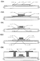
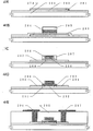
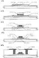
(1) 본 발명은, 비정질 규소막에 규소의 결정화를 조장하는 금속원소를 의도적으로 도입하여, 제 1 의 가열처리에 의해 해당 비정질 규소막을 결정화시켜 결정성 규소막을 얻는 공정과, 산화성 분위기중에서 제 2 의 가열처리를 행하여, 해당 결정성 규소막중에 존재하는 해당 금속원소를 제거 또는 감소시키는 공정과, 해당 공정에서 형성된 열산화막을 제거하는 공정과, 해당 열산화막을 제거한 영역의 표면상에 두번째의 열산화에 의해 열산화막을 형성하는 공정을 갖는 것을 특징으로 하는 반도체 장치의 제작방법을 제공한다.(1) The present invention provides a step of intentionally introducing a metal element that promotes crystallization of silicon into an amorphous silicon film, crystallizing the amorphous silicon film by a first heat treatment to obtain a crystalline silicon film, and A heat treatment of 2 to remove or reduce the metal element present in the crystalline silicon film; a step of removing the thermal oxide film formed in the step; and a second step on the surface of the region from which the thermal oxide film is removed. The manufacturing method of the semiconductor device characterized by having the process of forming a thermal oxidation film by thermal oxidation.
(2) 본 발명은, 비정질 규소막에 규소의 결정화를 조장하는 금속원소를 의도적으로 도입하여, 제 1 의 가열처리에 의해 상기 비정질 규소막을 결정화시켜 결정성 규소막을 얻는 공정과, 산화성 분위기중에서 제 2 의 가열산화처리를 행하여 해당 결정성 규소막의 표면에 열산화막을 형성하여, 해당 열산화막에 해당 금속원소를 게터링시키는 것에 의해 해당 결정성 규소막중에 존재하는 해당 금속원소를 제거 또는 감소시키는 공정과, 해당 공정에서 형성된 열산화막을 제거하는 공정과,해당 열산화막을 제거한 영역의 표면상에 두번째의 열산화에 의해 열산화막을 형성하는 공정을 갖는 것을 특징으로 하는 반도체 장치의 제작방법을 제공한다.(2) The present invention provides a step of intentionally introducing a metal element that promotes crystallization of silicon into an amorphous silicon film, crystallizing the amorphous silicon film by a first heat treatment to obtain a crystalline silicon film, and Performing a heat oxidation treatment of 2 to form a thermal oxide film on the surface of the crystalline silicon film, and gettering the metal element on the thermal oxide film to remove or reduce the metal element present in the crystalline silicon film. And a step of removing the thermal oxide film formed in the step, and a step of forming the thermal oxide film by second thermal oxidation on the surface of the region from which the thermal oxide film is removed. .
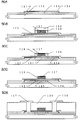
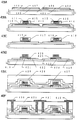
(3) 본 발명은, 비정질 규소막에 규소의 결정화를 조장하는 금속원소를 의도적으로 도입하여, 제 1 의 가열처리에 의해 해당 비정질 규소막을 결정화시켜 결정성 규소막을 얻는 공정과, 산화성 분위기중에서 제 2 의 가열산화처리를 행하여 해당 결정성 규소막중에 존재하는 해당 금속원소를 제거 또는 감소시키는 공정과, 해당 공정에서 형성된 열산화막을 제거하는 공정과, 패터닝을 시행하여 박막트랜지스터의 활성층을 형성하는 공정과, 열산화에 의해 게이트 절연막의 적어도 일부를 구성하는 열산화막을 해당 활성층의 표면에 형성하는 공정을 갖는 것을 특징으로 하는 반도체 장치의 제작방법을 제공한다.(3) The present invention provides a step of intentionally introducing a metal element that promotes crystallization of silicon into an amorphous silicon film, crystallizing the amorphous silicon film by a first heat treatment to obtain a crystalline silicon film, and A process of removing or reducing the metal element present in the crystalline silicon film by performing the heat oxidation treatment of 2, removing the thermal oxide film formed in the process, and forming an active layer of the thin film transistor by patterning. And forming a thermal oxide film constituting at least a part of the gate insulating film by thermal oxidation on the surface of the active layer.
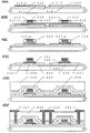
(4) 본 발명은, 비정질 규소막에 규소의 결정화를 조장하는 금속원소를 선택적으로 도입하는 공정과, 제 1 의 가열처리에 의해 해당 금속원소가 선택적으로 도입된 영역에서 막에 평행한 방향으로 결정성장을 행하는 공정과, 산화성 분위기중에서 제 2 의 가열처리를 행하여 해당 결정성장이 행하여진 영역의 표면에 열산화 막을 형성하는 공정과, 해당 열산화막을 제거하는 공정과, 해당 열산화막을 제거한 영역을 사용하여 반도체 장치의 활성층을 형성하는 공정을 갖는 것을 특징으로 하는 반도체 장치의 제작방법을 제공한다.(4) The present invention provides a method of selectively introducing a metal element that promotes crystallization of silicon into an amorphous silicon film, and in a direction parallel to the film in a region where the metal element is selectively introduced by a first heat treatment. A process of performing crystal growth, a second heat treatment in an oxidizing atmosphere to form a thermal oxide film on the surface of the region where the crystal growth is performed, a process of removing the thermal oxide film, and a region from which the thermal oxide film is removed It provides the manufacturing method of the semiconductor device which has a process of forming the active layer of a semiconductor device using.
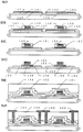
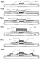
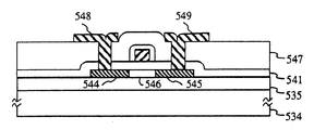
(5) 본 발명은, 제 1 및 제 2 의 산화막에 끼워진 결정성 규소막을 가지며, 해당 제 2 의 산화막상에 게이트 전극을 가지며, 해당 게이트 전극상에 층간절연막을 가지며, 해당 층간절연막에 형성된 콘택트 홀을 통하여, 해당 활성층과 소스 드레인 전극이 접속하고 있으며, 해당 결정성 규소막은 규소의 결정화를 조장하는 금속원소를 함유하고 있으며, 해당 결정성 규소막중에서, 해당 금속원소는 해당 제 1 및/또는 제 2 의 산화막과의 계면근방에서 높은 농도 분포를 가지고 있는 것을 특징으로 하는 반도체 장치를 제공한다.(5) The present invention provides a contact having a crystalline silicon film sandwiched between first and second oxide films, a gate electrode on the second oxide film, an interlayer insulating film on the gate electrode, and a contact formed on the interlayer insulating film. Through the holes, the active layer and the source drain electrode are connected, and the crystalline silicon film contains a metal element that promotes crystallization of silicon, and in the crystalline silicon film, the metal element is the first and / or A semiconductor device having a high concentration distribution in the vicinity of an interface with a second oxide film is provided.
(6) 본 발명은, 산화막으로 이루어지는 기초막과, 해당 기초막상에 형성된 결정성 규소막과, 해당 결정성 규소막상에 형성된 열산화막을 가지며, 해당 열산화막상에 게이트 전극을 가지며, 해당 게이트 전극상에 층간절연막을 가지며, 해당 층간절연막에 형성된 콘택트홀을 통하여, 해당 활성층과 소스· 드레인 전극이 접속하고 있으며, 해당 결정성 규소막중에는 규소의 결정화를 조장하는 금속원소가 포함되고, 해당 규소의 결정화를 조장하는 금속원소는 기초 및/또는 열산화막과의 계면근방에서 높은 농도 분포를 가지며, 해당 열산화막은 박막트랜지스터의 게이트 절연막의 적어도 일부를 구성하는 것을 특징으로 하는 반도체 장치를 제공한다.(6) The present invention has a base film made of an oxide film, a crystalline silicon film formed on the base film, a thermal oxide film formed on the crystalline silicon film, a gate electrode on the thermal oxide film, and a gate electrode. The active layer and the source / drain electrode are connected through a contact hole formed in the interlayer insulating film, and the crystalline silicon film includes a metal element that promotes crystallization of silicon. A metal element that promotes crystallization has a high concentration distribution in the vicinity of an interface with a base and / or a thermal oxide film, and the thermal oxide film constitutes at least a part of a gate insulating film of a thin film transistor.
(7) 본 발명은, 비정질 규소막에 규소의 결정화를 조장하는 금속원소를 의도적으로 도입하여, 제 1 의 가열처리에 의해 해당 비정질 규소막을 결정화시켜 결정성 규소막을 얻는 공정과, 할로겐 원소를 포함한 산화성 분위기중에서 제 2 의 가열처리를 행하여, 해당 결정성 규소막중에 존재하는 해당 금속원소를 제거 또는 감소시키는 공정과, 해당 공정에서 형성된 열산화막을 제거하는 공정과, 해당 열산화막을 제거한 영역의 표면상에 두번째의 열산화에 의해 열산화막을 형성하는 공정을 갖는 것을 특징으로 하는 반도체 장치의 제작방법을 제공한다.(7) The present invention provides a step of intentionally introducing a metal element that promotes crystallization of silicon into an amorphous silicon film, crystallizing the amorphous silicon film by a first heat treatment to obtain a crystalline silicon film, and a halogen element. Performing a second heat treatment in an oxidizing atmosphere to remove or reduce the metal element present in the crystalline silicon film, a step of removing the thermal oxide film formed in the step, and a surface of the region from which the thermal oxide film is removed. There is provided a method of manufacturing a semiconductor device, comprising the step of forming a thermal oxide film by a second thermal oxidation on a phase.
(8) 본 발명은, 비정질 규소막에 규소의 결정화를 조장하는 금속원소를 의도적으로 도입하여, 제 1 의 가열처리에 의해 해당 비정질 규소막을 결정화시켜 결정성 규소막을 얻는 공정과, 할로겐 원소를 포함한 산화성 분위기중에서 제 2 의 가열산화처리를 행하고, 해당 결정성 규소막의 표면에 열산화막을 형성하여, 해당 열산화막에 해당 금속원소를 게터링시키는 것에 의해 해당 결정성 규소막중에 존재하는 해당 금속원소를 제거 또는 감소시키는 공정과, 해당 공정에서 형성된 열산화막을 제거하는 공정과, 해당 열산화막을 제거한 영역의 표면상에 두번째의 열산화에 의해 열산화막을 형성하는 공정을 갖는 것을 특징으로 하는 반도체 장치의 제작방법을 제공한다.(8) The present invention provides a step of intentionally introducing a metal element that promotes crystallization of silicon into an amorphous silicon film, crystallizing the amorphous silicon film by a first heat treatment to obtain a crystalline silicon film, and a halogen element. A second heat oxidation treatment is performed in an oxidizing atmosphere, a thermal oxide film is formed on the surface of the crystalline silicon film, and the metal element is gettered to the thermal oxide film to obtain the metal element present in the crystalline silicon film. And removing or reducing the thermal oxide film formed in the step, and forming a thermal oxide film by a second thermal oxidation on the surface of the region from which the thermal oxide film has been removed. Provide the production method.
(9) 본 발명은, 비정질 규소막에 규소의 결정화를 조장하는 금속원소를 의도적으로 도입하여 제 1 의 가열처리에 의해 해당 비정질 규소막을 결정화시켜 결정성 규소막을 얻는 공정과, 할로겐 원소를 포함한 산화성 분위기중에서 제 2 의 가열산화처리를 행하여 해당 결정성 규소막중에 존재하는 해당 금속원소를 제거 또는 감소시키는 공정과, 해당 공정에서 형성된 열산화막을 제거하는 공정과, 패터닝을 실행하여, 박막트랜지스터의 활성력을 형성하는 공정과, 열산화에 의해 게이트 절연막의 적어도 일부를 구성하는 열산화막을 해당 활성층의 표면에 형성하는 공정을 갖는 것을 특징으로 하는 반도체 장치의 제작방법을 제공한다.(9) The present invention provides a step of intentionally introducing a metal element that promotes crystallization of silicon into an amorphous silicon film, crystallizing the amorphous silicon film by a first heat treatment to obtain a crystalline silicon film, and an oxidizing property including a halogen element. Performing a second heat oxidation treatment in the atmosphere to remove or reduce the metal element present in the crystalline silicon film, a step of removing the thermal oxide film formed in the process, and patterning to activate the thin film transistor. And a step of forming a force and a step of forming a thermal oxide film constituting at least a part of the gate insulating film by thermal oxidation on the surface of the active layer.
(10) 본 발명은, 비정질 규소막에 규소의 결정화를 조장하는 금속원소를 선택적으로 도입하는 공정과, 제 1 의 가열처리에 의해 해당 금속원소가 선택적으로 도입된 영역에서 막에 평행한 방향으로 결정성장을 행하게 하는 공정과, 할로겐 원소를 포함한 산화성 분위기중에서 제 2 의 가열처리를 행하여, 해당 결정성장이 행하여진 영역의 표면에 열산화막을 형성하는 공정과, 해당 열산화막을 제거하는 공정과, 해당 열산화막을 제거한 영역을 사용하여 반도체 장치의 활성층을 형성하는 공정을 갖는 것을 특징으로 하는 반도체 장치의 제작방법을 제공한다.(10) The present invention provides a process for selectively introducing a metal element that promotes crystallization of silicon into an amorphous silicon film, and in a direction parallel to the film in a region where the metal element is selectively introduced by a first heat treatment. A process of causing crystal growth, a second heat treatment in an oxidizing atmosphere containing a halogen element to form a thermal oxide film on the surface of the region where the crystal growth is performed, a process of removing the thermal oxide film, The manufacturing method of the semiconductor device characterized by having the process of forming the active layer of a semiconductor device using the area | region which removed this thermal oxidation film.
(11) 본 발명은, 제 1 및 제 2 의 산화막에 끼워진 결정성 규소막을 가지며, 해당 제 2 의 산화막상에 게이트 전극을 가지며, 해당 게이트 전극상에 층간절연막을 가지며, 해당 층간절연막에 형성된 콘택트홀을 통하여, 해당 활성층과 소스· 드레인 전극이 접속하고 있으며, 해당 결정성 규소막은 수소 및 할로겐 원소를 포함하며, 또한 규소의 결정화를 조장하는 금속원소를 함유하고 있으며, 해당 결정성 규소막중에서, 해당 금속원소는 해당 제 1 및/또는 제 2 의 산화막과의 계면근방에서 높은 농도 분포를 가지고 있는 것을 특징으로 하는 반도체 장치를 제공한다.(11) The present invention provides a contact having a crystalline silicon film sandwiched between first and second oxide films, a gate electrode on the second oxide film, an interlayer insulating film on the gate electrode, and a contact formed on the interlayer insulating film. Through the holes, the active layer and the source / drain electrode are connected, the crystalline silicon film contains hydrogen and a halogen element, and contains a metal element that promotes crystallization of silicon, and in the crystalline silicon film, The metal element has a high concentration distribution in the vicinity of the interface with the first and / or second oxide film.
(12) 본 발명은, 산화막으로 이루어지는 기초막과, 해당 기초막상에 형성된 결정성 규소막과, 해당 결정성 규소막상에 형성된 열산화막을 가지며, 해당 열산화막상에 게이트 전극을 가지며, 해당 게이트 전극상에 층간절연막을 가지며, 해당 층간절연막에 형성된 콘택트홀을 통하여, 해당 활성층과 소스· 드레인 전극이 접속하고 있으며, 해당 결정성 규소막중에는 규소의 결정화를 조장하는 금속원소 및 수소 및 할로겐 원소가 포함되고, 해당 규소의 결정화를 조장하는 금속원소는 기초막 및/또는 열산화막과의 계면근방에서 높은 농도 분포를 가지며, 해당 열산화막이 박막트랜지스터의 게이트 절연막의 적어도 일부를 구성하는 것을 특징으로 하는 반도체 장치를 제공한다.(12) The present invention has a base film made of an oxide film, a crystalline silicon film formed on the base film, a thermal oxide film formed on the crystalline silicon film, a gate electrode on the thermal oxide film, and a gate electrode. The active layer and the source / drain electrode are connected to each other through a contact hole formed in the interlayer insulating film, and the crystalline silicon film contains a metal element which promotes crystallization of silicon, hydrogen and a halogen element. The metal element which promotes crystallization of the silicon has a high concentration distribution near the interface with the base film and / or the thermal oxide film, and the thermal oxide film constitutes at least part of the gate insulating film of the thin film transistor. Provide the device.
(13) 본 발명은, 비정질 규소막에 규소의 결정화를 조장하는 금속원소를 의도적으로 도입하여, 제 1 의 가열처리에 의해 해당 비정질 규소막을 결정화시켜 결정성 규소막을 얻는 공정과, 해당 결정성 규소막에 대하여 레이저광 또는 강광의 조사를 행하는 공정과, 할로겐 원소를 포함한 산화성 분위기중에서 제 2 의 가열처리를 행하여 해당 결정성 규소막중에 존재하는 해당 금속원소를 제거 또는 감소시키는 공정과, 해당 공정에서 형성된 열산화막을 제거하는 공정과, 해당 열산화막을 제거한 영역의 표면상에 두번째의 열산화에 의해 열산화막을 형성하는 공정을 갖는 것을 특징으로 하는 반도체 장치의 제작방법을 제공한다.(13) The present invention provides a step of intentionally introducing a metal element that promotes crystallization of silicon into an amorphous silicon film, crystallizing the amorphous silicon film by a first heat treatment to obtain a crystalline silicon film, and the crystalline silicon Irradiating a laser beam or a strong light to the film; and performing a second heat treatment in an oxidizing atmosphere containing a halogen element to remove or reduce the metal element present in the crystalline silicon film. And a step of forming a thermal oxide film by a second thermal oxidation on a surface of a region from which the thermal oxide film is removed.
(14) 본 발명은, 비정질 규소막에 규소의 결정화를 조장하는 금속원소를 의도적으로 도입하여 제 1 의 가열처리에 의해 해당 비정질 규소막을 결정화시켜 결정성 규소막을 얻는 공정과, 해당 결정성 규소막에 대하여 레이저광 또는 강광의 조사를 행하여 해당 결정성 규소막중에 존재하는 해당 금속원소를 해당 결정성 규소막중에 있어서 확산시키는 공정과, 할로겐 원소를 포함한 산화성 분위기중에서 제 2 의 가열처리를 행하여 해당 결정성 규소막중에 존재하는 해당 금속원소를 형성되는 열산화막중에 게터링하는 공정과, 해당 공정에서 형성된 열산화막을 제거하는 공정과, 해당 열산화막을 제거한 영역의 표면상에 두번째의 열산화에 의해 열산화막을 형성하는 공정을 갖는 것을 특징으로 하는 반도체 장치의 제작방법을 제공한다.(14) The present invention provides a step of intentionally introducing a metal element that promotes crystallization of silicon into an amorphous silicon film, crystallizing the amorphous silicon film by a first heat treatment to obtain a crystalline silicon film, and the crystalline silicon film Irradiating laser light or strong light to diffuse the metal element present in the crystalline silicon film in the crystalline silicon film, and performing a second heat treatment in an oxidizing atmosphere containing a halogen element to determine the crystal. A process of getting gettered in the thermally oxidized film forming the metal element present in the silicon silicon film, removing the thermal oxidized film formed in the process, and heat by second thermal oxidation on the surface of the region where the thermal oxidized film is removed. Provided is a method for manufacturing a semiconductor device, comprising the step of forming an oxide film.
(15) 본 발명은, 비정질 규소막에 규소의 결정화를 조장하는 금속원소를 의도적 또한 선택적으로 도입하는 공정과, 해당 비정질 규소막에 대하여 제 1 의 가열처리를 시행하여, 해당 의도적이고 또한 선택적으로 금속원소가 도입된 영역에서막에 평행한 방향으로 결정성장을 행하게 하는 공정과, 레이저광 또는 강광의 조사를 행하여 해당 결정성장한 영역중에 존재하는 해당 금속원소를 확산시키는 공정과, 할로겐 원소를 포함한 산화성 분위기중에서 제 2 의 가열처리를 행하여 해당 결정성장한 영역에 존재하는 해당 금속원소를, 형성되는 열산화막중에 게터링하는 공정과, 해당 공정에서 형성된 열산화막을 제거하는 공정과, 해당 열산화막을 제거한 영역의 표면상에 두번째의 열산화에 의해 열산화막을 형성하는 공정을 갖는 것을 특징으로 하는 반도체 장치의 제작방법을 제공한다.(15) The present invention provides a step of intentionally and selectively introducing a metal element that promotes crystallization of silicon into an amorphous silicon film, and performing a first heat treatment on the amorphous silicon film, thereby intentionally and selectively A process of causing crystal growth in a direction parallel to the film in a region where the metal element is introduced, a process of diffusing the metal element existing in the crystal grown region by irradiation of laser light or strong light, and an oxidative property including a halogen element Performing a second heat treatment in the atmosphere to getter the metal element present in the crystal grown region in the thermal oxide film formed, removing the thermal oxide film formed in the process, and removing the thermal oxide film. Having a process of forming a thermal oxide film by a second thermal oxidation on the surface of It provides a production method of the apparatus body.
(16) 본 발명은, 비정질 규소막에 규소의 결정화를 조장하는 금속원소를 의도적으로 도입하여 제 1 의 가열처리에 의해 해당 비정질 규소막을 결정화시켜 결정성 규소막을 얻는 공정과, 해당 결정성 규소막을 패터닝하여 반도체 장치의 활성 층을 형성하는 공정과, 해당 활성층에 대하여 레이저광 또는 강광의 조사를 행하는 공정과, 할로겐 원소를 포함한 산화성 분위기중에서 제 2 의 가열처리를 행하여 해당 활성층중에 존재하는 해당 금속원소를 제거 또는 감소시키는 공정과, 해당 공정에서 형성된 열산화막을 제거하는 공정과, 해당 활성층의 표면에 두번째의 열산화에 의해 열산화막을 형성하는 공정을 갖는 것을 특징으로 하는 반도체 장치의 제작 방법을 제공한다.(16) The present invention provides a step of intentionally introducing a metal element that promotes crystallization of silicon into an amorphous silicon film, crystallizing the amorphous silicon film by a first heat treatment to obtain a crystalline silicon film, and the crystalline silicon film. Patterning the active layer of the semiconductor device by patterning, irradiating a laser light or a strong light to the active layer, and performing a second heat treatment in an oxidizing atmosphere containing a halogen element to form the metal element present in the active layer. And removing the thermal oxide film formed in the process, and forming a thermal oxide film on the surface of the active layer by a second thermal oxidation. do.
(17) 본 발명은, 비정질 규소막에 규소의 결정화를 조장하는 금속원소를 의도적으로 도입하여 제 1 의 가열처리에 의해 해당 비정질 규소막을 결정화시켜 결정성 규소막을 얻는 공정과, 해당 결정성 규소막을 패터닝하여 반도체 장치의 활성 층을 형성하는 공정과, 해당 활성층에 대하여 레이저광 또는 강광의 조사를 행하는공정과, 할로겐 원소를 포함한 산화성 분위기중에서 제 2 의 가열처리를 행하여 해당 활성층중에 존재하는 해당 금속원소를 제거 또는 감소시키는 공정과, 해당 공정에서 형성된 열산화막을 제거하는 공정과, 해당 활성층의 표면에 두번째의 열산화에 의해 열산화막을 형성하는 공정을 가지며, 해당 활성층은 측면이 기초면과의 이루는 각이 20° 내지 50° 를 가지는 경사된 형상을 가지는 것을 특징으로 하는 반도체 장치의 제작방법을 제공한다.(17) The present invention provides a process for obtaining a crystalline silicon film by intentionally introducing a metal element that promotes crystallization of silicon into an amorphous silicon film and crystallizing the amorphous silicon film by a first heat treatment, and the crystalline silicon film Patterning the active layer of the semiconductor device by patterning, irradiating a laser beam or a strong light to the active layer, and performing a second heat treatment in an oxidizing atmosphere containing a halogen element to form the metal element present in the active layer. And a process of removing the thermal oxide film formed in the process, and forming a thermal oxide film on the surface of the active layer by the second thermal oxidation. Method of manufacturing a semiconductor device, characterized in that having an inclined shape having an angle of 20 ° to 50 ° Provided.
(18) 본 발명은, 비정질 규소막에 규소의 결정화를 조장하는 금속원소를 의도적으로 도입하여 제 1 의 가열처리에 의해 해당 비정질 규소막을 결정화시켜 결정성 규소막을 얻는 공정과, 해당 결정성 규소막에 대하여 레이저광 또는 강광의 조사를 행하는 공정과, 산화성 분위기중에서 제 2 의 가열처리를 행하여 해당 결정성 규소막중에 존재하는 해당 금속원소를 제거 또는 감소시키는 공정과, 해당 공정에서 형성된 열산화막을 제거하는 공정과, 해당 열산화막을 제거한 영역의 표면상에 두번째의 열산화에 의해 열산화막을 형성하는 공정을 갖는 것을 특징으로 하는 반도체 장치의 제작방법을 제공한다.(18) The present invention provides a step of intentionally introducing a metal element that promotes crystallization of silicon into an amorphous silicon film, crystallizing the amorphous silicon film by a first heat treatment to obtain a crystalline silicon film, and the crystalline silicon film Irradiating the laser light or the strong light with respect to the light, performing a second heat treatment in an oxidizing atmosphere to remove or reduce the metal element present in the crystalline silicon film, and removing the thermal oxide film formed in the process. And a step of forming a thermal oxide film by second thermal oxidation on the surface of the region from which the thermal oxide film is removed.
(19) 본 발명은, 비정질 규소막에 규소의 결정화를 조장하는 금속원소를 의도적으로 도입하여 제 1 의 가열처리에 의해 해당 비정질 규소막을 결정화시켜 결정성 규소막을 얻는 공정과, 해당 결정성 규소막에 대하여 레이저광 또는 강광의 조사를 행하여 해당 결정성 규소막중에 존재하는 해당 금속원소를 해당 결정성 규소막중에 있어서 확산시키는 공정과, 산화성 분위기중에서 제 2 의 가열처리를 행하여, 해당 결정성 규소막중에 존재하는 해당 금속원소를, 형성되는 열산화막중에게터링하는 공정과, 해당 공정에서 형성된 열산화막을 제거하는 공정과, 해당 열산화막을 제거한 영역의 표면상에 두번째의 열산화에 의해 열산화막을 형성하는 공정을 갖는 것을 특징으로 하는 반도체 장치의 제작방법을 제공한다.(19) The present invention provides a step of intentionally introducing a metal element that promotes crystallization of silicon into an amorphous silicon film, crystallizing the amorphous silicon film by a first heat treatment to obtain a crystalline silicon film, and the crystalline silicon film Irradiating the laser light or the strong light with respect to the metal element present in the crystalline silicon film and diffusing the crystalline silicon film in the crystalline silicon film, and performing a second heat treatment in an oxidative atmosphere, A thermal oxidation film is formed by subjecting the metal element present in the thermal oxide film to the formed thermal oxide film, removing the thermal oxide film formed in the process, and second thermal oxidation on the surface of the region from which the thermal oxide film is removed. It provides a manufacturing method of a semiconductor device having a step of forming.
(20) 본 발명은, 비정질 규소막에 규소의 결정화를 조장하는 금속원소를 의도적 또한 선택적으로 도입하는 공정과, 해당 비정질 규소막에 대하여 제 1 의 가열처리를 시행하여, 해당 의도적이고 또한 선택적으로 금속원소가 도입된 영역에서 막에 평행한 방향으로 결정성장을 행하게 하는 공정과, 레이저광 또는 강광의 조사를 행하여 해당 결정성장한 영역중에 존재하는 해당 금속원소를 확산시키는 공정과, 산화성 분위기중에서 제 2 의 가열처리를 행하여, 해당 결정성장한 영역에 존재하는 해당 금속원소를, 형성되는 열산화막중에 게터링하는 공정과, 해당 공정에서 형성된 열산화막을 제거하는 공정과, 해당 열산화막을 제거한 영역의 표면상에 두번째의 열산화에 의해 열산화막을 형성하는 공정을 갖는 것을 특징으로 하는 반도체 장치의 제작방법을 제공한다.(20) The present invention provides a step of intentionally and selectively introducing a metal element that promotes crystallization of silicon into an amorphous silicon film, and performing a first heat treatment on the amorphous silicon film, thereby intentionally and selectively Performing crystal growth in a direction parallel to the film in the region where the metal element is introduced; irradiating laser light or strong light to diffuse the metal element present in the crystal growth region; and second in an oxidizing atmosphere. Performing a heat treatment to getter the metal element present in the crystal-grown region in the thermal oxide film formed, removing the thermal oxide film formed in the step, and removing the thermal oxide film on the surface of the region from which the thermal oxide film is removed. And a step of forming a thermal oxide film by second thermal oxidation. Provided.
(21) 본 발명은, 비정질 규소막에 규소의 결정화를 조장하는 금속원소를 의도적으로 도입하여 제 1 의 가열처리에 의해 해당 비정질 규소막을 결정화시켜 결정성 규소막을 얻는 공정과, 해당 결정성 규소막을 패터닝하여 반도체 장치의 활성 층을 형성하는 공정과, 해당 활성층에 대하여 레이저광 또는 강광의 조사를 행하는 공정과, 산화성 분위기중에서 제 2 의 가열처리를 행하여 해당 활성층중에 존재하는 해당 금속원소를 제거 또는 감소시키는 공정과, 해당 공정에서 형성된 열산화막을 제거하는 공정과, 해당 활성층의 표면에 두번째의 열산화에 의해 열산화막을 형성하는 공정을 갖는 것을 특징으로 하는 반도체 장치의 제작방법을 제공한다.(21) The present invention provides a process for obtaining a crystalline silicon film by intentionally introducing a metal element that promotes crystallization of silicon into an amorphous silicon film and crystallizing the amorphous silicon film by a first heat treatment, and the crystalline silicon film Patterning to form the active layer of the semiconductor device, irradiating laser light or strong light to the active layer, and performing a second heat treatment in an oxidizing atmosphere to remove or reduce the metal element present in the active layer. And a step of removing the thermal oxide film formed in the step, and a step of forming the thermal oxide film on the surface of the active layer by second thermal oxidation.
(22) 본 발명은, 비정질 규소막에 규소의 결정화를 조장하는 금속원소를 의도적으로 도입하여 제 1 의 가열처리에 의해 해당 비정질 규소막을 결정화시켜 결정성 규소막을 얻는 공정과, 해당 결정성 규소막을 패터닝하여 반도체 장치의 활성 층을 형성하는 공정과, 해당 활성층에 대하여 레이저광 또는 강광의 조사를 행하는 공정과, 산화성 분위기중에서 제 2 의 가열처리를 행하여 해당 활성층중에 존재하는 해당 금속원소를 제거 또는 감소시키는 공정과, 해당 공정에서 형성된 열산화막을 제거하는 공정과, 해당 활성층의 표면에 두번째의 열산화에 의해 열산화막을 형성하는 공정을 가지며, 해당 활성층은 측면이 기초면과의 이루는 각이 20° 내지 50° 를 가지는 경사진 형상을 가지는 것을 특징으로 하는 반도체 장치의 제작방법을 제공한다.(22) The present invention provides a process for obtaining a crystalline silicon film by intentionally introducing a metal element that promotes crystallization of silicon into an amorphous silicon film and crystallizing the amorphous silicon film by a first heat treatment, and the crystalline silicon film Patterning to form the active layer of the semiconductor device, irradiating laser light or strong light to the active layer, and performing a second heat treatment in an oxidizing atmosphere to remove or reduce the metal element present in the active layer. And a step of removing a thermal oxide film formed in the step, and a step of forming a thermal oxide film on the surface of the active layer by a second thermal oxidation. It provides a method for manufacturing a semiconductor device, characterized in that it has an inclined shape having a 50 to 50 degrees.
(23) 본 발명은 절연표면을 가지는 기판상에 비정질 규소막을 성막하는 공정과, 해당 비정질 규소막에 규소의 결정화를 조장하는 금속원소를 의도적으로 도입하는 공정과, 온도 750℃ 내지 1100℃의 제 1 의 가열처리에 의해 해당 비정질 규소막을 결정화시켜 결정성 규소막을 얻는 공정과, 해당 결정성 규소막을 패터닝하여 반도체 장치의 활성층을 형성하는 공정과, 할로겐 원소를 포함한 산화성 분위기 중에서 제 2 의 가열처리를 행하여 해당 활성층중에 존재하는 해당 금속원소를 제거 또는 감소시키는 공정과, 해당 공정에서 형성된 열산화막을 제거하는 공정과, 해당 열산화막을 제거한 후에 두번째의 열산화에 의해 열산화막을 형성하는 공정을 가지며, 해당 제 2 의 가열처리의 온도는 해당 제 1 의 가열처리의 온도보다도 높은 것을 특징으로 하는 반도체 장치의 제작방법을 제공한다.(23) The present invention provides a process for forming an amorphous silicon film on a substrate having an insulating surface, a step of intentionally introducing a metal element that promotes crystallization of silicon into the amorphous silicon film, and a temperature of 750 ° C to 1100 ° C. A process of obtaining a crystalline silicon film by crystallizing the amorphous silicon film by the heat treatment of 1, patterning the crystalline silicon film to form an active layer of a semiconductor device, and performing a second heat treatment in an oxidizing atmosphere containing a halogen element. And removing or reducing the metal element present in the active layer, removing the thermal oxide film formed in the step, and removing the thermal oxide film to form the thermal oxide film by second thermal oxidation. The temperature of the second heat treatment is higher than the temperature of the first heat treatment. Provided is a method of manufacturing a conductor device.
(24) 본 발명은 절연표면을 가지는 기판상에 비정질 규소막을 성막하는 공정과, 해당 비정질 규소막에 규소의 결정화를 조장하는 금속원소를 의도적으로 도입하는 공정과, 온도 750℃ 내지 1100℃의 제 1 의 가열처리에 의해 해당 비정질 규소막을 결정화시켜 결정성 규소막을 얻는 공정과, 해당 결정성 규소막을 패터닝하여 반도체 장치의 활성층을 형성하는 공정과, 할로겐 원소를 포함한 산화성 분위기 중에서 제 2 의 가열처리를 행하여, 해당 활성층중에 존재하는 해당 금속원소를, 형성되는 열산화막중에 게터링시키는 공정과, 해당 공정에서 형성된 열산화막을 제거하는 공정과, 해당 열산화막을 제거한 후에 두번째의 열산화에 의해 열산화막을 형성하는 공정을 가지며, 해당 제 2 의 가열처리의 온도는 해당 제 1 의 가열처리의 온도보다도 높은 것을 특징으로 하는 반도체 장치의 제작방법을 제공한다.(24) The present invention provides a process for forming an amorphous silicon film on a substrate having an insulating surface, a step of intentionally introducing a metal element that promotes crystallization of silicon into the amorphous silicon film, and a temperature of 750 ° C to 1100 ° C. A process of obtaining a crystalline silicon film by crystallizing the amorphous silicon film by the heat treatment of 1, patterning the crystalline silicon film to form an active layer of a semiconductor device, and performing a second heat treatment in an oxidizing atmosphere containing a halogen element. Performing a gettering of the metal element present in the active layer in the thermal oxide film formed; removing the thermal oxide film formed in the step; and removing the thermal oxide film, and then removing the thermal oxide film by a second thermal oxidation. It has a process of forming and the temperature of the said 2nd heat processing is higher than the temperature of the said 1st heat processing. A method of manufacturing a semiconductor device is provided.
(25) 본 발명은 절연표면을 가지는 기판상에 비정질 규소막을 성막하는 공정과, 해당 비정질 규소막에 규소의 결정화를 조장하는 금속원소를 의도적 또한 선택적으로 도입하는 공정과, 온도 750℃ 내지 1100℃의 제 1 의 가열처리에 의해 해당 비정질 규소막의 해당 금속원소가 의도적 또한 선택적으로 도입된 영역에서 막에 평행한 방향으로 결정성장을 행하게 하는 공정과, 패터닝을 행하여 해당 막에 평행한 방향으로 결정성장한 영역을 사용하여 반도체 장치의 활성층을 형성하는 공정과, 할로겐 원소를 포함한 산화성 분위기중에서 제 2 의 가열처리를 행하여 해당 활성층중에 존재하는 해당 금속원소를 형성되는 열산화막중에 게터링시키는 공정과, 해당 공정에서 형성된 열산화막을 제거하는 공정과, 해당 열산화막을 제거한후에 두번째의 열산화에 의해 열산화막을 형성하는 공정을 가지며, 해당 제 2 의 가열처리의 온도는 해당 제 1 의 가열처리의 온도보다도 높은 것을 특징으로 하는 반도체 장치의 제작방법을 제공한다.(25) The present invention provides a step of forming an amorphous silicon film on a substrate having an insulating surface, a step of intentionally and selectively introducing a metal element that promotes crystallization of silicon into the amorphous silicon film, and a temperature of 750 ° C to 1100 ° C. Causing crystal growth in a direction parallel to the film in a region in which the metal element of the amorphous silicon film is intentionally and selectively introduced by the first heat treatment of the film, and patterning to crystal growth in a direction parallel to the film. Using a region to form an active layer of a semiconductor device, performing a second heat treatment in an oxidizing atmosphere containing a halogen element, and gettering the thermally oxidized film to form the metal element present in the active layer; Removing the thermal oxide film formed at the step of Has a step of forming an oxide film by heat, the temperature of the second heat treatment provides a manufacturing method of a semiconductor device, characterized in that is higher than the temperature of the heat treatment of the first.
(26) 본 발명은, 비정질 규소막을 형성하는 공정과, 해당 비정질 규소막의 표면에 규소의 결정화를 조장하는 금속원소를 접하여 유지시키는 공정과, 제 1 의 가열처리를 행하여 해당 비정질 규소막을 결정화시켜 결정성 규소막을 얻는 공정과, 산소와 수소와 플루오르를 포함하는 분위기중에 있어서 온도 500℃ 내지 700℃에서의 제 2 의 가열처리를 행하여 해당 결정성 규소막의 표면에 열산화막을 형성하는 공정과, 해당 열산화막을 제거하는 공정을 갖는 것을 특징으로 하는 반도체 장치의 제작방법을 제공한다.(26) The present invention provides a step of forming an amorphous silicon film, a step of contacting and maintaining a metal element that promotes crystallization of silicon on the surface of the amorphous silicon film, and performing a first heat treatment to crystallize the amorphous silicon film to crystallize it. A step of obtaining a silicon oxide film, a second heat treatment at a temperature of 500 ° C. to 700 ° C. in an atmosphere containing oxygen, hydrogen, and fluorine to form a thermal oxide film on the surface of the crystalline silicon film; Provided is a method of manufacturing a semiconductor device, comprising the step of removing an oxide film.
(27) 본 발명은, 비정질 규소막을 형성하는 공정과, 해당 비정질 규소막의 표면에 규소와 결정화를 조장하는 금속원소를 접하여 유지시키는 공정과, 제 1 의 가열처리를 행하여 해당 비정질 규소막을 결정화시켜 결정성 규소막을 얻는 공정과, 산소와 수소와 플루오르와 염소를 포함하는 분위기중에 있어서 온도 500℃ 내지 700℃에서의 제 2 의 가열처리를 행하여 해당 결정성 규소막의 표면에 열산화막을 형성하는 공정과, 해당 열산화막을 제거하는 공정을 갖는 것을 특징으로 하는 반도체 장치의 제작방법을 제공한다.(27) The present invention provides a step of forming an amorphous silicon film, a step of contacting and maintaining silicon and a metal element that promotes crystallization on the surface of the amorphous silicon film, and performing a first heat treatment to crystallize the amorphous silicon film to crystallize it. A step of obtaining a silicon oxide film, a second heat treatment at a temperature of 500 ° C. to 700 ° C. in an atmosphere containing oxygen, hydrogen, fluorine, and chlorine to form a thermal oxide film on the surface of the crystalline silicon film; There is provided a method of manufacturing a semiconductor device, the method comprising the step of removing the thermal oxide film.
(28) 본 발명은, 비정질 규소막을 형성하는 공정과, 해당 비정질 규소막의 표면에 규소의 결정화를 조장하는 금속원소를 접하여 유지시키는 공정과, 가열처리를 행하여 해당 비정질 규소막을 결정화시켜 결정성 규소막을 얻는 공정과, 플루오르 및/또는 염소를 포함하는 분위기중에 있어서 웨트산화막을 상기 결정성 규소막의 표면에 형성하는 공정과, 해당 산화막을 제거하는 공정을 갖는 것을 특징으로 하는 반도체 장치의 제작방법을 제공한다.(28) The present invention provides a step of forming an amorphous silicon film, a step of contacting and maintaining a metal element that promotes crystallization of silicon on the surface of the amorphous silicon film, and heat treatment to crystallize the amorphous silicon film to form a crystalline silicon film. And a step of forming a wet oxide film on the surface of the crystalline silicon film in an atmosphere containing fluorine and / or chlorine, and a step of removing the oxide film. .
(29) 본 발명은, 결정성을 가지는 규소막을 가지는 반도체 장치로서, 해당 규소막상에 게이트 절연막을 가지며, 해당 게이트 절연막상에 게이트 전극을 가지며, 해당 게이트 전극상에 층간절연막을 가지며, 해당 층간절연막에 형성된 콘택트 홀을 통하여, 해당 규소막과 소스· 드레인 전극이 접속하고 있으며, 해당 규소막에는 규소의 결정화를 조장하는 금속원소가 1 x 1016cm-3내지 5 x 1018cm-3의 농도로 포함되고, 플루오르 원자가 1 x 1015cm-3내지 1 x 1020cm-3의 농도로 포함되고, 수소원자가 1 x 1017cm-3내지 1 x 1021cm-3의 농도로 포함되어 있는 것을 특징으로 하는 반도체 장치를 제공한다. 또한, 농도단위 「‥‥ cm-3」은 1 입방 센티미터 당 원자수(atoms/cm3)를 의미하고, 이 점, 본 명세서중에서 동일하다.(29) The present invention is a semiconductor device having a silicon film having crystallinity, comprising: a gate insulating film on the silicon film, a gate electrode on the gate insulating film, an interlayer insulating film on the gate electrode, and an interlayer insulating film. The silicon film and the source / drain electrode are connected to each other via a contact hole formed in the silicon film, and the silicon film has a concentration of 1 x 10 16 cm -3 to 5 x 10 18 cm -3 that promotes crystallization of silicon. Fluorine atoms in a concentration of 1 x 10 15 cm -3 to 1 x 10 20 cm -3 and hydrogen atoms in a concentration of 1 x 10 17 cm -3 to 1 x 10 21 cm -3 A semiconductor device is provided. In addition, the concentration unit "... cm -3 " means the number of atoms (atoms / cm <3> ) per cubic centimeter, and this is the same in this specification.
(30) 본 발명은, 비정질 규소막을 형성하는 공정과, 해당 비정질 규소막을 결정화하여 결정성 규소막을 형성하는 공정과, 플루오르 화합물 기체가 첨가된 산화성 분위기중에서 가열하여, 해당 결정성 규소막의 표면에 열산화막을 성장시키는 공정과, 해당 결정성 규소막 표면의 열산화막을 제거하는 공정과, 해당 결정성 규소막의 표면에 절연막을 퇴적하는 공정을 갖는 것을 특징으로 하는 반도체 장치의 제작방법을 제공한다.(30) The present invention provides a process of forming an amorphous silicon film, a process of crystallizing the amorphous silicon film to form a crystalline silicon film, and heating in an oxidizing atmosphere to which a fluorine compound gas is added, thereby heating the surface of the crystalline silicon film. A method of manufacturing a semiconductor device comprising the steps of growing an oxide film, removing a thermal oxide film on the surface of the crystalline silicon film, and depositing an insulating film on the surface of the crystalline silicon film.
(31) 본 발명은, 비정질 규소막을 형성하는 공정과, 레이저광을 조사하여 해당 비정질 규소막을 결정화하여 결정성 규소막을 형성하는 공정과, 플루오르 화합물 기체가 첨가된 산화성 분위기중에서 가열하여 해당 결정성 규소막의 표면에 열산화막을 성장시키는 공정과, 해당 결정성 규소막 표면의 열산화막을 제거하는 공정과, 해당 결정성 규소막의 표면에 절연막을 퇴적하는 공정을 갖는 것을 특징으로 하는 반도체 장치의 제작방법을 제공한다.(31) The present invention provides a process for forming an amorphous silicon film, a process of irradiating a laser beam to crystallize the amorphous silicon film to form a crystalline silicon film, and heating in an oxidizing atmosphere to which a fluorine compound gas is added to the crystalline silicon. A method of manufacturing a semiconductor device comprising the steps of growing a thermal oxide film on the surface of the film, removing the thermal oxide film on the surface of the crystalline silicon film, and depositing an insulating film on the surface of the crystalline silicon film. to provide.
(32) 본 발명은, 절연표면을 가지는 기판상에 박막트랜지스터를 제작하는 방법에 있어서, 비정질 규소막을 형성하는 공정과, 해당 비정질 규소막을 결정화하여 결정성 규소막을 형성하는 공정과, 플루오르 화합물 기체가 첨가된 산화성 분위기 중에서 가열하여, 해당 결정성 규소막의 표면에 열산화막을 성장시키는 공정과, 해당 결정성 규소막 표면의 열산화막을 제거하는 공정과, 해당 결정성 규소막을 정형하여 박막트랜지스터의 활성층을 형성하는 공정과, 해당 활성력의 표면에 절연막을 퇴적하여, 적어도 채널영역의 표면에 게이트 절연막을 형성하는 공정과, 해당 게이트 절연막의 표면에 게이트 전극을 형성하는 공정과, 해당 게이트 전극을 마스크로하여 해당 활성층에 전도형을 부여하는 불순물 이온을 주입하고, 소스, 드레인을 자기 정합적으로 형성하는 공정을 갖는 것을 특징으로 하는 반도체 장치의 제작방법을 제공한다.(32) The present invention provides a method of manufacturing a thin film transistor on a substrate having an insulating surface, the method comprising forming an amorphous silicon film, crystallizing the amorphous silicon film to form a crystalline silicon film, and a fluorine compound gas Heating the added oxidizing atmosphere to grow a thermal oxide film on the surface of the crystalline silicon film, removing the thermal oxide film on the surface of the crystalline silicon film, and shaping the crystalline silicon film to form an active layer of the thin film transistor. Forming a gate insulating film on at least the surface of the channel region; forming a gate electrode on the surface of the gate insulating film; forming a gate electrode on the surface of the gate insulating film; Injecting impurity ions imparting conductivity to the active layer and self-aligning the source and drain It provides a manufacturing method of a semiconductor device, characterized by having a step of forming a.
(33) 본 발명은, 절연표면을 가지는 기판상에 박막트랜지스터를 제작하는 방법에 있어서, 비정질 규소막을 형성하는 공정과, 해당 비정질 규소막을 결정화하여 결정성 규소막을 형성하는 공정과, 해당 결정성 규소막에 레이저광을 조사하는 공정과, 플루오르 화합물 기체가 첨가된 산화성 분위기중에서 가열하여 해당 결정성 규소막의 표면에 열산화막을 성장시키는 공정과, 해당 결정성 규소막 표면의 열산화막을 제거하는 공정과, 해당 결정성 규소막을 정형하여, 박막트랜지스터의 활성 층을 형성하는 공정과, 해당 활성층의 표면에 절연막을 퇴적하여 적어도 채널영역의 표면에 게이트 절연막을 형성하는 공정과, 해당 게이트 절연막의 표면에 게이트 전극을 형성하는 공정과, 해당 게이트 전극을 마스크로 하여 해당 활성층에 전도형을 부여하는 불순물 이온을 주입하여, 소스, 드레인을 자기 정합적으로 형성하는 공정을 갖는 것을 특징으로 하는 반도체 장치의 제작방법을 제공하는 것이다.(33) The present invention provides a method of fabricating a thin film transistor on a substrate having an insulating surface, the method comprising forming an amorphous silicon film, crystallizing the amorphous silicon film to form a crystalline silicon film, and the crystalline silicon Irradiating a laser beam to the film, heating in an oxidizing atmosphere to which a fluorine compound gas is added, growing a thermal oxide film on the surface of the crystalline silicon film, removing a thermal oxide film on the surface of the crystalline silicon film; Forming a crystalline silicon film to form an active layer of the thin film transistor; depositing an insulating film on the surface of the active layer to form a gate insulating film on at least the surface of the channel region; A process of forming an electrode, and a fire for imparting conductivity to the active layer using the gate electrode as a mask Implanting ions of water, to provide a manufacturing method of a semiconductor device characterized by having a step of forming a source and drain in a self-aligning manner.
도 1은 본 발명에 의해서 얻어진 결정성 규소막의 미세구조를 나타내는 도면(광학현미경 사진: 450 배).1 is a view showing the microstructure of a crystalline silicon film obtained by the present invention (optical micrograph: 450 times).
도 2는 본 발명에 의해서 얻어진 결정성 규소막의 미세구조를 나타내는 도면(광학현미경 사진: 450 배).Fig. 2 is a view showing the microstructure of the crystalline silicon film obtained by the present invention (optical micrograph: 450 times).
도 3은 본 발명에 의해서 얻어진 결정성 규소막의 미세구조를 나타내는 도면(TEM: 50000 배).Fig. 3 is a view showing the microstructure of the crystalline silicon film obtained by the present invention (TEM: 50000 times).
도 4는 본 발명에 의해서 얻어진 결정성 규소막의 미세구조를 나타내는 도면(TEM: 250000배).Fig. 4 is a diagram showing the microstructure of the crystalline silicon film obtained by the present invention (TEM: 250000 times).
도 5A 내지 5G는 본 발명과 관계되는 결정성 규소막의 제작공정의 전형적인 예를 나타내는 도면.5A to 5G show typical examples of the steps for producing the crystalline silicon film according to the present invention.
도 6G 내지 6L은 본 발명과 관계되는 결정성 규소막을 사용한 반도체 장치의 제작공정의 전형적인 예를 나타내는 도면.6G to 6L show typical examples of the fabrication process of a semiconductor device using the crystalline silicon film according to the present invention.
도 7A 및 7B은 본 발명과 관계되는 결정성 규소막에 대한 수 많은 현미경 사진으로부터 관찰되는 결과를 기초로 상정되는 결정성장의 형태를 모식적으로 나타낸 도면.7A and 7B schematically show the form of crystal growth assumed based on the results observed from numerous micrographs of the crystalline silicon film according to the present invention.
도 8은 반도체 장치의 서브스렛숄드 특성(S 값) 등을 설명하기 위한 모식도.8 is a schematic diagram for explaining a subthreshold characteristic (S value) and the like of a semiconductor device.
도 9A 및 9B는 본 발명과 관계되는 결정성 규소막을 사용한 반도체 장치의 서브스렛숄드 특성(S 값) 등의 여러가지 특성을 나타내는 도면.9A and 9B show various characteristics such as subthreshold characteristics (S values) of a semiconductor device using a crystalline silicon film according to the present invention.
도 10A 및 10B는 본 발명과 관계되는 결정성 규소막을 사용한 반도체 장치의 서브스렛숄드 특성(S 값) 등의 여러가지 특성을 나타내는 도면.10A and 10B show various characteristics such as subthreshold characteristics (S values) of a semiconductor device using a crystalline silicon film according to the present invention.
도 11A 및 11B는 본 발명과 관계되는 결정성 규소막을 사용한 반도체 장치의 서브스렛숄드 특성(S 값) 등의 여러가지 특성을 나타내는 도면.11A and 11B show various characteristics such as subthreshold characteristics (S values) of a semiconductor device using a crystalline silicon film according to the present invention.
도 12는 N 채널형 TFT과 P 채널형 TFT를 조합한 회로를 설치한 링 오실레이터의 특성을 설명하기 위한 모식도.12 is a schematic diagram for explaining the characteristics of a ring oscillator provided with a circuit combining an N-channel TFT and a P-channel TFT.
도 13A 및 13B는 본 발명과 관계되는 결정성 규소막을 사용하여 N 채널형 TFT와 P 채널형 TFT를 조합한 회로를 설치한 링 오실레이터에 의한 오실로스코프(발진파형)를 나타내는 도면.13A and 13B show an oscilloscope (oscillation waveform) by a ring oscillator provided with a circuit in which a N-channel TFT and a P-channel TFT are provided using a crystalline silicon film according to the present invention.
도 14는 본 발명과 관계되는 결정성 규소막을 사용한 플레너(planar)형의 박막트랜지스터의 게이트 전류의 값의 계측치를 나타내는 도면.Fig. 14 is a view showing measured values of gate current values of planar thin film transistors using a crystalline silicon film according to the present invention.
도 15는 본 발명과 관계되는 결정성 규소막을 사용한 플레너형의 박막트랜지스터의 게이트 전류의 값의 계측치를 나타내는 도면.Fig. 15 is a view showing measured values of gate current values of a planar thin film transistor using a crystalline silicon film according to the present invention.
도 16은 비정질 규소막을 Ni를 사용하여 결정화한 뒤, 열산화막을 형성한 시점에서의 막단면 방향에 있어서의 Ni 원소의 농도 분포를 계측한 결과를 나타내는 도면.Fig. 16 shows the results of measuring the concentration distribution of Ni element in the cross-sectional direction of the film at the time of forming the thermal oxide film after crystallizing the amorphous silicon film using Ni.
도 17은 비정질 규소막을 Ni를 사용하여 결정화한 뒤, 열산화막을 형성한 시점에서의 막단면 방향에 있어서의 Ni 원소의 농도 분포를 계측한 결과를 나타내는도면.Fig. 17 is a view showing the result of measuring the concentration distribution of Ni element in the cross-sectional direction of the film at the time of forming the thermal oxide film after crystallizing the amorphous silicon film using Ni.
도 18은 비정질 규소막을 Ni를 사용하여 결정화한 뒤, 열산화막을 형성한 시점에서의 막단면 방향에 있어서의 Cl의 농도 분포를 계측한 결과를 나타내는 도면.Fig. 18 shows the results of measuring the concentration distribution of Cl in the cross-sectional direction of the film at the time when a thermal oxide film was formed after crystallizing the amorphous silicon film using Ni;
도 19는 비정질 규소막을 Ni를 사용하여 결정화한 뒤, 열산화막을 형성한 시점에서의 막단면 방향에 있어서의 Ni 원소의 농도 분포를 계측한 결과를 나타내는 도면.Fig. 19 shows the results of measuring the concentration distribution of Ni element in the cross-sectional direction of the film at the time of forming the thermal oxide film after crystallizing the amorphous silicon film using Ni.
도 20은 비정질 규소막을 Ni를 사용하여 결정화한 뒤, 열산화막을 형성한 시점에서의 막단면 방향에 있어서의 Ni 원소의 농도 분포를 계측한 결과를 나타내는 도면.Fig. 20 is a graph showing the result of measuring the concentration distribution of Ni element in the cross-sectional direction of the film at the time of forming the thermal oxide film after crystallizing the amorphous silicon film using Ni.
도 21은 비정질 규소막을 Ni를 사용하여 결정화한 뒤, 열산화막을 형성한 시점에서의 막단면 방향에 있어서의 Cl의 농도 분포를 계측한 결과를 나타내는 도면.Fig. 21 shows the results of measuring the concentration distribution of Cl in the film cross-sectional direction at the time when the amorphous silicon film was crystallized using Ni and the thermal oxide film was formed.
도 22A 내지 22E는 실시예 4에 있어서의 제작공정을 나타내는 도면.22A to 22E are views showing the production steps in Example 4. FIG.
도 23A 내지 23E는 실시예 9에 있어서의 제작공정을 나타내는 도면.23A to 23E are views showing the production steps in Example 9. FIG.
도 24A 내지 24E는 실시예 10에 있어서의 제작공정을 나타내는 도면.24A to 24E are views showing the production steps in Example 10;
도 25A 내지 25E는 실시예 12에 있어서의 제작공정을 나타내는 도면.25A to 25E are views showing the production steps in Example 12;
도 26A 내지 26F는 실시예 13에 있어서의 제작공정을 나타내는 도면.26A to 26F are views showing the production steps in Example 13. FIG.
도 27A 내지 27E는 실시예 16에 있어서의 제작공정을 나타내는 도면.27A to 27E are views showing the production steps in Example 16. FIG.
도 28A 내지 28E는 실시예 21에 있어서의 제작공정을 나타내는 도면.28A to 28E are views showing the production steps in Example 21. FIG.
도 29A 내지 29E는 실시예 22에 있어서의 제작공정을 나타내는 도면.29A to 29E are views showing the production steps in Example 22;
도 30A 내지 30E는 실시예 24에 있어서의 제작공정을 나타내는 도면.30A to 30E are views showing the production steps in Example 24;
도 31A 내지 31F는 실시예 25에 있어서의 제작공정을 나타내는 도면.31A to 31F are views showing the production steps in Example 25;
도 32A 내지 32E는 실시예 28에 있어서의 제작공정을 나타내는 도면.32A to 32E are views showing the production steps in Example 28;
도 33A 내지 33E은 실시예 30에 있어서의 제작공정을 나타내는 도면.33A to 33E are views showing the production steps in Example 30;
도 34A 내지 34E는 실시예 31에 있어서의 제작공정을 나타내는 도면.34A to 34E are views showing the production steps in Example 31;
도 35A 내지 35E는 실시예 33에 있어서의 제작공정을 나타내는 도면.35A to 35E are views showing the production steps in Example 33;
도 36A 내지 36F는 실시예 34에 있어서의 제작공정을 나타내는 도면.36A to 36F are views showing the production steps in Example 34;
도 37A 내지 37F는 실시예 37에 있어서의 제작공정을 나타내는 도면.37A to 37F show the production steps in Example 37. FIG.
도 38A 및 38B는 결정성 규소막면으로의 레이저광 조사시의 현상을 설명하는 모식도.38A and 38B are schematic diagrams for explaining a phenomenon upon laser light irradiation to a crystalline silicon film surface.
도 39A 내지 39E는 실시예 39에 있어서의 제작공정을 나타내는 도면.39A to 39E are views showing the production steps in Example 39;
도 40A 내지 40E는 실시예 41에 있어서의 제작공정을 나타내는 도면.40A to 40E are views showing the production steps in Example 41;
도 41A 내지 41E는 실시예 42에 있어서의 제작공정을 나타내는 도면.41A to 41E are views showing the production steps in Example 42;
도 42A 내지 42E는 실시예 44에 있어서의 제작공정을 나타내는 도면.42A to 42E are views showing the production steps in Example 44;
도 43A 내지 43F는 실시예 45에 있어서의 제작공정을 나타내는 도면.43A to 43F show the production steps in Example 45;
도 44A 내지 44F는 실시예 48에 있어서의 제작공정을 나타내는 도면.44A to 44F are views showing the production steps in Example 48. FIG.
도 45A 내지 45E는 실시예 50에 있어서의 제작공정을 나타내는 도면.45A to 45E are views showing the production steps in Example 50;
도 46A 내지 46E는 실시예 52에 있어서의 제작공정을 나타내는 도면.46A to 46E are views showing the production steps in Example 52;
도 47A 내지 47E는 실시예 53에 있어서의 제작공정을 나타내는 도면.47A to 47E are views showing the production steps in Example 53;
도 48A 내지 48E는 실시예 54에 있어서의 제작공정을 나타내는 도면.48A to 48E are views showing the production steps in Example 54;
도 49A 내지 49F는 실시예 55에 있어서의 제작공정을 나타내는 도면.49A to 49F show the production steps in Example 55;
도 50A 내지 50E는 실시예 58에 있어서의 제작공정을 나타내는 도면.50A to 50E are views showing the production steps in Example 58;
도 51A 내지 51E는 실시예 60에 있어서의 제작공정을 나타내는 도면.51A to 51E are views showing the production steps in Example 60;
도 52A 내지 52E는 실시예 61에 있어서의 제작공정을 나타내는 도면.52A to 52E are views showing the production steps in Example 61;
도 53A 내지 53E는 실시예 62에 있어서의 제작공정을 나타내는 도면.53A to 53E are views showing the production steps in Example 62;
도 54A 내지 54F는 실시예 63에 있어서의 제작공정을 나타내는 도면.54A to 54F show the production steps in Example 63;
도 55A 내지 55F는 실시예 66에 있어서의 제작공정을 나타내는 도면.55A to 55F are views showing the production steps in Example 66;
도 56A 내지 56E는 실시예 67에 있어서의 제작공정을 나타내는 도면.56A to 56E are views showing the production steps in Example 67;
도 57A 및 57B는 실시예 67에 있어서의 제작공정을 나타내는 도면.57A and 57B show a production process in Example 67;
도 58A 내지 58E는 실시예 68에 있어서의 제작공정을 나타내는 도면.58A to 58E are views showing the production steps in Example 68;
도 59A 내지 59E는 실시예 68에 있어서의 제작공정을 나타내는 도면.59A to 59E are views showing the production steps in Example 68;
도 60A 내지 60D는 실시예 69에 있어서의 제작공정을 나타내는 도면.60A to 60D show the production steps in Example 69;
도 61E 내지 61H는 실시예 69에 있어서의 제작공정을 나타내는 도면.61E to 61H show the production steps in Example 69;
도 62A 내지 62C는 본 발명의 반도체 장치의 각종 응용예중의 몇개인가의 예를 나타내는 도면.62A to 62C show examples of some of various application examples of the semiconductor device of the present invention.
도 63D 내지 63F는 본 발명의 반도체 장치의 각종 응용예 중의 몇개인가의 예를 나타내는 도면.63D to 63F show examples of some of various application examples of the semiconductor device of the present invention.
※ 도면의 주요부분에 대한 부호의 설명 ※※ Explanation of code about main part of drawing ※
1, 8, 20, 39, 57: 글라스 기판, 석영 기판 등1, 8, 20, 39, 57: glass substrate, quartz substrate, etc.
2, 9, 21, 40, 58: 기초막(산화규소막, 산화질화 규소막 등)2, 9, 21, 40, 58: base film (silicon oxide film, silicon oxynitride film, etc.)
3, 10, 86, 93, 104: 비정질 규소막3, 10, 86, 93, 104: amorphous silicon film
4, 13, 87, 96, 170: 니켈염 등을 포함한 용액의 수막4, 13, 87, 96, 170: water film of a solution containing nickel salt and the like
5, 15, 88, 98, 171: 결정성 규소막5, 15, 88, 98, 171: crystalline silicon film
6, 16, 89, 99, 172: 열산화막(금속원소를 막중에 고농도로 포함하였다)6, 16, 89, 99, 172: thermal oxide film (metal element was contained at high concentration in the film)
7, 15, 90, 98, 173: 금속원소의 농도가 감소 또는 제거되는 결정성 규소막7, 15, 90, 98, 173: crystalline silicon film with reduced or eliminated metal element concentration
17, 22, 41, 59, 60: 금속원소의 농도가 감소 또는 제거되고, 패터닝된 결정성 규소막17, 22, 41, 59, 60: patterned crystalline silicon film with reduced or eliminated metal element concentration
11, 94, 177, 271: 마스크 12, 95, 178, 272: 개구11, 94, 177, 271:
17, 26: 패턴 27: 양극산화막17, 26: pattern 27: anodization film
29: 산화규소막 28: 양극산화막29: silicon oxide film 28: anodized film
30: 소스 영역 31 : 채널형성영역30: source region 31: channel forming region
32: 채널영역 33: LDD영역32: channel area 33: LDD area
34: 드레인 영역 35, 201: 층간절연막34: drain
36: 소스 전극 37: 드레인 전극36: source electrode 37: drain electrode
본 발명의 전형적인 일예에 있어서는, 우선, 미리 형성한 비정질 규소막의 표면에 규소와 결정화를 조장하는 금속원소를 도입하고, 해당 금속원소를 이용하여 결정성 규소막을 형성한다. 이어서 상기 결정성 규소막의 표면에 열산화막을 형성함에 의해, 해당 금속원소를 해당 열산화막중으로 이행 내지는 게터링시켜, 해당 결정성 규소막중에 있어서의 해당 금속원소의 농도를 저하시키고 또는 해당 금속원소를 제거한다.In a typical example of the present invention, first, a silicon element that promotes silicon and crystallization is introduced on the surface of an amorphous silicon film formed in advance, and a crystalline silicon film is formed using the metal element. Subsequently, by forming a thermal oxide film on the surface of the crystalline silicon film, the metal element is transferred or gettered into the thermal oxide film, so that the concentration of the metal element in the crystalline silicon film is reduced or the metal element is reduced. Remove
상기 비정질 규소막의 형성은, 플라즈마 CVD 법이라든지 감압열 CVD법, 기타 적당한 수법에 의해 행할 수 있다. 해당 비정질 규소막은 적당한 고체의 면상에 형성하지만, 반도체 장치로서 구성하는 경우에는 기판상에 형성된다. 기판으로서는 특히 한정은 없고, 글라스 기판이라든지 석영 기판외에, 세라믹 기판 그 밖의 기판이 사용된다. 또한, 해당 비정질 규소막은, 그것들의 기판의 표면상에 형성된, 예를 들면 산화규소막 등의 막상에도 형성되지만, 본 명세서중 기판이란, 이것들의 경우도 포함시킨 의미이다.The amorphous silicon film can be formed by plasma CVD, reduced pressure thermal CVD, or other suitable technique. The amorphous silicon film is formed on a surface of a suitable solid, but is formed on a substrate when configured as a semiconductor device. There is no limitation in particular as a board | substrate, A ceramic board | substrate and other board | substrates are used besides a glass substrate and a quartz substrate. In addition, although the amorphous silicon film is formed also on the film | membrane, such as a silicon oxide film formed on the surface of these board | substrates, a substrate is the meaning included in these cases also in this specification.
이어서, 상기한 바와 같이 미리 형성한 비정질 규소막의 표면에 규소의 결정화를 조장하는 금속원소를 도입한다. 규소의 결정화를 조장하는 금속원소로서는 철(Fe,), 니켈(Ni), 코발트(Co), 루테늄(Ru), 로듐(Rh), 팔라듐(Pd), 오스뮴(Os), 이리듐(Ir), 백금(Pt), 동(Cu) 및 금(Au)으로부터 선택된 한 종류 또는 복수 종류의 금속원소가 사용된다. 이 들 금속원소에 관하여는, 본 명세서에 기재하는 어느 쪽의 발명에 있어서도 규소의 결정화를 조장하는 금속원소로서 사용되는 금속원소이고, 본 명세서중, 이 들을 포함해서, 적당히 「니켈로 대표되는 규소의 결정화를 조장하는 금속원소」라고 지칭하고 있다.Subsequently, a metal element that promotes crystallization of silicon is introduced to the surface of the amorphous silicon film formed in advance as described above. Metal elements that promote the crystallization of silicon include iron (Fe,), nickel (Ni), cobalt (Co), ruthenium (Ru), rhodium (Rh), palladium (Pd), osmium (Os), iridium (Ir), One or more kinds of metal elements selected from platinum (Pt), copper (Cu) and gold (Au) are used. Regarding these metal elements, it is a metal element used as a metal element that promotes crystallization of silicon in any of the inventions described in this specification, and in the present specification, these include, as appropriate, silicon represented by nickel. Metal element that promotes the crystallization of the metal.
이 들 금속원소를 도입하는 장소로서는, ① 비정질 규소막의 전체면, ② 비정질 규소막의 막면에서의 적당한 장소의 슬릿상의 면(이 태양(態樣)으로서는, 바람직하게는 비정질 규소막의 면상에 슬릿상의 개구부가 설치된다), ③ 비정질 규소 막의 면의 말단부(예를 들면 비정질 규소막의 막면이 직사각형의 면이라고 한다면, 그 한편의 말단부, 둘째편의 말단부, 세째편의 말단부 또는 네째편의 말단부, 또한 비정질 규소막의 막면이 원형의 면이면, 그 주변부분 등), ④ 비정질 규소막의 막면중앙부, ⑤ 점상(즉, 비정질 규소막의 막면에 소정간격을 둔 점상)등, 특히 한정은 없지만, 바람직하게는 상기 ① 내지 ②의 태양으로 도입된다.As the place where these metal elements are introduced, (1) the entire surface of the amorphous silicon film, (2) the slit-like surface at a suitable place in the film surface of the amorphous silicon film (as this embodiment, preferably the slit-shaped opening on the surface of the amorphous silicon film) Is provided), ③ the end of the surface of the amorphous silicon film (for example, if the film surface of the amorphous silicon film is a rectangular surface, the end of the other side, the end of the second piece, the end of the third piece or the end of the fourth piece, and the film surface of the amorphous silicon film If it is a circular surface, its peripheral part, etc.), ④ center part of the membrane surface of an amorphous silicon film, ⑤ point shape (that is, the point shape which has a predetermined space | interval on the membrane surface of an amorphous silicon film), etc. are not specifically limited, Preferably, the aspect of said ① thru ② Is introduced.
상기 ②의 태양에 있어서의 슬릿상의 면에 도입하는 태양에 있어서의, 슬릿 상의 개구부의 치수로서는, 특히 한정은 없지만, 예를 들면 그 도입의 방법으로서,하기한 대로 금속염의 용액을 도포하는 태양으로서는, 해당 용액의 젖음성이라든지 유동성 등의 여하에 의하지만, 그 폭은 예를 들면 20μm 이상으로 할 수 있다. 또한 그 긴 쪽방향의 길이는 임의로 정하면 좋고, 예를 들면 수십μm 내지 30 cm정도의 범위로 할 수 있다. 또한, 해당 금속원소를 비정질 규소막의 이면에 도입하는 태양도 채용되고, 그 표리양면에 도입하는 것도 가능하다.Although there is no restriction | limiting in particular as a dimension of the opening part of a slit in the aspect introduce | transduced into the slit-like surface in the aspect of said (2), For example as a method of the introduction, as an aspect which apply | coats the solution of a metal salt as mentioned below The wettability or fluidity of the solution may be used, but the width thereof may be, for example, 20 μm or more. The length in the longer direction may be arbitrarily determined, for example, in the range of several tens of micrometers to about 30 cm. Moreover, the aspect which introduce | transduces this metal element in the back surface of an amorphous silicon film is also employ | adopted, and it is also possible to introduce in both the front and back.
또한, 비정질 규소막에의, 그것들 금속원소의 도입의 방법으로서는, 해당 금속원소를 비정질 규소막의 표면 또는 그 내부에 존재시킬 수 있는 수법이면 특히 한정은 없고, 예를 들면 스팩터법, CVD법, 플라즈마 처리법(함축: 플라즈마 CVD 법), 흡착법, 금속염의 용액을 도포하는 방법을 사용할 수 있다. 이 중 용액을 사용하는 방법은 간편하고, 금속원소의 농도조정이 용이하다고 하는 점에서 유용하다. 금속염으로서는 각종 염을 사용할 수 있고 용매로서는 물외에, 알코올류, 알데히드류, 에테르류 그 밖의 유기용매, 혹은 물과 유기용매의 혼합용매를 사용할 수 있고, 또한, 그것들 금속염이 완전히 용해한 용액으로는 한정하지 않고, 금속염의 일부 또는 전부가 현탁상태로 존재하는 용액이라도 된다.The method of introducing these metal elements into the amorphous silicon film is not particularly limited as long as the metal element can be present on the surface of or inside the amorphous silicon film. For example, the sputtering method, the CVD method, A plasma treatment method (impregnation: plasma CVD method), an adsorption method, or a method of applying a solution of a metal salt can be used. The method of using a solution among these is simple, and it is useful at the point that the concentration control of a metal element is easy. Various salts can be used as the metal salt, alcohols, aldehydes, ethers and other organic solvents, or a mixed solvent of water and an organic solvent can be used as a solvent. Alternatively, a solution in which part or all of the metal salts exist in a suspended state may be used.
금속염의 종류에 관하여는, 상기한 바와 같이 용액 또는 현탁액으로서 존재할 수 있는 염이면 유기염이나 무기염을 막론하고 어느쪽도 사용할 수 있다. 예를 들면, 철염으로서는 브롬화 제 1 철, 브롬화 제 2 철, 초산 제 2 철, 염화 제 1 철, 염화 제 1 철, 플루오르화 염화 제 2 철, 질산 제 2 철, 인산 제 1 철, 인산 제 2 철 등을 들 수 있고, 코발트염으로서는, 브롬화 코발트, 초산 코발트, 염화 코발트, 플루오르화 코발트, 질산 코발트 등을 들 수 있다.As to the kind of metal salt, as described above, any salt may be used, whether organic salt or inorganic salt, as long as it can exist as a solution or suspension. For example, iron salts include ferrous bromide, ferric bromide, ferric acetate, ferrous chloride, ferrous chloride, ferric fluoride, ferric nitrate, ferrous phosphate, and phosphate. Ferric iron etc. are mentioned, As cobalt salt, cobalt bromide, cobalt acetate, cobalt chloride, cobalt fluoride, cobalt nitrate etc. are mentioned.
또한, 니켈염으로서는, 브롬화 니켈, 초산 니켈, 옥살산 니켈, 탄산니켈, 염화 니켈, 요오드화 니켈, 질산 니켈, 황산 니켈, 포름산 니켈, 산화 니켈, 수산화 니켈, 니켈 아세틸 아세테이트, 4-시클로 헥실 락트산 니켈, 2-에틸 헥산산 니켈 등을 들 수 있다. 또한, 루테늄염의 예로서는 염화 루테늄 등이, 로듐염의 예로서는 염화 로듐 등이, 팔라듐염의 예로서는 임화 팔라듐 등이, 오스뮴염의 예로서는 염화 오스뮴 등이, 이리듐염의 예로서는 3 염화 이리듐이라든지 4 염화 이리듐 등이, 백금염의 예로서는 염화제 2 백금 등이, 동(銅)염의 예로서는 초산 제 2 동, 염화 제 2 동, 질산 제 2 동이, 금염의 예로서는 3 염화 금, 염화 금 등을 들 수 있다.As the nickel salt, nickel bromide, nickel acetate, nickel oxalate, nickel carbonate, nickel chloride, nickel iodide, nickel nitrate, nickel sulfate, nickel formate, nickel oxide, nickel hydroxide, nickel acetyl acetate, 4-cyclohexyl lactate, 2-ethyl nickel hexanoate etc. are mentioned. Examples of ruthenium salts include ruthenium chloride, rhodium chloride, rhodium chloride, palladium salt, palladium imide, osmium salt, osmium chloride, iridium salt, iridium trichloride, iridium tetrachloride, etc. As examples of copper salts, dichloroplatinum, copper dichloride, cupric chloride, and cupric nitrate are examples of gold salts, and examples of gold salts include gold trichloride and gold chloride.
상기와 같이 하여 금속원소를 비정질 규소막으로 도입한 뒤, 해당 금속원소를 이용하여 결정성 규소막을 형성한다. 이 결정화는 가열처리(열결정화: Solid Phase Crystalization), 레이저광 또는 자외선, 적외선 등의 강광의 조사에 의해서 행하지만, 바람직하게는 가열처리가 사용된다. 또한 가열처리로 행하는 경우에는, 그 후에 레이저광의 조사 또는 강광의 조사를 행하더라도 좋다. 이 열결정화는 가열분위기로서 수소 혹은 산소를 포함하는 분위기라도 진행하지만, 바람직하게는 질소라든지 아르곤 등의 불활성 분위기가 사용된다. 또한, 이 가열처리 또는 이 가열처리 온도를, 본 명세서중, 적당히 「제 1의 가열처리」또는 「제 1의 가열처리 온도」라고 지칭하고 있다.The metal element is introduced into the amorphous silicon film as described above, and then the crystalline silicon film is formed using the metal element. This crystallization is performed by heat treatment (solid phase crystallization), irradiation with laser light or strong light such as ultraviolet rays or infrared rays, but heat treatment is preferably used. In addition, when performing by heat processing, you may irradiate a laser beam or a strong light after that. This thermal crystallization proceeds even in an atmosphere containing hydrogen or oxygen as a heating atmosphere, but preferably an inert atmosphere such as nitrogen or argon is used. In addition, this heat treatment or this heat treatment temperature is appropriately referred to as "first heat treatment" or "first heat treatment temperature" in the present specification.
상기 제 1 의 가열처리는, 온도 약 450 내지 1100℃의 범위에서 행할 수 있고, 바람직하게는 약 550 내지 1050℃의 범위에서 행할 수 있다. 결정화는 온도400℃ 정도라도 진행하지만, 상기의 경우에는 결정화속도가 느리고, 장시간을 요하는 것으로부터, 그 온도는, 약 450℃ 이상, 바람직하게는 550℃ 정도 이상이다. 기판으로서 석영 기판 등의 내열성기판을 사용하는 경우에는, 그 온도는, 바직하게는 700℃ 이상, 또한 바람직하게는 750℃ 이상이다. 그 가열처리 온도가 보다 높으면, 보다 양질의 결정이 얻어지고, 또한 결정화속도를 올릴 수 있다.The said 1st heat processing can be performed in the range of the temperature about 450-1100 degreeC, Preferably it can be performed in the range of about 550-1050 degreeC. The crystallization proceeds even at a temperature of about 400 ° C, but in this case, the crystallization rate is slow and requires a long time, so the temperature is about 450 ° C or more, preferably 550 ° C or more. When using heat resistant substrates, such as a quartz substrate, as a board | substrate, the temperature is preferably 700 degreeC or more, Preferably it is 750 degreeC or more. If the heat treatment temperature is higher, better crystals can be obtained and the crystallization rate can be increased.
기판으로서, 예를 들면 변형점 667℃의 글라스 기판을 사용하는 경우에는, 그 변형점과의 관계로 제 1 의 가열온도는 600 내지 650℃정도가 한도이지만, 내열성이 보다 높은 글라스 기판이면, 그 이상 온도라도 되는 것은 물론이다. 석영 기판인 경우에는 약 1100℃까지 적용할 수 있지만, 1050℃ 정도 이하인 것이 바람직하다. 약 1050℃을 초과하면, 석영으로 형성된 치구(治具: 칼이나 공구를 가공물의 올바른 위치에 대기 위해 사용하는 보조공구)가 비뚤어져 버리거나, 장치에 부담이 걸리기 때문이다. 이 의미에서는 980℃ 이하로 하는 것이 바람직하지만, 보다 내열성인 치구를 사용하는 경우 등에서는 1100℃ 정도라도 실시할 수 있다. 또한, 이 가열처리의 후에, 레이저광의 조사 또는 적외선이라든지 자외선 등의 강광의 조사를 행하는 것도 가능하다.As a substrate, for example, when using a glass substrate having a strain point of 667 ° C., the first heating temperature is limited to about 600 to 650 ° C. in relation to the strain point. Of course, the abnormal temperature may be sufficient. In the case of a quartz substrate, although it can apply to about 1100 degreeC, it is preferable that it is about 1050 degreeC or less. If the temperature exceeds about 1050 ° C, the jig made of quartz (sub tool used to hold a knife or tool in the correct position of the workpiece) is skewed or the device is burdened. Although it is preferable to set it as 980 degreeC or less in this sense, when using a more heat resistant jig | tool, etc., it can implement even about 1100 degreeC. In addition, after this heat treatment, it is also possible to irradiate laser light or strong light such as infrared rays or ultraviolet rays.
이어서, 이 결정성 규소막의 표면에 열산화막을 형성한다. 본 발명에 있어서는, 이것에 의해서, 해당 금속원소를 해당 열산화막중으로 이행, 혹은 게터링시켜, 결정성 규소막중에 있어서의 해당 금속원소의 농도를 저하 또는 해당 금속원소를 제거할 수 있다. 열산화막의 형성에는 산화성 분위기를 사용하지만, 그 바람직한 태양으로서는, ① 산소 분위기, ② 산소를 포함하는 분위기, ③ 열산화막 형성시의온도로 산소를 방출하는 화합물을 포함하는 분위기, ④ 할로겐을 부하는 분위기, ⑤, ① 내지 ③의 산소와 할로겐을 포함하는 분위기 등이 사용된다.Subsequently, a thermal oxide film is formed on the surface of this crystalline silicon film. In the present invention, the metal element can be transferred or gettered in the thermal oxide film, thereby reducing the concentration of the metal element in the crystalline silicon film or removing the metal element. An oxidative atmosphere is used for the formation of the thermal oxide film, but preferred embodiments thereof include (1) an oxygen atmosphere, (2) an atmosphere containing oxygen, (3) an atmosphere containing a compound that releases oxygen at a temperature at the time of forming the thermal oxide film, and (4) loading halogen. Atmosphere, the atmosphere containing oxygen and halogen of (5), (1)-(3), etc. are used.
이 열산화막의 형성은, 상기 열결정화로 적용한 온도와 같은 범위, 즉 약 450 내지 1100℃의 범위에서 행할 수 있고, 바람직하게는 약 700 내지 1050℃의 범위, 더욱 바람직하게는 약 800 내지 1050℃의 범위에서 행할 수 있다. 이 온도는, 열결정화에서 적용한 온도(제 1 의 가열처리 온도)와 같은 정도라도 행할 수 있지만, 열결정화에서 적용한 온도보다도 높은 온도인 것이 보다 바람직하다. 이것에 의해서 열산화막을 형성함과 동시에, 제 1 의 가열처리 온도와 같은 정도의 온도로 행한 경우와 비교하여, 열결정화를 또한 진행시킬 수 있다.The thermal oxide film can be formed in the same range as the temperature applied by the thermal crystallization, that is, in the range of about 450 to 1100 ° C, preferably in the range of about 700 to 1050 ° C, more preferably about 800 to 1050 ° C. It can be performed in the range of. Although this temperature can be performed even if it is about the same as the temperature (1st heat treatment temperature) applied by thermocrystallization, it is more preferable that it is temperature higher than the temperature applied by thermocrystallization. Thereby, a thermal oxide film can be formed and thermal crystallization can further advance compared with the case where it carries out at the temperature of the same grade as 1st heat processing temperature.
이렇게해서 결정성 규소막의 표면에 열산화막을 형성하지만, 이 때, 산화성 분위기중의 산소의 작용, 할로겐의 작용 또는 산소와 할로겐의 작용에 의해, 열산화막중에, 해당 금속원소가 게터링되어, 결정성 규소막중의 해당 금속원소의 농도의 저하 또는 해당 금속원소가 제거된다. 또한 열산화막의 형성에 따라서, 결정성 규소막의 결정성의 개선이 행하여진다. 또한, 이 열산화막의 형성을 위한 가열처리 또는 그 온도를, 본 명세서중, 적당히 「제 2의 가열처리」또는 「제 2의 가열처리 온도」라고 지칭하고 있다.In this way, a thermal oxide film is formed on the surface of the crystalline silicon film, but at this time, the metal element is gettered and crystallized in the thermal oxide film by the action of oxygen in the oxidative atmosphere, the action of halogen, or the action of oxygen and halogen. The concentration of the metal element in the silicon film is reduced or the metal element is removed. In addition, with the formation of the thermal oxide film, the crystallinity of the crystalline silicon film is improved. In addition, the heat processing for this thermal oxidation film formation or its temperature is called "2nd heat processing" or "2nd heat processing temperature" suitably in this specification.
이어서, 해당 금속원소를 게터링한 해당 열산화막을 제거한다. 이 열산화막을 제거하는 수법으로서는, 해당 열산화막을 제거할 수 있는 수법이면 특히 한정은 없지만, 예를 들면 버퍼-플루오르산, 기타 플루오르산계의 엣첸트를 사용하여 행할 수 있다. 이렇게 해서, 높은 결정성을 가지며, 또한, 해당 금속원소의 제거 또는해당 금속원소의 농도가 낮은 결정성 규소막이 얻어진다. 이 결정성 규소막은, 반도체 장치에서의 각종 소자로서 우수한 특성을 가지며, 특히 그 활성층으로서 극히 우수한 특성을 가진다.Next, the thermal oxide film obtained by gettering the metal element is removed. The method of removing the thermal oxide film is not particularly limited as long as it is a method capable of removing the thermal oxide film, but can be performed using, for example, buffer-fluoric acid or other fluoric acid-based etchant. In this way, a crystalline silicon film having high crystallinity and having low removal of the metal element or low concentration of the metal element is obtained. This crystalline silicon film has excellent characteristics as various elements in a semiconductor device, and in particular, has extremely excellent characteristics as its active layer.
도 1 내지 도 4는, 본 발명에 의해서 얻어진 결정성 규소막의 여러종류에 대한 현미경 사진이다. 도 1 내지 도 2는 광학현미경에 의한 배율 450 배의 확대사진, 도 3은 투과형 전자현미경(TEM)에 의한 배율 50000 배(5 만배)의 확대사진, 도 4는, 마찬가지로 투과형 전자현미경에 의한 배율 25000 배(25 만배)의 확대사진이다.1 to 4 are micrographs of various kinds of crystalline silicon films obtained by the present invention. 1 to 2 are enlarged photographs of 450 times magnification by an optical microscope, FIG. 3 is enlarged photographs of 50,000 times (50,000 times) magnification by a transmission electron microscope (TEM), and FIG. 4 is similarly magnified by a transmission electron microscope. It is an enlarged picture of 25,000 times (250,000 times).
이 중 도 1은, 니켈원소를 장방형의 비정질 규소막의 한끝부에 도입, 적용하여 결정화시켜 얻은 결정성 규소막이고, 도 2는, 니켈원소를 비정질 규소막의 전체 면에 도입, 적용하여 결정화시켜 얻은 결정성 규소막이다. 도 1의 사진으로부터 분명한대로, 결정이 한끝으로부터 다른 끝를 향하여 평행 또는 거의 평행하게 성장하고 있는 것을 알 수 있다. 또한 니켈원소를 비정질 규소막의 전체면에 적용하여 성장시킨 경우이다. 도 2의 사진에서는, 별형상의 농담이 보이고, 결정이 다수의 점을 중심으로하여 방사상으로 성장하고 있는 것을 알 수 있다.1 is a crystalline silicon film obtained by introducing and applying a nickel element to one end of a rectangular amorphous silicon film to crystallize it, and FIG. 2 is obtained by introducing and applying a nickel element to the entire surface of the amorphous silicon film to crystallize it. It is a crystalline silicon film. As is clear from the photograph of FIG. 1, it can be seen that the crystal grows in parallel or almost parallel from one end to the other. In addition, nickel is grown on the entire surface of the amorphous silicon film. In the photograph of FIG. 2, the star-shaped shade is seen, and it turns out that the crystal is growing radially centering on many points.
다음에, 도 3 내지 도 4는 투과형 전자현미경에 의한 확대사진이지만, 이 들 도 3 내지 도 4에 나타내는 결정성 규소막은, 개략, 하기의 (A) 내지 (G)의 공정에서 얻은 것이다(또한, 이것들의 공정은 후술하는 실시예 21의 공정과 유사한 공정이다). 이 들 (A) 내지 (G)의 공정을 모식적으로 도 5A 내지 5G에서 보이고 있다.3 to 4 are enlarged photographs using a transmission electron microscope, but the crystalline silicon films shown in FIGS. 3 to 4 are obtained by the steps (A) to (G) below (also, These processes are similar to the processes of Example 21 described later). The process of these (A)-(G) is typically shown by FIGS. 5A-5G.
(A) 충분하게 평활인 평면을 가지는 석영 기판을 세정하여, 그 표면에 감압열 CVD 법(LPCVD 법)에 의해, 비정질 규소막을 500 옹스트롬의 두께로 성막하였다. (B) 다음에, TEOS(테트라 에톡시 실란)를 사용한 CVD 법에 의해 산화규소막을 700 옹스트롬의 두께로 성막하고, 그것을 패터닝함에 의해 개구를 형성하였다. 여기에서는 그 개구의 폭을 30 μm 길이를 3 cm로 하였다. 이 개구의 밑바닥부에서는 비정질규소가 나타난 상태가 된다.(A) A quartz substrate having a sufficiently smooth plane was washed, and an amorphous silicon film was formed to a thickness of 500 angstroms on the surface thereof by reduced pressure thermal CVD (LPCVD). (B) Next, the silicon oxide film was formed into a film of 700 angstroms by the CVD method using TEOS (tetra ethoxy silane), and the opening was formed by patterning it. Here, the width of the opening was made 30 cm in
(C) 니켈이 100 ppm의 농도(중량환산)의 니켈초산염 수용액을 스핀코터에 의해, 도 5A 내지 5G 중 (C)에서 나타낸 바와 같이 도포하였다. (D) 니켈초산염 수용액은 부착한 상태로, 질소분위기중, 온도 600℃(제 1 의 가열처리 온도에 상당한다), 8 시간의 가열처리를 행하였다. (E) 산화규소막의 마스크를 제거하여, 가로 성장한 영역을 가지는 결정성 규소막을 얻었다.(C) A nickel acetate aqueous solution having a concentration of nickel (100 ppm in weight) was applied by spin coater as shown in (C) in FIGS. 5A to 5G. (D) The nickel acetate aqueous solution was heat-treated for 8 hours in 600 degreeC (it corresponds to 1st heat processing temperature) in nitrogen atmosphere in the state which adhered. (E) The mask of the silicon oxide film was removed, and the crystalline silicon film which has a lateral growth area | region was obtained.
(F) HCl을 3 체적% 함유한 산소 분위기(상압)중에서, 온도 950℃(제 2 의 가열처리 온도에 상당한다), 20 분의 가열처리를 행하였다. 이 결과 200 옹스트롬의 산화막이 형성되어, 규소막의 막두께는 400 옹스트롬이 되었다. 또한, 이 열산화막의 형성시에 있어서의, 결정성 규소막의 막두께의 감소에 따라서, 미결정상태, 혹은 완전하게는 결정화하고 있지 않은 규소가, 열산화막의 형성에 소비되어, 결정성의 개선, 결정립계의 불활성화가 진행한다고 추인된다. 이어서, (G), (F)에서 형성된 산화막을 버퍼-플루오르산을 사용하여 제거하였다.(F) In an oxygen atmosphere (normal pressure) containing 3% by volume of HCl, a heat treatment was performed at a temperature of 950 ° C. (corresponding to the second heat treatment temperature) for 20 minutes. As a result, an oxide film of 200 angstroms was formed, and the film thickness of the silicon film was 400 angstroms. In addition, in the formation of the thermally oxidized film, in accordance with the decrease in the film thickness of the crystalline silicon film, silicon which is not crystallized or completely crystallized is consumed in the formation of the thermally oxidized film, thereby improving crystallinity and grain boundaries. It is estimated that the deactivation of the resin proceeds. The oxide films formed in (G) and (F) were then removed using buffer-fluoric acid.
도 3 내지 도 4로부터 명백한 바와 같이, 본 발명과 관계되는 결정성 규소막 중의 결정은, 하기 ① 내지 ③의 특징을 가지고 있는 것을 알 수 있다. ① 결정 격자의 구조가 거의 특정방향으로 연속적으로 연속해 있다. ② 가는 막대형상 결정또는 가는 편평한 막대형상 결정으로 성장하고 있다. ③ 복수의 가는 막대형상 결정 또는 가는 편평한 막대형상 결정으로 성장하고, 또한, 그것들이 간격을 두고 평행 또는 거의 평행하게 성장하고 있다. 또한, 도 4의 사진을 보면, 예를 들면 좌하로부터 우상으로의 경사방향에 0.15μm 정도의 폭이 가는 막대형상 결정이 연장되고 있고, 양폭말단테두리에는 명확한 경계(결정립계)가 있는 것을 알 수 있다. 또한, 도 3 내지 도 4의 사진에 선형상 등의 농담이 보여지는 것은, 각 막대형상 결정간의 결정면의 방향의 차이에 의한 것이다.As is apparent from Figs. 3 to 4, it can be seen that the crystal in the crystalline silicon film according to the present invention has the following characteristics (1) to (3). (1) The structure of the crystal lattice is continuously continuous in a specific direction. ② It grows into a thin rod crystal or a thin flat rod crystal. (3) They grow into a plurality of thin rod crystals or thin flat rod crystals, and they grow in parallel or almost parallel at intervals. 4 shows that, for example, a rod-shaped crystal having a width of about 0.15 μm is extended in the inclined direction from the lower left to the upper right, and the edges of both widths have a clear boundary (grain boundary). . In addition, the light and shade of a linear shape etc. are shown in the photograph of FIG. 3 thru | or 4 because of the difference of the direction of the crystal plane between each rod-shaped crystal | crystallization.
이 점, 후술하는 각 실시예에서 얻어진 결정성 규소막에 대하여도, 광학현미경 및 투과형 전자현미경에 의해 개개로 관찰하였지만, 결정직경(폭)에는 차이가 보이지만, 어느쪽도 상기 ① 내지 ③과 같은 특징을 가지고 있었다[또한, 각 결정 막대의 직경(폭)에는, 0.1 내지 1μm 정도라는 것 같이, 어느 정도의 차이가 보였다].Although the crystalline silicon films obtained in the examples described later are individually observed by an optical microscope and a transmission electron microscope, the crystal diameters (widths) are different. It also had characteristics (in addition, some differences were observed in the diameter (width) of each crystal rod, such as about 0.1 to 1 µm).
이와 같이, 본 발명과 관계되는 결정성 규소막중의 결정은, 거시적으로 보더라도, 미시적으로 보더라도, 평행 또는 거의 평행하게 성장하여, 상기 ① 내지 ③의 특징을 가지고 있다. 그리고 그 견해를 바꾸면, 그것들 각 결정의 각각은 단결정이지만, 그것들의 집합체로서 보면, 일종의 다결정(Poly-crystal)상태라고 말하는 것도 가능하다.As described above, the crystal in the crystalline silicon film according to the present invention grows in parallel or almost parallel, even when viewed macroscopically or microscopically, and has the characteristics of (1) to (3) above. And in that view, each of those crystals is a single crystal, but when viewed as a collection of them, it is also possible to say that it is a kind of poly-crystal state.
도 7A 내지 7B는, 본 발명에서 얻어진 결정성 규소막에 대하여, 상기 도 1 내지 도 4로 대표되는 수많은 현미경 사진으로부터 관찰된 결과를 기초로 상정되는 결정성장의 형태를 모식적으로 도시한 것이다. 우선, 도 7A는, 일례로서 비정질 규소막면의 한끝에 규소의 결정화를 조장하는 금속원소를 존재시켜 성장시킨 경우이다. 상기의 경우, 규소의 결정은, 금속의 첨가영역에서 결정 격자가 연속적으로 연속해있고, 선형상으로, 더우기 평행 또는 거의 평행하게 성장한다.7A to 7B schematically show the form of crystal growth assumed for the crystalline silicon film obtained in the present invention based on the results observed from numerous micrographs represented by FIGS. 1 to 4. First, FIG. 7A is a case where a metal element that promotes crystallization of silicon is present and grown at one end of an amorphous silicon film surface as an example. In the above case, the crystals of silicon grow in a continuous, lattice-like manner, further in parallel or almost parallel, in the region of addition of metal.
다음에, 도 7B는, 규소의 결정화를 조장하는 금속원소를 비정질 규소막면의 전체면에 존재시켜 성장시킨 경우이다. 상기의 경우에는, 규소의 결정은, 비정질 규소막면의 전체면에 있어서 무수한 점중심에서 방사상으로 성장하고, 방사상의 각 결정은 결정 격자가 연속적으로 연속해 있어 막대형상으로 성장하고 있다. 또한 각 점중심에서 연장되는 서로 이웃하는 방사상 결정막대의 위치관계를 보면, 각 결정막대가 서로 평행 또는 거의 평행하게 성장한다(전체로서 보면 방사상, 즉 점차로 끝쪽이 퍼지게 되어 있지만, 결정성장방향의 일부분을 커트하여보면, 각 결정막대는 서로 평행 또는 거의 평행하게 되어있다).Next, FIG. 7B shows a case where a metal element that promotes crystallization of silicon is present on the entire surface of the amorphous silicon film surface and grown. In this case, the crystals of silicon grow radially at a myriad of point centers on the entire surface of the amorphous silicon film surface, and each of the radial crystals grows in a bar shape with continuous crystal lattice. In addition, when looking at the positional relationship between adjacent radial crystal rods extending from each point center, the crystal rods grow in parallel or almost parallel to each other (radially, that is, the edges are gradually spread, but part of the crystal growth direction as a whole). If you cut, the crystal bars are parallel or almost parallel to each other).
그런데, 예를 들면 TFT(일반의 MOS 형 트랜지스터도 동일하지만, 여기에서는 TFT을 예를 들어, 이것을 중심으로 기재한다)의 동작속도를 높게 하기 위해서는, 채널길이를 짧게 하는 것이 유효하다. 그러나 채널길이를 1μm 이하로 짧게하면, 단채널 효과라고 불리는 부적당함이 생긴다. 구체적으로는 서브스렛숄드 특성의 악화, 한계치의 감소라고 하는 문제가 발생한다.By the way, for example, shortening the channel length is effective in order to increase the operation speed of the TFT (although the general MOS transistor is the same, but the TFT is described here for example). However, if the channel length is shortened to less than 1 μm, an inadequacy called short channel effect occurs. Specifically, problems such as deterioration of the subthreshold characteristics and reduction of the threshold value occur.
여기에서, 서브스렛숄드 특성(S 값이라고도 지칭된다)이란, 도 8에 모식적으로 나타낸 바와 같이, TFT의 스위치를 ON으로 한 시점에서의 시작특성을 의미한다. 구체적으로는 시작이 급준하면, 서브스렛숄드 특성은 좋고, 그 TFT는 고속동작을 시킬 수 있다. 다른쪽, 서브스렛숄드 특성이 나쁜 TFT는 시작곡선의 경사가 작고(=곡선이 누워있다), 고속동작으로는 향하지 않는 것으로 된다.Here, the subthreshold characteristic (also referred to as S value) means a starting characteristic when the TFT is switched on, as shown schematically in FIG. 8. Specifically, if the start is steep, the subthreshold characteristic is good, and the TFT can operate at high speed. On the other hand, TFTs having poor subthreshold characteristics have a small inclination of the starting curve (= curve is laid) and are not directed at high speed operation.
단채널 효과에 있어서의 서브스렛숄드 특성의 악화는, 현시점에서의 기술적 지식(현시점에서의 기술적지식 내지는 종래의 이론)으로 하면, 아래와 같이 설명할 수 있다. 우선 채널이 짧게된다는 것은, 소스 영역과 드레인 영역의 거리가 짧게 되는 것을 의미한다. 일반적으로 채널은 진성(眞性: I 형 반도체)이고, 소스 영역, 드레인 영역은 N 형 또는 P 형이다. 예를 들면 진성반도체와 N 형 반도체가 접하면, N 형 반도체의 반도체로서의 성질이 진성반도체의 내부로 영향을 미치게 하지만, 이것은 PN 접합모델의 예로부터도 이해된다.The deterioration of the sub-threshold characteristic in the short channel effect can be explained as follows if the technical knowledge (technical knowledge or current theory at the present time) is present. First, the shorter channel means that the distance between the source region and the drain region is shorter. Generally, the channel is intrinsic (I type semiconductor), and the source region and the drain region are N type or P type. For example, when an intrinsic semiconductor and an N-type semiconductor come into contact with each other, the properties of the N-type semiconductor as semiconductors affect the inside of the intrinsic semiconductor, but this is understood from the example of the PN junction model.
TFT인 경우, 상기의 영향은 채널의 내부로 미치게 되게 된다. 즉, 소스 영역, 드레인 영역에서 채널내부로 N 형 또는 P 형의 영향이 미치는 것이 된다. 이 영향의 형편, 즉 해당 영향이 미치는 거리는 채널이 짧게 되더라도 변하지 않는다.In the case of a TFT, the above influence is extended to the inside of the channel. In other words, the influence of the N type or the P type influences the inside of the channel in the source region and the drain region. The circumstances of this influence, i.e., the distance it affects, do not change even with shorter channels.
채널길이가 자꾸자꾸 짧게 되어가면, 채널길이의 치수에 대한 상기 소스 영역, 드레인 영역에서 채널로 미쳐지는 영향을 무시할 수 없게 된다. 극단적인 경우에는, 소스 영역, 드레인 영역에서 채널내부로 미쳐지게 하는 영향의 거리가 채널길이보다도 길게되는 경우도 생각할 수 있다. 이러한 상태에 있어서는 게이트 전극으로부터의 전계의 인가에 의해서, 채널의 전도형의 변화가 제어되고, 소스 영역, 드레인간의 전도율이 변화한다고 하는 TFT (MOS 형 트랜지스터에 대하여도 동일)의 동작에 장해가 나온다. 그리고, 이 결과, 서브스렛숄드 특성의 악화라는 상태가 생긴다.If the channel length keeps getting shorter, the influence of the channel and the influence of the channel on the dimension of the channel length cannot be ignored. In extreme cases, it may be considered that the distance between the source region and the drain region affecting the inside of the channel is longer than the channel length. In such a state, the application of an electric field from the gate electrode causes a change in the conductivity of the channel to be controlled, thereby impairing the operation of the TFT (also for the MOS transistor) in which the conductivity between the source region and the drain changes. . As a result, a state of deterioration of the subthreshold characteristics occurs.
따라서, 상기와 같은 기술인식(현시점에서의 기술적지식 내지는 종래의 이론)으로하면, 본 발명에 의해 얻어지는 결정성 규소막을 사용한 TFT에 있어서도, 당연하게, 단채널 효과가 나타나는 것이 예상된다. 그런데, 본 발명에 의해 얻어지는 결정성 규소막을 사용한 TFT에서는, 1μm 이하의 채널길이라도 단채널 효과가 나타나지 않고, 그와 같은 장해라든지 악화가 없는 것을 알았다.Therefore, with the above technical recognition (technical knowledge at the present time or the conventional theory), it is expected that a short channel effect will naturally occur even in the TFT using the crystalline silicon film obtained by the present invention. By the way, in the TFT using the crystalline silicon film obtained by the present invention, it was found that even with a channel length of 1 μm or less, the short channel effect did not appear and there was no such obstacle or deterioration.
본 발명에서 얻어지는, 상술한 ① 내지 ③의 특징을 가지는 결정성 규소막의 결정, 즉, ① 결정 격자구조가 개략특정방향에 있어서 연속적으로 연속해 있는, ② 가는 막대형상 결정 또는 가는 편평한 막대형상 결정으로 성장하고 있는, 혹은 ③ 복수의 가는 막대형상 결정 또는 가는 편평한 막대형상 결정으로 성장하고, 또한, 그것들이 간격을 두고 평행 또는 거의 평행하게 성장하고 있는, 결정에 있어서는, 단채널 효과가 보여지지 않을 뿐만 아니라, 종래의 기술인식으로서는 설명이 붙일 수 없는 대단히 양호한 서브스렛숄드 특성을 나타내고, 그리고 이것에 적당한 고속 동작을 하는 것을 알았다.Crystals of the crystalline silicon film having the characteristics of 1 to 3 described above, i.e., 2) thin bar crystals or thin flat bar crystals, in which the crystal lattice structure is continuously continuous in a specific direction. In the crystals growing or growing into a plurality of thin rod crystals or thin flat rod crystals, and they grow in parallel or almost parallel at intervals, the short channel effect is not seen. Rather, it was found that the present invention exhibits extremely good subthreshold characteristics, which cannot be explained by conventional technology recognition, and performs a high speed operation suitable for this.
표 1 및 표 2, 및 도 9A 및 9B는 그 일례를 나타내는 것이다. 여기에서 사용한 반도체 장치는, 상술한 도 5A 내지 5G에 나타내는 공정에 계속되어, 개략, 이하의 (H) 내지 (L)의 공정에서 제작한 것이다. 이것들의 공정을 도 6G 내지 6L에서 도시하고 있다. 또한, 도 6G 내지 6L중 (G)의 공정에 관하여는 도 5A 내지 5G에 나타내는 공정중의 (G) 공정에 상당하고 있다.Table 1 and Table 2, and FIG. 9A and 9B show an example. The semiconductor device used here is produced following the process shown to FIG. 5A-5G mentioned above at the process of the following (H)-(L). These processes are shown in Figs. 6G to 6L. In addition, about the process (G) in FIG. 6G-6L, it corresponds to the (G) process in the process shown to FIG. 5A-5G.
(H), (A) 내지 (F) 까지의 공정에서 형성된 결정성 규소막을 패터닝하여, 박막트랜지스터의 활성층을 형성하였다. (I) 이어서, GI 막(게이트 인슐레이터막)으로서, 산화규소막을, 성막가스로서 SiH4+ N2O의 혼합가스를 사용하여 플라즈마 CVD법에 의해 성막하였다.The crystalline silicon film formed in the steps (H) and (A) to (F) was patterned to form an active layer of the thin film transistor. (I) Then, a GI film (gate insulator film), and by using a mixed gas of SiH 4 + N 2 O silicon oxide film, as the film forming gas formed by the plasma CVD method.
(J) HCl을 3 체적% 함유한 산소 분위기(상압)중에서, 온도 950℃, 28분의 가열처리를 행하였다. 이 결과, 300 옹스트롬의 열산화막이 형성되고, 결정성 규소 막의 막두께는 250 옹스트롬이었다. 또한, 이 열산화막의 형성시에 있어서의, 결정성 규소막의 막두께의 감소에 따라서, 미결정상태, 혹은 완전하게는 결정화하고 있지 않은 규소가, 열산화막의 형성에 소비되어, 결정성의 개선, 결정립계의 불활성화가 진행한다고 추인된다. 또한, 여기에서 형성된 열산화막은, GI 막중에 활성화된 산소분자가 침입하는 관계로부터, 활성층의 표면에 형성되어 있다.(J) The heat treatment was performed at a temperature of 950 ° C. for 28 minutes in an oxygen atmosphere (normal pressure) containing 3% by volume of HCl. As a result, a thermal oxide film of 300 angstroms was formed, and the film thickness of the crystalline silicon film was 250 angstroms. In addition, in the formation of the thermally oxidized film, in accordance with the decrease in the film thickness of the crystalline silicon film, silicon which is not crystallized or completely crystallized is consumed in the formation of the thermally oxidized film, thereby improving crystallinity and grain boundaries. It is estimated that the deactivation of the resin proceeds. The thermal oxide film formed here is formed on the surface of the active layer due to the ingress of activated oxygen molecules in the GI film.
(K) 스팩터법에 의해, 4000 옹스트롬 두께의 알루미늄막을 형성하고, 또한, 이 알루미늄에는 스칸듐을 0.18 중량% 함유시키었다. 또한 알루미늄막의 표면에 약 100 옹스트롬의 양극산화막을 형성하였다. (L) 이어서, 레지스트 마스크를 배치하여, 알루미늄막을 패터닝하여, 게이트 전극의 원형을 제작하였다.(K) A 4000 angstrom thick aluminum film was formed by the sputtering method, and 0.18% by weight of scandium was contained in this aluminum. Anodization film of about 100 angstroms was formed on the surface of the aluminum film. (L) Next, the resist mask was arrange | positioned, the aluminum film was patterned, and the prototype of the gate electrode was produced.
[표 1]TABLE 1

[표 2]TABLE 2

표 1은 N 채널형의 TFT, 표 2는 P 채널형의 TFT로서 구성한 것에 대한 실측치이다. 표 1 내지 표 2중, 측정점 1 내지 20이란, 상기한 대로 제작한 1 배치의 결정성 규소막의 막면의 각 장소를 사용하여 제작한 것으로 말하는 의미이다. 우선 표 1로부터 분명한 대로, N 채널형 TFT로서 구성한 경우, 그 중 특히 S 값(S-value)에 대하여 보면, 그 값은 매우 작아, 거의 80 mV/decade 전후, 전체로서 도 70 내지 90 mV/decade의 범위로 수습되고, 특히 측정점 13인 경우에는 72.53mV/decade라는 작은 값을 보이고 있다.Table 1 shows actual values for N-channel TFTs and Table 2 for P-channel TFTs. In Table 1-Table 2, the measuring points 1-20 are the meanings produced using each place of the film surface of 1 batch of crystalline silicon films produced as mentioned above. First, as apparent from Table 1, in the case of an N-channel TFT, the S-value is particularly small, and the value is very small, almost 80 mV / decade, and 70 to 90 mV / as a whole. It is settled in the range of decades, and especially at measuring
S 값(서브스렛숄드 계수)는, 도 8에 나타내는 것 같은 ID-VG커브의 시작부분에서의 최대경사의 역수로서 정의되고, 바꾸어 말하면, 드레인전류를 1 자릿수 증가시키는데 필요한 게이트전압의 증가분으로 파악된다. 즉, S 값이 작을수록, 시작부분의 경사가 급격하게 되고, 스윗칭소자로서의 응답성이 우수하여, 고속동작을 시킬 수 있다.The S value (sub-threshold coefficient) is defined as the inverse of the maximum slope at the beginning of the I D -V G curve as shown in FIG. 8, in other words, the increase in gate voltage required to increase the drain current by one order of magnitude. Is grasped. That is, the smaller the S value, the sharper the inclination of the start portion, the better the responsiveness as the switching element, and the higher speed operation can be performed.
이론식으로부터 이끌어지는 S 값의 이상값은 60 mV/ decade이고, 지금까지 단결정 웨이퍼를 사용한 트랜지스터로서는 이것에 가까운 값이 얻어지고 있지만, 종래의 일반적인 저온폴리실리콘을 사용한 TFT에서는 300 내지 500 mV/dacade정도가 한계이다. 이 점으로부터 하여, 상기 본 발명과 관계되는 결정성 규소막을 사용한 TFT에서의 80 mV/decade 전후라는 S 값은, 극히 우수한 특성이고, 경이적인 특성이라고 말할 수 있다.The ideal value of the S value derived from the theoretical formula is 60 mV / decade, and a value close to that of a transistor using a single crystal wafer has been obtained so far, but about 300 to 500 mV / dacade in a TFT using a conventional general low temperature polysilicon. Is the limit. From this point of view, the S value of around 80 mV / decade in the TFT using the crystalline silicon film according to the present invention is extremely excellent and can be said to be a surprising characteristic.
또한, 표 2는 본 발명과 관계되는 결정성 규소막을 사용하여 P 채널형의 TFT로서 구성한 경우에 대한 실측치이다. 상기의 경우의 S 값(S-value)에 대하여 보면, N 채널형 TFT인 경우와 같이, 상기의 경우에도, 그 S 값은 매우 작아, 거의 80mV/ decade 전후, 전체로서도 70 내지 100 mV/decade의 범위로 수습되고, 특히 측정점 4에서는 72.41 mV/decade라는 작은 값을 보이고 있다. 이 들의 항의 의미는, 플러스(+), 마이너스(-)를 반대로 보기만 해도, 상기 N 채널형 TFT인 경우와 동일하다.In addition, Table 2 is a measured value about the case where it is comprised as P-channel TFT using the crystalline silicon film which concerns on this invention. As for the S-value in the above case, as in the case of the N-channel TFT, the S value is also very small, and is about 70 to 100 mV / decade as a whole at almost 80 mV / decade. In particular, the
이상의 이외에, 표 1 내지 표 2 중의 각 특성(부호)의 의미는 이하대로이다. 표 1 내지 표 2로부터 분명한대로, 이 들 어느쪽의 특성에 대하여도 실용상 충분히 견딜 수 있는 값을 보이고 있다. Ion이란(와는), TFT가 ON 상태에 있는 때에 흐르는 드레인전류이고, VD = 1 V(1 볼트)의 때를 Ion-1(또한, Ion-1에 있어서의 가로 막대 「-」에 관하여는, 통상, 표 1대로 문자중심보다 아래에 기재되지만, 여기에서는 문자중심으로 당겨져 있다. 이 점, 가로막대 「-」를 가지는 이하의 각 부호에 대하여도 동일하다), VD = 5 V인 때를 Ion-2로 하고 있다. Ion이 큰 TFT 일수록, 단시간에 많은 전류를 흘릴 수 있다.In addition to the above, the meaning of each characteristic (symbol) in Tables 1-2 is as follows. As is clear from Tables 1 to 2, values that can withstand practically enough of these characteristics are shown. Ion is the drain current which flows when the TFT is in the ON state, and Ion-1 (and the horizontal bar "-" in Ion-1) when VD = 1 V (1 volt), Normally, it is described below the character center as shown in Table 1, but is pulled to the character center here, which is the same for each of the following symbols having the horizontal bar "-") and Ion when VD = 5 V. It is set to -2. The larger the Ion TFT, the more current can flow in a short time.
Ioff란, TFT가 OFF 상태에 있는 때에 흐르는 드레인전류이고, VD = 1 V(1 볼트)의 때를 Ioff-1, VD = 5 V인 때를 Ioff-2로 하고 있다. OFF 상태인 때에 전류가 흐르면, 그 만큼만 전력을 소비하기 때문에, Ioff를 작게하는 것은 극히 중요하고, 또한 Ioff가 크면, 예를 들면 액정에 유지한 전하가 Ioff에 의해서 유출한다고 하는 문제도 생긴다.I is off, the TFT drain current flows when in the OFF state, and the time of VD = 1 V (1 volt) when the off I -1, VD = 5 V in I -2 off. When in the OFF state because it consumes when current flows, that only as much power is to reduce the I off is extremely important, and I off is large, for example, a problem that the charge held in the liquid outlet by the I off also Occurs.
Ion/Ioff-1, Ion/Ioff-2에 관하여는, 예를 들면 Ion/Ioff-1이란, Ion-1과 Ioff-1과의 비를 취한 것으로, ON 전류와 OFF 전류가 어느만큼의 자릿수만큼 다른가를 나타내고 있다. Ion/Ioff의 비가 클수록, 스윗칭특성이 우수하고, 패널의 컨트래스트를 높이는 점에서도 중요하다.As for I on / I off -1 and I on / I off -2, for example, I on / I off -1 is a ratio of I on -1 and I off -1, It indicates how many digits of OFF current are different. The larger the ratio of I on / I off, the more excellent the switching characteristic and the more important it is to increase the contrast of the panel.
Vth란, 일반적으로 한계치전압이라고 불리는 파라미터이고, 예를 들면 TFT가 ON 상태로 바뀌는 전압으로 정의된다. 표중의 값은, VD = 5인 때를 평가대상으로하여, 루트 ID 외부 삽입법으로 얻은 값이다. Vth가 크면, 게이트 전극에 인가하는 전압을 높게 설정하지 않으면 안되기 때문에, 구동전압의 증가, 또는 소비전력의 증가를 초래하게 된다.Vth is a parameter generally called a threshold voltage, and is defined as a voltage at which a TFT is turned ON, for example. The values in the table are values obtained by the root ID external insertion method, when the evaluation target is VD = 5. If Vth is large, the voltage applied to the gate electrode must be set high, resulting in an increase in driving voltage or increase in power consumption.
μ FE란, 전계효과 이동도이고, 모빌리티라고도 불려진다. μ FE는 캐리어의 이동하기 쉬움를 나타내는 파라미터이고, μ FE가 큰 TFT는 고속동작에 적합하다고 할 수 있다. 표 1 내지 표 2로부터 분명한대로, 이것들의 어느쪽의 특성에 대하여도 실용상 충분히 견딜 수 있는 값을 보이고 있다.μ FE is a field effect mobility and is also called mobility. [mu] FE is a parameter indicating carrier's ease of movement, and it can be said that a TFT having a large [mu] FE is suitable for high speed operation. As apparent from Tables 1 and 2, values that can withstand practically enough of any of these characteristics are shown.
도 9A 및 9B는, 이상의 실측데이터로부터 대표적인 값의 것을 선택하여, ID-VG특성을 실측하여 그래프화한 도면이다. 이 중 도 9A는 N 채널형 TFT인 경우, 도 9B는 P 채널형 TFT인 경우이고, 어느쪽도 VD = 1 V(1 볼트)인 경우에 대하여 보이고 있다. 도 9A 및 9B에 있어서의 가로축은 게이트전압(V), 세로축은 드레인전류(A)를 나타내고, 세로축의 눈금은 「1E-13」내지 「1E-01」의 범위, 즉1 x 10¹³내지 1 x 10⁻¹A(암페어)의 범위이다.9A and 9B are diagrams obtained by selecting a representative value from the above measured data and measuring and graphing I D -V G characteristics. 9A shows a case of an N-channel TFT, FIG. 9B shows a case of a P-channel TFT, and both show a case where VD = 1 V (1 volt). 9A and 9B, the horizontal axis represents the gate voltage (V) and the vertical axis represents the drain current (A), and the vertical axis scales are in the range of "1E-13" to "1E-01", that is, 1 x 10 13 to 1 x 10 -1 A (amps).
우선, 도 9A의 N 채널형 TFT인 경우에 대하여 보면, ID-VG커브의 시작부분의 경사, 즉 선형영역의 커브가 극히 급격하게 나와 있는 것을 알 수 있다. 이것은, 상술한 S 값이 작은 것에 대응한 특성이 그대로 나타난 것으로, 완전히 ON 상태가 되는 시간이 매우 짧고, 스윗칭소자로서의 응답성이 우수하고, 고속동작을 시킬 수 있는 것을 보이고 있다. 또한 도 9A 중, 게이트전압 - 6 내지 - 0.5 V의 범위가 상기 표 1중의 Ioff에 대응하는 부분이지만, OFF 상태에 있는 때에 흐르는 드레인전류는 극히 작고, 이 점에서도 우수한 성질을 가지는 것을 알 수 있다.First, in the case of the N-channel TFT of FIG. 9A, it can be seen that the slope of the beginning of the I D -V G curve, that is, the curve of the linear region is extremely sharp. This is indicative of the characteristics corresponding to the small S value described above, which shows that the time to completely turn ON is very short, the responsiveness of the switching element is excellent, and high-speed operation can be performed. In addition, although the range of gate voltage -6--0.5V corresponds to I off of Table 1 in FIG. 9A, it turns out that the drain current which flows in OFF state is extremely small, and also has the outstanding characteristic also in this point. have.
다음에, 도 9B에 대하여 보면, P 채널형 TFT인 경우에도, 선형영역의 커브가 극히 급격하고, OFF 상태에 있는 때에 흐르는 드레인전류는 극히 작고, 상기 N 채널형 TFT인 경우와 같이, 우수한 특성을 보이고 있다. 또한, 이것들의 기술적의미에 관하여는, N 채널형 TFT인 경우에 비하여, 플러스(+), 마이너스(-)의 부호가 반대로 될 뿐이다.Next, referring to FIG. 9B, even in the case of the P-channel TFT, the curve of the linear region is extremely sharp, and the drain current flowing when it is in the OFF state is extremely small, and excellent characteristics as in the case of the N-channel TFT. Is showing. In addition, regarding these technical meanings, the sign of plus (+) and minus (-) is reversed compared with the case of an N-channel TFT.
표 3 및 표 4, 및 도 10A 및 10B은, 비정질 규소막에의 니켈초산염용액 도포 후의 결정화에 있어서, 이상에 서술한 경우에 비하여, 제 2 의 가열처리 온도를 보다 저온으로 하고(700℃), 겸해서 레이저광의 조사를 행하여 제작한 결정성 규소막인 경우를 나타내는 것이다. 여기에서의 결정성 규소막은, 하기 (1) 내지 (3)대로, 후술하는 실시예 28에 있어서의 제조공정에 준하여 제작하고, 또한, 여기에서 사용한 반도체 장치는, 상기 (H) 내지 (L)과 같은 공정에서 제작한 것이다.Tables 3 and 4, and Figs. 10A and 10B, in the crystallization after application of the nickel acetate solution to the amorphous silicon film, compared with the case described above, the second heat treatment temperature is lower (700 DEG C). And the case where it is a crystalline silicon film produced by irradiating a laser beam simultaneously. The crystalline silicon film here is produced according to the manufacturing process in Example 28 mentioned later as follows (1)-(3), and the semiconductor device used here is said (H)-(L) It is produced in the same process.
즉, (1) 기판으로서 석영 기판을 사용하고, 그 면으로의 비정질 규소막의 제작에 플라즈마 CVD 법을 사용하고, (2) 100 ppm 농도의 니켈초산염 수용액을 비정질 규소막의 전체면에 도포하고(결정성장의 방향은 막면에 수직인 방향, 즉 세로방항의 성장으로 되어있다), (3) 이것을 질소분위기중에서 온도 600℃, 4 시간 가열 처리하고, 제 2 의 가열온도를 700℃로 한 점 이외는, 레이저광을 조사한(해당 조사시에, 기판은 가열하지 않고) 점 이외의 공정에 관하여는 실시예 28인 경우와 같이 하여 제작하였다.That is, (1) a quartz substrate is used as a substrate, plasma CVD is used to produce an amorphous silicon film to the surface, and (2) an aqueous nickel acetate solution at a concentration of 100 ppm is applied to the entire surface of the amorphous silicon film (crystal The direction of growth is the direction perpendicular to the membrane surface, that is, the growth of the longitudinal term), (3) This was heat-treated in a nitrogen atmosphere at a temperature of 600 ° C. for 4 hours, and the second heating temperature was 700 ° C. About the process other than the point which irradiated the laser beam (without heating a board | substrate at the time of the said irradiation), it produced like the case of Example 28.
[표 3]TABLE 3

[표 4]TABLE 4

표 3 및 표 4로부터 분명한대로, 상기 표 1 및 표 2의 데이터와 비교하면 어느 정도의 차이는 있지만, 상기의 경우에도, S 값을 포함해서 우수한 특성을 나타내고 있고, 또한 도 10A 및 10B로부터 명백한대로, ID-VG커브의 시작부분의 경사, 즉 선형영역의 커브는, 도 9A 및 9B와 비교하면, 어느 정도 누워있지만, 그래도 상당히 급준하게 나와있는 것을 알았다.As apparent from Tables 3 and 4, there are some differences compared to the data of Tables 1 and 2, but in the above case, excellent characteristics including the S value are also shown, and are also apparent from FIGS. 10A and 10B. as, when the slope of the linear region of the curve that is the start of the I D -V G curve, compared with Fig. 9A and 9B, but somewhat laying, but it was found that out quite steep.
다음에, 도 11A는, N 채널형 TFT에 대하여, 도 9A 및 도 10A에 나타내는 곡선을 모아 그래프화한 것이다. 여기에서 도면중 11A중 부호K에서 나타내는 곡선은 도 9A의 곡선에 상당하고, 부호T에서 나타내는 곡선은 도 10A의 곡선에 상당하고 있다. 도 11A로부터 분명한대로, 어느쪽도 선형영역의 경사는 급격하지만, K 곡선인 경우는, T 곡선에 비교하여 보다 급격하고, 이것은 선형영역에서의 S 값이 보다 작은 것에 대응하고 있다.Next, FIG. 11A shows and graphs the curves shown in FIGS. 9A and 10A for the N-channel TFT. In this figure, the curve shown by code | symbol K of 11A corresponds to the curve of FIG. 9A, and the curve shown by code | symbol T corresponds to the curve of FIG. 10A. As is apparent from Fig. 11A, in both cases, the inclination of the linear region is steep, but in the case of the K curve, it is more steep compared to the T curve, which corresponds to the smaller S value in the linear region.
또한, 포화영역에서의 ON 전류[도 11A중, 가로축에 있어서의 게이트전압값 0.5 V(V = 0.5) 부근으로부터 우측의 영역: Ion]에 대하여 보면, K 곡선인 경우는, T 곡선에 비하여, 보다 크다. 또한 OFF 영역[도 11A중, 가로축에 있어서의 게이트 전압치-0.3 V 부근에서 좌측의 영역: Ioff]에 있어서의 전류에 관하여는, K 곡선인 경우는, T 곡선와 비하여 보다 작다.The ON current in the saturation region (region on the right from the vicinity of the gate voltage value of 0.5 V (V = 0.5) in the horizontal axis in FIG. 11A: I on ) in the case of the K curve, compared with the T curve Is greater than The current in the OFF region (in the region on the left: I off in the vicinity of the gate voltage value -0.3 V in the horizontal axis in FIG. 11A) is smaller than the T curve in the case of the K curve.
또한, 도 11B는, 비정질(어몰퍼스) 규소막을 사용한 TFT의 대표적인 특성이고, 이것은, 현시점에 있어서는, 아마도 비정질 규소막을 사용한 TFT에서의 이상적인 특성으로 해석된다. 이것을 도 11A와 대비하면, 도 11B의 곡선에 대하여, 곡선 K인 경우에는, 선형영역의 커브(S 값)에 대하여도, OFF 영역의 전류치에 대하여도각별한 차이가 있고, 또한 곡선 T인 경우에는, 도 11B의 곡선에 대하여, OFF 영역의 전류치에 관하여는 거의 동등 또는 간신히 하회하지만, 선형영역의 커브(S 값)에 관하여는, 보다 급격하고, 보다 우수한 특성을 보이고 있다.11B is a typical characteristic of the TFT using an amorphous (amorphous) silicon film, which is interpreted as an ideal characteristic in a TFT using an amorphous silicon film at present. In contrast to FIG. 11A, with respect to the curve of FIG. 11B, in the case of the curve K, the curve (S value) of the linear region also differs with respect to the current value in the OFF region, and in the case of the curve T, With respect to the curve of FIG. 11B, the current value in the OFF region is almost equal or barely lower than that of the curve, but the curve (S value) of the linear region is more rapid and shows better characteristics.
표 1 및 표 2, 및 도 9A 및 9B는, 표 3 및 표 4 및 도 10인 경우의 제 2 가열온도(700℃)보다도, 제 2 의 가열온도(950℃)를 높게하여 제작한 결정성 규소막인 경우이다. 그리고, 표 1 및 표 2, 및 도 9A 및 9B인 경우가, 표 3 및 표 4, 및 도 10A 및 10B인 경우보다도, S 값을 포함해서, 보다 우수한 특성이 얻어지는 것을 보이고 있다. 그러나, 상기한 대로, 표 3 내지 표 4 및 도 10A 및 10B인 경우에도, 종래의 비정질 규소막중이라도 가장 우수한 비정질 규소막을 사용하였다고 보여지는 TFT와 비교하여, 상당히 우수하고, 유효한 특성을 나타내는 것이 분명하다.Table 1 and Table 2, and FIGS. 9A and 9B are crystallinity produced by making the 2nd heating temperature (950 degreeC) higher than the 2nd heating temperature (700 degreeC) in the case of Table 3, Table 4, and FIG. In the case of a silicon film. And it is shown that the case where Table 1 and Table 2 and FIGS. 9A and 9B have a more excellent characteristic including S value than Table 3 and Table 4 and FIG. 10A and 10B is obtained. However, as described above, even in the case of Tables 3 to 4 and FIGS. 10A and 10B, it is evident that the conventional amorphous silicon film exhibits considerably superior and effective characteristics compared to the TFT which is shown to have used the best amorphous silicon film. Do.
또한, 도 13A 및 13B는, 상기 도 9A 및 9B에 나타내는 특성을 가지는 N 채널형 TFT과 P 채널형 TFT을 조합시킨 회로를 설치하여 9단 링 오실레이터를 제작하고, 이것을 작동시켜 얻은 오실로스코프(발진파형)이다. 이 회로는 N 채널형 TFT과 P 채널형 TFT가 동시에 상호 그 동작을 보충하도록 작용하여, 한쪽의 TFT가 전하를 토해내는 경우에는, 다른쪽의 TFT가 전하를 흡입하도록 작동한다.13A and 13B show an oscilloscope (oscillation waveform) obtained by fabricating a 9-stage ring oscillator by installing a circuit combining a N-channel TFT and a P-channel TFT having the characteristics shown in FIGS. 9A and 9B. )to be. This circuit works so that the N-channel TFT and the P-channel TFT complement each other at the same time, so that when one TFT spews out the charge, the other TFT works to suck up the charge.
도 12는, 도 13A 및 13B의 설명용 모식도이지만, 도 12를 전체로서 본 경우, 발진파형의 + 측의 파형은 주로 N 채널형의 동작이 관계하고, - 측의 파형은 주로 P 채널형의 동작이 관계한다. 따라서, 예를 들면 152.0 MHz라든가, 252.9 MHz라든가라는 주파수로 발진을 행하고 있는 경우에, 그 발진파형이 + 측과 - 측에 있어서 대칭성을 유지하고 있으면, 그 주파수에 있어서, N 채널형의 TFT와 P 채널형의 TFT가 대칭동작을 하여, 같은 특성으로 정상으로 동작하고 있는 것이 된다.Fig. 12 is a schematic diagram for explaining Figs. 13A and 13B, but in the case where Fig. 12 is viewed as a whole, the waveform on the + side of the oscillation waveform is mainly related to the operation of the N channel type, and the waveform on the − side is mainly the P channel type. The action is involved. Therefore, for example, when oscillation is performed at a frequency such as 152.0 MHz or 252.9 MHz, if the oscillation waveform maintains symmetry on the + side and-side, the N-channel TFT and the P-channel TFTs perform symmetrical operation, and operate normally with the same characteristics.
그리하여, 도 13A 내지 13B의 오실로스코프를 보면, 발진파형은 정(正)에 정현파(正弦波)이고, 더우기 선형에 변형은 보이지 않고, 상하, 좌우 동시대칭이다. 이와 같이, 본 발명과 관계되는 결정성 규소막에 의하면, 이것을 N 채널형으로서 적용한 경우에도, P 채널형으로서 적용한 경우에도 우수한 특성을 나타내고, 더우기 양자간에, 실질상, 특성상의 차이가 없는 것을 알 수 있다.Thus, looking at the oscilloscopes of Figs. 13A to 13B, the oscillation waveform is a sinusoidal wave in the positive, and furthermore, no deformation is seen in the linear, and it is vertically symmetrical. As described above, according to the crystalline silicon film according to the present invention, even when the N-channel type is applied or the P-channel type, the crystalline silicon film exhibits excellent characteristics, and furthermore, there is no substantial difference in characteristics between the two. Can be.
이상 현상, 특성을 설명할 수 있는 모델로서는 아래와 같이 생각된다. 우선 도 3 및 도 4로 대표되는 전자현미경 사진에도 나타난 것같이, 본 발명에 있어서 얻어진 결정성 규소막으로 구성한 TFT를 구성하는 규소반도체박막은, 상술한 대로, 특정한 방향으로 결정의 연속성을 가진 구조로 되어있고, 수많은 샘플에 대한 전자현미경에 의한 상세한 관찰에 의해, 특정방향으로 결정 격자의 구조가 연속하고 있는 것이 확인되었다.As a model which can explain an abnormal phenomenon and a characteristic, it is considered as follows. First, as shown in the electron micrographs shown in FIGS. 3 and 4, the silicon semiconductor thin film constituting the TFT composed of the crystalline silicon film obtained in the present invention has a structure of crystal continuity in a specific direction as described above. The detailed observation by electron microscopy of many samples confirmed that the structure of the crystal lattice continued in a specific direction.
그리고, 동일하게 상기 관찰결과에 의하면, 그 상태는 특정방향으로 단결정 상태가 소정의 간격을 두고 연속하고 있는 상태로 해석된다. 이것은, 당연, 이 격자구조가 연속하고 있는 방향으로 캐리어가 이동하기 쉬운 것으로 이해된다. 즉, 본 발명에 의해 얻어지는 결정성 규소막을 사용한 TFT에 있어서는 가늘고 긴 채널이 무수히 모여 채널영역이 구성되어 있는 것이라고 생각된다.Similarly, according to the above observation results, the state is interpreted as a state in which the single crystal states are continuous at predetermined intervals in a specific direction. This is naturally understood to be easy for the carrier to move in the direction in which the lattice structure is continuous. That is, in the TFT using the crystalline silicon film obtained by the present invention, it is considered that the elongated channels are innumerably gathered to form a channel region.
여기에서, 미소한 채널과 채널을 구분하는 것이, 도 3 및 도 4로 대표되는 투과형 전자현미경사진에 의해서 관찰되는, 선형상으로 보이는 결정립계(grain boundary)이지만, 이 결정립계에는 특히 불순물이 편석하고 있는 모양은 관찰되고있지 않다.Here, the distinction between the minute channel and the channel is a grain boundary seen in a linear form as observed by transmission electron micrographs represented by FIGS. 3 and 4, but impurities are particularly segregated in the grain boundary. The shape is not observed.
이 결정립계는, 전기적으로 활성도가 낮은 불활성인 입계이고, 깊은 갭내준위가 존재하지 않거나, 또는 거의 존재하지 않는 구조를 가지고 있다. 그러나, 불균일성이라든지 비연속성에 기인하여 에너지적으로는 다른 영역보다도 높은 것으로 생각된다. 따라서, 캐리어의 이동을 결정구조가 연속한 방향으로 규제하는 기능을 가지고 있는 것으로 추인된다. 또한 이와 같이 좁은 미소한 채널이 형성되면, 이 미소한 채널의 내부로 미쳐지는 소스 영역 및 드레인 영역에서의 영향의 침투거리는, 그 좁음에 대응하여, 그 나름대로 작게된다고 생각된다.This grain boundary is an inert grain boundary with low electrical activity, and has a structure in which no deep gap level is present or hardly present. However, due to nonuniformity or discontinuity, it is thought to be higher than other areas in energy. Therefore, it is assumed that the crystal structure has a function of regulating the movement of the carrier in a continuous direction. In addition, when such a narrow channel is formed, it is considered that the penetration distance of the influence in the source region and the drain region that extends into the inside of the micro channel becomes small in response to the narrowness.
상기한 바와 같은 전기적인 영향은, 예를 들면 장해물이 없는 장소에서의 전자파의 넓어지는 쪽에서 유추되도록, 이상적으로는 2 차원적 혹은 3 차원적으로 등방성을 가지고 넓어지는 것으로 유추된다. 그렇게 생각하면, 본 발명으로 얻어지는 결정성 규소막을 사용한 TFT에서는, 미소한 폭이 좁은 채널이 다수형성되어 있는 상태가 실현되고 있기 때문에, 개개의 채널에 있어서는 소스 영역 및 드레인 영역에서의 채널의 영향이 억제되고, 그것이 전체로서 단채널 효과의 억제로 되어 있다고 이해할 수 있다.The electrical influence as described above is inferred to widen with ideal isotropy, ideally in two or three dimensions, for example, to be inferred from the widening side of the electromagnetic wave in a place free of obstacles. In view of this, in the TFT using the crystalline silicon film obtained in the present invention, a state in which a large number of minute narrow channels are formed is realized. Therefore, the influence of the channel in the source region and the drain region in each channel is not realized. It can be understood that it is suppressed and that it is suppression of a short channel effect as a whole.
또한, 도 14 및 도 15에 나타내는 도면은, 본 발명에 이르기 까지 실시한 수많은 연구, 시험의 과정에서, 규소의 결정화를 조장하는 금속원소를 이용하여 형성한 결정성 규소막중의 해당 금속원소의 농도를 저하시킨 결정성 규소막을 사용하여, 본 발명자 등이 시작한 플레너형의 박막트랜지스터의 게이트 전류의 값의 계측치이다. 도 14와 도 15과의 차이는, 게이트 절연막의 형성방법에 열산화법을 사용한 것이나 플라즈마 CVD 법을 사용한 것의 차이에 의한다.14 and 15 show the concentration of the metal element in the crystalline silicon film formed using the metal element that promotes the crystallization of silicon in the course of numerous studies and tests conducted up to the present invention. It is a measured value of the gate current value of the planar thin film transistor which the inventors started etc. using the reduced crystalline silicon film. The difference between FIG. 14 and FIG. 15 depends on the difference between using a thermal oxidation method and a plasma CVD method for forming the gate insulating film.
즉, 도 14가 열산화막에 의해서 게이트 절연막을 형성한 경우의 계측치, 도 15가 플라즈마 CVD 법에 의해 게이트 절연막을 형성한 경우의 계측치이다. 도 14 및 도 15에 있어서, 가로축은 게이트 전류를 나타내고, 세로축은 계측샘플수를 보이고 있다. 여기에서의 기판으로서는 석영 기판을 사용하였다. 또한 활성층의 형성은, 비정질 규소막의 표면에 니켈원소를 접촉하여 유지시켜, 온도 640℃, 4 시간의 가열처리에 의해 결정화시키는 방법을 사용하였다. 또한 열산화막의 형성은 온도 950℃의 산소 분위기중에서 실시하였다.That is, FIG. 14 is a measured value when a gate insulating film is formed by a thermal oxidation film, and FIG. 15 is a measured value when a gate insulating film is formed by a plasma CVD method. In Fig. 14 and Fig. 15, the horizontal axis represents the gate current, and the vertical axis represents the number of measurement samples. As the substrate here, a quartz substrate was used. In addition, the formation of an active layer used the method of making a nickel element contact and hold | maintain on the surface of an amorphous silicon film, and crystallizing by heat processing of temperature 640 degreeC for 4 hours. The thermal oxide film was formed in an oxygen atmosphere at a temperature of 950 ° C.
도 14에서는, 샘플에 의해서 게이트 전류치가 크게 흩어지고 있는 것을 알수 있다. 이것은 게이트 절연막의 막질에 격차가 있는 것을 보이고 있다. 한편, 도 15에 나타내는 게이트 절연막을 플라즈마 CVD 법으로 형성한 박막트랜지스터에 있어서는, 게이트 전류의 격차가 적고, 또한 그 값도 극히 작다. 도 14와 도 15에 나타나는 계측치의 차이는 이하와 같은 이유로서 설명된다.In Fig. 14, it can be seen that the gate current values are greatly scattered by the sample. This shows that there is a gap in the film quality of the gate insulating film. On the other hand, in the thin film transistor in which the gate insulating film shown in Fig. 15 is formed by the plasma CVD method, the gate current gap is small and its value is extremely small. The difference between the measured values shown in FIG. 14 and FIG. 15 is explained for the following reasons.
즉, 열산화막으로 취하여 게이트 절연막을 형성한 샘플은, 열산화막의 형성시에 니켈원소가 활성층중에서 열산화막중으로 빨아 올려진다. 그 결과, 열산화막 중에 그 절연성을 저해하는 니켈원소가 존재하게 된다. 이 니켈원소의 존재에 의해서, 게이트 절연막중을 리크하는 전류치가 증가하고, 또한 그 값이 불규칙하게 된다.That is, in the sample in which the gate insulating film is formed by taking the thermal oxide film, nickel is sucked up from the active layer into the thermal oxide film at the time of forming the thermal oxide film. As a result, a nickel element exists in the thermal oxide film that inhibits its insulation. By the presence of this nickel element, the current value leaking in the gate insulating film increases, and the value becomes irregular.
이것은, SIMS(2 차이온 분석방법)에 의해서, 도 14 및 도 15의 계측치가 얻어진 샘플의 게이트 절연막중의 니켈원소의 농도를 계측함에 의해서도 뒷받침 되었다. 즉, 열산화법으로 형성된 게이트 절연막중에는, 1017cm-3대이상 니켈원소가 계측되지만, 플라즈마 CVD 법으로 형성된 게이트 절연막중에 있어서는, 니켈원소의 농도는 1016cm-3대이하인 것이 확인되었다. 또한, 본 명세서에 기재하고 있는 불순물 농도는, SIMS(2 차이온 분석법)으로 계측된 계측치의 최소치로서 정의된다.This was also supported by measuring the concentration of nickel element in the gate insulating film of the sample from which the measured values of FIGS. 14 and 15 were obtained by SIMS (2 differential temperature analysis method). That is, in the gate insulating film formed by the thermal oxidation method, 10 17 cm -3 or more nickel elements were measured, but in the gate insulating film formed by the plasma CVD method, it was confirmed that the concentration of the nickel element was 10 16 cm -3 or less. In addition, the impurity concentration described in this specification is defined as the minimum value of the measured value measured by SIMS (2 difference temperature analysis method).
이상은, 본 발명에 이르기까지 실시하여, 또한 그 특성, 효과 등을 확인하는 데에 있어서 실시한 수많은 실험, 검토의 과정에서, 본 발명자 등이 얻은 지견중의 여러종류이지만, 본 발명은 이러한 지견에도 근거하는 것이다. 그리고, 이상 사실은, 본 발명에 있어서의 각종 태양에 공통하는 것이다.The above are various kinds of knowledge obtained by the inventors in the course of numerous experiments and examinations conducted to the present invention and further confirming the characteristics, effects, and the like. It is based. In addition, the above fact is common to the various aspects in this invention.
비정질 규소막인 것, 결정성 규소막인 것을 막론하고, 규소막을 사용한 박막 트랜지스터(TFT 등)으로 이루어지는 반도체 장치에 있어서는, 상기 금속원소는, 통상 유해물질이고, 이 때문에 해당 금속원소는 규소막으로부터 가급적 제거할 필요가 있다. 본 발명에 의하면, 그것들 규소의 결정화를 조장하는 금속원소를, 결정성 규소막의 형성에 사용한 후에, 극히 유효하게 제거 또는 감소시킬 수 있다.In a semiconductor device composed of a thin film transistor (TFT, etc.) using a silicon film, irrespective of whether it is an amorphous silicon film or a crystalline silicon film, the metal element is usually a toxic substance. Therefore, the metal element is separated from the silicon film. It should be removed if possible. According to the present invention, the metal element which promotes the crystallization of silicon is used for formation of the crystalline silicon film, and then it can be extremely effectively removed or reduced.
본 발명에 있어서는, 규소의 결정화를 조장하는 금속원소를 이용하여 얻어진 결정성 규소막의 표면에 열산화막을 형성함에 의해, 이 열산화막중에 해당 금속원소를 게터링시켜, 결과로서 결정성 규소막중에 있어서의 해당 금속원소의 농도를 저하시키고 또는 해당 금속원소를 제거한다. 그리고, 본 발명은, 이것에 의해서 우수한 특성을 구비한 반도체 장치를 얻을 수 있는 것이다.In the present invention, by forming a thermal oxide film on the surface of the crystalline silicon film obtained by using a metal element that promotes crystallization of silicon, the metal element is gettered in the thermal oxide film, and as a result, in the crystalline silicon film Reduce the concentration of the corresponding metal element or remove the metal element. And this invention can obtain the semiconductor device provided with the outstanding characteristic by this.
상기 (1) 내지 (6)의 발명의 주된 태양에 관하여는 이하대로이다.The main aspects of the invention of the above (1) to (6) are as follows.
(1) 내지 (2)의 발명에 있어서는, 우선 비정질 규소막을 성막한다. 이어서, 이 비정질 규소막을 니켈로 대표되는 규소의 결정화를 조장하는 금속원소의 작용에 의해 결정화시켜 결정성 규소막을 얻는다. 이 결정화는 가열처리에 의해서 행한다. 이 가열처리후의 상태에서는 결정성 규소막중에는 의도적으로 도입된 해당 금속원소가 어느 정도 높은 농도로 포함되고 있다.In the invention of (1) to (2), first, an amorphous silicon film is formed. Next, the amorphous silicon film is crystallized by the action of a metal element that promotes crystallization of silicon represented by nickel to obtain a crystalline silicon film. This crystallization is performed by heat treatment. In this state after the heat treatment, the crystalline silicon film contains a certain high concentration of the metal element intentionally introduced.
상기 상태의 결정성 규소막에 대하여 산화성 분위기중에 있어서 가열처리를 행하여, 결정성 규소막의 표면에 열산화막을 형성한다. 이 때, 산화성 분위기중의 산소의 작용에 의해서, 열산화막중에, 해당 금속원소가 게터링되어, 결정성 규소막 중의 해당 금속원소의 농도가 저하하거나 또는 해당 금속원소가 제거된다. 이어서 해당 금속원소를 게터링한 열산화막을 제거한다.The crystalline silicon film in the above state is heat-treated in an oxidizing atmosphere to form a thermal oxide film on the surface of the crystalline silicon film. At this time, by the action of oxygen in the oxidizing atmosphere, the metal element is gettered in the thermal oxide film, so that the concentration of the metal element in the crystalline silicon film is reduced or the metal element is removed. Subsequently, the thermal oxide film obtained by gettering the metal element is removed.
이것들의 처리에 의해 높은 결정성을 가지며, 또한, 해당 금속원소가 제거된 결정성 규소막 또는 해당 금속원소의 농도가 낮은 결정성 규소막이 얻어진다. 상기 열산화막의 제거는, 예를 들면 버퍼-플루오르산, 기타 플루오르산계의 엣첸트를 사용하여 행할 수 있다. 이 열산화막의 제거처리에 관하여는, 이하에 서술하는 각 발명에 있어서의 열산화막의 제거처리에 대하여도 같다.By these treatments, a crystalline silicon film having high crystallinity and from which the metal element has been removed or a low concentration of the metal element is obtained. The thermal oxide film can be removed using, for example, an etchant of buffer-fluoric acid and other fluoric acid-based compounds. Regarding this thermal oxide film removal treatment, the thermal oxidation film removal treatment in each of the inventions described below is also the same.
(3)의 발명에 있어서는, 이상 공정에 계속되어, 패터닝을 시행하여 박막트랜지스터의 활성층을 형성한다. 이 활성층은, 상기 해당 금속원소가 제거된 결정성 규소막 또는 해당 금속원소의 농도가 낮은 결정성 규소막으로 구성된다. 이어서, 열산화에 의해 게이트 절연막의 적어도 일부를 구성하는 열산화막을 해당 활성층의 표면에 형성함에 의해 반도체 장치를 구성한다.In the invention of (3), following the above step, patterning is performed to form an active layer of the thin film transistor. This active layer is comprised from the crystalline silicon film from which the said metal element was removed, or the crystalline silicon film with low density | concentration of this metal element. Subsequently, a thermal oxide film constituting at least a part of the gate insulating film by thermal oxidation is formed on the surface of the active layer to constitute a semiconductor device.
(4)의 발명에서는, 우선 비정질 규소막을 성막한 뒤, 이 비정질 규소막에 규소의 결정화를 조장하는 금속원소를 선택적으로 도입한다. 이 금속원소를 선택적으로 도입하는 태양으로서는, 해당 비정질 규소막중에서 규소를 막면에 평행하게 결정화시킬 수 있는 태양이면, (A) 비정질 규소막의 한끝부에 도입하거나, (B) 비정질 규소막의 한끝부에 간격을 두고 도입하거나, (C) 비정질 규소막의 전체면에 간격을 두고 점상으로 도입하는 등, 특히 한정은 없지만, 바람직하게는 상기 ① 내지 ⑤의 태양중의 ②, 즉 비정질 규소막의 막면에서의 적당한 장소의 슬릿상의 면에서 도입한다. 이다음, 제 1 의 가열처리에 의해, 해당 금속원소가 선택적으로 도입된 영역에서 막에 평행한 방향으로 결정성장을 행하게 한다.In the invention of (4), first, an amorphous silicon film is formed, and then a metal element that promotes crystallization of silicon is selectively introduced into the amorphous silicon film. As an aspect in which this metal element is selectively introduced, in the amorphous silicon film, if the silicon can be crystallized in parallel to the film surface, (A) is introduced at one end of the amorphous silicon film, or (B) at one end of the amorphous silicon film. There are no particular limitations, such as introducing at intervals, or (C) introducing into dots at intervals on the entire surface of the amorphous silicon film. Preferably, it is appropriate at the surface of the film of the above-described
이어서, 산화성 분위기중에서 제 2 의 가열처리를 행하여, 해당 결정성장이 행하여진 영역의 표면에 열산화막을 형성한다. 이 때, 산화성 분위기중의 산소의 작용에 의해서, 열산화막중에, 해당 금속원소가 게터링되고, 결정성 규소막중의 해당 금속원소의 농도가 저하하거나 또는 해당 금속원소가 제거된다. 또한 해당 열산화막을 제거하고, 해당 열산화막을 제거한 영역을 사용하여 반도체 장치의 활성 층을 형성한다.Next, a second heat treatment is performed in an oxidizing atmosphere to form a thermal oxide film on the surface of the region where the crystal growth is performed. At this time, by the action of oxygen in the oxidizing atmosphere, the metal element is gettered in the thermal oxide film, and the concentration of the metal element in the crystalline silicon film is reduced or the metal element is removed. Further, the thermal oxide film is removed, and the active layer of the semiconductor device is formed using the region from which the thermal oxide film is removed.
또한, 이것들의 어느 쪽의 형태인 경우에 있어서도, 제 1 의 가열처리 온도 보다도 제 2 의 가열처리 온도의 쪽이 높은 쪽이 바람직하고, 또한 열산화막의 제거후에 산소와 수소를 포함하는 플라즈마 분위기에 의한 어닐링을 행하는 것이 바람직하다. 또한 비정질 규소막중에 포함되는 산소 농도가 5 x 1017cm-3내지 2 x1019cm-3의 범위인 것이 바람직하다.In the case of either of these forms, it is preferable that the second heat treatment temperature is higher than the first heat treatment temperature, and the plasma atmosphere containing oxygen and hydrogen is removed after the thermal oxide film is removed. It is preferable to perform annealing by In addition, the oxygen concentration in the amorphous silicon film is preferably in the range of 5 x 10 17 cm -3 to 2 x 10 19 cm -3 .
또한, (5)의 발명에서는, 우선 글라스 기판 또는 석영 기판상에 산화규소막 또는 산화질화 규소막을 형성한다. 이어서, 이상과 같이하여, 제 1 및 제 2 의 산화막에 끼워진 결정성 규소막을 가지며, 해당 결정성 규소막은 규소의 결정화를 조장하는 금속원소를 함유하고 있고, 해당 결정성 규소막중에 있어서, 해당 금속원소는 해당 제 1 및/또는 제 2 의 산화막과의 계면근방에서 높은 농도 분포를 가진 반도체 장치가 얻어진다. 이 반도체 장치의 태양으로서는, 제 1 의 산화막은 글라스 기판 또는 석영 기판상에 형성된 산화규소막 또는 산화질화규소막이고, 결정성 규소막은 박막트랜지스터의 활성층을 구성하고, 제 2 의 산화막은, 게이트 절연막을 구성하는 산화규소막 또는 산화질화규소막으로서 구성할 수 있다.In the invention of (5), a silicon oxide film or a silicon oxynitride film is first formed on a glass substrate or a quartz substrate. Subsequently, as described above, a crystalline silicon film sandwiched between the first and second oxide films, the crystalline silicon film contains a metal element that promotes crystallization of silicon, and in the crystalline silicon film, the metal The element is obtained with a semiconductor device having a high concentration distribution in the vicinity of the interface with the first and / or second oxide film. As an aspect of this semiconductor device, the first oxide film is a silicon oxide film or silicon oxynitride film formed on a glass substrate or a quartz substrate, the crystalline silicon film constitutes an active layer of a thin film transistor, and the second oxide film is a gate insulating film. It can be comprised as a silicon oxide film or a silicon oxynitride film which comprises.
또한, (6)의 발명에서는, 상기와 같이 하여, 산화막으로 형성되는 기초막과, 해당 기초막상에 형성된 결정성 규소막과, 해당 결정성 규소막상에 형성된 열산화 막을 가지며, 해당 결정성 규소막중에는 규소의 결정화를 조장하는 금속원소가 포함되고, 해당 규소의 결정화를 조장하는 금속원소가 기초 및/또는 열산화막과의 계면근방에서 높은 농도 분포를 가지며, 해당 열산화막이 박막트랜지스터의 게이트 절연막의 적어도 일부를 구성하는 반도체 장치가 얻어진다.In the invention of (6), the base film formed of the oxide film as described above, the crystalline silicon film formed on the base film, and the thermal oxide film formed on the crystalline silicon film are included in the crystalline silicon film. Includes a metal element that promotes crystallization of silicon, the metal element that promotes crystallization of silicon has a high concentration distribution in the vicinity of the interface with the base and / or the thermal oxide film, and the thermal oxide film is formed in the gate insulating film of the thin film transistor. The semiconductor device which comprises at least one part is obtained.
상기 (7) 내지 (12)의 발명의 주된 태양에 관하여는 이하대로 이다.About the main aspect of the invention of said (7)-(12), it is as follows.
(7)의 발명에 있어서는, 우선 비정질 규소막을 형성한다. 이것에 규소의 결정화를 조장하는 금속원소를 의도적으로 도입하여 제 1 의 가열처리에 의해 해당비정질 규소막을 결정화시켜 결정성 규소막을 얻는다. 이 결정화는 가열처리에 의해서 행한다. 이 가열처리후의 상태에 있어서는, 결정성 규소막중에 해당 금속원소가 포함되고 있다. 이어서 할로겐 원소를 포함한 산화성 분위기중에서 제 2 의 가열처리를 행하여, 열산화막을 형성한다.In the invention of (7), first, an amorphous silicon film is formed. Into this, a metal element that promotes crystallization of silicon is intentionally introduced to crystallize the amorphous silicon film by the first heat treatment to obtain a crystalline silicon film. This crystallization is performed by heat treatment. In the state after this heat treatment, the metal element is contained in the crystalline silicon film. Next, a second heat treatment is performed in an oxidizing atmosphere containing a halogen element to form a thermal oxide film.
이 때, 산소의 작용, 할로겐의 작용, 및, 할로겐 및 산소의 작용에 의해서, 해당 금속원소가 해당 열산화막중에 이행 내지는 게터링되고, 그 때, 동시에, 염소 등의 할로겐의 작용에 의해 니켈원소가 외부로 기화제거된다. 결정성 규소막중의 해당 금속원소의 농도가 저하하고 또는 해당 금속원소가 제거된다. 이어서, 그리하여 형성된 열산화막을 제거한 뒤, 해당 열산화막을 제거한 영역의 표면상에 두번쩨의 열산화에 의해 열산화막을 형성한다.At this time, by the action of oxygen, the action of halogen, and the action of halogen and oxygen, the metal element is transferred or gettered in the thermal oxide film, and at the same time, nickel element is caused by action of halogen such as chlorine. Is vaporized out. The concentration of the metal element in the crystalline silicon film is reduced or the metal element is removed. Then, after removing the thermal oxide film thus formed, a thermal oxide film is formed by twice thermal oxidation on the surface of the region from which the thermal oxide film is removed.
(8)의 발명에 있어서는, 우선 비정질 규소막을 형성한다. 이것에 비정질 규소막에 규소의 결정화를 조장하는 금속원소를 의도적으로 도입한 뒤, 제 1 의 가열 처리에 의해 해당 비정질 규소막을 결정화시켜 결정성 규소막을 얻는다. 이어서, 할로겐 원소를 포함한 산화성 분위기중에서 제 2 의 가열산화처리를 행하고, 해당 결정성 규소막의 표면에 열산화막을 형성하고, 해당 열산화막에 해당 금속원소를 이행 내지는 게터링시켜, 그 때, 동시에, 염소 등의 할로겐의 작용에 의해 니켈원소가 외부로 기화제거된다. 이것에 의해 해당 결정성 규소막중에 존재하는 해당 금속원소를 제거 또는 감소시킨다. 그 다음, 그리하여 형성된 열산화막을 제거한 뒤, 해당 열산화막을 제거한 영역의 표면상에 두번째의 열산화에 의해 열산화막을 형성한다.In the invention of (8), first, an amorphous silicon film is formed. After intentionally introducing a metal element that promotes crystallization of silicon into the amorphous silicon film, the amorphous silicon film is crystallized by the first heat treatment to obtain a crystalline silicon film. Next, a second heat oxidation treatment is performed in an oxidizing atmosphere containing a halogen element, a thermal oxide film is formed on the surface of the crystalline silicon film, and the metal element is transferred or gettered to the thermal oxide film, at the same time, The nickel element is vaporized out by the action of halogen such as chlorine. This removes or reduces the metal element present in the crystalline silicon film. Then, after the thermal oxide film thus formed is removed, a thermal oxide film is formed by the second thermal oxidation on the surface of the region from which the thermal oxide film is removed.
(9)의 발명에 있어서는, 우선 비정질 규소막을 형성한다. 이것에 비정질 규소막에 규소의 결정화를 조장하는 금속원소를 의도적으로 도입한 뒤, 제 1 의 가열 처리에 의해 해당 비정질 규소막을 결정화시켜 결정성 규소막을 얻는다. 이어서, 할로겐 원소를 포함한 산화성 분위기중에서 제 2 의 가열산화처리를 행하고, 이 때 형성되는 열산화막에 해당 금속원소를 이행 내지는 게터링시켜, 그 때, 동시에, 염소 등의 할로겐의 작용에 의해 니켈원소가 외부로 기화제거된다.In the invention of (9), first, an amorphous silicon film is formed. After intentionally introducing a metal element that promotes crystallization of silicon into the amorphous silicon film, the amorphous silicon film is crystallized by the first heat treatment to obtain a crystalline silicon film. Subsequently, a second heat oxidation treatment is performed in an oxidizing atmosphere containing a halogen element, and the metal element is transferred or gettered to the thermal oxide film formed at this time, and at the same time, nickel element is reacted by the action of halogen such as chlorine. Is vaporized out.
이것에 의해 해당 결정성 규소막중에 존재하는 해당 금속원소를 제거 또는 감소시킨다. 여기에서 형성된 열산화막을 제거한 뒤, 패터닝을 시행하고, 박막트랜지스터의 활성층을 형성하고, 또한 열산화에 의해 게이트 절연막의 적어도 일부를 구성하는 열산화막을 해당 활성층의 표면에 형성한다.This removes or reduces the metal element present in the crystalline silicon film. After removing the thermal oxide film formed thereon, patterning is performed to form an active layer of the thin film transistor, and thermal oxidation film constituting at least a part of the gate insulating film by thermal oxidation is formed on the surface of the active layer.
(10)의 발명에 있어서는, 우선 비정질 규소막을 형성한다. 이것에 비정질 규소막에 규소의 결정화를 조장하는 금속원소를 선택적으로 도입한다. 이 금속원소를 선택적으로 도입하는 태양으로서는, 해당 비정질 규소막중에서 규소를 막면에 평행하게 결정화시킬 수 있는 태양이면, (A) 비정질 규소막의 한끝부에 도입하거나, (B) 비정질 규소막의 한끝부에 간격을 두고 도입하거나, (C) 비정질 규소막의 전체면에 간격을 두고 점상으로 도입하는 등 특히 한정은 없지만, 바람직하게는 상기 ① 내지 ⑤의 태양중의 ②, 즉 비정질 규소막의 막면에서의 적당한 장소의 슬릿 상의 면에서 도입한다. 이다음, 제 1 의 가열처리에 의해, 해당 금속원소가 선택적으로 도입된 영역에서 막에 평행한 방향으로 결정성장을 행하게 한다.In the invention of (10), first, an amorphous silicon film is formed. A metal element that promotes crystallization of silicon is selectively introduced into the amorphous silicon film. As an aspect in which this metal element is selectively introduced, in the amorphous silicon film, if the silicon can be crystallized in parallel to the film surface, (A) is introduced at one end of the amorphous silicon film, or (B) at one end of the amorphous silicon film. There are no particular limitations, such as introducing at intervals or (C) introducing into a spot on the entire surface of the amorphous silicon film, but preferably a suitable place at the film surface of ②, i. Introduced from the side of the slit. The first heat treatment then causes crystal growth to occur in a direction parallel to the film in the region where the metal element is selectively introduced.
이어서, 할로겐 원소를 포함한 산화성 분위기중에서 제 2 의 가열처리를 행하여 해당 결정성장이 행하여진 영역의 표면에 열산화막을 형성하고, 해당 열산화막에 해당 금속원소를 이행 내지는 게터링시켜, 동시에, 염소 등의 할로겐의 작용에 의해 니켈원소가 외부로 기화제거된다. 이것에 의해 해당 결정성 규소막중에 존재하는 해당 금속원소를 제거 또는 감소시킨다. 다음에, 해당 열산화막을 제거한 뒤, 해당 열산화막을 제거한 영역을 사용하여 반도체 장치의 활성층을 형성한다. 이 활성층은, 상기 해당 금속원소가 제거된 결정성 규소막 또는 해당 금속원소의 농도가 낮은 결정성 규소막으로 구성된다.Subsequently, a second heat treatment is performed in an oxidizing atmosphere containing a halogen element to form a thermal oxide film on the surface of the region where the crystal growth is performed, and the metal element is transferred or gettered to the thermal oxide film, and at the same time, chlorine or the like. The element of nickel is vaporized off by the action of halogen. This removes or reduces the metal element present in the crystalline silicon film. Next, after removing the thermal oxide film, the active layer of the semiconductor device is formed using the region from which the thermal oxide film is removed. This active layer is comprised from the crystalline silicon film from which the said metal element was removed, or the crystalline silicon film with low density | concentration of this metal element.
이상 (7) 내지 (10)의 반도체 장치의 제작방법에서의 할로겐 원소를 포함한 산화성 분위기에서는, O2분위기중에, HCl, HF, HBr, Cl2, F2, Br2로부터 선택된 한 종류 또는 복수 종류의 가스가 첨가된 분위기를 사용할 수 있다. 각 가열온도에서는, 제 1 의 가열처리 온도 보다도 제 2 의 가열처리 온도의 쪽이 높은 것이 바람직하고, 또한 열산화막의 제거후에 산소와 수소를 포함하는 플라즈마 분위기에서의 어닐링을 행하는 것이 바람직하다. 또한, 비정질 규소막중에 포함되는 산소 농도가 5 x 1017cm-3내지 2 x 1019cm-3의 범위인 것이 바람직하다.In the oxidative atmosphere containing a halogen element in the method for manufacturing a semiconductor device of the above (7) to (10), one or more kinds selected from HCl, HF, HBr, Cl 2 , F 2 , and Br 2 in an O 2 atmosphere. The atmosphere to which the gas of is added can be used. At each heating temperature, it is preferable that the 2nd heat processing temperature is higher than the 1st heat processing temperature, and it is preferable to perform annealing in the plasma atmosphere containing oxygen and hydrogen after removal of a thermal oxidation film. It is also preferable that the oxygen concentration contained in the amorphous silicon film is in the range of 5 x 10 17 cm -3 to 2 x 10 19 cm -3 .
(11)의 발명에서는, 우선 글라스 기판 또는 석영 기판상에 산화규소막 또는 산화질화규소막을 형성한다. 이어서, 이상과 같이하여, 제 1 및 제 2 의 산화막에 끼워진 결정성 규소막을 가지며, 해당 결정성 규소막은 규소의 결정화를 조장하는 금속원소를 함유하고 있고, 해당 결정성 규소막중에 있어서, 해당 금속원소는 해당 제 1 및/또는 제 2 의 산화막과의 계면근방에서 높은 농도 분포를 가진 반도체 장치가 얻어진다.In the invention of (11), a silicon oxide film or a silicon oxynitride film is first formed on a glass substrate or a quartz substrate. Subsequently, as described above, a crystalline silicon film sandwiched between the first and second oxide films, the crystalline silicon film contains a metal element that promotes crystallization of silicon, and in the crystalline silicon film, the metal The element is obtained with a semiconductor device having a high concentration distribution in the vicinity of the interface with the first and / or second oxide film.
이 반도체 장치에 있어서는, 제 1 의 산화막중 및/또는 제 1 의 산화막과 결정성 규소막과의 계면근방에는 높은 농도 분포로 할로겐 원소가 함유되어 있고, 또한 결정성 규소막중에 있어서의 제 2 의 산화막과의 계면근방에는, 높은 농도 분포로 할로겐 원소가 함유되어 있다. 그리고, 상기의 경우에는, 제 1 의 산화막은 글라스 기판 또는 석영 기판상에 형성된 산화규소막 또는 산화질화규소막이고, 결정성 규소막은 박막트랜지스터의 활성층을 구성하고, 제 2 의 산화막은 게이트 절연막을 구성하는 산화규소막 또는 산화질화규소막으로 구성된다.In this semiconductor device, halogen atoms are contained at a high concentration distribution in the first oxide film and / or in the vicinity of the interface between the first oxide film and the crystalline silicon film, and the second silicon film in the crystalline silicon film. In the vicinity of the interface with the oxide film, a halogen element is contained in a high concentration distribution. In this case, the first oxide film is a silicon oxide film or silicon oxynitride film formed on a glass substrate or a quartz substrate, the crystalline silicon film constitutes an active layer of a thin film transistor, and the second oxide film constitutes a gate insulating film. It consists of a silicon oxide film or a silicon oxynitride film.
(12)의 발명에서는, 상기와 같이 하여, 산화막으로 이루어지는 기초막과, 해당 기초막상에 형성된 결정성 규소막과, 해당 결정성 규소막상에 형성된 열산화막을 가지며, 해당 결정성 규소막중에는 규소의 결정화를 조장하는 금속원소 및 수소 및 할로겐 원소가 포함되고, 해당 규소의 결정화를 조장하는 금속원소가 기초 및/또는 열산화막과의 계면근방에서 높은 농도 분포를 가지며, 또한 해당 할로겐 원소는 기초 및/또는 열산화막과의 계면근방에서 높은 농도 분포를 가지며, 해당 열산화막은 박막트랜지스터의 게이트 절연막의 적어도 일부를 구성하는 반도체 장치가 구성된다.In the invention of (12), the base film made of the oxide film as described above, the crystalline silicon film formed on the base film, and the thermal oxide film formed on the crystalline silicon film are formed, and the crystalline silicon film contains Metal elements which promote crystallization and hydrogen and halogen elements are included, and metal elements which promote crystallization of the silicon have a high concentration distribution in the vicinity of the interface with the base and / or the thermal oxide film, and the halogen element is based on and / or Alternatively, the semiconductor device has a high concentration distribution near the interface with the thermal oxide film, and the thermal oxide film constitutes at least a part of the gate insulating film of the thin film transistor.
상기 (13) 내지 (17)의 발명의 주된 태양에 관하여는 이하대로이다.The main aspects of the invention of the above (13) to (17) are as follows.
(13)의 발명에 있어서는, 우선 비정질 규소막을 형성한다. 이것에 규소의 결정화를 조장하는 금속원소를 의도적으로 도입하고, 제 1 의 가열처리에 의해 해당 비정질 규소막을 결정화시켜 결정성 규소막을 얻는다. 그 후, 해당 결정성 규소막에 대하여 레이저광 또는 강광의 조사를 행한다. 이어서, 할로겐 원소를 포함한 산화성 분위기중에서 제 2 의 가열처리를 행하여 해당 결정성 규소막중에 존재하는 해당 금속원소를 제거 또는 감소시킨다. 또한, 여기에서 형성된 열산화막을 제거하고, 해당 열산화막을 제거한 영역의 표면상에 두번째의 열산화에 의해 열산화막을 형성한다.In the invention of (13), first, an amorphous silicon film is formed. A metal element which promotes the crystallization of silicon is intentionally introduced into this, and the amorphous silicon film is crystallized by the first heat treatment to obtain a crystalline silicon film. Thereafter, the crystalline silicon film is irradiated with laser light or strong light. Next, a second heat treatment is performed in an oxidizing atmosphere containing a halogen element to remove or reduce the metal element present in the crystalline silicon film. Further, the thermal oxide film formed here is removed, and a thermal oxide film is formed by the second thermal oxidation on the surface of the region from which the thermal oxide film is removed.
(14)의 발명에 있어서는, 우선 비정질 규소막을 형성한다. 이 비정질 규소 막에 규소의 결정화를 조장하는 금속원소를 의도적으로 도입하여, 제 1 의 가열처리에 의해 해당 비정질 규소막을 결정화시켜 결정성 규소막을 얻는다. 해당 결정성 규소막에 대하여 레이저광 또는 강광의 조사를 행하여 해당 결정성 규소막중에 존재하는 해당 금속원소를 해당 결정성 규소막중에 있어서 확산시킨다.In the invention of (14), first, an amorphous silicon film is formed. A metal element that promotes crystallization of silicon is intentionally introduced into the amorphous silicon film, and the amorphous silicon film is crystallized by the first heat treatment to obtain a crystalline silicon film. The crystalline silicon film is irradiated with laser light or strong light to diffuse the metal element present in the crystalline silicon film in the crystalline silicon film.
이어서, 할로겐 원소를 포함한 산화성 분위기중에서 제 2 의 가열처리를 행하고, 해당 결정성 규소막중에 존재하는 해당 금속원소가 형성되는 열산화막중에 이행 내지는 게터링한다. 여기에서 형성된 열산화막을 제거하여, 해당 열산화막을 제거한 영역의 표면상에 두번째의 열산화에 의해 열산화막을 형성한다.Subsequently, a second heat treatment is performed in an oxidizing atmosphere containing a halogen element, and then transferred or gettered in a thermally oxidized film in which the metal element present in the crystalline silicon film is formed. The thermal oxide film formed here is removed to form a thermal oxide film by second thermal oxidation on the surface of the region from which the thermal oxide film is removed.
(15)의 발명에 있어서는, 우선 비정질 규소막을 형성한다. 이 비정질 규소 막에 규소의 결정화를 조장하는 금속원소를 의도적이고 또한 선택적으로 도입한다. 이 금속원소를 선택적으로 도입하는 태양으로서는, 해당 비정질 규소막중에서 규소를 막면에 평행하게 결정화시켜 얻는 태양이면, (A) 비정질 규소막의 한끝부에 도입하거나, (B) 비정질 규소막의 한끝부에 간격을 두고 도입하거나, (C) 비정질 규소막의 전체면에 간격을 두고 점상으로 도입하는 등, 특히 한정은 없지만, 바람직하게는 상기 ① 내지 ⑥의 태양중의 ②, 즉 비정질 규소막의 막면에서의 적당한 장소의 슬릿상의 면에서 도입한다.In the invention of (15), first, an amorphous silicon film is formed. Into this amorphous silicon film, a metal element that promotes crystallization of silicon is intentionally and selectively introduced. As an embodiment to selectively introduce this metal element, in the amorphous silicon film, if the silicon is crystallized in parallel to the film surface, the metal element is introduced at one end of the amorphous silicon film or spaced at one end of the amorphous silicon film. There are no particular limitations, such as introduction at intervals, or (C) an amorphous silicon film at intervals throughout the entire surface of the amorphous silicon film, but preferably a suitable place on the film surface of ②, i. Introduced from the slit surface of the.
그 후, 해당 비정질 규소막에 대하여, 제 1의 가열처리를 시행하고, 해당 금속원소가 선택적으로 도입된 영역에서 막에 평행한 방향으로 결정성장을 행하게 한다. 이어서, 레이저광 또는 강광의 조사를 행하여 해당 결정성장한 영역중에 존재하는 해당 금속원소를 확산시킨다. 흔히, 할로겐 원소를 포함한 산화성 분위기 중에서 제 2 의 가열처리를 행하여 해당 결정성장한 영역에 존재하는 해당 금속원소를, 해당 제 2 의 가열처리에 의해 형성되는 열산화막중에 이행 내지는 게터링한다. 다음에, 여기에서 형성된 열산화막을 제거한 뒤, 해당 열산화막을 제거한 영역의 표면상에 두번째의 열산화에 의해 열산화막을 형성한다.Thereafter, the amorphous silicon film is subjected to a first heat treatment to cause crystal growth in a direction parallel to the film in a region where the metal element is selectively introduced. Subsequently, laser light or strong light is irradiated to diffuse the metal element present in the crystal grown region. Often, a second heat treatment is performed in an oxidizing atmosphere containing a halogen element to transfer or getter the metal element present in the crystal-grown region in the thermal oxide film formed by the second heat treatment. Next, after removing the thermal oxide film formed here, a thermal oxide film is formed by the second thermal oxidation on the surface of the region from which the thermal oxide film is removed.
상기 (13) 내지 (15)의 발명에 있어서는, 제 2 의 처리 온도가 600℃를 넘어 750℃ 이하의 온도로 행하여지는 것이 바람직하고, 또한 두번째의 열산화막을 이용하여 게이트 절연막을 형성하는 것이 바람직하다. 또한, 이것들의 발명에 있어서, 할로겐 원소를 포함한 산화성 분위기는, O2분위기중에 HCl, HF, HBr, Cl2, F2, Br2로부터 선택된 한 종류 또는 복수 종류의 가스가 첨가된 분위기가 사용된다.In the above inventions (13) to (15), it is preferable that the second processing temperature is performed at a temperature of 750 ° C. or lower beyond 600 ° C., and a gate insulating film is preferably formed using the second thermal oxide film. Do. In addition, in these inventions, the oxidative atmosphere containing a halogen element uses an atmosphere in which one or a plurality of gases selected from HCl, HF, HBr, Cl 2 , F 2 , and Br 2 are added to the O 2 atmosphere. .
또한, 이 들 (13) 내지 (15)의 발명에 있어서는, 제 1 의 가열처리 온도보다도 제 2 의 가열처리 온도의 쪽이 높은 것이 바람직하고, 또한 열산화막을 제거한 후에 산소와 수소를 포함하는 플라즈마 분위기에서의 어닐링을 행할 수 있다. 또한 이 들 발명에 있어서는, 비정질 규소막중에 포함되는 산소 농도는 5 x 1017cm-3내지2 x 1019cm-3의 범위인 것이 바람직하다.In the invention of these (13) to (15), it is preferable that the second heat treatment temperature is higher than the first heat treatment temperature, and further, after removing the thermal oxide film, plasma containing oxygen and hydrogen is removed. Annealing in an atmosphere can be performed. In these inventions, the oxygen concentration contained in the amorphous silicon film is preferably in the range of 5 x 10 17 cm -3 to 2 x 10 19 cm -3 .
상기 (16)의 발명에 있어서는, 우선 비정질 규소막을 형성한다. 이 비정질 규소막에 규소의 결정화를 조장하는 금속원소를 의도적으로 도입한 뒤, 제 1 의 가열처리에 의해 해당 비정질 규소막을 결정화시켜 결정성 규소막을 얻는다. 이어서 해당 결정성 규소막을 패터닝하여 반도체 장치의 활성층을 형성하고, 해당 활성층에 대하여 레이저광 또는 강광의 조사를 행한다. 이어서, 할로겐 원소를 포함한 산화성 분위기중에서 제 2 의 가열처리를 행하고, 해당 활성층중에 존재하는 해당 금속원소를 제거 또는 감소시킨다. 계속해서, 여기에서 형성된 열산화막을 제거하여, 해당 활성층의 표면에 두번째의 열산화에 의해 열산화막을 형성한다.In the invention of (16), first, an amorphous silicon film is formed. After intentionally introducing a metal element that promotes crystallization of silicon into the amorphous silicon film, the amorphous silicon film is crystallized by the first heat treatment to obtain a crystalline silicon film. Subsequently, the crystalline silicon film is patterned to form an active layer of the semiconductor device, and laser light or strong light is irradiated to the active layer. Subsequently, a second heat treatment is performed in an oxidizing atmosphere containing a halogen element to remove or reduce the metal element present in the active layer. Subsequently, the thermal oxide film formed here is removed to form a thermal oxide film on the surface of the active layer by second thermal oxidation.
상기 (17)의 발명에 있어서는, 우선 비정질 규소막을 형성한다. 이 비정질 규소막에 규소의 결정화를 조장하는 금속원소를 의도적으로 도입하고, 제 1 의 가열처리에 의해 해당 비정질 규소막을 결정화시켜 결정성 규소막을 얻는다. 해당 결정성 규소막을 패터닝하여 반도체 장치의 활성층을 형성하고, 해당 활성층에 대하여 레이저광 또는 강광의 조사를 행한다. 이어서, 할로겐 원소를 포함한 산화성 분위기중에서 제 2 의 가열처리를 행하고, 해당 활성층 중에 존재하는 해당 금속원소를 제거 또는 감소시킨다. 그 후, 여기에서 형성된 열산화막을 제거하여, 해당 활성층의 표면에 두번째의 열산화에 의해 열산화막을 형성한다. 이 때, 해당 활성 층은 그 측면이 기초면과의 이루는 각이 20° 내지 50° 를 가지는 경사진 형상을 가지도록 구성한다.In the invention of (17), first, an amorphous silicon film is formed. A metal element that promotes crystallization of silicon is intentionally introduced into the amorphous silicon film, and the amorphous silicon film is crystallized by the first heat treatment to obtain a crystalline silicon film. The crystalline silicon film is patterned to form an active layer of a semiconductor device, and laser light or strong light is irradiated to the active layer. Next, a second heat treatment is performed in an oxidizing atmosphere containing a halogen element to remove or reduce the metal element present in the active layer. Thereafter, the thermal oxide film formed here is removed to form a thermal oxide film on the surface of the active layer by second thermal oxidation. At this time, the active layer is configured to have an inclined shape having an angle between the side and the base surface of 20 ° to 50 °.
상기 (16) 내지 (17)의 발명에 있어서는, 두번째의 열산화막을 이용하여 게이트 절연막을 구성할 수 있다. 또한, 제 1 의 가열처리 온도와 제 2 의 가열처리 온도의 상한은 750℃ 이하인 것이 바람직하고, 또한 할로겐 원소를 포함한 산화성 분위기에서는, 바람직하게는 O2분위기중에 HCl, HF, HBr, Cl2, F2, Br2로부터 선택된 한 종류 또는 복수 종류의 가스가 첨가된 분위기가 사용된다.In the above inventions (16) to (17), a gate insulating film can be formed using the second thermal oxide film. Further, in the heat treatment temperature and the second heat treatment temperature of the first upper limit is in preferably not more than 750 ℃, and also an oxidizing atmosphere containing a halogen element, while preferably O 2 atmosphere, HCl, HF, HBr, Cl 2, An atmosphere in which one or a plurality of gases selected from F 2 and Br 2 is added is used.
또한, 이것들의 발명에 있어서는, 제 1 의 가열처리 온도보다도 제 2 의 가열처리 온도의 쪽이 높은 것이 바람직하고, 또한 열산화막의 제거후에 산소와 수소를 포함하는 플라즈마 분위기에서의 어닐링을 행할 수 있다. 또한 비정질 규소막 중에 포함되는 산소 농도는 5 x 1017cm-3내지 2 x 1019cm-3의 범위인 것이 바람직하다.In addition, in these inventions, it is preferable that the second heat treatment temperature is higher than the first heat treatment temperature, and the annealing in a plasma atmosphere containing oxygen and hydrogen can be performed after the removal of the thermal oxide film. . In addition, the oxygen concentration contained in the amorphous silicon film is preferably in the range of 5 x 10 17 cm -3 to 2 x 10 19 cm -3 .
상기 (18) 내지 (22)의 발명의 주된 태양에 관하여는 이하대로이다.The main aspects of the invention of the above (18) to (22) are as follows.
(18)의 발명에 있어서는, 우선 비정질 규소막을 형성한다. 이 비정질 규소 막에 규소의 결정화를 조장하는 금속원소를 의도적으로 도입하고, 제 1 의 가열처리에 의해 해당 비정질 규소막을 결정화시켜 결정성 규소막을 얻는다. 이어서, 해당 결정성 규소막에 대하여 레이저광 또는 강광의 조사를 행하여, 산화성 분위기중에서 제 2 의 가열처리를 행하고, 해당 결정성 규소막중에 존재하는 해당 금속원소를 제거 또는 감소시킨다. 그 후, 해당 공정에서 형성된 열산화막을 제거하고, 해당 열산화막을 제거한 영역의 표면상에 두번째의 열산화에 의해 열산화막을 형성한다.In the invention of (18), first, an amorphous silicon film is formed. A metal element that promotes crystallization of silicon is intentionally introduced into the amorphous silicon film, and the amorphous silicon film is crystallized by the first heat treatment to obtain a crystalline silicon film. Subsequently, laser light or strong light is irradiated to the crystalline silicon film to perform a second heat treatment in an oxidizing atmosphere, and the metal element present in the crystalline silicon film is removed or reduced. Thereafter, the thermal oxide film formed in the step is removed, and a thermal oxide film is formed by the second thermal oxidation on the surface of the region from which the thermal oxide film is removed.
(19)의 발명에 있어서는, 우선 비정질 규소막을 형성한다. 이 비정질 규소막에 규소의 결정화를 조장하는 금속원소를 의도적으로 도입한 뒤, 제 1 의 가열처리에 의해 해당 비정질 규소막을 결정화시켜 결정성 규소막을 얻는다. 이어서 해당 결정성 규소막에 대하여 레이저광 또는 강광의 조사를 행하는 것에 의해, 해당 결정성 규소막중에 존재하는 해당 금속원소를 해당 결정성 규소막중에 있어서 확산시킨다. 그 후, 산화성 분위기중에서 제 2 의 가열처리를 행하고, 해당 결정성 규소막중에 존재하는 해당 금속원소를, 형성되는 열산화막중에 이행 내지는 게터링한다. 또한, 여기에서 형성된 열산화막을 제거한 뒤, 해당 열산화막을 제거한 영역의 표면상에 두번째의 열산화에 의해 열산화막을 형성한다.In the invention of (19), first, an amorphous silicon film is formed. After intentionally introducing a metal element that promotes crystallization of silicon into the amorphous silicon film, the amorphous silicon film is crystallized by the first heat treatment to obtain a crystalline silicon film. Subsequently, laser light or strong light is irradiated to the crystalline silicon film to diffuse the metal element present in the crystalline silicon film in the crystalline silicon film. Thereafter, a second heat treatment is performed in an oxidizing atmosphere, and the metal element present in the crystalline silicon film is transferred or gettered in the thermal oxide film to be formed. Further, after removing the thermal oxide film formed here, a thermal oxide film is formed by the second thermal oxidation on the surface of the region from which the thermal oxide film is removed.
(20)의 발명에 있어서는, 우선 비정질 규소막을 형성한다. 이 비정질 규소막에 규소의 결정화를 조장하는 금속원소를 의도적 또한 선택적으로 도입한다. 이 금속원소를 선택적으로 도입하는 태양으로서는, 해당 비정질 규소막중에서 규소를 막면에 평행하게 결정화시킬 수 있는 태양이면, (A) 비정질 규소막의 한끝부에 도입하거나, (6) 비정질 규소막의 한끝부에 간격을 두고 도입하거나, (C) 비정질 규소막의 전체면에 간격을 두고 점상으로 도입하는 등, 특히 한정은 없지만, 바람직하게는 상기 ① 내지 ⑤의 태양중의 ②, 즉 비정질 규소막의 막면에서의 적당한 장소의 슬릿상의 면에서 도입한다.In the invention of (20), first, an amorphous silicon film is formed. Into this amorphous silicon film, a metal element that promotes crystallization of silicon is intentionally and selectively introduced. As an embodiment to selectively introduce this metal element, in the amorphous silicon film, if the silicon can be crystallized in parallel to the film surface, (A) is introduced at one end of the amorphous silicon film, or (6) at one end of the amorphous silicon film. There are no particular limitations, such as introducing at intervals, or (C) introducing into dots at intervals on the entire surface of the amorphous silicon film. Preferably, it is appropriate at the surface of the film of the above-described
다음에, 해당 비정질 규소막에 대하여 제 1 의 가열처리를 시행하고, 해당 의도적이고 또한 선택적으로 금속원소가 도입된 영역에서 막에 평행한 방향으로 결정성장을 행하게 한다. 그 후, 레이저광 또는 강광의 조사를 행하여 해당 결정성장한 영역중에 존재하는 해당 금속원소를 확산시킨다. 이어서, 산화성 분위기중에서 제 2 의 가열처리를 행하여, 해당 결정성장한 영역에 존재하는 해당 금속원소를, 해당 제 2 의 가열처리로 형성되는 열산화막중에 이행 내지는 게터링한다. 또한, 여기에서 형성된 열산화막을 제거하여, 해당 열산화막을 제거한 영역의 표면상에 두번째의 열산화에 의해 열산화막을 형성한다.Next, the amorphous silicon film is subjected to a first heat treatment, and crystal growth is performed in a direction parallel to the film in a region in which the metal element is intentionally and selectively introduced. Thereafter, laser light or strong light is irradiated to diffuse the metal element present in the crystal grown region. Subsequently, a second heat treatment is performed in an oxidizing atmosphere to transfer or getter the metal element present in the crystal-grown region into the thermal oxide film formed by the second heat treatment. Further, the thermal oxide film formed here is removed to form a thermal oxide film by second thermal oxidation on the surface of the region from which the thermal oxide film is removed.
상기 (18) 내지 (20)의 발명에 있어서는, 제 2 의 가열처리 온도는 600℃을 넘어 750℃ 이하의 온도로 행하여지는 것이 바람직하고, 또한 두번째의 열산화막을 이용하여 게이트 절연막을 형성할 수 있다. 또한 이 들 발명에 있어서는 제 1 의 가열처리 온도 보다도 제 2 의 가열처리 온도의 쪽이 높은 것이 바람직하다. 또한, 이 들 발명에 있어서, 열산화막의 제거후에 산소와 수소를 포함하는 플라즈마 분위기에서의 어닐링을 행할 수 있다. 또한 비정질 규소막중에 포함되는 산소 농도가 5 x 1017cm-3내지 2 x 1019cm-3의 범위인 것이 바람직하다.In the above inventions (18) to (20), the second heat treatment temperature is preferably performed at a temperature of 750 ° C. or lower beyond 600 ° C., and a gate insulating film can be formed using the second thermal oxide film. have. In these inventions, it is preferable that the second heat treatment temperature is higher than the first heat treatment temperature. Further, in these inventions, annealing in a plasma atmosphere containing oxygen and hydrogen can be performed after the thermal oxide film is removed. It is also preferable that the oxygen concentration contained in the amorphous silicon film is in the range of 5 x 10 17 cm -3 to 2 x 10 19 cm -3 .
(21)의 발명에 있어서는, 우선 비정질 규소막을 형성한다. 이 비정질 규소막에 규소의 결정화를 조장하는 금속원소를 의도적으로 도입하여 제 1 의 가열처리에 의해 해당 비정질 규소막을 결정화시켜 결정성 규소막을 얻는다. 이어서 해당 결정성 규소막을 패터닝하여 반도체 장치의 활성층을 형성하고, 해당 활성층에 대하여 레이저광 50는 강광의 조사를 행한다. 그 후, 산화성 분위기중에서 제 2 의 가열처리를 행하고, 해당 활성층중에 존재하는 해당 금속원소를 제거 또는 감소시킨다. 이어서 여기에서 형성된 열산화막을 제거하여, 해당 활성층의 표면에 두번째의 열산화에 의해 열산화막을 형성한다.In the invention of (21), first, an amorphous silicon film is formed. The amorphous silicon film is intentionally introduced into the amorphous silicon film, and the amorphous silicon film is crystallized by the first heat treatment to obtain a crystalline silicon film. Subsequently, the crystalline silicon film is patterned to form an active layer of the semiconductor device, and the
(22)의 발명에 있어서는, 우선 비정질 규소막을 형성한다. 이 비정질 규소막에 규소의 결정화를 조장하는 금속원소를 의도적으로 도입한 뒤, 제 1 의 가열처리에 의해 해당 비정질 규소막을 결정화시켜 결정성 규소막을 얻는다. 이어서, 해당 결정성 규소막을 패터닝하여 반도체 장치의 활성층을 형성하며, 해당 활성층에 대하여 레이저광 또는 강광의 조사를 행한다. 그 후, 산화성 분위기중에서 제 2 의 가열처리를 행하여 해당 활성층에 존재하는 해당 금속원소를 제거 또는 감소시킨다. 여기에서 형성된 열산화막을 제거하여, 해당 활성층의 표면에 두번째의 열 산화에 의해 열산화막을 형성한다. 이 때, 해당 활성층에 있어서의, 그 측면이 기초면과 이루는 각을, 바람직하게 20。내지 50。를 가지는 경사진 형상이 되도록 구성한다.In the invention of (22), first, an amorphous silicon film is formed. After intentionally introducing a metal element that promotes crystallization of silicon into the amorphous silicon film, the amorphous silicon film is crystallized by the first heat treatment to obtain a crystalline silicon film. Subsequently, the crystalline silicon film is patterned to form an active layer of the semiconductor device, and laser light or strong light is irradiated to the active layer. Thereafter, a second heat treatment is performed in an oxidizing atmosphere to remove or reduce the metal element present in the active layer. The thermal oxide film formed here is removed to form a thermal oxide film on the surface of the active layer by second thermal oxidation. At this time, the angle formed by the side surface of the active layer and the base surface in the active layer is preferably configured to be in an inclined shape having 20 ° to 50 °.
상기 (21) 내지 (22)의 발명에 있어서는, 두번째의 열산화막을 이용하여 게이트 절연막을 구성할 수 있다. 또한 제 2 의 처리 온도는 600℃을 넘어 750℃ 이하의 온도로 행하는 것이 바람직하고, 또한 제 1 의 가열처리 온도 보다도 제 2 의 가열처리 온도의 쪽이 높은 것이 바람직하다. 또한, 이것들의 발명에 있어서는, 열산화막의 제거후에 산소와 수소를 포함하는 플라즈마 분위기에서의 어닐링을 행하는 것이 바람직하고, 또한 비정질 규소막중에 포함되는 산소 농도가 5 x 1017cm-3내지 2 x 1019cm-3의 범위인 것이 바람직하다.In the above inventions (21) to (22), a gate insulating film can be formed using the second thermal oxide film. Moreover, it is preferable to perform 2nd process temperature beyond 600 degreeC and the temperature of 750 degreeC or less, and it is preferable that the 2nd heat processing temperature is higher than 1st heat processing temperature. In addition, in these inventions, it is preferable to perform annealing in a plasma atmosphere containing oxygen and hydrogen after removing the thermal oxide film, and the oxygen concentration contained in the amorphous silicon film is 5 x 10 17 cm -3 to 2 x. It is preferably in the range of 10 19 cm −3 .
상기 (23) 내지 (25)의 발명의 주된 태양에 관하여는 이하대로이다.The main aspects of the invention of the above (23) to (25) are as follows.
(23)의 발명에 있어서는, 우선 절연표면을 가지는 기판상에 비정질 규소막을 성막하고, 해당 비정질 규소막에 규소의 결정화를 조장하는 금속원소를 의도적으로 도입한다. 이어서 온도 750℃ 내지 1100℃의 제 1 의 가열처리에 의해 해당 비정질 규소막을 결정화시켜 결정성 규소막을 얻은 뒤, 해당 결정성 규소막을 패터닝하여 반도체 장치의 활성층을 형성한다.In the invention of (23), first, an amorphous silicon film is formed on a substrate having an insulating surface, and a metal element that promotes crystallization of silicon is intentionally introduced into the amorphous silicon film. Subsequently, the amorphous silicon film is crystallized by a first heat treatment at a temperature of 750 ° C to 1100 ° C to obtain a crystalline silicon film, and then the crystalline silicon film is patterned to form an active layer of a semiconductor device.
그 후, 할로겐 원소를 포함한 산화성 분위기중에서 제 2 의 가열처리를 행하여 해당 활성층중에 존재하는 해당 금속원소를 제거 또는 감소시킨다. 여기에서 형성된 열산화막을 제거하여, 해당 열산화막을 제거한 후에, 두번째의 열산화에 의해 열산화막을 형성한다. 이 때, 바람직하게는, 해당 제 2 의 가열처리의 온도를 해당 제 1 의 가열처리의 온도보다도 높은 조건으로 실시한다.Thereafter, a second heat treatment is performed in an oxidizing atmosphere containing a halogen element to remove or reduce the metal element present in the active layer. The thermal oxide film formed here is removed to remove the thermal oxide film, and then a thermal oxide film is formed by the second thermal oxidation. At this time, Preferably, the temperature of the said 2nd heat processing is performed on conditions higher than the temperature of the said 1st heat processing.
(24)의 발명에 있어서는, 우선 절연표면을 가지는 기판상에 비정질 규소막을 성막한 뒤, 해당 비정질 규소막에 규소의 결정화를 조장하는 금속원소를 의도적으로 도입한다. 이어서, 온도 750℃ 내지 1100℃의 제 1 의 가열처리에 의해, 해당 비정질 규소막을 결정화시켜 결정성 규소막을 얻는다. 그 후, 해당 결정성 규소막을 패터닝하여 반도체 장치의 활성층을 형성한 뒤, 할로겐 원소를 포함한 산화성 분위기중에서 제 2 의 가열처리를 행하고, 해당 활성층중에 존재하는 해당 금속원소를, 해당 제 2 의 가열처리로 형성되는 열산화막중에 이행 내지는 게터링시킨다. 이어서 해당 공정에서 형성된 열산화막을 제거한 뒤, 두번째의 열산화에 의해 열산화막을 형성한다. 이 때, 바람직하게는, 해당 제 2 의 가열처리의 온도를, 해당 제 1 의 가열처리의 온도보다도 높은 조건으로 한다.In the invention of (24), first, an amorphous silicon film is formed on a substrate having an insulating surface, and then a metal element which promotes crystallization of silicon is intentionally introduced into the amorphous silicon film. Next, the amorphous silicon film is crystallized by the first heat treatment at a temperature of 750 ° C to 1100 ° C to obtain a crystalline silicon film. Thereafter, the crystalline silicon film is patterned to form an active layer of the semiconductor device, and then a second heat treatment is performed in an oxidizing atmosphere containing a halogen element, and the metal element present in the active layer is subjected to the second heat treatment. Transfer or gettering is performed in the thermal oxide film formed by Subsequently, the thermal oxide film formed at this process is removed, and a thermal oxide film is formed by the second thermal oxidation. At this time, Preferably, the temperature of the said 2nd heat processing is made into the conditions higher than the temperature of the said 1st heat processing.
(25)의 발명에 있어서는, 우선 절연표면을 가지는 기판상에 비정질 규소막을 성막하여, 해당 비정질 규소막에 규소의 결정화를 조장하는 금속원소를 의도적 또한 선택적으로 도입한다. 이 금속원소를 선택적으로 도입하는 태양으로서는, 해당 비정질 규소막중에서 규소를 막면에 평행하게 결정화시킬 수 있는 태양이면, (A) 비정질 규소막의 한끝부에 도입하거나, (B) 비정질 규소막의 한끝부에 간격을 두고 도입하거나, (C) 비정질 규소막의 전체면에 간격을 두고 점상으로 도입하는 등, 특히 한정은 없지만, 바람직하게는 상기 ① 내지 ⑤의 태양중의 ②, 즉 비정질 규소 막의 막면에서의 적당한 장소의 슬릿상의 면에서 도입한다.In the invention of (25), first, an amorphous silicon film is formed on a substrate having an insulating surface, and a metal element that promotes crystallization of silicon is intentionally and selectively introduced into the amorphous silicon film. As an aspect in which this metal element is selectively introduced, in the amorphous silicon film, if the silicon can be crystallized in parallel to the film surface, (A) is introduced at one end of the amorphous silicon film, or (B) at one end of the amorphous silicon film. There are no particular limitations, such as introduction at intervals, or (C) introduction at intervals on the entire surface of the amorphous silicon film, but is preferably suitable in the film surface of ②, i.e., amorphous silicon film, in the above-described
이어서, 온도 750℃ 내지 1100℃의 제 1 의 가열처리에 의해, 해당 비정질 규소막의 해당 금속원소가 의도적 또한 선택적으로 도입한 영역에서 막에 평행한 방향으로 결정성장을 행하게 한다. 다음에, 패터닝을 행하여 해당 막에 평행한 방향으로 결정성장한 영역을 사용하여 반도체 장치의 활성층을 형성한다. 그 후, 할로겐 원소를 포함한 산화성 분위기중에서 제 2 의 가열처리를 행하고, 해당 활성층 중에 존재하는 해당 금속원소를, 해당 제 2 의 가열처리로 형성되는 열산화막중에 이행 내지는 게터링시킨다. 또한, 해당 열산화막을 제거한 뒤, 두번째의 열산화에 의해 열산화막을 형성한다. 이 때, 바람직하게는, 해당 제 2 의 가열처리의 온도를 해당 제 1 의 가열처리의 온도보다도 높은 조건으로 한다.Subsequently, the first heat treatment at a temperature of 750 ° C. to 1100 ° C. causes crystal growth to occur in a direction parallel to the film in a region in which the metal element of the amorphous silicon film is intentionally and selectively introduced. Next, patterning is performed to form an active layer of the semiconductor device using regions grown in a direction parallel to the film. Thereafter, the second heat treatment is performed in an oxidizing atmosphere containing a halogen element, and the metal element present in the active layer is transferred or gettered in the thermal oxide film formed by the second heat treatment. Further, after removing the thermal oxide film, a thermal oxide film is formed by second thermal oxidation. At this time, Preferably, the temperature of the said 2nd heat processing is made into the conditions higher than the temperature of the said 1st heat processing.
이상, (23) 내지 (25)의 발명에 있어서는, 비정질 규소막을 형성하는 기판으로서 바람직하게는 석영 기판이 사용되고, 또한 두번째의 열산화막을 이용하여 게이트 절연막이 형성된다. 또한, 이 들 (23) 내지 (25)의 발명에 있어서는, 열산화막의 제거후에 산소와 수소를 포함하는 플라즈마 분위기에 있어서 어닐링을 행할 수 있고, 또한 비정질 규소막중에 포함되는 산소 농도가 5 x 1017cm-3내지 2 x 1019cm-3의 범위인 것이 바람직하다.As described above, in the inventions of (23) to (25), preferably, a quartz substrate is used as the substrate for forming the amorphous silicon film, and a gate insulating film is formed using the second thermal oxide film. In the invention of these (23) to (25), after the thermal oxide film is removed, annealing can be performed in a plasma atmosphere containing oxygen and hydrogen, and the oxygen concentration contained in the amorphous silicon film is 5 x 10. It is preferably in the range of 17 cm −3 to 2 × 10 19 cm −3 .
상기 (26) 내지 (29)의 발명의 주된 태양에 관하여는 이하대로이다.The main aspects of the invention of the above (26) to (29) are as follows.
(26)의 발명에 있어서는, 우선 비정질 규소막을 형성한다. 해당 비정질 규소막의 표면에 규소의 결정화를 조장하는 금속원소를 접하여 유지시킨 뒤, 제 1 의 가열처리를 행하여 해당 비정질 규소막을 결정화시켜 결정성 규소막을 얻는다. 이어서, 산소와 수소와 플루오르를 포함하는 분위기중에 있어서, 온도 500℃ 내지 700℃에서의 제 2 의 가열처리를 행하여 해당 결정성 규소막의 표면에 열산화막을 형성한 뒤, 해당 열산화막을 제거한다.In the invention of (26), first, an amorphous silicon film is formed. After contacting and maintaining a metal element that promotes crystallization of silicon on the surface of the amorphous silicon film, first heat treatment is performed to crystallize the amorphous silicon film to obtain a crystalline silicon film. Subsequently, in an atmosphere containing oxygen, hydrogen, and fluorine, a second heat treatment is performed at a temperature of 500 ° C. to 700 ° C. to form a thermal oxide film on the surface of the crystalline silicon film, and then the thermal oxide film is removed.
(27)의 발명에 있어서는, 우선 비정질 규소막을 형성한다. 해당 비정질 규소막의 표면에 규소의 결정화를 조장하는 금속원소를 접하여 유지시킨 뒤, 제 1 의 가열처리를 행하여 해당 비정질 규소막을 결정화시켜, 결정성 규소막을 얻는다. 이어서, 산소와 수소와 플루오르와 염소를 포함하는 분위기중에 있어서 온도 500℃ 내지 700℃에서의 제 2 의 가열처리를 행하여 해당 결정성 규소막의 표면에 열산화막을 형성한 뒤, 해당 열산화막을 제거한다.In the invention of (27), first, an amorphous silicon film is formed. After contacting and holding a metal element that promotes crystallization of silicon on the surface of the amorphous silicon film, first heat treatment is performed to crystallize the amorphous silicon film to obtain a crystalline silicon film. Next, a second heat treatment is performed at a temperature of 500 ° C. to 700 ° C. in an atmosphere containing oxygen, hydrogen, fluorine, and chlorine to form a thermal oxide film on the surface of the crystalline silicon film, and then the thermal oxide film is removed. .
(28)의 발명에 있어서는, 우선 비정질 규소만을 형성한다. 해당 비정질 규소막의 표면에 규소의 결정화를 조장하는 금속원소를 접하여 유지시킨 뒤, 가열처리를 행하여 해당 비정질 규소막을 결정화시켜 결정성 규소막을 얻는다. 이어서, 플루오르 및/또는 염소를 포함하는 분위기중에 있어서, 웨트산화막을 상기 결정성 규소막의 표면에 형성한 뒤, 해당 산화막을 제거한다.In the invention of (28), only amorphous silicon is first formed. After contacting and holding a metal element that promotes crystallization of silicon on the surface of the amorphous silicon film, heat treatment is performed to crystallize the amorphous silicon film to obtain a crystalline silicon film. Subsequently, in an atmosphere containing fluorine and / or chlorine, a wet oxide film is formed on the surface of the crystalline silicon film, and then the oxide film is removed.
이상, (26) 내지 (28)의 발명에 있어서는, 산화막중에 있어서의 해당 금속원소의 농도는, 결정성 규소막중에 있어서의 해당 금속원소의 농도보다도 높은 것이 바람직하다. 또한, 제 2 의 가열처리를 행하는 분위기중에는, 수소가 1 용량% 이상, 폭발한계 이하의 농도로 포함되고 있는 것이 바람직하다. 또한, 제 1 의 가열 처리를 환원 분위기에서 행하는 것이 바람직하고, 또한 제 1 의 가열처리의 후에 결정성 규소막에 대하여 레이저광의 조사를 행할 수 있다.As described above, in the inventions (26) to (28), the concentration of the metal element in the oxide film is preferably higher than the concentration of the metal element in the crystalline silicon film. Moreover, it is preferable that hydrogen is contained in the density | concentration of 1 volume% or more and below an explosion limit in the atmosphere which performs a 2nd heat processing. Moreover, it is preferable to perform a 1st heat processing in a reducing atmosphere, and can irradiate a laser beam with respect to a crystalline silicon film after a 1st heat processing.
(29)의 발명은, 결정성을 가지는 규소막을 가지는 반도체 장치로서, 해당 규소막에는 규소의 결정화를 조장하는 금속원소가 1 x 1016cm-3내지 5 x 1018cm-3의 농도로 포함되고, 플루오르 원자가 1 x 1015cm-3내지 1 x 1021cm-3의 농도로 포함되고, 수소원자가 1 x 1017cm-3내지 1 x 1021cm-3의 농도로 포함되고 있는 것을 특징으로 하는 반도체 장치이다. 이 반도체 장치는 상기 (26) 내지 (28)의 제작방법에 의해 제작할 수 있다. 또한, 반도체 장치에서의 규소막은, 바람직하게는 절연막상에 형성되고, 해당 절연막과 해당 규소막과의 계면근방에서 플루오르 원자가 높은 농도 분포로 존재하고 있는 것이 바람직하다.The invention of (29) is a semiconductor device having a silicon film having crystallinity, wherein the silicon film contains a metal element that promotes crystallization of silicon at a concentration of 1 x 10 16 cm -3 to 5 x 10 18 cm -3 . Fluorine atoms in a concentration of 1 x 10 15 cm -3 to 1 x 10 21 cm -3 , and hydrogen atoms in a concentration of 1 x 10 17 cm -3 to 1 x 10 21 cm -3 . It is a semiconductor device. This semiconductor device can be manufactured by the manufacturing method of said (26)-(28). The silicon film in the semiconductor device is preferably formed on the insulating film, and the fluorine atoms are preferably present in a high concentration distribution near the interface between the insulating film and the silicon film.
상기 (30) 내지 (33)의 발명의 주된 태양에 관하여는 이하대로이다.The main aspects of the invention of the above (30) to (33) are as follows.
(30)의 발명에 있어서는, 우선 비정질 규소막을 형성하고, 이 비정질 규소막을 결정화하여 결정성 규소막을 형성한다. 이어서, 이 결정성 규소막을 플루오르화합물 기체가 첨가된 산화성 분위기중에서 가열하여, 결정성 규소막의 표면에 열산화막을 성장시킨 뒤, 결정성 규소막 표면의 열산화막을 제거한다. 그 후, 결정성 규소막의 표면에 절연막을 퇴적함에 의해 반도체 장치를 제작한다.In the invention of (30), first, an amorphous silicon film is formed, and the amorphous silicon film is crystallized to form a crystalline silicon film. Subsequently, the crystalline silicon film is heated in an oxidizing atmosphere to which a fluorine compound gas is added, a thermal oxide film is grown on the surface of the crystalline silicon film, and then the thermal oxide film on the surface of the crystalline silicon film is removed. Thereafter, an insulating film is deposited on the surface of the crystalline silicon film to produce a semiconductor device.
(31)의 발명에 있어서는, 비정질 규소막을 형성하고, 이것에 레이저광을 조사하여 결정화하여 결정성 규소막을 형성한다. 이어서, 이 결정성 규소막을 플루오르 화합물 기체가 첨가된 산화성 분위기중에서 가열하여, 결정성 규소막의 표면에 열산화막을 성장시킨 뒤, 결정성 규소막 표면의 열산화막을 제거한다. 그 후, 결정성 규소막의 표면에 절연막을 퇴적함에 의해 반도체 장치를 제작한다.In the invention of (31), an amorphous silicon film is formed, which is irradiated with laser light to crystallize to form a crystalline silicon film. Subsequently, the crystalline silicon film is heated in an oxidizing atmosphere to which a fluorine compound gas is added, a thermal oxide film is grown on the surface of the crystalline silicon film, and then the thermal oxide film on the surface of the crystalline silicon film is removed. Thereafter, an insulating film is deposited on the surface of the crystalline silicon film to produce a semiconductor device.
(32)의 발명은, 절연표면을 가지는 기판상에 박막트랜지스터를 제작하는 방법이다. 우선 비정질 규소막을 형성하고, 해당 비정질 규소막을 결정화하여 결정성 규소막을 형성한다. 그 후, 플루오르 화합물 기체가 첨가된 산화성 분위기중에서 가열하여, 해당 결정성 규소막의 표면에 열산화막을 성장시킨 뒤, 해당 결정성 규소막 표면의 열산화막을 제거한다.The invention of (32) is a method of manufacturing a thin film transistor on a substrate having an insulating surface. First, an amorphous silicon film is formed, and the amorphous silicon film is crystallized to form a crystalline silicon film. Thereafter, the mixture is heated in an oxidizing atmosphere to which a fluorine compound gas is added to grow a thermal oxide film on the surface of the crystalline silicon film, and then the thermal oxide film on the surface of the crystalline silicon film is removed.
이어서, 해당 결정성 규소막을 정형하여 박막트랜지스터의 활성층을 형성한 뒤, 해당 활성층의 표면에 절연막을 퇴적하여, 적어도 채널영역의 표면에 게이트 절연막을 형성한다. 또한, 해당 게이트 절연막의 표면에 게이트 전극을 형성하고, 당해 게이트 전극을 마스크로 하여 해당 활성층에 전도형을 부여하는 불순물 이온을 주입하고, 소스, 드레인을 자기 정합적으로 형성함에 의해 반도체 장치를 제작한다.Subsequently, the crystalline silicon film is shaped to form an active layer of the thin film transistor, and then an insulating film is deposited on the surface of the active layer to form a gate insulating film on at least the surface of the channel region. A semiconductor device is fabricated by forming a gate electrode on the surface of the gate insulating film, implanting impurity ions imparting conductivity to the active layer using the gate electrode as a mask, and forming a source and a drain in a self-aligned manner. do.
(33)의 발명은, 절연표면을 가지는 기판상에 박막트랜지스터를 제작하는 방법으로서, 우선 비정질 규소막을 형성하여, 비정질 규소막을 결정화하여 결정성 규소막을 형성한다. 이어서, 결정성 규소막에 레이저광을 조사한 뒤, 플루오르 화합물 기체가 첨가된 산화성 분위기중에서 가열하여, 결정성 규소막의 표면에 열산화막을 성장시킨 뒤, 결정성 규소막 표면의 열산화막을 제거한다.The invention of (33) is a method of manufacturing a thin film transistor on a substrate having an insulating surface, firstly forming an amorphous silicon film, and crystallizing the amorphous silicon film to form a crystalline silicon film. Subsequently, after irradiating a laser beam to a crystalline silicon film, it heats in the oxidative atmosphere to which the fluorine compound gas was added, the thermal oxide film is grown on the surface of a crystalline silicon film, and the thermal oxide film on the surface of a crystalline silicon film is removed.
다음에, 상기 결정성 규소막을 정형하여 박막트랜지스터의 활성층을 형성하여, 해당 활성층의 표면에 절연막을 퇴적하여 적어도 채널영역의 표면에 게이트 절연막을 형성하고, 또한 해당 게이트 절연막의 표면에 게이트 전극을 형성한다. 또한, 해당 게이트 전극을 마스크로 하여 해당 활성층에 전도형을 부여하는 불순물 이온을 주입하여, 소스, 드레인을 자기 정합적으로 형성함에 의해 반도체 장치를 제작한다.Next, the crystalline silicon film is shaped to form an active layer of a thin film transistor, an insulating film is deposited on the surface of the active layer to form a gate insulating film on at least the surface of the channel region, and a gate electrode is formed on the surface of the gate insulating film. do. Further, a semiconductor device is fabricated by implanting impurity ions imparting conductivity to the active layer using the gate electrode as a mask to form a source and a drain in a self-aligned manner.
이상 (30) 내지 (33)의 발명에 있어서는, 해당 열산화막의 막두께는 바람직하게는 200 내지 500 옹스트롬이고, 또한 해당 비정질 규소막을 형성하는 공정의 후에 비정질 규소막에 금속원소를 1 x 10¹⁶내지 5 x 10¹⁹원자(atoms)/cm3의 농도로 첨가하는 것이 바람직하다. 또한, 결정성 규소막의 형성에 있어서 바람직하게는 금속원소를 사용하지만, 금속원소로서는, Fe, Co, Ni, Ru, Rh, Pd, Os, Ir, Cu, Au에서 선택된 적어도 1 종류이상 원소를 사용할 수 있다. 그리고 이 점은, 상술한 발명인 경우에 대하여도 동일하다.In the above inventions (30) to (33), the film thickness of the thermal oxide film is preferably 200 to 500 angstroms, and after the step of forming the amorphous silicon film, a metal element is added to the amorphous silicon film by 1 x 10 16. It is preferred to add at a concentration of from 5 x 10 19 atoms / cm 3 . In the formation of the crystalline silicon film, a metal element is preferably used, but at least one element selected from Fe, Co, Ni, Ru, Rh, Pd, Os, Ir, Cu, Au may be used as the metal element. Can be. This is the same also in the case of the invention described above.
≪실시예≫`` Example ''
이하, 실시예를 기초로 본 발명을 더욱 상세히 설명하지만, 본 발명이 이 들실시예에 한정되지 않는 것은 물론이다. 우선, 실시예 1 내지 실시예 3에서, 해당 금속원소를 사용하여, 해당 금속원소의 작용에 의해서 결정화시킨 결정성 규소막중의 해당 금속원소의 제거 또는 감소효과라든지 할로겐농도를 나타내는 실시예를 나 타내고, 계속해서 상기 (1) 내지 (33)의 발명에 대응하는 실시예를 순차 기재하고 있다.Hereinafter, although this invention is demonstrated in detail based on an Example, it cannot be overemphasized that this invention is not limited to these Examples. First, in Examples 1 to 3, an example showing the removal or reduction effect of the metal element in the crystalline silicon film crystallized by the action of the metal element or the halogen concentration using the metal element is shown. Next, the Example corresponding to the invention of said (1)-(33) is described successively.
≪실시예 1≫`` Example 1 ''
도 16은, 비정질 규소막을 해당 금속원소로서 니켈을 이용하여 결정화한 뒤, 열산화막을 형성한 시점에서, 막단면 방향에 있어서의 니켈원소의 농도 분포를 계측한 결과이다. 이 계측은 SIMS(2 차 이온 분석방법)에 의해서 행하였다. 이 계측치를 얻은 시료의 제작공정은, 개략적으로, 이하대로이다.Fig. 16 shows the result of measuring the concentration distribution of nickel element in the cross-sectional direction of the film at the time when the amorphous silicon film was crystallized using nickel as the metal element and then the thermal oxide film was formed. This measurement was performed by SIMS (secondary ion analysis method). The manufacturing process of the sample which obtained this measurement value is as follows roughly.
석영 기판상에 기초막으로서 산화규소막을 4000 옹스트롬의 두께로 성막한 뒤, 감압열 CVD 법에 의해 비정질 규소막을 500 옹스트롬의 두께로 성막하였다. 이어서, 이 비정질 규소막에 대하여 니켈초산염의 수용액을 사용하여 니켈원소를 도입하였다. 또한 온도 650℃, 4 시간의 가열처리에 의해 결정화시켜, 결정성 규소막을 얻었다. 그 후, 온도 950℃의 산소 분위기중에 있어서 가열처리를 행하고, 700 옹스트롬 두께의 열산화막을 형성하였다.A silicon oxide film was formed to a thickness of 4000 angstroms as a base film on a quartz substrate, and then an amorphous silicon film was formed to a thickness of 500 angstroms by reduced pressure thermal CVD. Subsequently, nickel element was introduced into the amorphous silicon film using an aqueous solution of nickel acetate. Furthermore, it crystallized by the heat processing of temperature 650 degreeC and 4 hours, and obtained the crystalline silicon film. Thereafter, heat treatment was performed in an oxygen atmosphere at a temperature of 950 ° C. to form a thermal oxide film having a thickness of 700 angstroms.
도 16으로부터 분명한 것처럼, 니켈원소는, 결정성 규소막(Poly-Si 막)으로부터 산화규소막(열산화막)으로 이행하여, 열산화막에 포함되고 있다. 또한, 니켈 원소는, 결정성 규소막중인 쪽이 열산화막중보다 상대적으로 많지만, 이것은 열산화막중에 SiO2로서 0가 대량으로 들어간 결과로 해석된다. 또한, 열산화막의 표면에서 니켈원소의 농도가 높게되고 있는 것은, 표면의 요철이라든지 흡착물 등에 의한 표면상태의 영향을 받는 계측오차로 해석되는 것이기 때문에, 유의(有意)한 것은 아니다. 또한 같은 이유로 계면근방의 데이터에 대하여도 다소의 오차가 포함되고 있다.As is apparent from Fig. 16, the nickel element is transferred from the crystalline silicon film (Poly-Si film) to the silicon oxide film (thermal oxide film) and included in the thermal oxide film. In the nickel element, the crystalline silicon film is relatively larger than that in the thermal oxide film, but this is interpreted as a result of the large amount of zero ions as SiO 2 in the thermal oxide film. The fact that the concentration of the nickel element on the surface of the thermal oxide film is high is interpreted as a measurement error affected by the surface condition caused by surface irregularities and adsorbates, and the like, which is not significant. For the same reason, some errors are also included in the data near the interface.
≪실시예 2≫`` Example 2 ''
다음에, 열산화막의 형성방법으로서, 온도 950℃, 3 용량%의 HCl을 포함한 산소 분위기중에 있어서 가열처리를 행하고, 그 밖의 공정은 실시예 1의 공정과 같이하여, 500 옹스트롬 두께의 열산화막을 형성하였다. 도 17은, 상기의 경우의 샘플에 대한 측정데이터이다. 도 17로부터 명백한 바와 같이, 결정성 규소막중에 있어서의 니켈농도는 또한 저하하고, 대신에 열산화막중에 있어서의 니켈농도가 상대적으로 증가하고 있다. 이것은 형성한 열산화막중에 니켈원소가 또한 빨려 나온(즉, 게터링된) 것을 뜻하고 있다.Next, as a method of forming a thermal oxide film, heat treatment is performed in an oxygen atmosphere containing HCl at a temperature of 950 ° C. and 3% by volume, and the other steps are performed in the same manner as in Example 1 to form a thermal oxide film having a thickness of 500 Angstroms. Formed. Fig. 17 is measurement data for a sample in the above case. As is apparent from FIG. 17, the nickel concentration in the crystalline silicon film is further lowered, and the nickel concentration in the thermal oxide film is relatively increased instead. This means that nickel element is also sucked out (ie gettered) in the thermal oxide film formed.
도 16과 도 17의 차이는, 산화막의 형성의 때에 분위기중에 HCl을 함유시켰는가 아닌가의 점만이다. 따라서, 상기의 게터링의 효과는, 산소외에, HCl이 대폭 관여하고 있는 것으로 결론할 수 있다. 또한, HCl의 성분인 H(수소)에 의한 게터링효과는 확인되어 있지 않기 때문이고, 보다 정확히는 Cl(염소)의 작용에 의해서, 도 16과 도 17의 차이에 나타나는 것 같은 게터링효과가 얻어지는 것을 알 수 있다.The difference between FIG. 16 and FIG. 17 is only whether HCl is contained in the atmosphere when the oxide film is formed. Therefore, it can be concluded that the effect of the above gettering is significantly involved in HCl in addition to oxygen. In addition, since the gettering effect by H (hydrogen) which is a component of HCl is not confirmed, more precisely, the gettering effect as shown in the difference between FIG. 16 and FIG. 17 is obtained by the action of Cl (chlorine). It can be seen that.
이 니켈원소를 게터링한 열산화막을 제거함에 의해, 니켈농도를 낮게한 결정성 규소막을 얻을 수 있다. 또한, 도 18은, 도 17의 데이터가 얻어진 시료와 같은 조건으로 제작한 시료에 있어서의 Cl 원소의 농도 분포를 나타내는 그래프이다. 도 18로부터 분명한 것 같이, Cl 원소는 결정성 규소막과 열산화막의 계면근방에 집중하여 존재하고 있다.By removing the thermal oxide film obtained by gettering the nickel element, a crystalline silicon film having a low nickel concentration can be obtained. 18 is a graph which shows the concentration distribution of the Cl element in the sample produced on the same conditions as the sample from which the data of FIG. 17 was obtained. As is apparent from Fig. 18, the Cl element is concentrated in the vicinity of the interface between the crystalline silicon film and the thermal oxide film.
≪실시예 3≫`` Example 3 ''
본 실시예 3은, 실시예 1 및 실시예 2에 기재한 데이터가 얻어진 결정성 규소막의 출발막인 비정질 규소막을 대신하여, 플라즈마 CVD 법으로 성막한 비정질 규소막을 이용한 경우의 예이고, 다른 제작조건은 실시예 1인 경우와 동일하게 한 것이다. 플라즈마 CVD 법으로 성막된 비정질 규소막은, 감압열 CVD 법으로 성막된 비정질 규소막과는 그 막질이 다르기 때문에, 결정성 규소막으로 한 뒤의 게터링의 작용도 다르게 된다.Example 3 is an example in which an amorphous silicon film formed by plasma CVD is used in place of an amorphous silicon film that is a starting film of a crystalline silicon film from which the data described in Examples 1 and 2 are obtained, and other fabrication conditions are used. Is the same as in the case of Example 1. Since the amorphous silicon film formed by the plasma CVD method is different from the amorphous silicon film formed by the reduced pressure thermal CVD method, the gettering after the crystalline silicon film is also different.
우선, 도 19에 도시된 것은, 열산화막을 온도 950℃의 산소 분위기중에서 형성한 경우의 샘플의 측정데이터이다. 도 19로부터 명백한 바와 같이, 니켈원소는 열산화막으로도 이행하고 있지만, 결정성 규소막중에는 비교적 고농도로 니켈원소가 존재하고 있다. 또한, 니켈의 도입조건은 동일하는데, 도 16과 비교하면 결정성 규소막중에 있어서의 니켈농도가 높다. 이것은, 플라즈마 CVD 법으로 성막된 비정질 규소막의 막질이 치밀하지 않고, 결함이 많기 때문에, 니켈원소가 보다 막중에 확산하기 쉽기 때문이라고 추인 된다.First, shown in FIG. 19, the measurement data of the sample at the time of forming a thermal oxide film in the oxygen atmosphere of temperature 950 degreeC. As apparent from Fig. 19, the nickel element is also transferred to the thermal oxide film, but the nickel element is present at a relatively high concentration in the crystalline silicon film. Incidentally, although the conditions for introducing nickel are the same, the nickel concentration in the crystalline silicon film is higher than in FIG. This is presumably because the film quality of the amorphous silicon film formed by the plasma CVD method is not dense and there are many defects, so that nickel element is more likely to diffuse in the film.
상기 사실을 별도의 관점에서 보면, 다음과 같은 별도의 견해를 할 수 있다.즉, 니켈초산수용액을 도포하기 전에, 젖음성을 개선하기 위해서, 비정질 규소막의 표면에 UV(자외선) 산화법에 의해서 극히 얇은 산화막을 형성하였지만, 이 산화막의 막두께가 기초의 비정질 규소막의 막질의 차이의 영향을 받아 다를 가능성이 있다. 상기의 경우, 그 막두께의 차이에 의해서, 규소막중에 확산하는 니켈원소의 양이 다르기 때문에, 그 영향이 도 16과 도 19의 차이에 나타난 것으로 보는 것도 가능하다.From a separate point of view, the following separate points of view can be made: In order to improve the wettability before applying the nickel acetate solution, the surface of the amorphous silicon film is extremely thin by UV (ultraviolet) oxidation. Although the oxide film is formed, there is a possibility that the film thickness of the oxide film is different depending on the difference in the film quality of the underlying amorphous silicon film. In the above case, since the amount of nickel elements diffused in the silicon film is different depending on the difference in the film thickness, it is also possible to see the influence as shown in the difference between Figs.
또한, 도 20은, 열산화막의 형성의 때에, 그 분위기로서 산소에 대하여 HCl을 1 용량% 함유시킨 경우의 데이터이다. 도 20으로부터 분명한 것같이, 결정성 규소막중에 있어서의 니켈농도는, 도 19에 나타내는 데이터와 비교하여 또한 저하하고 있다. 이것에 대응하여 열산화막 중의 니켈농도가 높게 되고 있다.20 is data when 1 volume% of HCl is contained with respect to oxygen as the atmosphere at the time of formation of a thermal oxide film. As is apparent from FIG. 20, the nickel concentration in the crystalline silicon film is further lowered compared with the data shown in FIG. 19. In response to this, the nickel concentration in the thermal oxide film is high.
이 사실은, 니켈원소가, 열산화막중에 염소의 작용에 의하여 게터링되는 것을 뜻하고 있다. 이와 같이, 염소를 포함한 산화성 분위기중에 있어서 열산화막을 형성함에 의해, 그 열산화막중에 결정성 규소막중에 존재하는 니켈원소를 보다 효과적으로 게터링시키는 것이 가능하다. 그리고, 니켈원소를 게터링한 해당 열산화막을 제거함에 의해, 니켈농도를 낮게한 결정성 규소막을 얻을 수 있다.This fact means that the nickel element is gettered by the action of chlorine in the thermal oxide film. Thus, by forming a thermal oxide film in an oxidizing atmosphere containing chlorine, it is possible to more effectively getter the nickel element present in the crystalline silicon film in the thermal oxide film. By removing the thermal oxide film obtained by gettering the nickel element, a crystalline silicon film having a low nickel concentration can be obtained.
또한, 도 21에 나타내는 그래프는, 도 20에 나타낸 데이터가 얻어진 시료와 같은 제작조건에 의해서 얻은 시료에 있어서의 염소농도를 조사한 결과이다. 도21로부터 분명한 것처럼, 염소는, 기초막과 결정성 규소막과의 계면근방 및 결정성 규소막과 열산화막의 계면근방에 고농도로 존재하고 있다. 도 21은 도 18에 대응하는 것이지만, 염소농도의 분포가 도 21과 같이 형성되는 것은, 출발막인 비정질 규소막이 플라즈마 CVD 법에 의한 것이고, 그 막질이 세밀하지 않은 것에 의한 것으로 추인된다.In addition, the graph shown in FIG. 21 is a result of having investigated the chlorine concentration in the sample obtained by the same production conditions as the sample from which the data shown in FIG. 20 was obtained. As is apparent from Fig. 21, chlorine is present at a high concentration near the interface between the base film and the crystalline silicon film and near the interface between the crystalline silicon film and the thermal oxide film. Although FIG. 21 corresponds to FIG. 18, the distribution of chlorine concentration is formed as shown in FIG. 21 because the amorphous silicon film serving as the starting film is obtained by the plasma CVD method, and the film quality is not fine.
또한, 도 20으로부터 분명한 것처럼, 상기의 경우에는, 기초막과 결정성 규소막과의 계면근방에 있어서도 니켈농도가 높게 되어 있는 경향이 인정된다. 이것은 기초막과의 계면근방(또는 기초막중)에 존재하는 염소의 작용에 의해서, 기초막을 향하여 니켈의 게터링이 행하여진 결과라고 이해된다. 그리고 이러한 현상은, 기초막에 할로겐 원소를 첨가한 경우에도 얻어지는 것으로 생각된다.In addition, as apparent from Fig. 20, in the above case, the tendency of the nickel concentration to be high also in the vicinity of the interface between the base film and the crystalline silicon film is recognized. This is understood to be the result of gettering of nickel toward the base film by the action of chlorine present near the interface with the base film (or in the base film). This phenomenon is considered to be obtained even when a halogen element is added to the base film.
이상, 실시예 1 내지 실시예 3에서 실증된 효과에 관하여는, 본 발명과 관계되는 금속원소의 열산화막으로의 이행, 게터링조건 등의 여하에 의하여, 더욱 유효하게 행할 수 있는 것이다. 이하, 상기 (1) 내지 (33)의 발명에 대응하는 각 실시예를, 변형 태양 등을 적당히 포함시켜, 기재하고 있다.As described above, the effects demonstrated in Examples 1 to 3 can be more effectively performed by transition of a metal element to a thermal oxide film, gettering conditions, and the like according to the present invention. Hereinafter, each Example corresponding to the invention of said (1)-(33) is described including the modification aspect suitably.
≪실시예 4≫`` Example 4 ''
본 실시예 4는, 글라스 기판상에 니켈원소를 이용하여 결정성 규소막을 얻은 실시예이다. 우선 니켈원소의 작용에 의해 높은 결정성을 가지는 결정성 규소막을 얻었다. 이어서, 열산화법에 의해서 이 결정성 규소막상에 형성하였다. 이 때, 결정성 규소막중에 잔존한 니켈원소가 열산화막중에 게터링되어있다. 이어서, 그 게터링의 결과, 고농도로 니켈원소를 함유한 열산화막을 제거하였다. 이와 같이 함에 의해, 글라스 기판상에 높은 결정성을 가짐과 동시에, 니켈원소의 농도가 낮은 결정성 규소막이 얻어겼다.Example 4 is an example in which a crystalline silicon film is obtained by using a nickel element on a glass substrate. First, a crystalline silicon film having high crystallinity was obtained by the action of nickel element. Subsequently, it formed on this crystalline silicon film by the thermal oxidation method. At this time, the nickel element remaining in the crystalline silicon film is gettered in the thermal oxide film. Subsequently, as a result of the gettering, the thermal oxide film containing the nickel element at high concentration was removed. In this way, a crystalline silicon film having high crystallinity on the glass substrate and low concentration of nickel element was obtained.
도 22A 내지 22E는, 본 실시예 4에 있어서의 제작공정을 나타내는 도면이다.우선, 코닝 1737 글라스 기판(변형점: 667℃)(1)상에 기초막으로서 산화질화규소막(2)을 3000 옹스트롬의 두께로 성막하였다. 산화질화규소막의 성막은, 예를 들면 원료가스로서 실란과 N20 가스와 산소를 사용한 플라즈마 CVD법, 혹은 TEOS 가스와 N20 가스를 사용한 플라즈마 CVD 법 등을 사용하여 형성되지만, 여기에서는 전자를 사용하였다.22A to 22E are diagrams showing the fabrication process in Example 4. First, the
이 산화질화규소막은, 뒤의 공정에서 글라스 기판으로부터의 불순물(글라스 기판중에는 반도체의 제작레벨로 보아, 다량의 불순물이 포함되고 있다)의 확산을 억제하는 기능을 가지고 있다. 또한, 기초막으로서는, 산화질화규소막를 대신하여, 산화규소막을 사용하는 것도 가능하다. 또한, 해당 불순물의 확산을 억제하는 기능을 최대한으로 얻기 위해서는 질화규소막이 알맞지만, 질화규소막은 응력의 관계로 글라스 기판으로부터 벗겨져 버리기 때문에, 글라스 기판인 경우는 실용적이지 않다.This silicon oxynitride film has a function of suppressing diffusion of impurities from the glass substrate (the glass substrate contains a large amount of impurities in the manufacturing level of the semiconductor) in a later step. As the base film, a silicon oxide film can be used in place of the silicon oxynitride film. In addition, although the silicon nitride film is suitable for obtaining the function of suppressing the diffusion of the impurity to the maximum, the silicon nitride film is peeled off from the glass substrate due to the stress, and thus it is not practical in the case of a glass substrate.
또한, 이 기초막(2)은, 가능한한 되도록이면 높은 경도로 하는 것이 중요한 포인트가 된다. 이것은, 최종적으로 얻어진 박막트랜지스터의 내구시험에 있어서, 기초막의 경도가 딱딱한 쪽이(즉, 그 에칭레이트가 작은 쪽이) 신뢰성이 높은 것으로 결론된다. 그 이유에 관하여는, 상세하게는 불명이지만, 아마 박막트랜지스터의 제작공정중에 있어서의 글라스 기판으로부터의 불순물의 차폐효과에 의한 것으로 추인된다.In addition, it is an important point to make this
또한, 이 기초막(2)중에 염소로 대표되는 할로겐 원소를 미량으로 함유시켜 두는 것은 유효하다. 이와 같이 하면, 뒤의 공정에서, 반도체층 중에 존재하는 규소의 결정화를 조장하는 금속원소를 할로겐 원소에 의하여 게터링할 수 있다. 또한 기초막을 성막한 후에 수소 플라즈마처리를 가하는 것은 유효하고, 또한 산소와 수소를 혼합한 분위기로 플라즈마처리를 행하는 것은 유효하다. 이것들의 처리는 기초막의 표면에 흡착하고 있는 탄소성분을 제거하고, 후에 형성되는 반도체막과의 계면특성을 향상시키는 것에 효과가 있다.In addition, it is effective to contain a small amount of the halogen element represented by chlorine in the
다음에, 후에 결정성 규소막이 되는 비정질 규소막(3)을 500 옹스트롬의 두께로 감압열 CVD 법으로 성막하였다. 여기에서 감압열 CVD 법을 사용한 것은, 그쪽이 후에 얻어지는 결정성 규소막의 막질이 우수하기 때문이고, 구체적으로는 막질이 치밀하기 때문이다. 또한, 상기 감압열 CVD 법 이외의 방법으로서는, 플라즈마 CVD 법 등을 사용할 수 있다. 여기에서 제작하는 비정질 규소막은, 막중의 산소 농도가 5 x 1017cm-3내지 2 x 1019cm-3인 것이 바람직하다. 이것은, 뒤의 공정인 규소의 결정화를 조장하는 금속원소의 게터링공정에서, 산소가 중요한 역할을 하기 때문이다.Next, an
다만, 산소 농도가 상기 농도범위보다 높은 경우는, 비정질 규소막의 결정화가 저해되기 때문에 주의가 필요하다. 또한, 다른 불순물의 농도, 예를 들면, 질소라든지 탄소의 불순물 농도는 극히 낮은 쪽이 좋다. 구체적으로는, 2 x 1019cm-3이하의 농도로 하는 것이 필요하다. 여기에서의 비정질 규소막(3)의 막두께는 1600 옹스트롬으로 하였다. 이 비정질막의 막두께는, 최종적으로 필요로 하게 되는 막두께보다 두텁게 하는 것이 필요하다.However, if the oxygen concentration is higher than the concentration range, care must be taken because the crystallization of the amorphous silicon film is inhibited. In addition, the concentration of other impurities, for example, nitrogen or carbon, should be extremely low. Specifically, the concentration is required to be 2 × 10 19 cm −3 or less. The film thickness of the
이 비정질 규소막(3)을 가열에만 의하여 결정화시키는 경우는, 이 출발막(비정질 규소막 3)의 막두께를 800 옹스트롬 내지 5000μm, 바람직하게 1500 내지 3000 옹스트롬으로 한다. 이 막두께범위보다 두꺼운 경우는, 성막시간이 길게 되기 때문에 생산비용의 점에서 비경제적으로 된다. 또한 이 막두께범위보다도 얇은 경우는, 결정화가 불균일하게 되거나, 공정의 재현성이 나쁘게 된다. 이렇게 해서 도 20A에 도시된 상태가 얻어졌다. 다음에, 비정질 규소막(3)을 결정화시키기 위해서 니켈원소를 도입한다. 여기에서는, 10 ppm(중량환산)의 니켈을 포함한 니켈 초산염 수용액을 비정질 규소막(3)의 표면에 도포함에 의하여 니켈원소를 도입하였다.When this
니켈원소의 도입방법으로서는, 상기한 바와 같이 니켈염의 용액을 사용하는 방법의 이외에, 스팩터법이라든지 CVD법, 또한 플라즈마 처리법이라든지 흡착법을 사용할 수 있다. 이것들중 용액을 사용하는 방법은 간편하고, 또한 금속원소의 농도조정이 간단하다고 하는 점에서도 유용하다. 니켈염으로서는 각종 니켈염을 사용할 수 있고, 용매로서는 물외에, 알코올류 그 밖의 유기용매, 혹은 물과 유기용매의 혼합용매를 사용할 수 있다.As the introduction method of the nickel element, in addition to the method of using the nickel salt solution as described above, a sputtering method, a CVD method, a plasma treatment method or an adsorption method can be used. The method of using a solution among these is simple, and it is also useful in the point that the concentration adjustment of a metal element is simple. As the nickel salt, various nickel salts can be used, and besides water, alcohols and other organic solvents, or a mixed solvent of water and an organic solvent can be used.
본 실시예에서는, 상기한 바와 같이 니켈초산염 용액을 도포함에 의해, 도 22B에 나타낸 바와 같이 수막(4)을 형성하였다. 이 상태에 있어서, 도시하지 않은 스핀코터를 사용하여 여분인 용액을 불어서 날려버렸다. 이렇게하여 니켈원소가 비정질 규소막(3)의 표면에 접하여 유지된 상태로 한다. 또한, 뒤의 가열 공정에서의 불순물의 잔류를 고려하면, 초산니켈염 용액을 사용하는 대신에 탄소를 포함하지 않는 니켈염을 포함하는 용액, 예를 들면 황산니켈용액을 사용하는 것이 바람직하다. 이 이유는, 초산니켈염 용액은 탄소를 포함하고 있고, 이것이 뒤의 가열 공정에서 탄화하여 막중에 잔류하는 것이 걱정되기 때문이다. 니켈원소의 도입량의 조정은, 용액중에 있어서의 니켈염의 농도를 조정함에 의해 행할 수 있다.In this embodiment, as described above, the nickel acetate solution was applied to form the
이어서, 도 22C에 도시된 상태에 있어서, 450℃ 내지 650℃의 온도에서의 가열처리를 행하여, 비정질 규소막(3)을 결정화시켜, 결정성 규소막(5)을 얻었다. 이 가열처리는 환원 분위기중에서 행한다. 여기에서는 수소를 3 용량% 포함한 질소분위기중에서 온도 620℃, 4 시간의 가열처리를 행하였다. 이렇게하여 도 22C에 나타낸 바와 같이 결정성 규소막(5)을 얻었다. 이 가열처리에 의한 결정화의 공정에서 분위기를 환원 분위기로 하는 것은, 가열처리 공정중에 있어 산화물이 형성되어 버리는 것을 방지하기 위해서이고, 보다 구체적으로는, 니켈과 산소가 반응하여 NiOx가 막의 표면이라든지 막중에 형성되어 버리는 것을 억제하기 위해서이다.Subsequently, in the state shown in FIG. 22C, heat treatment was performed at a temperature of 450 ° C to 650 ° C to crystallize the
그런데, 산소는, 뒤의 게터링공정에서, 니켈과 결합하여 니켈의 게터링에 막대한 공헌을 하는 것이 된다. 그러나, 상기 결정화의 단계에서 산소와 니켈이 결합하는 것은, 결정화를 저해하는 것이 판명되고 있다. 따라서, 이 가열에 의한 결정화의 공정에 있어서는, 산화물의 형성을 극력 억제하는 것이 중요하다. 이 결정화를 위한 가열처리를 행하는 분위기중의 산소 농도는 ppm정도의 단위로, 바람직하게는 1 ppm 이하로 하는 것이 필요하다.By the way, oxygen is combined with nickel at the later gettering process, and becomes an important contribution to gettering of nickel. However, the combination of oxygen and nickel in the crystallization step has been found to inhibit crystallization. Therefore, in this process of crystallization by heating, it is important to suppress the formation of oxide as much as possible. The oxygen concentration in the atmosphere to be subjected to the heat treatment for crystallization is about ppm, preferably 1 ppm or less.
또한, 상기의 결정화를 위한 가열처리를 행하는 분위기의 대부분을 차지하는 기체로서는, 질소라든지 아르곤 등의 불활성가스, 그것들의 혼합가스 등을 이용할수 있지만, 여기에서는 질소를 사용하였다. 또한 상기의 결정화를 위한 가열처리 온도의 하한은, 그 효과 및 재현성으로부터 보아, 450℃ 이상으로 하는 것이 바람직하다. 한편, 그 상한에 관하여는 사용하는 글라스 기판의 변형점이하로 하는 것이 바람직하고, 본 실시예에서는 변형점이 667℃의 코닝 1737 글라스 기판을 사용하고 있기 때문에, 다소의 여유를 보여 그 상한은 650℃ 정도로 한다.In addition, as gas which occupies most of the atmosphere which heat-processes for said crystallization, inert gas, such as nitrogen and argon, those mixed gas etc. can be used, but nitrogen was used here. Moreover, it is preferable to make the minimum of the heat processing temperature for said crystallization into 450 degreeC or more from the effect and reproducibility. On the other hand, the upper limit thereof is preferably lower than the strain point of the glass substrate to be used, and since the strain point uses a Corning 1737 glass substrate at 667 ° C., the upper limit is about 650 ° C. do.
이 점, 기판으로서 석영 기판을 사용하면, 또한 900℃ 정도, 혹은 그 이상의 온도까지 가열온도를 높게 할 수 있다. 상기의 경우에는, 보다 높은 결정성을 가지는 결정성 규소막을 얻을 수 있고, 더우기, 보다 단시간에 결정성 규소막을 얻을 수 있다. 결정성 규소막(5)을 얻은 뒤, 두번째의 가열처리를 행하였다. 이 가열 처리는 니켈원소를 함유한 열산화막을 형성하기 위해서 행하여진다. 여기에서는 이 가열처리를 산소 100%의 분위기중에서 행하였다.In this regard, when a quartz substrate is used as the substrate, the heating temperature can be increased to a temperature of about 900 ° C or higher. In this case, a crystalline silicon film having higher crystallinity can be obtained, and moreover, a crystalline silicon film can be obtained in a shorter time. After the
도 22D는 이 가열처리공정을 설명하는 도면이다. 이 공정은, 결정화를 위해 초기의 단계에서 의도적으로 혼입시킨 니켈원소(기타 규소의 결정화를 조장하는 금속원소)를 결정성 규소막(5)중에서 제거하기 위한 공정이다. 이 가열처리는, 상술한 결정화를 행하기 위해서 행한 가열처리보다도 높은 온도로 행한다. 이것은 니켈원소의 게터링을 효과적으로 행하기 위해서 중요한 조건이다.22D is a diagram for explaining this heat treatment step. This step is a step for removing in the
이 가열처리는, 상기의 조건을 만족한 뒤에, 550℃ 내지 1050℃, 바람직하게는 600℃ 내지 980℃의 온도로 행한다. 이것은 600℃ 이하에서는 그 효과가 얻어지지 않고, 반대로 1050℃를 초과하면, 석영에 형성된 치구가 비뚤어져 버리거나, 장치에 부담이 걸리기 때문이다(이 의미에서는 980℃ 이하로 하는 것이 바람직하다).또한, 이 가열처리 온도의 상한은, 사용하는 글라스 기판의 변형점에 의해서 제한된다. 사용하는 글라스 기판의 변형점이상 온도로 가열처리를 행하면, 기판이 변형하기 때문에 주의가 필요하다.This heat treatment is performed at a temperature of 550 ° C to 1050 ° C, preferably 600 ° C to 980 ° C after satisfying the above conditions. This is because the effect is not obtained at 600 ° C. or lower, and on the contrary, if it exceeds 1050 ° C., the jig formed in quartz is skewed or a burden is placed on the device (in this sense, it is preferable to be 980 ° C. or lower). The upper limit of this heat treatment temperature is limited by the strain point of the glass substrate to be used. If heat treatment is performed at a temperature above the strain point of the glass substrate to be used, attention is required because the substrate deforms.
본 실시예에서는, 변형점이 667℃의 코닝 1737 글라스 기판을 이용하고 있기 때문에, 가열온도를 640℃로 하였다. 이러한 조건으로 가열처리를 행하면, 도 22D에 나타나는 것같이 열산화막(6)이 형성된다. 여기에서는 12시간의 가열처리를 행하여, 200 옹스트롬의 두께의 열산화막(6)을 성막하였다. 열산화막(6)이 형성되는 것으로, 결정성 규소막(3)의 막두께는 약 1500 옹스트롬 정도가 된다. 이 가열처리에 있어서는 가열온도가 600℃ 내지 750℃인 경우는 처리시간(가열시간)을 10 시간 내지 48 시간정도, 대표적으로는 24 시간으로 한다. 또한, 가열온도가 750℃ 내지 900℃인 경우는 처리시간을 5 시간 내지 24 시간 정도, 대표적으로는 12 시간으로 한다.In the present Example, since the Corning 1737 glass substrate with a strain point of 667 degreeC is used, heating temperature was 640 degreeC. When the heat treatment is performed under such conditions, the
또한, 가열온도가 900℃ 내지 1050℃의 범위인 경우는 처리시간을 1 시간 내지 12 시간정도, 대표적으로는 6 시간으로 한다. 물론 이것들의 처리시간은, 얻고져 하는 산화막의 막두께에 의해서 적절히 설정된다. 이 공정에 있어서는, 형성되는 열산화막(6)중에 니켈원소가 게터링된다. 이 게터링에 있어서는, 산소 분위기의 이외에, 결정성 규소막중에 존재하는 산소가 중요한 역할을 완수한다. 즉, 산소와 니켈이 결합함에 의하여 산화니켈이 형성되고, 이 형으로 니켈원소가 열산화막(6)중에 게터링된다.When the heating temperature is in the range of 900 ° C to 1050 ° C, the treatment time is about 1 hour to 12 hours, typically 6 hours. Of course, these processing times are appropriately set according to the film thickness of the obtained oxide film. In this step, nickel elements are gettered in the
상술한 바와 같이, 산소는, 그 농도가 과다하면, 도 22C에 나타내는 결정화공정에서, 비정질 규소막(3)의 결정화를 저해하는 요소가 된다. 그러나, 상술한 바와 같이 그 존재는 니켈의 게터링과정에 있어서는 중요한 역할을 완수한다. 따라서, 출발막이 되는 비정질 규소막중에 존재하는 산소 농도의 제어는 중요한 것으로 된다. 이 공정을 거치는 것에 의해, 결정성 규소막(5)중에 있어서의 니켈원소를 제거하고, 혹은 그 농도를 초기농도보다도 저하시킬 수 있다.As described above, if the concentration is excessive, oxygen becomes an element that inhibits the crystallization of the
또한, 상기의 공정에 있어서는, 형성되는 산화막중에 니켈원소가 게터링되기 때문에, 산화막중에 있어서의 니켈농도가 다른 영역과 비교하여 당연히 높게 된다. 또한, 규소막(5)과 산화막(6)의 계면에 있어서의 규소막(5)측의 부근에서 니켈원소가 높게 되는 경향이 관찰되었다. 이것은, 게터링이 주로 행하여지는 영역이, 규소막과 산화막과의 계면근방의 산화막측인 것이 요인이라고 생각된다. 계면근방에 있어서 게터링이 진행하는 것은, 계면근방의 응력이라든지 결함의 존재, 또는 유기물이 요인이라고 생각된다.In the above process, since the nickel element is gettered in the oxide film to be formed, the nickel concentration in the oxide film is naturally higher than other regions. In addition, a tendency for the nickel element to become high in the vicinity of the
열산화막(6)의 형성이 종료한 뒤, 해당 니켈을 고농도로 포함한 열산화막(6)을 제거하였다. 이 열산화막(6)의 제거는, 예를 들면 버퍼-플루오르산(기타 플루오르산계의 엣첸트)을 사용한 웨트에칭이라든지 드라이에칭을 사용하여 행하지만, 여기에서는 전자를 적용하였다. 이렇게 해서, 도 22E에 나타낸 바와 같이, 함유니켈농도가 감소한 결정성 규소막(7)이 얻어졌다. 얻어진 결정성 규소막(7)의 표면 부근에는, 비교적 니켈원소가 고농도로 포함되어 있기 때문에, 상기의 열산화막(6)의 에칭을 또한 진행시키고, 결정성 규소막(7)의 표면을 조금 오버에칭하는 것이 유효하다.After the formation of the
≪실시예 5≫`` Example 5 ''
본 실시예 5는, 실시예 4에 나타내는 구성에 있어서, 도 22C에 나타내는 가열처리에 의해 결정성 규소막을 얻은 뒤, 또한 레이저광의 조사를 행하고, 그 결정성을 조장시킨 경우의 예를 나타낸다. 도 22C에 나타내는 가열처리의 온도가 낮거나, 처리시간이 짧은 경우, 즉, 제작공정상의 이유로, 가열온도가 제한되거나, 가열시간이 제한되어 버리는 경우 등에, 필요로 하는 결정성이 얻어지지 않는 일이 있다. 이러한 경우에는, 레이저광의 조사에 의한 어닐링을 함으로써, 필요로 하는 높은 결정성을 얻을 수 있다.In Example 5, in the structure shown in Example 4, after obtaining the crystalline silicon film by the heat treatment shown in Fig. 22C, the laser beam is further irradiated to show an example in which the crystallinity is enhanced. The required crystallinity cannot be obtained when the temperature of the heat treatment shown in FIG. 22C is low, or when the treatment time is short, that is, when the heating temperature is limited or the heating time is limited for reasons of the manufacturing process. There is this. In such a case, the required high crystallinity can be obtained by annealing by irradiation of laser light.
상기의 경우의 레이저광의 조사는, 비정질 규소막을 직접 결정화시키는 경우와 비교하여, 허용되는 레이저조사 조건의 폭이 넓고, 또한, 그 재현성도 높은 것으로 할 수 있다. 레이저광의 조사는 도 22C에 나타내는 공정의 후에 행하면 좋다. 또한 도 22A에 있어서 성막되는 출발막이 되는 비정질 규소막(3)의 막두께를 200 옹스트롬 내지 2000 옹스트롬으로 하는 것이 중요하다. 이것은 비정질 규소막의 막두께가 얇은 쪽이 레이더광의 조사에 의한 어닐링효과가 높은 것으로 되기 때문이다.In the case of the above-mentioned laser beam irradiation, compared with the case where the amorphous silicon film is directly crystallized, the allowable laser irradiation conditions are wider and the reproducibility can be also higher. Irradiation of a laser beam may be performed after the process shown to FIG. 22C. In addition, it is important to make the film thickness of the
또한, 사용하는 레이저광으로서는 특히 한정은 없지만, 바람직하게는 자외영역의 레이저광, 예를 들면 자외영역의 엑시머 레이저를 사용한다. 구체적으로는 KrF 엑시머 레이저(파장 248nm)라든지 XeCl 엑시머 레이저(파장 308nm)등을 사용할 수 있지만, 본 실시예에서는 KrF 엑시머 레이저(파장 248nm)를 사용하였다. 또한 레이저광이 아니고, 자외선램프나 적외선램프를 사용한 강광의 조사를 행하여 어닐링을 행하는 것도 가능하다.The laser beam to be used is not particularly limited, but is preferably a laser beam in an ultraviolet region, for example, an excimer laser in an ultraviolet region. Specifically, a KrF excimer laser (wavelength 248 nm) or an XeCl excimer laser (
≪실시예 6≫`` Example 6 ''
본 실시예 6는, 실시예 5에 있어서의 레이저광를 대신하여 적외선램프를 이용한 경우의 예이다. 적외선을 사용한 경우, 글라스 기판을 너무 가열하지 않고서 규소막을 선택적으로 가열할 수 있다. 따라서, 글라스 기판에 대하여 열데미지을 주지않고서 효과적인 가열처리를 행할 수 있었다.The sixth embodiment is an example in which an infrared lamp is used in place of the laser light in the fifth embodiment. When infrared rays are used, the silicon film can be selectively heated without heating the glass substrate too much. Therefore, the heat treatment could be performed effectively without giving heat damage to the glass substrate.
≪실시예 7≫`` Example 7 ''
본 실시예 7는, 실시예 4에 나타내는 구성에 있어서, 규소의 결정화를 조장하는 금속원소로서, Cu를 사용한 경우의 예이다. 동원소인 경우, Cu를 도입하기 위한 용액으로서는, 예를 들면 초산제 2 동[Cu(CH3COO)2]이라든지 염화제 2 동(CuCl22H2O)등의 용액을 사용하면 좋지만, 본 실시예에서는 초산제 2 동[CU(CH3COO)2]의 수용액을 사용하였다.This Example 7 is an example in the case of using Cu as a metal element which promotes crystallization of silicon in the structure shown in Example 4. In the case of isotopes, a solution such as copper acetate [Cu (CH 3 COO) 2 ] or copper chloride (CuCl 2 2H 2 O) may be used as a solution for introducing Cu. In the example, an aqueous solution of copper acetate 2 [CU (CH 3 COO) 2 ] was used.
≪실시예 8≫`` Example 8 ''
본 실시예 8는, 실시예 4에 나타내는 구성에 있어서, 기판(1)으로서 석영 기판을 사용한 예이다. 본 실시예에 있어서는, 출발막이 되는 비정질 규소막(3)의 막두께를 2000 옹스트롬으로 하였다. 또한, 도 22C에 나타내는 가열처리에 의한 열산화막의 형성시에 있어서의 가열온도를 950℃로 하였다. 상기의 경우, 산화막의 형성이 빠르고, 게터링의 효과가 충분히 얻어지지 않기 때문에, 분위기중의 산소 농도를 낮게 한다. 구체적으로는, 질소분위기중에 있어서의 산소 농도를 10 용량%로하였다.The eighth embodiment is an example in which a quartz substrate is used as the
본 실시예에서의 상기 처리시간은 300 분으로 하였다. 이러한 조건으로 하면, 약 500 옹스트롬의 막두께를 가지는 열산화막을 얻을 수 있다. 또한, 동시에 게터링에 필요한 시간을 벌 수 있다. 또한, 산소 100%의 분위기중에서 950℃의 가열처리를 행한 경우, 약 30분으로 500 옹스트롬이상 두께를 가지는 열산화막이 얻어져 버린다.The treatment time in this example was 300 minutes. Under these conditions, a thermal oxide film having a film thickness of about 500 angstroms can be obtained. At the same time, the time required for gettering can be obtained. In addition, when the heat treatment at 950 ° C. is performed in an atmosphere of 100% oxygen, a thermal oxide film having a thickness of 500 Angstroms or more is obtained in about 30 minutes.
상기의 경우에는, 니켈의 게터링을 충분히 행할 수 있지 않기 때문에, 결정성 규소막(7) 내에는, 비교적 고농도로 니켈원소가 잔류한다. 따라서 본 실시예에 나타낸 바와 같이 산소 농도를 조정하여, 충분한 게터링효과가 얻을 수 있는 시간을 벌고, 열산화막을 형성하는 것이 바람직하다. 이 방법과 같이, 열산화막의 두께라든지 형성온도를 변화시킨 경우에, 분위기의 산소 농도를 조정함에 의해, 금속 원소의 게터링에 필요로 되는 시간을 설정할 수 있다.In the above case, since gettering of nickel cannot be performed sufficiently, the nickel element remains in a relatively high concentration in the
≪실시예 9≫`` Example 9 ''
본 실시예 9는, 실시예 4와는 다른 형태의 결정성장을 행하게 하는 예이다. 본 실시예는, 규소의 결정화를 조장하는 금속원소를 이용하여, 가로성장이라고 불리는 기판에 평행한 방향에의 결정성장을 행하게 하는 방법에 관한 것이다. 도 23A 내지 23E은 본 실시예 9의 제작공정을 나타내는 도면이다. 우선 코닝 1737 글라스 기판(8)상에 기초막(9)으로서, 감압열 CVD 법에 의해, 산화질화 규소막을 3000 옹스트롬의 두께로 성막하였다. 해당 글라스 기판을 대신하여 석영 기판이 되는 것은 물론이다.This Example 9 is an example which causes crystal growth of a form different from Example 4 to be performed. This embodiment relates to a method of causing crystal growth in a direction parallel to a substrate called lateral growth using a metal element that promotes crystallization of silicon. 23A to 23E are views showing the production process of the ninth embodiment. First, as a
다음에, 결정성 규소막의 출발막이 되는 비정질 규소막(10)을 감압열 CVD 법에 의해서 2000 옹스트롬의 두께로 성막하였다. 이 비정질 규소막의 두께는, 상술한 바와 같이 2000 옹스트롬 이하로 하는 것이 바람직하다. 또한, 감압열 CVD 법의 대신에 플라즈마 CVD 법 등을 이용해도 된다. 이어서, 도시하지 않은 산화규소 막을 1500 옹스트롱의 두께로 성막하고, 그것을 패터닝함에 의해, 부호(11)에서 나타나는 마스크를 형성하였다. 이 마스크는 12에서 나타나는 영역에서 개구가 형성 되어 있다. 이 개구(12)가 형성되어 있는 영역에 있어서는 비정질 규소막(10)이 나타나고 있다.Next, an
개구(12)는, 도면의 안길이로부터 앞방향으로의 긴 쪽방향으로 가늘고 긴 장방형을 가지고 있다. 이 개구(12)의 폭은 20μm 이상으로 하는 것이 적당하고, 또한 그 긴 쪽방향의 길이는 임의로 정하기 좋지만, 여기에서는 그 폭을 30 μm, 길이를 5 cm로 하였다. 그리고 실시예 4에서 도시한 바와 같이, 중량환산으로 10ppm의 니켈원소를 포함하는 초산니켈 수용액을 도포한 뒤, 도시하지않은 스피너를 사용하여 스핀드라이를 행하여 여분인 용액을 제거하였다. 이렇게 해서 니켈원소가, 용액으로서, 도 23A의 점선(13)으로 나타나는 것같이, 비정질 규소막(10)이 나타난 표면에 접하여 유지된 상태가 실현되었다.The
다음에, 수소를 3 용량% 함유한 극히 산소를 포함하지 않는 질소분위기중에 있고, 온도 640℃, 4 시간의 가열처리를 행하였다. 그렇게 하면, 도 23B의 14에서 나타나는 것같은, 기판에 평행한 방향으로의 결정성장이 진행하였다. 이 결정성장은, 니켈원소가 도입된 개구(12)의 영역에서 주위를 향하여 진행한다. 이 기판에평행한 방향으로의 결정성장을 본 명세서중 가로성장 또는 래터럴(lateral) 성장이라 지칭하고 있다.Next, heat treatment was performed for 4 hours at a temperature of 640 ° C. in a nitrogen atmosphere containing 3% by volume of hydrogen. As a result, crystal growth proceeded in a direction parallel to the substrate, as shown at 14 in FIG. 23B. This crystal growth proceeds toward the circumference in the region of the
본 실시예 9와 같은 조건에 있어서는, 이 가로성장을 100μm 이상에 걸쳐서 행하게 하는 것이 가능하다. 이렇게 해서 가로성장한 영역을 가지는 결정성 규소 막(15)을 얻었다. 또한, 개구(12)가 형성되어 있는 영역에 있어서는, 규소막의 표면에서 기초계면을 향하여, 세로성장이라고 불리는 수직방향으로의 결정성장이 진행한다. 이어서, 니켈원소를 선택적으로 도입하기위한 산화규소막인 마스크(11)를 제거하였다. 이렇게 해서 도 23C에 도시된 상태를 얻었다. 이 상태에 있어서는, 규소막(15)중에 세로성장영역, 가로성장영역, 결정성장이 못 미치던 영역(비정질상태의 영역)이 존재하고 있다.Under the same conditions as in the ninth embodiment, the lateral growth can be performed over 100 µm or more. In this way, a
이 상태로, 산소 분위기중에 있어, 온도 640℃의 가열처리를 12 시간 행하였다. 이 공정에서, 니켈원소를 막중에 고농도로 포함한 산화막(16)이 형성되어, 동시에 규소막(15)중의 니켈원소농도를 상대적으로 감소시킬 수 있다. 여기에서는, 열산화막(16)이 200 옹스트롬의 두께로 성막되었다. 이 열산화막중에는, 게터링된 니켈원소가 고농도로 포함되고 있다. 또한, 열산화막(16)이 성막되는 것에 의해, 결정성 규소막(15)은 당초의 2000 옹스트롬으로부터 1900 옹스트롬 정도의 막두께가 되었다.In this state, heat processing of the temperature of 640 degreeC was performed in oxygen atmosphere for 12 hours. In this step, an
다음에, 상기 실시예 4인 경우와 같이 하여 니켈원소를 높은 농도로 포함한 열산화막(16)을 제거하였다. 이 상태의 결정성 규소막에 있어서는, 니켈원소가 결정성 규소막의 표면을 향하여 고농도로 존재하는 농도 분포를 가지고 있다. 따라서, 열산화막(16)을 제거한 후에, 또한 결정성 규소막의 표면을 에칭함에 의해, 니켈원소가 고농도로 존재하고 있는 영역을 제거하는 것이 유용하다. 즉, 고농도로 니켈원소가 존재하고 있는 결정성 규소막의 표면을 에칭함에 의해, 니켈원소 농도가 보다 감소한 결정성 규소막을 얻을 수 있다.Next, as in the case of Example 4, the
다음에, 패터닝을 행하는 것에 의해, 도 23E와 같이, 가로성장영역으로 이루어지는 패턴(17)을 형성하였다. 여기에서, 패턴(17)에는, 세로성장영역과 비정질 영역, 또한 가로성장의 선단영역이 존재하지 않도록 하는 것이 중요하다. 이것은, 세로성장과 가로성장의 선단영역에 있어서는, 니켈원소의 농도가 상대적으로 높고, 또한 결정성장이 못 미치는 비정질영역은 그 전기적인 특성이 뒤떨어지기 때문이다. 이렇게 해서, 패턴(17)중에 잔류하는 니켈원소의 농도를, 실시예 4에 나타낸 경우와 비교하여 또한 낮은 것으로 할 수 있다.Next, by patterning, the
이것은, 가로성장영역중에 포함되는 금속원소의 농도가 애당초 낮은 것에도 기인하고 있다. 구체적으로는, 가로성장영역으로 이루어지는 패턴(17)중의 니켈원소의 농도를 1017cm-3이하의 오더로 하는 것이 용이하게 가능하다. 또한, 가로성장 영역을 이용하여 박막트랜지스터를 형성한 경우, 실시예 4에 나타내었던 세로성장(실시예 4인 경우는 전체면이 세로성장한다)영역을 이용한 경우와 비교하여, 보다 고이동도를 가지는 반도체 장치를 얻을 수 있다.This is also attributable to the fact that the concentration of metal elements contained in the lateral growth region is initially low. Specifically, it is possible to easily set the concentration of the nickel element in the
또한, 도 23E에 나타내는 패턴을 형성한 후에, 또한 에칭처리를 행하여, 패턴표면에 존재하고 있는 니켈원소를 제거하는 것은 유용하다. 또한, 패턴(17)을 형성한 후에, 게터링을 위해 열산화막을 형성하는 것은 유효하지 않다. 상기의 경우에는, 열산화막에 의한 게터링효과는 확실히 얻어지지만, 열산화막의 제거시에 기초막의 에칭도 진행하기 때문에, 돌출부 형상으로 형성된 결정성 규소막의 하측까지 도려 내여지도록 에칭이 진행하기 때문이다.After the pattern shown in Fig. 23E is formed, it is also useful to perform an etching process to remove the nickel element existing on the pattern surface. Also, after the
이러한 상태는, 후에 배선의 단선이라든지 소자의 동작불량의 요인이 된다. 본 실시예에서는, 패턴(17)을 형성한 후에, 열산화막(18)을 형성하였다. 이 열산화막(18)은, 박막트랜지스터를 구성하는 것이면, 후에 게이트 절연막의 일부가 되는 부분이고, 상기 게터링효과를 따르지만, 제거하기 위한 것은 아니다.Such a state may later cause disconnection of the wiring or malfunction of the device. In this embodiment, after the
≪실시예 10≫`` Example 10 ''
본 실시예 10는, 본 발명과 관계되는 결정성 규소막을 이용하여, 액티브 매트릭스형의 액정표시장치라든지 액티브 매트릭스형의 EL 표시장치의 화소영역에 배치되는 박막트랜지스터를 제작하는 예이다. 도 24A 내지 24E는 본 실시예 10의 제작공정을 나타낸 도면이다.The tenth embodiment is an example in which a thin film transistor arranged in the pixel region of an active matrix liquid crystal display device or an active matrix EL display device is fabricated using the crystalline silicon film according to the present invention. 24A to 24E are views showing the fabrication process of the tenth embodiment.
우선, 실시예 4 혹은 실시예 9에 나타낸 공정에 의해 글라스 기판상에 결정성 규소막을 형성하지만, 본 실시예에서는 실시예 4의 공정을 사용하였다. 여기에서 얻어진 결정성 규소막을 패터닝함에 의해, 도 24A에 도시된 상태를 얻었다. 도 24A에 있어서, 부호(20)는 글라스 기판, 21은 기초막, 22는 결정성 규소막으로 구성된 활성층이다. 도 24A에 도시된 상태를 얻은 뒤, 산소와 수소를 혼합한 감압분위기에서의 플라즈마 처리를 행하였다. 이 플라즈마는 고주파방전으로써 형성하였다.First, although the crystalline silicon film was formed on the glass substrate by the process shown in Example 4 or Example 9, the process of Example 4 was used in this Example. The state shown in FIG. 24A was obtained by patterning the crystalline silicon film obtained here. In FIG. 24A,
상기 플라즈마처리에 의해서, 활성층(22)의 나타난 표면에 존재하고 있는 유기물이 제거된다. 정확히는, 산소플라즈마에 의해서 활성층의 표면에 흡착하고 있는 유기물이 산화되고, 또한 수소 플라즈마에 의해, 거기서 산화한 유기물이 환원, 기화된다. 이렇게 해서 활성층(22)이 나타난 표면에 존재하는 유기물이 제거된다. 이 유기물의 제거는, 활성층(22)의 표면에서의 고정전하의 존재를 억제하는 데에 있어서 매우 효과가 있다. 유기물의 존재에 기인하는 고정전하는, 디바이스의 동작을 저해하거나, 특성의 불안정성의 요인이 되는 것으로, 그 존재를 적게하는 것은 매우 유용하다.By the plasma treatment, organic matter existing on the surface of the
상기 유기물의 제거후, 온도 640℃의 산소 분위기중에 있어서 열산화를 행하여, 100 옹스트롬의 열산화막(19)을 형성하였다. 이 열산화막은, 반도체층과의 계면특성이 높고, 후에 게이트 절연막의 일부를 구성하는 것이 된다. 이렇게 해서 도 24A에 도시된 상태를 얻었다. 그 후, 게이트 절연막을 구성하는 산화질화규소막(23)을 1000 옹스트롬의 두께로 성막하였다. 성막방법으로서는, 산소와 실란과 N20과의 혼합가스를 사용한 플라즈마 CVD법, 혹은 TEOS와 N20과의 혼합가스를 사용한 플라즈마 CVD 법 등을 사용할 수 있지만, 여기에서는 전자를 사용하였다. 이 산화질화규소막(23)은 열산화막(19)과 합쳐서 게이트 절연막으로서 기능한다.After the organic matter was removed, thermal oxidation was performed in an oxygen atmosphere at a temperature of 640 ° C. to form a
또한, 산화질화규소막(23)중에 할로겐 원소를 함유시키는 것은 유효하다. 즉, 할로겐 원소의 작용에 의해 니켈원소를 고정화하는 것으로, 활성층(22)중에 존재하는 니켈원소(기타 규소의 결정화를 조장하는 금속원소인 경우도 같다)의 영향에 의해, 게이트 절연막의 절연막으로서의 기능이 저하하는 것을 방지할 수 있다. 산화질화 규소막으로 하는 것은, 그 치밀한 막질로부터, 게이트 절연막중에 금속원소가 진입하기 어렵게 된다고 하는 유의성이 있다. 게이트 절연막중에 금속원소가 침입하면, 절연막으로서의 기능이 저하하고, 박막트랜지스터의 특성의 불안정성이라든지 불균형의 원인이 된다. 또한, 게이트 절연막으로서는, 통상이용되고 있는 산화규소막을 사용하는 것도 가능하다.It is also effective to contain a halogen element in the
게이트 절연막으로서 기능하는 산화질화규소막(23)을 성막한 뒤, 후에 게이트 전극으로서 기능하는 알루미늄막(도시하지 않음)을 스팩터법으로 성막하였다. 이 알루미늄막중에는, 스칸듐을 0.2 중량% 함유시켰다. 알루미늄막중에 스칸듐을 함유시킨 것은, 후의 공정에서, 히록이라든지 위스카가 발생하는 것을 억제하기 위해서이다. 여기에서, 히록이라든지 위스카란, 가열이 행하여지는 것에 따라, 알루미늄의 이상성장이 발생하여, 바늘상 혹은 자상의 돌기부가 형성되어 버리는 것을 뜻하고 있다.After the
알루미늄막을 성막한 뒤, 도시하지 않은 치밀한 양극산화막을 형성하였다. 이 양극산화막은, 3 중량%의 타르타르산을 포함한 에틸렌 글루콜 용액을 전기분해 용액으로서 행하였다. 이 전기분해용액중에 있어서, 알루미늄막을 양극, 백금을 음극으로서 양극산화를 행하는 것으로, 알루미늄막의 표면에 치밀한 막질을 가지는 양극산화막이 형성된다. 이 도시하지 않은 치밀한 막질을 가지는 양극산화막의 막두께는 100 옹스트롬 정도로 한다. 이 양극산화막이, 후에 형성되는 레지스트 마스크와의 밀착성을 향상시키는 역할을 가지고 있다. 또한, 이 양극산화막의 막두께는양극산화시의 인가전압에 의해서 제어할 수 있다.After the aluminum film was formed, a dense anodized film (not shown) was formed. This anodization film was subjected to an ethylene glycol solution containing 3% by weight of tartaric acid as an electrolysis solution. In this electrolysis solution, anodization of an aluminum film as an anode and platinum as a cathode form an anodized film having a dense film quality on the surface of the aluminum film. The film thickness of the anodic oxide film having a dense film quality (not shown) is about 100 angstroms. This anodic oxide film has a role of improving adhesion to a resist mask formed later. In addition, the film thickness of this anodization film can be controlled by the voltage applied at the time of anodization.
다음에, 레지스트 마스크(25)를 형성하여, 알루미늄막을 24에서 나타나는 패턴으로 패터닝하였다. 이렇게 해서 도 24B에 도시된 상태를 얻었다. 여기에서 두번째의 양극산화를 행한다. 여기에서는 3 중량%의 옥살산 수용액을 전기분해용액으로서 사용하였다. 이 전기분해용액중에 있어서, 알루미늄의 패턴(26)을 양극으로 한 양극산화를 행하는 것에 의해, 부호(27)에서 나타나는 다공질상의 양극산화막이 형성된다. 이 공정에 있어서는, 상부에 밀착성이 높은 레지스트 마스크(25)가 존재하는 관계로, 알루미늄패턴의 측면에 선택적으로 양극산화막(27)이 형성된다.Next, a resist
이 양극산화막은, 그 막두께를 수μm까지 성장시킬 수 있다. 여기에서는 그 막두께를 6000 옹스트롬으로 하였다. 또한, 그 성장거리는, 양극산화시간에 의해서 제어할 수 있다. 이어서, 레지스트 마스크(25)를 제거하고, 또한 두번째의 치밀한 양극산화막의 형성을 행하였다. 즉, 상술한 3 중량%의 타르타르산을 포함하는 에틸렌 글루콜 용액을 전기분해용액으로서 사용한 양극산화를 다시 행하였다. 그렇게 하면, 다공질상의 양극산화막(27)중에 전기분해용액이 진입하는 관계로부터, 부호(28)에서 나타나는 것 같게 치밀한 막질을 가지는 양극산화막이 형성되었다.This anodization film can grow the film thickness to several micrometers. Here the film thickness was 6000 angstroms. In addition, the growth distance can be controlled by the anodization time. Next, the resist
이 치밀한 양극산화막(28)의 막두께는 1000 옹스트롬으로 하였다. 이 막두께의 제어는 인가전압의 조정에 의해서 행하였다. 여기에서 나타난 산화질화규소막(23)과 열산화막(19)을 에칭하였다. 이 에칭에는 드라이에칭을 이용하였다. 그리고 초산과 질산과 인산을 혼합한 혼산를 사용하여 다공질상의 양극산화막(27)을 제거하였다. 이렇게 해서 도 24D에 도시된 상태를 얻었다.The film thickness of this dense
도 24D에 도시된 상태를 얻은 뒤, 불순물 이온의 주입을 행하였다. 여기에서는, N 채널형의 박막트랜지스터를 제작하기 위해서 P(인) 이온의 주입을 플라즈마 도핑법에 의해서 행하였다. 이 공정에 있어서는 중도핑(헤비도프)이 되는 영역(30과 34)과 경도핑(라이트도프)이 되는 영역(31과 33)이 형성된다. 이것은 잔존한 산화규소막(29)의 일부가 반투과인 마스크로서 기능하여, 주입된 이온의 일부가 거기서 차폐되기 때문이다.After obtaining the state shown in FIG. 24D, impurity ions were implanted. Here, in order to fabricate an N-channel thin film transistor, P (phosphorus) ions were implanted by plasma doping. In this step,
이어서, 레이저광의 조사를 행하는 것에 의해, 불순물 이온이 주입되는 영역의 활성화를 행하였다. 또한 레이저광를 대신하여 강광의 조사로 행하는 것도 가능하다. 이렇게 해서 소스 영역(30), 채널형성영역(32), 드레인 영역(34), 저농도 불순물 영역(31과 33)이 자기 정합적으로 형성되었다. 여기에서, 도 24D중 부호(33)로 나타나는 것이, LDD(라이트도프 드레인) 영역이라 칭해지는 영역이다. 또한, 치밀한 양극산화막(28)의 막두께를 2000 옹스트롱이상으로 두텁게한 경우, 그 막두께에 의해서 채널형성영역(32)의 외측에 오프셋 게이트영역을 형성할 수 있다.Subsequently, the laser beam was irradiated to activate the region into which the impurity ions were implanted. In addition, it is also possible to carry out by irradiation of strong light instead of a laser beam. In this way, the
본 실시예에 있어서도, 오프셋 게이트영역은 형성되고 있지만, 그 치수가 작기 때문에, 그 존재에 의한 기여가 작고, 또한 도면이 번거롭게 되기 때문에, 도 24D중에는 기재하고 있지 않는다. 다음에, 층간절연막(35)으로서 산화규소막, 또는 질화규소막, 또는 그 적층막을 형성한다. 여기에서는 산화규소막을 사용하였다. 또한, 층간절연막으로서는, 산화규소막 또는 질화규소막상에 수지재료로 형성되는 층을 형성하여 구성해도 된다. 이어서 컨택트홀의 형성을 행하여, 소스 전극(36)과 드레인 전극(37)의 형성을 행하였다. 이렇게 해서 도 24E에 나타내는 박막 트랜지스터를 완성하였다.Also in this embodiment, the offset gate region is formed, but since the size is small, the contribution due to its presence is small and the drawing becomes cumbersome, and therefore, it is not described in Fig. 24D. Next, a silicon oxide film, a silicon nitride film, or a laminated film thereof is formed as the
≪실시예 11≫`` Example 11 ''
본 실시예 11은, 실시예 10에 나타내는 구성에 있어서, 게이트 절연막(23)의 형성방법에 관한 실시예이다. 기판으로서 석영 기판이라든지 내열성이 높은 글라스 기판 등을 사용한 경우에는, 게이트 절연막의 형성방법으로서, 열산화법을 적용할 수 있다. 열산화법은, 그 막질을 치밀한 것으로 할 수 있어서, 안정한 특성을 가지는 박막트랜지스터를 얻는데에 있어서 유용한 것으로 된다. 즉, 열산화법으로 성막된 산화막은, 절연막으로서 치밀하게 내부에 존재하는 가동전하를 적게할 수 있기 때문에, 게이트 절연막으로서 알맞은 것의 하나이다.This eleventh embodiment is an example related to the method for forming the
본 실시예에서는, 열산화막의 형성방법으로서는, 950℃의 온도의 산화성 분위기중에서 가열처리를 행하였다. 이 때, 산화성 분위기중에 HCl 등을 혼합시키는 것은 유효하다. 이와 같이하는 것으로, 열산화막의 형성과 동시에 활성층중에 존재하는 금속원소를 고정화할 수 있다. 또한, 산화성 분위기중에 N20 가스를 혼합하여, 질소성분을 함유한 열산화막을 형성하는 것도 유효하다. 여기에서 N2O 가스의 혼합비를 최적화하면, 열산화법에 의한 산화질화 규소막을 얻는 것도 가능하다. 또한, 본 실시예와 같은 경우, 특히 열산화막(19)을 형성할 필요는 없고, 본 실시예에서는 열산화막(19)은 형성하지 않았다.In this embodiment, heat treatment was performed in an oxidizing atmosphere at a temperature of 950 ° C. as a method of forming a thermal oxide film. At this time, it is effective to mix HCl and the like in an oxidizing atmosphere. By doing in this way, the metal element which exists in an active layer can be immobilized simultaneously with formation of a thermal oxide film. It is also effective to form a thermally oxidized film containing a nitrogen component by mixing N20 gas in an oxidizing atmosphere. By optimizing the mixing ratio of the N 2 O gas, it is also possible to obtain a silicon oxynitride film by the thermal oxidation method. In addition, in the case of the present embodiment, in particular, it is not necessary to form the
≪실시예 12≫`` Example 12 ''
본 실시예 12는, 실시예 10 내지 11에 나타내는 공정과는 다른 공정에서 박막트랜지스터를 제작한 예이다. 도 25A 내지 25E은 본 실시예의 제작공정을 나타내는 도면이다. 우선, 실시예 4 또는 실시예 5에 나타낸 공정에 의해 글라스 기판 상에 결정성 규소막을 형성하지만, 여기에서는 실시예 4의 공정에 따라서 형성하였다. 이어서, 그것을 패터닝함에 의해, 도 25A에 도시된 상태를 얻었다.This twelfth example is an example in which a thin film transistor is produced at a step different from the steps shown in the tenth to eleventh embodiments. 25A to 25E are views showing the manufacturing process of this embodiment. First, although a crystalline silicon film was formed on a glass substrate by the process shown in Example 4 or Example 5, it formed in accordance with the process of Example 4 here. Subsequently, by patterning it, the state shown in FIG. 25A was obtained.
그 후, 산소와 수소의 혼합감압 분위기중에 있어서 플라즈마처리를 행하였다. 도 25A에 도시된 상태에 있어서, 39가 글라스 기판, 40이 기초막, 41이 결정성 규소막으로 구성되는 활성층이다. 또한, 부호(38)는 게터링을 위한 열산화막을 제거한 후에 재차 형성된 열산화막이다. 도 25A에 도시된 상태를 얻은 뒤, 게이트 절연막을 구성하는 산화질화 규소막(42)을 1000 옹스트롬의 두께로 성막하였다.Thereafter, plasma treatment was performed in a mixed pressure reducing atmosphere of oxygen and hydrogen. In the state shown in Fig. 25A, a 39-valent glass substrate, 40 is a base film, and 41 is an active layer composed of a crystalline silicon film.
성막방법은, 산소와 실란과 N2O와의 혼합가스를 사용한 플라즈마 CVD법, 혹은 TEOS와 N2O와의 혼합가스를 사용한 플라즈마 CVD법 등을 적용할 수 있지만, 여기에서는 TEOS와 N2O와의 혼합가스를 사용하였다. 산화질화 규소막(42)은 열산화막(38)과 동시에 게이트 절연막을 구성한다. 또한, 산화질화 규소막을 대신하여, 산화규소막을 사용하는 것도 가능하다. 게이트 절연막으로서 기능하는 산화질화 규소막(42)을 성막한 뒤, 후에 게이트 전극으로서 기능하는 도시하지 않은 알루미늄 막을 스팩터법으로 성막하였다. 이 알루미늄막중에는, 스칸듐을 0.2 중량% 함유시켰다.As the film forming method, plasma CVD method using a mixed gas of oxygen, silane and N 2 O, or plasma CVD method using a mixed gas of TEOS and N 2 O can be used, but here, mixing of TEOS and N 2 O is performed. Gas was used. The silicon oxynitride film 42 forms a gate insulating film at the same time as the
알루미늄막을 성막한 뒤, 도시하지 않은 치밀한 양극산화막을 형성하였다. 이 양극산화막은, 3 중량%의 타르타르산을 포함한 에틸렌 글루콜 용액을 전기분해 용액으로서 사용하여 형성하였다. 즉, 이 전기분해용액중에 있어서, 알루미늄막을양극, 백금을 음극으로서 양극산화를 행하는 것으로, 알루미늄막의 표면에 치밀한 막질을 가지는 양극산화막이 형성된다. 이 치밀한 막질을 가지는 양극산화막의 막 두께는 100 옹스트롬 정도로 한다. 이 양극산화막이, 후에 형성되는 레지스트 마스크와의 밀착성을 향상시키는 역할을 가지고 있다. 또한, 이 양극산화막의 막두께는, 양극산화시의 인가전압을 조정함에 의하여 제어할 수 있다.After the aluminum film was formed, a dense anodized film (not shown) was formed. This anodization film was formed using an ethylene glycol solution containing 3% by weight of tartaric acid as the electrolysis solution. That is, in this electrolysis solution, anodization of an aluminum film as an anode and platinum as a cathode are performed to form an anodized film having a dense film quality on the surface of the aluminum film. The film thickness of this dense anodic oxide film is about 100 angstroms. This anodic oxide film has a role of improving adhesion to a resist mask formed later. In addition, the film thickness of this anodization film can be controlled by adjusting the applied voltage at the time of anodization.
다음에, 레지스트 마스크(43)를 형성하여, 알루미늄막을 44에서 나타나는 패턴으로 패터닝하였다. 이어서, 여기에서 두번째의 양극산화를 행하였다. 이 양극 산화에는 3 중량%의 옥살산 수용액을 전기분해용액으로서 사용하였다. 이 전기분해용액중에 있어서, 알루미늄의 패턴(44)을 양극으로 한 양극산화를 행하는 것에 의해, 부호(45)에서 나타나는 다공질상의 양극산화막이 형성된다.Next, a resist mask 43 was formed, and the aluminum film was patterned in the pattern shown at 44. Subsequently, a second anodization was performed here. For this anodic oxidation, an aqueous solution of 3% by weight of oxalic acid was used as the electrolysis solution. In this electrolysis solution, by performing anodization using the
이 공정에 있어서는, 상부에 밀착성이 높은 레지스트 마스크(43)가 존재하는 관계로, 알루미늄 패턴의 측면에 선택적으로 해당 양극산화막(45)이 형성된다. 이 양극산화막은, 그 막두께를 수μm까지 성장시키는 것이 가능하다. 여기에서는, 그 막두께를 6000 옹스트롬으로 하였다. 또한, 그 성장거리는 양극산화시간의 조정에 의해서 제어할 수 있다.In this step, the anodic oxide film 45 is selectively formed on the side surface of the aluminum pattern, because the resist mask 43 with high adhesion exists on the upper portion. This anodic oxide film can grow the film thickness to several micrometers. Here, the film thickness was 6000 angstroms. In addition, the growth distance can be controlled by adjusting the anodization time.
이어서, 레지스트 마스크(43)를 제거한 뒤, 또한 두번째의 치밀한 양극산화막의 형성을 행하였다. 즉, 상술한 3 중량%의 타르타르산을 포함한 에틸렌 글루콜 용액을 전기분해용액으로서 사용한 양극산화를 다시 실시하였다. 그렇게 하면, 다공질상의 양극산화막(45)중에 전기분해용액이 진입(침입)하는 관계로부터, 도 25C중 부호(46)로 나타내는 치밀한 막질을 가지는 양극산화막이 형성된다.Subsequently, after removing the resist mask 43, a second dense anodic oxide film was formed. That is, anodization using the above-described ethylene glycol solution containing 3% by weight of tartaric acid as the electrolysis solution was carried out again. In this way, an electrolytic solution enters (intrudes) into the porous anodic oxide film 45, whereby an anodized film having a dense film quality shown by
여기에서 최초의 불순물 이온의 주입을 행하였다. 또한 이 공정은 레지스트 마스크(43)를 제거하고나서, 그 시점에서 행하더라도 좋다. 이 불순물 이온의 주입에 의해, 소스 영역(47)과 드레인 영역(49)이 형성된다. 또한 48의 영역에는 불순물 이온은 주입되지 않는다. 다음에 초산과 질산과 인산을 혼합한 혼산를 사용하여 다공질상의 양극산화막(45)을 제거하였다. 이렇게 해서 도 25D에 도시된 상태를 얻었다.Here, the first impurity ion was implanted. This step may be performed at that time after removing the resist mask 43. By implanting the impurity ions, the
도 25D에 도시된 상태를 얻은 뒤, 재차 불순물 이온의 주입을 실시하였다. 상기 불순물 이온은 최초의 불순물 이온의 주입조건보다 라이트도핑의 조건으로 행한다. 이 공정에서, 라이트 도프되는 영역(50과 51)이 형성되고, 그리고 도 25D중, 부호(52)에서 나타나는 영역이 채널형성영역이 된다. 이어서 자외선램프에 의한 강광의 조사를 행하는 것에 의해, 불순물 이온이 주입된 영역의 활성화를 행하있다. 또한, 강광를 대신하여 레이저광을 사용하는 것도 가능하다. 이렇게 해서 소스 영역(47), 채널형성영역(52), 드레인 영역(49), 저농도 불순물 영역(50, 51)이 자기 정합적으로 형성된다.After obtaining the state shown in FIG. 25D, impurity ions were implanted again. The impurity ions are carried out under light doping conditions rather than the implantation conditions of the first impurity ions. In this step,
여기에서, 도 25D중 부호(51)로 나타나는 것이, LDD (라이트 도프 드레인)영역이라고 칭해지는 영역이다. 다음에, 층간절연막(53)으로서, 산화규소막, 또는 질화규소막, 또는 그 적층막을 형성하지만, 여기에서는 질화규소막을 사용하였다. 또한, 층간절연막으로서는, 산화규소막 또는 질화규소막상에 수지재료로 이루어지는 층을 형성하여 구성해도 된다. 그 후, 컨택트홀의 형성을 행하여, 소스 전극(54)과 드레인 전극(55)의 형성을 행하였다. 이렇게 해서 도 25E에 나타내는 박막 트랜지스터를 완성하였다.Here, what is represented by the code | symbol 51 in FIG. 25D is an area called LDD (light-doped drain) area | region. Next, as the interlayer insulating film 53, a silicon oxide film, a silicon nitride film, or a laminated film thereof was formed, but a silicon nitride film was used here. As the interlayer insulating film, a layer made of a resin material may be formed on the silicon oxide film or the silicon nitride film. Thereafter, contact holes were formed to form source electrodes 54 and
≪실시예 13≫`` Example 13 ''
본 실시예 13는, N 채널형의 박막트랜지스터와 P 채널형의 박막트랜지스터를 상보형으로 구성한 예이다. 본 실시예에 나타내는 구성은, 예를 들면 절연표면상에 집적화된 각종 박막집적회로에 이용할 수 있고, 또한, 예를 들면 액티브 매트릭스형의 액정표시장치의 주변구동회로에 이용할 수 있다.In the thirteenth embodiment, an N-channel thin film transistor and a P-channel thin film transistor are complementary. The configuration shown in this embodiment can be used for various thin film integrated circuits integrated on an insulating surface, for example, and can be used for peripheral drive circuits of, for example, an active matrix liquid crystal display device.
도 26A 내지 26F은 본 실시예 13의 제작공정을 나타내는 도면이다. 우선 도 26A에 나타낸 바와 같이 글라스 기판(57)상에 기초막(58)으로서 산화규소막 또는 산화질화 규소막을 성막한다. 이 중 바람직하게는 산화질화 규소막을 사용하지만, 여기에서는 산화질화 규소막을 사용하였다. 이어서, 도시하지 않은 비정질 규소막을 플라즈마 CVD 법이라든지 감압열 CVD 법 등에 의해서 성막하지만, 여기에서는 감압열 CVD 법으로 성막하였다.26A to 26F are views showing the fabrication steps in Example 13. FIG. First, as shown in FIG. 26A, a silicon oxide film or a silicon oxynitride film is formed as a
또한, 실시예4에 나타낸 것과 같은 방법에 의해, 이 비정질 규소막을 결정성 규소막으로 변성한 뒤, 열산화막의 형성에 의한 니켈원소의 게터링을 행하였다. 이어서 산소와 수소의 혼합분위기중에 있어서 플라즈마처리를 실시한 뒤, 얻어진 결정성 규소막을 패터닝하여 활성층(59과 60)을 얻었다. 또한 게이트 절연막을 구성하는 열산화막(56)을 성막하였다.In addition, the amorphous silicon film was denatured to a crystalline silicon film by a method similar to that shown in Example 4, followed by gettering of the nickel element by formation of a thermal oxide film. Subsequently, after performing plasma treatment in a mixed atmosphere of oxygen and hydrogen, the obtained crystalline silicon film was patterned to obtain
이렇게 해서 도 26A에 도시된 상태를 얻은 뒤, 산화질화 규소막(61)을 성막 하였다. 또한, 기판으로서 석영을 사용하는 경우에는, 상술한 열산화법을 사용하여 열산화막만으로 취하여 게이트 절연막을 구성하는 것이 바람직하다. 이어서, 게이트 전극을 구성하기 위한 도시하지 않은 알루미늄막을 4000 옹스트롬의 두께로 성막하였다. 알루미늄막 이외의 막으로서는, 양극산화가 가능한 금속, 예를 들면 탄탈 등을 이용할 수 있다. 알루미늄막을 형성한 뒤, 상술한 방법에 의해, 그 표면에 극히 얇은 치밀한 양극산화막을 형성하였다.Thus, after obtaining the state shown in FIG. 26A, the
다음에, 알루미늄막상에 도시하지 않은 레지스트 마스크를 배치하여, 알루미늄막의 패터닝을 행한 뒤, 얻어진 알루미늄 패턴을 양극으로서 양극산화를 행하여, 다공질상의 양극산화막(64와 65)을 형성하였다. 이 다공질상의 양극산화막의 막두께는 5000 옹스트롬으로 하였다. 또한, 두번째 치밀한 양극산화막을 형성하는 조건으로 양극산화를 행하여, 치밀한 양극산화막(66과 67)을 형성하였다. 여기에서 치밀한 양극산화막(66과 67)의 막두께는 800 옹스트롬으로 하였다. 이렇게 해서 도 26B에 도시된 상태를 얻었다.Next, a resist mask (not shown) was placed on the aluminum film, and the aluminum film was patterned. Then, the obtained aluminum pattern was anodized as an anode to form porous anodized films 64 and 65. The film thickness of this porous anodized film was 5000 angstroms. Further, anodization was carried out under the condition of forming a second dense anodic oxide film to form dense
또한, 나타난 산화규소막(61)과 열산화막(56)을 드라이에칭에 의해서 제거하여, 도 26C에 도시된 상태를 얻었다. 그 후, 초산과 질산과 인산을 혼합한 혼산를 사용하여, 다공질상의 양극산화막(64와 65)을 제거하였다. 이렇게 해서 도 26D에 도시된 상태를 얻었다. 여기에서, 교대로 레지스트 마스크를 배치하여, 좌측의 박막트랜지스터에 P(인) 이온을, 우측의 박막트랜지스터에 B(붕소) 이온을 주입하였다.In addition, the
이것들의 불순물 이온의 주입에 의해서, 고농도의 N 형을 가지는 소스 영역(70)과 드레인 영역(73)이 자기 정합적으로 형성되었다. 또한 저농도로 P 이온이 도프된 약한 N 형을 가지는 영역(71)이 동시에 형성되고, 또한채널형성영역(72)이 동시에 형성되었다. 부호(71)에서 나타나는 약한 N 형을 가지는 영역이 형성되는 것은, 잔존한 게이트 절연막(68)이 존재하기 때문이다. 즉, 게이트 절연막(68)을 투과한 P 이온이 게이트 절연막(68)에 의해서 일부 차폐되기 때문이다.By implanting these impurity ions, the
또한, 같은 원리, 수법에 의해, 강한 P 형을 가지는 소스 영역(77)과 드레인 영역(74)이 자기 정합적으로 형성되고, 동시에 저농도 불순물 영역(76)이 동시에 형성되고, 또한 채널형성영역(75)이 동시에 형성되었다. 또한, 치밀한 양극산화막(66과 67)의 막두께가 예를 들면 2000 옹스트롬이라는 두꺼운 경우에는, 그 두께로 채널형성영역에 접하여 오프셋 게이트영역을 형성할 수 있다.In addition, according to the same principle and method, the
본 실시예인 경우는, 치밀한 양극산화막(66과 67)의 막두께가 1000 옹스트롬 이하로 얇기 때문에, 그 존재는 무시할 수 있다. 그리고, 레이저광 또는 강광의 조사를 행하여, 불순물 이온이 주입된 영역의 어닐링을 행하지만, 여기에서는 적외선램프에 의해 조사하였다. 이어서, 도 26E에 나타낸 바와 같이 층간절연막으로서 질화규소막(78)과 산화규소막(79)을 성막하고, 각각의 막두께를 1000 옹스트롬으로 한다. 또한, 상기의 경우, 산화규소막(79)은 성막하지 않더라도 좋다.In the case of the present embodiment, since the film thickness of the dense
여기에서, 질화규소막에 의해서 박막트랜지스터가 덮어지게 된다. 질화규소막은 치밀하고, 또한 계면특성이 좋기 때문에, 이러한 구성으로 하는 것으로, 박막트랜지스터의 신뢰성을 높일 수 있다. 또한 수지재료로 이루어지는 층간절연막(80)을 스핀코트법에 의해 형성하였지만, 여기에서는 층간절연막(80)의 두께를 1μm로 하였다. 이어서, 컨택트홀의 형성을 행하여, 좌측의 N 채널형의 박막트랜지스터의소스 전극(81)과 드레인 전극(82)을 형성하였다. 또한 동시에 우측의 박막트랜지스터의 소스 전극(83)과 드레인 전극(82)을 형성하였다. 여기에서의 드레인 전극(82)은 공통으로 배치된 것으로 된다. 이렇게 해서 도 26(F)에 도시된 상태를 얻었다.Here, the thin film transistor is covered by the silicon nitride film. Since the silicon nitride film is dense and has good interfacial properties, such a configuration can improve the reliability of the thin film transistor. In addition, although the
상기와 같이 하여, 상보형으로 구성된 CMOS 구조를 가지는 박막트랜지스터회로를 구성할 수 있다. 본 실시예에 나타내는 구성에 있어서는, 박막트랜지스터를 질화막으로 덮고, 또한 수지재료에 의해서 덮은 구성이 얻어졌다. 이 구성은, 가동이온이라든지 수분이 침입하기 어려운 내구성이 높은 것으로 할 수 있다. 또는, 다층배선을 형성하였던 것 같은 경우에, 박막트랜지스터와 배선의 사이에 용량이 형성되어 버리는 것을 방지할 수 있다.As described above, a thin film transistor circuit having a CMOS structure composed of a complementary type can be formed. In the structure shown in the present Example, the structure which covered the thin film transistor with the nitride film and covered with the resin material was obtained. This structure can be said to be highly durable that it is hard to invade moisture or a movable ion. Alternatively, in the case where the multilayer wiring is formed, the capacitance can be prevented from being formed between the thin film transistor and the wiring.
≪실시예 14≫`` Example 14 ''
본 실시예 14는, 실시예 4 또는 실시예 5에서 얻은 결정성 규소막에 대하여, 또한 레이저광의 조사를 행하는 것에 의해, 단결정 또는 실질적으로 단결정이라고 간주할 수 있는 영역을 형성하는 구성에 관한 예이다.This Example 14 is an example of the structure which forms the area | region which can be regarded as a single crystal or a substantially single crystal by irradiating a laser beam with respect to the crystalline silicon film obtained in Example 4 or Example 5 further. .
우선, 상기 실시예 4에 도시한 바와 같이 니켈원소의 작용을 이용하여 결정성 규소막을 얻었다. 이어서, 그 막에 대하여 KrF 엑시머 레이저를 조사하여, 또한 그 결정성을 조장시켰다. 이 때, 450℃ 이상 온도에서의 가열처리를 병용하고, 또한 레이저광의 조사 조건을 최적화함에 의해, 단결정 또는 실질적으로 단결정이라고 간주할 수 있는 영역을 형성하였다.First, as shown in Example 4, a crystalline silicon film was obtained using the action of nickel element. The film was then irradiated with KrF excimer laser to further enhance its crystallinity. At this time, the heat treatment at a temperature of 450 ° C. or higher was used in combination, and the region which could be regarded as a single crystal or substantially a single crystal was formed by optimizing the irradiation conditions of the laser light.
이러한 방법으로 결정화를 크게 조장시킨 막은, ESR에서 계측한 전자스핀밀도가 3 x 1017cm-3이하이고, 또한 SIMS에서 계측한 최저치로서 해당 니켈원소 농도를 3 x 1017cm-3이하로 가지며, 또한 단결정이라고 간주할 수 있는 영역을 가지는 것으로 되었다. 또한, 이 영역에는 실질적으로 결정립계가 존재하고 있지않고, 단결정규소 웨이퍼에 필적하는 높은 전기적인 특성을 얻을 수 있다.The film which greatly promotes crystallization in this way has an electron spin density of 3 x 10 17 cm -3 or less as measured by ESR and a nickel element concentration of 3 x 10 17 cm -3 or less as the lowest value measured by SIMS. In addition, it has become an area that can be regarded as a single crystal. In addition, virtually no grain boundaries exist in this region, and high electrical characteristics comparable to those of a single crystal silicon wafer can be obtained.
또한, 이 단결정이라고 간주할 수 있는 영역은, 수소를 5원자% 이하 내지 1 x 1015cm-3정도 포함하고 있다. 이 값은, SIMS(2 차이온 분석방법)에 의한 계측에서 명백하게 되었다. 이러한 단결정 또는 단결정이라고 간주할 수 있는 영역을 이용하여 박막트랜지스터를 제작함에 의해, 단결정웨이퍼를 이용하여 제작한 MOS 형 트랜지스터에 필적하는 반도체 장치를 얻을 수 있다.In addition, the area | region which can be considered as this single crystal contains
≪실시예 15≫`` Example 15 ''
본 실시예 15는, 상기 실시예 4에 나타내는 공정에서, 기초막의 표면에 직접 니켈원소를 도입한 예를 나타낸다. 상기의 경우, 니켈원소는 비정질 규소막의 하면에 접하여 유지되게 된다. 본 실시예에서는, 기초막의 형성후에 니켈원소의 도입을 행하고, 우선 기초막의 표면에 니켈원소(해당 금속원소)가 접하여 유지되는 상태로 하였다. 또한, 이 니켈원소의 도입방법으로서는, 용액을 사용하는 방법의 이외에, 스팩터법이라든지 CVD 법, 그위에 흡착법을 사용할 수 있다.Example 15 shows an example in which a nickel element is directly introduced into the surface of a base film in the step shown in Example 4. In this case, the nickel element is held in contact with the lower surface of the amorphous silicon film. In the present embodiment, after the base film is formed, nickel element is introduced, and first, the nickel element (the corresponding metal element) is brought into contact with and held on the surface of the base film. As the introduction method of the nickel element, in addition to the method of using a solution, a sputtering method, a CVD method, and an adsorption method thereon can be used.
≪실시예 16≫`` Example 16 ''
본 실시예 16는, 글라스 기판상에 니켈원소를 이용하여 결정성 규소막을 얻는 실시예이다. 본 실시예에서는, 우선 니켈원소의 작용에 의해 높은 결정성을 가지는 결정성 규소막을 형성하였다. 이어서, 할로겐 원소를 포함한 산화막을, 열산화법에 의해서, 그 결정성 규소막상에 형성하였다. 이 때, 얻어진 결정성 규소막 중에 잔존한 니켈원소가 산소 및 할로겐 원소의 작용에 의해 열산화막중에 게터링된다.This Example 16 is an Example which obtains a crystalline silicon film using a nickel element on a glass substrate. In this embodiment, first, a crystalline silicon film having high crystallinity was formed by the action of a nickel element. Next, an oxide film containing a halogen element was formed on the crystalline silicon film by the thermal oxidation method. At this time, the nickel element remaining in the obtained crystalline silicon film is gettered in the thermal oxide film by the action of oxygen and a halogen element.
이어서, 상기 게터링의 결과, 고농도로 니켈원소를 함유한 열산화막을 제거하였다. 이와 같이함에 의해, 글라스 기판상에 높은 결정성을 가지고 있으면서, 또한 니켈원소의 농도가 낮은 결정성 규소막을 얻을 수 있다. 도 27A 내지 27E은 본 실시예에 있어서의 제작공정을 나타내는 도면이다.Subsequently, as a result of the gettering, the thermal oxide film containing the nickel element at high concentration was removed. In this way, a crystalline silicon film having a high crystallinity on the glass substrate and a low nickel element concentration can be obtained. 27A to 27E are views showing the manufacturing process in the present embodiment.
우선, 코닝 1737 글라스 기판(변형점 667℃)(84)상에 기초막으로서 산화질화 규소막(85)을 3000 옹스트롬의 두께로 성막하였다. 산화질화 규소막의 성막은, 원료가스로서 실란과 N2O 가스와 산소를 사용한 플라즈마 CVD 법을 사용하여 행하였다. 또한, 이 성막은, 예를 들면 TEOS 가스와 N2O 가스를 사용한 플라즈마 CVD 법을 사용하여 행하더라도 좋다.First, a
산화질화 규소막은, 후의 공정에서 글라스 기판으로부터의 불순물(글라스 기판중에는 반도체의 제작레벨로 보아, 다량의 불순물이 포함되고 있다)의 확산을 억제하는 기능을 가지고 있다. 또한, 이 불순물의 확산을 억제하는 기능을 최대한으로 얻기 위해서는, 질화규소막이 알맞지만, 질화규소막은 응력의 관계로 글라스 기판으로부터 벗겨져 버리기 때문에, 본 실시예와 같은 경우에는 실용적이지 않다. 또한 기초막으로서는 산화규소막을 사용하는 것도 가능하다.The silicon oxynitride film has a function of suppressing the diffusion of impurities from the glass substrate (the glass substrate contains a large amount of impurities in the manufacturing level of the semiconductor) in a later step. In addition, in order to obtain the function which suppresses the diffusion of this impurity to the maximum, although the silicon nitride film is suitable, since a silicon nitride film peels from a glass substrate in a relationship of stress, it is not practical in the case of this embodiment. It is also possible to use a silicon oxide film as the base film.
여기에서, 상기 기초막(85)은 가능한한, 되도록이면 높은 경도로 하는 것이 중요한 포인트가 된다. 이것은, 최종적으로 얻어진 박막트랜지스터의 내구시험에 있어서, 기초막의 경도가 딱딱한 쪽(즉, 그 에칭레이트가 작은 쪽)이 신뢰성이 높은 것으로부터 결론된다. 또한, 그 이유는, 박막트랜지스터의 제작공정중에 있어서의 글라스 기판으로부터의 불순물의 차폐효과에 의한 것이라고 생각된다.Here, it is an important point that the
또한, 기초막(85)중에 염소로 대표되는 할로겐 원소를 미량으로 함유시켜 두는 것은 유효하다. 이와 같이 하면, 후의 공정에서, 반도체층중에 존재하는 규소의 결정화를 조장하는 금속원소를 할로겐 원소에 의하여 게터링할 수 있다. 또한, 기초막의 성막후에, 수소 플라즈마처리를 가하는 것은 유효하다. 또한, 산소와 수소를 혼합한 분위기에서의 플라즈마처리를 행하는 것은 유효하다. 이것은, 기초막의 표면에 흡착하고 있는 탄소성분을 제거하여, 후에 형성되는 반도체막과의 계면 특성을 향상시키는 것에 효과가 있다.In addition, it is effective to contain a small amount of the halogen element represented by chlorine in the
다음으로, 후에 결정성 규소막이 되는 비정질 규소막(86)을 500 옹스트롬의 두께로 감압열 CVD 법으로 성막하였다. 감압열 CVD 법을 사용한 것은, 그쪽이 후에 얻어지는 결정성 규소막의 막질이 우수하기 때문이고, 구체적으로는, 막질이 치밀하기 때문이다. 또한, 감압열 CVD 법 이외의 방법으로서는, 플라즈마 CVD 법 등을 사용할 수 있다.Next, an amorphous silicon film 86 serving as a crystalline silicon film was later formed by a reduced pressure thermal CVD method at a thickness of 500 angstroms. The reduced pressure thermal CVD method is used because the film quality of the crystalline silicon film obtained later is excellent, and specifically, the film quality is dense. As the method other than the reduced pressure thermal CVD method, a plasma CVD method or the like can be used.
여기에서 제작하는 비정질 규소막은, 막중의 산소 농도가 5 x 1017cm-3내지 2 x 1019cm-3인 것이 바람직하다. 이것은, 후에 규소의 결정화를 조장하는 금속원소를 게터링하는 공정에서, 산소가 중요한 역할을 다하기 때문이다. 다만, 산소 농도가 상기 농도범위보다 높은 경우는, 비정질 규소막의 결정화가 저해되기 때문에 주의가 필요하다. 또한 다른 불순물농도, 예를 들면, 질소라든지 탄소의 불순물농도는 극히 낮은 쪽이 좋다. 구체적으로는, 2 x 1019cm-3이하의 농도로 하는 것이 필요하다.It is preferable that the amorphous silicon film produced here is 5 x 10 17 cm -3 to 2 x 10 19 cm -3 in the oxygen concentration in the film. This is because oxygen plays an important role in the step of gettering the metal element which promotes the crystallization of silicon later. However, if the oxygen concentration is higher than the concentration range, care must be taken because the crystallization of the amorphous silicon film is inhibited. In addition, other impurity concentrations, for example, nitrogen or carbon impurity concentrations should be extremely low. Specifically, the concentration is required to be 2 × 10 19 cm −3 or less.
본 실시예에서는, 상기 비정질 규소막(86)의 막두께를 1600 옹스트롬으로 하였다. 이 막두께는, 후술하는 바와 같이 최종적으로 필요로 하게되는 막두께보다 두텁게하는 것이 필요하다. 이 비정질 규소막(86)을 가열에만 의하여 결정화시키는 경우는, 이 출발막(비정질 규소막)(86)의 막두께를 800 옹스트롬 내지 5000μm, 바람직하게는 1500 내지 3000 옹스트롬으로 한다. 이 막두께범위보다 두꺼운 경우는, 성막시간이 길게 되기 때문에 생산비용의 점에서 비경제적으로 된다. 또한 이 막두께범위보다 얇은 경우는, 결정화가 불균일하게 되거나, 공정의 재현성이 나쁘게 된다. 이렇게 해서 도 27A에 도시된 상태를 얻었다.In this embodiment, the film thickness of the amorphous silicon film 86 is set to 1600 angstroms. This film thickness needs to be thicker than the film thickness finally required as mentioned later. When the amorphous silicon film 86 is crystallized only by heating, the film thickness of the starting film (amorphous silicon film) 86 is set to 800 angstroms to 5000 μm, preferably 1500 to 3000 angstroms. If it is thicker than this film thickness range, the film formation time becomes long, which is uneconomical in terms of production cost. In addition, when it is thinner than this film thickness range, crystallization will become nonuniform or the reproducibility of a process will worsen. Thus, the state shown in FIG. 27A was obtained.
다음에, 비정질 규소막(86)을 결정화시키기 위하여 니켈원소를 도입하였다. 여기에서는, 10 ppm(중량환산)의 니켈을 포함한 니켈초산염 수용액을 비정질 규소막(86)의 표면에 도포함에 의하여 니켈원소를 도입하였다. 니켈원소의 도입방법으로서는, 상기의 용액을 사용하는 방법의 이외에, 스팩터법이라든지 CVD 법, 흔히 플라즈마처리라든지 흡착법을 사용할 수 있다. 이 중 상기의 용액을 사용하는 방법은, 간편하고, 또한 금속원소의 농도조정이 간단하다고 하는 점에서도 유용하다.Next, a nickel element was introduced to crystallize the amorphous silicon film 86. Here, nickel element was introduced by applying an aqueous nickel acetate solution containing 10 ppm (by weight) of nickel to the surface of the amorphous silicon film 86. As the introduction method of the nickel element, in addition to the method of using the above solution, a sputtering method, a CVD method, a plasma treatment, or an adsorption method can be used. Among these, the method of using the said solution is also useful in the point which is simple and the density adjustment of a metal element is simple.
니켈초산염 수용액을 도포함에 의해, 도 27B에 나타낸 바와 같이 수막(액막:87)이 형성된다. 이 상태에 있어서, 도시하지 않은 스핀코터를 사용하여 여분인 용액을 불어서 날려버렸다. 이렇게 해서, 니켈원소가 비정질 규소막(86)의 표면에 접하여 유지된 상태로 하였다. 또한, 후의 가열 공정에서의 불순물의 잔류를 고려하면, 초산니켈염을 사용하는 대신에 예를 들면 황산니켈을 사용하는 것이 바람직하다. 이것은, 초산니켈염은 탄소를 포함하고 있고, 이것이 후의 가열 공정에서 탄화하여 막중에 잔류하는 것이 걱정되기 때문이다. 니켈원소의 도입량의 조정은, 용액중에 있어서의 니켈염의 농도를 조정함에 의해 행하는 것이 가능하다.By applying the nickel acetate aqueous solution, a water film (liquid film: 87) is formed as shown in Fig. 27B. In this state, the excess solution was blown off using a spin coater (not shown). In this way, the nickel element was kept in contact with the surface of the amorphous silicon film 86. In addition, in consideration of residual impurities in the subsequent heating step, it is preferable to use nickel sulfate instead of using nickel acetate salt. This is because the nickel acetate salt contains carbon, which is worried about carbonization in the subsequent heating step and remaining in the film. Adjustment of the introduction amount of nickel element can be performed by adjusting the density | concentration of the nickel salt in a solution.
이어서, 도 27C에 도시된 상태에 있어서, 450℃ 내지 650℃의 온도에서의 가열처리를 행하여 결정화시킨다. 이 가열처리는 환원성분위기중에서 행하지만, 여기에서는 수소를 3 용량% 포함한 질소분위기중에서 온도 620℃, 4 시간의 가열처리를 행하였다. 이렇게 해서, 비정질 규소막(86)을 결정화시켜 결정성 규소막(88)을 얻었다.Next, in the state shown in FIG. 27C, heat treatment is performed at a temperature of 450 ° C to 650 ° C to crystallize. This heat treatment was carried out in a reducing atmosphere, but heat treatment was performed at a temperature of 620 ° C. for 4 hours in a nitrogen atmosphere containing 3% by volume of hydrogen. In this way, the amorphous silicon film 86 was crystallized and the
상기 가열처리에 의한 결정화공정에서, 분위기를 환원 분위기로 하는 것은, 가열처리공정중에 있어서, 산화물이 형성되어 버리는 것을 방지하기 위해서이다. 구체적으로는, 니켈과 산소가 반응하여, NiOx가 막의 표면이라든지 막중에 형성되어 버리는 것을 억제하기 위해서이다.In the crystallization step by the heat treatment, the atmosphere is reduced to prevent the formation of an oxide in the heat treatment step. Specifically, nickel and oxygen react to suppress NiOx from forming on the surface of the film or in the film.
산소는, 후의 게터링공정에서 니켈과 결합하여, 니켈의 게터링에 막대한 공헌을 하게 된다. 그러나, 상기 결정화의 단계에서 산소와 니켈이 결합하는 것은, 결정화를 저해하는 것이 판명되고 있다. 따라서, 이 가열에 의한 결정화공정에 있어서는, 산화물의 형성을 극력 억제하는 것이 중요하여진다.Oxygen is combined with nickel in the later gettering step, and contributes enormously to the gettering of nickel. However, the combination of oxygen and nickel in the crystallization step has been found to inhibit crystallization. Therefore, in this crystallization step by heating, it is important to suppress the formation of oxide as much as possible.
여기에서, 상기 결정화를 위한 가열처리를 행하는 분위기중의 산소 농도는, ppm 오더, 바람직하게는 1 ppm 이하로 하는 것이 필요하다. 또한 상기의 결정화를 위한 가열처리를 행하는 분위기의 대부분을 차지하는 기체로서는, 질소에 한하지 않고, 아르곤 등의 불활성가스, 혹은 이것들의 혼합가스를 사용할 수 있다. 상기 결정화를 위한 가열처리 온도의 하한은, 그 효과 및 재현성으로부터 보아 450℃ 이상으로 하는 것이 바람직하다. 또한 그 상한은, 사용하는 글라스 기판의 변형점이하로 하는 것이 바람직하고, 본 실시예와 같이 변형점이 667℃의 코닝 1737 글라스 기판을 사용하는 경우에는, 다소의 여유를 보고 그 상한은 약 650℃로 한다.Here, the oxygen concentration in the atmosphere to be subjected to the heat treatment for crystallization is ppm order, preferably 1 ppm or less. In addition, as gas which occupies most of the atmosphere which heat-processes for said crystallization, it is not limited to nitrogen, Inert gas, such as argon, or these mixed gas can be used. The lower limit of the heat treatment temperature for the crystallization is preferably 450 ° C. or higher from the effects and reproducibility. In addition, it is preferable that the upper limit is below the strain point of the glass substrate to be used, and when using the Corning 1737 glass substrate with a strain point of 667 占 폚 as in the present embodiment, the upper limit is about 650 占 폚 with some margin. do.
이 점, 기판으로서, 보다 고온내열성을 가지는 재료, 예를 들면 석영 기판을 사용하는 경우에는 최고 1100℃ 정도까지(바람직하게는 1050℃ 정도까지)의 온도로 행할 수 있다. 상기의 경우에는, 보다 높은 결정성을 가지는 결정성 규소막을 얻을 수 있어서, 또한, 보다 단시간에 결정성 규소막을 얻을 수 있다. 이렇게 해서 도 27C에 나타낸 바와 같이, 결정성 규소막(88)을 형성하였다.In this regard, when a material having a higher temperature heat resistance, for example, a quartz substrate, is used as the substrate, it can be carried out at a temperature of up to about 1100 ° C (preferably up to about 1050 ° C). In the above case, a crystalline silicon film having higher crystallinity can be obtained, and a crystalline silicon film can be obtained in a shorter time. Thus, as shown in FIG. 27C, the
상기 결정성 규소막(88)을 얻은 뒤, 두번째의 가열처리를 행하였다. 이 가열처리는, 할로겐 원소를 함유한 열산화막을 형성하기 위해서 행하여진다. 여기에서는 이 가열처리를 할로겐 원소를 포함한 분위기중에서 실시하였다. 이 공정은, 결정화를 위해 초기의 단계에서 의도적으로 혼입시킨 니켈원소를 결정성 규소막(88)중에서 제거하기 위한 공정이다.After the
이 가열처리는, 상술한 결정화를 행하기 위해서 행한 가열처리보다도 높은온도로 행하는 것이 바람직하다. 이것은, 니켈원소의 게터링을 효과적으로 행하기 위해서 중요한 조건이다. 또한, 이 가열처리는, 결정화를 행하기 위해서 행한 가열처리와 같은 정도의 온도라도 되지만, 보다 높은 온도인 것이 보다 효과적이고, 보다 고품질의 결정을 얻을 수 있다.This heat treatment is preferably performed at a higher temperature than the heat treatment performed for the above-mentioned crystallization. This is an important condition in order to effectively getter the nickel element. In addition, the heat treatment may be at the same temperature as the heat treatment performed for crystallization, but the higher temperature is more effective, and high quality crystals can be obtained.
이 가열처리는, 상기의 조건을 만족한 뒤에 550℃ 내지 1100℃, 바람직하게는 약 700 내지 1050℃의 범위, 또한 바람직하게는 800℃ 내지 980℃의 온도로 행한다. 이것은, 600℃을 하회하면 그 효과가 작고, 1050℃를 초과하는 것은, 석영으로 형성된 치구가 비뚤어져 버리거나, 장치에 부담이 걸리기 때문이다(이 의미에서는 980℃ 이하로 하는 것이 바람직하지만, 보다 내열성의 치구를 사용하는 경우 등으로서는 1100℃ 정도라도 실시할 수 있다). 또한, 이 가열처리 온도의 상한은, 사용하는 기판의 변형점에 의해서도 제한된다. 사용하는 기판의 변형점이상 온도로 가열처리를 행하면, 기판이 변형하기 때문에 주의가 필요하다.This heat treatment is performed at a temperature of 550 ° C to 1100 ° C, preferably about 700 to 1050 ° C, and preferably 800 ° C to 980 ° C after satisfying the above conditions. This is because the effect is less when the temperature is lower than 600 ° C, and the reason for exceeding 1050 ° C is that the jig formed of quartz is skewed or a burden is placed on the device. When using a jig, etc., it can implement even about 1100 degreeC). In addition, the upper limit of this heat processing temperature is also limited by the strain point of the board | substrate to be used. If heat treatment is performed at a temperature above the strain point of the substrate to be used, attention is required because the substrate deforms.
여기에서는, 변형점이 667℃의 코닝 1737 글라스 기판을 사용하고 있기 때문에, 상기 가열온도를 650℃로 하였다. 또한, 이 2 번째의 가열처리의 분위기는 산소에 HCl을 5 용량%, 함유시킨 분위기중에서 행한다. HCl은 산소에 대하여 0.5 내지 10%(체적%)의 비율로 혼합하는 것이 바람직하다. 또한, 이 농도이상으로 혼합하면, 막의 표면이 막두께와 같은 정도 이상의 요철로 황폐해지어 버리기 때문에 주의가 필요하다.Here, since the Corning 1737 glass substrate with a strain point of 667 degreeC is used, the said heating temperature was set to 650 degreeC. In addition, the atmosphere of this 2nd heat processing is performed in the atmosphere which contained 5 volume% of HCl in oxygen. It is preferable to mix HCl in the ratio of 0.5 to 10% (vol%) with respect to oxygen. In addition, care should be taken when mixing at a concentration higher than this, since the surface of the film is deteriorated with irregularities of the same level or more as the film thickness.
이러한 조건으로 가열처리를 행하는 것에 의해, 도 27D에 나타낸 것같이 염소가 포함된 열산화막(89)이 형성된다. 본 실시예에서는 12시간의 가열처리를 행하고, 200 옹스트롬두께의 열산화막(89)을 성막하였다. 열산화막(89)이 형성되는 것에 의해, 결정성 규소막(86)의 막두께는 약 1500 옹스트롬 정도가 되었다.By performing the heat treatment under these conditions, a thermal oxide film 89 containing chlorine is formed as shown in Fig. 27D. In this embodiment, heat treatment was performed for 12 hours to form a thermal oxide film 89 having a thickness of 200 angstroms. By the thermal oxide film 89 being formed, the film thickness of the crystalline silicon film 86 was about 1500 angstroms.
이 가열처리에 있어서는, 가열온도가 600℃ 내지 750℃인 경우는 처리시간(가열시간)을 10 시간 내지 48 시간, 대표적으로는 24 시간으로 한다. 또한 가열 온도가 750℃ 내지 900℃인 경우는 처리시간을 5 시간 내지 24 시간, 대표적으로는 12 시간으로 한다. 또한 가열온도가 900℃ 내지 1050℃ 인 경우는 처리시간을 1 시간 내지 12 시간, 대표적으로는 6 시간으로 한다. 물론 이것들의 처리시간은, 얻고자하는 산화막의 막두께에 의해서 적당히 설정된다.In this heat treatment, when the heating temperature is 600 ° C to 750 ° C, the treatment time (heating time) is 10 hours to 48 hours, typically 24 hours. In addition, when heating temperature is 750 degreeC-900 degreeC, a processing time shall be 5 hours-24 hours, typically 12 hours. In addition, when heating temperature is 900 degreeC-1050 degreeC, a processing time shall be 1 hour-12 hours, typically 6 hours. Of course, these processing times are appropriately set by the film thickness of the oxide film to be obtained.
이 공정에 있어서는, 산소의 작용 및 할로겐 원소의 작용, 특히 할로겐 원소의 작용에 의해, 니켈원소가 결정성 규소막의 막외에 게터링된다. 여기에서는 특히 염소의 작용에 의해, 형성되는 자연산화막(89)중에 니켈원소가 게터링되어 있다. 이 게터링에 있어서는, 결정성 규소막중에 존재하는 산소가 중요한 역할을 다 한다. 즉, 산소와 니켈이 결합함에 의하여 형성되는 산화니켈에 염소에 의한 게터링효과가 작용하고, 효과적으로 니켈원소의 게터링이 진행한다.In this step, the nickel element is gettered out of the film of the crystalline silicon film by the action of oxygen and the action of the halogen element, in particular the action of the halogen element. Here, nickel element is gettered in the natural oxide film 89 formed especially by the action of chlorine. In this gettering, oxygen existing in the crystalline silicon film plays an important role. That is, the gettering effect by chlorine acts on nickel oxide formed by the combination of oxygen and nickel, and the gettering of nickel element proceeds effectively.
상술한 바와 같이, 산소는, 그 농도가 과다하면, 도 27C에 나타내는 결정화 공정에서, 비정질 규소막(86)의 결정화를 저해하는 요소가 된다. 그러나, 상술한 바와 같이, 그 존재는 니켈의 게터링과정에 있어서는 중요한 역할을 다한다. 따라서, 출발막이 되는 비정질 규소막중에 존재하는 산소 농도의 제어는 중요한 것으로 된다. 본 실시예에서는 할로겐 원소로서 Cl을 선택하고, 그 도입방법으로서 HCl을사용하는 예를 나타내었다. HCl 이외의 가스로서는, HF, HBr, Cl2, F2, Br2로부터 선택된 한 종류 또는 복수 종류의 혼합가스를 사용할 수 있다. 이것들의 이외에, 일반적으로, 할로겐의 수소화물을 사용할 수 있다.As described above, if the concentration is excessive, oxygen becomes an element that inhibits the crystallization of the amorphous silicon film 86 in the crystallization step shown in Fig. 27C. However, as mentioned above, its presence plays an important role in the gettering process of nickel. Therefore, the control of the oxygen concentration present in the amorphous silicon film serving as the starting film becomes important. In this embodiment, Cl is selected as the halogen element, and HCl is used as the introduction method thereof. As a gas other than HCl, one or a plurality of mixed gases selected from HF, HBr, Cl 2 , F 2 and Br 2 can be used. In addition to these, generally, hydride of a halogen can be used.
이것들의 가스는, 분위기중에서의 함유량(용량)을, HF 이면 0.25 내지 5%, HBr 이면 1 내지 15%, Cl2 이면 0.25 내지 5%, F2이면 0.125 내지 2.5%, Br2이면 0.5 내지 10%로 하는 것이 바람직하다. 상기의 범위 이하의 농도로 하면, 유의한 효과가 얻어지지 않게 된다. 또한, 상기 범위의 상한을 넘는 농도로 하면, 결정성 규소막의 표면이 황폐해져 버린다.These gases, the amount (volume) of an atmosphere, HF is from 0.25 to 5%, HBr is 1 to 15%, from 0.25 to 5% if the Cl2, when the F 2 0.125 to 2.5%, when the Br 2 0.5 to 10% It is preferable to set it as. If the concentration is at or below the above range, no significant effect can be obtained. In addition, when the concentration exceeds the upper limit of the above range, the surface of the crystalline silicon film is deteriorated.
이 공정을 거치는 것에 의해, 니켈원소의 농도를 초기의 1/10 이하로 할 수 있다. 이것은, 할로겐 원소에 의한 게터링을 하등 행하지 않는 경우와 비교하여, 할로겐 원소에 의해 니켈원소를 1/10이하로 할 수 있는 것을 의미한다. 이 효과는, 니켈이외의 다른, 규소의 결정화를 조장하는 금속원소를 사용한 경우라도 마찬가지로 얻어진다. 또한, 상기의 공정에 있어서는, 형성되는 산화막중에 니켈원소가 게터링되기 때문에, 산화막중에 있어서의 니켈농도가 다른 영역과 비교하여 당연히 높게 된다.By passing through this step, the concentration of the nickel element can be made 1/10 or less of the initial stage. This means that the nickel element can be made 1/10 or less by the halogen element compared with the case where no gettering with the halogen element is performed at all. This effect is similarly obtained even when a metal element other than nickel promotes the crystallization of silicon. In the above process, since the nickel element is gettered in the oxide film to be formed, the nickel concentration in the oxide film is naturally higher than other regions.
또한, 결정성 규소막(88)과 산화막(89)과의 계면근방에서 니켈원소가 높게되는 경향이 관찰된다. 이것은, 게터링이 주로 행하여지는 영역이, 결정성 규소막과 산화막과의 계면근방의 산화막인 것이 요인이라고 생각된다. 또한, 양막의 계면근방에 있어서 게터링이 진행하는 것은, 계면근방의 응력이라든지 결함의 존재가 요인이라고 생각된다.In addition, the tendency of the nickel element to become high near the interface between the
이어서, 니켈을 고농도로 포함한 산화막(89)을 제거하였다. 이 산화막(89)의 제거는 버퍼-플루오르산, 기타 플루오르산계의 엣첸트를 사용한 웨트에칭이라든지, 드라이에칭을 사용하여 행할 수 있지만, 여기에서는 버퍼-플루오르산을 사용하여 실시하였다.Next, the oxide film 89 containing nickel at a high concentration was removed. The oxide film 89 may be removed by wet etching using a buffer-fluoric acid or other fluoric acid-based etchant or by dry etching. Here, however, buffer oxides are used.
이렇게 해서, 도 27E에 나타낸 바와 같이, 함유 니켈농도를 감소한 결정성 규소막(90)을 얻었다. 상기의 경우, 얻어진 결정성 규소막(90)의 표면부근에는, 비교적 니켈원소가 고농도로 포함되고 있기 때문에, 상기 에칭을 또한 진행시키고, 결정성 규소막(90)의 표면을 조금 오버에칭하는 것은 유효하다.Thus, as shown in Fig. 27E, a
≪실시예 17≫`` Example 17 ''
본 실시예 17은, 실시예 16에 나타내는 구성에 있어서, 도 27C에 나타내는 가열처리공정에 의해 결정성 규소막을 얻은 뒤, 또한 KrF 엑시머 레이저(파장 248nm)에 의한 레이저광의 조사를 행하고, 그 결정성을 조장시킨 경우의 예이다. 본 실시예에서는, 도 27C의 가열처리공정의 뒤, 레이저광의 조사를 행하여 어닐링을 시행하고, 그 밖의 공정은 실시예 16과 같이하여, 도 27E에 나타낸 바와 같이, 함유 니켈농도를 감소한 결정성 규소막(90)을 얻었다.In Example 17, in the configuration shown in Example 16, after the crystalline silicon film was obtained by the heat treatment step shown in Fig. 27C, the laser light was further irradiated with a KrF excimer laser (wavelength 248 nm), and the crystallinity thereof was obtained. Example of promoting In this embodiment, after the heat treatment step of FIG. 27C, annealing is performed by irradiation with a laser beam, and other steps are carried out as in Example 16, and the crystalline silicon having a reduced nickel concentration as shown in FIG. 27E is shown. A
도 27C에 나타내는 가열처리의 온도가 낮거나, 처리시간이 짧은 경우, 즉, 제작공정상의 이유로, 가열온도가 제한되거나, 가열시간이 제한되어 버리는 경우에는, 필요로 하는 결정성이 얻어지지 않는 일이 있다. 이러한 경우는, 레이저광의 조사에 의한 어닐링을 함으로써, 필요로 하는 높은 결정성을 얻을 수 있다. 상기의경우의 레이저광의 조사는, 이것에 의해 비정질 규소막을 직접 결정화시키는 경우와 비교하여, 허용되는 레이저조사조건의 폭이 넓고, 또한 그 재현성도 높은 것으로 할 수 있다.When the temperature of the heat treatment shown in Fig. 27C is low or the processing time is short, that is, for the reason of the manufacturing process, when the heating temperature is limited or the heating time is limited, the required crystallinity cannot be obtained. There is this. In such a case, the high crystallinity required can be obtained by annealing by irradiation of laser light. In this case, the laser light irradiation can be made to have a wider range of acceptable laser irradiation conditions and a higher reproducibility as compared with the case of directly crystallizing the amorphous silicon film.
상기 레이저광의 조사는, 도 27C에 나타내는 공정의 후에 행한다. 또한, 도 27A에 있어서 성막되는 출발막이 되는 비정질 규소막(86)의 막두께를 200 내지 2000 옹스트롬으로 하는 것이 중요하다. 이것은, 비정질 규소막의 막두께가 얇은 쪽이 레이저광의 조사에 의한 어닐링효과가 높은 것으로 되기 때문이다. 사용하는 레이저광으로서는, 특히 한정은 없지만, 자외영역의 엑시머 레이저를 사용하는 것이 바람직하다. 구체적으로는, 예를 들면 KrF 엑시머 레이저(파장 248nm)라든지 XeCl 엑시머 레이저(파장 308nm)를 사용할 수 있다. 또한 레이저광이 아니고, 예를 들면 자외선램프를 사용한 강광의 조사를 행하여 어닐링을 행하는 것도 가능하다.Irradiation of the said laser beam is performed after the process shown to FIG. 27C. In addition, it is important to make the film thickness of the amorphous silicon film 86 used as the starting film formed into FIG. 27A into 200-2000 angstroms. This is because the thinner the thickness of the amorphous silicon film is, the higher the annealing effect due to the laser light irradiation is. Although there is no limitation in particular as a laser beam to be used, It is preferable to use an excimer laser of an ultraviolet region. Specifically, for example, a KrF excimer laser (wavelength 248 nm) or an XeCl excimer laser (
≪실시예 18≫`` Example 18 ''
본 실시예 18는, 실시예 17에 있어서의 레이저광의 대신에 적외선램프를 이용한 경우의 예이다. 본 실시예에서는, 도 27C의 가열처리공정의 뒤, 적외선램프의 조사를 행하여 어닐링을 시행하고, 그 밖의 공정은 실시예 16과 같이 하여, 도 27E에 나타낸 바와 같이, 함유니켈농도를 감소한 결정성 규소막(90)을 얻었다. 적외선을 사용한 경우, 글라스 기판을 너무 가열하지 않고서 규소막을 선택적으로 가열할 수 있다. 따라서, 글라스 기판에 대하여 열데미지를 주지않고서 효과적인 가열처리를 행할 수 있다.This eighteenth example is an example where an infrared lamp is used in place of the laser light in the seventeenth example. In this embodiment, after the heat treatment step of Fig. 27C, an infrared lamp is irradiated to perform annealing, and the other steps are carried out in the same manner as in Example 16, and as shown in Fig. 27E, the crystallinity in which the containing nickel concentration is reduced is reduced. The
≪실시예 19≫`` Example 19 ''
본 실시예 19는, 실시예 16에 나타내는 구성에 있어서, 규소의 결정화를 조장하는 금속원소로서, Cu를 사용한 경우의 예이다. 상기의 경우, Cu를 도입하기 위한 용액으로서 초산제 2 동[Cu(CH3COO)2]라든지 염화제 2 동(CuCl22H2O) 등을 사용하기 좋지만, 본 실시예에서는 초산제 2 동[Cu(CH3COO)2]을 사용하였다. 그 밖의 공정은 실시예 16과 같이 하여, 도 27E에 나타낸 바와 같이, 함유니켈농도를 감소한 결정성 규소막(90)을 얻었다.This Example 19 is an example of the case where Cu is used as the metal element which promotes crystallization of silicon in the structure shown in Example 16. In the above case, copper acetate 2 [Cu (CH 3 COO) 2 ] or copper chloride 2 (CuCl 2 2H 2 O) or the like is preferably used as a solution for introducing Cu. [Cu (CH 3 COO) 2 ] was used. In the other steps, as in Example 16, as shown in Fig. 27E, a
≪실시예 20≫`` Example 20 ''
본 실시예 20은, 실시예 16에 나타내는 구성에 있어서, 기판(84)로서 석영 기판을 사용한 예이다. 본 실시예에 있어서는, 출발막이 되는 비정질 규소막(86)의 막두께를 2000 옹스트롬으로 하였다. 또한, 도 27C에 나타내는 가열처리에 의한 열산화막의 형성시에 있어서의 가열온도를 950℃로 하였다. 상기의 경우, 산화막의 형성이 빠르고, 게터링의 효과가 충분히는 얻어지지 않기 때문에, 분위기중의 산소 농도를 낮게 한다. 구체적으로는, 질소분위기중에 있어서의 산소 농도를 10용량%로 하고, 또한 산소에 대한 HCl의 농도를 3 용량%로 한 분위기로 가열산화를 행하였다.This
또한, 처리시간은 300 분으로 하였다. 이러한 조건으로 하면, 약 500 옹스트롬의 막두께를 가지는 열산화막을 얻을 수 있다. 또한, 동시에 게터링에 필요한 시간을 벌 수 있다. 또한, 산소 97 용량%, HCl을 3 용량%로 한 분위기중에서 950℃의 가열처리를 행한 경우, 약 30분으로 500 옹스트롬의 두께를 가지는 열산화막이 얻어져 버린다.In addition, the processing time was 300 minutes. Under these conditions, a thermal oxide film having a film thickness of about 500 angstroms can be obtained. At the same time, the time required for gettering can be obtained. In addition, when 950 degreeC heat processing is performed in 97 volume% oxygen and 3 volume% HCl, the thermal oxide film which has a thickness of 500 angstroms will be obtained in about 30 minutes.
상기의 경우, 니켈의 게터링을 충분히 행할 수 있지 않기 때문에, 결정성 규소막(90)내에는, 비교적 고농도로 니켈원소가 잔류한다. 따라서, 본 실시예와 같이 산소 농도를 조정하여, 충분한 게터링효과가 얻을 수 있는 시간을 벌고, 열산화막을 형성하는 것이 바람직하다. 이 방법을 이용함에 의해, 열산화막의 두께라든지 형성온도를 변화시킨 경우에, 분위기의 산소 농도를 조정함에 의해, 게터링에 필요로 되는 시간을 설정할 수 있다.In the above case, since gettering of nickel cannot be performed sufficiently, the nickel element remains in a relatively high concentration in the
≪실시예 21≫`` Example 21 ''
본 실시예 21은, 실시예 16과는 다른 형태의 결정성장을 행하게 한 예이다. 본 실시예는, 규소의 결정화를 조장하는 금속원소를 이용하여, 가로성장이라고 불리는, 기판에 평행한 방향으로의 결정성장을 행하게 하는 방법에 관한 것이다. 도 28A 내지 28E은 본 실시예 21의 제작공정을 나타내는 도면이다.In Example 21, crystal growth of a form different from that in Example 16 is caused. This embodiment relates to a method for causing crystal growth in a direction parallel to the substrate, called lateral growth, using a metal element that promotes crystallization of silicon. 28A to 28E are views showing the fabrication process in Example 21. FIG.
우선, 코닝 1737 글라스 기판(91)상에 기초막(92)으로서 산화질화 규소막을 3000 옹스트롬의 두께로 성막하였다. 또한, 기판으로서는 석영 기판등의 기판이라도 좋다. 다음에, 결정성 규소막의 출발막이 되는 비정질 규소막(93)을 감압열 CVD 법에 의해, 2000 옹스트롬의 두께로 성막하였다. 이 비정질 규소막의 두께는, 상술한 바와 같이 2000 옹스트롬 이하로 하는 것이 바람직하다. 또한, 감압열 CVD 법의 대신에 플라즈마 CVD 법을 이용해도 된다.First, a silicon oxynitride film was formed on the Corning 1737 glass substrate 91 as a base film 92 to a thickness of 3000 angstroms. The substrate may be a substrate such as a quartz substrate. Next, an amorphous silicon film 93 serving as a starting film of the crystalline silicon film was formed to a thickness of 2000 angstroms by reduced pressure thermal CVD. It is preferable that the thickness of this amorphous silicon film be 2000 angstrom or less as mentioned above. Alternatively, the plasma CVD method may be used instead of the reduced pressure thermal CVD method.
다음에, 도시하지 않은 산화규소막을 1500 옹스트롬의 두께로 성막하고, 이것을 패터닝함에 의해, 부호(94)에서 나타나는 마스크를 형성하였다. 이 마스크는부호(95)로 나타나는 영역에서 개구가 형성되고 있다. 이 개구(95)가 형성되어 있는 영역에 있어서는, 비정질 규소막(93)이 나타나고 있다. 개구(95)는, 도면의 안길이로부터 앞방향(긴 쪽방향)으로 가늘고 긴 장방형을 가지고 있다. 이 개구(95)의 폭은 20μm이상으로 하는 것이 적당하고, 그 긴 쪽방향의 길이는 임의로 정하면 좋지만, 본 실시예에서는 개구(95)의 폭을 30μm, 긴 쪽방향의 길이를 200μm로 하였다.Next, a silicon oxide film (not shown) was formed to a thickness of 1500 angstroms, and patterned to form a mask indicated by
이어서, 상술한 실시예 16인 경우와 같이 하여, 중량환산으로 10 ppm의 니켈 원소를 포함한 초산니켈용액을 도포하였다. 흔히, 도시하지 않은 스피너를 사용하여 스핀드라이를 행하고, 여분인 용액을 제거하였다. 이렇게 해서 초산니켈용액이 도 28A의 점선(96)으로 나타나는 것같이, 비정질 규소막(93)이 나타난 표면에 접하여 유지된 상태가 실현되었다.Then, in the same manner as in Example 16 described above, a nickel acetate solution containing 10 ppm of nickel element in weight conversion was applied. Frequently, spin dry was performed using a spinner, not shown, to remove excess solution. In this way, the state where the nickel acetate solution was held in contact with the surface on which the amorphous silicon film 93 appeared was realized as indicated by the dotted
다음에, 수소를 3 용량% 함유한 극히 산소를 포함하지 않는 질소분위기중에 있어서, 온도 640℃, 4 시간의 가열처리를 행하였다. 그렇게 하면, 도 28B의 97에서 나타나는 것같은 기판에 평행한 방향으로의 결정성장이 진행하였다. 이 결정성장은, 니켈원소가 도입된 개구(95)의 영역에서 주위을 향하여 진행한다. 이 기판에 평행한 방향으로의 결정성장을, 본 명세서중에서, 가로성장 또는 래터럴 성장이라 지칭한다.Next, in a nitrogen atmosphere containing 3% by volume of hydrogen, the heat treatment was performed at a temperature of 640 占 폚 for 4 hours. As a result, crystal growth proceeded in a direction parallel to the substrate shown in 97 in FIG. 28B. This crystal growth proceeds toward the circumference in the region of the opening 95 into which the nickel element is introduced. Crystal growth in a direction parallel to this substrate is referred to herein as lateral growth or lateral growth.
본 실시예에 나타내는 조건에 있어서는, 이 가로성장을 100μm 이상에 걸쳐서 행하게 할 수 있다. 이렇게 해서 가로성장한 영역을 가지는 규소막(98)을 얻었다. 또한, 개구(95)가 형성되어있는 영역에 있어서는, 규소막의 표면에서 기초계면을 향하여 세로성장이라고 부르는 수직방향으로의 결정성장이 진행하고 있다. 이어서, 니켈원소를 선택적으로 도입하기 위한 산화규소막으로 이루어지는 마스크(94)를 제거하였다. 이렇게 해서 도 28C에 도시된 상태를 얻었다. 이 상태에서는, 규소막(98)중에는, 세로성장영역, 가로성장영역, 결정성장이 미치지 않은 영역(비정질상태)이 존재하고 있다.Under the conditions shown in the present example, the lateral growth can be performed over 100 µm or more. In this way, a
상기의 상태에서, HCl을 3 용량% 포함한 산소 분위기중에서, 온도 650℃의 가열처리를 12시간 행하였다. 이 공정에서, 니켈원소를 막중에 고농도로 포함한 산화막(99)이 형성된다. 이것과 동시에, 규소막(98)중의 니켈원소농도를 상대적으로 감소시킬 수 있다. 여기에서는, 부호(99)로 나타나는 열산화막이 200 옹스트롬의 두께로 성막되었다. 이 열산화막중에는, 산소의 작용 및 염소의 작용, 특히 염소의 작용에 의하여 게터링된 니켈원소가 고농도에 포함되고 있다. 또한, 열산화막(99)이 성막되는 것에 의해, 결정성 규소막(98)은 1900 옹스트롬 정도의 막두께가 되었다.In the above state, a heat treatment at a temperature of 650 ° C. was performed for 12 hours in an oxygen atmosphere containing 3% by volume of HCl. In this step, an
다음에, 니켈원소를 높은 농도로 포함한 열산화막(99)을 제거하였다. 이 상태에 있어서의 결정성 규소막에 있어서는, 니켈원소가 결정성 규소막의 표면을 향하여 고농도로 존재하는 농도 분포를 가지고 있다. 따라서, 이 열산화막(99)을 제거한 후에, 또한 결정성 규소막의 표면을 에칭하여, 이 니켈원소가 고농도로 존재하고 있는 영역을 제거하는 것은 유용하다. 즉, 고농도로 니켈원소가 존재하고 있는 결정성 규소막의 표면을 에칭하는 것으로, 보다 니켈원소농도를 감소한 결정성 규소막을 얻을 수 있다.Next, the
다음에, 패터닝을 행하는 것에 의해, 가로성장영역으로 이루어지는 패턴(100)을 형성하였다. 여기에서, 패턴(100)에는, 세로성장영역과 비정질영역, 또한 가로성장의 선단영역이 존재하지 않도록 하는 것이 중요하다. 이것은, 세로성장과 가로성장의 선단영역에 있어서는, 니켈원소의 농도가 상대적으로 높고, 또한 비정질영역은 그 전기적인 특성이 뒤떨어지기 때문이다.Next, by patterning, the
이와 같이하여 얻어진 가로성장영역으로 이루어진 패턴(100)중에 잔류하는 니켈원소의 농도는, 실시예 16에서 나타낸 경우와 비교하여 또한 낮은 것으로 할 수 있다. 이것은, 가로성장영역중에 포함되는 금속원소의 농도가 애당초 낮은 것에도 기인한다. 구체적으로는, 가로성장영역으로 이루어지는 패턴(100)중의 니켈 원소의 농도를 1017cm-3이하의 오더로 하는 것이 용이하게 가능하다.The concentration of the nickel element remaining in the
또한, 가로성장영역을 이용하여 박막트랜지스터를 형성한 경우, 실시예 16에 나타난 세로성장(실시예 16인 경우는 전체면이 세로성장한다)영역을 이용한 경우와 비교하여, 보다 고이동도를 가지는 반도체 장치를 얻을 수 있다. 또한, 도 28E에 나타내는 패턴을 형성한 후에, 또한 에칭처리를 행하여, 패턴표면에 존재하고 있는 니켈원소를 제거하는 것은 유용하다.In addition, when the thin film transistor is formed using the lateral growth region, compared with the case of using the longitudinal growth region shown in Example 16 (in the case of Example 16, the entire surface grows vertically), it has higher mobility A semiconductor device can be obtained. In addition, after the pattern shown in Fig. 28E is formed, it is useful to further perform an etching process to remove nickel elements existing on the pattern surface.
한편, 결정성 규소막을 돌출부 형상의 형상에 패터닝한 후에, 할로겐 원소를 포함한 산화성 분위기중에 있어서의 열산화를 행하고, 그 후에 열산화막을 제거하는 것은 유용하지 않다. 이 구성에 있어서는, 열산화막에 의한 게터링효과는 확실히 얻어지지만, 열산화막의 제거시에 기초막의 에칭도 진행하기 때문에, 에칭이,돌출부 형상으로 형성된 결정성 규소막의 하측까지 도려내여지도록 진행하기 때문이다.On the other hand, after patterning a crystalline silicon film in the shape of a protrusion, it is not useful to thermally oxidize in an oxidative atmosphere containing a halogen element, and then remove the thermally oxidized film. In this configuration, the gettering effect by the thermal oxide film is surely obtained, but since the etching of the base film also proceeds when the thermal oxide film is removed, the etching proceeds to be cut out to the lower side of the crystalline silicon film formed in the shape of the protrusion. to be.
이러한 상태는, 후에, 반도체 장치에서의 배선의 단선이라든지 소자의 동작 불량의 요인이 된다. 이어서, 상기와 같이 하여 형성된 패턴(100)에 대하여, 열산화막(101)을 형성하였다. 이 열산화막(101)은, 박막트랜지스터를 구성하는 경우에는, 후에 게이트 절연막의 일부가 된다.Such a state later becomes a cause of disconnection of wiring in a semiconductor device or a malfunction of an element. Next, the thermal oxide film 101 was formed with respect to the
≪실시예 22≫`` Example 22 ''
본 실시예 22는, 본 발명에 의한 결정성 규소막을 이용하여, 액티브 매트릭스형의 액정표시장치라든지 액티브 매트릭스형의 EL 표시장치의 화소영역에 배치되는 박막트랜지스터를 제작한 예이다. 도 29A 내지 29E는, 본 실시예의 제작공정을 나타내는 도면이다.In the twenty-second embodiment, a thin film transistor arranged in a pixel region of an active matrix type liquid crystal display device or an active matrix type EL display device is fabricated using the crystalline silicon film according to the present invention. 29A to 29E are views showing the manufacturing process of the present embodiment.
우선, 실시예 16 및 실시예 21에 나타낸 공정에 의해, 각각 글라스 기판상에 결정성 규소막을 형성하였다. 그 각각을 기초로, 마찬가지로 하여 박막트랜지스터를 제작하였다. 이하, 실시예 16에 나타낸 구성에 의한 결정성 규소막을 사용한 경우에 대하여 기재하지만, 실시예 21에 나타낸 구성에 의한 결정성 규소막을 사용한 경우에 대하여도 동일하다. 해당 결정성 규소막을 패터닝함에 의해, 도 27A에 도시된 상태를 얻었다. 도 29A에 도시된 상태에 있어서, 103이 글라스 기판, 104가 기초막, 105가 결정성 규소막으로 구성된 활성층이다.First, the crystalline silicon film was formed on the glass substrate by the process shown in Example 16 and Example 21, respectively. Based on each of them, a thin film transistor was similarly produced. Hereinafter, although the case where the crystalline silicon film by the structure shown in Example 16 is used is described, it is the same also about the case where the crystalline silicon film by the structure shown in Example 21 is used. The state shown in FIG. 27A was obtained by patterning the crystalline silicon film. In the state shown in Fig. 29A, 103 is an active layer composed of a glass substrate, 104 is a base film, and 105 is a crystalline silicon film.
이어서, 산소와 수소를 혼합한 감압 분위기에서의 플라즈마처리를 행하였다. 이 플라즈마는 고주파방전에 의해서 생성시켰다. 이 플라즈마처리에 의해서, 활성층(105)이 나타난 표면에 존재하고 있는 유기물이 제거된다. 정확하게는, 산소플라즈마에 의해서, 활성층의 표면에 흡착하고 있는 유기물이 산화되고, 또한 수소 플라즈마에 의해서, 해당 산화한 유기물이 환원, 기화된다. 이렇게 해서 활성층(105)이 나타난 표면에 존재하는 유기물이 제거되었다. 이 유기물의 제거는, 활성 층(105)의 표면에서의 고정전하의 존재를 억제하는데에 있어서 매우 효과가 있다.Subsequently, plasma treatment was performed in a reduced pressure atmosphere in which oxygen and hydrogen were mixed. This plasma was generated by high frequency discharge. By this plasma treatment, organic matter existing on the surface where the
상기 유기물의 존재에 기인하는 고정전하는 디바이스의 동작을 저해하거나, 특성의 불안정성한 요인이 되기 때문에, 그 존재를 적게 하는 것은 매우 유용하다. 이어서, 유기물의 제거를 행한 뒤, 온도 640℃의 산소 분위기중에 있어서 열산화를 행하고, 100 옹스트롬의 열산화막(102)을 형성하였다. 이 열산화막은, 반도체층(활성층)과의 계면특성이 높고, 후에 게이트 절연막의 일부를 구성하는 것이 된다. 이렇게 해서 도 29A에 도시된 상태를 얻었다.Since the fixed electric charges due to the presence of the organic substance inhibit the operation of the device or become an instability factor of the characteristics, it is very useful to reduce the presence thereof. Subsequently, after the organic matter was removed, thermal oxidation was performed in an oxygen atmosphere at a temperature of 640 ° C. to form a
그 후, 게이트 절연막을 구성하는 산화질화 규소막(106)을 1000 옹스트롬의 두께로 성막하였다. 성막방법으로서는, 예를 들면 실란과 N2O와의 혼합가스를 사용하는 플라즈마 CVD 법 또는 TEOS와 N2O와의 혼합가스를 사용하는 플라즈마 CVD 법 등이 사용되지만, 여기에서는 실란과 N2O와의 혼합가스 후자를 사용하였다. 이 산화질화 규소막(106)은 열산화막(102)과 합쳐서 게이트 절연막으로서 기능한다.Then, the
또한 산화질화 규소막중에 할로겐 원소를 함유시키는 것은 유효하다. 즉, 할로겐 원소의 작용에 의해 니켈원소를 고정화하는 것으로, 활성층중에 존재하는 니켈원소(기타, 규소의 결정화를 조장하는 금속원소)의 영향으로, 게이트 절연막의절연막으로서의 기능이 저하하는 것을 방지할 수 있다.It is also effective to contain a halogen element in the silicon oxynitride film. In other words, by immobilizing the nickel element by the action of the halogen element, the function of the insulating film of the gate insulating film can be prevented from being deteriorated by the influence of the nickel element (in addition, the metal element which promotes the crystallization of silicon) in the active layer. have.
그와 같이 산화질화 규소막으로 하는 것은, 그 세밀한 막질로부터, 게이트 절연막중에 금속원소가 진입하기 어렵게 된다고 하는 유의성이 있다. 게이트 절연막중에 금속원소가 진입하면, 절연막으로서 기능이 저하하여, 박막트랜지스터의 특성의 불안정성이라든지 불균형의 원인이 된다. 또한 게이트 절연막으로서는, 통상 이용되고 있는 산화규소막을 사용하는 것도 가능하다.Such a silicon oxynitride film has a significance in that it is difficult for metal elements to enter the gate insulating film due to its fine film quality. If a metal element enters into the gate insulating film, the function decreases as the insulating film, causing instability or imbalance in the characteristics of the thin film transistor. In addition, it is also possible to use the silicon oxide film normally used as a gate insulating film.
게이트 절연막으로서 기능하는 산화질화 규소막(106)을 성막한 뒤, 후에 게이트 전극으로서 기능하는 알루미늄막(도시하지 않음, 후술의 패터닝후, 패턴(107)이 된다)을 스팩터법으로 성막하였다. 이 알루미늄막중에는, 스칸듐을 0.2 중량% 함유시켰다. 알루미늄막중에 스칸듐을 함유시키는 것은, 후의 공정에서, 히록이라든지 위스카가 발생하는 것을 억제하기 위해서이다. 여기에서 히록이라든지 위스카란, 가열이 행하여지는 것에 따라, 알루미늄의 이상성장이 발생하여, 바늘상 혹은 자상의 돌기부가 형성되어 버리는 것을 의미한다.After the
알루미늄막을 성막한 뒤, 도시하지 않은 치밀한 양극산화막을 형성하였다. 이 양극산화막은, 3 중량%의 타르타르산을 포함한 에틸렌 글루콜 용액을 전기분해 용액으로서 행하였다. 즉, 이 전기분해용액중에 있어서, 알루미늄막을 양극, 백금을 음극으로서 양극산화를 행하는 것으로, 알루미늄막의 표면에 치밀한 막질을 가지는 양극산화막이 형성된다. 이 도시하지 않은 치밀한 막질을 가지는 양극산화막의 막두께는 100 옹스트롬 정도로 하였다. 이 양극산화막이, 후에 형성되는 레지스트 마스크와의 밀착성을 향상시키는 역할을 가지고 있다. 또한, 이 양극산화막의막두께는 양극산화시의 인가전압의 조정에 의해서 제어할 수 있다.After the aluminum film was formed, a dense anodized film (not shown) was formed. This anodization film was subjected to an ethylene glycol solution containing 3% by weight of tartaric acid as an electrolysis solution. That is, in this electrolysis solution, anodization of an aluminum film as an anode and platinum as a cathode forms an anodized film having a dense film quality on the surface of the aluminum film. The film thickness of the anodic oxide film having a dense film quality (not shown) was about 100 angstroms. This anodic oxide film has a role of improving adhesion to a resist mask formed later. In addition, the film thickness of this anodization film can be controlled by adjusting the applied voltage at the time of anodization.
다음에, 레지스트 마스크(108)를 형성하여, 알루미늄막을 부호(107)로 나타나는 패턴으로 패터닝하였다. 이렇게 해서 도 29B에 도시된 상태를 얻었다. 여기에서 두번째의 양극산화를 행하였다. 여기에서는, 3 중량%의 옥살산 수용액을 전기분해용액으로서 사용하였다. 이 전기분해용액중에 있어서, 알루미늄의 패턴(107)을 양극으로 한 양극산화를 행하는 것에 의해, 부호(110)로 나타나는 다공질 상의 양극산화막이 형성된다.Next, a resist mask 108 was formed, and the aluminum film was patterned in a pattern indicated by
상기 공정에 있어서는, 상부에 친밀자성이 높은 레지스트 마스크(108)가 존재하는 관계로, 알루미늄 패턴의 측면에 운택적으로 양극산화막(110)이 형성된다. 이 양극산화막은, 그 막두께를 수μm까지 성장시키는 것이 가능하다. 여기에서는 그 막두께를 6000 옹스트롬으로 했다. 또한, 그 성장거리는, 양극산화시간에 의해서 제어할 수 있다. 이어서 레지스트 마스크(108)를 제거하였다.In this step, the
또한, 두번째의 치밀한 양극산화막의 형성을 행하였다. 즉, 상술한 3중량%의 타르타르산을 포함한 에틸렌 글루콜 용액을 전기분해용액으로서 사용한 양극산화를 다시 실시하였다. 그렇게 하면, 다공질상의 양극산화막(110)중에 전기분해용액이 진입(침입)하는 관계로부터, 부호(111)에서 나타나는 것 같이 치밀한 막질을 가지는 양극산화막이 형성된다. 상기 치밀한 양극산화막(111)의 막두께는 1000 옹스트롬으로 하였다. 이 막두께의 제어는 인가전압의 조정에 의해서 행하였다.In addition, a second dense anodic oxide film was formed. In other words, anodization using the above-described ethylene glycol solution containing 3% by weight of tartaric acid as the electrolysis solution was carried out again. In this way, an electrolytic solution enters (intrudes) in the porous
여기에서, 나타난 산화질화 규소막(106)과 열산화막(102)을 에칭하였다. 이 에칭에는 드라이에칭을 이용하였다. 이어서, 초산과 질산과 인산을 혼합한 혼산를사용하여 다공질상의 양극산화막(110)을 제거하였다. 이렇게 해서 도 29D에 도시된 상태를 얻었다. 그 후, 불순물 이온의 주입을 행하였다. 여기에서는 N채널형의 박막트랜지스터를 제작하기 위해서, P(인) 이온의 주입을 플라즈마 도핑법에 의해서 실시하였다.Here, the
이 공정에 있어서는, 헤비도프가 되는 113과 117의 영역과 라이트 도프가 되는 114와 116의 영역이 형성된다. 이것은, 잔존한 산화규소막(112)의 일부가 반투과의 마스크로서 기능하여, 주입되는 이온의 일부가 거기서 차폐되기 때문이다. 이어서 레이저광 또는 강광의 조사를 행하는 것에 의해, 불순물 이온이 주입된 영역의 활성화를 행하지만, 여기에서는 레이저광을 사용하였다. 이렇게 해서 소스 영역(113), 채널형성영역(115), 드레인 영역(117), 저농도 불순물 영역(114와 116)이 자기 정합적으로 형성되었다.In this step, the
여기에서, 부호(116)로 나타나는 것이 LDD(라이트 도프 드레인) 영역이라 칭해지는 영역이다. 또한, 치밀한 양극산화막(111)의 막두께를 2000 옹스트롬 이상으로 두껍게 한 경우, 그 막두께로 취하여 채널형성영역(115)의 외측에 오프셋 게이트영역을 형성할 수 있다. 본 실시예에 있어서도 오프셋 게이트영역은 형성되어 있지만, 그 치수가 작기 때문에, 그 존재에 의한 기여가 작고, 또한 도면이 번거롭게 되기 때문에 도면중에는 기재하고 있지 않다.Here, what is shown by the code |
다음에, 층간절연막(118)으로서, 산화규소막, 또는 질화규소막, 또는 그 적층막을 형성하지만, 여기에서는 질화규소막을 사용하였다. 층간절연막으로서는, 산화규소막 또는 질화규소막상에 수지재료로 이루어지는 달력을 형성하여 구성해도된다. 이어서 컨택트홀의 형성을 행하고, 소스 전극(119)과 드레인 전극(120)의 형성을 행하였다. 이렇게 해서 도 29E에 나타내는 박막트랜지스터를 완성시켰다.Next, as the interlayer insulating film 118, a silicon oxide film, a silicon nitride film, or a laminated film thereof was formed, but a silicon nitride film was used here. The interlayer insulating film may be formed by forming a calendar made of a resin material on a silicon oxide film or a silicon nitride film. Next, the contact hole was formed, and the
≪실시예 23≫`` Example 23 ''
본 실시예 23는, 실시예 22에 나타내는 구성에 있어서, 게이트 절연막(106)의 형성방법에 관한 것이다. 기판으로서 석영 기판이라든지 내열성이 높은 글라스 기판을 사용한 경우, 게이트 절연막의 형성방법으로서, 열산화법을 사용할 수 있다. 열산화법은, 그 막질을 치밀하게 할 수 있고, 안정한 특성을 가지는 박막트랜지스터를 얻는 데에는 유용하게 된다. 즉, 열산화법으로 성막되는 산화막은, 절연막으로서 치밀하게 내부에 존재하는 가동전하를 적게 할 수 있기 때문에, 게이트 절연막으로서 알맞은 것의 하나이다.The twenty-third embodiment relates to the method of forming the
본 실시예에서는, 열산화막의 형성방법으로서, 950℃의 온도의 산화성 분위기중에 있어 가열처리를 실시하였다. 이 때, 산화성 분위기중에 HCl 등을 혼합시키는 것은 유효하다. 이와 같이하는 것으로, 열산화막의 형성과 동시에 활성층중에 존재하는 금속원소를 고정화할 수 있다. 또한, 산화성 분위기중에 N2O 가스를 혼합하여, 질소성분을 함유시킨 열산화막을 형성하는 것도 유효하다. 여기에서 N2O가스의 혼합비를 최적화하면, 열산화법에 의한 산화질화 규소막을 얻는 것도 가능하다. 또한 본 실시예에 있어서는, 특히 열산화막(102)을 형성할 필요는 없다.In this embodiment, heat treatment was performed in an oxidizing atmosphere at a temperature of 950 ° C. as a method of forming a thermal oxide film. At this time, it is effective to mix HCl and the like in an oxidizing atmosphere. By doing in this way, the metal element which exists in an active layer can be immobilized simultaneously with formation of a thermal oxide film. It is also effective to mix N2O gas in an oxidizing atmosphere to form a thermal oxide film containing a nitrogen component. If the mixing ratio of N2O gas is optimized here, it is also possible to obtain the silicon oxynitride film by a thermal oxidation method. In addition, in this embodiment, it is not particularly necessary to form the
≪실시예 24≫`` Example 24 ''
본 실시예 24는, 상기 실시예 22 내지 23에 기재한 공정과는 다른 공정에서 박막트랜지스터를 제작하는 예이다. 도 30A 내지 30E에 본 실시예의 제작공정을 나타낸다. 우선, 상기 실시예 16 또는 실시예 17에 나타낸 공정에 의해 글라스 기판상에 결정성 규소막을 형성하였다. 그리고, 그것을 패터닝함에 의해, 도 30A에 나타내어진 상태를 얻었다.This
이어서, 산소와 수소의 혼합감압 분위기중에 있어서 플라즈마처리를 행하였다. 도 30A에 도시된 상태에 있어서, 122가 글라스 기판, 123이 기초막, 124가 결정성 규소막으로 구성된 활성층이다. 또한 부호(121)에서 나타내는 부분은 게터링을 위한 열산화막의 제거후에 재차 형성된 열산화막이다.Subsequently, plasma treatment was performed in a mixed pressure reducing atmosphere of oxygen and hydrogen. In the state shown in Fig. 30A, 122 is an active layer composed of a glass substrate, 123 is a base film, and 124 is a crystalline silicon film. In addition, the part shown with the code | symbol 121 is a thermal oxide film formed again after removal of the thermal oxide film for gettering.
다음에, 게이트 절연막을 구성하는 산화질화 규소막(125)을 1000 옹스트롬의 두께로 성막하였다. 성막방법은, 산소와 실란과 N2O와의 혼합가스 또는 TEOS와 N2O와의 혼합가스를 사용한 플라즈마 CVD 법 등을 사용하지만, 여기에서는 전자를 사용하였다. 산화질화 규소막(125)은 열산화막(121)과 동시에 게이트 절연막을 구성한다. 또한, 산화질화 규소막의 이외에 산화규소막을 사용하는 것도 가능하다.Next, a
게이트 절연막으로서 기능하는 산화질화 규소막(125)을 성막하는데 계속되어, 후에 게이트 전극으로서 기능하는 도시하지 않은 알루미늄막을 스팩터법으로 성막하였다. 이 알루미늄막중에는, 스칸듐을 0.2 중량% 함유시켰다. 알루미늄막을 성막한 뒤, 도시하지 않은 치밀한 양극산화막을 형성하였다. 이 양극산화막은 3 중량%의 타르타르산을 포함하는 에틸렌 글루콜 용액을 전기분해용액으로서 실시하였다. 즉, 이 전기분해용액중에 있어서, 알루미늄막을 양극, 백금을 음극으로서 양극산화를 행하는 것에 의해, 알루미늄막의 표면에 치밀한 막질을 가지는 양극산화막이 형성된다.Subsequently, a
상기 도시하지 않은 치밀한 막질을 가지는 양극산화막의 막두께는 100 옹스트롬 정도로 하였다. 이 양극산화막이, 후에 형성되는 레지스트 마스크과의 밀착성을 향상시키는 역할을 가지고 있다. 또한, 이 양극산화막의 막두께는, 양극산화시의 인가전압에 의해서 제어할 수 있다. 다음에, 레지스트 마스크(126)를 형성하고, 그리고 알루미늄막을 127에서 나타나는 패턴으로 패터닝하였다.The film thickness of the anodic oxide film having a dense film quality (not shown) was about 100 angstroms. This anodic oxide film has a role of improving adhesion with a resist mask formed later. In addition, the film thickness of this anodization film can be controlled by the voltage applied at the time of anodization. Next, a resist
여기에서 두번째의 양극산화를 행하였다. 여기에서는, 3 중량%의 옥살산 수용액을 전기분해용액으로서 사용하였다. 이 전기분해용액중에 있어서, 알루미늄의 패턴(127)을 양극으로 한 양극산화를 행하는 것에 의해, 부호(128)에서 나타나는 다공질상의 양극산화막이 형성된다. 이 공정에 있어서는, 상부에 밀착성이 높은 레지스트 마스크(126)가 존재하는 관계로, 알루미늄 패턴의 측면에 선택적으로 양극산화막(128)이 형성된다.A second anodization was performed here. Here, an aqueous solution of 3% by weight of oxalic acid was used as the electrolysis solution. In this electrolysis solution, by performing anodization using the
이 양극산화막은 그 막두께를 수μm까지 성장시킬 수 있다. 여기에서는 그 막두께를 6000 옹스트롬으로 하였다. 또한, 그 성장거리는, 양극산화시간의 조정에 의해서 제어할 수 있다. 이어서, 레지스트 마스크(126)를 제거한 뒤, 두번째의 치밀한 양극산화막의 형성을 행하였다. 즉, 상술한 3 중량%의 타르타르산을 포함하는 에틸렌 글루콜 용액을 전기분해용액으로서 사용한 양극산화를 다시 실시하였다. 그렇게 하면, 다공질상의 양극산화막(128)중에 전기분해용액이 진입(침입)하는 관계로부터, 부호(129)에서 나타내는 것같이 치밀한 막질을 가지는 양극산화막이 형성된다.This anodization film can grow the film thickness to several micrometers. Here the film thickness was 6000 angstroms. In addition, the growth distance can be controlled by adjusting the anodization time. Next, after removing the resist
다음에, 최초의 불순물 이온의 주입을 행하였다. 이 공정은 레지스트 마스크(126)를 제거하고 나서 행하더라도 좋다. 이 불순물 이온의 주입에 의해서, 소스 영역(130)과 드레인 영역(132)이 형성된다. 또한, 부호(131)에서 나타내는 영역에는 불순물 이온이 주입되지 않는다. 다음에, 초산과 질산과 인산을 혼합한 혼산를 사용하여 다공질상의 양극산화막(128)을 제거하였다. 이렇게 해서 도 30D에 도시된 상태를 얻었다.Next, the first impurity ions were implanted. This step may be performed after removing the resist
그 후, 재차 불순물 이온의 주입을 행하였다. 이 불순물 이온은 최초의 불순물 이온의 주입조건보다도 라이트도핑의 조건으로 행하였다. 이 공정에서, 라이트 도프영역(133과 134)이 형성되고, 그리고 부호(135)에서 나타나는 영역이 채널 형성영역이 된다. 이어서, 적외선램프를 사용한 강광의 조사를 행하는 것에 의해, 불순물 이온이 주입된 영역의 활성화를 행하였다. 또한, 해당 강광를 대신하여 레이저광을 사용하는 것도 가능하다. 이렇게 해서, 소스 영역(130), 채널형성영역(135), 드레인 영역(132), 저농도 불순물 영역(133과 134)이 자기 정합적으로 형성된다.Thereafter, impurity ions were implanted again. The impurity ions were carried out under light doping conditions rather than the implantation conditions of the first impurity ions. In this step, the light doped regions 133 and 134 are formed, and the region indicated by
여기에서, 부호(134)에서 나타나는 것이, LDD(라이트 도프 드레인) 영역이라고 칭해지는 영역이다. 다음에, 층간절연막(136)으로서 산화규소막, 또는 질화규소막, 또는 그 적층막을 형성하지만, 여기에서는 질화규소막을 형성하였다. 층간 절연막으로서는, 산화규소막 또는 질화규소막상에 수지재료로 이루어지는 층을 형성하여 구성해도 된다. 이어서, 콘택트홀의 형성을 행하여, 소스 전극(137)과 드레인 전극(138)의 형성을 행하였다. 이렇게 해서 도 30E에 나타내는 박막트랜지스터를완성하였다.Here, what is shown by the code | symbol 134 is an area called LDD (light-doped-drain) area | region. Next, a silicon oxide film, a silicon nitride film, or a laminated film thereof is formed as the
≪실시예 25≫`` Example 25 ''
본 실시예 25는, N 채널형의 박막트랜지스터와 P 채널형의 박막트랜지스터를 상보형으로 구성한 예이다. 도 31A 내지 31F에 본 실시예 25의 제작공정을 나타내고 있다. 본 실시예에 나타내는 구성은, 예를 들면 절연표면상에 집적화된 각종 박막집적회로에 이용할 수 있다. 또한, 예를 들면 액티브 매트릭스형의 액정표시 장치의 주변구동회로에 이용할 수 있다.In the twenty-fifth embodiment, an N-channel thin film transistor and a P-channel thin film transistor are configured as a complementary type. 31A to 31F show the production process of Example 25. FIG. The configuration shown in the present embodiment can be used for, for example, various thin film integrated circuits integrated on an insulating surface. In addition, it can be used, for example, in a peripheral drive circuit of an active matrix liquid crystal display device.
우선, 도 31A에 나타낸 바와 같이 글라스 기판(140)상에 기초막(141)으로서 산화규소막 또는 산화질화 규소막을 성막하였다. 바람직하게는 산화질화 규소막을 사용하는 것이 좋고, 여기에서는 이것을 사용하였다. 또한 도시하지 않은 비정질 규소막을 플라즈마 CVD 법 또는 감압열 CVD 법에 의해 성막하지만, 여기에서는 감압열 CVD 법을 사용하였다. 또한 실시예 16에 나타낸 방법에 의해, 이 비정질 규소막을 결정성 규소막으로 변성하였다.First, as shown in FIG. 31A, a silicon oxide film or a silicon oxynitride film was formed as a base film 141 on the
이어서, 산소와 수소의 혼합분위기중에 있어서 플라즈마처리를 행하고, 또한 얻어진 결정성 규소막을 패터닝하여, 활성층(142와 143)을 얻었다. 이렇게 해서 도 31A에 도시된 상태를 얻었다. 또한 여기에서는, 활성층의 측면을 이동하는 캐리어의 영향을 억제하기 위해서, 도 31A에 나타낸 상태에 있어서, HCl을 3 용량% 포함한 질소분위기중에서, 온도 650℃, 10 시간의 가열처리를 행하였다.Subsequently, plasma treatment was performed in a mixed atmosphere of oxygen and hydrogen, and the obtained crystalline silicon film was patterned to obtain
활성층의 측면에 금속원소의 존재에 의한 트랩준위가 존재하면, OFF 전류특성의 악화를 초래하기 때문에, 상기한 바와 같은 처리를 행하고, 활성피부의 측면에 있어서의 준위의 밀도를 저하시켜 놓는 것은 유용하다. 또한 게이트 절연막을 구성하는 열산화막(139) 산화질화 규소막(144)을 성막하였다. 여기에서, 기판으로서 석영을 사용하는 경우에는, 상술한 열산화법을 사용한 열산화막에만 따라서 게이트 절연막을 구성하는 것이 바람직하다.The presence of a trap level due to the presence of a metal element on the side of the active layer causes deterioration of OFF current characteristics. Therefore, it is useful to carry out the treatment as described above to reduce the density of the level on the side of the active skin. Do. A
이어서, 후에 게이트 전극을 구성하기 위한 도시하지 않은 알루미늄막을 4000 옹스트롬의 두께로 성막하였다. 알루미늄막 이외에는, 양극산화가능한 금속(예를 들면 탄탈)을 이용하는 것이 가능하다. 알루미늄막을 형성한 뒤, 상술한 방법에 의해, 그 표면에 극히 치밀한 양극산화막을 형성하였다. 다음에 알루미늄막 상에 도시하지 않은 레지스트 마스크를 배치하고, 알루미늄막의 패터닝을 행하였다. 그리고, 얻어진 알루미늄 패턴을 양극으로서 양극산화를 행하고, 다공질상의 양극산화막(147과 148)을 형성하였다.Subsequently, an aluminum film (not shown) for constituting the gate electrode was later formed into a thickness of 4000 angstroms. In addition to the aluminum film, it is possible to use anodized metal (for example tantalum). After the aluminum film was formed, an extremely dense anodized film was formed on the surface by the method described above. Next, a resist mask (not shown) was placed on the aluminum film, and the aluminum film was patterned. Then, the obtained aluminum pattern was anodized as an anode to form porous
상기 다공질상의 양극산화막의 막두께는 5000 옹스트롬으로 하였다. 또한 재차 치밀한 양극산화막을 형성하는 조건으로 양극산화를 행하여, 치밀한 양극산화막(149과 150)을 형성하였다. 여기에서 치밀한 양극산화막(149와 150)의 막두께는 800 옹스트롬으로 한다. 이렇게 해서 도31B에 도시된 상태를 얻었다. 또한 나타난 산화규소막(144)과 열산화막(139)을 드라이에칭에 의해서 제거하여, 도 31C에 도시된 상태를 얻었다.The film thickness of the porous anodized film was 5000 angstroms. Further, anodization was again performed under the condition of forming a dense anodic oxide film to form dense
도 31C에 도시된 상태를 얻은 뒤, 초산과 질산과 인산을 혼합한 혼산를 사용하여 다공질상의 양극산화막(147과 148)을 제거하였다. 이렇게 해서 도 31D에 도시된 상태를 얻었다. 여기에서 교대로 레지스트 마스크를 배치하고, 좌측의 박막 트랜지스터에 P(인) 이온이, 우측의 박막트랜지스터에 B(붕소) 이온이 주입되도록 했다. 상기 불순물 이온의 주입에 의해서, 고농도의 N 형을 가지는 소스 영역(153)과 드레인 영역(156)이 자기 정합적으로 형성된다.After obtaining the state shown in FIG. 31C, porous
또한, 저농도로 P 이온이 도프되는 약한 N 형을 가지는 영역(154)이 동시에 형성되고, 동시에 채널형성영역(155)이 형성된다. 부호(154)에서 나타나는 약한 N형을 가지는 영역이 형성되는 것은, 잔존한 게이트 절연막(151)이 존재하기 때문이다. 즉, 게이트 절연막(151)을 투과한 P 이온이 게이트 절연막(151)에 의해서 일부 차폐되기 때문이다.In addition, the
또한 같은 원리, 수법에 의해, 강한 P 형을 가지는 소스 영역(160)과 드레인 영역(157)이 자기 정합적으로 형성된다. 동시에, 저농도 불순물 영역(159)이 형성되고, 또한 채널형성영역(158)이 동시에 형성된다. 또한, 치밀한 양극산화막(149와 150)의 막두께가 예를 들면 2000 옹스트롬이라는 두꺼운 경우에는, 그 두께로 채널형성영역에 접하여 오프셋 게이트영역을 형성할 수 있다.In addition, by the same principle and method, the
본 실시예인 경우는, 치밀한 양극산화막(149와 150)의 막두께가 1000 옹스트롬 이하로 얇기 때문에, 그 존재는 무시할 수 있다. 이어서 레이저광의 조사를 행하여, 불순물 이온이 주입되는 영역의 어닐링을 행하였다. 또한, 레이저광를 대신하여 강광을 사용할 수 있다. 계속해서 도 31E애 나타낸 바와 같이 층간절연막으로서 질화규소막(161)과 산화규소막(162)을 성막하였다. 각각의 막두께는 1000 옹스트롬으로 하였다. 또한, 산화규소막(162)은 성막하지 않더라도 좋다.In the case of the present embodiment, since the film thickness of the dense
여기에서, 질화규소막에 의해서, 박막트랜지스터가 덮어지게 된다. 질화규소막은 치밀하고, 또한 계면특성이 좋기 때문에, 이러한 구성으로 하는 것에 의해, 박막트랜지스터의 신뢰성을 높일 수 있다. 흔히 수지재료로 이루어지는 층간절연막(163)을 스핀코트법을 사용하여 형성하고, 여기에서의 층간절연막(163)의 두께는 1μm로 하였다.Here, the thin film transistor is covered by the silicon nitride film. Since the silicon nitride film is dense and has good interfacial characteristics, the structure of the silicon nitride film can improve the reliability of the thin film transistor. Often, an
이어서, 컨택트홀의 형성을 행하고, 좌측의 N 채널형의 박막트랜지스터의 소스 전극(164)과 드레인 전극(165)을 형성하여, 동시에 우측의 박막트랜지스터의 소스 전극(166)과 드레인 전극(165)을 형성하고, 도 31F에 나타내는 구성을 얻었다. 여기에서, 드레인 전극(165)은 공통으로 배치된 것으로 된다. 이렇게 해서, 상보형으로 구성된 CMOS 구조를 가지는 박막트랜지스터회로를 구성할 수 있다.Subsequently, a contact hole is formed, and the source electrode 164 and the
본 실시예에 나타내는 구성에 있어서는, 박막트랜지스터를 질화막으로 덮고, 또한 수지재료에 의해서 덮은 구성이 얻어진다. 이 구성에 의해, 가동이온이라든지 수분이 침입하기 어려운 내구성이 높은것으로 할 수 있다. 또한, 더욱 다층배선을 형성하였던 것 같은 경우에, 박막트랜지스터와 배선의 사이에 용량이 형성되어 버리는 것을 방지할 수 있다.In the structure shown in the present Example, the structure which covered the thin film transistor with the nitride film and covered with the resin material is obtained. By this structure, it can be set as the durability which is hard to invade moisture or a movable ion. In addition, in the case where a multilayer wiring is formed, the capacitance can be prevented from being formed between the thin film transistor and the wiring.
≪실시예 26≫`` Example 26 ''
본 실시예 26는, 실시예 16 또는 실시예 17에서 얻은 결정성 규소막에 대하여, 또한 레이저광의 조사를 행하는 것에 의해, 단결정 또는 실질적으로 단결정이라고 간주할 수 있는 영역을 형성하는 예이다.This Example 26 is an example of forming a region which can be regarded as a single crystal or substantially a single crystal by further irradiating the crystalline silicon film obtained in Example 16 or Example 17 with laser light.
우선, 실시예 16에 도시한 바와 같이 니켈원소의 작용을 이용하여 결정성 규소막을 얻었다. 이어서, 그 막에 대하여 레이저광을 조사함에 의해, 또한 그 결정성을 조장시켰다. 여기에서의 레이저광으로서는 KrF 엑시머 레이저를 사용하였다. 또한 그 때, 450℃ 이산 온도에서의 가열처리를 병용하고, 또한 레이저광의 조사조건을 최적화함에 의해 단결정 또는 실질적으로 단결정이라고 간주할 수 있는 영역을 형성할 수 있다.First, as shown in Example 16, a crystalline silicon film was obtained using the action of nickel element. Subsequently, the film was irradiated with laser light to further enhance its crystallinity. KrF excimer laser was used as a laser beam here. In addition, by using together the heat treatment at 450 degreeC discrete temperature at that time, and also optimizing the irradiation conditions of a laser beam, the area | region which can be regarded as a single crystal or a substantially single crystal can be formed.
이러한 방법으로 결정화를 크게 조장시킨 막은, ESR에서 계측한 전자스핀밀도가 3 x 10¹⁷개cm-3이하이고, 또한 SIMS에서 계측한 최저치로서 해당 니켈원소농도를 3 x 1017cm-3이하로 가지며, 또한 단결정이라고 간주할 수 있은 영역을 가지는 것으로 된다. 이 영역에는 실질적으로 결정립계가 존재하고 있지않고, 단결정 규소웨이퍼에 필적하는 높은 전기적특성을 얻을 수 있다.The film which greatly promotes crystallization in this way has an electron spin density measured by ESR of 3 x 10 17 cm -3 or less, and is the lowest value measured by SIMS, and the nickel element concentration is 3 x 10 17 cm -3 or less. And a region that can be regarded as a single crystal. There is virtually no grain boundary in this region, and high electrical characteristics comparable to single crystal silicon wafers can be obtained.
또한, 상기 단결정이라고 간주할 수 있는 영역은, 수소를 5 원자% 이하 내지 1 x 1015cm-3정도 포함하고 있다. 이 값은, SIMS(2 차이온 분석방법)에 의한 계측 보다 명백하게 되었다. 이러한 단결정 또는 단결정이라고 간주할 수 있는 영역을 이용하여 박막트랜지스터를 제작함에 의해, 단결정 웨이퍼를 이용하여 제작한 MOS형 트랜지스터에 필적하는 반도체 장치를 얻을 수 있다.In addition, the area | region which can be considered as the said single crystal contains hydrogen below 5 atomic%-about 1x10 < 15> cm <-3> . This value became clearer than the measurement by SIMS (2 differential temperature analysis method). By manufacturing a thin film transistor using such a region as a single crystal or a single crystal, a semiconductor device comparable to an MOS transistor produced using a single crystal wafer can be obtained.
≪실시예 27≫`` Example 27 ''
본 실시예 27는, 실시예 16에 나타내는 공정에서, 기초막의 표면에 직접 니켈원소를 도입한 예이다. 상기의 경우, 니켈원소는 비정질 규소막의 하면에 접하여 유지되게 된다. 본 실시예에서는, 기초막의 형성후에 니켈초산염 수용액을 도포함에 의해 니켈원소의 도입을 행하고, 우선 기초막의 표면에 니켈원소(해당 금속원소)가 접하여 유지되는 상태로 하였다. 그 밖의 공정은 실시예 16인 경우와 같이 하여 도 27E에 나타내는 것과 같은 박막트랜지스터를 완성하였다. 상기 니켈원소의 도입방법으로서는, 용액을 사용하는 방법의 이외에, 스팩터법이라든지 CVD법, 또한 흡착법을 사용할 수 있다.Example 27 is an example in which a nickel element is directly introduced into the surface of a base film in the step shown in Example 16. In this case, the nickel element is held in contact with the lower surface of the amorphous silicon film. In the present embodiment, after forming the base film, the nickel element is introduced by applying an aqueous nickel acetate solution, and first, the nickel element (the corresponding metal element) is brought into contact with and maintained on the surface of the base film. Other processes completed the thin film transistor as shown in FIG. 27E as in the case of Example 16. FIG. As the introduction method of the nickel element, in addition to the method of using a solution, a sputtering method, a CVD method, and an adsorption method can be used.
≪실시예 28≫`` Example 28 ''
본 실시예 28는, 글라스 기판상에 니켈원소를 이용하여 결정성 규소막을 얻는 실시예이다. 본 실시예에서는, 우선 니켈원소의 작용에 의해 높은 결정성을 가지는 결정성 규소막을 얻은 뒤, 레이저광의 조사를 행하여, 막의 결정성을 높임과 동시에, 국소적으로 집중하여 존재하고 있는 니켈원소를 막중에 확산시켰다. 즉, 니켈의 덩어리를 소멸시켰다.This Example 28 is an Example which obtains a crystalline silicon film using a nickel element on a glass substrate. In the present embodiment, first, a crystalline silicon film having high crystallinity is obtained by the action of nickel element, and then irradiated with laser light to increase the crystallinity of the film and to concentrate the nickel element present in the local concentration in the film. Diffused into. That is, the lump of nickel was extinguished.
이어서, 할로겐 원소를 포함한 산화막을 열산화법에 의해서, 상기 결정성 규소막상에 형성하였다. 이 때, 상기 결정성 규소막중에 잔존한 니켈원소가 산소 및 할로겐 원소의 작용에 의하여 열산화막중에 게터링된다. 동시에, 니켈원소가 앞의 레이저광의 조사에 의해서 분산하여 존재하고 있기 때문에, 효과적으로 게터링이 진행한다. 이어서, 게터링의 결과, 고농도로 니켈원소를 함유한 열산화막을 제거 하였다. 이와 같이 함에 의해, 글라스 기판상에 높은 결정성을 가지고 있으면서, 니켈원소의 농도가 낮은 결정성 규소막이 얻어진다.Next, an oxide film containing a halogen element was formed on the crystalline silicon film by thermal oxidation. At this time, the nickel element remaining in the crystalline silicon film is gettered in the thermal oxide film by the action of oxygen and halogen elements. At the same time, since the nickel element is dispersed and present by the previous laser light irradiation, gettering proceeds effectively. Subsequently, as a result of gettering, the thermal oxide film containing nickel element at high concentration was removed. In this way, a crystalline silicon film having a high crystallinity on the glass substrate and a low nickel element concentration is obtained.
도 32A 내지 32E는 본 실시예의 제작공정을 나타내는 도면이다. 우선, 코닝 1737 글라스 기판(변형점 667℃)(167)상에, 기초막으로서의 산화질화 규소막(168)을 3000 옹스트롬의 두께로 성막하였다. 산화질화 규소막의 성막은, 원료가스로서실란과 N2O 가스와 산소와의 혼합가스를 사용한 플라즈마 CVD 법으로 실시하였다. 또한, 그 원료가스로서는 TEOS 가스와 N2O 가스의 혼합가스를 사용하여도 좋다.32A to 32E are views showing the manufacturing process of this embodiment. First, a
상기 산화질화 규소막은, 후의 공정에서 글라스 기판으로부터의 불순물(글라스 기판중에는 반도체의 제작레벨로 보아, 다량의 불순물이 포함되어 있다)의 확산을 억제하는 기능을 가지고 있다. 또한, 이 불순물의 확산을 억제하는 기능을 최대한으로 얻기 위해서는, 질화규소막이 알맞지만, 질화규소막은 응력의 관계로 글라스 기판으로부터 벗겨져 버리기 때문에 실용적이지 않다. 또한, 기초막으로서는 산화규소막을 사용하는 것도 가능하다.The silicon oxynitride film has a function of suppressing the diffusion of impurities from the glass substrate (the glass substrate contains a large amount of impurities in the manufacturing level of the semiconductor) in a later step. Moreover, in order to obtain the function which suppresses the diffusion of this impurity to the maximum, although the silicon nitride film is suitable, since a silicon nitride film peels from a glass substrate in a relationship of stress, it is not practical. It is also possible to use a silicon oxide film as the base film.
또한, 이 기초막(168)은, 가능한한, 되도록이면 높은 경도로 하는 것이 중요한 포인트가 된다. 이것은, 최종적으로 얻어진 박막트랜지스터의 내구시험에 있어서, 기초막의 경도가 딱딱한 쪽이(즉, 그 에칭레이트가 작은 쪽이) 신뢰성이 높기 때문이라 결론된다. 또한, 그 이유는, 박막트랜지스터의 제작공정중에 있어서의 글라스 기판으로부터의 불순물의 차폐효과에 의한 것이라고 생각된다.In addition, it is an important point to make this
또한, 이 기초막(168)중에 염소로 대표되는 할로겐 원소를 미량으로 함유시켜 놓는 것은 유효하다. 이와 같이 하면, 후의 공정에서, 반도체층 중에 존재하는 규소의 결정화를 조장하는 금속원소를 할로겐 원소에 의하여 게터링할 수 있다. 또한, 기초막을 성막한 후에, 수소 플라즈마처리를 가하는 것은 유효하다. 또한, 산소와 수소를 혼합한 분위기에서의 플라즈마처리를 행하는 것은 유효하다. 이것은, 기초막의 표면에 흡착하고 있는 탄소성분을 제거하고, 후에 형성되는 반도체막과의계면특성을 향상시키는 것에 효과가 있다.It is also effective to contain a small amount of the halogen element represented by chlorine in the
다음에, 후에 결정성 규소막이 되는 비정질 규소막(169)을 500 옹스트롬의 두께로 감압열 CVD 법으로 성막했다. 감압열 CVD 법을 사용하는 것은, 그쪽이 후에 얻어지는 결정성 규소막의 막질이 우수하기 때문이고, 구체적으로는, 막질이 치밀하기 때문이다. 또한, 감압열 CVD 법 이외의 방법으로서는, 플라즈마 CVD 법 등을 사용할 수 있다. 여기에서 제작하는 비정질 규소막은, 막중의 산소 농도가 5 x 1017cm-3내지 2 x 1019cm-3인 것이 바람직하다. 이것은, 후의 금속원소(규소의 결정화를 조장하는 금속원소)의 게터링공정에서, 산소가 중요한 역할을 다하기 때문이다. 다만, 산소 농도가 상기 농도범위보다 높은 경우에는, 비정질 규소막의 결정화가 저해되기 때문에 주의가 필요하다.Next, an
또한, 다른 불순물 농도, 예를 들면 질소라든지 탄소의 불순물농도는 극히 낮은 쪽이 좋다. 구체적으로는 2 x 1019cm-3이하의 농도로 하는 것이 필요하다. 이 비정질 규소막의 막두께의 상한은 2000 옹스트롬 정도이다. 이것은, 후의 레이저광의 조사에 의한 효과를 얻기 위해서는, 너무 두꺼운 막인 것은 불리하기 때문이다. 두꺼운 막이 불리한 것은, 규소막에 조사되는 레이저광의 대부분은 막의 표면에서 흡수되어 버리는 것에 원인이 있다. 또한, 비정질 규소막(169)의 막두께의 하한은, 성막방법의 여하에도 의하지만, 실용적으로는 200 옹스트롬 정도이다.In addition, other impurity concentrations such as nitrogen and carbon impurity concentrations should be extremely low. Specifically, the concentration is required to be 2 × 10 19 cm −3 or less. The upper limit of the film thickness of this amorphous silicon film is about 2000 angstroms. This is because it is disadvantageous that the film is too thick in order to obtain the effect of the subsequent laser light irradiation. The disadvantage of the thick film is that most of the laser light irradiated onto the silicon film is absorbed from the surface of the film. In addition, the minimum of the film thickness of the
다음에, 비정질 규소막(169)을 결정화시키기 위한 니켈원소를 도입하였다. 여기에서는, 10 ppm(중량환산)의 니켈을 포함한 니켈초산염의 수용액을 비정질 규소막(169)의 표면에 도포함에 의하여 니켈원소를 도입하였다. 니켈원소의 도입방법으로서는, 상기의 용액을 사용하는 방법의 이외에, 스팩터법이라든지 CVD법, 또한 플라즈마처리라든지 흡착법를 사용할 수 있다.Next, a nickel element for crystallizing the
그것들 중, 상기의 용액을 사용하는 방법은 간편하고, 또한 금속원소의 농도 조정가 간단하다고 하는 점에서 유용하다. 니켈초산염 수용액을 도포함에 의해, 도 32A의 부호(170)로 나타나도록, 니켈초산염용액의 수막이 형성된다. 이 상태를 얻은 뒤, 도시하지 않은 스피너를 사용하여 여분인 용액을 불어서 날려버렸다. 이렇게하여 니켈원소가 비정질 규소막(169)의 표면에 접하여 유지된 상태로 하였다.Among them, the method of using the above solution is useful because it is simple and the concentration adjustment of the metal element is simple. By applying the nickel acetate aqueous solution, a water film of the nickel acetate solution is formed so as to be indicated by reference numeral 170 in FIG. 32A. After this condition was obtained, the excess solution was blown off using a spinner (not shown). In this way, the nickel element was kept in contact with the surface of the
또한, 후의 가열 공정에서의 불순물의 잔류를 고려하면, 초산니켈염 수용액을 사용하는 대신에, 예를 들면 황산니켈을 사용하는 것이 바람직하다. 이것은, 초산니켈염 수용액은 탄소를 포함하고 있고, 이것이 후의 가열 공정에서 탄화하여 막중에 잔류하는 것이 걱정되기 때문이다. 니켈원소의 도입량의 조정은, 용액중에 있어서의 니켈염의 농도를 조정함에 의해 행할 수 있다.In addition, in consideration of residual impurities in the subsequent heating step, it is preferable to use nickel sulfate instead of using an aqueous nickel acetate solution. This is because the nickel acetate salt aqueous solution contains carbon, which is worried about carbonization in the subsequent heating step and remaining in the film. Adjustment of the introduction amount of nickel element can be performed by adjusting the density | concentration of the nickel salt in a solution.
다음에, 도 32B에 도시된 상태에 있어서, 550℃ 내지 650℃의 온도에서의 가열처리를 행하고, 비정질 규소막(169)을 결정화시켜 결정성 규소막(171)을 형성하지만, 이 가열처리의 온도는 글라스 기판의 변형점이하의 온도로 행하는 것이 바람직하다. 여기에서 사용하고 있는 코닝 1737 글라스 기판의 변형점은 667℃이기 때문에, 그 상한은 여유를 보아 650℃ 정도로 하는 것이 바람직하다. 또한 이 가열 처리는 환원 분위기중에서 행한다. 본 실시예에서는, 이 가열처리의 분위기를 수소를 3 용량% 포함한 질소분위기로 하고, 가열의 온도를 620℃, 가열시간을 4 시간으로 하였다.Next, in the state shown in FIG. 32B, the heat treatment is performed at a temperature of 550 ° C to 650 ° C, and the
상기의 가열처리에 의한 결정화공정에서, 분위기를 환원 분위기로 하는 것은 가열처리공정중에 있어서, 산화물이 형성되어 버리는 것을 방지하기 위해서이다. 구체적으로는, 니켈과 산소가 반응하여 NiOx가 막의 표면이라든지 막중에 형성되어 버리는 것을 억제하기 위해서이다. 산소는, 후의 게터링공정에서 니켈과 결합하여 니켈의 게터링에 막대한 공헌을 하게 된다.In the crystallization step by the above heat treatment, the atmosphere is reduced to prevent the formation of an oxide in the heat treatment step. Specifically, nickel and oxygen react to suppress NiOx from forming on the surface of the film or in the film. Oxygen is combined with nickel in the later gettering process to make a significant contribution to the gettering of nickel.
그러나, 이 결정화의 단계에서 산소와 니켈이 결합하는 것은, 결정화를 저해하는 것이 판명되고 있다. 따라서, 이 가열에 의한 결정화의 공정에 있어서는, 산화물의 형성을 극히 억제하는 것이 중요하여 진다. 이 때문에, 상기 결정화를 위한 가열처리를 행하는 분위기중의 산소 농도는, ppm 오더, 바람직하게는 1 ppm이하로 하는 것이 필요하다.However, the combination of oxygen and nickel at this stage of crystallization has been found to inhibit crystallization. Therefore, in the process of crystallization by heating, it is important to extremely suppress the formation of oxides. For this reason, the oxygen concentration in the atmosphere which performs the heat processing for the said crystallization needs to be ppm order, Preferably it is 1 ppm or less.
또한, 상기 결정화를 위한 가열처리를 행하는 분위기의 대부분을 차지하는 기체로서는, 질소이외에, 아르곤 등의 불활성가스, 혹은 그것들의 혼합가스를 이용할 수 있다. 상기의 가열처리에 의한 결정화공정의 후에 있어서는, 니켈원소가 어느 정도의 덩어리로 잔존하고 있다. 이 것은, TEM(투과형 전자현미경)에 의한 관찰로부터 확인되었다. 니켈이 어느 정도의 덩어리로 존재하고 있다고 하는 사실에 대한 원인은 분명하지 않지만, 어떠한 결정화의 메카니즘과 관계하고 있는 것으로 생각된다.In addition to nitrogen, an inert gas such as argon, or a mixed gas thereof may be used as the gas that occupies most of the atmosphere for the heat treatment for crystallization. After the crystallization step by the above heat treatment, nickel elements remain in a certain mass. This was confirmed from observation by a TEM (transmission electron microscope). The cause for the fact that nickel is present in a certain amount of mass is not clear, but it is thought to be related to a certain crystallization mechanism.
다음에, 도 32C에 나타낸 바와 같이 레이저광의 조사를 행한다. 여기에서는, KrF 엑시머 레이저(파장 248nm)를 사용하여, 레이저광의 빔형상을 선형상으로한 것을 주사하면서 조사하는 방법을 채용하였다. 이 레이저광의 조사를 행하는 것으로, 상술한 가열처리에 의한 결정화의 결과, 국소적으로 집중하고 있는 니켈원소가, 어떤 정도, 막(171)중에 분산한다. 즉, 레이저광의 조사에 의해 니켈원소의 덩어리를 소멸시키고, 니켈원소를 분산시킬 수 있다.Next, as shown in Fig. 32C, laser light is irradiated. Here, the method of irradiating scanning the thing which made the linear shape of the beam shape of a laser beam using the KrF excimer laser (wavelength 248nm) was employ | adopted. By irradiating this laser light, as a result of the above-mentioned crystallization by the heat treatment, locally concentrated nickel elements are dispersed to some extent in the
다음에, 도 32D에 나타내는 공정에서 두번째의 가열처리를 행하였다. 이 가열처리는, 니켈원소를 게터링하기 위한 열산화막을 형성하기 위해서 행하여진다. 여기에서는, 그 가열처리를 할로겐 원소를 포함한 분위기중에서 행하였다. 구체적으로는, HCl을 5 용량% 포함한 산소 분위기중에서 가열처리를 행하였다. 이 공정은, 결정화를 위해 초기의 단계에서 의도적으로 혼입시킨 니켈원소(다른 규소의 결정화를 조장하는 금속원소인 경우도 동일)을 결정성 규소막(171)중에서 제거하기 위한 공정이다.Next, a second heat treatment was performed in the step shown in FIG. 32D. This heat treatment is performed to form a thermal oxide film for gettering nickel elements. Here, the heat treatment was performed in an atmosphere containing a halogen element. Specifically, heat treatment was performed in an oxygen atmosphere containing 5% by volume of HCl. This step is a step for removing in the
상기 가열처리는, 상술한 결정화를 행하기 위해서 실시한 가열처리보다도 높은 온도로 행한다. 이것은, 니켈원소의 게터링을 효과적으로 행하기 위해서 중요한 조건이다. 또한, 결정화를 행하기 위해서 실시한 가열처리 온도와 동등 또는 그 이하의 온도라도 행할 수 있지만, 효과가 적다.The heat treatment is performed at a higher temperature than the heat treatment performed in order to perform the crystallization described above. This is an important condition in order to effectively getter the nickel element. Moreover, although it can carry out even the temperature equal to or less than the heat processing temperature performed in order to perform crystallization, there is little effect.
이 가열처리는 상기의 조건을 만족한 뒤에 600℃ 내지 750℃의 온도로 행한다. 이 공정에서의 니켈원소의 게터링효과는, 600℃ 보다 높은 온도로 한 경우에 현저히 얻을 수 있지만, 본 실시예에서는 온도 650℃에서 실시하였다. 이 공정에서, 상술한 레이저광의 조사에 의해서 분산된 니켈원소가 효과적으로 산화막중에 게터링되어간다. 또한, 이 가열처리 온도의 상한은 사용하는 글라스 기판의 변형점에 의해서 제한된다. 또한, 사용하는 글라스 기판의 변형점이상 온도로 가열처리를 행하면, 기판이 변형하기 때문에 주의가 필요하다.This heat treatment is performed at a temperature of 600 ° C to 750 ° C after satisfying the above conditions. The gettering effect of the nickel element in this step can be remarkably obtained when the temperature is higher than 600 ° C. In this example, the gettering effect was performed at a temperature of 650 ° C. In this step, nickel elements dispersed by the above-mentioned laser light irradiation are effectively gettered in the oxide film. In addition, the upper limit of this heat processing temperature is limited by the strain point of the glass substrate to be used. Further, if the heat treatment is performed at a temperature higher than the strain point of the glass substrate to be used, attention is required because the substrate deforms.
또한, HCl은 산소에 대하여 0.5 내지 10 용적%의 비율로 혼합하는 것이 바람직하다. 또한, HCl을 이 농도이상으로 혼합하면, 막의 표면이 막두께와 같은 정도상의 요철로 황폐해져 버리기 때문에 특히 주의가 필요하다. 이러한 조건으로 가열처리를 행하면, 도 32D에 나타나는 것같이, 염소가 포함되는 열산화막(172)이 형성된다. 본 실시예에서는 가열처리시간을 12시간으로 하고, 열산화막(172)의 막두께를 100 옹스트롬으로 하였다.In addition, it is preferable to mix HCl in the ratio of 0.5 to 10 volume% with respect to oxygen. In addition, when HCl is mixed above this concentration, special attention is required because the surface of the film is deteriorated with irregularities of the same degree as the film thickness. When the heat treatment is performed under these conditions, as shown in Fig. 32D, a
열산화막(172)이 형성되는 것에 의해, 결정성 규소막(169)의 막두께는 약 450 옹스트롬 정도가 된다. 이 가열처리에 있어서는, 가열온도가 600℃ 내지 750℃인 경우는 처리시간(가열시간)을 10 시간 내지 48시간, 대표적으로는 24시간으로 한다. 물론 이 처리시간은, 얻고져 하는 산화막의 막두께에 의해서 적시에 설정하면 된다. 이 공정에 있어서는, 산소의 작용 및 할로겐 원소의 작용에 의해 니켈원소가 규소막 외에 게터링된다. 여기에서는, 특히 염소의 작용에 의해, 형성되는 열산화막(172)중에 니켈원소가 게터링된다.By the
상기 게터링에는, 산소도 관여한다. 이 게터링에 있어서는, 결정성 규소막 중에 존재하는 산소가 중요한 역할을 다한다. 즉, 산소와 니켈이 결합함에 의하여 형성되는 산화니켈에, 염소에 의한 게터링효과가 작용하여, 효과적으로 니켈원소의 게터링이 진행한다. 상술한 바와 같이 산소는, 그 농도가 과다하면, 도 32B에 나타내는 결정화공정에서, 비정질 규소막(169)의 결정화를 저해하는 요소가 된다. 그러나, 상술한 바와 같이 그 존재는 니켈의 게터링과정에 있어서는 중요한 역할을 다한다. 따라서, 출발막이 되는 비정질 규소막중에게 존재하는 산소 농도의 제어는 중요한 것으로 된다.Oxygen is also involved in the gettering. In this gettering, oxygen existing in the crystalline silicon film plays an important role. That is, the gettering effect by chlorine acts on the nickel oxide formed by the combination of oxygen and nickel, and the gettering of nickel element proceeds effectively. As described above, when the concentration is excessive, oxygen becomes an element that inhibits the crystallization of the
본 실시예에서는, 할로겐 원소로서 Cl을 선택하고, 또한 그 도입방법으로서 HCl을 사용하는 예를 나타내었다. HCl 이외의 가스로서는, HF, HBr, Cl2, F2, Br2로 부터 선택된 한 종류 또는 복수 종류의 가스를 사용할 수 있다. 또한 일반적으로 할로겐의 수소화물을 사용할 수 있다. 이것들의 가스는, 분위기중에서의 함유량(체적)이 HF이면 0.25 내지 5 %, HBr이면 1 내지 15 %, Cl2이면 0.25 내지 5 %, F2이면 0.125 내지 2.5%, Br2이면 0.5 내지 10%로 하는 것이 바람직하다.In this embodiment, an example in which Cl is selected as the halogen element and HCl is used as the introduction method is shown. As gases other than HCl, one type or plural kinds of gases selected from HF, HBr, Cl 2 , F 2 and Br 2 can be used. It is also generally possible to use hydrides of halogens. These gases should be 0.25 to 5% when the content (volume) in the atmosphere is HF, 1 to 15% when HBr, 0.25 to 5% if Cl2, 0.125 to 2.5% for F2, and 0.5 to 10% for Br2. desirable.
상기의 범위를 하회하는 농도로 하면, 유의한 효과가 얻어지지 않게되고, 반대로, 상기의 범위를 상회하는 농도로 하면, 규소막의 표면이 황폐해져 버린다. 이 공정을 거치는 것에 의해, 니켈원소의 농도를 초기의 1/10 이하로 할 수 있다. 이것은 할로겐 원소에 의한 게터링을 하등 행하지 않는 경우와 비교하여, 니켈원소를 1/10 이하로 할 수 있는 것을 의미한다. 이 효과는, 다른 금속원소를 사용한 경우라도 마찬가지로 얻어진다. 또한 상기의 공정에 있어서는, 형성되는 산화막중에 니켈원소가 게터링되기 때문에, 산화막중에 있어서의 니켈농도가 다른 영역과 비교하여 당연히 높게되어 있다.When the concentration is less than the above range, no significant effect is obtained. On the contrary, when the concentration exceeds the above range, the surface of the silicon film is deteriorated. By passing through this step, the concentration of the nickel element can be made 1/10 or less of the initial stage. This means that the nickel element can be made 1/10 or less as compared with the case where no gettering with a halogen element is performed at all. This effect is similarly obtained even when other metal elements are used. In the above process, since the nickel element is gettered in the oxide film to be formed, the nickel concentration in the oxide film is naturally higher than other regions.
또한, 결정성 규소막(171)과 열산화막(172)과의 계면근방에서 니켈원소가 높게 되는 경향이 관찰된다. 이것은, 게터링이 주로 행하여지는 영역이, 결정성 규소막과 산화막과의 계면근방의 산화막측인 것이 요인이라고 생각된다. 또한, 양자의 계면근방에 있어서 게터링이 진행하는 것은, 계면근방의 응력이라든지 결함의 존재가 요인이라고 생각된다.In addition, the tendency of the nickel element to become high near the interface between the
이어서, 니켈을 고농도로 포함한 산화막(172)을 제거하였다. 이 산화막(172)의 제거는 버퍼-플루오르산(기타 플루오르산계의 엣첸트)을 사용한 웨트에칭이라든지, 드라이에칭을 사용하여 행하지만, 본 실시예에서는 버퍼-플루오르산을 사용한 웨트에칭으로 행하였다.Next, the
이렇게 해서, 도 32E에 나타낸 바와 같이, 함유니켈농도를 감소한 결정성 규소막(173)을 얻었다. 또한, 얻어진 결정성 규소막(173)의 표면부근에는 비교적 니켈원소가 고농도로 포함되기 때문에, 상기의 산화막(172)의 에칭을 또한 진행할 수 있고, 결정성 규소막(173)의 표면을 조금 오버에칭하는 것은 유효하다.Thus, as shown in FIG. 32E, a
열산화막(172)을 제거한 후에, 다시 레이저광을 조사하여, 얻어진 결정성 규소막(173)의 결정성을 또한 조장하는 것은 유효하다. 즉, 니켈원소의 게터링이 행하여진 후에, 두번째의 레이저광의 조사를 행하는 것은 유효하다. 본 실시예에 있어서는 사용하는 레이저광으로서 KrF 엑시머 레이저(파장 248nm)를 사용한 예를 나타내었다. 그러나, XeCl 엑시머 레이저(파장 308nm)라든지 그 밖의 종류의 레이저를 사용하는 것도 가능하다. 또한 레이저광이 아니고, 예를 들면 자외선이라든지 적외선의 조사를 행하는 구성으로서도 좋다.After the
≪실시예 29≫`` Example 29 ''
본 실시예 29는, 실시예 28에 나타내는 구성에 있어서, 규소의 결정화를 조장하는 금속원소로서, Cu를 사용한 경우의 예이다. 상기의 경우, Cu를 도입하기 위한 용액으로서, 초산제 2 동[Cu(CH3COO)2]이라든지 염화제 2 동(CuCl22H2O) 등을 사용하기 좋지만, 본 실시예에서는 염화제 2 동(CuCl22H2O)을 사용하고, 그 밖의 공정은 실시예 28인 경우와 같이 하여, 도 32E에 도시된 상태를 얻었다.This Example 29 is an example in the case of using Cu as the metal element which promotes crystallization of silicon in the structure shown in Example 28. In the above case, as the solution for introducing Cu, copper acetate 2 [Cu (CH 3 COO) 2 ], copper chloride 2 (CuCl 2 2H 2 O), or the like may be used. Copper (CuCl 2 2H 2 O) was used, and the other steps were carried out in the same manner as in Example 28 to obtain the state shown in FIG. 32E.
≪실시예 30≫`` Example 30 ''
본 실시예 30은, 실시예 28과는 다른 형태의 결정성장을 행하게 하는 예이다. 본 실시예는, 규소의 결정화를 조장하는 금속원소를 이용하여, 가로성장이라고 불리는 기판에 평행한 방향으로의 결정성장을 행하게 하는 방법에 관한 것이다. 도 33A 내지 33E은 본 실시예의 제작공정을 나타내는 도면이다.Example 30 is an example in which crystal growth of a form different from Example 28 is caused. This embodiment relates to a method for causing crystal growth in a direction parallel to a substrate called lateral growth using a metal element that promotes crystallization of silicon. 33A to 33E are views showing the manufacturing process of the present embodiment.
우선, 코닝 1737 글라스 기판(174)상에 기초막(175)으로서 산화질화 규소막을 3000 옹스트롬의 두께로 성막하였다. 또한, 글라스 기판을 대신하여 석영 기판을 이용해도 된다. 이어서, 결정성 규소막의 출발막이 되는 비정질 규소막(176)을 감압열 CVD 법에 의해서, 600 옹스트롬의 두께로 성막하였다. 이 비정질 규소막의 두께는, 상술한 바와 같이 2000 옹스트롬 이하로 하는 것이 바람직하다. 또한, 감압열 CVD 법을 대신하여 플라즈마 CVD 법을 이용해도 된다.First, a silicon oxynitride film was formed on the Corning 1737
다음에, 도시하지 않은 산화규소막을 1500 옹스트롬의 두께로 성막하고, 그것을 패터닝함에 의해, 부호(177)로 나타나는 마스크를 형성하였다. 이 마스크는 178에 나타나는 영역에 개구가 형성되어있다. 개구(178)가 형성되고 있는 영역에 있어서는, 비정질 규소막(176)이 나타나고 있다. 개구(178)는, 도면의 안길이로부터 앞방향(긴쪽 방향)이 가늘고 긴 장방형을 가지고 있다. 이 개구(178)의 폭은 20μm 이상으로 하는 것이 적당하고, 그 긴쪽 방향의 길이는 필요로 하는 길이라도 되지만, 본 실시예에서는 그 폭을 30μm 길이를 4cm로 하였다.Next, a silicon oxide film (not shown) was formed to a thickness of 1500 angstroms and patterned to form a mask indicated by
이어서, 실시예 28에서 나타낸 것과 동일하게 하여, 중량환산으로 10 ppm의 니켈원소를 포함한 초산니켈수용액을 도포하여, 도시하지 않은 스피너를 사용하여 스핀드라이를 행하고, 여분의 용액을 제거하였다. 이렇게 해서, 니켈원소가 도 33A의 점선(179)으로 나타나는 것같이, 비정질 규소막(176)이 나타난 표면에 접하여 유지된 상태가 실현되었다.Subsequently, in the same manner as shown in Example 28, an aqueous nickel acetate solution containing 10 ppm of nickel element was applied in terms of weight, followed by spin drying using a spinner (not shown) to remove excess solution. In this way, the state where the nickel element was kept in contact with the surface on which the
다음에, 수소를 3 용량%, 함유한 극히 산소를 포함하지 않은 질소분위기중에 있어서, 온도 640℃, 4 시간의 가열처리를 행하였다. 그렇게 하면, 도 33B의 180에 나타나는 것 같은 기판(174)에 평행한 방향으로의 결정성장이 진행하였다. 이 결정성장은, 니켈원소가 도입된 개구(178)의 영역에서 주위를 향하여 진행한다. 이 기판에 평행한 방향으로의 결정성장을, 본 명세서중, 가로성장 또는 래터럴 성장이라 지칭한다.Next, heat treatment was performed at a temperature of 640 ° C. for 4 hours in a nitrogen atmosphere containing 3% by volume of hydrogen and containing no oxygen. As a result, crystal growth proceeded in a direction parallel to the
본 실시예 30에서 나타내는 조건에 있어서는, 이 가로성장을 100μm 이상에 걸쳐 행하게 할 수 있다. 이렇게 해서 가로성장한 영역을 가지는 결정성 규소막(181)을 얻었다. 또한, 개구(178)가 형성되어있는 영역에 있어서는 규소막의 표면에서 기초계면을 향하여 세로성장이라고 불리는 수직방향으로의 결정성장이 진행한다.In the conditions shown in Example 30, this lateral growth can be performed over 100 micrometers or more. In this way, a
이어서, 니켈원소를 선택적으로 도입하기 위한 산화규소막으로 이루어지는마스크(177)를 제거하고, 도 33C에 도시된 상태를 얻었다. 이 상태에서는, 규소막(181)중에는, 세로성장영역, 가로성장영역, 결정성장이 못 미치는 영역(비정질상태)이 존재하고 있고, 또한 이 상태에 있어서는, 니켈원소가 막중에 편재하고 있다. 특히, 개구(178)가 형성되어있는 영역과, 부호(180)로 나타나는 결정성 장방향의 선단부분에 있어서는, 니켈원소가 비교적 고농도로 존재하고 있다.Subsequently, the
다음에, 레이저광의 조사를 행한다. 여기에서는 실시예 28과 같이 KrF 엑시머 레이저의 조사를 행하였다. 이 공정에서 편재한 니켈원소를 확산시키고, 후의 게터링공정에 있어서 게터링을 행하기 쉬운 상태가 얻어진다. 레이저광의 조사종료후, HCl을 3 용량% 포함한 산소 분위기중에 있어서, 온도 650℃의 가열처리를 12시간 행하였다. 이 공정에서, 니켈원소를 막중에 고농도로 포함한 산화막(182)이 형성되고, 동시에 규소막(181)중의 니켈원소농도를 상대적으로 감소시킨다.Next, laser light is irradiated. Here, the KrF excimer laser was irradiated in the same manner as in Example 28. In this step, a ubiquitous nickel element is diffused, and a state in which it is easy to getter in a later gettering step is obtained. After the irradiation of the laser beam was completed, a heat treatment at a temperature of 650 占 폚 was performed for 12 hours in an oxygen atmosphere containing 3 vol% of HCl. In this step, an
여기에서는, 182에서 나타나는 열산화막이 100 옹스트롬의 두께로 성막되었다. 이 열산화막중에는, 산소의 작용 및 염소의 작용, 특히 염소의 작용에 의하여 게터링되는 니켈원소가 고농도로 포함되고 있다. 또한 열산화막(182)이 성막되는 것으로, 결정성 규소막(181)은 500 옹스트롬정도의 막두께가 된다. 다음에 니켈원소를 높은 농도로 포함한 열산화막(182)을 제거하였다.Here, the thermal oxide film shown at 182 was formed into a thickness of 100 angstroms. In this thermal oxide film, nickel elements gettered by the action of oxygen and the action of chlorine, in particular, the action of chlorine are contained at high concentration. In addition, the
이 상태에 있어서의 결정성 규소막에 있어서는, 니켈원소가 결정성 규소막의 표면을 향하여 고농도로 존재하는 농도 분포를 가지고 있다. 이 상태는, 열산화막(182)의 형성의 때에, 열산화막에 니켈원소가 게터링되어간 것에 기인한다. 따라서, 이 열산화막(182)을 제거한 후에, 또한 결정성 규소막의 표면을 에칭하여, 니켈원소가 고농도로 존재하고 있는 영역을 제거하는 것은 유용하다. 즉, 고농도로 니켈원소가 존재하고 있는 결정성 규소막의 표면을 에칭하는 것으로, 보다 니켈원소농도를 감소시킨 결정성 규소막을 얻을 수 있다. 다만, 상기의 경우에는, 최종적으로 얻어지는 규소막의 막두께를 고려하는 것이 필요하게 된다.In the crystalline silicon film in this state, the nickel element has a concentration distribution in which the nickel element exists at a high concentration toward the surface of the crystalline silicon film. This state is attributable to the fact that a nickel element is gettered into the thermal oxide film at the time of formation of the
다음에, 패터닝을 행하는 것에 의해, 가로성장영역으로 이루어지는 패턴(183)을 형성하였다. 이렇게하여 얻어진 가로성장영역으로 이루어지는 패턴(183) 중에 잔류하는 니켈원소의 농도는, 실시예 28에서 나타낸 경우와 비교하여 또한 낮은 것으로 할 수 있다. 이것은, 가로성장영역중에 포함되는 금속원소의 농도가 애당초 낮은 것에도 기인한다. 구체적으로는, 가로성장영역으로 이루어지는 패턴(183)중의 니켈원소의 농도를 1017cm-3이하의 오더로 하는 것이 용이하게 가능하다.Next, by patterning, a pattern 183 made of a lateral growth region was formed. The concentration of the nickel element remaining in the pattern 183 formed of the lateral growth region thus obtained can be made lower than in the case shown in Example 28. FIG. This is also attributable to the fact that the concentration of metal elements contained in the lateral growth region is initially low. Specifically, it is possible to easily set the concentration of the nickel element in the pattern 183 including the lateral growth region to an order of 10 17 cm -3 or less.
또한, 가로성장영역을 이용하여 박막트랜지스터를 형성한 경우, 실시예 28에 나타내었던 것 같은 세로성장(실시예 28인 경우는 전체면이 세로성장한다)영역을 이용한 경우와 비교하여, 보다 고이동도를 가지는 반도체 장치를 얻을 수 있다. 또한, 도 33E에 나타내는 패턴을 형성한 후에, 또한 에칭처리를 행하여, 패턴표면에 존재하고 있는 니켈원소를 제거하는 것은 유용하다.In the case where the thin film transistor is formed using the lateral growth region, it is more mobile than in the case of using the longitudinal growth region shown in Example 28 (in the case of Example 28, the entire surface grows vertically). A semiconductor device having a diagram can be obtained. After the pattern shown in Fig. 33E is formed, it is useful to further perform an etching process to remove nickel elements present on the pattern surface.
이어서, 패턴(183)에 열산화막(184)를 형성하였다. 이 열산화막의 형성은 온도 650℃이 산소 분위기중에서의 가열처리를 12시간 행하는 것에 의해, 200 옹스트롬의 두께로 성막하였다. 또한, 이 열산화막은, 박막트랜지스터를 구성하는 경우에는, 후에 게이트 절연막의 일부가 된다. 그 후, 박막트랜지스터를 제작하는 것이면, 열산화막(184)을 덮고, 또한 플라즈마 CVD 법 등으로 산화규소막을 성막하여, 게이트 절연막을 형성한다.Next, a thermal oxide film 184 was formed in the pattern 183. The thermal oxide film was formed at a thickness of 200 angstroms by performing a heat treatment in an oxygen atmosphere at a temperature of 650 ° C for 12 hours. In addition, this thermal oxide film becomes a part of gate insulating film later, when forming a thin film transistor. After that, if a thin film transistor is produced, the thermal oxide film 184 is covered, and a silicon oxide film is formed by plasma CVD or the like to form a gate insulating film.
≪실시예 31≫`` Example 31 ''
본 실시예 31은, 액티브 매트릭스형의 액정표시장치라든지 액티브 매트릭스형의 EL 표시장치의 화소영역에 배치되는 박막트랜지스터를 제작한 예이다. 도 34A 내지 34E에 본 실시예의 제작공정을 나타낸다. 우선 본 실시예에서는, 실시예 28 및 실시예 30에 나타낸 공정에 의해, 글라스 기판상에, 각각 결정성 규소막을 형성하였다.The thirty-first embodiment is an example in which a thin film transistor arranged in the pixel region of an active matrix type liquid crystal display device or an active matrix type EL display device is manufactured. 34A to 34E show the fabrication process of this embodiment. First, in the present Example, the crystalline silicon film was formed on the glass substrate by the process shown in Example 28 and Example 30, respectively.
이하에 있어서는, 실시예 28에 나타낸 공정에 의한 경우를 중심으로 기재하지만, 실시예 30에 나타낸 공정에 의한 경우도 동일하다. 실시예 28에 나타낸 구성으로 결정성 규소막을 얻은 뒤, 그것을 패터닝함에 의해, 도 34A에 도시된 상태를 얻었다. 도 34A에 도시된 상태에 있어서, 부호(186)가 글라스 기판, 187이 기초막, 188이 결정성 규소막으로 구성된 활성층이다. 도 34A에 도시된 상태를 얻은 뒤, 산소와 수소를 혼합한 감압 분위기에 있어서 플라즈마처리를 실시하였다. 이 플라즈마는 고주파방전에 의해서 생성시켰다.In the following, the description will be made mainly on the case by the step shown in Example 28, but the case by the step shown in Example 30 is also the same. After the crystalline silicon film was obtained in the configuration shown in Example 28 and then patterned, a state shown in FIG. 34A was obtained. In the state shown in FIG. 34A, reference numeral 186 is an active layer composed of a glass substrate, 187 is a base film, and 188 is a crystalline silicon film. After obtaining the state shown in FIG. 34A, plasma processing was performed in the reduced pressure atmosphere which mixed oxygen and hydrogen. This plasma was generated by high frequency discharge.
상기 플라즈마처리에 의해서, 활성층(188)이 나타난 표면에 존재하고 있는 유기물이 제거된다. 정확하게는, 산소플라즈마에 의해서 활성층의 표면에 흡착하고 있는 유기물이 산화되고, 또한 수소 플라즈마에 의해서 해당 산화한 유기물이 환원, 기화된다. 이렇게 해서 활성계(188)가 나타난 표면에 존재하는 유기물이 제거된다. 이 유기물의 제거는, 활성층(188)의 표면에서의 고정전하의 존재를 억제하는 데에 있어서 매우 효과가 있다. 유기물의 존재에 기인하는 고정전하는, 디바이스의 동작을 저해하거나, 특성의 불안정성의 요인이 되는 것이고, 그 존재를 적게하는 것은 매우 유용하다.By the plasma treatment, organic matter existing on the surface where the
상기 유기물의 제거를 행한 뒤, 온도 640℃의 산소 분위기중에 있어서 열산화를 행하여 100 옹스트롬의 열산화막(185)을 형성하였다. 이 열산화막은, 반도체 층과의 계면특성이 높고, 후에 게이트 절연막의 일부를 구성하는 것이 된다. 이렇게 해서 도 34A에 도시된 상태를 얻었다. 그 후, 게이트 절연막을 구성하는 산화질화 규소막(189)을 1000 옹스트롬의 두께로 성막하였다. 성막방법으로서는, 산소와 실란과 N2O와의 혼합가스를 사용한 플라즈마 CVD 법을 사용하였다. 또한, TEOS와 N2O와의 혼합가스를 사용한 플라즈마 CVD 법을 사용하는 것도 가능하다.After the organic matter was removed, thermal oxidation was performed in an oxygen atmosphere at a temperature of 640 ° C. to form a
이 산화질화 규소막(189)은 열산화막(185)과 합쳐서 게이트 절연막으로서 기능한다. 또한 산화질화 규소막중에 할로겐 원소를 함유시키는 것은 유효하다. 즉, 할로겐 원소의 작용에 의해 니켈원소를 고정화하는 것으로, 활성층중에 존재하는 니켈원소(다른 규소의 결정화를 조장하는 금속원소를 사용한 경우도 동일)의 영향으로, 게이트 절연막의 절연막으로서의 기능이 저하하는 것을 방지할 수 있다.This
상기한 바와 같이 산화질화 규소막으로 하는 것은, 그 치밀한 막질로부터, 게이트 절연막중에 금속원소가 진입하기 어렵게 된다고 하는 유의성이 있다. 게이트 절연막중에 금속원소가 진입하면, 절연막으로서 기능이 저하하고, 박막트랜지스터의 특성의 불안정성이라든지 불균형의 원인이 된다. 또한, 게이트 절연막으로서는, 통상 이용되고 있는 산화규소막을 사용하는 것도 가능하다.As described above, the silicon oxynitride film has a significance that it is difficult for metal elements to enter the gate insulating film due to its dense film quality. If a metal element enters into the gate insulating film, the function decreases as the insulating film, causing instability or imbalance in the characteristics of the thin film transistor. In addition, it is also possible to use the silicon oxide film normally used as a gate insulating film.
게이트 절연막으로서 기능하는 산화질화 규소막(189)을 성막한 뒤, 후에 게이트 전극으로서 기능하는 도시하지 않은 알루미늄막을 스팩터법으로 성막하였다. 이 알루미늄막중에는, 스칸듐을 0.2중량% 함유시켰다. 알루미늄막중에 스칸듐을 함유시킨 것은, 후의 공정에서, 히록이라든지 위스카가 발생하는 것을 억제하기 위해서이다. 여기에서 히록이라든지 위스카란, 가열이 행하여지는 것에 따라, 알루미늄의 이상성장이 발생하여, 바늘상 혹은 자상의 돌기부가 형성되어 버리는 것을 의미한다.After the
상기 알루미늄막을 성막한 뒤, 도시하지 않은 치밀한 양극산화막을 형성하였다. 이 양극산화막은, 3 중량%의 타르타르산을 포함한 에틸렌 글루콜 용액을 전기분해용액으로서 행하였다. 즉, 이 전기분해용액중에 있어서, 알루미늄막을 양극, 백금을 음극으로서 양극산화를 행하는 것으로, 알루미늄막의 표면에 치밀한 막질을 가지는 양극산화막이 형성된다. 이 도시하지 않은 치밀한 막질을 가지는 양극산화막의 막두께는 100 옹스트롬 정도로 한다. 이 양극산화막이, 후에 형성되는 레지스트 마스크와의 밀착성을 향상시키는 역할을 가지고 있다. 또한, 이 양극산화막의 막두께는 양극산화시의 인가전압에 의해서 제어할 수 있다.After the aluminum film was formed, a dense anodized film (not shown) was formed. This anodization film was subjected to an ethylene glycol solution containing 3% by weight of tartaric acid as an electrolysis solution. That is, in this electrolysis solution, anodization of an aluminum film as an anode and platinum as a cathode forms an anodized film having a dense film quality on the surface of the aluminum film. The film thickness of the anodic oxide film having a dense film quality (not shown) is about 100 angstroms. This anodic oxide film has a role of improving adhesion to a resist mask formed later. In addition, the film thickness of this anodization film can be controlled by the voltage applied at the time of anodization.
다음에, 레지스트 마스크(191)를 형성하였다. 그리고 알루미늄막을 부호(190)로 나타내는 패턴으로 패터닝을 행하고, 이렇게 해서 도 34B에 도시된 상태를 얻었다. 여기에서 두번째의 양극산화를 행하였지만, 여기에서는 3 중량%의 옥살산 수용액을 전기분해용액으로서 사용하였다. 이 전기분해용액중에 있어서, 알루미늄의 패턴(190)을 양극으로 한 양극산화를 행하는 것에 의해, 부호(193)로 나타나는 다공질상의 양극산화막이 형성된다.Next, a resist
상기 공정에 있어서는, 상부에 밀착성이 높은 레지스트 마스크(191)가 존재하는 관계로, 알루미늄 패턴의 측면에 선택적으로 양극산화막(193)이 형성된다. 이 양극산화막(193)은, 그 막두께를 수μm 까지 성장시키는 것이 가능하지만, 여기에서는, 그 막두께를 6000 옹스트롬으로 하였다. 또한, 그 성장거리는, 양극산화 시간에 의해서 제어할 수 있다.In the above process, since the resist
이어서, 레지스트 마스크(191)를 제거한 뒤, 또한 두번째의 치밀한 양극산화막의 형성을 행하였다. 즉, 상술한 3 중량%의 타르타르산을 포함한 에틸렌 글루콜 용액을 전기분해용액으로서 사용한 양극산화를 다시 행하였다. 그렇게 하면, 다공질상의 양극산화막(193)중에 전기분해용액이 진입(침입)하는 관계로부터, 부호(194)로 나타나는 치밀한 막질을 가지는 양극산화막이 형성된다. 이 치밀한 양극산화막(194)의 막두께는 1000 옹스트롬으로 하였다. 이 막두께의 제어는 인가전압에 의해서 행하였다.Subsequently, after removing the resist
이어서, 나타난 산화질화 규소막(189)과 열산화막(185)을 에칭하였다. 이 에칭에는 드라이에칭을 사용하였다. 또한 초산과 질산과 인산을 혼합한 혼산를 사용하여 다공질상의 양극산화막(193)을 제거하였다. 이렇게 해서 도 34D에 도시된 상태를 얻었다. 그 후, 불순물 이온의 주입을 행하였다.Subsequently, the
여기에서는, N 채널형의 박막트랜지스터를 제작하기 위해서 P(인) 이온의 주입을 플라즈마 도핑법에 의해서 실시하였다. 이 공정에 있어서는, 헤비도프가 되는 196와 200의 영역과 라이트 도프가 되는 197와 199의 영역이 형성된다. 이것은, 잔존한 산화규소막(195)의 일부가 반투과의 마스크로서 기능하여, 주입된 이온의 일부가 거기서 차폐되기 때문이다.Here, in order to produce an N-channel thin film transistor, P (phosphorus) ions were implanted by plasma doping. In this step,
이어서, 레이저광 또는 강광의 조사를 행하는 것에 의해, 불순물 이온이 주입된 영역의 활성화를 행하였다. 여기에서는 자외선램프에 의한 강광의 조사에 의해 실시하였다. 이렇게 해서 소스 영역(196), 채널형성영역(198), 드레인 영역(200), 저농도 불순물 영역(197과 199)이 자기 정합적으로 형성되었다. 여기에서, 부호(199)에서 나타나는 것이 LDD(라이트 도프 드레인) 영역이라고 칭해지는 영역이다.Subsequently, the laser light or the strong light was irradiated to activate the region into which the impurity ions were implanted. In this case, irradiation was performed by irradiating strong light with an ultraviolet lamp. In this way, the
또한, 치밀한 양극산화막(194)의 막두께를 2000 옹스트롬이상으로 두텁게한 경우, 그 막두께로 취하여 채널형성영역(198)의 외측에 오프셋 게이트영역을 형성할 수 있다. 본 실시예에 있어서도 오프셋 게이트영역은 형성되어있지만, 그 치수가 작기 때문에, 그 존재에 의한 기여가 작고, 또한 도면이 번거롭게 되기 때문에 도면중에는 기재하고 있지 않는다.In addition, when the film thickness of the dense
다음에, 층간절연막(201)로서 산화규소막, 또는 질화규소막, 또는 그 적층막을 형성한다. 여기에서는 질화규소막을 사용하였다. 층간절연막으로서는, 산화규소막 또는 질화규소막상에 수지재료로 이루어지는 층을 형성하여 구성해도 된다. 또한 컨택트홀의 형성을 행하여, 소스 전극(202)과 드레인 전극(203)의 형성을 행하였다. 이렇게 해서 도 34E에 나타내는 박막트랜지스터를 완성하였다.Next, a silicon oxide film, a silicon nitride film, or a laminated film thereof is formed as the
≪실시예 32≫`` Example 32 ''
본 실시예 32는, 실시예 31(도 34A 내지 34E)에 나타내는 구성에 있어서의, 게이트 절연막(189)의 형성방법에 관한 예이다. 기판으로서 석영 기판이라든지 내열성이 높은 글라스 기판을 사용한 경우, 게이트 절연막의 형성방법으로서, 열산화법을 사용할 수 있다. 열산화법은, 그 막질을 치밀한 것으로 할 수 있어서, 안정한 특성을 가지는 박막트랜지스터를 얻기에는 유용하게 된다.This
즉, 열산화법으로 성막된 산화막은, 절연막으로서 치밀하고 내부에 존재하는 가동전하를 적게하는 것이 가능하기 때문에, 게이트 절연막으로서 알맞은 것의 하나가 된다. 본 실시예에서는, 950℃의 온도의 산화성 분위기중에 있어서, 가열처리를 행하였다. 다른 공정은 실시예 31과 같이 하여 도 34E에 나타내는 박막트랜지스터를 완성하였다. 이 때, 산화성 분위기중에 HCl 등을 혼합시키는 것이 유효하다.That is, the oxide film formed by the thermal oxidation method is one suitable as the gate insulating film because it is possible to reduce the movable charges that are dense and internally present as the insulating film. In this embodiment, heat treatment was performed in an oxidizing atmosphere at a temperature of 950 ° C. Another process was completed in the same manner as in Example 31 to complete the thin film transistor shown in Fig. 34E. At this time, it is effective to mix HCl and the like in an oxidizing atmosphere.
이와 같이 함에 의해, 열산화막의 형성과 동시에 활성층중에 존재하는 금속 원소를 고정화할 수 있다. 또한 산화성 분위기중에 N2O 가스를 혼합하여, 질소성분을 함유한 열산화막을 형성하는 것도 유효하다. 여기에서 N2O 가스의 혼합비를 최적화하면, 열산화법에 의한 산화질화 규소막을 얻는 것도 가능하다. 또한, 본 실시예에 있어서는, 특히 열산화막(185)을 형성할 필요는 없다.By doing in this way, the metal element which exists in an active layer can be immobilized simultaneously with formation of a thermal oxide film. It is also effective to form a thermally oxidized film containing a nitrogen component by mixing N 2 O gas in an oxidizing atmosphere. By optimizing the mixing ratio of the N 2 O gas, it is also possible to obtain a silicon oxynitride film by the thermal oxidation method. In addition, in this embodiment, it is not particularly necessary to form the
≪실시예 33≫`` Example 33 ''
본 실시예 33는, 실시예 31(도 34A 내지 34E)의 공정과는 다른 공정에서 박막트랜지스터를 제작한 예이다. 도 35A 내지 35E에 본 실시예의 제작공정을 나타낸다. 우선, 실시예 28 및 실시예 30에 나타낸 공정에 의해, 글라스 기판상에, 각각 결정성 규소막을 형성했다. 이어서, 그것들을 패터닝함에 의해, 도 35A에 도시된 상태를 얻었다. 이하에 있어서는, 실시예 30에 나타낸 공정에 의한 경우를 중심으로 기재하지만, 실시예 28에 나타낸 공정에 의한 경우도 동일하다.The thirty-third embodiment is an example in which a thin film transistor is manufactured at a process different from the processes of the thirty-first embodiment (Figs. 34A to 34E). 35A to 35E show the fabrication process of this embodiment. First, the crystalline silicon film was formed on the glass substrate by the process shown in Example 28 and Example 30, respectively. Then, by patterning them, the state shown in FIG. 35A was obtained. In the following, the description will be made mainly on the case by the step shown in Example 30, but the case by the step shown in Example 28 is also the same.
도 35A에 도시된 상태를 얻은 뒤, 산소와 수소의 혼합감압 분위기중에서 플라즈마처리를 행하였다. 도 35A에 도시된 상태에 있어서, 205가 글라스 기판, 206이 기초막, 207이 결정성 규소막으로 구성되는 활성층이다. 또한 부호(204)는 게터링을 위한 열산화막을 제거한 후에, 재차 형성된 열산화막이다. 그 후, 게이트 절연막을 구성하는 산화질화 규소막(208)을 1000 옹스트롬의 두께로 성막하였다. 이 성막에는 산소와 실란과 N2O와의 혼합가스를 사용한 플라즈마 CVD 법으로 실시하였다. 또한, 성막방법으로서는, TEOS와 N2O와의 혼합가스를 사용한 플라즈마 CVD 법을 이용해도 된다.After obtaining the state shown in FIG. 35A, plasma treatment was performed in a mixed pressure reducing atmosphere of oxygen and hydrogen. In the state shown in FIG. 35A, 205 is an active layer composed of a glass substrate, 206 is a base film, and 207 is a crystalline silicon film. Reference numeral 204 denotes a thermal oxide film formed again after removing the thermal oxide film for gettering. Then, the
해당 산화질화 규소막(208)은, 열산화막(204)과 동시에, 게이트 절연막을 구성한다. 또한, 해당 산화질화 규소막을 대신하여 산화규소막을 사용하는 것도 가능하다. 게이트 절연막으로서 기능하는 산화질화 규소막(208)을 성막한 뒤, 후에 게이트 전극으로서 기능한다. 도시하지 않은 알루미늄막을 스팩터법으로 성막하였다. 이 알루미늄막중에는 스칸듐을 0.2 중량% 함유시켰다.The
이어서, 도시하지 않은 치밀한 양극산화막을 형성하였다. 이 양극산화막은, 3 중량%의 타르타르산을 포함하는 에틸렌 글루콜 용액을 전기분해용액으로서 행하였다. 즉, 이 전기분해용액중에 있어서, 알루미늄막을 양극, 백금을 음극으로서 양극산화를 행하는 것으로, 알루미늄막의 표면에 치밀한 막질을 가지는 양극산화막이 형성된다. 해당 도시하지 않은 치밀한 막질을 가지는 양극산화막의 막두께는 100 옹스트롬 정도로 한다. 이 양극산화막이, 후에 형성되는 레지스트 마스크와의 밀착성을 향상시키는 역할을 가지고 있다. 또한, 이 양극산화막의 막두께는 양극산화시의 인가전압에 의해서 제어할 수 있다.Next, a dense anodization film (not shown) was formed. The anodization film was subjected to an ethylene glycol solution containing 3% by weight of tartaric acid as an electrolysis solution. That is, in this electrolysis solution, anodization of an aluminum film as an anode and platinum as a cathode forms an anodized film having a dense film quality on the surface of the aluminum film. The film thickness of the anodic oxide film having a dense film quality (not shown) is about 100 angstroms. This anodic oxide film has a role of improving adhesion to a resist mask formed later. In addition, the film thickness of this anodization film can be controlled by the voltage applied at the time of anodization.
다음에, 레지스트 마스크(209)를 형성하였다. 그리고 알루미늄막을 부호(210)로 나타나는 패턴으로 패터닝하였다. 여기에서 두번째의 양극산화를 행하지만, 여기에서는, 3 중량%의 옥살산 수용액을 전기분해용액으로서 사용하였다. 이 전기분해용액중에 있어서, 알루미늄의 패턴(210)을 양극으로 한 양극산화를 행하는 것에 의해, 부호(211)에서 나타나는 다공질상의 양극산화막이 형성된다.Next, a resist
이 공정에 있어서는, 상부에 밀착성이 높은 레지스트 마스크(209)가 존재하는 관계로, 알루미늄 패턴의 측면에 선택적으로 양극산화막(211)이 형성된다. 이 양극산화막(211)은, 그 막두께를 수μm까지 성장시킬 수 있지만, 여기에서는, 그 막두께를 6000 옹스트롬으로 하였다. 또한, 그 성장거리는, 양극산화의 시간에 의해서 제어할 수 있다.In this step, the
이어서, 레지스트 마스크(209)를 제거한 뒤, 흔히 두번째의 치밀한 양극산화 막의 형성을 행하였다. 즉, 상술한 3 중량%의 타르타르산을 포함하는 에틸렌 글루콜 용액을 전기분해용액으로서 사용한 양극산화를 다시 행하였다. 그렇게 하면, 다공질상의 양극산화막(211)중에 전기분해용액이 진입(침입)하는 관계로부터,부호(212)로 나타나는 치밀한 막질을 가지는 양극산화막이 형성된다. 여기에서 최초의 불순물 이온의 주입을 실시하였지만, 이 공정은, 레지스트 마스크(209)를 제거하고 나서 행하더라도 좋다. 이 불순물 이온의 주입에 의해서 소스 영역(213)과 드레인 영역(215)을 형성하였다. 또한, 부호(214)에서 나타내는 영역에는 불순물 이온은 주입되지 않는다.Then, after removing the resist
다음에, 초산과 질산과 인산을 혼합한 혼산를 사용하여 다공질상의 양극산화막(211)을 제거하였다. 이렇게 해서 도 35D에 도시된 상태를 얻었다. 그 후, 재차 불순물 이온의 주입을 행하였다. 이 불순물 이온은, 최초의 불순물 이온의 주입조건보다 라이트도핑의 조건으로 실시하였다. 이 공정에서, 라이트 도프영역(216과 217)이 형성된다. 그리고 부호(218)로 나타나는 영역이 채널형성영역이 된다.Next, the porous
이어서, 레이저광 또는 강광의 조사를 행하는 것에 의해, 불순물 이온이 주입되는 영역의 활성화를 행하지만, 여기에서는 레이저광에 의해 실시하였다. 이렇게 해서, 소스 영역(213), 채널형성영역(218), 드레인 영역(215), 저농도 불순물 영역(216과 217)이 자기 정합적으로 형성된다. 여기에서, 부호(217)로 나타나는 것이, LDD(라이트 도프 드레인) 영역이라고 칭해지는 영역이다.Subsequently, activation of a region into which impurity ions are implanted is performed by irradiating laser light or strong light, but here, laser light is performed. In this way, the source region 213, the
다음에, 층간절연막(219)으로서, 산화규소막, 또는 질화규소막, 또는 그 적층막을 형성하지만, 여기에서는 산화규소막과 질화규소막과의 적층막을 형성하였다. 또한, 층간절연막으로서는, 산화규소막 또는 질화규소막상에 수지재료로 이루어지는 층을 형성하여 구성해도 된다. 그리고, 컨택트홀의 형성을 행하여, 소스 전극(220)과 드레인 전극(221)의 형성을 행하였다. 이렇게 해서 도 35E에 나타내는박막트랜지스터를 완성하였다.Next, as the
≪실시예 34≫`` Example 34 ''
본 실시예 34는, N 채널형의 박막트랜지스터와 P 채널형의 박막트랜지스터를 상보형으로 구성한 예이다. 본 실시예에 나타내는 구성은, 예를 들면 절연표면상에 집적화된 각종 박막집적회로에 이용할 수 있다. 또한, 예를 들면 액티브 매트릭스형의 액정표시장치의 주변구동회로에 이용할 수 있다. 도 36A 내지 36F에 본 실시예의 제작공정을 나타낸다.The thirty-fourth embodiment is an example in which an N-channel thin film transistor and a P-channel thin film transistor are composed of a complementary type. The configuration shown in the present embodiment can be used for, for example, various thin film integrated circuits integrated on an insulating surface. In addition, it can be used, for example, in a peripheral drive circuit of an active matrix liquid crystal display device. 36A to 36F show the fabrication process of this embodiment.
우선, 도 36A에 나타낸 바와 같이, 글라스 기판(223)상에, 기초막(224)으로서 산화규소막 또는 산화질화 규소막을 성막한다. 이 중 바람직하게는 산화질화 규소막을 사용하지만, 여기에서는 이것을 사용하였다. 이어서, 도시하지 않은 비정질 규소막을 플라즈마 CVD 법에 의해 성막하였다. 또한, 감압열 CVD 법에 의해 성막해도 된다. 또한 실시예 28에 나타낸 방법에 의해, 이 비정질 규소막을 결정성 규소막으로 변성하였다.First, as shown in FIG. 36A, a silicon oxide film or a silicon oxynitride film is formed as a
이어서, 산소와 수소의 혼합분위기중에 있어서 플라즈마처리를 행하고, 또한 얻어진 결정성 규소막을 패터닝하여, 활성층(225과 226)을 얻었다. 이렇게 해서 도 36A에 도시된 상태를 얻었다. 또한, 여기에서는, 활성층의 측면을 이동하는 캐리어의 영향을 억제하기 위해서, 도 36A에 나타낸 상태에 있어서, HCl을 3 용량%, 포함한 질소분위기중에 있어서, 온도 650℃, 10시간의 가열처리를 행하였다.Subsequently, plasma treatment was performed in a mixed atmosphere of oxygen and hydrogen, and the obtained crystalline silicon film was patterned to obtain
활성층의 측면에 금속원소의 존재에 의한 트랩준위가 존재하면, OFF 전류특성의 악화를 초래하기 때문에, 상기한 바와 같은 처리를 행하여, 활성층의 측면에있어서의 준위의 밀도를 저하시켜 두는 것은 유용하다. 또한, 게이트 절연막을 구성하는 열산화막(222)과 산화질화 규소막(227)을 성막하였다. 또한, 여기에서 기판으로서 석영을 사용하는 경우에는, 상술한 열산화법을 사용한 열산화막에만 의하여, 게이트 절연막을 구성하는 것이 바람직하다.The presence of a trap level due to the presence of a metal element on the side of the active layer leads to deterioration of OFF current characteristics. Therefore, it is useful to perform the above-described treatment to reduce the density of the level on the side of the active layer. . In addition, a
이어서, 후에 게이트 전극을 구성하기 위한 도시하지 않은 알루미늄막을 4000 옹스트롬의 두께로 성막하였다. 알루미늄 이외의 금속으로서는, 양극산화 가능한 금속(예를 들면 탄탈)을 이용하는 것이 가능하다. 알루미늄막을 형성한 뒤, 살숭한 방법에 의해, 그 표면에 극히 얇은 치밀한 양극산화막을 형성하였다. 다음에, 알루미늄막상에 도시하지 않은 레지스트 마스크를 배치하여, 알루미늄막의 패터닝을 행하였다.Subsequently, an aluminum film (not shown) for constituting the gate electrode was later formed into a thickness of 4000 angstroms. As metals other than aluminum, it is possible to use metals (eg tantalum) that can be anodized. After the aluminum film was formed, an extremely thin and dense anodized film was formed on the surface by a light method. Next, a resist mask (not shown) was placed on the aluminum film to pattern the aluminum film.
계속해서, 상기에서 얻어진 알루미늄 패턴을 양극으로서 양극산화를 행하고, 다공질상의 양극산화막(230과 231)을 형성하였다. 이 다공질상의 양극산화막의 막 두께는 5000 옹스트롬으로 하였다. 또한 두번째 치밀한 양극산화막을 형성하는 조건으로 양극산화를 행하여, 치밀한 양극산화막(232과 233)을 형성하였다. 여기에서 치밀한 양극산화막(232와 233)의 막두께는 800 옹스트롬으로 하였다. 이렇게해서 도 36B에 도시된 상태를 얻었다.Subsequently, anodization was carried out using the aluminum pattern obtained above as an anode, and porous
또한, 나타난 산화규소막(227)과 열산화막(222)을 드라이에칭에 의해서 제거하여, 도 36C에 도시된 상태를 얻었다. 그 후, 초산과 질산과 인산을 혼합한 혼산를 사용하여, 다공질상의 양극산화막(230과 231)을 제거하였다. 이렇게 해서 도 36D에 도시된 상태를 얻었다. 여기에서, 교대로 레지스트 마스크를 배치하여, 좌측의 박막트랜지스터에 P(인) 이온이, 우측의 박막트랜지스터에 B(붕소) 이온이 주입되도록 하였다.In addition, the
상기 불순물 이온의 주입에 의해서, 고농도의 N 형을 가지는 소스 영역(236)과 드레인 영역(239)이 자기 정합적으로 형성되었다. 또한, 동시에, 저농도로 P이온이 도프된 약한 N 형을 가지는 영역(237)이 형성되고, 또한 채널형성영역(238)이 동시에 형성되었다. 부호(237)에서 나타나는 약한 N 형을 가지는 영역이 형성되는 것은, 잔존한 게이트 절연막(234)이 존재하기 때문이다. 즉, 게이트 절연막(234)을 투과한 P 이온이 게이트 절연막(234)에 의해서 일부 차폐되기 때문이다.By implanting the impurity ions, the
상기와 같은 원리, 수법에 의해, 강한 P 형을 가지는 소스 영역(243)과 드레인 영역(240)이 자기 정합적으로 형성된다. 동시에, 저농도 불순물 영역(242)이 동시에 형성되고, 또한 채널형성영역(241)이 동시에 형성된다. 또한, 치밀한 양극 산화막(232와 233)의 막두께가 2000 옹스트롬이라는 두꺼운 경우에는, 그 두께로 채널형성영역에 접하여 오프셋 게이트영역을 형성할 수 있다.By the same principle and method as described above, the source region 243 and the
본 실시예인 경우는, 치밀한 양극산화막(232와 233)의 막두께가 1000 옹스트롬 이하로 얇기 때문에, 그 존재는 무시할 수 있다. 이어서, 레이저광의 조사에 의해, 불순물 이온이 주입되는 영역의 어닐링을 행하였다. 또한, 레이저광를 대신하여, 강광의 조사에 의해 행하는 것도 가능하다. 이어서 도 36E에 나타낸 바와 같이, 층간절연막으로서 질화규소막(244)과 산화규소막(245)을 성막하였다. 각각의 막두께는 1000 옹스트롬으로 하였다. 또한, 산화규소막(245)은 성막하지 않더라도 좋다.In the case of the present embodiment, since the film thickness of the dense anodic oxide films 232 and 233 is as thin as 1000 angstroms or less, its presence can be ignored. Subsequently, annealing of the area | region to which impurity ion is implanted was performed by irradiation of a laser beam. In addition, it is also possible to perform by irradiation of strong light instead of a laser beam. Subsequently, as shown in FIG. 36E, a
여기에서, 상기 질화규소막에 의해서, 박막트랜지스터가 덮어지게 된다. 질화규소막은 치밀이고, 또한 계면특성이 좋기 때문에, 이러한 구성으로 하는 것에 의해, 박막트랜지스터의 신뢰성을 높일 수 있다. 또한 수지재료로 이루어지는 층간절연막(246)을 스핀코트법을 사용하여 형성하였지만, 여기에서는, 층간절연막(246)의 두께를 1μm으로 하였다.Here, the thin film transistor is covered by the silicon nitride film. Since the silicon nitride film is dense and has excellent interfacial characteristics, the reliability of the thin film transistor can be improved by such a configuration. In addition, although the
그리고, 콘택트홀의 형성을 행하여, 좌측의 N 채널형의 박막트랜지스터의 소스 전극(247)과 드레인 전극(248)을 형성하였다. 동시에 우측의 박막트랜지스터의 소스 전극(249)과 드레인 전극(248)을 형성하고(또한, 드레인 전극(248)은 공통으로 배치된 것으로 된다), 도 36F에 나타내는 박막트랜지스터를 완성시켰다. 이렇게 해서, 상보형으로 구성되는 CMOS 구조를 가지는 박막트랜지스터회로를 구성할 수 있다.Then, contact holes were formed to form the
본 실시예 34에 나타내는 구성에 있어서는, 박막트랜지스터를 질화막으로 덮고, 또한 수지재료에 의해서 덮는 구성이 얻어진다. 이 구성은, 가동이온이라든지 수분이 침입하기 어려운 내구성이 높은 것으로 할 수 있다. 또한, 더욱 다층배선을 형성하였던 경우에, 박막트랜지스터와 배선의 사이에 용량(容量)이 형성되어 버리는 것을 방지할 수 있다.In the structure shown in Example 34, the structure which covers a thin film transistor with a nitride film and also covers with a resin material is obtained. This structure can be said to be highly durable that it is hard to invade moisture or a movable ion. In the case where the multilayer wiring is further formed, it is possible to prevent the capacitance from being formed between the thin film transistor and the wiring.
≪실시예 35≫`` Example 35 ''
본 실시예 35는, 상기 실시예 28에 나타내는 공정에서, 기초막의 표면에 직접 니켈원소를 도입한 예이다. 상기의 경우, 니켈원소는 비정질 규소막의 하면에 접하여 유지되게 된다. 본 실시예에서는, 기초막을 형성한 후에, 니켈원소의 도입을 행하고, 우선 기초막의 표면에 니켈원소가 접하여 유지된 상태로 하였다.This Example 35 is an example in which a nickel element is directly introduced into the surface of the base film in the step shown in Example 28. In this case, the nickel element is held in contact with the lower surface of the amorphous silicon film. In this embodiment, after the base film is formed, nickel element is introduced, and first, the nickel element is brought into contact with and maintained on the surface of the base film.
본 실시예에 있어서는, 10 ppm(중량환산)의 니켈을 포함한 니켈초산염의 수용액을 기초막의 표면에 도포함에 의하여 니켈원소를 도입하고, 이 면에 비정질 규소막을 형성하였다. 그 밖의 공정에 관하여는 실시예 28인 경우와 같이하여, 도 32E에 나타낸 바와 같이, 함유니켈농도를 감소한 결정성 규소막(173)을 얻었다. 규소의 결정화를 조장하는 금속원소의 도입방법으로서는, 상기의 용액을 사용하는 방법의 이 외에, 스팩터법이라든지 CVD법, 또한 플라즈마처리라든지 흡착법을 사용할 수 있다.In the present Example, nickel element was introduce | transduced by apply | coating the aqueous solution of the nickel acetate containing 10 ppm (weight conversion) nickel on the surface of a base film, and the amorphous silicon film was formed in this surface. As for the other steps, as in Example 28, as shown in FIG. 32E, a
≪실시예 36≫`` Example 36 ''
본 실시예 36는, 도 33E의 상태, 또는 도 34A의 상태, 또는 도 35A의 상태에 있어서 레이저광의 조사를 행하여, 얻어진 결정성 규소막으로 이루어지는 돌출부 형상의 패턴의 결정성을 향상시킨 예이다. 본 실시예에 있어서는, 도 33E, 도 34A, 도 35A의 상태에 있어서 레이저광을 조사함에 의해, 비교적 낮은 조사 에너지 밀도로 취하여, 소정의 어닐링효과를 얻을 수 있었다. 이 효과는, 작은 면적의 장소에 레이저 에너지가 조사되기 때문에, 어닐링에 이용되는 에너지효율이 높아지기 때문이라고 생각된다.The present Example 36 is an example in which the crystallinity of the projection-shaped pattern made of the crystalline silicon film obtained by irradiating laser light in the state of FIG. 33E, the state of FIG. 34A, or the state of FIG. 35A is improved. In this embodiment, by irradiating a laser beam in the states of FIGS. 33E, 34A, and 35A, a predetermined annealing effect can be obtained at a relatively low irradiation energy density. This effect is considered to be because energy efficiency used for annealing becomes high because laser energy is irradiated to the place of a small area.
≪실시예 37≫`` Example 37 ''
본 실시예 37는, 레이저광의 조사에 의한 어닐링효과를 높이기 위해서, 박막 트랜지스터의 활성층의 패터닝에 궁리를 한 예이다. 도 37A 내지 37F에 본 실시예에 있어서의 박막트랜지스터의 제작공정을 나타낸다.In the thirty-seventh embodiment, the invention is devised to pattern an active layer of a thin film transistor in order to enhance the annealing effect by irradiation of laser light. 37A to 37F show the manufacturing process of the thin film transistor in this embodiment.
우선, 코닝 1737 글라스 기판(250)상에, 기초막으로서 산화규소막 또는 산화질화 규소막(251)을 성막하였다. 다음에, 비정질 규소막을 500 옹스트롬의 두께로 성막하였다. 이 성막에는 감압열 CVD법을 사용하였다. 또한, 이 비정질 규소막은, 하기의 결정화공정을 거쳐서 결정성 규소막(252)이 된다.First, a silicon oxide film or a
다음에, 실시예 28(도 32A 내지 32E 참조) 및 실시예 29(도 33A 내지 33E참조)에 나타낸 방법에 의해, 각각, 비정질 규소막을 결정화시켜, 결정성 규소막을 얻었다. 이렇게 해서 도 37A에 도시된 상태를 얻었다. 그 후, 실시예 28 및 실시예 29에 나타내는 공정에 따라서, 각각 글라스 기판상에 결정성 규소막(252)을 형성하였다. 즉, 니켈원소를 이용한 가열처리에 의해, 비정질 규소막을 결정화시켜, 결정성 규소막(252)을 얻었다. 이 처리는 온도 620℃, 4 시간의 가열처리에 의해서 실시하였다. 이후의 공정은, 실시예 28 및 실시예 29의 어느쪽의 공정에 의한 결정성 규소막에 대하여도 동일하다.Next, the amorphous silicon film was crystallized by the method shown in Example 28 (see FIGS. 32A to 32E) and Example 29 (see FIGS. 33A to 33E) to obtain a crystalline silicon film. Thus, the state shown in FIG. 37A was obtained. Then, the
결정성 규소막을 얻은 뒤, 박막트랜지스터의 활성층을 구성하기 위한 패턴(253)을 형성하였다. 상기의 경우, 이 패턴의 단면형상을 도 37B의 254로 나타내는 것 같은 형상으로 하였다. 패턴(253)을 그와 같은 형상(254)으로 형성하는 것은, 후의 레이저광의 조사에 의한 처리공정에서, 패턴의 형상이 변형하는 것을 억제하기 위해서이다.After the crystalline silicon film was obtained, a
일반적으로, 도 38A에 나타내는 것 같은 기체(257)상에 형성된 통상의 돌출부 형상의 규소막으로 이루어지는 패턴(258)에 대하여 레이저광을 조사한 경우, 도 38B에 나타낸 바와 같이, 레이저광의 조사후의 패턴(259)의 가장자리의 부분에 볼록부(260)가 형성되어 버린다. 이것은, 조사되는 레이저광의 에너지가, 열의 도피 장소가 없는 패턴의 가장자리의 부분에 집중하기 때문에 발생하는 것으로 생각된다.Generally, when the laser beam is irradiated with respect to the
상기 현상은, 후에 박막트랜지스터를 구성하는 배선의 불량이라든지 박막트랜지스터의 동작불량의 요인이 된다. 그리하여, 본 실시예에 나타내는 구성에 있어서는, 활성층의 패턴(253)을 도 37B에 나타내는 단면형상으로 하였다. 이러한 구성으로 하는 것으로, 레이저광의 조사에 있어서, 규소막의 패턴이 도 38B에 나타내는 형상으로 되어 버리는 것을 억제할 수 있다.This phenomenon may later cause a defect in the wiring constituting the thin film transistor or a malfunction of the thin film transistor. Therefore, in the structure shown in the present Example, the
여기에서, 부호(254)에서 나타나는 부분의 각도를, 기초막(251)의 면에 대하여, 20° 내지 50° 로 하는 것이 바람직하다. 부호 254로 나타나는 부분의 각도를 20° 를 하회하도록 하는 것은, 활성층의 점유면적의 증가라든지 형성의 곤란성이 커지기 때문에 바람직하지 못하다. 또한, 부호(254)로 나타나는 부분의 각도를 50° 를 넘도록 하면, 도 38B에 나타나는 형상이 형성되어 버리는 것을 억제하는 효과가 저하하기 때문에, 역시 바람직하지 못하다.Here, it is preferable to make the angle of the part shown by the code |
부호(253)에서 나타나는 패턴은, 패터닝의 때에 등방성의 드라이에칭을 이용하여, 이 드라이에칭조건을 제어함에 의해 실현할 수 있다. 다음에, 도 37B의 253에서 나타나는 형상의 패턴(이것은 후에 활성층이 된다)을 얻은 뒤, 도 37C에 나타낸 바와 같이 레이저광의 조사를 행하였다. 이 공정에서, 패턴(253)중에 국소적으로 굳어져 존재하고 있는 니켈원소를 확산시킬 수 있다. 또한 그 결정성을 조장시킬 수 있다.The pattern indicated by
상기 레이저광의 조사후, HCl을 3 용량%, 함유시킨 산소 분위기중에서 가열처리를 행하여, 열산화막(255)을 형성하였다. 여기에서는, HCl을 3 용량% 포함한 온도 650℃의 산소 분위기중에서 12 시간의 가열처리를 행하는 것에 의해, 100 옹스트롬의 열산화막을 형성하였다. 이 열산화막에는, 염소의 작용에 의해서, 패턴(253)중에 포함되고 있는 니켈원소가 게터링된다. 이 때, 전의 공정인 레이저광의 조사에 의해서, 니켈원소의 덩어리가 파괴되어, 확산되고 있기 때문에, 니켈원소의 게터링이 효과적으로 행하여진다.After the laser beam irradiation, heat treatment was performed in an oxygen atmosphere containing 3% by volume of HCl to form a
또한, 본 실시예에 나타내는 구성을 채용한 경우, 패턴(253)의 측면으로부터의 게터링도 행하여진다. 이것은, 최종적으로 완성하는 박막트랜지스터의 OFF 전류 특성이라든지 신뢰성을 높이는데에 있어서 유용한 것으로 된다. 이것은, 활성층의 측면에 존재하는 니켈원소를 대표로 하는 규소의 결정화를 조장하는 금속원소의 존재가, OFF 전류의 증대라든지 특성의 불안정성에 크게 관계하기 때문이다.In addition, when the configuration shown in the present embodiment is adopted, gettering from the side surface of the
도 37D에 나타내는 게터링용의 열산화막(255)을 형성한 뒤, 이 열산화막(255)을 제거하였다. 이렇게 해서 도 37E에 도시된 상태를 얻었다. 또한, 기초막(251)으로서 산화규소막을 채용한 경우, 이 열산화막(255)의 제거공정에서, 산화규소막(251)이 에칭되어 버리는 것이 염려된다. 그러나, 본 실시예에 나타낸 바와 같이 열산화막(255)의 막두께가 100 옹스트롬 정도로 얇은 경우는, 그 것은 그다지 문제는 안된다.After the
도 37E에 도시된 상태를 얻은 뒤, 새로운 열산화막(256)을 형성하였다. 이 열산화막은, 산소 100%의 분위기중에서의 가열처리에 의해 형성하였다. 여기에서는, 온도 650℃의 당해 산소 분위기중에서의 가열처리에 의해서 열산화막(256)을 100 옹스트롬의 두께로 형성하였다. 이 열산화막(256)은, 후의 레이저광의 조사의 때에 패턴(253)의 표면이 황폐해져 버리는 것을 억제하는 것에 효과가 있다. 또한, 이 열산화막(256)은, 후에 게이트 절연막의 일부를 구성한다.After obtaining the state shown in Fig. 37E, a new
상기 열산화막(256)은, 결정성 규소막(253)의 사이에 있어서의 계면특성이 극히 양호하기 때문에, 게이트 절연막의 일부로서 이용하는 것은 유용하다. 또한, 열산화막(256)을 형성한 뒤, 두번째의 레이저광의 조사를 행하더라도 좋다. 이렇게 해서 니켈원소의 농도가 감소되고, 또한 높은 결정성을 가지는 결정성 규소막(253)이 얻어졌다. 그 다음, 도 34A 내지 34E 또는 도 35A 내지 35E에 나타내는 공정을 거치는 것에 따라, 박막트랜지스터를 제작한다.Since the
≪실시예 38≫`` Example 38 ''
본 실시예 38는, 글라스 기판의 변형점이상 온도로 가열처리를 가하는 경우의 연구에 대한 예이다. 본 발명에 있어서의 규소의 결정화를 조장하는 금속원소의 게터링공정은, 되도록이면 높은 온도로 행하는 것이 바람직하다.This Example 38 is an example of the study in the case of applying heat processing to the temperature above the strain point of a glass substrate. It is preferable to perform the gettering process of the metal element which promotes the crystallization of silicon in the present invention at a high temperature if possible.
예를 들면, 코닝 1737 글라스 기판(변형점 667℃)을 사용한 경우에 있어서, 열산화막의 형성에 의한 니켈원소의 게터링을 행할 때의 온도는, 650℃보다 700℃의 쪽이 보다 높은 게터링작용을 얻을 수 있다. 그러나 코닝 1737 글라스 기판을 사용한 경우에, 열산화막의 형성을 위한 가열온도를 700℃로 하면, 글라스 기판에 변형이 생겨 버린다.For example, in the case of using a Corning 1737 glass substrate (strain point 667 ° C.), the gettering temperature of the nickel element obtained by forming the thermal oxide film is higher at 700 ° C. than at 650 ° C. Action can be obtained. However, in the case of using a Corning 1737 glass substrate, when the heating temperature for forming the thermal oxide film is 700 ° C, the glass substrate is deformed.
본 실시예는, 이 문제를 해결한 예이다. 즉, 본 실시예에 나타내는 구성에있어서는, 글라스 기판을 평탄성이 보증된 석영으로 구성된 정반(定盤)상에 배치하고, 이 상태로 가열처리를 행하였다. 이와 같이 하면, 정반(正盤)의 평탄성에 의해서, 연화한 글라스 기판의 평탄성도 또한 유지되었다. 또한, 냉각도 정반상에 글라스 기판을 배치한 상태로 행하는 것이 중요하다. 이러한 구성을 채용함에 의해, 글라스 기판의 변형점이상 온도라도 가열처리를 행할 수 있다.This embodiment is an example of solving this problem. That is, in the structure shown in a present Example, the glass substrate was arrange | positioned on the surface plate which consists of quartz with flatness guarantee, and it heat-processed in this state. In this way, the flatness of the softened glass substrate was also maintained by the flatness of the surface plate. In addition, it is important to perform cooling in the state which arrange | positioned the glass substrate on the surface plate. By adopting such a configuration, the heat treatment can be performed even at a temperature above the strain point of the glass substrate.
≪실시예 39≫`` Example 39 ''
본 실시예 39는, 글라스 기판상에 니켈원소를 이용하여 결정성 규소막을 얻은 예이다. 본 실시예에서는, 우선 니켈원소의 작용에 의해 높은 결정성을 가지는 결정성 규소막을 얻은 뒤, 레이저광의 조사를 행하였다. 이 레이저광의 조사를 행하는 것에 의해, 막의 결정성을 높임과 동시에, 막중에 국소적으로 집중하여 존재하고 있는 니켈원소를 막중에 확산시킨다. 즉, 니켈의 덩어리를 소멸시킨다.This Example 39 is an example where the crystalline silicon film was obtained using the nickel element on the glass substrate. In this embodiment, first, a crystalline silicon film having high crystallinity was obtained by the action of a nickel element, and then laser light was irradiated. By irradiating the laser light, the crystallinity of the film is increased, and the nickel element existing locally concentrated in the film is diffused in the film. That is, the lump of nickel disappears.
그리고, 해당 결정성 규소막상에, 산화막을 열산화법으로 형성하였다. 이때, 결정성 규소막중에 잔존한 니켈원소가 열산화막중에 게터링되지만, 니켈원소가 상기 레이저광의 조사에 의해서 분산하여 존재하고 있기 때문에, 효과적으로 게터링이 진행한다. 이어서, 이 게터링의 결과, 고농도로 니켈원소를 함유한 열산화막을 제거하였다. 이와 같이 함에 의해, 글라스 기판상에 높은 결정성을 가지고 있으면서, 또한 니켈원소의 농도가 낮은 결정성 규소막이 얻어졌다.Then, an oxide film was formed on the crystalline silicon film by thermal oxidation. At this time, the nickel element remaining in the crystalline silicon film is gettered in the thermal oxide film, but the gettering proceeds effectively because the nickel element is present by being dispersed by the laser light irradiation. Subsequently, as a result of this gettering, the thermal oxide film containing nickel element at high concentration was removed. In this way, a crystalline silicon film having a high crystallinity on the glass substrate and a low nickel element concentration was obtained.
도 39A 내지 39E는, 본 실시예의 제작공정을 나타내는 도면이다. 우선, 코닝 1737 글라스 기판(변형점 667℃)(261)상에, 기초막으로서의 산화질화 규소막(262)을 3000 옹스트롬의 두께로 성막하였다. 산화질화 규소막의 성막은, 원료가스로서실란과 N2O 가스와 산소를 사용한 플라즈마 CVD 법을 사용하여 행하였다. 또한, 이것을 대신하여 TEOS 가스와 N2O 가스를 사용한 플라즈마 CVD 법을 이용해도 된다.39A to 39E are views showing the manufacturing process of the present embodiment. First, a silicon oxynitride film 262 as a base film was formed to a thickness of 3000 Angstroms on a Corning 1737 glass substrate (strain point 667 ° C.) 261. The silicon oxynitride film was formed using a plasma CVD method using silane, N 2 O gas, and oxygen as the source gas. Alternatively, a plasma CVD method using TEOS gas and N 2 O gas may be used instead.
상기 산화질화 규소막은, 후의 공정에서 글라스 기판으로부터의 불순물(글라스 기판중에는 반도체의 제작레벨로 보아, 다량의 불순물이 포함되어 있다)의 확산을 억제하는 기능을 가지고 있다. 또한, 이 불순물의 확산을 억제하는 기능을 최대한으로 얻기 위해서는, 질화규소막이 알맞다. 그러나, 질화규소막은 응력의 관계로 글라스 기판으로부터 벗겨져 버리기 때문에 실용적이지 않다. 또한, 기초막으로서 산화규소막을 사용하는 것도 가능하다.The silicon oxynitride film has a function of suppressing the diffusion of impurities from the glass substrate (the glass substrate contains a large amount of impurities in the manufacturing level of the semiconductor) in a later step. Moreover, in order to obtain the function which suppresses the diffusion of this impurity to the maximum, a silicon nitride film is suitable. However, the silicon nitride film is not practical because it peels off from the glass substrate in relation to stress. It is also possible to use a silicon oxide film as the base film.
또한, 기초막(262)은, 가능한한, 되도록이면 높은 경도로 하는 것이 중요한 포인트가 된다. 이것은 최종적으로 얻어진 박막트랜지스터의 내구시험에 있어서, 기초막의 경도가 딱딱한 쪽(즉, 그 에칭레이트가 작은 쪽)이 신뢰성이 높기 때문이라 결론된다. 그 이유는, 박막트랜지스터의 제작공정중에 있어서의 글라스 기판으로부터의 불순물의 차폐효과에 의한 것이라고 생각된다.In addition, it is an important point that the base film 262 is made as high hardness as possible. This is because, in the endurance test of the finally obtained thin film transistor, the harder side of the base film (that is, the smaller side of the etching rate) is more reliable. The reason is considered to be due to the shielding effect of impurities from the glass substrate during the manufacturing process of the thin film transistor.
또한, 이 기초막(262)중에 염소로 대표되는 할로겐 원소를 미량으로 함유시켜 두는 것은 유효하다. 이와 같이 하면, 후의 공정에서, 반도체층중에 존재하는 규소의 결정화를 조장하는 금속원소를, 할로겐 원소에 의하여 게터링할 수 있다. 또한, 기초막의 성막후에 수소 플라즈마처리를 가하는 것은 유효하다. 또한, 산소와 수소를 혼합한 분위기에서의 플라즈마처리를 행하는 것은 유효하다. 이것은, 기초막의 표면에 흡착하고 있는 탄소성분을 제거하여, 후에 형성되는 반도체막와의계면특성을 향상시키는 것에 효과가 있다.It is also effective to contain a small amount of the halogen element represented by chlorine in the base film 262. In this way, the metal element which promotes crystallization of silicon present in the semiconductor layer can be gettered by a halogen element in a later step. It is also effective to apply a hydrogen plasma treatment after the formation of the base film. Moreover, it is effective to perform plasma processing in the atmosphere which mixed oxygen and hydrogen. This is effective in removing the carbon component adsorbed on the surface of the base film and improving the interfacial characteristics with the semiconductor film formed later.
다음에, 후에 결정성 규소막이 되는 비정질 규소막(263)을 500 옹스트롬의 두께로 감압열 CVD 법으로 성막하였다. 감압열 CVD 법을 사용한 것은, 그쪽이 후에 얻어지는 결정성 규소막의 막질이 우수하기 때문이다. 구체적으로는, 막질이 치밀하기 때문이다. 또한, 감압열 CVD 법 이외의 방법으로서는, 플라즈마 CVD 법을 사용할 수 있다.Next, an amorphous silicon film 263 serving as a crystalline silicon film was subsequently formed by a reduced pressure thermal CVD method at a thickness of 500 angstroms. The reduced pressure thermal CVD method is used because the film quality of the crystalline silicon film obtained later is excellent. Specifically, the film quality is dense. In addition, as a method other than the reduced pressure thermal CVD method, the plasma CVD method can be used.
여기에서 제작하는 비정질 규소막은, 막중의 산소 농도가 5 x 1017cm-3내지 2 x 1019cm-3인 것이 바람직하다. 이것은 후의 규소의 결정화를 조장하는 금속원소의 게터링공정에서, 산소가 중요한 역할을 다하기 때문이다. 다만, 산소 농도가 상기 농도범위보다 높은 경우는, 비정질 규소막의 결정화가 저해되기 때문에 주의가 필요하다. 또한, 다른 불순물농도, 예를 들면, 질소라든지 탄소의 불순물 농도는 극히 낮은 쪽이 좋다. 구체적으로는, 2 x 1019cm-3이하의 농도로 하는 것이 필요하다.It is preferable that the amorphous silicon film produced here is 5 x 10 17 cm -3 to 2 x 10 19 cm -3 in the oxygen concentration in the film. This is because oxygen plays an important role in the gettering process of the metal element which promotes the subsequent crystallization of silicon. However, if the oxygen concentration is higher than the concentration range, care must be taken because the crystallization of the amorphous silicon film is inhibited. In addition, other impurity concentrations such as nitrogen and carbon impurity concentrations should be extremely low. Specifically, the concentration is required to be 2 × 10 19 cm −3 or less.
비정질 규소막(265)의 막두께의 상한은 2000 옹스트롬 정도이다. 이것은, 후의 레이저광의 조사에 의한 효과를 얻기 위해서는, 너무 두꺼운 막이면, 불리하기 때문이다. 두꺼운 막이 불리한 것은, 규소막에 조사되는 레이저광의 대부분은, 막의 표면에서 흡수되어 버리는 것에 원인이 있다. 또한, 비정질 규소막(263)의 막두께의 하한은, 성막방법의 여하에도 의하지만, 실용적으로는 200 옹스트롬 정도이다.The upper limit of the film thickness of the
다음에, 비정질 규소막(263)을 결정화시키기 위해서 니켈원소를 도입하였다.여기에서는, 10 ppm(중량환산)의 니켈을 포함한 니켈초산염 수용액을 비정질 규소 막(263)의 표면에 도포함에 의하여 니켈원소를 도입하였다. 니켈원소의 도입방법으로서는, 상기의 용액을 사용하는 방법의 이외에, 스팩터법이라든지 CVD법, 그위에 플라즈마처리라든지 흡착법을 사용할 수 있다. 이 중 상기의 용액을 사용하는 방법은, 간편하고, 또한 금속원소의 농도조정이 간단하다고 하는 점에서 유용하다.Next, a nickel element was introduced to crystallize the amorphous silicon film 263. Here, the nickel element aqueous solution containing 10 ppm (by weight) of nickel is applied to the surface of the amorphous silicon film 263 by applying an aqueous nickel acetate solution. Was introduced. As the introduction method of the nickel element, in addition to the method of using the above solution, a sputtering method, a CVD method, a plasma treatment or an adsorption method can be used thereon. Among these, the method of using the said solution is useful at the point which is simple and the density adjustment of a metal element is simple.
상기한 바와 같이 니켈초산염 수용액을 도포함에 의해, 도 39A의 264에서 나타나는 니켈초산염 수용액의 수막이 형성되었다. 이 다음, 도시하지 않은 스피너를 사용하여 여분의 용액을 불어서 날려버렸다. 이렇게하여, 니켈원소가 비정질 규소막(263)의 표면에 접하여 유지된 상태로 하였다. 또한, 후의 가열 공정에서의 불순물의 잔류를 고려하면, 초산니켈염 용액을 사용하는 대신에 예를 들면 황산니켈을 사용하는 것이 바람직하다. 이것은 초산니켈염 용액은 탄소를 포함하고 있고, 이것이 후의 가열 공정에서 탄화하여 막중에 잔류하는 것이 걱정되기 때문이다. 니켈원소의 도입량의 조정은, 용액중에 있어서의 니켈원소의 농도를 조정함에 의해 행할 수 있다.By applying the nickel acetate aqueous solution as described above, a water film of the nickel acetate solution shown in 264 of FIG. 39A was formed. This was followed by blowing off the excess solution using a spinner (not shown). In this way, the nickel element was kept in contact with the surface of the amorphous silicon film 263. In addition, in consideration of the residual of impurities in the subsequent heating step, it is preferable to use, for example, nickel sulfate instead of the nickel acetate salt solution. This is because the nickel acetate salt solution contains carbon, which is concerned to carbonize and remain in the film in a subsequent heating step. Adjustment of the introduction amount of nickel element can be performed by adjusting the density | concentration of the nickel element in a solution.
그리고, 도 39B에 도시된 상태에 있어서, 550℃ 내지 650℃의 온도에서의 가열처리를 행하여, 비정질 규소막(263)을 결정화시켜, 결정성 규소막(265)을 얻었다. 이 가열처리는, 환원 분위기중에서 행하였다. 이 가열처리의 온도는, 글라스 기판의 변형점이하의 온도로 행하는 것이 바람직하다. 코닝 1737 글라스 기판의 변형점은 667℃이기 때문에, 상기의 경우의 가열온도의 상한은, 여유를 보아 650℃정도로 하는 것이 바람직하다.Then, in the state shown in FIG. 39B, the heat treatment was performed at a temperature of 550 ° C to 650 ° C to crystallize the amorphous silicon film 263 to obtain a
본 실시예에서는, 상기 환원 분위기를 수소를 3 용량% 포함한 질소분위기로 하고, 또한 가열의 온도를 620℃로 하여, 가열시간을 4 시간으로 하였다. 상기의 가열처리에 의한 결정화공정에서, 분위기를 환원 분위기로 하는 것은 가열처리 공정중에 있어 산화물이 형성되어 버리는 것을 방지하기 위해서이다. 구체적으로는, 니켈과 산소가 반응하여, NiOx가 막의 표면이라든지 막중에 형성되어 버리는 것을 억제하기 때문이다.In the present Example, the reducing atmosphere was made into nitrogen atmosphere containing 3 volume% of hydrogen, the heating temperature was 620 degreeC, and heating time was 4 hours. In the crystallization step by the above heat treatment, the atmosphere is reduced to prevent the formation of an oxide in the heat treatment step. Specifically, this is because nickel and oxygen react to suppress NiOx from forming on the surface of the film or in the film.
또한, 산소는, 후의 게터링공정에서, 니켈과 결합하여, 니켈의 게터링에 막대한 공헌을 하게 된다. 그러나, 상기 결정화의 단계에서 산소와 니켈이 결합하는 것은, 결정화를 저해하는 것이 판명되고 있다. 따라서, 이 가열에 의한 결정화의 공정에 있어서는, 산화물의 형성을 극히 억제하는 것이 중요하여 진다.In addition, oxygen combines with nickel in a subsequent gettering step, and contributes enormously to gettering of nickel. However, the combination of oxygen and nickel in the crystallization step has been found to inhibit crystallization. Therefore, in the process of crystallization by heating, it is important to extremely suppress the formation of oxides.
그리하여, 상기의 결정화를 위한 가열처리를 행하는 분위기중의 산소 농도는, ppm 오더, 바람직하게는 1 ppm 이하로 하는 것이 필요하다. 또한, 상기의 결정화를 위한 가열처리를 행하는 분위기의 대부분을 차지하는 기체로서는, 질소이외에 아르곤 등의 불활성가스, 혹은 그것들의 혼합가스를 이용할 수 있다.Thus, the oxygen concentration in the atmosphere to be subjected to the above heat treatment for crystallization is required to be in ppm order, preferably 1 ppm or less. In addition to the nitrogen, an inert gas such as argon, or a mixed gas thereof may be used as the gas that occupies most of the atmosphere for heat treatment for crystallization.
상기의 가열처리에 의한 결정화공정의 후에 있어서는, 니켈원소가 어느 정도의 덩어리로 잔존하고 있다. 이 것은, TEM (투과형 전자현미경)에 의한 관찰로부터 확인되었다. 해당 니켈이 어느 정도의 덩어리로 존재하고 있다고 하는 사실의 원인은 분명하지 않지만, 어떠한 결정화의 메카니즘과 관계하고 있는 것으로 생각된다.After the crystallization step by the above heat treatment, nickel elements remain in a certain mass. This was confirmed from observation by a TEM (transmission electron microscope). The cause of the fact that the nickel is present in a certain amount of lumps is not clear, but is thought to be related to a certain crystallization mechanism.
다음에, 도 39C에 나타낸 바와 같이 레이저광의 조사를 행하였다. 여기에서는, KrF 엑시머 레이저(파장 248nm)를 사용하여, 레이저광의 빔형상을 선형상으로한 것을 주사하면서 조사하는 방법을 채용하였다. 이 레이저광의 조사를 행하는 것에 의해, 상술한 가열처리에 의한 결정화의 결과, 막(265)중에 국소적으로 집중하고 있는 니켈원소가 어느 정도 분산한다. 즉, 니켈원소의 덩어리를 소멸시켜, 니켈원소를 막(265)중에 분산시키는 것이 가능하다.Next, the laser beam was irradiated as shown in FIG. 39C. Here, the method of irradiating scanning the thing which made the linear shape of the beam shape of a laser beam using the KrF excimer laser (wavelength 248nm) was employ | adopted. By irradiating this laser light, as a result of the above-mentioned crystallization by the heat treatment, the nickel element concentrated locally in the
다음에, 도 39D에 나타낸 바와 같이, 두번째의 가열처리를 행하였다. 이 가열처리는 니켈원소를 게터링하기 위한 열산화막을 형성하기 위해서 행하여진다. 여기에서는 100%의 산소 분위기중에서 온도 640℃의 가열처리를 12 시간 행하였다. 이 공정의 결과, 열산화막이 100 옹스트롬의 두께로 성막되었다.Next, as shown in FIG. 39D, a second heat treatment was performed. This heat treatment is performed to form a thermal oxide film for gettering the nickel element. Here, heat treatment at a temperature of 640 ° C. was performed for 12 hours in an oxygen atmosphere of 100%. As a result of this process, a thermal oxide film was formed to a thickness of 100 angstroms.
이 공정은, 결정화를 위해 초기의 단계에서 의도적으로 혼입시킨 니켈원소(기타 규소의 결정화를 조장하는 금속원소에 대하여도 동일)를 결정성 규소막(265) 중에서 제거하기 위한 공정이다. 이 가열처리는, 상술한 결정화를 행하기 위해서 실시한 가열처리보다도 높은 온도로 행하지만, 이것은, 니켈원소의 게터링을 효과적으로 행하기 위해서 중요한 조건이다. 또한, 결정화를 행하기 위해서 실시한 가열처리 온도와 동등 또는 그 이하의 온도라도 행할 수 있지만, 효과가 적다.This step is a step for removing in the
이 가열처리는, 상기의 조건을 만족한 뒤에, 600℃ 내지 750℃의 온도로 행한다. 이 공정에서의 니켈원소의 게터링효과는, 600℃보다 높은 온도로 한 경우에 현저히 얻을 수 있다. 이 공정에서, 상술한 레이저광의 조사에 의해서 분산된 니켈원소가 효과적으로 산화막중에 게터링되고 있다. 또한, 이 가열처리 온도의 상한은, 사용하는 글라스 기판의 변형점에 의해서 제한된다.This heat treatment is performed at a temperature of 600 ° C to 750 ° C after satisfying the above conditions. The gettering effect of the nickel element in this step can be remarkably obtained when the temperature is higher than 600 ° C. In this step, nickel elements dispersed by the above-mentioned laser light irradiation are effectively gettered in the oxide film. In addition, the upper limit of this heat processing temperature is restrict | limited by the strain point of the glass substrate to be used.
사용하는 글라스 기판의 변형점이상 온도로 가열처리를 행하면, 기판이 변형하기 때문에 주의가 필요하다. 또한, 이 점 상기 ≪실시예 38≫에서 설명한 바와 같이, 글라스 기판을, 평탄성이 보증된, 예를 들면 석영으로 구성된 정반상에 배치하고, 이 상태로 가열처리를 행하는 것에 의해, 사용하는 글라스 기판의 변형점이상 온도로 가열처리할 수 있다.If heat treatment is performed at a temperature above the strain point of the glass substrate to be used, attention is required because the substrate deforms. In addition, as described in this << Example 38 >>, the glass substrate to be used by arrange | positioning a glass substrate on the surface plate which consists of quartz, for example flatness guaranteed, and heat-processing in this state is used. It can be heated to a temperature above the strain point of.
열산화막(266)이 형성되는 것으로, 결정성 규소막(263)의 막두께는 약 450 옹스트롬 정도가 된다. 이 가열처리에 있어서는, 가열온도가 600℃ 내지 750℃인 경우는, 처리시간(가열시간)을 10 시간 내지 48 시간, 대표적으로는 24 시간으로 한다. 물론 이 처리시간은, 얻고자 하는 산화막의 막두께에 의해서 적시 설정을 행하기 좋다. 또한 이 게터링에 있어서는, 결정성 규소막중에 존재하는 산소가 중요한 역할을 다한다. 즉, 산소와 니켈이 결합함에 의하여 형성되는 산화니켈의 형으로 니켈원소의 게터링이 진행한다.The
상술한 바와 같이, 산소는, 그 농도가 과다하며, 도 39B에 나타내는 결정화 공정에서, 비정질 규소막(263)의 결정화를 저해하는 요소가 된다. 그러나, 상술한 바와 같이, 그 존재는 니켈의 게터링과정에 있어서는 중요한 역할을 다한다. 따라서, 출발막이 되는 비정질 규소막중에 존재하는 산소 농도의 제어는 중요한 것으로 된다. 또한 상기의 공정에 있어서는, 형성되는 산화막중에 니켈원소가 게터링되기 때문에, 산화막중에 있어서의 니켈농도가 다른 영역과 비교하여 당연히 높게 된다.As described above, oxygen has an excessive concentration and becomes an element that inhibits the crystallization of the amorphous silicon film 263 in the crystallization step shown in FIG. 39B. However, as mentioned above, its presence plays an important role in the gettering process of nickel. Therefore, the control of the oxygen concentration present in the amorphous silicon film serving as the starting film becomes important. In the above process, since the nickel element is gettered in the oxide film to be formed, the nickel concentration in the oxide film is naturally higher than other regions.
또한, 규소막(265)과 열산화막(266)과의 열산화막(266)측의 계면근방에서, 니켈원소가 높게 되는 경향이 관찰되었다. 이것은, 게터링이 주로 행하여지는 영역이, 규소막과 산화막과의 계면근방의 산화막측인 것이 요인이라고 생각된다. 또한,계면근방에 있어 게터링이 진행하는 것은, 계면근방의 응력이라든지 결함의 존재가 요인이라고 생각된다.In addition, the tendency of the nickel element to become high was observed in the vicinity of the interface between the
이어서, 니켈을 고농도로 포함한 산화막(266)을 제거하였다. 이 산화막(266)의 제거는 버퍼-플루오르산(기타 플루오르산계의 엣첸트)을 사용한 웨트에칭이라든지 드라이에칭을 사용하여 행하지만, 여기에서는 버퍼-플루오르산을 사용한 웨트에칭으로 실시하였다. 이렇게 해서 도 39E에 나타낸 바와 같이, 함유니켈농도를 감소시킨 결정성 규소막(267)을 얻을 수 있었다.Next, the
또한, 얻어진 결정성 규소막(267)의 표면부근에는, 비교적 니켈원소가 고농도로 포함되기 때문에, 상기의 산화막(266)의 에칭을 또한 진행할 수 있고, 결정성 규소막(267)의 표면을 조금 오버에칭하는 것은 유효하다. 또한, 열산화막(266)을 제거한 후에, 다시 레이저광을 조사하여, 얻어진 결정성 규소막(267)의 결정성을 또한 조장하는 것은 유효하다.In addition, since the nickel element is contained in a relatively high concentration near the surface of the obtained
즉, 니켈원소의 게터링이 행하여진 후에 두번째의 레이저광의 조사를 행하는 것은 유효하다. 그리하여 본 실시예에 있어서는, 레이저광으로서 KrF 엑시머 레이저(파장 248nm)를 사용하여 실시하였다. 레이저광으로서는, XeCl 엑시머 레이저(파장 308nm)라든지 그 밖의 종류의 엑시머 레이저를 사용하는 것이라도 된다. 또한 레이저광이 아니고, 예를 들면 자외선이라든지 적외선의 조사를 행하는 구성으로 하여도 좋다.That is, it is effective to irradiate the second laser light after the gettering of the nickel element is performed. Therefore, in this Example, it implemented using the KrF excimer laser (wavelength 248nm) as a laser beam. As the laser light, an XeCl excimer laser (
≪실시예 40≫`` Example 40 ''
본 실시예 40은, 실시예 39에 나타내는 구성에 있어서, 규소의 결정화를 조장하는 금속원소로서, Cu를 사용한 경우의 예이다. 상기의 경우, Cu를 도입하기 위한 용액으로서, 초산제 2 동[Cu(CH3COO)2]라든지 염화제 2 동(CuCl22H2O) 등을 사용하면 좋다. 본 실시예에서는 염화제 2 동(CuCl22H2O)을 사용하고, 기타는 실시예 39와 동밀하게 하여, 도 39E에 나타낸 바와 같이, 함유동농도를 감소시킨 결정성 규소막(267)을 얻을 수 있었다.Example 40 is an example of the case where Cu is used as the metal element that promotes crystallization of silicon in the structure shown in Example 39. In this case, as the solution for introducing Cu, copper acetate 2 [Cu (CH 3 COO) 2 ], copper chloride 2 (CuCl 2 2H 2 O), or the like may be used. In this embodiment, copper chloride (CuCl 2 2H 2 O) is used, and others are the same as in Example 39, and as shown in FIG. 39E, a
≪실시예 41≫`` Example 41 ''
본 실시예 41는, 실시예 39와는 다른 형태의 결정성장을 행하게 한 예이다. 본 실시예는, 규소의 결정화를 조장하는 금속원소를 이용하여, 가로성장이라고 불리는 기판에 평행한 방향으로의 결정성장을 행하게 하는 방법에 관한 것이다. 도 40A 내지 40E에 본 실시예의 제작공정을 나타낸다.Example 41 is an example in which crystal growth of a form different from Example 39 is caused. This embodiment relates to a method for causing crystal growth in a direction parallel to a substrate called lateral growth using a metal element that promotes crystallization of silicon. 40A to 40E show the fabrication process of this embodiment.
우선, 코닝 1737 글라스 기판(268)상에, 기초막(269)으로서 산화질화 규소막을 3000 옹스트롬의 두께로 성막하였다. 또한, 해당 글라스 기판을 대신하여 석영 기판 등이라도 된다. 다음에, 결정성 규소막의 출발막이 되는 비정질 규소막(270)을 감압열 CVD 법에 의해, 600 옹스트롬의 두께로 성막하였다. 이 비정질 규소막의 두께는, 상술한 바와 같이 2000 옹스트롬 이하로 하는 것이 바람직하다. 또한, 해당 감압열 CVD 법의 대신에 플라즈마 CVD 법을 이용해도 된다.First, a silicon oxynitride film was formed on the Corning 1737 glass substrate 268 as a
다음에, 도시하지 않은 산화규소막을 1500 옹스트롬의 두께로 성막하고, 그것을 패터닝함에 의해, 부호(271)에서 나타나는 마스크를 형성하였다. 이 마스크는 부호(272)로 나타나는 영역에 개구가 형성되어 있다. 이 개구(272)가 형성되고 있는 영역에 있어서는, 비정질 규소막(270)이 나타나고 있다. 개구(272)는, 도면의 안길이로부터 바로앞 방향에 긴쪽 방향이 가늘고 긴 장방형을 가지고 있다. 이 개구(272)의 폭은 20μm이상으로 하는 것이 적당하고, 그 긴쪽 방향의 길이는 필요로 하는 길이로 형성하면 되지만, 본 실시예에서는 그 폭은 35 μm, 길이 2 cm로 하였다.Next, a silicon oxide film (not shown) was formed to a thickness of 1500 angstroms, and patterned to form a mask indicated by 271. In this mask, openings are formed in an area indicated by
이어서, 실시예 40에서 나타낸 것과 같이, 중량환산으로 10 ppm의 니켈원소를 포함한 초산니켈 수용액을 도포하였다. 그리고, 도시하지 않은 스피너를 사용하여 스핀드라이를 행하고, 여분인 용액을 제거하였다. 이렇게 해서 니켈원소가 도 40A의 점선(273)으로 나타나도록, 비정질 규소막(270)이 나타난 표면에 접하여 유지된 상태가 실현된다.Then, as shown in Example 40, an aqueous nickel acetate solution containing 10 ppm of nickel element in weight terms was applied. And spin dry was performed using the spinner which is not shown in figure, and the excess solution was removed. In this way, the state in which the
다음에, 수소를 3 용량% 함유한, 극히 산소를 포함하지 않는 질소분위기중에 있어서, 온도 640℃, 4 시간의 가열처리를 행하였다. 그렇게 하면, 도 40B의 274로 나타나는 기판(268)에 평행한 방향으로의 결정성장이 진행하였다. 이 결정성장은 니켈원소가 도입된 개구(272)의 영역에서 주위를 향하여 진행한다. 또한 이 기판에 평행한 방향으로의 결정성장을, 본 명세서중, 가로성장 또는 래터럴 성장이라 지칭한다.Next, heat treatment was performed at a temperature of 640 ° C. for 4 hours in a nitrogen atmosphere containing 3% by volume of hydrogen. As a result, crystal growth proceeded in a direction parallel to the substrate 268 indicated by 274 in FIG. 40B. This crystal growth proceeds toward the periphery in the region of the
본 실시예에 나타내는 조건에 있어서는, 이 가로성장을 100μm 이상에 걸쳐서 행하게 하는 것이 가능하다. 이렇게 해서 가로성장한 영역을 가지는 규소막(275)이 얻어졌다. 또한, 개구(272)가 형성되어 있는 영역에 있어서는, 규소막의 표면에서 기초계면을 향하여 세로성장이라고 불리는 수직방향으로의 결정성장이 진행한다.Under the conditions shown in the present example, this lateral growth can be performed over 100 µm or more. In this manner, a
이어서, 니켈원소를 선택적으로 도입하기 위한 산화규소막으로 이루어지는 마스크(271)를 제거하고, 도 40C에 도시된 상태를 얻었다. 이 상태에서는, 규소막(275)중에는, 세로성장영역, 가로성장영역, 결정성장이 못 미치던 영역(비정질상태)이 존재하고 있다. 또한 이 상태에 있어서는, 니켈원소가 막중에 편재하고 있다. 특히, 개구(272)가 형성되어 있는 영역과, 274에서 나타나는 결정성장의 선단 부분에 있어서는, 니켈원소가 비교적 고농도로 존재하고 있다.Subsequently, the
이어서, 레이저광의 조사를 행하였다. 여기에서는 실시예 39인 경우와 같이, KrF 엑시머 레이저의 조사를 행하여, 편재한 니켈원소를 확산시켜, 후의 게터링공정에 있어 게터링을 행하기 쉬운 상태로 하였다. 레이저광의 조사를 종료한 뒤, 산소 100%의 분위기중에 있어서, 온도 650℃의 가열처리를 12 시간 실시하였다.Subsequently, the laser beam was irradiated. Here, as in the case of Example 39, the KrF excimer laser was irradiated, the unidirectional nickel element was diffused, and it was set as the state which is easy to getter in a later gettering process. After the irradiation of the laser beam was completed, the heating treatment was performed at a temperature of 650 ° C. for 12 hours in an atmosphere of 100% oxygen.
이 공정에서, 니켈원소를 막중에 고농도로 포함한 산화막(276)이 형성되고, 그리고, 동시에 결정성 규소막(275)중의 니켈원소 농도를 상대적으로 감소시킬 수 있다. 본 실시예에서는, 부호(276)로 나타나는 열산화막을 100 옹스트롬의 두께로 성막하였다. 이 열산화막중에는, 그 성막에 의하여 게터링된 니켈원소가 고농도로 포함되고 있다.In this step, an
또한, 열산화막(276)이 성막되는 것으로, 결정성 규소막(275)은 500 옹스트롬 정도의 막두께가 된다. 이어서, 니켈원소를 높은 농도로 포함한 열산화막(276)을 제거하였다. 이 상태의 결정성 규소막에 있어서는, 니켈원소가 결정성 규소막의 표면을 향하여 고농도로 존재하는 농도 분포를 가지고 있다. 이 상태는,열산화막(276)의 형성의 때에, 열산화막에 니켈원소가 게터링되어 행한 것에 기인하고 있다.In addition, the
따라서, 이 열산화막(276)을 제거한 후에, 또한 결정성 규소막의 표면을 에칭하고, 이 니켈원소가 고농도로 존재하고 있는 영역을 제거하는 것은 유용하다. 즉, 고농도로 니켈원소가 존재하고 있는 결정성 규소막의 표면을 에칭하는 것으로, 보다 니켈원소농도을 감소시킨 결정성 규소막을 얻을 수 있다. 다만, 상기의 경우, 최종적으로 얻어지는 결정성 규소막의 막두께를 고려하는 것이 필요하다.Therefore, after removing the
다음에, 패터닝을 행하는 것에 의해, 가로성장영역으로 이루어지는 패턴(277)을 형성하였다. 이렇게하여, 가로성장영역으로 이루어지는 패턴(277)중에 잔류하는 니켈원소의 농도를, 실시예 39로 나타낸 경우와 비교하여, 또한 낮은 것으로 할 수 있다. 이것은 가로성장영역중에 포함되는 금속원소의 농도가 애당초 낮은 것에도 기인한다. 구체적으로는, 가로성장영역으로 이루어지는 패턴(277)중의 니켈원소의 농도를 1017cm-3이하의 오더로 하는 것이 용이하게 가능하다.Next, by patterning, a
또한, 가로성장영역을 이용하여 박막트랜지스터를 형성한 경우, 실시예 39로 하였던 것 같은 세로성장(실시예 39인 경우는 전체면이 세로성장한다)영역을 이용한 경우와 비교하여, 보다 고이동도를 가지는 반도체 장치를 얻을 수 있다. 또한, 도 40E에 나타내는 패턴을 형성한 후에, 또한 에칭처리를 행하고, 패턴표면에 존재하고 있는 니켈원소를 제거하는 것은 유용하다.In the case where the thin film transistor is formed using the lateral growth region, the higher mobility is compared with the case of using the longitudinal growth region (the entire surface grows longitudinally in the case of Example 39) as in Example 39. A semiconductor device having can be obtained. In addition, after the pattern shown in Fig. 40E is formed, it is useful to perform an etching process to remove nickel elements existing on the pattern surface.
상기한 바와 같이 하여 패턴(277)을 형성한 뒤, 열산화막(278)을 형성하였다. 이 열산화막(278)의 형성은, 온도 650℃의 산소 분위기중에서의 가열처리를 12 시간 행하는 것에 의해, 100 옹스트롬의 두께로 성막하였다. 이 열산화막은, 박막트랜지스터를 구성하는 것이면, 후에 게이트 절연막의 일부가 된다. 또한, 그 후, 박막트랜지스터를 제작하는 것이면, 열산화막(278)을 덮고, 또한 플라즈마 CVD 법 등으로 산화규소막을 성막하여, 열산화막(278)과 합쳐서 게이트 절연막을 형성한다.After the
≪실시예 42≫`` Example 42 ''
본 실시예 42는, 액티브 매트릭스형의 액정표시장치라든지 액티브 매트릭스형의 EL 표시장치의 화소영역에 배치되는 박막트랜지스터를 제작하는 예이다. 도 41A 내지 41E은 본 실시예의 제작공정을 나타내는 도면이다.This embodiment 42 is an example in which a thin film transistor arranged in the pixel region of an active matrix type liquid crystal display device or an active matrix type EL display device is fabricated. 41A to 41E are views showing the manufacturing process of the present embodiment.
우선, 실시예 39 및 실시예 41에 나타낸 공정에 의해, 글라스 기판상에 결정성 규소막을 형성하였다. 그 이후의 공정은 양자 모두 동일하기 때문에, 이하 실시예 39에 나타낸 구성으로 결정성 규소막을 얻은 경우에 대하여 기재한다. 해당 결정성 규소막을 패터닝함에 의해, 도 41A에 도시된 상태를 얻었다. 이 상태에 있어서, 280이 글라스 기판, 281이 기초막, 282가 결정성 규소막으로 구성된 활성층이다. 도 41A에 도시된 상태를 얻은 뒤, 산소와 수소를 혼합한 감압 분위기에서의 플라즈마처리를 행하였다. 이 플라즈마는, 고주파방전에 의해서 생성시켰다.First, the crystalline silicon film was formed on the glass substrate by the process shown in Example 39 and Example 41. Since the subsequent steps are the same for both, the following describes a case where a crystalline silicon film is obtained with the configuration shown in Example 39 below. The state shown in FIG. 41A was obtained by patterning the crystalline silicon film. In this state, 280 is an active layer composed of a glass substrate, 281 is a base film, and 282 is a crystalline silicon film. After obtaining the state shown in FIG. 41A, plasma treatment was performed in a reduced pressure atmosphere in which oxygen and hydrogen were mixed. This plasma was generated by high frequency discharge.
이 플라즈마처리에 의해서, 활성층(282)이 나타난 표면에 존재하고 있는 유기물이 제거된다. 정확하게는 산소플라즈마에 의해서 활성층의 표면에 흡착하고 있는 유기물이 산화되고, 또한 수소 플라즈마에 의해서, 해당 산화한 유기물이 환원,기화된다. 이렇게 해서 활성층(282)이 나타난 표면에 존재하는 유기물이 제거된다. 이 유기물의 제거는, 활성층(282)의 표면에서의 고정전하의 존재를 억제하는 데에 있어서 매우 효과가 있다. 유기물의 존재에 기인하는 고정전하는, 디바이스의 동작을 저해하거나, 특성의 불안정성의 요인이 되는 것이고, 그 존재를 적게 하는 것은 매우 유용하다.By this plasma treatment, organic substances existing on the surface where the
상기 유기물의 제거를 행한 뒤, 온도 640℃의 산소 분위기중에 있어서 열산화를 행하여 100 옹스트롬의 열산화막(279)을 형성하였다. 이 열산화막은, 반도체 층과의 계면특성이 높고, 후에 게이트 절연막의 일부를 구성하는 것이 된다. 이렇게 해서 도 41A에 도시된 상태를 얻었다. 그 후, 게이트 절연막을 구성하는 산화질화 규소막(283)을 1000 옹스트롬의 두께로 성막하였다. 성막방법으로서는, 산소와 실란과 N2O와의 혼합가스를 사용한 플라즈마 CVD 법이라든지 TEOS와 N2O와의 혼합가스를 사용한 플라즈마 CVD 법 등을 사용하지만, 본 실시예로서는 산소와 실란과 N2O와의 혼합가스를 사용하였다.After the organic matter was removed, thermal oxidation was carried out in an oxygen atmosphere having a temperature of 640 ° C. to form a
이 산화질화 규소막(283)은, 열산화막(279)과 합쳐서 게이트 절연막으로서 기능한다. 또한, 산화질화 규소막중에 할로겐 원소를 함유시키는 것은 유효하다. 즉, 할로겐 원소의 작용에 의해 니켈원소를 고정화하는 것으로, 활성층중에 존재하는 니켈원소(다른 규소의 결정화를 조장하는 금속원소에 대하여도 동일)의 영향으로 게이트 절연막의 절연막으로서의 기능이 저하하는 것을 방지할 수 있다.The silicon oxynitride film 283 functions as a gate insulating film in combination with the
상기 막을 산화질화 규소막으로 하는 것은, 그 치밀한 막질로부터, 게이트절연막중에 금속원소가 진입하기 어렵게 된다고 하는 유의성이 있다. 게이트 절연막중에 금속원소가 진입(침입)하면, 절연막으로서의 기능이 저하하여, 박막트랜지스터의 특성의 불안정성이라든지 불균형의 원인이 된다. 또한, 게이트 절연막으로서는, 통상 이용되고 있는 산화규소막을 사용하는 것도 가능하다.The use of the silicon oxynitride film as a film has a significant effect that metal elements are less likely to enter the gate insulating film due to its dense film quality. If a metal element enters (intrudes) into the gate insulating film, the function as the insulating film decreases, causing instability or imbalance in the characteristics of the thin film transistor. In addition, it is also possible to use the silicon oxide film normally used as a gate insulating film.
게이트 절연막으로서 기능하는 산화질화 규소막(283)을 성막한 뒤, 후에 게이트 전극으로서 기능하는 알루미늄막을 스팩터법으로 성막하였다. 이 알루미늄막(도시하지 않음, 후술 패터닝후, 패턴(284)이 된다)중에는, 스칸듐을 0.2 중량% 함유시켰다. 알루미늄막중에 스칸듐을 함유시키는 것은, 후의 공정에서, 히록이라든지 위스카가 발생하는 것을 억제하기 위해서 이다. 여기에서 히록이라든지 위스카란, 가열이 행하여 지는 것에 따라, 알루미늄의 이상성장이 발생하여, 바늘상 혹은 자상의 돌기부가 형성되어 버리는 것을 의미한다.After the silicon oxynitride film 283 which functions as a gate insulating film was formed into a film, the aluminum film which functions as a gate electrode was formed into a film by the method of sputtering. 0.2 mass% of scandium was contained in this aluminum film (not shown, and it will become the
상기 알루미늄막을 성막한 뒤, 도시하지 않은 치밀한 양극산화막을 형성하였다. 이 양극산화막은, 3 중량%의 타르타르산을 포함한 에틸렌 글루콜 용액을 전기분해용액으로서 행하였다. 즉, 이 전해용액중에 있어서, 알루미늄막을 양극, 백금을 음극으로서 양극산화를 행하는 것으로, 알루미늄막의 표면에 치밀한 막질을 가지는 양극산화막이 형성된다. 이 도시하지 않은 치밀한 막질을 가지는 양극산화막의 막두께는 100 옹스트롬 정도로 하였다. 이 양극산화막이, 후에 형성되는 레지스트 마스크와의 밀착성을 향상시키는 역할을 가지고 있다. 또한, 이 양극산화막의 막두께는, 양극산화시의 인가전압에 의해서 제어할 수 있다.After the aluminum film was formed, a dense anodized film (not shown) was formed. This anodization film was subjected to an ethylene glycol solution containing 3% by weight of tartaric acid as an electrolysis solution. That is, in this electrolytic solution, anodization of an aluminum film as an anode and platinum as a cathode is performed to form an anodized film having a dense film quality on the surface of the aluminum film. The film thickness of the anodic oxide film having a dense film quality (not shown) was about 100 angstroms. This anodic oxide film has a role of improving adhesion to a resist mask formed later. In addition, the film thickness of this anodization film can be controlled by the voltage applied at the time of anodization.
이어서 레지스트 마스크(285)를 형성한 뒤, 알루미늄막을 284로 나타내는 패턴으로 패터닝하였다. 이렇게 해서 도 41B에 도시된 상태를 얻었다. 여기에서 두번째의 양극산화를 행하였다. 본 실시예에서는, 3 중량%의 옥살산 수용액을 전기분해용액으로서 사용하였다. 이 전기분해용액중에 있어서, 알루미늄의 패턴(284)을 양극으로 한 양극산화를 행하는 것에 의해, 부호(287)로 나타나는 다공질상의 양극산화막이 형성된다.Next, after forming the resist
이 공정에 있어서는, 상부에 밀착성이 높은 레지스트 마스크(285)가 존재하는 관계로, 알루미늄 패턴(284)의 측면에 선택적으로 양극산화막(287)이 형성된다. 이 양극산화막은, 그 막두께를 수μm 까지 성장시킬 수 있다. 여기에서는, 그 막 두께를 6000 옹스트롬으로 하였다. 또한, 그 성장거리는, 양극산화의 시간에 의해서 제어할 수 있다.In this step, the
이어서, 레지스트 마스크(285)를 제거한 뒤, 두번째의 치밀한 양극산화막의 형성을 행하였다. 즉, 상술한 3 중량%의 타르타르산을 포함한 에틸렌 글루콜 용액을 전기분해용액으로서 사용한 양극산화를 다시 행하였다. 그렇게 하면, 다공질상의 양극산화막(287)중에 전해용액이 진입하는 관계로부터, 부호(288)로 나타나는 치밀한 막질을 가지는 양극산화막이 형성된다. 이 치밀한 양극산화막(288)의 막두께는 1000 옹스트롬으로 하였다. 이 막두께의 제어는 인가전압을 조정하여 행하였다.Next, after removing the resist
여기에서, 나타난 산화질화 규소막(283)과 열산화막(279)을 에칭하였다. 이 에칭에는 드라이에칭을 이용하였다. 이어서, 초산과 질산과 인산을 혼합한 혼산액를 사용하여 다공질상의 양극산화막(287)을 제거하였다. 이렇게 해서 도 41D에 도시된 상태를 얻은 뒤, 불순물 이온의 주입을 행하였다. 여기에서는, N 채널형의 박막트랜지스터를 제작하기 위해서, P(인) 이온의 주입을 플라즈마 도핑법으로 행하였다. 이 공정에 있어서는, 헤비도프가 되는 290 및 294의 영역과 라이트 도프가 되는 291 및 293의 영역이 형성된다. 이와 같이 형성되는 것은, 잔존한 산화규소막(289)의 일부가 반투과인 마스크로서 기능하여, 주입된 이온의 일부가 거기서 차폐되기 때문이다.Here, the silicon oxynitride film 283 and the
다음에, 레이저광 또는 강광의 조사를 행하는 것에 의해, 불순물 이온이 주입되는 영역의 활성화를 행하지만, 여기에서는 적외선램프로 실시하였다. 이렇게해서 소스 영역(290), 채널형성영역(292), 드레인 영역(294), 저농도 불순물 영역(291과 293)이 자기 정합적으로 형성되었다. 여기에서, 부호(293)로 나타나는 것이 LDD (라이트 도프 드레인) 영역으로 칭해지는 영역이다.Next, the laser light or the strong light is irradiated to activate the region into which the impurity ions are implanted, but here, the infrared lamp is used. In this way, the
또한, 치밀한 양극산화막(288)의 막두께를 2000 옹스트롬이상으로 두껍게 한 경우, 그 막두께로 취하여 채널형성영역(292)의 외측에 오프셋 게이트영역을 형성할 수 있다. 본 실시예에 있어서도 오프셋 게이트영역은 형성되어 있지만, 그 치수가 작기 때문에 그 존재에 의한 기여가 작고, 또한 도면이 번거롭게 되기 때문에, 도면중에는 기재하고 있지 않는다.In addition, when the film thickness of the dense
다음에, 층간절연막(295)으로서, 산화규소막, 또는 질화규소막, 또는 그 적층막을 형성한다. 여기에서는 질화규소막을 형성하였다. 층간절연막(295)은, 산화규소막 또는 질화규소막상에 수지재료로 이루어지는 층을 형성하여 구성해도 된다. 또한 컨택트홀의 형성을 행하여, 소스 전극(296)과 드레인 전극(297)을 형성하였다. 이렇게 해서 도 39E에 나타내는 박막트랜지스터를 완성시켰다.Next, as the
≪실시예 43≫`` Example 43 ''
본 실시예 43는, 실제예 42에 나타내는 구성에 있어서, 게이트 절연막(283)의 형성방법에 관한 것이다. 기판으로서 석영 기판이라든지 내열성이 높은 글라스 기판을 사용한 경우, 게이트 절연막의 형성방법으로서, 열산화법을 사용할 수 있다. 본 실시예에서는, 게이트 절연막(283)의 형성에 열산화법을 사용하고, 다른 공정은 실시예 42와 같이하여, 도 41E에 나타내는 구조의 박막트랜지스터를 얻었다.In Example 43, the present embodiment relates to a method of forming the gate insulating film 283. When a quartz substrate or a glass substrate with high heat resistance is used as the substrate, a thermal oxidation method can be used as a method of forming the gate insulating film. In this embodiment, a thermal oxidation method is used to form the gate insulating film 283, and the other steps are performed in the same manner as in Example 42 to obtain a thin film transistor having the structure shown in FIG. 41E.
열산화법은, 그 막질을 치밀한 것으로 할 수 있어서, 안정한 특성을 가지는 박막트랜지스터를 얻는 데는 유용하게 된다. 즉, 열산화법으로 성막된 산화막은, 절연막으로서 치밀하게 내부에 존재하는 가동전하를 적게 할 수 있기 때문에, 게이트 절연막으로서 알맞은 것의 하나이다.The thermal oxidation method can make the film quality dense, and is useful for obtaining a thin film transistor having stable characteristics. In other words, the oxide film formed by the thermal oxidation method is one of those suitable as the gate insulating film because the movable charge present in the interior can be reduced densely as the insulating film.
≪실시예 44≫`` Example 44 ''
본 실시예 44는, 도 41A 내지 41E에 나타내는 것과는 다른 공정에서 박막트랜지스터를 제작한 예이다. 도 42A 내지 42E는 본 실시예의 제작공정을 나타내는 도면이다. 우선, 실시예 39(도 38A 및 38B) 및 실시예 41(도 40A 내지 40E)에 기재한 공정에 의해, 각각, 글라스 기판상에 결정성 규소막을 형성하였다. 이하의 공정은 양자 모두 동일하다. 이어서, 그것을 패터닝함에 의해, 도 42A에 도시된 상태를 얻었다.Example 44 is an example in which a thin film transistor is manufactured at a process different from that shown in Figs. 41A to 41E. 42A to 42E are views showing the manufacturing process of this embodiment. First, the crystalline silicon film was formed on the glass substrate by the process described in Example 39 (FIGS. 38A and 38B) and Example 41 (FIGS. 40A to 40E), respectively. The following processes are the same in both. Subsequently, by patterning it, the state shown in FIG. 42A was obtained.
도 42A에 도시된 상태를 얻은 뒤, 산소와 수소의 혼합감압 분위기중에 있어 플라즈마처리를 행하였다. 도 42A에 도시된 상태에 있어서, 299가 글라스 기판,300이 기초막, 301이 결정성 규소막으로 구성된 활성층이다. 또한 부호(298)는 게터링을 위한 열산화막의 제거후에, 재차 형성된 열산화막이다. 도 42A에 도시된 상태를 얻은 뒤, 게이트 절연막을 구성하는 산화질화 규소막(302)을 1000 옹스트롬의 두께로 성막하였다. 성막에는, 산소와 실란과 N2O와의 혼합가스를 사용한 플라즈마 CVD법, 혹은 TEOS와 N2O와의 혼합가스를 사용한 플라즈마 CVD 법 등을 사용하지만, 여기에서는 산소와 실란과 N2O와의 혼합가스를 사용하였다.After obtaining the state shown in FIG. 42A, plasma treatment was performed in a mixed pressure reducing atmosphere of oxygen and hydrogen. In the state shown in Fig. 42A, 299 is an active layer composed of a glass substrate, 300 is a base film, and 301 is a crystalline silicon film.
상기 산화질화 규소막(302)은, 열산화막(298)과 동시에 게이트 절연막을 구성한다. 또한, 산화질화 규소막의 그 외에 산화규소막을 사용하는 것도 가능하다. 게이트 절연막으로서 기능하는 산화질화 규소막(302)을 성막한 뒤, 후에 게이트 전극으로서 기능하는, 알루미늄막(도시하지 않음, 후술 패터닝후, 패턴(304)이 된다)을 스팩터법으로 성막하였다. 이 알루미늄막중에는 스칸듐을 0.2 중량% 함유시켰다.The
알루미늄막을 성막한 뒤, 도시하지 않은 치밀한 양극산화막을 형성하였다. 이 양극산화막은, 3 중량%의 타르타르산을 포함한 에틸렌 글루콜 용액을 전기분해 용액으로서 실시하였다. 즉, 이 전기분해용액중에 있어서, 알루미늄막을 양극, 백금을 음극으로서 양극산화를 행하는 것으로, 알루미늄막의 표면에 세밀한 막질을 가지는 양극산화막이 형성된다. 이 도시하지 않은 치밀한 막질을 가지는 양극산화막의 막두께는 100 옹스트롬 정도로 한다. 이 양극산화막이, 후에 형성되는 레지스트 마스크와의 밀착성을 향상시키는 역할을 가지고 있다, 또한, 이 양극산화막의막두께는 양극산화시의 인가전압의 조절에 의해서 제어할 수 있다.After the aluminum film was formed, a dense anodized film (not shown) was formed. This anodization film was subjected to an ethylene glycol solution containing 3% by weight of tartaric acid as an electrolysis solution. That is, in this electrolysis solution, anodization of an aluminum film as an anode and platinum as a cathode is performed to form an anodized film having a fine film quality on the surface of the aluminum film. The film thickness of the anodic oxide film having a dense film quality (not shown) is about 100 angstroms. The anodic oxide film has a role of improving adhesion to a resist mask formed later. The thickness of the anodic oxide film can be controlled by adjusting the applied voltage during anodization.
이어서, 레지스트 마스크(303)를 형성하였다. 그리고 알루미늄막을 304로 나타나는 패턴으로 패터닝한 뒤, 두번째의 양극산화를 행하였다. 여기에서는 3 중량%의 옥살산 수용액을 전기분해용액으로서 사용하였다. 이 전기분해용액중에 있어서, 알루미늄의 패턴(304)을 양극으로 한 양극산화를 행하는 것에 의해, 부호(305)로 나타나는 다공질상의 양극산화막이 형성된다.Next, a resist mask 303 was formed. Then, the aluminum film was patterned in a pattern represented by 304, followed by a second anodization. Here, an aqueous solution of 3% by weight of oxalic acid was used as the electrolysis solution. In this electrolysis solution, by performing anodization using the
이 공정에 있어서는, 상부에 밀착성이 높은 레지스트 마스크(303)가 존재하는 관계로, 알루미늄 패턴의 측면에 선택적으로 양극산화막(30)5이 형성된다. 이 양극산화막(305)은, 그 막두께를 수μm까지 성장시킬 수 있다. 여기에서는, 그 막 두께를 6000 옹스트롬으로 하였다. 또한, 그 성장거리는, 양극산화의 시간에 의해서 제어할 수 있다.In this step, the
이어서, 레지스트 마스크(303)를 제거한 뒤, 또한 두번째의 치밀한 양극산화 막의 형성을 행하였다. 즉, 상술한 3 중량%의 타르타르산을 포함한 에틸렌 글루콜 용액을 전기분해용액으로서 사용한 양극산화를 다시 행하였다. 그렇게 하면, 다공질상의 양극산화막(305)중에 전기분해용액이 진입하는 관계로부터, 부호(306)로 나타나는 것 같이 치밀한 막질을 가지는 양극산화막이 형성된다. 여기에서 최초의 불순물 이온의 주입을 행하였다. 또한, 이 공정은 레지스트 마스크(303)를 제거하고 나서 실시해도 된다. 이 불순물 이온의 주입에 의해서, 소스 영역(307)과 드레인 영역(309)이 형성된다. 이 때, 부호(308)의 영역에는 불순물 이온은 주입되지 않는다.Then, after removing the resist mask 303, a second dense anodization film was formed. In other words, anodization using the above-described ethylene glycol solution containing 3% by weight of tartaric acid as the electrolysis solution was performed again. By doing so, an electrolytic solution enters into the porous
다음에, 초산과 질산과 인산을 혼합한 혼산를 사용하여 다공질상의 양극산화 막(305)을 제거하였다. 이렇게 해서 도 42D에 도시된 상태를 얻었다. 그 후, 재차 불순물 이온의 주입을 행하지만, 이 불순물 이온은 최초의 불순물 이온의 주입 조건보다 라이트도핑의 조건으로 행하였다. 이 공정에서 라이트 도프영역(310과 311)이 형성되고, 그리고 312로 나타나는 영역이 채널형성영역이 된다.Next, the porous
이어서, 레이저광 또는 강광의 조사를 행하는 것에 의해, 불순물 이온이 주입된 영역의 활성화를 행하지만, 여기에서는 레이저광을 사용하였다. 이렇게 해서 소스 영역(307), 채널형성영역(312), 드레인 영역(309), 저농도 불순물 영역(310과 311)이 자기 정합적으로 형성되었다. 여기에서, 부호(311)로 나타나는 것이, LDD(라이트 도프 드레인) 영역이라고 칭해지는 영역이다.Subsequently, the laser light or the strong light is irradiated to activate the region into which the impurity ions are implanted, but the laser light is used here. In this way, the
다음에, 층간절연막(313)으로서, 산화규소막, 또는 질화규소막, 또는 그 적층막을 형성한다. 여기에서는 양자의 적층막을 형성하였다. 해당 층간절연막으로서는, 산화규소막 또는 질화규소막상에 수지재료로 이루어지는 층을 형성하여 구성해도 된다. 그리고, 컨택트홀의 형성을 행하여, 소스 전극(314)과 드레인 전극(315)을 형성하였다. 이렇게 해서 도 42E에 나타내는 박막트랜지스터를 완성시켰다.Next, as the interlayer insulating film 313, a silicon oxide film, a silicon nitride film, or a laminated film thereof is formed. Here, both laminated films were formed. As the interlayer insulating film, a layer made of a resin material may be formed on a silicon oxide film or a silicon nitride film. Then, contact holes were formed to form source and drain
≪실시예 45≫`` Example 45 ''
본 실시예 45는, N 채널형의 박막트랜지스터와 P 채널형의 박막트랜지스터를 상보형으로 구성한 예이다. 도 43A 내지 43F을 본 실시예의 공정을 나타내는 도면이다. 본 실시예에 나타내는 구성은, 예를 들면 절연표면상에 집적화된 각종 박막 집적회로에 이용할 수 있다. 또한, 예를 들면 액티브 매트릭스형의 액정표시장치의주변구동회로에 이용할 수 있다.In Example 45, an N-channel thin film transistor and a P-channel thin film transistor are complementary. 43A to 43F show the process of this embodiment. The configuration shown in the present embodiment can be used for, for example, various thin film integrated circuits integrated on an insulating surface. Further, for example, it can be used for a peripheral drive circuit of an active matrix liquid crystal display device.
우선, 도 43A에 나타낸 바와 같이, 글라스 기판(317)상에 기초막(318)으로서 산화규소막 또는 산화질화 규소막을 성막하였다. 이 중 바람직하게는 산화질화 규소막이 사용되지만, 본 실시예에서는 이것을 사용하였다. 이어서, 도시하지 않은 비정질 규소막을 플라즈마 CVD 법 또는 감압열 CVD법에 의해서 성막하지만, 여기에서는 감압열 CVD 법을 사용하였다. 또한 상기 실시예 39에 나타낸 방법에 의해, 이 비정질 규소막을 결정성 규소막으로 변성하였다.First, as shown in FIG. 43A, a silicon oxide film or a silicon oxynitride film was formed as a
이어서, 산소와 수소의 혼합분위기중에 있어 플라즈마처리를 행하고, 또한 얻어진 결정성 규소막을 패터닝하여, 활성층(319와 320)을 얻었다. 이렇게 해서 도 43A에 도시된 상태를 얻었다. 여기에서는, 활성층의 측면을 이동하는 캐리어의 영향을 억제하기 위해서, 도 43A에 나타낸 상태에 있어서, HCl을 3 용량% 포함한 질소분위기중에서, 온도 650℃, 10시간의 가열처리를 행하였다.Subsequently, plasma treatment was performed in a mixed atmosphere of oxygen and hydrogen, and the obtained crystalline silicon film was patterned to obtain
활성층의 측면에 금속원소의 존재에 의한 트랩준위가 존재하면, OFF 전류특성의 악화를 초래하기 때문에, 여기에서 나타내는 처리를 행하고, 활성층의 측면에 있어서의 준위의 밀도를 저하시켜놓는 것은 유용하다. 다음에, 게이트 절연막을 구성하는 열산화막(316)과 산화질화 규소막(321)을 성막하였다. 또한, 여기에서, 기판으로서 석영을 사용하는 경우에는, 상술한 열산화법을 사용하여 열산화막만 갖고 게이트 절연막을 구성하는 것이 바람직하다.The presence of a trap level due to the presence of a metal element on the side of the active layer leads to deterioration of the OFF current characteristic. Therefore, it is useful to perform the processing shown here and to reduce the density of the level on the side of the active layer. Next, a
이어서, 후에 게이트 전극을 구성하기 위한 도시하지 않은 알루미늄막(도시생략, 후술패터닝후에 패턴으로 된다)를 4000 옹스트롬의 두께로 성막하였다. 알루미늄막외에, 양극산화 가능한 금속(예를 들면 탄탈)을 이용할 수 있다. 알루미늄막을 형성한 뒤, 상술한 방법에 의해, 그 표면에 극히 얇은 치밀한 양극산화막을 형성하였다.Subsequently, an aluminum film (not shown in the drawings, which will be patterned after patterning later) for constituting the gate electrode was formed to have a thickness of 4000 angstroms. In addition to the aluminum film, anodized metal (for example, tantalum) can be used. After the aluminum film was formed, by the method described above, an extremely thin dense anodized film was formed on the surface thereof.
이어서, 해당 알루미늄막상에, 레지스트 마스크(도시하지 않음)를 배치하여, 알루미늄막의 패터닝을 행하였다. 또한, 얻어진 알루미늄 패턴을 양극으로서 양극산화를 행하고, 다공질상의 양극산화막(324와 325)을 형성하였다. 이 다공질상의 양극산화막의 막두께는 5000 옹스트롬으로 하였다.Subsequently, a resist mask (not shown) was disposed on the aluminum film to pattern the aluminum film. Further, the obtained aluminum pattern was anodized as an anode to form porous
여기에서, 두번째 치밀한 양극산화막을 형성하는 조건으로 양극산화를 행하고, 치밀한 양극산화막(326과 327)을 형성하였다. 여기에서 치밀한 양극산화막(326과 327)의 막두께는 800 옹스트롬으로 하였다. 이렇게 해서 도 43B에 도시된 상태를 얻었다. 이어서, 나타난 산화규소막(321)과 열산화막(316)을 드라이에칭에 의해서 제거하여, 도 43C에 도시된 상태를 얻었다.Here, anodization was carried out under the condition of forming a second dense anodic oxide film, and dense
그 후, 초산과 질산과 인산을 혼합한 혼산액를 사용하여 다공질상의 양극산화막(324와 325)을 제거하였다. 이렇게 해서 도 43D에 도시된 상태를 얻었다. 이어서, 교대로 레지스트 마스크를 배치하여, 좌측의 박막트랜지스터에 P(인) 이온을, 우측의 박막트랜지스터에 B(붕소) 이온을 주입하였다. 이 불순물 이온의 주입에 의해서, 고농도의 N 형을 가지는 소스 영역(330)과 드레인 영역(333)이 자기 정합적으로 형성된다.Thereafter, porous
동시에, 저농도로 P 이온이 도프된 약한 N 형을 가지는 영역(331)이 동시에 형성되고, 흔히 채널형성영역(332)이 동시에 형성된다. 부호(331)로 나타나는 약한N 형을 가지는 영역이 형성되는 것은, 잔존한 게이트 절연막(328)이 존재하기 때문이다. 즉, 게이트 절연막(328)을 투과한 P 이온이 게이트 절연막(328)에 의해서 일부 차폐되기 때문이다.At the same time,
또한, 상기와 같은 원리, 수법에 의해, 강한 P 형을 가지는 소스 영역(337)과 드레인 영역(334)이 자기 정합적으로 형성되고, 동시에 저농도 불순물 영역(336)이 형성되고, 또한 채널형성영역(335)이 동시에 형성된다. 또한, 치밀한 양극산화막(326과 327)의 막두께가 2000 옹스트롬이라는 두꺼운 경우에는, 그 두께로 채널형성영역에 접하여 오프셋 게이트영역을 형성할 수 있다.In addition, by the same principle and method as described above, the
본 실시예인 경우는, 치밀한 양극산화막(326과 327)의 막두께가 1000 옹스트롬 이하로 얇기 때문에, 그 존재는 무시할 수 있다. 이어서, 레이저광의 조사를 행하여, 불순물 이온이 주입되는 영역의 어닐링을 행하였다. 또한, 레이저광를 대신하여 강광의 조사를 행하더라도 좋다. 그리고 도 43E에 나타낸 바와 같이, 층간 절연막으로서 질화규소막(338)과 산화규소막(339)을 성막하여, 각각의 막두께는 1000 옹스트롬으로 하였다. 또한, 상기의 경우, 산화규소막(339)은 성막하지 않아도 좋다.In the present embodiment, since the film thicknesses of the dense
여기에서, 해당 질화규소막에 의해서, 박막트랜지스터가 덮어지게 된다. 질화규소막은 치밀하고, 또한 계면특성이 좋기 때문에, 이러한 구성으로 하는 것에 의해, 박막트랜지스터의 신뢰성을 높일 수 있다. 또한 수지재료로 이루어지는 층간절연막(340)을 스핀코트법을 사용하여 형성하였다. 여기에서는, 층간절연막(340)의 두께를 1μm로 하였다.Here, the thin film transistor is covered by the silicon nitride film. Since the silicon nitride film is dense and has good interfacial characteristics, the structure of the silicon nitride film can improve the reliability of the thin film transistor. In addition, an
그리고, 컨택트홀의 형성을 행하여, 좌측의 N 채널형의 박막트랜지스터의 소스 전극(341)과 드레인 전극(342)을 형성하고, 동시에 우측의 박막트랜지스터의 소스 전극(343)과 드레인 전극(342)을 형성하였다. 여기에서, 드레인 전극(342)은 양자에 공통으로 배치되게 된다. 이렇게 해서, 상보형으로 구성된 CMOS 구조를 가지는 박막트랜지스터회로를 구성하였다.Then, a contact hole is formed to form a source electrode 341 and a
본 실시예에 나타내는 구성에 있어서는, 박막트랜지스터를 질화규소막으로 덮고, 또한 수지재료에 의해서 덮은 구성이 얻어진다. 이 구성은, 가동이온이라든지 수분이 침입하기 어려운 내구성이 높은 것으로 할 수 있다. 또한, 더욱 다층배선를 형성하였던 경우에, 박막트랜지스터와 배선과의 사이에 용량(容量)이 형성되어 버리는 것을 방지할 수 있다.In the structure shown in the present Example, the structure which covered the thin film transistor with the silicon nitride film and covered with the resin material is obtained. This structure can be said to be highly durable that it is hard to invade moisture or a movable ion. In addition, when the multilayer wiring is further formed, it is possible to prevent the capacitance from being formed between the thin film transistor and the wiring.
≪실시예 46≫`` Example 46 ''
본 실시예 46는, 상기 실시예 39에 나타내는 공정에서, 기초막의 표면에 직접 니켈원소를 도입한 예이다. 상기의 경우, 니켈원소는 비정질 규소막의 하면에 접하여 유지되게 된다. 본 실시예에서는, 기초막을 형성한 후에 초산니켈수용액을 사용하여 니켈원소의 도입을 행하고, 우선 기초막의 표면에 니켈원소가 접하여 유지되는 상태로 하였다.Example 46 is an example in which a nickel element is directly introduced into the surface of a base film in the step shown in Example 39 above. In this case, the nickel element is held in contact with the lower surface of the amorphous silicon film. In the present Example, after forming a base film, nickel element is introduce | transduced using the nickel acetate aqueous solution, First, it was set as the state which nickel element was contacted and hold | maintained on the surface of a base film.
그 밖의 공정에 관하여는, 실시예 39인 경우와 같이 하여, 도 39E에 나타낸 바와 같이, 함유니켈농도을 감소시킨 결정성 규소막(267)을 얻었다. 니켈원소를 도입하는 방법으로서는, 본 실시예와 같이 용액을 사용하는 방법의 이외에, 스팩터법이라든지 CVD법, 또한 흡착법을 사용할 수 있다. 또한, 니켈이외의, 규소의 결정화를 조장하는 금속원소를 사용하는 경우에도, 마찬가지로하여 해당 금속의 농도를 감소시킨 결정성 규소막을 얻을 수 있다.Regarding other processes, as in the case of Example 39, as shown in FIG. 39E, a
≪실시예 47≫`` Example 47 ''
본 실시예 47는, 도 40E의 상태, 또는 도 41A의 상태, 또는 도 42A의 상태에 있어서, 레이저광의 조사를 행하여, 얻어진 결정성 규소막으로 이루어지는 돌출부 형상의 패턴의 결정성을 향상시킨 예이다. 도 40E, 도 41A 또는 도 42A의 상태에 있어서 레이저광을 조사하는 경우, 비교적 낮은 조사에너지밀도를 취하여, 소정의 어닐링효과를 얻을 수 있다. 이것은, 작은 면적의 장소에 레이저 에너지가 조사되기 때문에, 어닐링에 이용되는 에너지효율이 높아지기 때문이라고 생각된다.This Example 47 is an example in which the crystallinity of the pattern of the protrusion part formed of the crystalline silicon film obtained by irradiating a laser beam in the state of FIG. 40E, the state of FIG. 41A, or the state of FIG. 42A is improved. . When irradiating a laser beam in the state of FIG. 40E, 41A, or 42A, a comparatively low irradiation energy density can be taken and a predetermined annealing effect can be acquired. This is considered to be because the energy efficiency used for annealing is increased because laser energy is irradiated to a small area.
≪실시예 48≫`` Example 48 ''
본 실시예 48은, 레이저광의 조사에 의한 어닐링효과를 높이기 위해서, 박막 트랜지스터의 활성층의 패터닝으로 궁리를 한 예이다. 도 44A 내지 44F는 본 실시예에 있어서의 박막트랜지스터의 제작공정을 나타내는 도면이다. 우선, 코닝 1737글라스 기판(344)상에, 기초막으로서 산화규소막(345) 성막하였다. 이 기초막으로서는 산화질화 규소막을 사용하는 것도 가능하다.In Example 48, an example was devised by patterning an active layer of a thin film transistor in order to increase the annealing effect by laser light irradiation. 44A to 44F are views showing the manufacturing process of the thin film transistor according to the present embodiment. First, a
다음에, 도시하지 않은 비정질 규소막을 500 옹스트롬의 두께로 성막하였다. 성막에는 감압열 CVD 법을 사용하였다. 이 비정질 규소막은, 후에 결정화공정을 거쳐서 결정성 규소막(346)이 된다. 다음에 실시예 39(도 39A 내지 39E 참조) 및 실시예 41(도 40A 내지 40E 참조)에 나타낸 방법에 의해, 각각, 도시하지 않은 비정질 규소막을 결정화시켜, 결정성 규소막을 얻었다.Next, an amorphous silicon film (not shown) was formed to a thickness of 500 angstroms. Decompression heat CVD was used for the film formation. This amorphous silicon film becomes a
이렇게 해서 도 44A에 도시된 상태를 얻었다. 이하, 실시예 39에 의한 경우를 중심으로 기재하지만, 실시예 41에 의한 경우에 대하여도 같다. 도 44A에 도시된 상태를 얻은 뒤, 실시예 39(도 39A 내지 39E)의 제작공정에 따라서, 글라스 기판상에 결정성 규소막(346)을 형성하였다. 즉, 니켈원소를 이용한 가열처리에 의해, 비정질 규소막을 결정화시켜, 결정성 규소막(346)을 얻었다. 여기에서의 가열 처리조건은, 온도 620℃, 4 시간의 가열로 하였다.Thus, the state shown in FIG. 44A was obtained. Hereinafter, although the centering of the case of Example 39 is described, it is the same also about the case of Example 41. After obtaining the state shown in FIG. 44A, the
상기 결정성 규소막을 얻은 뒤, 박막트랜지스터의 활성피부를 구성하기 위한 패턴을 형성하였다. 상기의 경우, 이 패턴의 단면형상을 도 44B의 347로 나타내는 형상으로 한다. 이와 같이, 도 44B에 나타내는 패턴(347)을 형성하는 것은, 후의 레이저광의 조사에 의한 처리공정에서, 패턴의 형상이 변형하는 것을 억제하기 위해서이다.After obtaining the crystalline silicon film, a pattern for constituting the active skin of the thin film transistor was formed. In this case, the cross-sectional shape of this pattern is made into the shape shown by 347 of FIG. 44B. Thus, the
상술한 대로, 도 38A에 나타내는 것같은 기체(基體: 257)상에 형성된 통상의 돌출부 형상의 규소막으로 이루어지는 패턴(258)에 대하여, 레이저광을 조사한 경우, 도 38B에 나타낸 바와 같이, 레이저광의 조사후의 패턴(259)의 가장자리의 부분에 볼록부(260)가 형성되어 버린다. 이것은, 조사된 레이저광의 에너지가, 열이 도망갈 장소가 없는 패턴의 가장자리의 부분에 집중하기 때문에 일어나는 것으로 생각된다.As described above, when the laser beam is irradiated to the
이 현상에 의해 형성되는 볼록부(260)는, 후에 박막트랜지스터를 구성하는 배선의 불량이라든지 박막트랜지스터의 동작불량의 요인이 된다. 그리하여, 본 실시예에 나타내는 구성에 있어서는, 활성층의 패턴(347)을 도 44B에 나타내는 것 같은 단면형상으로 하였다. 이러한 구성으로 하는 것에 의해, 레이저광의 조사에 있어서, 규소막의 패턴이 도 38B에 나타내는 형상으로 되어 버리는 것을 억제할 수 있다. 부호(347)로 나타내는 패턴은, 패터닝의 때에 등방성의 드라이에칭을 이용하여, 이 드라이에칭조건을 제어함에 의해 실현할 수 있다.The
여기에서, 기초막(345)의 면에 대하여, 부호(348)로 나타나는 부분의 각도를 20° 내지 50° 로 하는 것이 바람직하다. 부호(348)로 나타나는 부분의 각도를 20° 를 하회하는 각도로 하는 것은, 활성후의 점유면적의 증가라든지 활성피부형성의 곤란성이 커지기 때문에 바람직하지 못하다. 또한, 부호(348)로 나타나는 각도를 50° 를 넘는 각도로 하는 것은, 도 38B에 나타난 바와 같은 볼록부(260)가 형성되어 버리는 것을 억제하는 효과가 저하하기 때문에, 역시 바람직하지 못하다.Here, it is preferable that the angle of the part shown with the code |
도 44B의 부호(347)로 나타나는 현상의 패턴(후에 활성층이 된다)을 얻은 뒤, 도 44C에 나타낸 바와 같이 레이저광의 조사를 행하였다. 이 공정에 의해서, 패턴(347)중에 국소적으로 굳어져 존재하고 있는 니켈원소를 확산시키는 것이 가능하게 되고, 또한 그 결정성을 조장시킬 수 있다. 이어서, 레이저광의 조사가 종료한 뒤, 산소 분위기중에서 가열처리를 행하여, 열산화막(349)을 형성하였다. 여기에서는 산소 100%의 분위기중에 있어서 온도 650℃, 12 시간의 가열처리를 행하는 것에 의해, 100 옹스트롬의 열산화막(349)을 형성하였다.After obtaining the pattern of the phenomenon (referred to as an active layer) represented by
이 열산화막(349)에는, 산소의 작용에 의해서, 패턴(347)중에 포함되고 있는 니켈원소가 게터링된다. 이 때, 전의 공정에서 레이저광의 조사에 의해서, 니켈원소의 덩어리가 파괴되어 있기 때문에, 니켈원소의 게터링이 효과적으로 행하여진다. 또한, 가열처리의 분위기로서 할로겐을 함유시키면, 또한 유효하게 니켈원소의 게터링을 행할 수 있다.Nickel element contained in the
또한, 본 실시예에 나타내는 구성을 채용한 경우, 패턴(347)의 측면으로부터의 게터링도 행하여진다. 이 것은, 최종적으로 완성하는 박막트랜지스터의 OFF 전류 특성이라든지 신뢰성을 높이는 데에 있어서 유용한 것으로 된다. 이것은, 활성층의 측면에 존재하는 니켈원소(다른 규소의 결정화를 조장하는 금속원소인 경우도 동일)의 존재가, OFF 전류의 증대라든지 특성의 불안정성에 크게 관계하기 때문이다.In addition, when the configuration shown in the present embodiment is adopted, gettering from the side surface of the
도 44D에 나타내는 게터링용의 열산화막(349)을 형성한 뒤, 이 열산화막(34)9을 제거하였다. 이렇게 해서 도 44E에 도시된 상태를 얻었다. 또한, 본 실시예와 같이 기초막(345)으로서 산화규소막을 채용한 경우에는, 이 열산화막(349)의 제거공정에서, 산화규소막(345)이 에칭되어 버리는 것이 염려된다. 그러나, 본 실시예에 나타낸 바와 같이, 열산화막(349)의 막두께가 100 옹스트롬 정도로 얇은 경우는, 이 것은 그다지 문제는 안된다.After the
도 44E에 도시된 상태를 얻은 뒤, 새로운 열산화막(350)을 형성하였다. 이 열산화막(350)은, 산소 100%의 분위기중에서의 가열처리에 의해 형성하였다. 여기에서는, 온도 650℃, 4 시간의 산소 분위기중에서의 가열처리에 의해서, 열산화막(350)을 100 옹스트롬의 두께로 형성하였다. 이 열산화막(350)은, 뒤에 레이저광의 조사를 행할 때에, 패턴(347)의 표면이 황폐해져 버리는 것을 억제하는데 효과가 있고, 또한, 후에 게이트 절연막의 일부를 구성한다.After obtaining the state shown in Fig. 44E, a new
상기 열산화막(350)은, 결정성 규소막의 사이에 있어서의 계면특성이 극히 양호하기 때문에, 게이트 절연막의 일부로서 이용하는 것은 유용하다. 또한, 열산화막(350)을 형성한 뒤, 두번째의 레이저광의 조사를 행하더라도 좋다. 이렇게 해서 니켈원소의 농도가 감소되고, 또한 높은 결정성을 가지는 결정성 규소막(347)이 얻어졌다. 이다음, 도 41A 내지 41E 내지 도 43A 내지 43F에 나타내는 공정을 거치는 것에 따라, 박막트랜지스터가 제작된다.Since the
≪실시예 49≫`` Example 49 ''
본 실시예 49는, 글라스 기판의 변형점이상 온도로 가열처리를 가하는 경우의 연구에 대한 예이다. 본 발명에 있어서는, 규소의 결정화를 조장하는 금속원소를 사용하여 비정질규소를 결정화한 뒤, 해당 금속원소를 게터링하지만, 이 게터링 공정은, 되도록이면 높은 온도로 행하는 것이 바람직하다.This Example 49 is an example of the study at the time of applying heat processing to the temperature above the strain point of a glass substrate. In the present invention, after the amorphous silicon is crystallized using a metal element that promotes the crystallization of silicon, the metal element is gettered. However, the gettering step is preferably performed at a high temperature.
예를 들면, 기판으로서 코닝 1737 글라스(변형점 667℃)를 사용한 경우에 있어서도, 열산화막의 형성에 의한 니켈원소의 게터링을 행할 때의 온도에서는, 예를 들면 650℃보다도, 700℃인 쪽이 보다 높은 게터링작용을 얻을 수 있다. 그러나, 상기의 경우에 열산화막의 형성을 위한 가열온도를 700℃로 하면, 해당 글라스 기판의 변형이 생겨버린다.For example, even when Corning 1737 glass (strain point 667 ° C) is used as the substrate, the temperature at which the nickel element is gettered by the formation of a thermal oxide film is, for example, 700 ° C rather than 650 ° C. Higher gettering action can be obtained. However, in the above case, when the heating temperature for forming the thermal oxide film is 700 占 폚, the glass substrate is deformed.
본 실시예는, 이 문제를 해결한 예이다. 즉, 본 실시예에 나타내는 구성에 있어서는, 상기 글라스 기판을 평탄성이 보증된 석영으로 구성된 정반상으로 배치하고, 이 상태로 가열처리를 행하였다. 이와 같이 하면, 정반의 평탄성에 의해서, 연화한 글라스 기판의 평탄성도 또한 유지된다. 상기의 경우, 냉각에 대하여도, 정반상에 글라스 기판을 배치한 상태로 행하는 것이 중요하여진다. 이러한 구성을 채용함에 의해, 글라스 기판의 변형점이상 온도라도 가열처리를 행할 수 있다.This embodiment is an example of solving this problem. That is, in the structure shown in a present Example, the said glass substrate was arrange | positioned at the surface plate comprised from the quartz which guaranteed flatness, and heat processing was performed in this state. In this way, the flatness of the softened glass substrate is also maintained by the flatness of the surface plate. In the above case, it is important to perform cooling in a state where the glass substrate is placed on the surface plate. By adopting such a configuration, the heat treatment can be performed even at a temperature above the strain point of the glass substrate.
≪실시예 50≫`` Example 50 ''
본 실시예 50는, 석영 기판상에 니켈원소를 이용하여 결정성 규소막을 얻은 예이다. 본 실시예에서는, 우선 석영 기판상에 성막되는 비정질 규소막를 니켈원소의 작용에 의해 높은 결정성을 가지는 결정성 규소막으로 변성 하였다.Example 50 is an example in which a crystalline silicon film is obtained by using a nickel element on a quartz substrate. In this embodiment, first, an amorphous silicon film formed on a quartz substrate was modified into a crystalline silicon film having high crystallinity by the action of nickel element.
이어서, HCl을 첨가한 산화성의 분위기중에 있어서 가열처리를 행하여, 열산확막을 형성하였다. 이 때, 얻어진 결정성 규소막중에 염소(Cl)의 작용에 의해 결정성 규소막중에 잔존한 니켈원소가 게터링된다. 그리고, 상기 게터링 후, 고농도로 니켈원소를 함유한 열산화막을 제거하였다. 이와 같이 함에 의해, 석영 기판상에 높은 결정성을 가지고 있으면서, 니켈원소의 농도가 낮은 결정성 규소막을 얻었다.Next, heat treatment was performed in an oxidizing atmosphere to which HCl was added to form a thermal diffusion film. At this time, the nickel element remaining in the crystalline silicon film is gettered by the action of chlorine (Cl) in the obtained crystalline silicon film. After the gettering, the thermal oxide film containing the nickel element at high concentration was removed. In this way, a crystalline silicon film having a high crystallinity on the quartz substrate and a low nickel element concentration was obtained.
도 45A 내지 45E는 본 실시예의 제작공정을 나타내는 도면이다. 우선, 석영 글라스 기판(351)상에, 기초막으로서 산화질화 규소막(352)을 5000 옹스트롬의 두께로 성막하였다. 이 기초막(352)은, 석영글라스 기판(351)과 후에 성막되는 규소막과의 열팽창율의 차이를 완화시키는 기능을 가지게 하기 위해서, 5000 옹스트롬 정도이상으로 하는 것이 바람직하다.45A to 45E are views showing the manufacturing process of this embodiment. First, a
산화질화 규소막(352)의 성막은, 원료가스로서 실란과 N2O 가스와 산소를 사용한 플라즈마 CVD 법을 사용하여 실시하였다. 또한, 이것를 대신하여, TEOS 가스와 N2O 가스를 사용한 플라즈마 CVD 법을 이용해도 된다. 이 기초막(352)중에 염소로 대표되는 할로겐 원소를 미량으로 함유시켜 두는 것은 유효하다. 이와 같이 하면, 후의 공정에서, 반도체층중에 존재하는 규소의 결정화를 조장하는 금속원소를 해당 할로겐 원소에 의하여 게터링할 수 있다.The
또한, 기초막의 성막후에 수소 플라즈마처리를 가하는 것은 유효하다. 또한, 산소와 수소를 혼합한 분위기에서의 플라즈마처리를 행하는 것은 유효하다. 이것은, 기초막의 표면에 흡착하고 있는 탄소성분을 제거하고, 후에 형성되는 반도체막과의 계면특성을 향상시키는 것에 효과가 있다. 다음에, 후에 결정성 규소막이 되는 비정질 규소막(353)을 1500 옹스트롬의 두께로 감압열 CVD 법에 의해 성막하였다. 감압열 CVD 법을 사용하는 것은, 그쪽이 후에 얻어지는 결정성 규소막의 막질이 우수하기 때문이고, 구체적으로는 막질이 치밀하기 때문이다. 또한, 감압열 CVD 법 이외의 방법으로서는, 플라즈마 CVD 법을 사용할 수 있다.It is also effective to apply a hydrogen plasma treatment after the formation of the base film. Moreover, it is effective to perform plasma processing in the atmosphere which mixed oxygen and hydrogen. This is effective in removing the carbon component adsorbed on the surface of the base film and improving the interfacial properties with the semiconductor film formed later. Next, an amorphous silicon film 353 serving as a crystalline silicon film was formed by a reduced pressure thermal CVD method at a thickness of 1500 angstroms. The use of the reduced pressure thermal CVD method is because the film quality of the crystalline silicon film obtained later is excellent, and specifically, the film quality is dense. In addition, as a method other than the reduced pressure thermal CVD method, the plasma CVD method can be used.
여기에서 제작하는 비정질 규소막은, 막중의 산소 농도가 5 x 1017cm-3내지 2 x 1019cm-3인 것이 바람직하다. 이것은, 후의 금속원소(규소의 결정화를 조장하는 금속원소)의 게터링공정에서, 산소가 중요한 역할을 다하기 때문이다. 다만, 산소 농도가 상기 농도범위보다 높은 경우는, 비정질 규소막의 결정화가 저해되기 때문에 주의가 필요하다. 또한 다른 불순물 농도, 예를 들면, 질소라든지 탄소의 불순물 농도는 극히 낮은 쪽이 좋다. 구체적으로는, 그것들을 2 x 1019cm-3이하의 농도로하는 것이 필요하다.It is preferable that the amorphous silicon film produced here is 5 x 10 17 cm -3 to 2 x 10 19 cm -3 in the oxygen concentration in the film. This is because oxygen plays an important role in the later gettering process of the metal element (metal element which promotes crystallization of silicon). However, if the oxygen concentration is higher than the concentration range, care must be taken because the crystallization of the amorphous silicon film is inhibited. In addition, other impurity concentrations such as nitrogen and carbon impurity concentrations should be extremely low. Specifically, it is necessary to make them to a concentration of 2 x 10 19 cm -3 or less.
이 비정질 규소막의 막두께는, 약 1000 내지 5000 옹스트롬의 범위에서 선택할 수 있다. 다음에, 비정질 규소막(353)을 결정화시키기 위하여 니켈원소를 도입하였다. 여기에서는, 10 ppm(중량환산)의 니켈을 포함한 니켈초산염 수용액을 비경질 규소막(353)의 표면에 도포함에 의하여 니켈원소를 도입하였다. 니켈원소의 도입방법으로서는, 상기의 용액을 사용하는 방법의 이외에, 스팩터법이라든지 CVD법, 또한 플라즈마처리라든지 흡착법을 사용할 수 있다. 이 중 상기의 용액을 사용하는 방법은, 간편하고, 또한 금속원소의 농도조정이 간단하다고 하는 점에서 유용하다.The film thickness of this amorphous silicon film can be selected in the range of about 1000 to 5000 angstroms. Next, a nickel element was introduced to crystallize the amorphous silicon film 353. Here, nickel element was introduced by applying an aqueous nickel acetate solution containing 10 ppm (by weight) of nickel to the surface of the non-hard silicon film 353. As the introduction method of the nickel element, in addition to the method of using the above solution, a sputtering method, a CVD method, a plasma treatment, or an adsorption method can be used. Among these, the method of using the said solution is useful at the point which is simple and the density adjustment of a metal element is simple.
니켈초산염용액을 도포함에 의해, 도 45A의 354에서 나타나는 것같이, 니켈 초산염 수용액의 수막이 형성된다. 이 상태를 얻은 뒤, 도시하지 않은 스피너를 사용하여 여분인 용액을 불어서 날려버린다. 이렇게하여, 니켈원소가 비정질 규소 막(353)의 표면에 접하여 유지되는 상태로 하였다.By applying the nickel acetate solution, as shown in 354 of FIG. 45A, a water film of the nickel acetate solution is formed. After this condition is obtained, the excess solution is blown off using a spinner (not shown). Thus, the nickel element was brought into contact with the surface of the amorphous silicon film 353 and held.
또한, 후의 가열 공정에서의 불순물의 잔류를 고려하면, 초산니켈염용액을 사용하는 대신에, 예를 들면 황산니켈을 사용하는 것이 바람직하다. 이것은 초산니켈염용액은 탄소를 포함하고 있고, 이것이 후의 가열 공정에서 탄화하여 막중에 잔류하는 것이 염려되기 때문이다. 니켈원소의 도입량의 조정은, 용액중에 있어서의 니켈원소의 농도를 조정함에 의해 행할 수 있다.In addition, in consideration of residual impurities in the subsequent heating step, it is preferable to use nickel sulfate instead of using a nickel acetate salt solution. This is because the nickel acetate salt solution contains carbon, which may be carbonized in the subsequent heating step and remain in the film. Adjustment of the introduction amount of nickel element can be performed by adjusting the density | concentration of the nickel element in a solution.
다음에, 도 45B에 도시된 상태에 있어서, 750℃ 내지 1100℃의 온도에서의 가열처리를 행하여, 비정질 규소막(353)을 결정화시켜, 결정성 규소막(355)을 얻었다. 여기에서는, 온도 900℃, 4 시간의 가열처리를 수소를 2 용량% 혼합한 질소분위기중(환원 분위기중)에서 행하였다. 이 가열처리에 의한 결정화공정에서, 분위기를 환원 분위기로 하는 것은, 가열처리공정중에 있어서, 산화물이 형성되어 버리는 것을 방지하기 위해서이다. 구체적으로는, 니켈과 산소가 반응하여 NiOx가 막의 표면이라든지 막중에 형성되어 버리는 것을 억제하기 위해서이다.Next, in the state shown in FIG. 45B, the heat treatment was performed at a temperature of 750 ° C to 1100 ° C to crystallize the amorphous silicon film 353 to obtain a
산소에 관하여는, 후의 게터링공정에서, 니켈과 결합하여, 니켈의 게터링에 막대한 공헌을 하게 된다. 그러나, 이 결정화의 단계에서 산소와 니켈이 결합하는 것은, 결정화를 저해하는 것이 판명되고 있다. 따라서, 이 가열에 의한 결정화의 공정에 있어서는, 산화물의 형성을 극히 억제하는 것이 중요하여진다.With regard to oxygen, in the later gettering step, it is combined with nickel to make a significant contribution to the gettering of nickel. However, the combination of oxygen and nickel at this stage of crystallization has been found to inhibit crystallization. Therefore, in the process of crystallization by this heating, it is important to extremely suppress the formation of oxides.
상기 결정화를 위한 가열처리를 행하는 분위기중의 산소 농도는, ppm 오더, 바람직하게는 1ppm 이하로 하는 것이 필요하다. 또한, 상기 결정화를 위한 가열처리를 행하는 분위기의 대부분을 차지하는 기체로서는, 질소 이외에, 아르곤등의 불활성가스, 혹은 질소를 포함시킨 그것들의 혼합가스를 사용할 수 있다. 결정성 규소막(355)을 얻은 뒤, 패터닝을 행하고, 후에 박막트랜지스터의 활성층이 도는 돌출부 형상의 영역(356)을 형성하였다.The oxygen concentration in the atmosphere to be subjected to the heat treatment for crystallization is ppm order, preferably 1 ppm or less. As the gas that occupies most of the atmosphere for the heat treatment for crystallization, an inert gas such as argon or a mixed gas thereof containing nitrogen can be used in addition to nitrogen. After the
다음에, 도 45D에 나타내는 공정에서, 두번째의 가열처리를 행하였다. 이 가열처리는, 니켈원소를 게터링하기 위한 열산화막을 형성하기 위해서 행하여진다. 여기에서는 5 용량%의 산소, 또한 이 산소에 대하여 3 용량%의 HCl을 포함한 질소 분위기중에서, 온도 950℃의 가열처리를 1 시간 30 분 실시하였다. 이 공정의 결과, 열산화막(357)이 200 옹스트롬의 두께로 성막된다.Next, in the process shown in FIG. 45D, a second heat treatment was performed. This heat treatment is performed to form a thermal oxide film for gettering nickel elements. Here, heat treatment at a temperature of 950 ° C. was performed for 1 hour and 30 minutes in a nitrogen atmosphere containing 5% by volume of oxygen and 3% by volume of HCl relative to this oxygen. As a result of this process, a
이 공정은, 상기한 대로, 규소의 결정화를 위해 초기의 단계에서 의도적으로도입한 니켈원소를 돌출부 형상의 패턴으로 형성된 결정성 규소막(356)중에서 제거하기 위한 공정이다. 이 가열처리는, 상술한 결정화를 행하기 위해서 행한 가열처리보다도 높은 온도로 행한다. 이것은, 니켈원소의 게터링을 효과적으로 행하기 위해서 중요한 조건이다. 또한, 결정화를 행하기 위해서 실시한 가열처리 온도와 동등 또는 그 이하의 온도라도 행할 수 있지만, 효과가 적다. 그리고 이것들의 점은, 그 밖의 규소의 결정화를 조장하는 금속원소를 사용한 경우에 대하여도 동일하다.This process is a process for removing the nickel element intentionally introduced in the initial stage for the crystallization of silicon from the
열산화막(357)이 형성되는 것으로, 돌출부 형상의 패턴으로 형성된 결정성 규소막(356)의 막두께는 약 100 옹스트롬 정도 얇게 된다. 이 게터링에 있어서는, 결정성 규소막중에 존재하는 산소가 중요한 역할을 수행한다. 즉, 산소와 니켈이 결합함에 의하여 형성되는 산화니켈에, 염소원소가 작용하는 형으로 니켈원소의 게터링이 진행한다.The
상술한 바와 같이, 산소는, 그 농도가 과다하면, 도 45B에 나타내는 결정화 공정에서, 비정질 규소막(353)의 결정화를 저해하는 요소가 된다. 그러나, 상술한 바와 같이, 그 존재는 니켈의 게터링과정에 있어서는 중요한 역할을 다한다. 따라서, 출발막이 되는 비정질 규소막중에 존재하는 산소 농도의 제어는 중요하다. 또한, 상기의 공정에 있어서는, 형성되는 산화막중에 니켈원소가 게터링되기 때문에, 산화막중에 있어서의 니켈농도가, 다른 영역과 비교하여, 당연히 높게 되고 있다.As described above, if the concentration is excessive, oxygen becomes an element that inhibits the crystallization of the amorphous silicon film 353 in the crystallization step shown in Fig. 45B. However, as mentioned above, its presence plays an important role in the gettering process of nickel. Therefore, control of the oxygen concentration present in the amorphous silicon film serving as the starting film is important. In the above process, since nickel element is gettered in the oxide film to be formed, the nickel concentration in the oxide film is naturally higher than other regions.
또한, 결정성 규소막(356)과 열산화막(357)과의 계면의 열산화막(357)측 근방에 있어서, 니켈원소가 높게 되는 경향이 관찰된다. 이것은, 게터링이 주로 행하여지는 영역이, 결정성 규소막과 산화막과의 계면근방의 산화막측인 것이 요인이라고 생각된다. 또한, 양자의 계면근방에 있어서 게터링이 진행하는 것은, 계면근방의 응력이라든지 결정결함의 존재가 요인이라고 생각된다.Further, in the vicinity of the
본 실시예에 있어서는, 할로겐 원소로서 염소(Cl)를 사용한 예를 나타내고, 또한 그 도입방법으로서 HCl을 사용한 예를 나타낸다. 그러나, HCl 이외의 가스로서는, HF, HBr, Cl2, F2, Br2로부터 선택된 일종 또는 그것들의 복수 종류의 혼합가스를 사용할 수 있다. 또한 일반적으로 할로겐의 수소화물을 사용할 수 있다. 이것들의 가스는, 분위기중에서의 함유량(체적함유량)을 HF 이면 0.25 내지 5%, HBr이면 1 내지 15%, Cl2이면 0.25 내지 5%, F2 이면 0.125 내지 2.5%, Br2이면 0.5 내지 10%로 하는 것이 바람직하다.In the present Example, the example using chlorine (Cl) as a halogen element is shown, and the example using HCl as the introduction method is shown. However, as a gas other than HCl, one selected from HF, HBr, Cl 2 , F 2 , Br 2 or a plurality of mixed gas thereof can be used. It is also generally possible to use hydrides of halogens. These gases have a content (volume content) in the atmosphere of 0.25 to 5% for HF, 1 to 15% for HBr, 0.25 to 5% for Cl 2 , 0.125 to 2.5% for F2, and 0.5 to 10% for Br 2 It is preferable to set it as.
상기의 범위를 하회하는 농도로 하면, 유의한 효과를 얻을 수 없게되고, 또한 상기의 범위를 넘는 농도로 하면, 규소막의 표면이 황폐해져 버린다. 이어서, 상기한 바와 같이 할로겐 원소를 포함한 산화성 분위기중에서의 가열처리에 의해서 열산화막을 형성한 뒤, 이 니켈을 고농도로 포함한 열산화막(357)을 제거하였다. 이 열산화막(357)의 제거는 버퍼-플루오르산(기타 플루오르산계의 엣첸트)을 사용한 웨트에칭이라든지 드라이에칭을 사용하여 행하지만, 본 실시예에서는 버퍼-플루오르산에 의한 웨트에칭을 사용하였다.If the concentration is less than the above range, no significant effect can be obtained, and if the concentration exceeds the above range, the surface of the silicon film is deteriorated. Subsequently, as described above, a thermal oxide film was formed by heat treatment in an oxidizing atmosphere containing a halogen element, and then the
이렇게 해서, 도 45E에 나타낸 바와 같이, 함유니켈농도을 저감시킨 결정성 규소막으로 이루어지는 돌출부 형상의 패턴(356)을 얻을 수 있었다. 여기에서, 얻어진 결정성 규소막(356)의 표면부근에는 니켈원소가 비교적 고농도로 포함되기 때문에, 상기의 산화막(357)의 에칭을 또한 진행할 수 있고, 결정성 규소막(356)의 표면을 조금 오버에칭하는 것은 유효하다.In this way, as shown in FIG. 45E, the
또한, 열산화막(357)을 제거한 후에, 레이저광 또는 강광을 조사하고, 결정성 규소막(356)의 결정성을 또한 조장하는 것은 유효하다. 즉, 니켈원소의 게터링이 행하여진 후에, 레이저광의 조사라든지 강광의 조사를 행하는 것은 유효하다. 사용하는 레이저광으로서는 KrF 엑시머 레이저(파장 248nm), XeCl 엑시머 레이저(파장 308nm), 혹은 그 밖의 종류의 엑시머 레이저를 사용할 수 있다. 또한, 강광으로서는, 예를 들면 자외선이라든지 적외선의 조사로 행할 수 있다.In addition, after removing the
또한, 도 45E에 도시된 상태를 얻은 뒤, 두번째의 가열처리에 의해, 도시하지 않은 열산화막을 형성하는 것은 유효하다. 이 열산화막은, 후에 박막트랜지스터를 구성할 때에, 게이트 절연막의 일부 또는 게이트 절연막으로서 기능한다. 열산화막은, 결정성규소로 이루어지는 활성피부와의 계면특성을 양호하게 할 수 있기 때문에, 게이트 절연막을 구성하는 것으로서는 알맞은 것으로 된다.Further, after obtaining the state shown in Fig. 45E, it is effective to form a thermal oxide film (not shown) by the second heat treatment. The thermal oxide film later functions as part of the gate insulating film or as the gate insulating film when the thin film transistor is formed. Since the thermal oxide film can improve the interfacial characteristics with the active skin made of crystalline silicon, it is suitable to constitute a gate insulating film.
≪실시예 51≫`` Example 51 ''
본 실시예 51는, 실시예 50에 나타내는 구성에 있어서, 규소의 결정화를 조장하는 금속원소로서, Cu를 사용한 경우의 예이다. 상기의 경우, Cu를 도입하기 위한 용액으로서, 초산제 2 동[Cu(CH3COO)2]이라든지 염화제 2 동(CuCl22H2O) 등을 사용하면 좋다. 본 실시예에 있어서 초산제 2 동[Cu(CH3COO)2]을 사용하고, 그 밖의 공정은 실시예 50과 같이하여 도 45E에 도시된 상태를 얻었다.This example 51 is an example of the case where Cu is used as the metal element which promotes crystallization of silicon in the structure shown in Example 50. In this case, as the solution for introducing Cu, copper acetate 2 [Cu (CH 3 COO) 2 ], copper chloride 2 (CuCl 2 2H 2 O), or the like may be used. In this example, copper acetate 2 [Cu (CH 3 COO) 2 ] was used, and other steps were carried out in the same manner as in Example 50 to obtain the state shown in FIG. 45E.
≪실시예 52≫`` Example 52 ''
본 실시예 52는, 실시예 50와는 다른 형태의 결정성장을 행하게 한 예이다. 본 실시예는, 규소의 결정화를 조장하는 금속원소를 이용하여, 가로성장이라고 불리는 기판에 평행한 방향으로의 결정성장을 행하게 하는 방법에 관한 것이다.In Example 52, crystal growth of a form different from that in Example 50 is caused. This embodiment relates to a method for causing crystal growth in a direction parallel to a substrate called lateral growth using a metal element that promotes crystallization of silicon.
도 46A 내지 46E에 본 실시예의 제작공정을 나타낸다. 우선, 석영 기판(358)상에, 기초막(359)으로서 산화질화 규소막을 3000 옹스트롬의 두께로 성막하였다. 다음에 결정성 규소막의 출발막이 되는 비정질 규소막(360)을 감압열 CVD 법에 의해서, 2000 옹스트롬의 두께로 성막하였다. 또한, 감압열 CVD 법의 대신에 플라즈마 CVD 법을 이용해도 된다.46A to 46E show the fabrication process of this embodiment. First, on the
다음에, 도시하지 않은 산화규소막을 1500 옹스트롬의 두께로 성막하고, 그것을 패터닝함에 의해, 부호(361)로 나타나는 마스크를 형성하였다. 해당 마스크에는 부호(362)로 나타나는 영역에 개구가 형성되어있다. 이 개구(362)가 형성되어있는 영역에 있어서는, 비정질 규소막(360)이 나타나고 있다. 개구(362)는, 도면의 안길이로부터 바로앞측 방향으로의 긴쪽 방향으로 가늘고 긴 장방형을 가지고 있다. 이 개구(362)의 폭은 20μm이상으로 하는 것이 적당하고, 또한 그 긴쪽 방향의 길이는 필요로 하는 길이로 취하여 형성하면 좋다. 여기에서는 폭을 20μm, 길이를 1cm로 하였다.Next, a silicon oxide film (not shown) was formed to a thickness of 1500 angstroms and patterned to form a mask indicated by reference numeral 361. Openings are formed in the mask indicated by the symbol 362. In the region where the opening 362 is formed, the
이어서, 마스크(361) 및 개구(362)에, 중량환산으로 10 ppm의 니켈원소를 포함한 초산니켈 수용액을 도포한 뒤, 도시하지 않은 스피너를 사용하여 스핀드라이를 실시하여 여분인 용액을 제거하였다. 이렇게 해서, 도 46A중의 점선(363)으로나타나는 것같이, 니켈원소가 비정질 규소막(360)이 나타난 표면에 접하여 유지된 상태가 실현된다.Subsequently, an aqueous nickel acetate solution containing 10 ppm of nickel element was applied to the mask 361 and the opening 362, followed by spin drying using a spinner (not shown) to remove excess solution. In this way, as shown by the dotted line 363 in FIG. 46A, a state in which the nickel element is held in contact with the surface on which the
다음에, 수소를 2 용량% 함유한 극력 산소를 포함하지 않은 질소분위기중에 있어서, 온도 800℃, 4 시간의 가열처리를 행하였다. 그렇게 하면, 도 46B의 364로 나타나는 것같이, 기판(358)에 평행한 방향으로의 결정성장이 진행하였다. 이 결정성장은 니켈원소가 도입된 개구(362)의 영역에서 주위를 향하여 진행하고 있다. 이러한 기판에 평행한 방향으로의 결정성장을, 본 명세서중, 가로성장 또는 래터럴 성장이라 지칭한다.Next, in a nitrogen atmosphere containing no extreme oxygen containing 2% by volume of hydrogen, heat treatment was performed at a temperature of 800 ° C. for 4 hours. Then, as shown by 364 of FIG. 46B, crystal growth in the direction parallel to the board |
본 실시예에 나타내는 조건에 있어서는, 이 가로성장을 100μm 이상에 걸쳐서 행하게 할 수 있다. 이렇게 해서 가로성장한 영역을 가지는 규소막을 얻었다. 또한 개구(362)가 형성되어 있는 영역에 있어서는, 규소막의 표면에서 기초계면을 향하여 세로성장이라고 불리는 수직방향으로의 결정성장이 진행하고 있다.Under the conditions shown in the present example, the lateral growth can be performed over 100 µm or more. In this way, a silicon film having a horizontally grown region was obtained. In the region where the openings 362 are formed, crystal growth in the vertical direction called longitudinal growth progresses from the surface of the silicon film toward the base interface.
이어서, 마스크(361)를 제거한 뒤, 또한 패터닝을 함으로써, 도 46C에 도시한 바와 같이, 기판에 평행한 방향으로 결정성장하였다(즉, 가로성장한) 결정성 규소막으로 이루어지는 돌출부 형상의 패턴(366)을 형성하였다. 그 후, 산소를 10 용량%, 또한 산소에 대하여 3 용량%의 HCl을 포함한 질소분위기중에 있어서, 온도 950℃, 1 시간 30 분의 가열처리를 실시하였다.Subsequently, after the mask 361 was removed, further patterning was carried out, as shown in Fig. 46C, the crystal-shaped
이 결과, 부호 367로 나타나는 열산화막이 200 옹스트롬의 두께로 성막되었다. 도 46D는 이 상태를 나타내고 있다. 이 공정에서, 니켈원소를 막중에 고농도로 포함한(즉, 니켈원소를 게터링한) 산화막(367)이 형성되고, 이것에 의해,규소막(367)중의 니켈원소의 농도가 상대적으로 감소하였다.As a result, a thermal oxide film indicated by 367 was formed to a thickness of 200 angstroms. 46D shows this state. In this step, an
따라서, 이 열산화막(367)중에는, 그 성막에 따라서 게터링된 니켈원소가 고농도로 포함된다. 또한 열산화막(367)이 성막되는 것에 의해, 결정성 규소막(366)은 500 옹스트롬 정도의 막두께가 된다. 다음에, 니켈원소를 높은 농도로 포함한 열산화막(367)을 제거하였다. 이렇게 해서, 도 46E에 도시된 상태를 얻었다.Therefore, in this
이 상태에 있어서는, 활성층(돌출부 형상으로 형성된 결정성 규소막)(366)중에 있어서, 니켈원소가 결정성 규소막의 표면을 향하여 농도가 높게되고 있는 농도 분포를 가지고 있지만, 이 상태는, 열산화막(367)의 형성의 때에, 이 열산화막(367)중에 니켈원소가 게터링되어 행한 것에 기인하고 있다. 따라서, 이 열산화막(367)을 제거한 후에, 또한 결정성 규소막의 표면을 에칭하고, 니켈원소의 농도가 높은 영역을 제거하는 것은 유용하다.In this state, in the active layer (crystalline silicon film formed in the shape of the protrusion) 366, the nickel element has a concentration distribution in which the concentration is increasing toward the surface of the crystalline silicon film, but in this state, the thermal oxide film ( At the time of formation of 367, the nickel element was gettered and performed in this
이렇게하여 얻어진, 가로성장영역으로 이루어지는 패턴(366)중에 잔류하는 니켈원소의 농도는, 실시예 50에서 나타낸 경우와 비교하여, 또한 낮은 것으로 할 수 있다. 이것은, 가로성장영역중에 포함되는 금속원소의 농도가 애당초 낮은 것에도 기인한다. 이렇게 해서, 가로성장영역으로 이루어지는 패턴(366)중의 니켈원소의 농도를 1017cm-3이하의 오더로 하는 것이 용이하게 가능하다.The concentration of the nickel element remaining in the
또한, 본 실시예와 같이 가로성장영역을 이용하여 박막트랜지스터를 형성한 경우애는, 실시예 50에 나타내었던 세로성장(실시예 50인 경우에는, 전체면이 세로 성장한다) 영역을 이용한 경우와 비교하여, 보다 고이동도를 가지는 반도체 장치를얻을 수 있다. 도 46E에 도시된 상태를 얻은 뒤, 또한 활성층(366)의 표면에 열산화막(도시하지 않음)을 성막하였다. 이 열산화막의 성막은, 950℃의 산소 분위기 중에서 30 분의 가열처리를 행하는 것에 따라, 500 옹스트롬의 두께로 성막할 수 있었다.In the case where the thin film transistor is formed using the lateral growth region as in the present embodiment, the case in which the longitudinal growth (in the case of Example 50, the entire surface grows longitudinally) is used as shown in Example 50. In comparison, a semiconductor device having higher mobility can be obtained. After obtaining the state shown in FIG. 46E, a thermal oxide film (not shown) was also formed on the surface of the
물론, 상기 열산화막의 막두께는, 가열시간이라든지 가열온도, 또한 분위기 중의 산소 농도를 제어함에 의하여, 소망하는, 소정의 값으로 할 수 있다. 이다음, 예를 들면 박막트랜지스터를 제작하는 경우에는, 이 열산화막을 덮고, 또한 플라즈마 CVD 법 등으로 산화규소막을 성막하여, 상기 열산화막과 합쳐서 게이트 절연막을 형성할 수 있다. 또한, 열산화막을 소망하는, 소정의 막두께로 하여, 그대로 게이트 절연막으로 하여도 좋다.Of course, the film thickness of the thermal oxide film can be a desired value by controlling the heating time, the heating temperature, and the oxygen concentration in the atmosphere. Next, for example, when a thin film transistor is manufactured, a silicon oxide film can be formed by covering the thermal oxide film and plasma CVD or the like to form a gate insulating film in combination with the thermal oxide film. The thermal oxide film may be a desired film thickness as the gate insulating film as it is.
≪실시예 53≫`` Example 53 ''
본 실시예 53는, 본 발명과 관계되는 결정성 규소막을 이용하여, 액티브 매트릭스형의 액정표시장치라든지 액티브 매트릭스형의 EL 표시장치의 화소영역에 배치되는 박막트랜지스터를 제작한 예이다. 도 47A 내지 47E은, 본 실시예에 있어서의 제작공정을 나타내는 도면이다.The fifty-third embodiment is an example in which a thin film transistor arranged in a pixel region of an active matrix liquid crystal display device or an active matrix EL display device is fabricated using the crystalline silicon film according to the present invention. 47A to 47E are diagrams showing a production process in the present embodiment.
우선, 실시예 50 및 실시예 52에 나타낸 공정에 의해, 각각, 글라스 기판상에 활성층의 형상에 패터닝되는 돌출부 형상의 반도체층(결정성 규소막으로 이루어지는 층)을 형성하였다. 이하의 공정은, 양자 모두 동일하다. 도 47A에 도시된 상태에 있어서, 369가 글라스 기판, 370이 기초막, 371이 결정성 규소막으로 구성되는 활성층이다.First, by the process shown in Example 50 and Example 52, the protrusion-shaped semiconductor layer (layer which consists of a crystalline silicon film) patterned in the shape of an active layer was formed on the glass substrate, respectively. The following processes are the same in both. In the state shown in Fig. 47A, 369 is an active layer composed of a glass substrate, 370 is a base film, and 371 is a crystalline silicon film.
다음에, 열산화막(368)을 형성하기 전에, 산소와 수소를 혼합한 감압 분위기에서의 플라즈마처리를 행하였다. 이 플라즈마는 고주파방전에 의해서 생성시켰다. 이 플라즈마처리에 의해서, 활성층(371)이 나타난 표면에 존재하고 있는 유기물을 제거하였다. 정확하게는, 산소플라즈마에 의해서 활성층의 표면에 흡착하고 있는 유기물이 산화되고, 또한 수소 플라즈마에 의해서 이 산화한 유기물이 환원기화된다.Next, before forming the
이렇게 해서 활성층(371)이 나타난 표면에 존재하는 유기물이 제거된다. 이 유기물의 제거는, 활성층(371)의 표면에서의 고정전하의 존재를 억제하는 데에 있어서 매우 효과가 있다. 유기물의 존재에 기인하는 고정전하는, 디바이스의 동작을 저해하거나, 특성의 불안정성의 요인으로 되는 것이고, 그 존재를 적게 하는 것은 매우 유용하다. 이어서, 열산화법에 의해, 그 표면에 200 옹스트롬의 열산화막(368)을 형성하고, 도 47A에 도시된 상태를 얻었다.In this way, organic substances existing on the surface where the
그 후, 게이트 절연막을 구성하는 산화질화 규소막(372)을 1000 옹스트롬의 두께로 성막하였다. 성막방법으로서는, 산소와 실란과 N2O와의 혼합가스를 사용한 플라즈마 CVD 법이라든지 TEOS와 N2O와의 혼합가스를 사용한 플라즈마 CVD 법 등을 사용하여 얻었지만, 여기에서는 TEOS와 N2O와의 혼합가스를 사용하였다. 이 산화질화 규소막(372)은 열산화막(368)과 합쳐서 게이트 절연막으로서 기능한다.Thereafter, a
게이트 절연막중에 금속원소가 진입(침입)하면, 절연막으로서의 기능이 저하하고, 박막트랜지스터의 특성의 불안정성이라든지 불균형의 원인이 되지만, 그것들을 방지하는 데에 있어서, 해당 산화질화 규소막중에 할로겐 원소를 함유시키는 것은 유효하다. 즉, 할로겐 원소의 작용에 의해 니켈원소를 고정화하는 것으로, 활성층중에 존재하는 니켈원소의 영향으로, 게이트 절연막의 절연막으로서의 기능이 저하하는 것을 방지할 수 있다. 또한, 산화질화 규소막으로 하는 것은, 그 치밀한 막질로부터, 게이트 절연막중에 금속원소가 진입하기 어렵게 된다고 하는 유의성이 있다. 또한, 게이트 절연막으로서는, 통상 이용되고 있는 산화규소막을 사용하는 것도 가능하다.If a metal element enters (intrudes) into the gate insulating film, the function as the insulating film decreases, which may cause instability or imbalance in the characteristics of the thin film transistor. Letting is available. That is, by immobilizing the nickel element by the action of the halogen element, it is possible to prevent the function of the gate insulating film from deteriorating due to the influence of the nickel element present in the active layer. In addition, the silicon oxynitride film has a significance that it is difficult for metal elements to enter the gate insulating film due to its dense film quality. In addition, it is also possible to use the silicon oxide film normally used as a gate insulating film.
게이트 절연막으로서 기능하는 산화질화 규소막(372)을 성막한 뒤, 후에 게이트 전극으로서 기능하는, 도시하지 않은 알루미늄막을 스팩터법으로 성막하였다. 이 알루미늄막중에는, 스칸듐을 0.2 중량%, 함유시켰다. 알루미늄막중에 스칸듐을 함유시키는 것은, 후의 공정에서, 히록이라든지 위스카가 발생하는 것을 억제하기 위해서이다. 여기에서 히록이라든지 위스카란, 가열이 행하여지는 것에 따라, 알루미늄의 이상성장이 발생하여, 바늘상 혹은 자상의 돌기부가 형성되어 버리는 것을 의미한다.After the
상기 알루미늄막을 성막한 뒤, 도시하지 않은 치밀한 양극산화막을 형성하였다. 상기 양극산화막은, 3 중량%의 타르타르산을 포함한 에틸렌 글루콜 용액을 전기분해용액으로서 행하였다. 즉, 이 전기분해용액중에 있어서, 알루미늄막을 양극, 백금을 음극으로서 양극산화를 행하는 것으로, 알루미늄막의 표면에 치밀한 막질을 가지는 양극산화막이 형성된다. 이 도시하지 않은 치밀한 막질을 가지는 양극산화막의 막두께는 100 옹스트롬정도로 했다. 이 양극산화막은, 후에 형성되는 레지스트 마스크와의 밀착성을 향상시키는 역할을 가지고 있다. 또한, 이 양극산화막의 막두께는, 양극산화시의 인가전압에 의해서 제어할 수 있다.After the aluminum film was formed, a dense anodized film (not shown) was formed. The anodization film was subjected to an ethylene glycol solution containing 3% by weight of tartaric acid as an electrolysis solution. That is, in this electrolysis solution, anodization of an aluminum film as an anode and platinum as a cathode forms an anodized film having a dense film quality on the surface of the aluminum film. The film thickness of the anodic oxide film having a dense film quality (not shown) was about 100 angstroms. This anodization film has a role of improving adhesion to a resist mask formed later. In addition, the film thickness of this anodization film can be controlled by the voltage applied at the time of anodization.
상기 알루미늄막을 성막한 뒤, 도시하지 않은 치밀한 양극산화막을 형성하였다. 다음에, 레지스트 마스크(374)를 형성하고, 그리고 알루미늄막을 373으로 나타나는 패턴으로 패터닝하였다. 이렇게 해서 도47B에 도시된 상태를 얻었다. 이어서 두번째의 양극산화를 행하였다. 여기에서는, 3 중량%의 옥살산 수용액을 전기분해용액으로서 사용하였다. 이 전기분해용액중에 있어서, 알루미늄의 패턴(373)을 양극으로 한 양극산화를 행하는 것에 의해, 부호(376)로 나타나는 다공질 상의 양극산화막이 형성된다.After the aluminum film was formed, a dense anodized film (not shown) was formed. Next, a resist
이 공정에 있어서는, 상부에 밀착성이 높은 레지스트 마스크(374)가 존재하는 관계로, 알루미늄 패턴의 측면에 선택적으로 양극산화막(376)이 형성된다. 이 양극산화막은, 그 막두께를 수 μm까지 성장시킬 수 있다. 여기에서는, 그 막두께를 6000 옹스트롬으로 하였다. 또한, 그 성장거리는, 양극산화의 시간에 의해서 제어할 수 있다.In this step, the
이어서 레지스트 마스크(306)를 제거한 뒤, 또한, 두번째의 치밀한 양극산화막의 형성을 행하였다. 즉, 상술한 3 중량%의 타르타르산을 포함한 에틸렌 글루콜 용액을 전기분해용액으로서 사용한 양극산화를 다시 실시하였다. 그렇게 하면, 다공질상의 양극산화막(376)중에 전기분해용액이 진입하는 관계로부터, 부호(377)로 나타나는 치밀한 막질을 가지는 양극산화막이 형성된다.Subsequently, after removing the resist
이 치밀한 양극산화막(377)의 막두께는 1000 옹스트롬으로 하였다. 이 막두께의 제어는 인가전압에 의해서 행하였다. 여기에서, 나타난 산화질화 규소막(372)과 열산화막(368)를 에칭하였다. 이 에칭은 드라이에칭을 이용하였다. 이어서, 초산과 질산과 인산을 혼합한 혼산를 사용하여 다공질상의 양극산화막(376)을 제거하였다. 이렇게 해서 도 47D에 도시된 상태를 얻었다.The film thickness of this dense
그 후, 불순물 이온의 주입을 행하였지만, 여기에서는 N 채널형의 박막트랜지스터를 제작하기 위해서 P(인) 이온의 주입을 플라즈마 도핑법에 의해서 실시하였다. 이 공정에 있어서는, 헤비도프가 되는 379와 383의 영역과, 라이트 도프가 되는 380와 382의 영역이 형성된다. 이것은, 잔존한 산화규소막(378)의 일부가 반투과인 마스크로서 기능하고, 주입된 이온의 일부가 거기서 차폐되기 때문이다.After that, impurity ions were implanted, but in order to fabricate an N-channel thin film transistor, P (phosphorus) ions were implanted by plasma doping. In this step, regions of 379 and 383 serving as heavy dope and regions of 380 and 382 serving as light dope are formed. This is because part of the remaining
이어서, 자외선의 조사를 행하는 것에 의해, 불순물 이온이 주입된 영역의 활성화를 행하였다. 자외선를 대신하여 적외선 또는 레이저광을 사용하는 것도 가능하다. 이렇게 해서 소스 영역(379), 채널형성영역(381), 드레인 영역(383), 저농도 불순물 영역(380과 382)이 자기 정합적으로 형성된다. 여기에서, 부호(382)로 나타나는 것이, LDD(라이트 도프 드레인) 영역이라고 칭해지는 영역이다.Subsequently, irradiation with ultraviolet rays was performed to activate the region into which the impurity ions were implanted. It is also possible to use infrared or laser light in place of ultraviolet light. In this way, the
또한, 치밀한 양극산화막(377)의 막두께를 2000 옹스트롬이상으로 두텁게 한 경우, 그 막두께로 취하여 채널형성영역(381)의 외측에 오프셋 게이트영역을 형성할 수 있다. 본 실시예에 있어서도 오프셋 게이트영역은 형성되어있지만, 그 치수가 작기 때문에 그 존재에 의한 기여가 작고, 또한 도면이 번거롭게 되기 때문에 도면중에는 기재하고 있지 않는다.In addition, when the film thickness of the dense
다음에, 층간절연막(384)으로서, 산화규소막, 또는 질화규소막, 또는 그 적층막을 형성하지만, 여기에서는 산화규소막을 형성하였다. 층간절연막으로서는, 산화규소막 또는 질화규소막상에 수지재료로 이루어지는 층을 형성하여 구성해도 된다. 그리고 컨택트홀의 형성을 행하여, 소스 전극(385)과 드레인 전극(386)의 형성을 행하였다. 이렇게 해서 도 47E에 나타내는 박막트랜지스터를 완성시켰다.Next, as the
≪실시예 54≫`` Example 54 ''
본 실시예 54는, 실시예 53(도 47A 내지 47E)에 나타내는 것과는 다른 공정에서 박막트랜지스터를 제작한 예이다. 도 48A 내지 48E에 본 실시예의 제작공정을 나타낸다. 우선, 실시예 50 또는 실시예 52에 나타낸 공정에 의해, 각각, 글라스 기판상에 결정성 규소막을 형성하였다. 다음에, 그것들을 패터닝하고, 또한 산소와 수소의 혼합감압 분위기중에 있어서 플라즈마처리를 행하였다. 이하의 공정은, 양자 모두 동일하다.Example 54 is an example in which a thin film transistor is manufactured at a process different from that shown in Example 53 (FIGS. 47A to 47E). 48A to 48E show the fabrication process of this embodiment. First, the crystalline silicon film was formed on the glass substrate by the process shown in Example 50 or Example 52, respectively. Next, these were patterned and plasma treatment was performed in a mixed pressure reduction atmosphere of oxygen and hydrogen. The following processes are the same in both.
이어서, 열산화막(387)을 200 옹스트롬의 두께로 성막하여, 도 48A에 도시된 상태를 얻었다. 이 열산화막(387)의 성막은, 온도 950℃의 산소 분위기중에 있어서 30분의 가열처리를 행하는 것에 따라 실시하였다. 도 48A에 도시된 상태에 있어서, 부호(388)로 나타내는 부분이 글라스 기판, 389이 기초막, 390가 결정성 규소막으로 구성된 활성층이다. 또한, 열산화막(387)은 게터링을 위한 열산화막의 제거후에, 재차 형성된 열산화막이다.Subsequently, a
도 48A에 도시된 상태를 얻은 뒤, 게이트 절연막을 구성하는 산화질화 규소막(391)을 1000 옹스트롬의 두께로 성막하였다. 이 성막은 산소와 실란과 N2O와의혼합가스를 사용한 플라즈마 CVD 법에 의해 실시하였다. 이것을 대신하여 TEOS와 N2O와의 혼합가스를 사용한 플라즈마 CVD 법을 사용하는 것도 가능하다. 산화질화규소막(391)은, 열산화막(387)과 동시에 게이트 절연막을 구성한다. 또한, 산화질화 규소막의 이외에, 산화규소막을 사용하는 것도 가능하다.After obtaining the state shown in FIG. 48A, the silicon oxynitride film 391 which comprises the gate insulating film was formed into a film of 1000 angstroms. This film formation was performed by a plasma CVD method using a mixed gas of oxygen, silane, and N 2 O. In place of this, it is also possible to use a plasma CVD method using a mixed gas of TEOS and O 2 N. The silicon oxynitride film 391 forms a gate insulating film at the same time as the
이어서, 후에 게이트 전극으로서 기능하는 도시하지 않은 알루미늄막을 스팩터법으로 성막하였다. 이 알루미늄막중에는, 스칸듐을 0.2 중량% 함유시켰다. 그 후, 도시하지 않은 치밀한 양극산화막을 형성하였다. 이 양극산화막은, 3 중량%의 타르타르산을 포함한 에틸렌 글루콜 용액을 전기분해용액으로서 실시하였다. 즉, 이 전기분해용액중에 있어서, 알루미늄막을 양극, 백금을 음극으로서 양극산화를 행하는 것에 의해, 알루미늄막의 표면에 치밀한 막질을 가지는 양극산화막을 형성시켰다.Subsequently, an aluminum film (not shown) that functions as a gate electrode was later formed by a sputtering method. 0.2 wt% of scandium was contained in this aluminum film. Thereafter, a dense anodization film (not shown) was formed. This anodization film was subjected to an ethylene glycol solution containing 3% by weight of tartaric acid as an electrolysis solution. That is, in this electrolysis solution, anodization of the aluminum film as the anode and platinum as the cathode was performed to form an anodized film having a dense film quality on the surface of the aluminum film.
상기 도시하지 않은 치밀한 막질을 가지는 양극산화막의 막두께는 100 옹스트롬 정도로 하였다. 이 양극산화막이, 후에 형성되는 레지스트 마스크와의 밀착성을 향상시키는 역할을 가지고 있다. 또한, 이 양극산화막의 막두께는, 양극산화시의 인가전압에 의해서 제어할 수 있다. 다음에, 레지스트 마스크(392)를 형성하고, 그리고 알루미늄막을 부호(393)로 나타나는 패턴으로 패터닝하였다.The film thickness of the anodic oxide film having a dense film quality (not shown) was about 100 angstroms. This anodic oxide film has a role of improving adhesion to a resist mask formed later. In addition, the film thickness of this anodization film can be controlled by the voltage applied at the time of anodization. Next, a resist
이어서, 두번째의 양극산화를 행하였지만, 여기에서는 3 중량%의 옥살산 수용액을 전기분해용액으로서 사용하였다. 이 전기분해용액중에 있어서, 알루미늄의 패턴(393)을 양극으로 한 양극산화를 행하는 것에 의해, 부호(394)로 나타나는 다공질상의 양극산화막이 형성된다. 이 공정에 있어서는, 상부에 밀착성이 높은 레지스트 마스크(392)가 존재하는 관계로, 알루미늄 패턴(393)의 측면에 선택적으로 양극산화막(394)이 형성된다.Subsequently, a second anodization was performed, but an aqueous solution of 3% by weight of oxalic acid was used as the electrolysis solution. In this electrolysis solution, anodic oxidation using the
상기 양극산화막은, 그 막두께를 수μm까지 성장시킬 수 있다. 여기에서는 그 막두께를 6000 옹스트롬으로 하였다. 또한, 그 성장거리는 양극산화시간에 의해서 제어할 수 있다. 이어서 레지스트 마스크(392)를 제거한 뒤, 또한 두번째의 치밀한 양극산화막의 형성을 행하였다. 즉, 상술한 3 중량%의 타르타르산을 포함한 에틸렌 글루콜 용액을 전기분해용액으로서 사용한 양극산화를 다시 실시하였다. 그렇게 하면, 다공질상의 양극산화막(394)중에 전기분해용액이 진입하는 관계로부터, 부호(395)로 나타나는 치밀한 막질을 가지는 양극산화막이 형성된다.The anodization film can be grown to a thickness of several micrometers. Here the film thickness was 6000 angstroms. In addition, the growth distance can be controlled by the anodization time. Subsequently, after removing the resist
다음에, 최초의 불순물 이온의 주입을 행하였다. 이 불순물 이온의 주입에 의해서 소스 영역(396)과 드레인 영역(398)이 형성된다. 또한, 부호(397)의 영역에는 불순물 이온은 주입되지 않는다. 다음에, 초산과 질산과 인산을 혼합한 혼산액를 사용하여 다공질상의 양극산화막(394)을 제거하였다. 이렇게 해서 도 48D에 도시된 상태를 얻었다. 그 후, 재차 불순물 이온의 주입을 행하였다. 이 불순물 이온은 최초의 불순물 이온의 주입조건보다 라이트도핑의 조건으로 실시하였다.Next, the first impurity ions were implanted. The
상기의 공정에 의해서, 부호(399 및 400)로 나타내는 라이트 도프영역이 형성된다. 그리고, 부호(401)로 나타나는 영역이 채널형성영역이 된다. 이어서, 레이저광 또는 강광의 조사를 행하는 것에 의해, 불순물 이온이 주입된 영역의 활성화를 행하지만, 여기에서는 레이저광을 조사하여 실시하였다. 이렇게 해서 소스영역(396), 채널형성영역(401), 드레인 영역(398), 저농도 불순물 영역(399와 400)이 자기 정합적으로 형성되었다. 여기에서, 부호(400)로 나타나는 것이, LDD(라이트 도프 드레인) 영역이라고 칭해지는 영역이다.Through the above steps, the light dope regions indicated by the
다음에, 층간절연막(402)에서, 산화규소막, 또는 질화규소막, 또는 그 적층막을 형성하지만, 여기에서는 질화규소막을 형성하였다. 층간절연막으로서는, 산화규소막 또는 질화규소막상에 수지재료로 이루어지는 층을 형성하여 구성해도 된다. 이어서 컨택트홀의 형성을 행하고, 소스 전극(403)과 드레인 전극(404)의 형성을 행하였다. 이렇게 해서 도 48E에 나타내는 박막트랜지스터를 완성시켰다.Next, in the
≪실시예 55≫`` Example 55 ''
본 실시예 55는, N 채널형의 박막트랜지스터와 P 채널형의 박막트랜지스터를 상보형으로 구성한 예이다. 본 실시예에 나타내는 구성은, 예를 들면 절연표면 상에 집적화된 각종 박막집적회로에 이용할 수 있다. 또한, 예를 들면 액티브 매트릭스형의 액정표시장치의 주변구동회로에 이용할 수 있다. 도 49A 내지 49F는 본 실시예의 제작공정을 나타내는 도면이다.In the fifty-fifth embodiment, the N-channel thin film transistor and the P-channel thin film transistor are constructed in a complementary manner. The configuration shown in the present embodiment can be used for, for example, various thin film integrated circuits integrated on an insulating surface. In addition, it can be used, for example, in a peripheral drive circuit of an active matrix liquid crystal display device. 49A to 49F are views showing the manufacturing process of the present embodiment.
우선, 도 49A에 나타낸 바와 같이, 글라스 기판(406)상에, 기초막(407)으로서 산화규소막, 혹은 산화질화 규소막을 성막한다. 바람직하게는 산화질화 규소막을 사용하지만, 여기에서는 산화질화 규소막을 성막하였다. 이어서, 도시하지 않은 비정질 규소막을 플라즈마 CVD 법에 의해 성막하였다. 이것를 대신하여 감압열 CVD 법을 이용해도 된다. 또한, 실시예 50에 나타낸 방법에 의해, 이 비정질 규소막을 결정성 규소막으로 변성하였다.First, as shown in FIG. 49A, a silicon oxide film or a silicon oxynitride film is formed as a
이어서, 산소와 수소의 혼합분위기중에 있어 플라즈마처리를 행한 뒤, 얻어진 결정성 규소막을 패터닝하여, 활성층(408과 409)을 형성하였다. 이렇게 해서 도 49A에 도시된 상태를 얻었다. 또한, 여기에서는, 활성층의 측면을 이동하는 캐리어의 영향을 억제하기 위해서, 도 49A에 나타낸 상태에 있어서, HCl을 3 용량% 포함한 질소분위기중에서 온도 650℃, 10 시간의 가열처리를 행하였다.Subsequently, after performing plasma treatment in a mixed atmosphere of oxygen and hydrogen, the obtained crystalline silicon film was patterned to form active layers 408 and 409. Thus, the state shown in Fig. 49A was obtained. In addition, in order to suppress the influence of the carrier which moves the side surface of an active layer here, in the state shown in FIG. 49A, heat processing for 10 hours was performed at the temperature of 650 degreeC in nitrogen atmosphere containing 3 volume% of HCl.
활성층(408,409)의 측면에 금속원소의 존재에 의한 트랩준위가 존재하면, OFF 전류특성의 악화를 초래하기 때문에, 상기한 바와 같은 처리를 행하여, 활성층의 측면에 있어서의 준위의 밀도를 저하시켜 놓는 것은 유용하다. 다음에, 게이트 절연막을 구성하는 열산화막(405)과 산화질화 규소막(410)을 성막하였다. 여기에서, 기판으로서 석영을 사용하는 경우에는, 상술한 열산화법에 의한 열산화막에만 의하여 게이트 절연막을 구성하는 것이 바람직하다.The presence of a trap level due to the presence of a metal element on the side surfaces of the active layers 408 and 409 leads to deterioration of the OFF current characteristics. Therefore, the above-described treatment is performed to reduce the density of the levels on the side surfaces of the active layer. Is useful. Next, a
이어서, 후에 게이트 전극을 구성하기 위한 도시하지 않은 알루미늄막을 4000 옹스트롬의 두께로 성막하였다. 알루미늄막 이외의 금속으로서는, 양극산화 가능한 금속(예를 들면 탄탈)을 이용할 수 있다. 알루미늄막을 형성한 뒤, 상술한 방법에 의해, 그 표면에 극히 얇은 치밀한 양극산화막을 형성하였다. 다음에, 알루미늄막상에 도시하지 않은 레지스트 마스크를 배치하여, 알루미늄막의 패터닝을 행하였다. 그리고, 얻어진 알루미늄 패턴을 양극으로서 양극산화를 행하고, 다공질상의 양극산화막(413과 414)을 형성하였다. 이 다공질상의 양극산화막의 막두께는 5000 옹스트롬으로 하였다.Subsequently, an aluminum film (not shown) for constituting the gate electrode was later formed into a thickness of 4000 angstroms. As metals other than an aluminum film, the metal (for example, tantalum) which can be anodized can be used. After the aluminum film was formed, by the method described above, an extremely thin dense anodized film was formed on the surface thereof. Next, a resist mask (not shown) was placed on the aluminum film to pattern the aluminum film. The obtained aluminum pattern was anodized as an anode to form porous anodic oxide films 413 and 414. The film thickness of this porous anodized film was 5000 angstroms.
또한, 두번째 치밀한 양극산화막을 형성하는 조건으로 양극산화를 행하여,치밀한 양극산화막(415와 416)을 형성하였다. 여기에서 치밀한 양극산화막(415와 416)의 막두께는 800 옹스트롬으로 하였다. 이렇게 해서 도 49B에 도시된 상태를 얻었다. 또한 나타난 산화규소막(410)과 열산화막(405)을 드라이에칭에 의해서 제거하고, 도 49C에 도시된 상태를 얻었다. 그 후, 초산과 질산과 인산을 혼합한 혼산를 사용하여 다공질상의 양극산화막(413과 414)을 제거하였다. 이렇게 해서 도 49D에 도시된 상태를 얻었다.Further, anodization was carried out under the condition of forming a second dense anodic oxide film to form dense
여기에서, 교대로 레지스트 마스크를 배치하여, 좌측의 박막트랜지스터에 P(인) 이온이, 우측의 박막트랜지스터에 B(붕소) 이온이 주입되도록 하였다. 이 불순물 이온(P 이온)의 주입에 의해서, 고농도의 N 형을 가지는 소스 영역(419)과 드레인 영역(422)이 자기 정합적으로 형성되었다. 또한, 저농도로 P 이온이 도프된 약한 N 형을 가지는 영역(420)이 동시에 형성되고, 동시에, 채널형성영역(421)이 형성된다.Here, the resist masks were alternately arranged so that P (phosphorus) ions were injected into the thin film transistor on the left side and B (boron) ions were implanted into the thin film transistor on the right side. By implantation of the impurity ions (P ions), the source region 419 and the
부호(420)에서 나타나는 약한 N 형을 가지는 영역이 형성되는 것은, 잔존한 게이트 절연막(417)이 존재하기 때문이다. 즉, 게이트 절연막(417)을 투과한 P 이온이 게이트 절연막(417)에 의해서 일부 차폐되기 때문이다. 또한 같은 원리, 수법에 의해, 강한 P 형을 가지는 소스 영역(426)과 드레인 영역(423)이 자기 정합적으로 형성된다. 또한, 저농도 불순물 영역(425)이 동시에 형성되고, 동시에 채널 형성영역(424)이 형성된다.The weak N-type region shown at 420 is formed because the remaining
또한, 치밀한 양극산화막(415와 416)의 막두께가 2000 옹스트롬이라는 두꺼운 경우에는, 그 두께로 채널형성영역에 접하여 오프셋 게이트영역을 형성할 수 있다. 본 실시예인 경우는, 치밀한 양극산화막(415와 416)의 막두께가 1000 옹스트롬 이하로 얇기 때문에, 그 존재는 무시할 수 있다. 이어서, 레이저광의 조사를 행하여, 불순물 이온이 주입된 영역의 어닐링을 행하였다. 또한 레이저광를 대신하여 강광을 사용하는 것도 가능하다.In the case where the dense
이어서, 도 49E에 나타낸 바와 같이, 층간절연막으로서 질화규소막(427)과 산화규소막(428)을 성막하였다. 막의 두께는 각각 1000 옹스트롬으로 하였다. 또한, 산화규소막(428)은 성막하지않더라도 좋다. 이렇게 해서 질화규소막에 의해서, 박막트랜지스터가 덮어지게 된다. 질화규소막은 치밀하고, 또한 계면특성이 좋기 때문에, 이러한 구성으로 하는 것에 의해, 박막트랜지스터의 신뢰성을 높일 수 있다.Next, as shown in FIG. 49E, a silicon nitride film 427 and a silicon oxide film 428 were formed as an interlayer insulating film. The thickness of each film was 1000 angstroms. Note that the silicon oxide film 428 may not be formed. In this way, the thin film transistor is covered by the silicon nitride film. Since the silicon nitride film is dense and has good interfacial characteristics, the structure of the silicon nitride film can improve the reliability of the thin film transistor.
또한, 수지재료로 이루어지는 층간절연막(429)을 스핀코트법을 사용하여 형성하였다. 층간절연막(429)의 두께는, 여기에서는 1 μm로 하였다. 그리고 컨택트홀의 형성을 행하여, 좌측의 N 채널형의 박막트랜지스터의 소스 전극(430)과 드레인 전극(431)을 형성하면서 동시에, 우측의 박막트랜지스터의 소스 전극(432)과 드레인 전극(431)을 형성하였다. 여기에서, 드레인 전극(431)은 공통으로 배치되게 된다. 이렇게 해서 도 49F에 나타내는 N 채널형의 박막트랜지스터와 P 채널형의 박막트랜지스터를 상보형으로 구성한 박막트랜지스터를 완성시켰다.In addition, an interlayer insulating film 429 made of a resin material was formed by using a spin coat method. The thickness of the interlayer insulating film 429 is 1 μm here. The contact hole is formed to form the
상기와 같이하여, 상보형으로 구성된 CMOS 구조를 가지는 박막트랜지스터회로를 구성할 수 있다. 본 실시예에 나타내는 구성에 있어서는, 박막트랜지스터를 질화규소막으로 덮고, 또한 수지재료에 의해서 덮은 구성이 얻어진다. 이 구성에의해 가동이온이라든지 수분이 침입하기 어려운 내구성이 높은 것으로 할 수 있다. 또한, 더욱 다층배선을 형성하였던 경우에, 박막트랜지스터와 배선의 사이에 용량이 형성되어 버리는 것을 방지할 수 있다.As described above, a thin film transistor circuit having a CMOS structure composed of a complementary type can be configured. In the structure shown in the present Example, the structure which covered the thin film transistor with the silicon nitride film and covered with the resin material is obtained. By this structure, it can be set as the durability which is hard to invade moisture or a movable ion. In addition, when the multilayer wiring is further formed, it is possible to prevent the capacitance from being formed between the thin film transistor and the wiring.
≪실시예 56≫`` Example 56 ''
본 실시예 56는, 실시예 50에 나타내는 공정에서, 기초막의 표면에 직접 니켈원소를 도입한 예이다. 상기의 경우에는, 니켈원소는 비정질 규소막의 하면에 접하여 유지되게 된다. 상기의 경우는, 기초막의 형성후에 니켈원소의 도입을 행하고, 우선 기초막의 표면에 니켈원소(해당 금속원소)접하여 유지된 상태로 한다.Example 56 is an example in which a nickel element is directly introduced into the surface of a base film in the step shown in Example 50. In this case, the nickel element is held in contact with the lower surface of the amorphous silicon film. In this case, after the base film is formed, the nickel element is introduced, and the nickel element (the corresponding metal element) is held in contact with the surface of the base film first.
본 실시예에서는, 기초막의 표면에, 초산니켈염의 수용액을 도포하는 것으로, 직접 니켈원소를 도입하고, 그 밖의 공정에 관하여는 실시예 59와 같이 하여, 도 45E에 나타낸 바와 같이, 함유니켈농도를 감소한 결정성 규소막으로 이루어지는 돌출부 형상의 패턴(356)을 얻었다. 니켈원소의 도입방법으로서는, 용액을 사용하는 방법의 이외에, 스팩터법이라든지 CVD법, 또한 흡착법 등을 사용할 수 있다.In this embodiment, by applying an aqueous solution of nickel acetate to the surface of the base film, nickel element is directly introduced, and other processes are carried out in the same manner as in Example 59. As shown in FIG. A projection-shaped
≪실시예 57≫`` Example 57 ''
본 실시예 57는, 상기 각 실시예에 대응하는 도 45E의 상태, 도 46E의 상태, 도 47A의 상태 및 48A의 상태에 있어서, 레이저광의 조사를 행하는 것에 의해, 얻어진 결정성 규소막으로 이루어지는 돌출부 형상의 패턴의 결정성을 향상시킨 예이다. 본 실시예에서는, 그것들 각각의 상태로 레이저광의 조사를 행하여, 결정성 규소막으로 이루어지는 돌출부 형상의 패턴의 결정성을 향상시켰다.In Example 57, the projections made of the crystalline silicon film obtained by irradiating laser light in the state of Fig. 45E, the state of Fig. 46E, the state of Fig. 47A, and the state of 48A corresponding to the above-described embodiments It is an example which improved the crystallinity of a pattern of shape. In this embodiment, the laser beam was irradiated in their respective states to improve the crystallinity of the protrusion-shaped pattern made of the crystalline silicon film.
상기 각 도 45E, 도 46E, 도 47A, 도 48A의 상태에 있어서, 레이저광을 조사하는 경우에는, 패터닝전의 막전체에 대하여 어닐링을 행하는 경우와 비교하여, 비교적 낮은 조사에너지밀도로 취하여, 소정의 어닐링효과를 얻을 수 있다. 이것은, 작은 면적의 장소에 레이저 에너지가 조사되기 때문에, 어닐링에 이용되는 에너지 효율이 높아지기 때문이라고 생각된다.In the states of FIGS. 45E, 46E, 47A, and 48A, when irradiating a laser beam, a predetermined irradiation energy density is taken as compared with the case where annealing is performed on the whole film before patterning, The annealing effect can be obtained. This is considered to be because the energy efficiency used for annealing increases because the laser energy is irradiated to a small area.
≪실시예 58≫`` Example 58 ''
본 실시예 58은, 글라스 기판상에 니켈원소를 이용하여 결정성 규소막을 얻은 예이다. 본 실시예에서는, 우선 니켈원소의 작용에 의해 높은 결정성을 가지는 결정성 규소막을 얻었다. 그리고 레이저광의 조사를 행하였다. 이 레이저광의 조사를 행하는 것으로, 막의 결정성을 높임과 동시에, 국소적으로 집중하여 존재하고 있는 니켈원소를 막중에 확산시킨다. 즉 니켈의 덩어리를 감소 또는 소멸시켰다.Example 58 is an example where a crystalline silicon film is obtained on a glass substrate using a nickel element. In this embodiment, first, a crystalline silicon film having high crystallinity was obtained by the action of a nickel element. And the laser beam was irradiated. By irradiating this laser light, the crystallinity of the film is increased, and the nickel element existing locally concentrated is diffused in the film. That is, agglomerates of nickel were reduced or dissipated.
이어서, F(플루오르)를 포함한 산화막을 열산화법에 의해서, 이 결정성 규소막상에 형성하였다. 이 때, 얻어진 결정성 규소막중에 잔존한 니켈원소가 F 원소의 작용에 의해 열산화막중에 게터링된다. 상기의 경우, 니켈원소가 앞의 레이저 광의 조사에 의해서 분산하여 존재하고 있기 때문에, 효과적으로 게터링이 진행한다. 또한 상기한 바와 같이 게터링하여 고농도로 니켈원소를 함유한 열산화막을 제거하였다. 이와 같이 함에 의해, 글라스 기판상에 높은 결정성을 가지고 있으면서, 또한 니켈원소 농도가 낮은 결정성 규소막을 얻었다.An oxide film containing F (fluorine) was then formed on this crystalline silicon film by thermal oxidation. At this time, the nickel element remaining in the obtained crystalline silicon film is gettered in the thermal oxide film by the action of the F element. In the above case, since the nickel element is present by being dispersed by the previous laser light irradiation, gettering proceeds effectively. In addition, as described above, gettering was performed to remove the thermal oxide film containing nickel at a high concentration. In this way, a crystalline silicon film having high crystallinity on the glass substrate and low in nickel element concentration was obtained.
도 50A 내지 50E은 본 실시예의 제작공정을 나타내는 도면이다. 우선 코닝 1737 글라스 기판(변형점 667℃)(433)상에, 기초막으로서 산화규소막(434)을 3000 옹스트롬의 두께로 성막하였다. 이 성막에는 스팩터법을 사용하였다.산화규소막(434)은, 후의 공정에서, 글라스 기판중에서의 불순물의 확산을 방지하는 기능을 가진다. 또한 글라스 기판과 후에 성막되는 규소막의 사이에 작용하는 응력을 완화하는 기능을 가진다.50A to 50E are views showing the manufacturing process of this embodiment. First, a silicon oxide film 434 was formed to a thickness of 3000 Angstroms as a base film on a Corning 1737 glass substrate (strain point 667 ° C) 433. The sputtering method was used for this film formation. The silicon oxide film 434 has a function of preventing diffusion of impurities in the glass substrate in a later step. Moreover, it has a function which relieves the stress which acts between a glass substrate and the silicon film formed later.
기초막(434)중에 할로겐 원소를 미량으로 함유시켜 두는 것은 유효하다. 이와 같이 하면, 후의 공정에서, 반도체층중에 존재하는 규소의 결정화를 조장하는 금속원소를, 할로겐 원소에 의해서, 기초막중에 게터링할 수 있다. 또한, 기초막의 성막후에 수소 플라즈마처리를 가하는 것은 유효하다. 이것은, 기초막의 표면에 존재하는 탄화물을 제거하고, 후에 형성되는 규소막과의 계면에 고정전하의 준위가 존재하는 것을 억제하는 효과가 있기 때문이다. 수소 플라즈마처리에 대신하는 방법으로서, 산소와 수소를 혼합한 분위기에서의 플라즈마처리를 행하는 것도 유효하다.It is effective to contain a small amount of halogen element in the base film 434. In this way, in a later step, a metal element that promotes crystallization of silicon present in the semiconductor layer can be gettered in the base film with a halogen element. It is also effective to apply a hydrogen plasma treatment after the formation of the base film. This is because the carbide existing on the surface of the base film is removed, and the effect of suppressing the presence of the level of fixed charge at the interface with the silicon film formed later is provided. As a method of replacing the hydrogen plasma treatment, plasma treatment in an atmosphere in which oxygen and hydrogen are mixed is also effective.
다음에, 후에 결정성 규소막이 되는 비정질 규소막(435)을 500 옹스트롬의 두께로 감압열 CVD 법으로 성막하였다. 감압열 CVD 법을 사용한 것은, 그쪽이 후에 얻어지는 결정성 규소막의 막질이 우수하기 때문이고, 구체적으로는, 막질이 치밀하기 때문이다. 또한, 감압열 CVD 법 이외의 방법으로서는, 플라즈마 CVD 법을 사용할 수 있다. 여기에서 제작하는 비정질 규소막은, 막중의 산소 농도가 5 x 1017cm-3내지 2 x 1019cm-3인 것이 바람직하다.Next, an amorphous silicon film 435 serving as a crystalline silicon film was later formed by a reduced pressure thermal CVD method at a thickness of 500 angstroms. The reduced pressure thermal CVD method is used because the film quality of the crystalline silicon film obtained later is excellent, and specifically, the film quality is dense. In addition, as a method other than the reduced pressure thermal CVD method, the plasma CVD method can be used. It is preferable that the amorphous silicon film produced here is 5 x 10 17 cm -3 to 2 x 10 19 cm -3 in the oxygen concentration in the film.
이것은, 후의 금속원소(규소의 결정화를 조장하는 금속원소)를 게터링하는 공정(본 실시예의 경우는 니켈의 게터링공정)에 있어서, 산소가 중요한 역할을 다하기 때문이다. 다만, 산소 농도가 상기 농도범위보다 높은 경우는, 비정질 규소 막의 결정화가 저해되기 때문에 주의가 필요하다. 또한, 산소 농도가 상기 농도범위보다 낮은 경우에는, 금속원소의 게터링작용에의 기여가 작게 된다. 또한 다른 불순물농도, 예를 들면 질소라든지 탄소의 불순물농도는 극히 낮은 쪽이 좋다. 이들은, 구체적으로는 2 x 1019cm-3이하의 농도로 하는 것이 바람직하다.This is because oxygen plays an important role in the step of gettering the metal element (metal element which promotes crystallization of silicon) (in this embodiment, gettering of nickel). However, if the oxygen concentration is higher than the concentration range, care must be taken because the crystallization of the amorphous silicon film is inhibited. In addition, when the oxygen concentration is lower than the concentration range, the contribution to the gettering action of the metal element is small. In addition, other impurity concentrations, for example, nitrogen or carbon impurity concentrations should be extremely low. It is preferable to make these into 2 x 10 19 cm <-3> density | concentration specifically ,.
이 비정질 규소막의 막두께의 상한은 2000 옹스트롬 정도이다. 이것은, 후의 레이저광의 조사에 의한 효과를 얻기 위해서는, 너무 두꺼운 막인 것이 불리하기 때문이다. 두꺼운 막이 불리한 것은, 규소막에 조사되는 레이저광의 대부분은 막의 표면에서 흡수되어 버리는 것에 원인이 있다. 또한, 비정질 규소막(435)의 막두께의 하한은, 성막방법의 여하에도 의하지만, 실용적으로는 200 옹스트롬 정도이다. 그 이하의 막두께인 경우, 그 막두께의 균일성에 문제가 나온다.The upper limit of the film thickness of this amorphous silicon film is about 2000 angstroms. This is because it is disadvantageous that the film is too thick in order to obtain the effect by the subsequent irradiation of the laser light. The disadvantage of the thick film is that most of the laser light irradiated onto the silicon film is absorbed from the surface of the film. In addition, although the minimum of the film thickness of the amorphous silicon film 435 depends on any of the film-forming methods, it is practically about 200 angstroms. In the case of the film thickness below that, a problem arises in the uniformity of the film thickness.
다음에, 비정질 규소막(435)을 결정화시키기 위한 금속원소를 도입하였다. 여기에서는, 규소의 결정화를 조장하는 금속원소로서 니켈원소를 이용하여, 니켈원소의 도입방법으로서, 용액을 사용하는 방법을 이용하였다. 여기에서는, 10 ppm(중량)의 니켈을 포함한 니켈초산염 수용액을 비정질 규소막(435)의 표면에 도포하는 것으로 니켈원소를 도입하였다. 니켈원소의 도입방법으로서는, 상기의 용액을 사용하는 방법의 이외에, 스팩터법이라든지 CVD법, 또는 플라즈마처리라든지 흡착법를 사용할 수 있다. 이 중 용액을 사용하는 방법은, 간편하고, 또한 금속원소의 농도조정이 간단하다고 하는 점에서 유용하다.Next, a metal element for crystallizing the amorphous silicon film 435 was introduced. In this case, a nickel element is used as the metal element that promotes crystallization of silicon, and a method of using a solution is used as a method of introducing the nickel element. Here, nickel element was introduced by applying an aqueous nickel acetate solution containing 10 ppm (by weight) of nickel to the surface of the amorphous silicon film 435. As the introduction method of the nickel element, in addition to the method of using the above solution, a sputtering method, a CVD method, a plasma treatment, or an adsorption method can be used. The method of using a solution among these is simple, and it is useful at the point that the concentration adjustment of a metal element is simple.
니켈초산염 수용액을 도포함에 의해, 도 50A의 436에서 나타나는 니켈초산염 수용액의 수막이 형성되었다. 이 상태를 얻은 뒤, 도시하지 않은 스피너를 사용하여 여분의 용액을 불어서 날려버렸다. 이렇게하여, 니켈원소가 비정질 규소막(435)의 표면에 접하여 유지된 상태로 하였다. 비정질 규소막(435)에 도입되는 니켈원소의 양은, 수막(436)의 유지시간이라든지, 스피너를 사용한 그 제거조건에 의해서도 조정할 수 있다.By applying the aqueous nickel acetate solution, a water film of the aqueous nickel acetate solution shown in 436 of FIG. 50A was formed. After this condition was obtained, the excess solution was blown off using a spinner (not shown). In this way, the nickel element was kept in contact with the surface of the amorphous silicon film 435. The amount of nickel element introduced into the amorphous silicon film 435 can be adjusted by the holding time of the
또한, 후의 가열 공정에서의 불순물의 잔류를 고려하면, 초산니켈염 수용액을 사용하는 대신에, 예를 들면 황산니켈 등을 사용하는 것이 바람직하다. 이것은, 초산니켈염 용액은 탄소를 포함하고 있고, 이것이 후의 가열 공정에서 탄화하여 막중, 혹은 막의 표면에 탄소성분이 잔류하는 것이 걱정되기 때문이다.In addition, in consideration of residual impurities in the subsequent heating step, it is preferable to use nickel sulfate or the like instead of using an aqueous nickel acetate solution. This is because the nickel acetate salt solution contains carbon, which is carbonized in a subsequent heating step, so that the carbon component remains in the film or on the surface of the film.
이어서, 도 50B에 도시된 상태에 있어서, 가열처리를 행하고, 비정질 규소막(435)을 결정화시켜, 결정성 규소막(437)을 얻었다. 여기에서는 수소를 3 용량% 포함한 640℃의 질소분위기중에 있어서 가열처리를 행하고, 가열시간은 4 시간으로 하였다. 가열처리의 온도는 500, 700℃의 범위의 온도로 행할 수 있지만, 글라스 기판의 변형점이하의 온도로 행하는 것이 바람직하다. 본 실시예에서 사용하고 있는 코닝 1737 글라스 기판의 변형점은 667℃인 것부터, 그 상한은 여유를 보아 650℃ 정도로 하는 것이 바람직하다.Subsequently, in the state shown in FIG. 50B, heat treatment was performed to crystallize the amorphous silicon film 435 to obtain a
상기의 가열처리에 의한 결정화공정에서, 분위기를 환원 분위기로 하는 것은 가열처리공정중에 있어서, 산화물이 형성되어 버리는 것을 방지하기 위해서 이다. 구체적으로는, 니켈과 산소와가 반응하여, NiOx가 막의 표면이라든지 막중에 형성되어 버리는 것을 억제하기 위해서 이다. 산소는, 후의 게터링공정에서 니켈과 결합하여, 니켈의 게터링에 막대한 공헌을 하게 된다. 그러나, 이 결정화의 단계에서 산소와 니켈이 결합하는 것은, 결정화를 저해하는 것이 판명되고 있다. 따라서, 이 가열에 의한 결정화의 공정에 있어서는, 산화물의 형성을 극히 억제하는 것이 중요하게 된다.In the crystallization step by the above heat treatment, the atmosphere is reduced to prevent the formation of an oxide during the heat treatment step. Specifically, nickel and oxygen react to prevent NiOx from forming on the surface of the film or in the film. Oxygen is combined with nickel in the later gettering step, and contributes enormously to the gettering of nickel. However, the combination of oxygen and nickel at this stage of crystallization has been found to inhibit crystallization. Therefore, in the process of crystallization by this heating, it becomes important to suppress formation of an oxide extremely.
또한, 상기의 결정화를 위한 가열처리를 행하는 분위기중의 산소 농도는, ppm 오더, 바람직하게는 1 ppm 이하로 하는 것이 필요하다. 상기의 결정화를 위한 가열처리를 행하는 분위기의 대부분을 차지하는 기체로서는, 질소 이외에 아르곤 등의 불활성가스, 혹은 이것들의 혼합가스를 이용할 수 있다. 상기의 가열처리에 의한 결정화공정의 후에 있어서는, 니켈원소가 어느 정도의 덩어리로서 잔존하고 있다. 이것은, TEM(투과형 전자현미경) 에 의한 관찰로부터 확인되었다. 이 니켈이 어느 정도의 덩어리로 존재하고 있다고 하는 사실의 원인은 분명하지 않지만, 어떠한 결정화의 메카니즘과 관계하고 있는 것으로 생각된다.In addition, the oxygen concentration in the atmosphere to be subjected to the above heat treatment for crystallization is required to be ppm order, preferably 1 ppm or less. In addition to nitrogen, an inert gas such as argon or a mixed gas thereof can be used as the gas that occupies most of the atmosphere subjected to the heat treatment for crystallization. After the crystallization step by the above heat treatment, the nickel element remains as a certain mass. This was confirmed from the observation by TEM (transmission electron microscope). Although the cause of the fact that this nickel is present in a certain amount of mass is not clear, it is thought to be related to a certain crystallization mechanism.
다음에, 도 50C에 나타낸 바와 같이 레이저광의 조사를 행하였다. 여기에서는 KrF 엑시머 레이저(파장 248nm)를 사용하여, 레이저광의 빔형상을 선형상으로 한 것을 주사하면서 조사하는 방법을 채용하였다. 이 레이저광의 조사를 행하는 것으로, 상술한 가열처리에 의한 결정화의 결과, 국소적으로 집중하고 있는 니켈원소가 어느 정도막(437)중에 분산한다. 즉, 니켈원소의 덩어리를 소멸 또는 감소시켜, 니켈원소를 분산시킬 수 있다. 상기 레이저광으로서는, XeCl 엑시머 레이저(파장 308nm)라든지 그 밖의 종류의 엑시머 레이저를 사용하는 것도 가능하다. 또한 레이저광이 아니고, 예를 들면 자외선이라든지 적외선의 조사를 행하는 구성으로 하여도 좋다.Next, the laser beam was irradiated as shown in FIG. 50C. Here, the KrF excimer laser (wavelength 248 nm) was used, and the method of irradiating scanning the thing which made the beam shape of a laser beam linear was employ | adopted. By irradiating this laser light, as a result of the above-mentioned crystallization by the heat treatment, locally concentrated nickel elements are dispersed to some extent in the
다음에, 도 50D에 나타내는 공정에서 두번째의 가열처리를 행하였다. 이 가열처리는 니켈원소를 게터링하기 위한 열산화막을 형성하기 위한 처리이고, 여기에서는 분위기를 수소를 3 용량%, ClF3을 100 ppm(용량) 포함한 산소 분위기로 하고, 이 분위기중에서 온도 640℃의 가열처리를 행하였다. 이 공정에 있어서는, 200 옹스트롬의 두께로 열산화막을 형성하였다.Next, a second heat treatment was performed in the step shown in FIG. 50D. This heat treatment is a process for forming a thermal oxide film for gettering nickel elements, wherein the atmosphere is an oxygen atmosphere containing 3% by volume of hydrogen and 100 ppm (capacity) of ClF3. Heat treatment was performed. In this step, a thermal oxide film was formed to a thickness of 200 angstroms.
이 공정은, 결정화를 위해 초기의 단계에서 의도적으로 혼입시킨 니켈원소를 결정성 규소막(437)중에서 제거하기 위한 공정이다. 이 가열처리는, 기판이 보통의 글라스 기판인 경우에는, 500 내지 700℃ 정도의 온도범위에서 행하여진다. 이 가열처리 온도의 상한은, 사용하는 글라스 기판의 변형점에 의해서 제한되고, 사용하는 글라스 기판의 변형점이상 온도로 가열처리를 행하면, 기판이 변형하기 때문에 주의가 필요하다.This step is a step for removing in the
이 공정에서, 상술한 레이저광의 조사에 의해서 분산된 니켈원소가, 형성되는 산화막(438)중에 게터링되어간다. 이 때문에 산화막(438)중에 있어서의 니켈농도가 다른 영역과 비교하여 당연 높게 된다. 또한, 결정성 규소막(437)의 열산화막(438)과의 계면근방에서 니켈원소가 높게 되는 경향이 관찰되었다. 이것은, 게터링이 주로 행하여지는 영역이, 규소막과 산화막과의 계면근방의 산화막측인 것이 요인이라고 생각된다.In this step, the nickel element dispersed by the above-mentioned laser light irradiation is gettered in the oxide film 438 formed. For this reason, the nickel concentration in the oxide film 438 becomes naturally high compared with another area | region. In addition, the tendency of the nickel element to become high near the interface with the thermal oxidation film 438 of the
또한, 계면근방에 있어서 게터링이 진행하는 것은, 계면근방의 응력이라든지결함의 존재가 요인이라고 생각된다. 또한, 규소막(437)과 열산화막(438)과의 계면근방에서 플루오르 및 염소의 농도가 높게 되는 경향이 관찰되었다. 이렇게하여 얻어진 결정성 규소막은, 규소의 결정화를 조장하는 금속원소가 1 x 1016cm-3내지 5 x 1018cm-3의 농도로 포함되고, 플루오르 원자가 1 x 1015cm-3내지 1 x 1020cm-3의 농도로 포함되고, 수소원자가 1 x 1017cm-3내지 1 x 1021cm-3의 농도로 포함된 것으로 된다.In addition, it is considered that the gettering progresses in the vicinity of the interface due to the stress and the presence of defects in the vicinity of the interface. In addition, a tendency of high concentrations of fluorine and chlorine was observed in the vicinity of the interface between the
도 50D에 나타내는 열산화막(438)의 형성이 종료한 뒤, 니켈을 고농도로 포함한 해당 산화막(438)을 제거하였다. 이 산화막(438)의 제거는 버퍼-플루오르산(기타 플루오르산계의 엣첸트)를 사용한 웨트에칭이라든지 드라이에칭을 사용하여 행할 수 있지만, 여기에서는 버퍼-플루오르산에 의한 웨트에칭을 행하였다. 이렇게 해서, 도 50E에 나타낸 바와 같이, 함유니켈농도가 감소한 결정성 규소막(439)이 얻어졌다.After formation of the thermal oxide film 438 shown in FIG. 50D was completed, the oxide film 438 containing nickel at a high concentration was removed. The oxide film 438 can be removed by wet etching using buffer-fluoric acid (an etchant of other fluoric acid type) or dry etching, but wet etching with buffer-fluoric acid is performed here. Thus, as shown in FIG. 50E, a
얻어진 결정성 규소막(439)의 표면부근에는, 비교적 니켈원소가 고농도로 포함되기 때문에, 상기의 산화막(438)의 에칭을 또한 진행할 수 있고, 결정성 규소막(439)의 표면을 조금 오버에칭하는 것은 유효하다. 또한, 열산화막(438)을 제거한 후에, 다시 레이저광을 조사하여, 얻어진 결정성 규소막(439)의 결정성을 또한 조장하는 것은 유효하다.In the vicinity of the surface of the obtained
≪실시예 59≫`` Example 59 ''
본 실시예 59는, 실시예 58에 나타내는 구성에 있어서, 규소의 결정화를 조장하는 금속원소로서, Cu를 사용한 경우의 예이다. 상기의 경우, Cu를 도입하기 위한 용액으로서, 초산제 2 동[Cu(CH3COO)2]이라든지 염화제 2 동(CuCl22H2O)등이 사용되지만, 여기에서는 염화제 2 동(CuCl22H2O) 수용액을 사용하였다. 다른 공정은, 실시예 58에 나타내는 공정과 동일하게 하여, 도 50E의 상태를 얻었다.This Example 59 is an example of the case where Cu is used as the metal element that promotes crystallization of silicon in the structure shown in Example 58. In the above case, as a solution for introducing Cu, copper acetate [Cu (CH 3 COO) 2 ] or copper chloride (CuCl 2 2H 2 O) or the like is used, but here, copper chloride (CuCl) is used. 2 2H 2 O) aqueous solution was used. The other process was the same as the process shown in Example 58, and the state of FIG. 50E was obtained.
≪실시예 60≫`` Example 60 ''
본 실시예 60은, 실시예 58과는 다른 형태의 결정성장을 행하게 한 예이다. 본 실시예는, 규소의 결정화를 조장하는 금속원소를 이용하여, 가로성장이라고 불리는 기판에 평행한 방향으로의 결정성장을 행하게 하는 방법에 관한 것이다. 도 51A 내지 51E에 본 실시예의 제작공정을 나타낸다.In Example 60, crystal growth in a form different from that in Example 58 is performed. This embodiment relates to a method for causing crystal growth in a direction parallel to a substrate called lateral growth using a metal element that promotes crystallization of silicon. 51A to 51E show the fabrication process of this embodiment.
우선, 코닝 1737 글라스 기판(440)상에, 기초막(441)으로서 산화규소막을 3000 옹스트롬의 두께로 성막하였다. 다음에 결정성 규소막의 출발막이 되는 비정질 규소막(442)을 감압열 CVD 법에 의해서 600 옹스트롬의 두께로 성막하였다. 이 비정절 규소막의 두께는, 상술한 바와 같이 2000 옹스트롬이하로 하는 것이 바람직하다. 상기 기판에서는 석영 기판 등의 다른 기판을 이용해도 된다.First, a silicon oxide film was formed on the Corning 1737
다음에, 도시하지 않은 산화규소막을 1500 옹스트롬의 두께로 성막하고, 그것을 패터닝함에 의해, 부호(443)로 나타나는 마스크를 형성하였다. 이 마스크는 부호(444)로 나타나는 영역에 개구가 형성되어있다. 이 개구(444)가 형성되어있는 영역에 있어서는, 비정질 규소막(442)이 나타나고 있다. 개구(444)는, 도면의 안길이로부터 앞방향으로 긴쪽 방향이 가늘고 긴 장방형을 가지고 있다. 이 개구(444)의 폭은 20μm 이상으로 하는 것이 적당하고, 그 긴쪽 방향의 길이는 필요로 하는 길이로 취하여 형성하면 좋다. 본 실시예에서는, 그 폭을 50μm, 길이를 8cm로 하였다.Next, a silicon oxide film (not shown) was formed to a thickness of 1500 angstroms and patterned to form a mask indicated by 444. This mask has openings formed in the area indicated by reference numeral 444. In the region where the opening 444 is formed, the amorphous silicon film 442 is shown. The opening 444 has a rectangular shape that is elongated in the longitudinal direction from the depth of the drawing. It is appropriate that the width of the opening 444 is 20 μm or more, and the length in the longitudinal direction may be taken as the required length and formed. In the present Example, the width was 50 micrometers and the length was 8 cm.
그리고, 실시예 58에서 나타낸 것과 동일하게, 중량환산으로 10 ppm의 니켈원소를 포함한 초산니켈 수용액을 도포한 뒤, 스피너를 사용하여 스핀드라이를 행하고, 여분의 용액을 제거하였다. 이렇게 해서, 니켈원소가, 도 51A의 점선(445)으로 나타나는 것같이, 비정질 규소막(442)이 나타난 표면에 접하여 유지된 상태가 실현되었다.Then, in the same manner as in Example 58, after applying an aqueous nickel acetate solution containing 10 ppm of nickel element in terms of weight, spin dry was performed using a spinner to remove excess solution. In this way, the state where the nickel element was held in contact with the surface on which the amorphous silicon film 442 appeared, as indicated by the dotted line 445 of FIG. 51A was realized.
다음에, 수소를 3 용량% 함유한 극히 산소를 포함하지 않은 질소분위기중에 있어서, 온도 640℃, 4 시간의 가열처리를 행하였다. 그렇게 하면, 도 51B의 446에서 나타나는, 기판 440에 평행한 방향으로의 결정성장이 진행하였다. 이 결정성장은 니켈원소가 도입된 개구(444)의 영역에서 주위를 향하여 진행한다. 이러한, 기판에 평행한 방향으로의 결정성장을, 본 명세서중, 가로성장 또는 래터럴 성장이라 지칭하고 있다.Next, heat treatment was performed at a temperature of 640 ° C. for 4 hours in an extremely nitrogen-free nitrogen atmosphere containing 3% by volume of hydrogen. Then, crystal growth in the direction parallel to the board |
본 실시예에 나타내는 조건에 있어서는, 이 가로성장을 100μm 이상에 걸쳐서 행하게 할 수 있다. 이렇게 해서 가로성장한 영역을 가지는 규소막(447)이 얻어졌다. 또한, 개구(444)가 형성되어있는 영역에 있어서는, 규소막의 표면에서 기초계면을 향하여 세로성장이라고 불리는 수직방향으로의 결정성장이 진행하고 있다. 이어서, 니켈원소를 선택적으로 도입하기 위한 산화규소막으로 이루어지는 마스크(443)를 제거하였다. 이렇게 해서, 도 51C에 도시된 상태를 얻었다. 이 상태에서는, 결정성 규소막(447)중에, 세로성장영역, 가로성장영역, 결정성장이 못 미치는 영역(비정질상태)이 존재하고 있다.Under the conditions shown in the present example, the lateral growth can be performed over 100 µm or more. In this way, a silicon film 447 having a region grown laterally was obtained. In the region where the opening 444 is formed, crystal growth in the vertical direction called vertical growth is progressing from the surface of the silicon film toward the base interface. Next, the
이 상태에 있어서는, 니켈원소가 막중에 편재하고 있다. 특히, 개구(444)가 형성되어 있는 영역과 부호(446)로 나타나는 결정성장의 선단부분에 있어서는, 니켈원소가 비교적 고농도로 존재하고 있다. 다음에, 레이저광의 조사를 행하였지만, 여기에서는 실시예 58와 같이 KrF 엑시머 레이저를 사용하였다. 이 공정에 의해, 편재한 니켈원소를 확산시켜, 후의 게터링공정에 있어 게터링을 행하기 쉬운 상태가 얻어진다.In this state, nickel elements are ubiquitous in the film. In particular, in the region where the opening 444 is formed and the tip portion of the crystal growth indicated by the
레이저광의 조사가 종료한 뒤, 수소를 3 용량%, NF3을 100 ppm(용량) 포함한 분위기중에 있어서, 온도 650℃에서의 가열처리를 행하였다. 이 공정에서, 니켈원소를 막중에 고농도로 포함한 산화막(448)을 200 옹스트롬의 두께로 형성하고, 동시에 규소막(447)중의 니켈원소 농도를 상대적으로 감소시켰다. 상기 가열처리에 의한 열산화막의 형성이 종료한 뒤, 니켈원소를 높은 농도로 포함한 열산화막(448)을 제거하였다.After the irradiation of the laser beam was completed, heat treatment was performed at a temperature of 650 ° C. in an atmosphere containing 3 % by volume of hydrogen and 100 ppm (capacity) of NF 3 . In this step, an
상기 열산화막(448)을 제거한 뒤, 또한 결정성 규소막의 표면을 에칭하는 것은 유효하다. 이어서, 패터닝을 행하는 것에 의해, 가로성장영역으로 이루어지는 패턴(449)을 형성하였다. 이렇게하여 얻어진 가로성장영역으로 이루어지는 패턴(449)중에 잔류하는 니켈원소의 농도는, 실시예 58에서 나타낸 경우와 비교하여, 또한 낮은 것으로 할 수 있다.It is effective to remove the
이것은, 가로성장 영역중에 포함되는 금속원소의 농도가, 애당초 낮은 것에도 기인한다. 구체적으로는, 가로성장영역으로 이루어지는 패턴(448)중의 니켈원소의 농도를 1017cm-3이하의 오더로 하는 것이 용이하게 가능하다. 또한, 도 51E에 나타내는 패턴을 형성한 후에, 또한 에칭처리를 행하고, 패턴표면에 존재하고 있는 니켈원소를 제거하는 것은 유용하다.This is also attributable to the fact that the concentration of metal elements contained in the lateral growth region is initially low. Specifically, it is possible to easily set the concentration of the nickel element in the
이어서, 형성된 패턴(449)에, 열산화막(450)을 형성하였다. 이 열산화막의 형성은, 온도 650℃의 산소 분위기중에서의 가열처리를 12 시간 행하는 것에 의해, 200 옹스트롬의 두께로 성막하였다. 또한, 이 열산화막(450)을 형성할 때에, 분위기중에 플루오르를 함유시키는 것은 유효하다. 이 열산화막(450)의 형성의 때에, 분위기중에 플루오르를 함유시키면, 플루오르의 작용에 의해 니켈원소의 고정화와 규소막 표면의 부대결합수의 중화를 행할 수 있다. 즉, 활성층과 게이트 절연막과의 계면특성을 향상시킬 수 있다.Next, a
또한, 플루오르의 대신에 염소를 이용하는 것이라도 된다. 또한, 이 열산화막은, 박막트랜지스터를 구성하는 것이면, 후에 게이트 절연막의 일부가 된다. 또한 그 다음, 박막트랜지스터를 제작하는 경우에는, 열산화막(450)을 덮고, 또한 플라즈마 CVD 법 등으로 산화규소막을 성막하여, 게이트 절연막을 형성한다.In addition, chlorine may be used instead of fluorine. In addition, this thermal oxide film becomes a part of a gate insulating film later, if it comprises a thin film transistor. Next, in the case of manufacturing a thin film transistor, the
≪실시예 61≫`` Example 61 ''
본 실시예 61는, 본 발명에 의해 얻어진 결정성 규소막을 이용하여, 액티브 매트릭스형의 액정표시장치라든지 액티브 매트릭스형의 EL 표시장치의 화소영역에배치되는 박막트랜지스터를 제작한 예이다.This
도 52A 내지 52E에 본 실시예의 제작공정을 나타낸다. 우선, 실시예 58 및 실시예 60에 나타낸 공정에 의해, 각각, 글라스 기판상에 결정성 규소막을 형성하였다. 이하의 공정은, 양자와도 동일하다. 실시예 58에 나타낸 구성으로 결정성 규소막을 얻은 경우에는, 그것을 패터닝함에 의해, 도 50A 내지 50E에 나타내는 공정을 거친 뒤, 도 52A에 도시된 상태를 얻었다.52A to 52E show the fabrication process of this embodiment. First, the crystalline silicon film was formed on the glass substrate by the process shown in Example 58 and Example 60, respectively. The following process is the same also as both. When a crystalline silicon film was obtained in the configuration shown in Example 58, after the step shown in Figs. 50A to 50E was obtained by patterning it, the state shown in Fig. 52A was obtained.
도 52A에 도시된 상태에 있어서, 452가 글라스 기판, 453이 기초막, 454가 결정성 규소막으로 구성된 활성층이다. 도 52A에 도시된 상태를 얻은 뒤, 산소와 수소를 혼합한 감압 분위기에서의 플라즈마처리를 실시하였다. 이 플라즈마는, 고주파방전에 의해서 생성시켰다. 이 플라즈마처리에 의해서, 활성층(454)이 나타난 표면에 존재하고 있는 유기물이 제거된다. 정확하게는, 산소플라즈마에 의해서 활성층의 표면에 흡착하고 있는 유기물이 산화되고, 또한 수소 플라즈마에 의해서 이 산화한 유기물이 환원, 기화된다. 이렇게 해서 활성층(454)이 나타난 표면에 존재하는 유기물이 제거되었다.In the state shown in FIG. 52A, 452 is a glass substrate, 453 is a base film, and 454 is an active layer composed of a crystalline silicon film. After obtaining the state shown in FIG. 52A, plasma treatment was performed in a reduced pressure atmosphere in which oxygen and hydrogen were mixed. This plasma was generated by high frequency discharge. By this plasma treatment, organic substances existing on the surface where the
상기 유기물의 제거는, 활성층(454)의 표면에서의 고정전하의 존재를 감소시키는 데에 있어서 매우 효과가 있다. 유기물의 존재에 기인하는 고정전하는, 디바이스의 동작을 저해하거나, 특성의 불안정성의 요인이 되는 것이고, 그 존재를 적게 하는 것은 매우 유용하다. 그와 같이 유기물의 제거를 행한 뒤, 온도 640℃의 산소 분위기중에서 열산화를 행하고, 100 옹스트롬의 열산화막(451)을 형성시켰다. 이 열산화막은, 반도체층과의 계면특성이 높고, 후에 게이트 절연막의 일부를 구성하는 것이 된다. 이렇게 해서 도 52A에 도시된 상태를 얻었다.Removal of the organics is very effective in reducing the presence of fixed charges on the surface of the
그 후, 게이트 절연막을 구성하는 산화규소막(455)을 1000 옹스트롬의 두께로 성막하였다. 산화규소막(455)의 성막은, 플라즈마 CVD 법에 의해 실시하였다. 이 산화규소막(455)은 열산화막(451)과 일체가 되어 게이트 절연막으로서 기능한다. 또한, 산화규소막(455)중에 할로겐 원소를 함유시키는 것은 유효하다. 상기의 경우, 할로겐 원소의 작용에 의해 니켈원소를 고정화할 수 있다. 그리고, 활성층 중에 존재하는 니켈원소(기타 규소의 결정화를 조장하는 금속원소인 경우도 동일)의 영향으로, 게이트 절연막의 절연막으로서의 기능이 저하하는 것을 억제할 수 있다.Thereafter, a silicon oxide film 455 constituting the gate insulating film was formed to a thickness of 1000 angstroms. The silicon oxide film 455 was formed by a plasma CVD method. The silicon oxide film 455 is integrated with the thermal oxide film 451 and functions as a gate insulating film. It is also effective to contain a halogen element in the silicon oxide film 455. In this case, the nickel element can be immobilized by the action of a halogen element. The deterioration of the function as the insulating film of the gate insulating film can be suppressed under the influence of the nickel element present in the active layer (the same applies to the metal element that promotes crystallization of other silicon).
다음에, 후에 게이트 전극으로서 기능하는, 도시하지 않은 알루미늄막을 스팩터법으로 성막하였다. 이 알루미늄막중에는, 스칸듐을 0.2 중량% 함유시켰다. 알루미늄막중에 스칸듐을 함유시키는 것은, 후의 공정에서, 히록이라든지 위스카가 발생하는 것을 억제하기 위해서 이다. 여기에서 히록이라든지 위스카란, 가열시의 알루미늄의 이상성장에 기인하는 바늘상 혹은 자상의 돌기부의 것을 의미한다.Next, an aluminum film (not shown), which functions as a gate electrode, was later formed by a factor method. 0.2 wt% of scandium was contained in this aluminum film. Scandium is contained in the aluminum film in order to suppress occurrence of Hiroc and whiskey in a later step. Here, Hirok and Whiscar mean the needle-like or magnetic protrusions caused by the abnormal growth of aluminum during heating.
상기한 바와 같이 알루미늄막을 성막한 뒤, 도시하지 않은 치밀한 양극산화 막을 형성하였다. 이 양극산화막은, 3 중량%의 타르타르산을 포함한 에틸렌 글루콜 용액을 전기분해용액을 사용하여, 알루미늄막을 양극, 백금을 음극으로서 실시하였다. 이 공정에 있어서는, 알루미늄막상에 세밀한 막질을 가지는 양극산화막을 100 옹스트롬의 두께로 성막하였다. 이 양극산화막은, 후에 형성되는 레지스트 마스크와의 밀착성을 향상시키는 역할을 가지고 있다. 또한 이 양극산화막의 막두께는,양극산화시의 인가전압에 의해서 제어하였다.After the aluminum film was formed as described above, a dense anodized film (not shown) was formed. In this anodization film, an aluminum film was used as an anode and platinum was used as an anode in an ethylene glycol solution containing 3% by weight of tartaric acid using an electrolysis solution. In this step, an anodized film having a fine film quality was formed on an aluminum film with a thickness of 100 angstroms. This anodization film has a role of improving adhesion to a resist mask formed later. In addition, the film thickness of this anodization film was controlled by the applied voltage at the time of anodization.
이어서, 레지스트 마스크(457)를 형성하고, 그리고 알루미늄막을 456으로 나타나는 패턴으로 패터닝하였다. 이렇게 해서 도 52B에 도시된 상태를 얻었다. 여기에서 두번째의 양극산화를 행하였다. 여기에서는, 3 중량%의 옥살산 수용액을 전기분해용액으로서 사용하였다. 이 전기분해용액중에 있어서, 알루미늄의 패턴(456)을 양극으로 한 양극산화를 행하는 것에 의해, 부호(459)로 나타나는 다공질 상의 양극산화막이 형성되었다.Subsequently, a resist
이 공정에 있어서는, 상부에 밀착성이 높은 레지스트 마스크(457)가 존재하는 관계로, 알루미늄 패턴(456)의 측면에 선택적으로 양극산화막(459)이 형성된다. 이 양극산화막(459)은 그 막두께를 수μm까지 성장시킬 수 있다. 여기에서는, 그 막두께를 6000 옹스트롬으로 하였다. 또한, 그 성장거리는 양극산화시간에 의해서 제어할 수 있다.In this step, the anodic oxide film 459 is selectively formed on the side surface of the aluminum pattern 456 because a resist
이어서, 레지스트 마스크(457)를 제거한 뒤, 또한 두번째의 치밀한 양극산화막의 형성을 행하였다. 즉, 상술한 3 중량%의 타르타르산을 포함한 에틸렌 글루콜 용액을 전기분해용액으로 한 양극산화를 다시 실시하였다. 이 공정에 있어서는, 다공질상의 양극산화막(459)중에 전기분해용액이 진입(침입)하는 관계로부터, 부호(460)로 나타나는 치밀한 막질을 가지는 양극산화막이 형성되었다.Then, after removing the resist
이 치밀한 양극산화막(460)의 막두께는 1000 옹스트롬으로 하였지만, 이 막 두께의 제어는 인가전압에 의해서 행하였다. 이어서, 나타난 산화규소막(455)을 에칭하면서 동시에, 열산화막(451)을 에칭하였다. 이 에칭에는 드라이에칭을 이용하였다. 그리고 초산과 질산과 인산을 혼합한 혼산를 사용하여 다공질상의 양극산화막(459)을 제거하였다. 이렇게 해서 도 52D에 도시된 상태를 얻었다.Although the film thickness of this dense
그 다음, 불순물 이온의 주입을 행하였지만, 여기에서는 N 채널형의 박막트랜지스터를 제작하기 위해서, P(인) 이온의 주입을 플라즈마 도핑법에 의해서 행하였다. 이 공정에 있어서는, 헤비도프가 되는 462와 466의 영역과 라이트 도프가 되는 463과 465의 영역이 형성된다. 이것은, 잔존한 산화규소막(461)이 반투과인 마스크로서 기능하고, 주입된 이온의 일부가 거기서 차폐되기 때문이다.Next, impurity ions were implanted, but in order to fabricate an N-channel thin film transistor, P (phosphorus) ions were implanted by plasma doping. In this step, regions 462 and 466 serving as heavy dope and
이어서, 레이저광의 조사를 행하는 것에 의해, 불순물 이온이 주입된 영역의 활성화를 실시하였다. 이 레이저광를 대신하여 강광을 적용하는 것도 가능하다. 이렇게 해서 소스 영역(462), 채널형성영역(464), 드레인 영역(466), 저농도 불순물 영역(463과 465)이 자기 정합적으로 형성된다. 여기에서, 부호(465)로 나타나는 것이, LDD(라이트 도프 드레인)영역이라 칭해지는 영역이다.Subsequently, the laser beam was irradiated to activate the region into which the impurity ions were implanted. It is also possible to apply strong light in place of this laser light. In this way, the source region 462, the channel forming region 464, the drain region 466, and the low
또한, 치밀한 양극산화막(460)의 막두께를 2000 옹스트롬이상으로 두텁게한 경우, 그 막두께로 취하여 채널형성영역(464)의 외측에 오프셋 게이트영역을 형성할 수 있다. 본 실시예에 있어서도 오프셋 게이트영역은 형성되어 있지만, 그 치수가 작기 때문에 그 존재에 의한 기여가 작고, 또한 도면이 번거롭게 되기 때문에 도면중에는 기재하고 있지 않는다. 또한, 치밀한 막질을 가지는 양극산화막을 2000 옹스트롬 이상으로 두텁게 형성하는 것은, 200V 이상 인가전압이 필요로 되기 때문에 주의가 필요하다.In addition, when the film thickness of the dense
다음에, 층간절연막(467)으로서, 산화규소막, 또는 질화규소막, 또는 그 적층막을 형성하지만, 여기에서는 그 적층막을 형성하였다. 층간절연막으로서는, 산화규소막 또는 질화규소막상에 수지재료로 이루어지는 층을 이용해도 된다. 그리고 컨택트홀의 형성을 행하여, 소스 전극(468)과 드레인 전극(469)의 형성을 행하였다. 이렇게 해서 도 52E에 나타내는 박막트랜지스터를 얻었다.Next, as the interlayer insulating film 467, a silicon oxide film, a silicon nitride film, or a laminated film thereof was formed, but the laminated film was formed here. As the interlayer insulating film, a layer made of a resin material may be used on the silicon oxide film or the silicon nitride film. The contact hole was formed to form the
≪실시예 62≫`` Example 62 ''
본 실시예 62는, 실시예 61(도 52A 내지 52E)에 나타내는 공정과는 다른 공정으로 박막트랜지스터를 제작한 예이다. 도 53A 내지 53E에 본 실시예의 제작공정을 나타낸다. 우선, 실시예 58 및 실시예 60에 나타낸 공정에 의해, 각각, 글라스 기판상에 결정성 규소막을 형성하였다. 그리고 그것을 패터닝함에 의해, 도 53A에 도시된 상태를 얻었다. 이하의 공정은, 양자 동시에 동일하다.This Example 62 is an example in which a thin film transistor is manufactured by a step different from the steps shown in Example 61 (Figs. 52A to 52E). 53A to 53E show the production process of this embodiment. First, the crystalline silicon film was formed on the glass substrate by the process shown in Example 58 and Example 60, respectively. And by patterning it, the state shown in FIG. 53A was obtained. The following processes are the same at the same time.
도 53A에 도시된 상태를 얻은 뒤, 산소와 수소의 혼합감압 분위기중에서 플라즈마처리를 행하였다. 도 53A에 도시된 상태에 있어서, 471이 글라스 기판, 472가 산화규소막으로 이루어지는 기초막, 부호(473)으로 나타내는 것이 결정성 규소막으로 구성되는 활성층이다. 또한 부호(470)는 게터링을 위한 열산화막을 제거한 후에, 재차 형성된 열산화막이다. 이어서, 도 53B에 나타낸 바와 같이, 게이트 절연막을 구성하는 산화규소막(474)을 플라즈마 CVD 법에 의해서 1000 옹스트롬의 두께로 성막하였다.After obtaining the state shown in FIG. 53A, plasma treatment was performed in a mixed pressure reducing atmosphere of oxygen and hydrogen. In the state shown in Fig. 53A, 471 denotes a glass substrate, 472 denotes a base film made of a silicon oxide film, and a reference numeral 473 denotes an active layer composed of a crystalline silicon film.
산화규소막(474)은, 열산화막(470)과 동시에, 게이트 절연막을 구성하게 된다. 다음에, 후에 게이트 전극으로서 기능하는 도시하지 않은 알루미늄막을 스팩터법으로 성막하였다. 이 알루미늄막중에는, 스칸듐을 0.2 중량% 함유시켰다. 알루미늄막을 성막한 뒤, 그 표면에, 도시하지 않은 치밀한 양극산화막을 형성하였다. 이 양극산화막은, 3 중량%의 타르타르산을 포함한 에틸렌 글루콜 용액을 전기분해용액으로서 실시하였다.The silicon oxide film 474 forms a gate insulating film at the same time as the
상기 도시하지 않은 치밀한 막질을 가지는 양극산화막의 막두께는 100 옹스트롬 정도로 하였다. 이 양극산화막이, 후에 형성되는 레지스트 마스크와의 밀착성을 향상시키는 역할을 가지고 있다. 또한, 이 양극산화막의 막두께는, 양극산화시의 인가전압에 의해서 제어할 수 있다. 다음에 레지스트 마스크(475)를 형성하였다. 그리고 알루미늄막을 부호(476)로 나타나는 패턴으로 패터닝하였다.The film thickness of the anodic oxide film having a dense film quality (not shown) was about 100 angstroms. This anodic oxide film has a role of improving adhesion to a resist mask formed later. In addition, the film thickness of this anodization film can be controlled by the voltage applied at the time of anodization. Next, a resist
이어서 두번째의 양극산화를 행하였다. 여기에서는, 3 중량%의 옥살산 수용액을 전기분해용액으로서 사용하였다. 이 전기분해용액중에 있어서, 알루미늄의 패턴(476)을 양극으로 한 양극산화를 행하는 것에 의해, 부호(477)로 나타나는 다공질상의 양극산화막이 형성된다. 이 공정에 있어서는, 상부에 밀착성이 높은 레지스트 마스크(475)가 존재하는 관계로, 알루미늄 패턴(476)의 측면에 선택적으로 양극산화막(477)이 형성된다.Subsequently, a second anodization was performed. Here, an aqueous solution of 3% by weight of oxalic acid was used as the electrolysis solution. In this electrolysis solution, by performing anodization using the
상기 양극산화막은, 그 막두께를 수μm까지 성장시킬 수 있다. 여기에서는 그 막두께를 6000 옹스트롬으로 하였다. 또한, 그 성장거리는, 양극산화시간에 의해서 제어할 수 있다. 이어서, 레지스트 마스크(475)를 제거한 뒤, 또한 두번째의 치밀한 양극산화막의 형성을 실시하였다. 즉, 상술한 3 중량%의 타르타르산을 포함한 에틸렌 글루콜 용액을 전기분해용액으로서 사용한 양극산화를 다시 실시했다. 그러면, 다공질상의 양극산화막(477)중에 전기분해용액이 진입(침입)하는 관계로부터, 부호(478)로 나타나는 치밀한 막질을 가지는 양극산화막이 형성된다.The anodization film can be grown to a thickness of several micrometers. Here the film thickness was 6000 angstroms. In addition, the growth distance can be controlled by the anodization time. Then, after removing the resist
이어서, 최초의 불순물 이온의 주입을 행하였다. 여기에서는 N 채널형의 박막트랜지스터를 제작하기 위해서, P(인) 이온에 주입을 행하였다. 또한, P 채널형의 박막트랜지스터를 제작하는 것이면, B(붕소) 이온의 주입을 행한다. 이 불순물 이온의 주입에 의해서, 소스 영역(479)과 드레인 영역(481)이 형성된다. 이 때, 부호(480)의 영역에는 불순물 이온이 주입되지 않는다. 다음에, 초산과 질산과 인산을 혼합한 혼산를 사용하여 다공질상의 양극산화막(477)을 제거하였다. 이렇게해서 도 53D에 도시된 상태를 얻었다.Subsequently, the first impurity ion was implanted. Here, implantation was performed to P (phosphorus) ions in order to produce an N-channel thin film transistor. If a P-channel thin film transistor is produced, B (boron) ions are implanted. By implanting the impurity ions, the
그 후, 재차 불순물 이온(인 이온)의 주입을 행하였다. 이 불순물 이온은, 최초의 불순물 이온의 주입조건보다 라이트도핑의 조건(저도즈량)으로 실시하였다. 이 공정에서, 라이트 도프영역(482와 483)이 형성되어, 그리고 부호(484)로 나타나는 영역이 채널형성영역이 된다.Thereafter, impurity ions (phosphorus ions) were implanted again. The impurity ions were carried out under light doping conditions (low dose) rather than the implantation conditions of the first impurity ions. In this step, the light doped
이어서, 레이저광의 조사를 행하는 것에 의해, 불순물 이온이 주입되는 영역의 활성화를 행하였다. 또한, 레이저광를 대신하여 적외선이라든지 자외선 등의 강광을 조사해도 된다. 이렇게 해서 소스 영역(479), 채널형성영역(484), 드레인 영역(481), 저농도 불순물 영역(482와 483)이 자기 정합적으로 형성된다. 여기에서, 부호(483)로 나타나는 것이, LDD(라이트 도프 드레인) 영역이라 칭해지는 영역이 된다.Subsequently, the laser beam was irradiated to activate the region into which the impurity ions were implanted. Moreover, you may irradiate strong light, such as an infrared ray or an ultraviolet-ray, instead of a laser beam. In this way, the
이어서, 층간절연막(485)으로서, 산화규소막, 또는 질화규소막, 또는 그 적층막을 형성하지만, 여기에서는 질화규소막을 사용하여 형성하였다. 층간절연막으로서는, 산화규소막 또는 질화규소막상에 수지재료로 이루어지는 층을 형성한 것을 이용해도 된다. 그리고 컨택트홀의 형성을 행하여, 소스 전극(486)과 드레인 전극(487)의 형성을 행하고, 흔히 온도 350℃의 수소 분위기중에서 1 시간의 가열처리(수소화 가열처리)를 행하였다. 이 공정에서 활성층중의 결함이라든지 부대결합수가 중화된다. 이렇게 해서 도 53E에 나타내는 박막트랜지스터를 얻었다.Subsequently, a silicon oxide film, a silicon nitride film, or a laminated film thereof was formed as the interlayer insulating film 485, but a silicon nitride film was used here. As the interlayer insulating film, a layer formed of a resin material on a silicon oxide film or a silicon nitride film may be used. Then, the contact holes were formed to form the source electrode 486 and the
≪실시예 63≫`` Example 63 ''
본 실시예 63은, N 채널형의 박막트랜지스터와 P 채널형의 박막트랜지스터를 상보형으로 구성한 예이다. 본 실시예에 나타내는 구성은, 예를 들면 절연표면상에 집적화된 각종 박막집적회로에 이용할 수 있다. 또한, 예를 들면 액티브 매트릭스형의 액정표시장치의 주변구동회로에 이용할 수 있다. 도 54A 내지 54F는 본 실시예의 공정을 나타내는 도면이다.The sixty-third embodiment is an example in which an N-channel thin film transistor and a P-channel thin film transistor are configured as complementary types. The configuration shown in the present embodiment can be used for, for example, various thin film integrated circuits integrated on an insulating surface. In addition, it can be used, for example, in a peripheral drive circuit of an active matrix liquid crystal display device. 54A to 54F show the process of this embodiment.
우선, 도 54A에 나타낸 바와 같이 글라스 기판(489)상에 기초막(490)으로서 산화규소막을 성막하였다. 또한, 산화규소막을 대신하여 질화규소막을 이용해도 된다. 이어서, 도시하지 않은 비정질 규소막을 플라즈마 CVD 법 또는 감압열 CVD 법에 의해서 성막하지만, 여기에서는 전자를 사용하였다. 또한 실시예 58에 나타낸 방법에 의해, 이 비정질 규소막을 결정성 규소막으로 변성하였다. 그리고 산소와 수소의 혼합분위기중에서 플라즈마처리를 한 뒤, 해당 결정성 규소막을 패터닝하여, 활성층(491과 492)을 얻었다. 그 후, 부호(488)로 나타나는 열산화막을 형성하였다. 열산화막(488)의 막두께는 100 옹스트롬 정도로 하였다. 이렇게 해서 도 54A에 도시된 상태를 얻었다.First, as shown in FIG. 54A, a silicon oxide film was formed as a
다음에, 게이트 절연막(493)으로서의 산화규소막을 성막하였다. 그리고, 후에 게이트 전극을 구성하기 위한, 도시하지 않은 알루미늄막을 4000 옹스트롬의 두께로 스팩터법에 의해 성막하였다. 알루미늄막 이외의 금속으로서는, 양극산화 가능한 금속(예를 들면 탄탈)을 이용할 수 있다. 알루미늄막을 형성한 뒤, 상술한 방법에 의해, 그 표면에 도시하지 않은 극히 얇은 치밀한 양극산화막을 형성하였다.Next, a silicon oxide film as a
다음에, 알루미늄막상에, 도시하지 않은 레지스트 마스크를 배치하고, 알루미늄막의 패터닝을 행하였다. 그리고, 얻어진 알루미늄 패턴을 양극으로서 양극산화를 행하고, 다공질상의 양극산화막(496과 497)을 형성하였다. 이 다공질상의 양극산화막의 막두께는 5000 옹스트롬으로 하였다. 이어서, 도시하지 않은 레지스트 마스크를 제거하고, 또한 두번째 치밀한 양극산화막을 형성하는 조건으로 양극산화를 실시하였다. 이 공정에서 세밀한 양극산화막(498과 499)을 형성하였다.Next, a resist mask (not shown) was placed on the aluminum film, and the aluminum film was patterned. Anodization was then performed using the obtained aluminum pattern as an anode to form porous
여기에서 치밀한 양극산화막(498과 499)의 막두께는 800 옹스트롬으로 하였다. 이렇게 해서 도 54B에 도시된 상태를 얻었다. 또한 나타난 산화규소막(493)과 열산화막(488)을 드라이에칭에 의해서 제거하여, 도 54C에 도시된 상태를 얻었다. 그 후, 초산과 질산과 인산을 혼합한 혼산를 사용하여, 다공질상의 양극산화막(496과 497)을 제거하였다. 이렇게 해서 도 54D에 도시된 상태를 얻었다.Here, the film thickness of the dense
여기에서, 교대로 레지스트 마스크를 배치하고, 좌측의 박막트랜지스터에 P(인) 이온이, 우측의 박막트랜지스터에 B(붕소) 이온이 주입되도록 하여, 그것들을 플라즈마 도핑법에 의해서 주입하였다. 이 불순물 이온의 주입에 의해서, 고농도의 N 형을 가지는 소스 영역(502)과 드레인 영역(505)이 자기 정합적으로 형성된다.동시에, 저농도로 P 이온이 도프된 약한 N 형을 가지는 영역(503)이 형성되고, 채널형성영역(504)이 동시에 형성되었다.Here, the resist masks were alternately arranged, P (phosphorus) ions were implanted into the thin film transistor on the left side, and B (boron) ions were implanted into the thin film transistor on the right side, and they were implanted by the plasma doping method. By implanting the impurity ions, the source region 502 and the
여기에서, 부호(503)에서 나타나는 약한 N 형을 가지는 영역이 형성되는 것은, 잔존한 게이트 절연막(500)이 존재하기 때문이다. 즉, 게이트 절연막(500)을 투과한 P 이온이 게이트 절연막(500)에 의해서 일부 차폐되기 때문이다. 또한 같은 원리, 수법에 의해, 강한 P 형을 가지는 소스 영역(509)과 드레인 영역(506)이 자기 정합적으로 형성되었다. 동시에, 저농도 불순물 영역(508)이 형성되고, 또한 채널형성영역(507)이 동시에 형성되었다.Here, the region having the weak N-type indicated by the
또한, 치밀한 양극산화막(498과 499)의 막두께가 2000 옹스트롬으로 두꺼운 경우에는, 그 두께로 채널형성영역에 접하여 오프셋 게이트영역을 형성할 수 있다. 본 실시예인 경우는, 치밀한 양극산화막(498과 499)의 막두께가 1000 옹스트롬 이하로 얇기 때문에, 그 존재는 무시할 수 있다.In addition, when the film thickness of the dense
이어서, 레이저광의 조사를 행하여, 불순물 이온이 주입된 영역의 어닐링을 행하였다. 또한, 레이저광를 대신하여 자외선 등의 강광을 조사해도 된다. 그리고 도 54E에 나타낸 바와 같이, 층간절연막으로서, 질화규소막(510)과 산화규소막(511)을 성막하여, 각각의 막두께를 1000 옹스트롬으로 하였다. 또한, 산화규소막(511)은 반드시 성막하지 않더라도 좋다. 여기에서, 질화규소막에 의해서, 박막트랜지스터가 덮어지게 된다. 질화규소막은 세밀하고, 또한 계면특성이 좋기 때문에, 이러한 구성으로 하는 것으로, 박막트랜지스티의 신뢰성을 높일 수 있다.Subsequently, laser light was irradiated to anneal the region into which impurity ions were implanted. In addition, you may irradiate strong light, such as an ultraviolet-ray, instead of a laser beam. As shown in Fig. 54E, as the interlayer insulating film, a
흔히, 수지재료로 이루어지는 층간절연막(512)을 스핀코트법을 사용하여 형성하였다. 여기에서는, 층간절연막(512)의 두께를 1μm로 하였다. 그리고 컨택트홀의 형성을 행하고, 좌측의 N 채널형의 박막트랜지스터의 소스 전극(513)과 드레인 전극(514)을 형성하였다. 동시에 우측의 박막트랜지스터의 소스 전극(515)과 드레인 전극(514)을 형성한다. 여기에서, 드레인 전극(514)은 양자공통으로 배치되게 된다.Often, an
이렇게 해서, 도 54F에 나타내는, 상보형으로 구성된 CMOS 구조를 가지는 박막트랜지스터 회로가 구성된다. 본 실시예에 나타내는 구성에 있어서는, 박막트랜지스터를 질화규소막으로 덮고, 또한 수지재료에 의해서 덮은 구성이 얻어진다. 이 구성에 의해, 가동이온이라든지 수분이 침입하기 어려운 내구성이 높은 것으로 할 수 있다. 또한, 더욱 다층배선을 형성하였던 경우에, 박막트랜지스터와 배선과의 사이에 용량이 형성되어 버리는 것을 방지할 수 있다.In this way, a thin film transistor circuit having a CMOS structure composed of a complementary type shown in Fig. 54F is configured. In the structure shown in the present Example, the structure which covered the thin film transistor with the silicon nitride film and covered with the resin material is obtained. By this structure, it can be set as the high durability which is hard to invade moisture or a movable ion. In addition, when the multilayer wiring is formed, it is possible to prevent the capacitance from being formed between the thin film transistor and the wiring.
≪실시예 64≫`` Example 64 ''
본 실시예 64는, 실시예 58에 나타내는 공정에서, 기초막의 표면에 직접 니켈원소를 도입한 예이다. 상기의 경우, 니켈원소는 비정질 규소막의 하면에 접하여 유지되게 된다. 이 방법에 의한 경우에는, 기초막을 형성한 후에, 니켈원소의 도입을 행하고, 우선 기초막의 표면에 니켈원소(해당 금속원소)가 접하여 유지되는 상태로 한다.Example 64 is an example in which a nickel element is directly introduced into the surface of a base film in the step shown in Example 58. In this case, the nickel element is held in contact with the lower surface of the amorphous silicon film. In this method, after the base film is formed, nickel element is introduced, and the nickel element (the corresponding metal element) is brought into contact with and maintained on the surface of the base film.
본 실시예에서는, 초산니켈염의 수용액을 기초막의 표면에 도포하고, 그 밖의 공정은 실시예 58의 경우와 같이하여 도 50E에 도시된 상태를 얻었다. 이 니켈원소의 도입방법으로서는, 그와 같이 용액을 사용하는 방법의 이외에, 스팩터법이라든지 CVD 법, 또한 흡착법를 사용할 수 있다.In the present Example, the aqueous solution of nickel acetate salt was apply | coated to the surface of a base film, and the other process was obtained like the case of Example 58, and the state shown in FIG. 50E was obtained. As the introduction method of this nickel element, in addition to the method of using a solution in this way, the sputtering method, the CVD method, and the adsorption method can be used.
≪실시예 65≫`` Example 65 ''
본 실시예 65는, 도 51E의 상태, 또는 도 52A의 상태, 또는 도 53A의 상태에 있어서 레이저광의 조사를 행하고, 그것 이전의 공정에서 얻어진 결정성 규소막으로 이루어지는 돌출부 형상의 패턴의 결정성을 또한 향상시킨 예이다. 도 51E, 도 52A, 도 53A의 상태에 있어서 레이저광을 조사하는 경우, 비교적 낮은 조사에너지 밀도로 취하여, 소정의 어닐링효과를 얻는 것이 가능하다. 이것은, 작은 면적의 장소에 레이저 에너지가 조사되기 때문에, 어닐링에 이용되는 에너지효율이 높아지기 때문이라고 생각된다.In Example 65, the laser beam is irradiated in the state of FIG. 51E, the state of FIG. 52A, or the state of FIG. 53A, and the crystallinity of the pattern of the protrusion part made of the crystalline silicon film obtained in the previous step is obtained. It is also an improved example. When irradiating a laser beam in the states of FIGS. 51E, 52A, and 53A, it is possible to take a relatively low irradiation energy density and obtain a predetermined annealing effect. This is considered to be because the energy efficiency used for annealing is increased because laser energy is irradiated to a small area.
≪실시예 66≫`` Example 66 ''
본 실시예 66는, 버텀 게이트(bottom gate)형의 박막트랜지스터의 제작예에 관한 것이다. 도 55A 내지 55F에 본 실시예의 박막트랜지스터의 제작공정을 나타낸다. 우선, 글라스 기판(516)상에 기초막으로서 산화규소막(517)을 성막하였다.The sixty-first embodiment relates to a production example of a bottom gate type thin film transistor. 55A to 55F show the manufacturing process of the thin film transistor of this embodiment. First, a
다음에, 적당한 금속재료 또는 금속실리사이드 재료 등을 사용하여 게이트 전극(518)을 형성하지만, 여기에서는 알루미늄을 사용하였다. 게이트 전극(518)을 형성한 뒤, 게이트 절연막으로서 기능하는 산화규소막(519)을 성막하였다. 또한, 플라즈마 CVD 법에 의해 비정질 규소막(520)을 성막하였다. 이어서, 도 55B에 나타낸 바와 같이, 니켈초산염 수용액을 도포하여, 니켈원소가, 니켈초산염 수용액의 액막으로서 부호(521)에서 나타내는 것같이, 비정질 규소막(520)의 표면에 접하여유지된 상태로 하였다.Next, the
다음에, 수소를 3 용량% 함유시킨 질소분위기중에 있어서 온도 650℃의 가열처리를 행하고, 비정질 규소막(520)을 결정화시켰다. 이렇게 해서 결정성 규소막(522)을 얻었다. 이 결정성 규소막에 대하여, HCl을 5 용량%, NF3을 100 ppm(용량) 포함한 산소 분위기중에 있어서, 온도 650℃의 가열처리를 행하였다. 이 가열처리에 의해서 열산화막(523)을 형성하고, 도 55C의 상태로 한 뒤, 이 열산화막(523)을 제거하였다.Next, heat treatment was performed at a temperature of 650 ° C. in a nitrogen atmosphere containing 3% by volume of hydrogen to crystallize the
이어서, 결정성 규소막(522)과 산화규소막(519)을 패터닝하여, 게이트 절연막(525)과 박막트랜지스터의 활성층(526)을 형성하였다. 또한 도 55D에 나타낸 바와 같이, 레지스트 마스크(524)를 배치하였다. 도 55D의 상태로, 소스 및 드레인 영역을 형성하기 위해서 불순물 이온의 주입을 행하였다. 여기에서는, N 채널형의 박막트랜지스터를 제작하기 위해서 P(인) 이온의 주입을 행하였다. 이 공정에서 소스 영역(527), 드레인 영역(528)이 형성된다.Next, the crystalline silicon film 522 and the
그 후, 등방성의 애싱을 행하고, 레지스트 마스크(524)를 전체적으로 후퇴시켰다. 즉, 도 55E 중 부호(529)에서 나타낸 바와 같이, 레지스트 마스크(524)를 전체로 작게한다. 이렇게 해서 후퇴시켜진 레지스트 마스크(529)를 얻었다. 이어서, 도 55E의 상태에 있어서, 두번째의 P 이온의 주입을 실시하였다.Thereafter, isotropic ashing was performed, and the resist mask 524 was retreated as a whole. That is, as shown by
이 공정은, 도 55D에 나타내는 공정에서의 P 이온의 도즈량보다도 적은 도즈량으로 취하여 행하였다. 이렇게 해서, 부호(530과 531)로 나타나는 저농도 불순물영역을 형성하였다. 다음에, 금속 전극(532와 533)을 형성하였다. 여기에서 전극(532)은 소스 전극이 되고, 전극(533)은 드레인 전극이 된다. 이렇게 해서 버텀 게이트형의 박막트랜지스터가 완성하였다.This step was carried out at a dose smaller than the dose of P ions in the step shown in Fig. 55D. In this way, low concentration impurity regions indicated by
≪실시예 67의 전제가 되는 태양(態樣)≫«Sun as Premise of Example 67»
도 56A 내지 56E 내지 도 57A 및 57B은, 박막트랜지스터(TFT)의 제작공정의 설명도이고, 후술하는 실시예 67에 있어서의 TFT 제작공정의 설명도이기도 하다. 그리하여, 우선 도 56A 내지 56E 내지 도 57A 및 57B에 근거하여, 실시예 67의 전제인 발명의 구체적 태양예를 설명한다.56A to 56E to 57A and 57B are explanatory views of the manufacturing process of the thin film transistor (TFT), and are also an explanatory view of the TFT manufacturing process in Example 67 described later. Thus, based on Figs. 56A to 56E to 57A and 57B, a specific embodiment of the invention, which is the premise of Example 67, will now be described.
도 56A에는, 글라스 기판(534)상에, 기초막(535), 비정질 규소막(536)이 순차로 적층되고, 비정질 규소막(536)의 표면에는 니켈(Ni)층(537)이 형성되어 있다. 이 상태로, 가열처리함에 의해, 도 56B에 나타낸 바와 같이 비정질 규소막(536)이 결정화되어, 결정성 규소막(538)이 형성된다. 본 태양에서는 니켈층(537)을 형성하는 공정은 필수의 공정이 아니지만, 니켈은 결정화에 필요한 열에너지를 내리는 촉매로서 기능하기 때문에, 결정화처리의 가열온도를 내리고, 또한 처리시간을 단축하는 것이 가능하게 된다.In FIG. 56A, the
이러한 촉매원소로서는, 니켈(Ni)의 이 외에, Fe, Co, Ru, Rh, Pd, Os, Ir, Pt, Cu, Au에서 선택된 적어도의 1 종의 원소를 사용할 수 있지만, 니켈이 그 촉매 효과가 가장 현저하다. 또한, 니켈원소를 사용하지 않고서, 공지의 기술 등을 사용하여 결정성 규소막을 형성하는 것도 가능하다. 또한, 결정화공정으로서는, 가열처리의 대신에, 레이저광을 조사하도록 해도 된다. 또한, 결정성 규소막을 형성한 후에, 레이저광이라든지 적외광 등에 의한 광 어닐링이라든지, 열 어닐링을 실시해도 된다.As such a catalytic element, in addition to nickel (Ni), at least one element selected from Fe, Co, Ru, Rh, Pd, Os, Ir, Pt, Cu, Au can be used, but nickel has a catalytic effect. Is most prominent. It is also possible to form a crystalline silicon film using a known technique or the like without using a nickel element. In addition, as a crystallization process, you may irradiate a laser beam instead of heat processing. In addition, after the crystalline silicon film is formed, optical annealing by laser light or infrared light or the like may be performed.
도 56C에는 열산화 공정이 도시되어 있다. 결정성 규소막(538)의 표면에 열산화막(539)이 성장함에 따라서, 즉 Si-O 결합이 형성됨에 따라서, 미결합상태의 S1가 생성된다. 이 잉여의 Si는, 열산화막(539)과 결정성 규소막(538)과의 계면으로부터, 결정성 규소막(538) 내부에 확산하여, 결정립계에 존재하는 Si의 댕글링 본드와 결합하여, 결정성 규소막(538)의 결정립계의 결함이 패시베이션된다. 이것에 의해 결정성 규소막(538)으로 구성되는 TFT의 이동도를 향상시킬 수 있다.56C shows a thermal oxidation process. As the
또한, 이후의 가열을 따르는 제작공정에서, 결함을 패시베이션하고 있는 Si는, H와 같이 용이하게 결정성 규소막(538)으로부터 이탈하는 것이 아니기 때문에, 수소 플라즈마처리를 불필요하게 할 수 있다. 예를 들면, 본 발명과 관계되는 반도체 장치의 제작방법에 따라서 제작되는 N 채널 TFT에 관하여, 수소 플라즈마 처리한 후의 이동도는, 수소 플라즈마 처리전의 이동도보다도 10 내지 20%만 증가한다. 이것은, 열산화 공정에서 결정성 규소막(538)의 결함이 충분히 패시베이션되어 있는 것을 시사하고 있고, 또한 제작공정간에, 결함을 패시베이션하고 있는 Si가 이탈하지 않은 것도 시사하고 있다.In addition, in the subsequent fabrication process with heating, since the Si passivating the defect is not easily separated from the
본 발명에 있어서의 열산화 공정의 목적은, 결정성 규소막의 입계의 결함을 패시베이션하기 위한 Si를 공급하기 위해서 이고, 결정성 규소막(538)이 TFT의 활성층을 구성하는 것을 고려하면, 열산화막(539)은 내압성 등의 막질을 고려하지 않고서, 200 내지 500 옹스트롬 정도의 막으로 성장하면 좋다. 또한, 본 발명에서는,글라스 기판등에 TFT를 제작하는 것을 의도하고 있기 때문에, 열산화 공정은, 가열에 의해서 생기는 기판의 변형이라든지, 변형등이 허용가능한 조건하에서 실시할 필요가 있다. 예를 들면, 가열온도의 상한은 글라스 기판의 변형점을 목표로 하면 좋다.The purpose of the thermal oxidation process in the present invention is to supply Si for passivating defects in grain boundaries of the crystalline silicon film, and considering that the
본 태양에 있어서는, 열산화 공정은 플루오르 화합물이 첨가된 산화성 분위기중에서 실시된다. 구체적으로는, 산소가스에 NF3가스등을 첨가한 분위기중에서 열산화한다. NF3가스의 농도를 적당히 조절함에 의해, 글라스 기판의 변형점이하의 온도로, 수시간 내지 10 수시간 가열하는 것으로, 수 100 옹스트롬의 막두께로 열산화막을 성장시키는 것이 가능하다.In this embodiment, the thermal oxidation step is carried out in an oxidizing atmosphere to which a fluorine compound is added. Specifically, thermal oxidation is performed in an atmosphere in which NF 3 gas or the like is added to oxygen gas. By appropriately adjusting the concentration of the NF 3 gas, it is possible to grow a thermal oxide film to a film thickness of several 100 angstroms by heating at a temperature below the strain point of the glass substrate for several hours to ten hours.
NF3가스와 같이 플루오르 라디칼을 공급하는 가스의 이외에, HCl과 같이 Cl 라디칼을 공급하는 가스를 산화성 분위기에 첨가함에 의해, 열산화막의 성장이 촉진되지만, 글라스 기판의 변형점이하의 온도, 예를 들면 500 내지 600℃ 정도의 가열로, 수 100 옹스트롬의 막두께로 열산화막을 형성하기 위해서는 시간을 요하기 때문에 적당하지 않다. 산소가스에 NF3가스가 450 ppm 첨가된 산화성 분위기중에서는, 온도 600℃에서 4 시간 가열함에 의해, 200 옹스트롬정도의 열산화막을 형성하는 것이 가능하다.In addition to the gas for supplying fluorine radicals, such as NF 3 gas, by adding a gas for supplying Cl radicals, such as HCl, to the oxidizing atmosphere, the growth of the thermal oxide film is promoted, but the temperature below the strain point of the glass substrate, for example For example, it is not suitable because heating takes about 500 to 600 ° C. and takes time to form a thermal oxide film with a film thickness of several 100 angstroms. In an oxidative atmosphere in which 450 ppm of NF 3 gas is added to oxygen gas, it is possible to form a thermal oxide film of about 200 Angstroms by heating at a temperature of 600 ° C. for 4 hours.
또한, 열산화 공정에 있어서, 플루오르 라디칼은 결정성 규소막(538)의 표면의 볼록부에 집중하여 공급되기 때문에, 해당 블록부가 열산화가 가장 진행하고, 오목부의 열산화는 억제된다. 또한, 열산화막(539)은 고농도로 플루오르를 함유하기 때문에, 응력이 완화되기 때문에, 결정성 규소막(538)의 표면에는, 볼록부가 뭉쳐진 상태로 열산화막(539)이 균일한 두께로 형성된다.In the thermal oxidation step, the fluorine radicals are concentrated and supplied to the convex portions on the surface of the
열산화 공정은, 기판의 휨이라든지 변형 등이 허용범위가 되도록, 가열온도, 가열시간을 결정할 필요가 있기 때문에, 열산화 분위기중의 플루오르 화합물의 농도가 증대하는 경우도 있다. 이 결과, 열산화막(538)에 다량의 플루오르가 포함되고, Si-F 결합이 형성되어 버리는 우려가 있다. 그러나, 열산화막(539)은 결정성 규소막의 입계의 결함을 패시베이션하는 Si를 공급하기 위해서 성장된 막이고, 더우기, 나중에 제거되어야 되는 막으로서 형성되어 있기 때문에, 그 특성은 게이트 절연막과 같은 고기능 고신뢰성은 요구되지 않고, 열산화막(539)에 존재하는 Si-F결합등의 불안정성이라든지 내압성은 문제되지 않는다.In the thermal oxidation step, it is necessary to determine the heating temperature and the heating time so that the warpage or deformation of the substrate is within the allowable range, so that the concentration of the fluorine compound in the thermal oxidation atmosphere may increase. As a result, a large amount of fluorine is contained in the
도 56D는, 열산화막(539)을 제거한 후에, 결정성 규소막(538)을 패터닝하여 형성된 활성층(540)과 게이트 절연막(541)을 나타낸 도면이다. 게이트 절연막(541)을 형성하기 위해서는 열산화법을 채용하는 것도 가능하지만, 글라스 기판에 대하여, 그 변형을 허용할 수 있는 정도의 저온도로 열산화하여 얻어지는 열산화막은 막질이 우수하지 않다. 이 때문에, 본 태양에 있어서는, 소정의 특성을 가지는 게이트 절연막을 안정적으로 얻기 위해서, 플라즈마 CVD 법이라든지 스패터링법등의 퇴적법으로 게이트 절연막을 성막한다.56D shows the
본 태양에서는, 열산화 공정을 거치는 것에 따라, 활성층(540: 결정성 규소막(538))의 표면은 평탄화되어 있기 때문에, 게이트 절연막은, 이것을 퇴적법으로 성막하더라도, 피복성을 양호하게 하여 형성할 수 있다. 이 때문에, 게이트 절연막과 활성층과의 계면준위를 저하시키는 것이 가능하게 된다.In this embodiment, since the surface of the active layer 540 (crystalline silicon film 538) is flattened through the thermal oxidation process, the gate insulating film is formed with good coverage even when it is formed by a deposition method. can do. For this reason, it becomes possible to reduce the interface level of a gate insulating film and an active layer.
또한, 레이저광을 조사하여 얻어진 결정성 규소막은 결정성이 우수하지만, 그 표면에는 급격한 볼록부를 가지는 릿지가 형성되고, 예를 들면, 막두께가 700 옹스트롬 정도의 비정질 규소막을 가열하여 규소화한 후에, 레이저 어닐링을 실시하면, 그 표면에는 100 내지 300 옹스트롬 정도의 높이를 가지는 릿지가 형성된다.In addition, although the crystalline silicon film obtained by irradiating with laser light is excellent in crystallinity, a ridge having a sharp convex portion is formed on the surface thereof. For example, after the amorphous silicon film having a film thickness of about 700 angstroms is heated and siliconized, When laser annealing is performed, a ridge having a height of about 100 to 300 angstroms is formed on the surface thereof.
예를 들면, 산소가스에 NF3가스를 450 ppm 정도 첨가한 분위기중에서, 12시간 열산화하여, 막두께 500 옹스트롬 정도의 열산화막을 형성함에 의하여, 결정성 규소막 표면의 고저차를 수10 옹스트롬 정도로 하는 것도 가능하다. 따라서, 레이저광에 의해 결정화된 결정성 규소막의 표면에도, CVD 법에 의해 절연막을 피복성을 양호하게 퇴적할 수 있다.For example, in an atmosphere in which about 450 ppm of NF 3 gas is added to oxygen gas, thermal oxidation is carried out for 12 hours to form a thermal oxide film having a thickness of about 500 angstroms, thereby increasing the elevation of the surface of the crystalline silicon film to about 10 angstroms. It is also possible. Therefore, the insulating film can be favorably deposited on the surface of the crystalline silicon film crystallized by the laser beam by the CVD method.
도 57A는, 불순물 이온을 도핑하는 공정을 도시한 것이다. 게이트 전극(542)은 마스크로서 기능하고, 소스 영역(544), 드레인 영역(545), 채널영역(546)이 자기 정합적으로 형성된다. 또한, 도 57B에 나타낸 바와 같이, 층간절연막(547), 전극(548,549)이 형성되어, TFT가 완성된다.57A shows a step of doping impurity ions. The
≪실시예 67≫`` Example 67 ''
본 실시예 67은, 규소의 결정화를 조장하는 금속원소의 촉매작용을 이용하여 결정화한 규소막을 사용하여 TFT를 제작한 예이다. 도 56A 내지 56E 및 도 57A 및 57B은, 본 실시예에 있어서의 TFT의 제작공정의 설명도이고, 각 공정마다의 단면도이다. 본 실시예에 있어서는, 해당 금속원소로서 니켈을 사용하였다.Example 67 is an example in which a TFT was fabricated using a silicon film crystallized by catalysis of a metal element that promotes crystallization of silicon. 56A to 56E and 57A and 57B are explanatory views of the manufacturing steps of the TFT in the present embodiment, and are cross-sectional views for each step. In this example, nickel was used as the metal element.
도 56A에 나타낸 바와 같이, 글라스 기판(534: 코닝 1737, 변형점 667℃)상에, 기초막(535)으로서 산화규소막을 3000 옹스트롬의 두께로 플라즈마 CVD 법 또는 감압열 CVD 법으로 성막한다. 다음에 플라즈마 CVD 법 또는 감압열 CVD 법에 의해, 실질적으로 진성(I 형)인 비정질 규소막(536)을 700 내지 1000 옹스트롬의 두께로 성막한다. 여기에서는 상기 양성막에 감압열 CVD 법을 사용하여, 비정질 규소막(536)의 막두께를 700 옹스트롬으로 하였다.As shown in Fig. 56A, a silicon oxide film is formed on the glass substrate 534 (Corning 1737, strain point 667 DEG C) as a
산화성 분위기중에 있어서, UV (자외선) 광을 비정질 규소막(536)의 표면에 조사하여, 그 표면에 도시하지 않은 산화막을 수 20 옹스트롬의 두께로 형성한 후에, 그 산화막의 표면에 니켈원소를 함유하는 용액을 도포하였다. 해당 산화막은 비정질 규소막(538) 표면의 젖음성을 개선하여, 용액이 튀기는 것을 억제하기 위한 것이다. 본 실시예에서는, 니켈원소를 함유하는 용액으로서, 니켈의 함유량(중량)이 55 ppm의 니켈초산염 수용액을 사용하였다.In an oxidizing atmosphere, UV (ultraviolet) light is irradiated to the surface of the
본 실시예에서는, 스피너에 의해서, 니켈초산염용액을 도포하여, 건조하여, 니켈층(537)을 형성하였다, 니켈층(537)은 완전한 막을 이루고 있다고는 한정되지 않지만, 이 상태에서, 상기 도시하지 않은 산화막을 통해, 니켈원소가 비정질 규소막(536)의 표면에 접하여 유지되어 있다. 또한, 해당 용액으로서는 니켈염의 희박 용액을 사용하는 것이 좋지만, 바람직하게는 니켈의 함유량이 1 내지 100 ppm 정도의 농도의 용액으로서 사용할 수 있다.In this embodiment, the nickel acetate solution was applied by a spinner and dried to form a
여기에서, 비정질 규소막중에 있어서의 니켈농도가 1 x 10¹⁶원자/cm-3이하이면, 결정화를 조장하는 효과를 얻는 것이 곤란하다. 한편, 니켈농도가 5 x 10¹⁹원자/cm3이상이면, 얻어진 규소막의 반도체로서의 특성이 손상되고, 금속으로서의 특성이 나타나 버린다. 이 때문에 최종적으로 얻어지는 규소막중에 있어서의 평균니켈농도가 1 x 10¹⁶내지 5 x 10¹⁹원자/cm3가 되도록, 미리 니켈초산 용액중의 니켈의 농도라든지, 도포회수, 도포량 등의 공정조건을 설정한다. 또한, 니켈의 농도는 SIMS(2 차이온 질량분석방법)으로 계측하면 된다.Here, if the nickel concentration in the amorphous silicon film is 1 x 10 16 atoms / cm -3 or less, it is difficult to obtain the effect of promoting crystallization. On the other hand, when the nickel concentration is 5 x 10 19 atoms / cm 3 or more, the obtained silicon film loses its properties as a semiconductor and appears as a metal. Therefore, the process conditions such as the concentration of nickel in the nickel acetate solution, the number of times of coating and the amount of coating in advance are adjusted so that the average nickel concentration in the silicon film finally obtained is 1 x 10 16 to 5 x 10 19 atoms / cm 3 . Set it. In addition, what is necessary is just to measure the density | concentration of nickel by SIMS (2 differential temperature mass spectrometry).
도 56A와 같이 비정질 규소막(536)의 표면에 니켈원소가 유지된 상태에 있어서, 도 56B에 나타낸 바와 같이, 질소분위기중에서 가열처리하여, 비정질 규소막(536)을 결정화시켜, 결정성 규소막(538)을 형성하였다. 규소를 결정화시키기 위해서는, 450℃이상 온도로 가열할 필요가 있지만, 450℃ 내지 500℃ 정도의 온도에서는, 비정질 규소막을 결정화 시키는 것에 수 10 시간이상 요하기 때문에, 550℃이상 온도로 가열하는 것이 바람직하다. 또한, 도 56B에 나타내는 결정화공정에 한정되지 않고, 가열온도는 가열에 의해서 생기는 글라스 기판의 변형이라든지 수축을 허용할 수 있는 범위로 할 필요가 있다.In the state where the nickel element is maintained on the surface of the
가열온도의 상한의 기준은, 예를 들면, 기판의 변형점으로 하면 좋다. 본 실시예에서는 변형점이 667℃의 글라스 기판(534)을 사용하고 있기 때문에, 가열온도를 620℃로서, 4 시간 가열하였다. 이 가열에 의해, 니켈이 비정질 규소막(536)의 표면에서, 기초막(535)과의 계면으로 향하여, 글라스 기판(534)의 면에 거의 직교하는 방향으로 확산하는데 수반하여, 규소의 결정성장이 진행하여, 결정성규소막(538)이 형성된다. 이 결정성장은 글라스 기판(534)에 수직인 방향으로 진행한다. 이러한 결정과정을 세로성장이라 지칭한다.The reference for the upper limit of the heating temperature may be, for example, a strain point of the substrate. In this embodiment, since the strain point uses the
또한, 필요하면, 결정화공정후에, 레이저광이라든지 적외광, 혹은 자외광에 의한 광 어닐링이라든지, 열 어닐링을 실시하여, 결정성 규소막(538)의 결정성을 보다 향상시켜도 좋다. 또한 광 어닐링과 열 어닐링을 병용해도 된다. 다만, 레이저 어닐링을 실시하는 경우에는, 레이저광에 의해서, 열에너지를 결정성 규소막(538)에 효과적으로 공여하기 위해서, 결정성 규소막(538)의 출발막인 비정질 규소막(536)의 막두께는 1000 옹스트롬 이하, 바람직하게는 700 내지 800 옹스트롬 정도로 한다.If necessary, after the crystallization step, thermal annealing may be performed, such as laser light, infrared light, or light annealing by ultraviolet light, to further improve the crystallinity of the
다음에, 플루오르 원자를 함유하는 산화 분위기중에서 가열함에 의해, 결정성 규소막(538)의 표면에 열산화막(539)을 200 내지 500 옹스트롬의 막두께로 형성한다. 본 실시예에서는, 산소가스중에 NF3를 400 ppm(용량) 첨가한 분위기중에서 600℃의 온도로 4 시간 가열하고, 열산화막(539)을 200 옹스트롬 정도의 막두께로 형성하였다.Next, by heating in an oxidizing atmosphere containing fluorine atoms, a
이 결과, 결정성 규소막(538)의 막두께는, 열산화막(539) 형성전에 700 옹스트롬 정도이던 것이, 600 옹스트롬 정도가 되었다. 결정성 규소막(538)은, 최종적으로 TFT의 활성층을 구성하게 되기 위해서, 필요한 두께의 활성층을 얻을 수 있도록, 산화막(539)의 막두께도 고려하여, 비정질 규소막(536)의 막두께를 결정해둘 필요가 있다.As a result, the film thickness of the
결정성 규소막(538)의 표면에 열산화막(539)이 형성됨에 따라서, 미결합상태의 Si가 생성된다. 이 잉여의 Si는 열산화막(539)과 결정성 규소막(538)과의 계면으로부터, 결정성 규소막(538)의 내부에 확산하여, 결정립계에 존재하는 Si의 댕글링 본드와 결합하여, 결정성 규소막(538)의 결정립계의 결함밀도가 감소된다. 또한, 이후의 가열을 따르는 제작공정에서, 결함을 패시베이션하고 있는 Si는, H와 같이 용이하게 결정성 규소막(538)으로부터 이탈하는 일이 없기 때문에, 결정성 규소막(538)은 TFT 등의 반도체 장치의 재료에 적합하다.As the
또한, 결정성 규소막(538)의 표면은, 볼록부와 오목부의 산화속도의 차이때문에, 볼록부가 뭉쳐지고, 평탄화된다. 또한, 상기한 바와 같이, 결정성 규소막(538)에 레이저광을 조사한 경우에는, 그 표면에 릿지가 형성되어 있기 때문에, 그 릿지가 가능한 한 평탄화되어, 제거할 수 있도록, 열산화 공정후의 결정성 규소막(538)의 막두께를 고려하여, 열산화막(539)의 막두께라든지 NF3가스농도 등의 열산화의 공정조건을 설정하면 된다.In addition, the surface of the
이어서, 도 56D에 나타낸 바와 같이, 에칭에 의해서 열산화막(539)을 제거한다. 이 에칭에 있어서는, 산화규소와 규소와의 에칭레이트가 높은 에칭액 또는 에칭가스를 사용한다. 엣첸트로서는 바람직하게는 버퍼-플루오르산, 기타의 플루오르산계의 엣첸트가 사용되지만, 본 실시예에서는, 버퍼-플루오르산에 의한 웨트에칭에 의해 열산화막(539)을 제거하였다.Subsequently, as shown in FIG. 56D, the
이어서, 결정성 규소막(538)을 돌출부 형상으로 패터닝하여 TFT의 활성층(540)을 형성한 뒤, 게이트 절연막(541)으로서 산화규소막을 1000 옹스트롬의 두께로 플라즈마 CVD 법으로 성막하였다. 활성층(540)의 표면은 열산화 공정에서, 평탄화되어 있기 때문에, 게이트 절연막(541)을 피복성 양호하게 퇴적하는 것이 가능하다. 그 후, 게이트 절연막(541)의 표면에, 도시하지 않은 스칸듐을 미량으로 함유한 알루미늄막을 6000 옹스트롬의 두께로 전자빔 증착법으로 성막하여, 도 56E에 나타낸 바와 같이 패터닝하여 게이트 전극(542)을 형성하였다.Subsequently, the
그리고, 전기분해용액중에 있어서, 게이트 전극(542)을 양극으로서 양극산화를 행하는 것에 의해, 산화물층(543)을 형성하였다. 상기의 경우에는, 3 중량%의 타르타르산을 함유하는 에틸렌 글리콜용액중에서, 게이트 전극(542)을 양극으로 하고, 백금을 음극으로서, 전압을 인가함에 의해, 치밀한 구조를 가지는 양극산화물 층(543)을 2000 옹스트롬의 두께로 형성하였다. 또한, 양극산화물(543)의 막두께는 전압의 인가시간으로 제어가능하고, 본 실시예도, 이것에 의해 제어하였다.In the electrolysis solution, an
다음에, 도 57A에 나타낸 바와 같이, 소스 영역(544), 드레인 영역(545)을 형성하기 위해서, 이온주입법 혹은 플라즈마이온 주입법 등에 의해, 활성층(540)에 1 전도형을 부여하는 불순물 이온을 주입한다. N 채널형의 TFT를 형성하는 경우에는, H2가스에 의해 1 내지 10%(용량)로 희석된 포스핀을 사용하여, P(인) 이온을 활성층(540)에 주입한다. 한편, P 채널형 TFT을 제작하는 경우에는, 동일하게 1 내지 10%(용량)로 희석된 디볼란을 사용하여 B(붕소) 이온을 주입한다. 본 실시예에서는 이온주입법에 의해, 각각 P 이온 및 B 이온을 주입하여, 각각 N 채널형 및 P 채널형의 TFT를 제작하였다.Next, as shown in FIG. 57A, in order to form the
불순물 이온이 활성층(540)에 주입되면, 게이트 전극(542)과 그 주위의 양극 산화물(543)이 마스크로서 기능하여, 불순물 이온이 주입된 영역이 소스 영역(544) 및 드레인 영역(545)으로서 확정되고, 불순물 이온이 주입되지 않은 영역이 채널(546)로서 획정된다. 또한, 소스 영역(544), 드레인(545)의 불순물 이온의 농도가 3 x 10¹⁹내지 1 x 10²¹원자/cm3이 되도록, 도즈량, 가속전압 등의 도핑조건을 제어한다. 또한, 도핑후에 레이저광을 조사하여, 소스 영역(544), 드레인 영역(545)에 주입된 불순물 이온을 활성화시킨다.When impurity ions are implanted into the
다음에, 도 57B중, 층간절연막(547)으로서 나타낸 바와 같이, 산화규소막을 7000 옹스트롬의 두께로 플라즈마 CVD 법에 의해 성막하였다. 이어서, 컨택트홀을 형성하여, 알루미늄을 주성분으로 하는 재료에 의해, 각각 소스 영역(544) 및 드레인 영역(545)과 접속되는 전극(548, 549)을 형성하였다.Next, as shown as the
마지막에, 온도 300℃에서 수소 플라즈마처리를 행하는 것에 의해, 도 57B에 나타내는 박막트랜지스터를 완성시켰다. 또한, 이 수소 플라즈마처리는 활성층(540)의 결함을 패시베이션하는 것은 아니고, 활성층(540)과 알루미늄으로 이루어지는 전극(548, 549)과의 계면의 패시베이션을 주된 목적으로 한다.Finally, the hydrogen plasma treatment was performed at a temperature of 300 ° C. to complete the thin film transistor shown in FIG. 57B. In addition, this hydrogen plasma treatment does not passivate defects in the
본 실시예의 제작공정에 따라서 제작된 P 채널형의 TFT의 전계효과 이동도는, 수소 플라즈마처리를 실시하기 전과, 수소 플라즈마처리를 실시한 뒤에 큰 변화는 없었다. 이것은, 도 56C에 나타내는 열산화 공정에 패시베이션의 효과가 없는 것은 아니고, 상술한 바와 같이, 수소 플라즈마 처리만의 패시베이션으로서는, P채널형 TFT의 전계효과 이동도가 현저히 개선되지 않는 점으로부터 예상되는 것같이, P 채널형 TFT에 있어서는, 활성층(540)의 결정립계의 결함을 패시베이션하는 것은, 전계효과 이동도를 개선하는 최량의 수단이 아니기 때문이라고 생각된다.The field effect mobility of the P-channel TFT fabricated in accordance with the fabrication process of the present embodiment was not significantly changed before and after the hydrogen plasma treatment. This does not have the effect of passivation in the thermal oxidation process shown in Fig. 56C, and as described above, the passivation only of the hydrogen plasma treatment is expected from the fact that the field effect mobility of the P-channel TFT is not significantly improved. Similarly, in the P-channel TFT, the passivation of the defects in the grain boundaries of the
한편, 본 실시예의 제작공정에 따라서 제작된 N 채널형의 TFT는, 수소 플라즈마처리를 실시하기 전에서는, 전계효과 이동도는 200 cm2· V-1. s-1이지만, 수소 플라즈마 처리를 실시한 후에는, 전계효과 이동도는 10 내지 20% 정도의 증가만 있었다. 이 사실은, 종래, N 채널형 TFT는 수소 플라즈마처리를 하지 않으면 실용적으로 되지 않았지만, 본 실시예와 같이, NF3를 첨가하여 열산화처리를 하는 것만으로, 실용가능한 N 채널형 TFT를 제작하는 것이 가능하다는 것을 시사하고 있다.On the other hand, the N-channel TFT manufactured according to the fabrication process of the present embodiment has a field effect mobility of 200 cm 2 · V −1 before hydrogen plasma treatment. Although s -1 , after the hydrogen plasma treatment, the field effect mobility only increased by about 10 to 20%. This fact has conventionally been impractical unless the N-channel TFT is subjected to hydrogen plasma treatment. However, as in the present embodiment, it is only possible to produce a practical N-channel TFT by adding
즉, 수소 플라즈마처리에 있어서, 수소에 의해서 패시베이션된 활성층(540)의 결정립계의 결함은 그다지 많지 않고, 결정립계의 결함의 대부분은 도 56C에 나타내는 열산화 공정에서 패시베이션되고 있는 것을 나타내고 있다. 따라서, 본 실시예의 수소 플라즈마 처리에 의해 패시베이션되는 결함의 대부분은 열산화 공정 이후에 생기는 결함으로, 주로, 전극(548, 549)을 형성하였을 때에 생긴 결함이다. 또한, 본 실시예에서는, 활성층(540)의 결정립계의 결함은 Si에서 패시베이션되어 있다. Si는, H와 같이 열적인 영향에 의해서 용이하게 활성층으로부터 이탈하지 않기 때문에, 본 발명에 의해서 내열성이 우수한 고신뢰성의 TFT를 형성할 수 있다.That is, in the hydrogen plasma treatment, there are not many defects in the grain boundaries of the
≪실시예 68≫`` Example 68 ''
본 실시예 68은, 규소의 결정화를 조장하는 금속원소의 촉매작용을 이용하여결정화한 규소막을 사용하여 TFT를 제작한 예이다. 도 58A 내지 58E 및 도 59A 내지 59E는, 본 실시예의 TFT의 제작공정의 설명도이고, 공정마다의 단면도이다. 본 실시예에서는 금속원소로서 니켈을 사용하였다.Example 68 is an example in which a TFT is manufactured using a silicon film crystallized by catalysis of a metal element that promotes crystallization of silicon. 58A-58E and 59A-59E are explanatory drawing of the manufacturing process of TFT of a present Example, and are sectional drawing for every process. In this embodiment, nickel was used as the metal element.
도 58A에 나타낸 바와 같이, 글라스 기판(550: 코닝 1737, 변형점 667℃)상에, 기초막(551)으로서 산화규소막을 3000 옹스트롬의 두께로 플라즈마 CVD 법 또는 감압열 CVD 법으로 성막한다. 여기에서는 플라즈마 CVD 법을 사용하였다. 다음에, 플라즈마 CVD 법 또는 감압열 CVD 법에 의해, 실질적으로 진성인 비정질 규소막(552)을 700 내지 1000 옹스트롬의 두께로 성막하였다. 여기에서는, 플라즈마 CVD 법에 의해, 비정질 규소막(552)의 막두께를 1000 옹스트롬으로 형성하였다.As shown in Fig. 58A, a silicon oxide film is formed on the glass substrate 550 (Corning 1737, strain point 667 DEG C) as a
산화성 분위기중에 있어서, UV (자외선) 광을 비정질 규소막(552)의 표면에 조사하고, 그 표면에, 도시하지 않은 산화막을 수 20 옹스트롬의 두께로 형성하였다. 이 산화막은 비정질 규소막(552)의 표면의 젖음성을 개선하여, 용액이 튀기는 것을 억제하기 위한 것이다. 이어서, 상기 도시하지 않은 산화막의 표면에, 1500 옹스트롬의 막두께의 산화규소막으로 이루어지는 개공부(개구부: 554)를 가지는 마스크막(553)을 형성하였다.In an oxidizing atmosphere, UV (ultraviolet) light was irradiated to the surface of the
상기 개공부(554)는 지면에 수직인 방향(앞에서 안길이 방향)으로 긴쪽 방향의 슬릿상의 형상을 가진다. 개공부(554)의 폭은 20μm 이상으로 하는 것이 적당하고, 한편, 긴쪽 방향의 치수는 기판치수 등에 합쳐서 적당히 결정한다. 여기에서는 그 폭을 50 μm, 긴쪽 방향의 길이를 3 cm로 하였다.The
다음에, 스피너에 의해서, 니켈원소를 55 ppm(중량) 함유하는 니켈초산염 용액을 도포하여, 건조하여, 니켈층(555)을 형성하였다. 니켈층(555)은 완전한 막을 이루고 있다고는 한하지 않지만, 이 상태에서는, 마스크막(553)의 개공부(554)에 있어서, 도시하지 않은 산화막을 통해, 니켈원소가 비정질 규소막(552)의 표면에 접하여 유지되어 있다. 또한, 해당 용액에서는 니켈염의 희박용액을 사용하는 것이 좋지만, 바람직하게는 니켈의 함유량이 1 내지 100 ppm(중량)정도의 범위의 농도의 용액으로서 사용할 수 있다.Next, a nickel acetate solution containing 55 ppm (weight) of nickel element was applied with a spinner and dried to form a
이어서, 온도 620℃에서 4 시간 가열하여, 비정질 규소막(552)을 결정화하여, 결정성 규소막(556)을 형성하였다. 이 가열에 의해서, 비정질 규소막(552)에 있어서 마스크막(553)의 개공부(554)에 있어서 노출된 영역(557)의 표면에서 기초막(551)을 향하여, 결정이 세로성장하기 때문에, 영역(557)은 세로성장영역이 된다.Subsequently, it heated at the temperature of 620 degreeC for 4 hours, the
한편, 영역(558)에 있어서는, 세로성장영역(557)을 기점으로 하여, 도 58B중 화살표로 지시하는 것같이, 기판(550)의 면과 평행하게 결정성장이 진행한다. 이와 같이 한방향으로 결정성장하는 결정화과정을 가로성장이라 지칭한다. 따라서, 결정규소막(556)중의 영역(558)은 가로성장영역이다.On the other hand, in the
그 후, 산화규소막으로 이루어지는 마스크막(553)을 제거하였다. 다음에, 도 58C에 나타낸 바와 같이, 플루오르 원자를 함유하는 산화 분위기중에서 가열함에 의해, 결정성 규소막(556)의 표면에 열산화막(559)을 200 내지 500 옹스트롬의 막두께로 형성한다. 또한, 필요하면, 해당 열산화 공정전에, 레이저광이라든지 적외광에 의한 광 어닐링이라든지, 열 어닐링을 실시하여, 결정성 규소막(556)의 결정성을 보다 향상시켜도 좋다. 또한 광 어닐링과 열 어닐링을 병용해도 된다.Thereafter, the
본 실시예에 있어서의 상기 열산화 공정은, 산소 분위기중에 NF3가스를 450 ppm(용량) 첨가한 분위기중에서, 600℃의 온도로 12 시간 가열하여, 열산화막(559)을 500 옹스트롬 정도의 막두께로 형성하였다. 이 결과, 결정성 규소막(556)의 막 두께는, 열산화 공정전에 1000 옹스트롬 정도이던 것이, 750 옹스트롬 정도가 되었다.In the thermal oxidation step according to the present embodiment, the
결정성 규소막(556)의 표면에 열산화막(559)이 형성됨에 따라서, 미결합상태의 Si가 생성된다. 이 Si 원자는 결정성 규소막(556)의 결정립계에 있어서 Si의 댕글링 본드와 결합하여, 결정성 규소막(556)의 결함이 패시베이션된다. 1000 옹스트롬의 막두께의 결정성 규소막(556)에 대하여 산화규소막(559)을 500 옹스트롬 정도 형성하는 것으로, 결정성 규소막(556)의 결정립계의 결함밀도를 충분히 감소시킬 수 있다.As the
다음에, 도 58D에 나타낸 바와 같이, 에칭에 의해서 열산화막(559)을 제거하였다. 이 에칭공정에 있어서는, 산화규소와 규소와의 에칭레이트가 높은 에칭액, 혹은 에칭가스를 사용한다. 본 실시예에서는, 버퍼-플루오르산을 사용한 웨트에칭에 의해 열산화막(559)을 제거하였다.Next, as shown in FIG. 58D, the
이어서, 도 58E에 나타낸 바와 같이, 결정성 규소막(556)을 돌출부 형상으로 에칭하여 TFT의 활성층(560)을 형성하였다. 상기의 경우, 활성층(560)은 가로성장영역(558)만으로 구성되도록 하면 좋다. 다음에, 활성층(560)의 표면에 게이트 절연막을 구성하는 산화규소막(561)을 플라즈마 CVD 법 또는 감압 CVD 법에 의해서 성막하지만, 여기에서는 감압CVD 법을 사용하였다.Subsequently, as shown in FIG. 58E, the
또한, 산화규소막(561)의 표면에, 게이트 전극(562)을 구성하는 알루미늄막을, 스팩터법에 의해 5000 옹스트롬의 두께로 퇴적시켰다. 알루미늄에는, 미리 스칸듐을 소량 함유시켜두면, 후의 가열 공정 등에 있어서 히록이라든지 위스카가 발생하는 것을 억제할 수 있지만, 여기에서는 스칸듐을 0.2 중량% 함유시켰다.Further, on the surface of the
이어서, 알루미늄막의 표면을 양극산화하여, 도시하지 않은 치밀한 양극산화물을 극히 얇게 형성한 뒤, 알루미늄막의 표면에 레지스트의 마스크(563)를 형성하였다. 상기의 경우, 알루미늄막의 표면에, 해당 도시하지 않은 치밀한 양극산화물이 형성되어있기 때문에, 마스크(563)를 밀착시켜 형성할 수 있다. 다음에, 레지스트의 마스크(563)를 사용하여, 알루미늄막을 에칭하여, 도 58E에 나타낸 바와 같이 게이트 전극(562)을 형성하였다.Subsequently, the surface of the aluminum film was anodized to form an extremely thin dense anodic oxide (not shown), and then a
또한, 도 59A에 나타낸 바와 같이, 레지스트의 마스크(563)를 남긴 채로, 게이트 전극(562)을 양극산화하여, 다공질의 양극산화물(564)을 4000 옹스트롬의 두께로 형성하였다. 상기의 경우, 게이트 전극(562)의 표면에 레지스트의 마스크(563)가 밀착하고 있기 때문에, 다공질의 양극산화물(564)은 게이트 전극(562)의 측면에만 형성된다.As shown in FIG. 59A, the
다음에, 도 59B에 나타낸 바와 같이, 레지스트의 마스크(563)를 박리한 후에, 게이트 전극(562)을 전기분해 용액중에서 다시 양극산화하여, 치밀한 양극산화물(565)을 1000 옹스트롬의 두께로 형성하였다. 상기 양극산화물(564 및 565)의 조작구분에는, 사용하는 전기분해용액을 바꾸면 좋다. 이 중, 다공질의 양극산화물(564)을 형성하는 경우에는, 예를 들면 구연산, 옥살산, 크롬산 또는 황산을 3 내지 20 중량% 정도 함유한 산성용액을 사용하면 되고, 여기에서는 옥살산 5 중량%의 산성수용액을 사용하였다.Next, as shown in FIG. 59B, after removing the resist
한편, 치밀한 양극산화물(565)을 형성하는 경우에는, 예를 들면 타르타르산, 붕산 또는 초산을 3 내지 10 중량% 정도 함유하는 에틸렌 글리콜 용액을 PH를 7 정도로 조정한 전기분해용액을 사용하면 된다. 여기에서는 타르타르산 5 중량%의 에틸렌 글리콜 용액을 PH=7로 조정하여 사용하였다.On the other hand, when the dense
다음에, 도 59C에 나타낸 바와 같이, 게이트 전극(562) 및 그 주위의 다공질의 양극산화물(564), 치밀한 양극산화물(565)을 마스크로 하여, 산화규소막(561)을 에칭하여, 게이트 절연막(566)을 형성하였다. 이어서, 도 59D에 나타낸 바와 같이, 다공질의 양극산화물(564)을 제거한 후에, 이온 도핑법에 의해, 게이트 전극(562), 치밀한 양극산화물(565) 및 게이트 절연막(566)을 마스크로 하여, 활성층(560)에 전도형을 부여하는 불순물을 주입하였다.Next, as shown in FIG. 59C, the
본 실시예에서는, N 채널형 TFT를 형성하기 위해서, 도핑가스에 포스핀을 사용하여, P(인) 이온을 도핑하였다. 또한, 도핑의 때에, 게이트 절연막(564)은 반투과인 마스크로서 기능하도록, 도즈량, 가속전압 등의 조건을 제어한다. 상기 도핑의 결과, 게이트 절연막(564)에 덮여지고 있지 않은 영역은 고농도로 인(P) 이온이 주입되어, 소스 영역(567), 드레인 영역(568)을 형성하였다.In this embodiment, to form an N-channel TFT, phosphine was used to dope P (phosphorus) ions in the doping gas. In addition, at the time of doping, the
한편, 게이트 절연막(566)에만 덮여지고 있는 영역에는, 저농도로 P 이온이주입되어, 저농도 불순물 영역(569,570)이 형성되었다. 또한 게이트 전극(562)의 바로 아래의 영역에는 불순물이 주입되지 않기 때문에, 채널영역(571)이 형성되었다. 도핑공정의 후에, 열 어닐링, 레이저 어닐링 등을 실시하여, 도핑된 P 이온을 활성화하지만, 여기에서는 열 어닐링을 적용하였다.On the other hand, P ions were implanted at low concentration into regions covered only with the
저농도 불순물 영역(569,570)은 고저항영역으로서 기능하기 때문에, 오프전류의 감소에 기여한다. 특히, 드레인(568)측의 저농도 불순물 영역(570)은 LDD라고 불리고 있다. 또한, 치밀한 양극산화물(564)을 충분히 두텁게 함에 의해, 게이트 전극(562)의 단면으로부터 불순물 영역이 어긋나고 있는 오프세트 구조로 할 수 있기 때문에, 오프전류를 보다 감소시킬 수 있다.Since the low
이어서, 도 59E에 나타낸 바와 같이, 플라즈마 CVD 법에 의해, 층간절연물(572)로서 산화규소막을 5000 옹스트롬의 두께로 성막하였다. 또한, 층간절연물(572)로서, 산화규소막의 단층막의 대신에, 질화규소막의 단층막, 또는 산화규소막과 질화규소막의 적층막을 형성해도 된다.59E, a silicon oxide film was formed to a thickness of 5000 angstroms as the
다음에, 에칭법에 의해서 산화규소막으로 이루어지는 층간절연물(572)을 에칭하여, 소스 영역(567) 및 드레인 영역(568)의 각각 컨택트홀을 형성한 뒤, 알루미늄막을 4000 옹스트롬의 두께로 스패터링법에 의해 성막하였다. 이것을 패터닝하여, 소스 영역(567) 및 드레인 영역(568)의 컨택트홀에 전극(573,574)을 형성하였다.Next, the
마지막에, 수소 분위기중에서 300℃의 온도로 가열처리하였다. 또한, 이 수소 플라즈마처리는 활성층(560)의 결함을 패시베이션하는 것은 아니고,활성층(560)과 알루미늄으로 이루어지는 전극(573,574)과의 계면의 패시베이션을 주된 목적으로 한다. 이상 공정을 거쳐서, 도 59E에 나타난 바와 같이, 가는 LDD 구조를 가지는 TFT를 제작하였다.Finally, it heat-processed at the temperature of 300 degreeC in hydrogen atmosphere. In addition, this hydrogen plasma treatment does not passivate defects in the
본 실시예의 제작공정에 따라서 제작한 N 채널형의 TFT에 있어서는, 수소 플라즈마처리를 실시한 후의 전계효과 이동도는, 수소 플라즈마 처리를 실시하기 전의 10 내지 20% 정도의 증가만 이었다. 이것은, 종래, N 채널형 TFT는 수소 플라즈마처리를 하지 않으면 실용이 되지 않지만, 상기 도 58C의 공정과 같이, NF3를 첨가하는 열산화처리만으로, 활성층(560)의 결정립계의 결함이 효과적으로 패시베이션되어 있는 것을 시사하고 있다.In the N-channel TFT fabricated according to the fabrication process of the present embodiment, the field effect mobility after the hydrogen plasma treatment was only increased by about 10 to 20% before the hydrogen plasma treatment. This is conventionally not practical unless the N-channel TFT is subjected to hydrogen plasma treatment. However, as in the process of Fig. 58C, only the thermal oxidation treatment to add
≪실시예 69≫`` Example 69 ''
본 실시예 69는, N 채널형 TFT와 P 채널형 TFT를 상보적으로 조합한 CMOS 형의 TFT를 제작한 예이다. 도 60A 내지 60D 내지 도 61E 내지 61H은 본 실시예의 TFT의 제작공정의 설명도이다.In the sixty-ninth embodiment, a CMOS TFT in which a N-channel TFT and a P-channel TFT are complementarily combined is produced. 60A-60D-61E-61H are explanatory drawing of the manufacturing process of TFT of a present Example.
우선, 도 60A에 나타낸 바와 같이, 글라스 기판(코닝 1737)(575)상에, 2000 옹스트롬의 막두께의 산화규소막으로 이루어지는 기초막(576)을 형성하였다. 이어서, 플라즈마 CVD 법 또는 감압열 CVD 법에 의해 진성(I 형)의 비정질 규소막을 700 옹스트롬의 두께로 형성하였다. 그리고, 실시예 67에 나타내는 방법에 의해서 결정성 규소막(577)을 형성하였다. 또한, 실시예 68의 방법이라든지, 가열처리, 레이저조사 등의 적당한 결정화방법에 의해서 비정질 규소막을 결정화해도 되고, 이것들의 경우에도, 이하의 공정은 동일하다.First, as shown in FIG. 60A, on the glass substrate (Corning 1737) 575, a
도 60B에 나타낸 바와 같이, NF3의 농도가 400 ppm인 산소 분위기중에서 600℃의 온도로 2 시간 열산화하여, 열산화막(578)을 200 옹스트롬의 막두께로 형성하여, 결정성 규소막(577)의 결정립계의 결함을 Si에서 패시베이션하였다. 이 결과, 결정성 규소막(577)은 TFT 등의 반도체재료로서 적합한 것으로 된다.As shown in FIG. 60B,
다음에, 버퍼-플루오르산으로 이루어지는 엣첸트를 사용하여, 열산화막(578)을 제거한 후에, 결정성 규소막(577)을 돌출부 형상으로 패터닝하여, 각각 활성층(579), 활성층(580)을 형성하였다. 또한, 플라즈마 CVD 법에 의해, 게이트 절연막을 구성하는 산화규소막(581)을 두계 1500 옹스트롬으로 퇴적하였다. 또한, 활성층(579)은 N 채널형 TFT을 구성하는 것이고, 활성층(580)은 P 채널헝 TFT을 구성하는 것이다.Next, after removing the
다음에, 스팩터법에 의해, 게이트 전극(582, 583)을 구성하는 알루미늄막을 4000 옹스트롬의 두께로 퇴적하였다. 알루미늄막에는, 미리 느칸듐을 0.2 중량wt% 함유시켜, 히록이라든지 위스카가 발생하는 것을 억제하였다. 다음에, 알루미늄막을 전기분해액중에서 양극산화하여, 표면에 100 옹스트롬 정도의 치밀한 양극 산화막(584)을 형성하였다. 이어서, 그 양극산화막 표면에 포토레지스트의 마스크(585)를 형성하고, 알루미늄막을 패터닝하고, 게이트 전극(582,583)을 각각 형성하였다.Next, the aluminum film constituting the
또한, 포토레지스트의 마스크(585)를 앉힌 채로, 게이트 전극(582,583)을 재차 양극산화하여, 양극산화물(586,587)을 형성한다. 전기분해용액에는 예를 들면 구연산, 옥살산, 크롬산 또는 황산을 3 내지 20 중량% 함유한 산성용액을 사용하면된다. 본 실시예에서는 4 중량% 옥살산 수용액을 사용한다.The
게이트 전극(582,583)의 표면에는, 포토레지스트의 마스크(585)와 양극산화막(584)이 존재하는 상태에서는, 게이트 전극(582,583)의 측면에만 다공질의 양극산화물(586,587)이 형성된다. 이 다공질의 양극산화물(586,587)의 성장거리는, 양극산화의 처리시간으로 제어할 수 있고, 이 성장거리는 저농도 불순물 영역(LDD 영역)의 길이를 결정한다. 본 실시예에서는 다공질의 양극산화물(586,587)을 7000 옹스트롬의 길이로 성장시켰다.On the surfaces of the
다음에, 포토레지스트의 마스크(585)를 제거한 뒤, 다시 게이트 전극(582,583)을 양극산화하여, 도 61E에 나타낸 바와 같이, 치밀하게 강고한 양극산화막(588,589)을 형성하였다. 본 실시예에서는, 그 전기분해용액으로서 3 중량% 타르타르산의 에틸렌 글리콜용액을 암모니아수로 PH 6.9로 중화하여 사용하였다.Next, after the
다음에, 게이트 전극(582,583) 및 다공질의 양극산화물(586,587)을 마스크로 하여, 이온 도핑법에 의해, 돌출부 형상의 활성층(579,580)에 P(인) 이온을 주입하였다. 도핑가스로서, 수소로 1 내지 10 용량%로 희석한 포스핀을 사용하였다. 도핑은, 가속전압을 60 내지 90kV로 하여, 도즈량을 1 x 10¹⁴내지 8 x 10¹⁵원자/cm2이 되도록 하지만, 본 실시예에서는 가속전압을 80 kV, 도즈량을 1 x 10¹⁵원자/cm2로 하였다.Next, P (phosphorus) ions were implanted into the protrusion-like
이 때에는, 인(P) 이온은 게이트 전극(582,583), 다공질의 양극산화물(586,587)을 투과하지 않는다. 게이트 절연막(581)을 투과하여, 돌출부형상실리콘(589,580)에 주입된다. 이 결과, 도 61E에 나타낸 바와 같이 N 형의 불순물 영역(590 내지 593)이 각각 형성된다.At this time, phosphorus (P) ions do not pass through the
이어서, 도 61E 내지 61F에 나타낸 바와 같이, 치밀한 양극산화막(584)을 버퍼-플루오르산으로 제거한 후에, 인산, 초산 및 질산을 혼합한 혼산으로, 다공질의 양극산화물(586,587)을 제거하였다. 다공질의 양극산화물(586,587)은 용이하게 제거할 수 있기 때문에, 치밀하게 강고한 양극산화물(588,589)이 에칭되는 것은 아니다.61E to 61F, after removing the dense
다음에, 다시 인 이온을 도핑하였다. 가속전압은 60 내지 90kV로 하여, 도즈량은 1 x 10¹²내지 1 x 10¹⁴원자/cm2로 하지만, 본 실시예에서는, 가속전압을 80 kV, 도즈량을 1 x 10¹⁴원자/cm2로 하였다. 상기의 경우, 인 이온은 게이트 전극(582,583)을 투과하지 않지만, 게이트 절연막(581)을 투과하여 활성층(579,580)에 주입된다. 따라서, 인 이온이 2 번 주입되는 영역은 N 형의 고농도 불순물 영역(594 내지 597)이 되고, 인 이온이 1 번 주입되는 영역은, N 형의 저농도 불순물 영역(598 내지 601)이 된다.Next, phosphorus ions were doped again. The acceleration voltage is 60 to 90 kV, and the dose is 1 x 10 12 to 1 x 10 14 atoms / cm 2 , but in this embodiment, the acceleration voltage is 80 kV and the dose is 1 x 10 14 atoms / cm 2. It was set as. In this case, phosphorus ions do not penetrate the
도 61G에 나타낸 바와 같이, 폴리이미드 또는 내열성 레지스트(602)로 N 채널 TFT가 되는 영역을 피복하지만, 여기에서는 폴리이미드를 사용하였다. 그 후, 활성층(580)의 전도형을 N 형으로부터 P 형으로 반전시키기 위해서, 붕소이온을 이온도핑하였다. 도핑가스에는 수소에 의해 1 내지 10 용량% 정도로 희석된 디볼란을 사용하여, 가속전압을 80 kV로 하고, 붕소의 도즈량은 2 x 10¹⁵원자/cm2로 하였다.As shown in FIG. 61G, the area | region used as an N-channel TFT is covered with the polyimide or heat resistant resist 602, but polyimide was used here. Thereafter, boron ions were ion-doped to reverse the conductivity of the
폴리이미드(602)에서 피복된 영역은, 붕소가 주입되지 않기 때문에 N 형인 채로 잔존하고 있다. 따라서, 활성층(579)에 있어서, 고농도 불순물 영역(594,595)은 각각 N 채널형 TFT의 소스 영역, 드레인 영역에 상당하고, 또한 게이트 전극(582)의 바로 아래의 영역(603)은 인 이온 및 붕소이온이 주입되지 않고, 고유인 채로, TFT의 채널에 상당한다.The region covered by the
붕소이온의 도핑으로서는, 선반소의 주입량이 많기 때문에, 저농도 불순물영역(LDD 영역)은 형성되지 않고, P 형의 고농도 불순물 영역(604,605)만이 형성된다. 고농도 불순물 영역(604, 605)은, 각각, P 채널형 TFT의 소스 영역, 드레인 영역에 상당한다. 또한, 게이트 전극(583)의 바로 아래의 영역(606)은, 인 이온 및 비소 이온이 주입되지 않기 때문에, 고유인 채로, TFT의 채널이 된다.As the doping of boron ions, since the amount of lamellar implantation is large, low concentration impurity regions (LDD regions) are not formed, and only P-type high
계속해서, 레지스트(602)를 제거하여, 도 61H에 나타낸 바와 같이, 두께 1 μm의 산화규소막을 층간절연막(607)으로서 플라즈마 CVD 법에 의해 형성하고, 이것에 컨택트홀을 형성하였다. 이 컨택트홀에, 티타늄과 알루미늄의 다층막에 의해, 소스 영역 및 드레인 영역의 전극, 배선(608 내지 610)을 형성하였다. 마지막에, 온도 350℃의 수소 분위기중에 있어서, 2 시간의 가열처리를 행하였다. 이상 공정을 거쳐서, CMOS 박막트랜지스터가 완성되었다.Subsequently, the resist 602 was removed, and as shown in FIG. 61H, a silicon oxide film having a thickness of 1 m was formed as the
본 실시예에서는, N 형 TFT과 P 형 트랜지스터를 상보적으로 조합한 CMOS 구조를 형성하기 위해서, TFT를 구동할 때에, 저전력화을 도모할 수 있다. 또한, N 채널형 TFT의 채널(603)과 드레인 영역(595)의 사이에 저농도 불순물 영역(599)을 배치하는 구성으로 하였기 때문에, 채널(603)과 드레인(595)의 사이에 고전계가 발생하는 것을 방지할 수 있다.In this embodiment, in order to form a CMOS structure in which the N-type TFT and the P-type transistor are complementarily combined, the power reduction can be achieved when the TFT is driven. In addition, since the low
또한, NF3를 첨가한 열산화 공정의 조건은, 이상 실시예 67 내지 69의 기재에 한정되지 않고, 열산화 공정에서 생기는 TFT가 형성되는 기판의 변형이라든지 변형 등이 허용범위가 되도록 하기 위해서, 글라스 기판의 변형점이하의 온도로, 수시간 가열하여, 수 100 옹스트롬의 막두께로 열산화막이 성장하도록, 산소 분위기중의 NF3의 농도 등을 결정하면 된다. 또한, 석영 기판 등의 고내열성의 기판을 사용하는 경우에는, 보다 고온의 조건이라도 실시된다.Furthermore, the thermal conditions of the oxidation process by adding the NF 3 is, in order to ensure the above Examples 67 to 69 is not limited to the description of, heat distortion yiradeunji deformation of the permitted range of the substrate on which the TFT is formed resulting in the oxidation step, What is necessary is just to determine the density | concentration of NF3 in oxygen atmosphere, so that it may heat for several hours at the temperature below the strain point of a glass substrate, and a thermal oxidation film will grow to a film thickness of several 100 angstroms. In addition, when using high heat resistant board | substrates, such as a quartz substrate, even higher temperature conditions are implemented.
또한, 실시예 67 내지 69에 있어서 글라스 기판에는, 변형점이 667℃ 인 코닝 1737 글라스를 사용했기 때문에, 열산화 공정에서의 가열온도를 600℃로 하였지만, 예를 들면, 그 변형점이 593℃의 글라스를 사용하는 경우에는, 열산화 공정에서의 가열온도는 바람직하게는 500 내지 550℃ 정도로 하면 된다.In addition, since Corning 1737 glass whose strain point is 667 degreeC was used for the glass substrate in Examples 67-69, the heating temperature in the thermal oxidation process was 600 degreeC, For example, the glass whose deformation point is 593 degreeC In the case of using, the heating temperature in the thermal oxidation step is preferably about 500 to 550 ° C.
≪응용예≫≪Application example≫
본 발명의 반도체 장치는, 각종 다양한 전기기기의 표시장치라든지 각종 집적회로, 혹은 종래의 IC 회로에 대신하는 회로용 등에 응용된다. 도 62A 내지 62C 내지 도 63D 내지 63F은 그 중의 몇인가를 예시한 것이다. 도 62A는 휴대정보 단말기이고, 도 62B는 내시경으로부터의 화상을 보거나, 자동차의 교습이라든지 크레인의 모의훈련 등에 이용되는 HMD(헤드 마운트 디스플레이)이고, 도 62C는 캐너비이다. 또한, 도 61D는 휴대전화이고, 도 63E는 비디오 카메라이고, 도 61F는 프로젝션이다. 본 발명의 반도체 장치는, 이 들과는 한정되지 않고, 각종 다양한 전기기기의 표시장치용, 종래의 IC 회로에 대신하는 회로용, 각종 집적회로용 등에 사용된다.BACKGROUND OF THE INVENTION The semiconductor device of the present invention is applied to display devices of various various electric devices, various integrated circuits, or circuits instead of conventional IC circuits. 62A-62C-63D-63F illustrate some of them. Fig. 62A is a portable information terminal, Fig. 62B is an HMD (head mounted display) used for viewing an image from an endoscope, teaching a car, simulating a crane, and the like, and Fig. 62C is a cannabis. 61D is a mobile phone, FIG. 63E is a video camera, and FIG. 61F is a projection. The semiconductor device of this invention is not limited to these, It is used for the display apparatus of various various electric apparatuses, the circuit replacing the conventional IC circuit, the various integrated circuits, etc.
이상과 같이, 본 발명에 의하면, 규소의 결정화를 조장하는 금속원소를 이용하여 얻어진 결정성 규소막에 있어서의 해당 금속을 제거하고, 또한 그 농도를 감소시킬 수 있어서, 산소 등을 포함하는 산화성 분위기, 특히 할로겐이 첨가된 산화성 분위기로 해당 금속을 게터링함에 의해, 우수한 결정성을 가지는 규소막이 얻어진다. 또한, 이것들의 결정성 규소막을 사용하여, 보다 신뢰성이 높고, 우수한 성능을 구비한 박막 반도체 장치가 얻어진다.As mentioned above, according to this invention, the said metal in the crystalline silicon film obtained using the metal element which promotes crystallization of silicon can be removed, and the density | concentration can be reduced, and the oxidative atmosphere containing oxygen etc. In particular, by gettering the metal in an oxidizing atmosphere in which halogen is added, a silicon film having excellent crystallinity is obtained. Further, using these crystalline silicon films, a thin film semiconductor device having higher reliability and excellent performance is obtained.
또한, 본 발명과 관계되는 반도체 장치의 제작방법에 있어서, 플루오르가 첨가된 산화성 분위기중에서 열산화막을 성장시키도록 함에 의해, 글라스 기판의 변형점이하의 온도로, 수시간 내지 10 수시간 가열하는 것으로, 수 100 옹스트롬의 막두께로 열산화막을 성장시키는 것이 가능하다. 또한, 열산화막을 성장시키는 것에 의해, 잉여의 Si가 생성되어, 결정성 규소막의 결정립계의 결함을 Si에서 패시베이션할 수 있기 때문에, 수소 플라즈마처리를 불필요로 하는 것이 가능하게 된다.In the method for manufacturing a semiconductor device according to the present invention, by heating the thermal oxide film in an oxidative atmosphere to which fluorine is added, heating the glass substrate to a temperature below the strain point for several hours to several hours. It is possible to grow a thermal oxide film with a film thickness of several hundred angstroms. In addition, by growing the thermal oxide film, excess Si is generated, and defects in the grain boundaries of the crystalline silicon film can be passivated from Si, thereby making it impossible to eliminate the hydrogen plasma treatment.
또한, 열산화 공정에 의해, 결정성 규소막의 표면을 평탄화하는 것이 가능하기 때문에, 레이저광을 조사하여 결정성 규소막을 얻는 공정을 채용하더라도, 퇴적막으로 이루어지는 게이트 절연막을 피복성 좋게 성막하는 것이 가능하다. 이 때문에, 게이트 절연막과 활성층과의 계면준위를 낮게 할 수 있다. 또한 레이저광을 조사하여 얻어진 결정성 규소막은 결정성이 우수하기 때문에, 반도체 장치의 이동도를 보다 향상시키는 것도 가능하다. 따라서, 글라스 기판과 같이, 예를 들면 1000℃정도라는 고온에서의 처리가 곤란한 기판상에, 고이동도, 고신뢰성의 TFT 등의 절연게이트형의 반도체 장치를 제작할 수 있다.In addition, since the surface of the crystalline silicon film can be planarized by the thermal oxidation step, even if the step of irradiating a laser beam to obtain a crystalline silicon film is adopted, the gate insulating film made of the deposited film can be formed with good coatability. Do. For this reason, the interface level between a gate insulating film and an active layer can be made low. Moreover, since the crystalline silicon film obtained by irradiating a laser beam is excellent in crystallinity, it is also possible to improve the mobility of a semiconductor device more. Therefore, an insulated gate semiconductor device such as TFT having high mobility and high reliability can be fabricated on a substrate such as a glass substrate that is difficult to process at a high temperature of, for example, about 1000 ° C.
Claims (53)
Applications Claiming Priority (16)
| Application Number | Priority Date | Filing Date | Title |
|---|---|---|---|
| JP96-26210 | 1996-01-19 | ||
| JP2621096 | 1996-01-19 | ||
| JP96-26037 | 1996-01-20 | ||
| JP2603796 | 1996-01-20 | ||
| JP3287596 | 1996-01-26 | ||
| JP96-32874 | 1996-01-26 | ||
| JP3287496 | 1996-01-26 | ||
| JP96-32875 | 1996-01-26 | ||
| JP96-32981 | 1996-01-27 | ||
| JP3298196 | 1996-01-27 | ||
| JP5833496 | 1996-02-20 | ||
| JP96-58334 | 1996-02-20 | ||
| JP96-88759 | 1996-03-17 | ||
| JP8875996 | 1996-03-17 | ||
| JP96-335152 | 1996-11-29 | ||
| JP33515296A JP3729955B2 (en) | 1996-01-19 | 1996-11-29 | Method for manufacturing semiconductor device |
Publications (2)
| Publication Number | Publication Date |
|---|---|
| KR970060391A KR970060391A (en) | 1997-08-12 |
| KR100419550B1 true KR100419550B1 (en) | 2004-06-18 |
Family
ID=27572023
Family Applications (1)
| Application Number | Title | Priority Date | Filing Date |
|---|---|---|---|
| KR1019970001415A KR100419550B1 (en) | 1996-01-19 | 1997-01-20 | Semiconductor device and manufacturing method |
Country Status (4)
| Country | Link |
|---|---|
| US (4) | US6077731A (en) |
| JP (1) | JP3729955B2 (en) |
| KR (1) | KR100419550B1 (en) |
| CN (2) | CN1630024B (en) |
Families Citing this family (143)
| Publication number | Priority date | Publication date | Assignee | Title |
|---|---|---|---|---|
| JP3255942B2 (en) * | 1991-06-19 | 2002-02-12 | 株式会社半導体エネルギー研究所 | Method for manufacturing inverted staggered thin film transistor |
| US6777763B1 (en) | 1993-10-01 | 2004-08-17 | Semiconductor Energy Laboratory Co., Ltd. | Semiconductor device and method for fabricating the same |
| KR100265179B1 (en) | 1995-03-27 | 2000-09-15 | 야마자끼 순페이 | Semiconductor device and manufacturing method thereof |
| JP4056571B2 (en) | 1995-08-02 | 2008-03-05 | 株式会社半導体エネルギー研究所 | Method for manufacturing semiconductor device |
| JP3645380B2 (en) * | 1996-01-19 | 2005-05-11 | 株式会社半導体エネルギー研究所 | Manufacturing method of semiconductor device, information terminal, head mounted display, navigation system, mobile phone, video camera, projection display device |
| JP3645378B2 (en) | 1996-01-19 | 2005-05-11 | 株式会社半導体エネルギー研究所 | Method for manufacturing semiconductor device |
| JP3645379B2 (en) | 1996-01-19 | 2005-05-11 | 株式会社半導体エネルギー研究所 | Method for manufacturing semiconductor device |
| US6478263B1 (en) | 1997-01-17 | 2002-11-12 | Semiconductor Energy Laboratory Co., Ltd. | Semiconductor device and its manufacturing method |
| JP3729955B2 (en) * | 1996-01-19 | 2005-12-21 | 株式会社半導体エネルギー研究所 | Method for manufacturing semiconductor device |
| US5985740A (en) | 1996-01-19 | 1999-11-16 | Semiconductor Energy Laboratory Co., Ltd. | Method of manufacturing a semiconductor device including reduction of a catalyst |
| US5888858A (en) | 1996-01-20 | 1999-03-30 | Semiconductor Energy Laboratory Co., Ltd. | Semiconductor device and fabrication method thereof |
| US6331457B1 (en) * | 1997-01-24 | 2001-12-18 | Semiconductor Energy Laboratory., Ltd. Co. | Method for manufacturing a semiconductor thin film |
| US6180439B1 (en) * | 1996-01-26 | 2001-01-30 | Semiconductor Energy Laboratory Co., Ltd. | Method for fabricating a semiconductor device |
| US7056381B1 (en) * | 1996-01-26 | 2006-06-06 | Semiconductor Energy Laboratory Co., Ltd. | Fabrication method of semiconductor device |
| US6465287B1 (en) | 1996-01-27 | 2002-10-15 | Semiconductor Energy Laboratory Co., Ltd. | Method for fabricating a semiconductor device using a metal catalyst and high temperature crystallization |
| TW374196B (en) | 1996-02-23 | 1999-11-11 | Semiconductor Energy Lab Co Ltd | Semiconductor thin film and method for manufacturing the same and semiconductor device and method for manufacturing the same |
| US8603870B2 (en) | 1996-07-11 | 2013-12-10 | Semiconductor Energy Laboratory Co., Ltd. | Semiconductor device and method of manufacturing the same |
| TW548686B (en) * | 1996-07-11 | 2003-08-21 | Semiconductor Energy Lab | CMOS semiconductor device and apparatus using the same |
| US6979882B1 (en) * | 1996-07-16 | 2005-12-27 | Semiconductor Energy Laboratory Co., Ltd. | Electronic device and method for manufacturing the same |
| JP3759999B2 (en) * | 1996-07-16 | 2006-03-29 | 株式会社半導体エネルギー研究所 | Semiconductor device, liquid crystal display device, EL device, TV camera display device, personal computer, car navigation system, TV projection device, and video camera |
| US6590230B1 (en) | 1996-10-15 | 2003-07-08 | Semiconductor Energy Laboratory Co., Ltd. | Semiconductor device and manufacturing method thereof |
| US6140166A (en) | 1996-12-27 | 2000-10-31 | Semicondutor Energy Laboratory Co., Ltd. | Method for manufacturing semiconductor and method for manufacturing semiconductor device |
| US6011275A (en) * | 1996-12-30 | 2000-01-04 | Semiconductor Energy Laboratory Co., Ltd. | Semiconductor device and method of manufacturing the same |
| JP3795606B2 (en) | 1996-12-30 | 2006-07-12 | 株式会社半導体エネルギー研究所 | Circuit and liquid crystal display device using the same |
| TW386238B (en) | 1997-01-20 | 2000-04-01 | Semiconductor Energy Lab | Semiconductor device and method of manufacturing the same |
| JP3844552B2 (en) | 1997-02-26 | 2006-11-15 | 株式会社半導体エネルギー研究所 | Method for manufacturing semiconductor device |
| US6452211B1 (en) | 1997-06-10 | 2002-09-17 | Semiconductor Energy Laboratory Co., Ltd. | Semiconductor thin film and semiconductor device |
| JP3830623B2 (en) | 1997-07-14 | 2006-10-04 | 株式会社半導体エネルギー研究所 | Method for manufacturing crystalline semiconductor film |
| JP3295346B2 (en) | 1997-07-14 | 2002-06-24 | 株式会社半導体エネルギー研究所 | Method for producing crystalline silicon film and thin film transistor using the same |
| JP4180689B2 (en) | 1997-07-24 | 2008-11-12 | 株式会社半導体エネルギー研究所 | Method for manufacturing semiconductor device |
| US6388652B1 (en) * | 1997-08-20 | 2002-05-14 | Semiconductor Energy Laboratory Co., Ltd. | Electrooptical device |
| US6218219B1 (en) | 1997-09-29 | 2001-04-17 | Semiconductor Energy Laboratory Co., Ltd. | Semiconductor device and fabrication method thereof |
| TW408351B (en) * | 1997-10-17 | 2000-10-11 | Semiconductor Energy Lab | Semiconductor device and method of manufacturing the same |
| TW559679B (en) | 1997-11-17 | 2003-11-01 | Semiconductor Energy Lab | Picture display device and method of driving the same |
| US6686623B2 (en) | 1997-11-18 | 2004-02-03 | Semiconductor Energy Laboratory Co., Ltd. | Nonvolatile memory and electronic apparatus |
| JPH11212047A (en) | 1998-01-21 | 1999-08-06 | Semiconductor Energy Lab Co Ltd | Electronic equipment |
| JP4236722B2 (en) * | 1998-02-05 | 2009-03-11 | 株式会社半導体エネルギー研究所 | Method for manufacturing semiconductor device |
| JP4073533B2 (en) * | 1998-02-09 | 2008-04-09 | 株式会社半導体エネルギー研究所 | Information processing device |
| US6444390B1 (en) | 1998-02-18 | 2002-09-03 | Semiconductor Energy Laboratory Co., Ltd. | Process for producing semiconductor thin film devices using group 14 element and high temperature oxidizing treatment to achieve a crystalline silicon film |
| US6617648B1 (en) | 1998-02-25 | 2003-09-09 | Semiconductor Energy Laboratory Co., Ltd. | Projection TV |
| US7248232B1 (en) | 1998-02-25 | 2007-07-24 | Semiconductor Energy Laboratory Co., Ltd. | Information processing device |
| JP3980156B2 (en) | 1998-02-26 | 2007-09-26 | 株式会社半導体エネルギー研究所 | Active matrix display device |
| JP3980159B2 (en) | 1998-03-05 | 2007-09-26 | 株式会社半導体エネルギー研究所 | Method for manufacturing semiconductor device |
| US6482684B1 (en) | 1998-03-27 | 2002-11-19 | Semiconductor Energy Laboratory Co., Ltd. | Method of manufacturing a TFT with Ge seeded amorphous Si layer |
| JP4156075B2 (en) | 1998-04-23 | 2008-09-24 | 株式会社半導体エネルギー研究所 | Image display device |
| JP2000039628A (en) * | 1998-05-16 | 2000-02-08 | Semiconductor Energy Lab Co Ltd | Semiconductor display device |
| JP4223094B2 (en) | 1998-06-12 | 2009-02-12 | 株式会社半導体エネルギー研究所 | Electro-optic display |
| JP2000003875A (en) | 1998-06-12 | 2000-01-07 | Semiconductor Energy Lab Co Ltd | Semiconductor device and manufacture thereof |
| JP2000002872A (en) | 1998-06-16 | 2000-01-07 | Semiconductor Energy Lab Co Ltd | Liquid crystal display device and its manufacture |
| JP2000012864A (en) * | 1998-06-22 | 2000-01-14 | Semiconductor Energy Lab Co Ltd | Manufacture of semiconductor device |
| US7153729B1 (en) | 1998-07-15 | 2006-12-26 | Semiconductor Energy Laboratory Co., Ltd. | Crystalline semiconductor thin film, method of fabricating the same, semiconductor device, and method of fabricating the same |
| US7294535B1 (en) | 1998-07-15 | 2007-11-13 | Semiconductor Energy Laboratory Co., Ltd. | Crystalline semiconductor thin film, method of fabricating the same, semiconductor device, and method of fabricating the same |
| US6346437B1 (en) * | 1998-07-16 | 2002-02-12 | Sharp Laboratories Of America, Inc. | Single crystal TFT from continuous transition metal delivery method |
| JP3592535B2 (en) | 1998-07-16 | 2004-11-24 | 株式会社半導体エネルギー研究所 | Method for manufacturing semiconductor device |
| JP4030193B2 (en) | 1998-07-16 | 2008-01-09 | 株式会社半導体エネルギー研究所 | Method for manufacturing semiconductor device |
| US7084016B1 (en) * | 1998-07-17 | 2006-08-01 | Semiconductor Energy Laboratory Co., Ltd. | Crystalline semiconductor thin film, method of fabricating the same, semiconductor device, and method of fabricating the same |
| US7282398B2 (en) | 1998-07-17 | 2007-10-16 | Semiconductor Energy Laboratory Co., Ltd. | Crystalline semiconductor thin film, method of fabricating the same, semiconductor device and method of fabricating the same |
| US6271101B1 (en) | 1998-07-29 | 2001-08-07 | Semiconductor Energy Laboratory Co., Ltd. | Process for production of SOI substrate and process for production of semiconductor device |
| US6559036B1 (en) | 1998-08-07 | 2003-05-06 | Semiconductor Energy Laboratory Co., Ltd. | Semiconductor device and method of manufacturing the same |
| US6294441B1 (en) * | 1998-08-18 | 2001-09-25 | Semiconductor Energy Laboratory Co., Ltd. | Method of manufacturing a semiconductor device |
| JP4476390B2 (en) * | 1998-09-04 | 2010-06-09 | 株式会社半導体エネルギー研究所 | Method for manufacturing semiconductor device |
| US6656779B1 (en) | 1998-10-06 | 2003-12-02 | Semiconductor Energy Laboratory Co., Ltd. | Semiconductor apparatus having semiconductor circuits made of semiconductor devices, and method of manufacture thereof |
| US7126161B2 (en) | 1998-10-13 | 2006-10-24 | Semiconductor Energy Laboratory Co., Ltd. | Semiconductor device having El layer and sealing material |
| US7022556B1 (en) | 1998-11-11 | 2006-04-04 | Semiconductor Energy Laboratory Co., Ltd. | Exposure device, exposure method and method of manufacturing semiconductor device |
| JP4646343B2 (en) * | 1998-11-27 | 2011-03-09 | 株式会社半導体エネルギー研究所 | Method for manufacturing semiconductor device |
| KR100317620B1 (en) * | 1998-12-19 | 2002-06-20 | 구본준, 론 위라하디락사 | Method of crystallizing silicon thin film and manufacturing method of thin film transistor using the same |
| DE69942442D1 (en) | 1999-01-11 | 2010-07-15 | Semiconductor Energy Lab | Semiconductor arrangement with driver TFT and pixel TFT on a substrate |
| US6639244B1 (en) | 1999-01-11 | 2003-10-28 | Semiconductor Energy Laboratory Co., Ltd. | Semiconductor device and method of fabricating the same |
| US6590229B1 (en) | 1999-01-21 | 2003-07-08 | Semiconductor Energy Laboratory Co., Ltd. | Semiconductor device and process for production thereof |
| US6593592B1 (en) | 1999-01-29 | 2003-07-15 | Semiconductor Energy Laboratory Co., Ltd. | Semiconductor device having thin film transistors |
| US6576924B1 (en) | 1999-02-12 | 2003-06-10 | Semiconductor Energy Laboratory Co., Ltd. | Semiconductor device having at least a pixel unit and a driver circuit unit over a same substrate |
| KR100654927B1 (en) | 1999-03-04 | 2006-12-08 | 가부시키가이샤 한도오따이 에네루기 켄큐쇼 | semiconductor device and manufacturing method thereof |
| JP2000349025A (en) * | 1999-03-26 | 2000-12-15 | Semiconductor Energy Lab Co Ltd | Manufacture of semiconductor device |
| US6861670B1 (en) | 1999-04-01 | 2005-03-01 | Semiconductor Energy Laboratory Co., Ltd. | Semiconductor device having multi-layer wiring |
| US7122835B1 (en) | 1999-04-07 | 2006-10-17 | Semiconductor Energy Laboratory Co., Ltd. | Electrooptical device and a method of manufacturing the same |
| US6878968B1 (en) | 1999-05-10 | 2005-04-12 | Semiconductor Energy Laboratory Co., Ltd. | Semiconductor device |
| KR100333361B1 (en) * | 1999-08-21 | 2002-04-18 | 박종섭 | a method for fabricating a semiconductor device |
| US7232742B1 (en) | 1999-11-26 | 2007-06-19 | Semiconductor Energy Laboratory Co., Ltd. | Method of manufacturing a semiconductor device that includes forming a material with a high tensile stress in contact with a semiconductor film to getter impurities from the semiconductor film |
| US7060153B2 (en) | 2000-01-17 | 2006-06-13 | Semiconductor Energy Laboratory Co., Ltd. | Display device and method of manufacturing the same |
| US6639265B2 (en) | 2000-01-26 | 2003-10-28 | Semiconductor Energy Laboratory Co., Ltd. | Semiconductor device and method of manufacturing the semiconductor device |
| TW494447B (en) | 2000-02-01 | 2002-07-11 | Semiconductor Energy Lab | Semiconductor device and manufacturing method thereof |
| JP4986332B2 (en) * | 2000-03-21 | 2012-07-25 | 株式会社半導体エネルギー研究所 | Method for manufacturing semiconductor device |
| US7045444B2 (en) * | 2000-12-19 | 2006-05-16 | Semiconductor Energy Laboratory Co., Ltd. | Method of manufacturing semiconductor device that includes selectively adding a noble gas element |
| US6858480B2 (en) * | 2001-01-18 | 2005-02-22 | Semiconductor Energy Laboratory Co., Ltd. | Method of manufacturing semiconductor device |
| TW586141B (en) * | 2001-01-19 | 2004-05-01 | Semiconductor Energy Lab | Semiconductor device and method of manufacturing the same |
| US7115453B2 (en) * | 2001-01-29 | 2006-10-03 | Semiconductor Energy Laboratory Co., Ltd. | Semiconductor device and manufacturing method of the same |
| JP2002231627A (en) * | 2001-01-30 | 2002-08-16 | Semiconductor Energy Lab Co Ltd | Method of manufacturing photoelectric conversion unit |
| US7141822B2 (en) * | 2001-02-09 | 2006-11-28 | Semiconductor Energy Laboratory Co., Ltd. | Semiconductor device and method for manufacturing the same |
| JP4993810B2 (en) | 2001-02-16 | 2012-08-08 | 株式会社半導体エネルギー研究所 | Method for manufacturing semiconductor device |
| JP5088993B2 (en) | 2001-02-16 | 2012-12-05 | 株式会社半導体エネルギー研究所 | Method for manufacturing semiconductor device |
| US7052943B2 (en) * | 2001-03-16 | 2006-05-30 | Semiconductor Energy Laboratory Co., Ltd. | Method of manufacturing a semiconductor device |
| JP4718700B2 (en) | 2001-03-16 | 2011-07-06 | 株式会社半導体エネルギー研究所 | Method for manufacturing semiconductor device |
| US6812081B2 (en) * | 2001-03-26 | 2004-11-02 | Semiconductor Energy Laboratory Co.,.Ltd. | Method of manufacturing semiconductor device |
| US6809023B2 (en) * | 2001-04-06 | 2004-10-26 | Semiconductor Energy Laboratory Co., Ltd. | Method of manufacturing semiconductor device having uniform crystal grains in a crystalline semiconductor film |
| US6743700B2 (en) * | 2001-06-01 | 2004-06-01 | Semiconductor Energy Laboratory Co., Ltd. | Semiconductor film, semiconductor device and method of their production |
| TW558861B (en) * | 2001-06-15 | 2003-10-21 | Semiconductor Energy Lab | Laser irradiation stage, laser irradiation optical system, laser irradiation apparatus, laser irradiation method, and method of manufacturing semiconductor device |
| TWI282126B (en) * | 2001-08-30 | 2007-06-01 | Semiconductor Energy Lab | Method for manufacturing semiconductor device |
| JP2003224070A (en) * | 2001-11-26 | 2003-08-08 | Semiconductor Energy Lab Co Ltd | Method for manufacturing semiconductor device |
| US7078322B2 (en) * | 2001-11-29 | 2006-07-18 | Semiconductor Energy Laboratory Co., Ltd. | Method of manufacturing a thin film transistor |
| DE10159161A1 (en) * | 2001-12-01 | 2003-06-18 | Solvay Pharm Gmbh | Process for obtaining estrogens from mare's urine |
| TW200304227A (en) * | 2002-03-11 | 2003-09-16 | Sanyo Electric Co | Top gate type thin film transistor |
| TWI288443B (en) | 2002-05-17 | 2007-10-11 | Semiconductor Energy Lab | SiN film, semiconductor device, and the manufacturing method thereof |
| US6861338B2 (en) * | 2002-08-22 | 2005-03-01 | Semiconductor Energy Laboratory Co., Ltd. | Thin film transistor and method of manufacturing the same |
| JP2004172389A (en) * | 2002-11-20 | 2004-06-17 | Renesas Technology Corp | Semiconductor device and method for manufacturing the same |
| US7374976B2 (en) * | 2002-11-22 | 2008-05-20 | Semiconductor Energy Laboratory Co., Ltd. | Method for fabricating thin film transistor |
| JP4175877B2 (en) | 2002-11-29 | 2008-11-05 | 株式会社半導体エネルギー研究所 | Semiconductor device and manufacturing method thereof |
| US7838875B1 (en) | 2003-01-22 | 2010-11-23 | Tsang Dean Z | Metal transistor device |
| JP2004281998A (en) * | 2003-01-23 | 2004-10-07 | Seiko Epson Corp | Transistor, its manufacturing method, electro-optical device, semiconductor device and electronic apparatus |
| US6900082B2 (en) * | 2003-02-24 | 2005-05-31 | Man Wong, The Hong Kong University Of Science & Technology | Methods for forming laterally crystallized polysilicon and devices fabricated therefrom |
| US7423343B2 (en) * | 2003-08-05 | 2008-09-09 | Semiconductor Energy Laboratory Co., Ltd. | Wiring board, manufacturing method thereof, semiconductor device and manufacturing method thereof |
| JP4350465B2 (en) * | 2003-09-05 | 2009-10-21 | 三菱電機株式会社 | Manufacturing method of semiconductor device |
| US7964925B2 (en) * | 2006-10-13 | 2011-06-21 | Hewlett-Packard Development Company, L.P. | Photodiode module and apparatus including multiple photodiode modules |
| KR100560470B1 (en) * | 2003-11-24 | 2006-03-13 | 삼성에스디아이 주식회사 | Method for manufacturing diode transistor and image display apparatus using the same |
| KR100623251B1 (en) * | 2004-02-19 | 2006-09-18 | 삼성에스디아이 주식회사 | Method of fabricating a polysilicon thin film and thin film transistor using the polysilicon thin film fabricated by the same method |
| JP2006019609A (en) * | 2004-07-05 | 2006-01-19 | Hitachi Displays Ltd | Image display unit |
| US7648861B2 (en) * | 2004-08-03 | 2010-01-19 | Semiconductor Energy Laboratory Co., Ltd. | Method of fabricating a semiconductor device including separately forming a second semiconductor film containing an impurity element over the first semiconductor region |
| US7560789B2 (en) | 2005-05-27 | 2009-07-14 | Semiconductor Energy Laboratory Co., Ltd. | Semiconductor device |
| US7683429B2 (en) * | 2005-05-31 | 2010-03-23 | Semiconductor Energy Laboratory Co., Ltd. | Microstructure and manufacturing method of the same |
| US7642612B2 (en) * | 2005-06-17 | 2010-01-05 | Semiconductor Energy Laboratory Co., Ltd. | Semiconductor device and manufacturing method thereof |
| JP2007220825A (en) * | 2006-02-15 | 2007-08-30 | Sumco Corp | Production process of silicon wafer |
| JP2008028070A (en) * | 2006-07-20 | 2008-02-07 | Sumco Corp | Method for manufacturing laminated wafer |
| DE102006036798B4 (en) * | 2006-08-07 | 2013-08-29 | Infineon Technologies Ag | Electronic component and method for manufacturing |
| JP2008130596A (en) * | 2006-11-16 | 2008-06-05 | Ihi Corp | Method and apparatus of heat treatment of glass substrate |
| JP2008182063A (en) * | 2007-01-25 | 2008-08-07 | Matsushita Electric Ind Co Ltd | Semiconductor device and manufacturing method |
| US8420456B2 (en) * | 2007-06-12 | 2013-04-16 | Semiconductor Energy Laboratory Co., Ltd. | Method of manufacturing for thin film transistor |
| KR100919781B1 (en) * | 2007-07-06 | 2009-10-01 | 전자부품연구원 | Manufacturing Method of Porous Substrate for Thin Film |
| US7932138B2 (en) * | 2007-12-28 | 2011-04-26 | Viatron Technologies Inc. | Method for manufacturing thin film transistor |
| EP2491594A4 (en) * | 2009-10-21 | 2015-09-16 | Semiconductor Energy Lab | Display device and electronic device including display device |
| US20110147817A1 (en) * | 2009-12-17 | 2011-06-23 | Infineon Technologies Austria Ag | Semiconductor component having an oxide layer |
| KR101716311B1 (en) | 2009-12-24 | 2017-03-14 | 닛산 가가쿠 고교 가부시키 가이샤 | Method for preparing compound comprising bond between different elements |
| US8796116B2 (en) * | 2011-01-31 | 2014-08-05 | Sunedison Semiconductor Limited | Methods for reducing the metal content in the device layer of SOI structures and SOI structures produced by such methods |
| TWI602249B (en) | 2011-03-11 | 2017-10-11 | 半導體能源研究所股份有限公司 | Method of manufacturing semiconductor device |
| US9196753B2 (en) | 2011-04-19 | 2015-11-24 | Micron Technology, Inc. | Select devices including a semiconductive stack having a semiconductive material |
| JP2013149953A (en) | 2011-12-20 | 2013-08-01 | Semiconductor Energy Lab Co Ltd | Semiconductor device and method for manufacturing semiconductor device |
| US9735280B2 (en) | 2012-03-02 | 2017-08-15 | Semiconductor Energy Laboratory Co., Ltd. | Semiconductor device, method for manufacturing semiconductor device, and method for forming oxide film |
| JP6320762B2 (en) | 2014-01-15 | 2018-05-09 | 株式会社Screenホールディングス | Substrate processing apparatus and substrate processing method |
| JP6255651B2 (en) * | 2014-03-07 | 2018-01-10 | 富士フイルム株式会社 | Thin film transistor |
| CN104022023A (en) * | 2014-06-24 | 2014-09-03 | 上海大学 | Method for metal induced crystallization of amorphous silicon membrane from excimer laser-assisted nickel acetate solution |
| KR101676099B1 (en) * | 2014-09-24 | 2016-11-15 | 오씨아이 주식회사 | Method, device and system for enrichment of nf3 gas |
| CN105047539B (en) * | 2015-08-07 | 2017-08-01 | 西安电子科技大学 | The method for improving SiC MOSFET channel mobilities |
| DE102017118975B4 (en) * | 2017-08-18 | 2023-07-27 | Infineon Technologies Ag | SEMICONDUCTOR DEVICE HAVING A CZ SEMICONDUCTOR BODY AND METHOD FOR MANUFACTURING A SEMICONDUCTOR DEVICE HAVING A CZ SEMICONDUCTOR BODY |
| CN110354691B (en) * | 2018-03-26 | 2020-12-18 | 京东方科技集团股份有限公司 | Gas screening membrane, method for producing same, and face mask |
| JP7208779B2 (en) | 2018-12-11 | 2023-01-19 | キオクシア株式会社 | Substrate processing equipment |
Family Cites Families (230)
| Publication number | Priority date | Publication date | Assignee | Title |
|---|---|---|---|---|
| US459610A (en) * | 1891-09-15 | desroziers | ||
| US3389024A (en) | 1964-05-12 | 1968-06-18 | Licentia Gmbh | Method of forming a semiconductor by diffusion through the use of a cobalt salt |
| USRE28385E (en) | 1968-03-20 | 1975-04-08 | Method of treating semiconductor devices | |
| US3556880A (en) | 1968-04-11 | 1971-01-19 | Rca Corp | Method of treating semiconductor devices to improve lifetime |
| US3783049A (en) | 1971-03-31 | 1974-01-01 | Trw Inc | Method of platinum diffusion |
| US3890632A (en) | 1973-12-03 | 1975-06-17 | Rca Corp | Stabilized semiconductor devices and method of making same |
| US4086020A (en) | 1974-06-07 | 1978-04-25 | Hitachi, Ltd. | Hydraulic machine |
| US4174217A (en) | 1974-08-02 | 1979-11-13 | Rca Corporation | Method for making semiconductor structure |
| DE2508802A1 (en) | 1975-02-28 | 1976-09-09 | Siemens Ag | METHOD OF DEPOSITING ELEMENTAL SILICON |
| US4059461A (en) | 1975-12-10 | 1977-11-22 | Massachusetts Institute Of Technology | Method for improving the crystallinity of semiconductor films by laser beam scanning and the products thereof |
| US4132571A (en) | 1977-02-03 | 1979-01-02 | International Business Machines Corporation | Growth of polycrystalline semiconductor film with intermetallic nucleating layer |
| SE7800261L (en) | 1977-02-28 | 1978-08-29 | Rca Corp | WAY TO MANUFACTURE A SEMICONDUCTOR DEVICE |
| US4226898A (en) | 1978-03-16 | 1980-10-07 | Energy Conversion Devices, Inc. | Amorphous semiconductors equivalent to crystalline semiconductors produced by a glow discharge process |
| US4140548A (en) | 1978-05-19 | 1979-02-20 | Maruman Integrated Circuits Inc. | MOS Semiconductor process utilizing a two-layer oxide forming technique |
| US4309224A (en) | 1978-10-06 | 1982-01-05 | Tokyo Shibaura Denki Kabushiki Kaisha | Method for manufacturing a semiconductor device |
| US4231809A (en) * | 1979-05-25 | 1980-11-04 | Bell Telephone Laboratories, Incorporated | Method of removing impurity metals from semiconductor devices |
| DE2932569C2 (en) | 1979-08-10 | 1983-04-07 | Siemens Ag, 1000 Berlin Und 8000 Muenchen | Method for reducing the density of the rapid surface states in MOS devices |
| US4300989A (en) | 1979-10-03 | 1981-11-17 | Bell Telephone Laboratories, Incorporated | Fluorine enhanced plasma growth of native layers on silicon |
| US4379020A (en) | 1980-06-16 | 1983-04-05 | Massachusetts Institute Of Technology | Polycrystalline semiconductor processing |
| US5262350A (en) | 1980-06-30 | 1993-11-16 | Semiconductor Energy Laboratory Co., Ltd. | Forming a non single crystal semiconductor layer by using an electric current |
| US4277884A (en) | 1980-08-04 | 1981-07-14 | Rca Corporation | Method for forming an improved gate member utilizing special masking and oxidation to eliminate projecting points on silicon islands |
| US4330363A (en) | 1980-08-28 | 1982-05-18 | Xerox Corporation | Thermal gradient control for enhanced laser induced crystallization of predefined semiconductor areas |
| US4409724A (en) | 1980-11-03 | 1983-10-18 | Texas Instruments Incorporated | Method of fabricating display with semiconductor circuits on monolithic structure and flat panel display produced thereby |
| US4534820A (en) | 1981-10-19 | 1985-08-13 | Nippon Telegraph & Telephone Public Corporation | Method for manufacturing crystalline film |
| DE3202484A1 (en) | 1982-01-27 | 1983-08-04 | Bayer Ag, 5090 Leverkusen | METALIZED SEMICONDUCTORS AND METHOD FOR THEIR PRODUCTION |
| US4466073A (en) | 1982-04-26 | 1984-08-14 | The Perkin Elmer Corporation | Wafer prealigner using pulsed vacuum spinners |
| US4481121A (en) | 1982-05-17 | 1984-11-06 | Hughes Tool Company | Viscosifier for oil base drilling fluids |
| US4511800A (en) | 1983-03-28 | 1985-04-16 | Rca Corporation | Optical reflectance method for determining the surface roughness of materials in semiconductor processing |
| JPS6045219A (en) | 1983-08-23 | 1985-03-11 | Toshiba Corp | Active matrix type display device |
| US4546376A (en) | 1983-09-30 | 1985-10-08 | Citizen Watch Co., Ltd. | Device for semiconductor integrated circuits |
| US4544418A (en) | 1984-04-16 | 1985-10-01 | Gibbons James F | Process for high temperature surface reactions in semiconductor material |
| US4727044A (en) | 1984-05-18 | 1988-02-23 | Semiconductor Energy Laboratory Co., Ltd. | Method of making a thin film transistor with laser recrystallized source and drain |
| EP0178447B1 (en) | 1984-10-09 | 1993-02-17 | Fujitsu Limited | A manufacturing method of an integrated circuit based on semiconductor-on-insulator technology |
| US4735824A (en) | 1985-05-31 | 1988-04-05 | Kabushiki Kaisha Toshiba | Method of manufacturing an MOS capacitor |
| US5296405A (en) | 1985-08-02 | 1994-03-22 | Semiconductor Energy Laboratory Co.., Ltd. | Method for photo annealing non-single crystalline semiconductor films |
| US5753542A (en) * | 1985-08-02 | 1998-05-19 | Semiconductor Energy Laboratory Co., Ltd. | Method for crystallizing semiconductor material without exposing it to air |
| US5962869A (en) | 1988-09-28 | 1999-10-05 | Semiconductor Energy Laboratory Co., Ltd. | Semiconductor material and method for forming the same and thin film transistor |
| US4597160A (en) | 1985-08-09 | 1986-07-01 | Rca Corporation | Method of fabricating a polysilicon transistor with a high carrier mobility |
| US4634473A (en) | 1985-09-09 | 1987-01-06 | Rca Corporation | Method for fabricating a radiation hardened oxide having structural damage |
| EP0236629B1 (en) | 1986-03-06 | 1994-05-18 | Kabushiki Kaisha Toshiba | Driving circuit of a liquid crystal display device |
| US4755481A (en) | 1986-05-15 | 1988-07-05 | General Electric Company | Method of making a silicon-on-insulator transistor |
| US5221423A (en) | 1986-05-20 | 1993-06-22 | Fujitsu Limited | Process for cleaning surface of semiconductor substrate |
| US4911781A (en) | 1987-05-05 | 1990-03-27 | The Standard Oil Company | VLS Fiber growth process |
| JPH07114184B2 (en) | 1987-07-27 | 1995-12-06 | 日本電信電話株式会社 | Thin film type silicon semiconductor device and manufacturing method thereof |
| US4959247A (en) | 1987-12-14 | 1990-09-25 | Donnelly Corporation | Electrochromic coating and method for making same |
| US5225355A (en) | 1988-02-26 | 1993-07-06 | Fujitsu Limited | Gettering treatment process |
| US5043224A (en) | 1988-05-12 | 1991-08-27 | Lehigh University | Chemically enhanced thermal oxidation and nitridation of silicon and products thereof |
| US5173446A (en) | 1988-06-28 | 1992-12-22 | Ricoh Company, Ltd. | Semiconductor substrate manufacturing by recrystallization using a cooling medium |
| US4996077A (en) | 1988-10-07 | 1991-02-26 | Texas Instruments Incorporated | Distributed ECR remote plasma processing and apparatus |
| US4996523A (en) | 1988-10-20 | 1991-02-26 | Eastman Kodak Company | Electroluminescent storage display with improved intensity driver circuits |
| DE69033153T2 (en) | 1989-03-31 | 1999-11-11 | Canon Kk | Method for producing a semiconductor thin film and semiconductor thin film produced therewith |
| US5200630A (en) | 1989-04-13 | 1993-04-06 | Sanyo Electric Co., Ltd. | Semiconductor device |
| US5075259A (en) | 1989-08-22 | 1991-12-24 | Motorola, Inc. | Method for forming semiconductor contacts by electroless plating |
| US5278093A (en) | 1989-09-23 | 1994-01-11 | Canon Kabushiki Kaisha | Method for forming semiconductor thin film |
| US5358907A (en) | 1990-01-30 | 1994-10-25 | Xerox Corporation | Method of electrolessly depositing metals on a silicon substrate by immersing the substrate in hydrofluoric acid containing a buffered metal salt solution |
| US5089441A (en) | 1990-04-16 | 1992-02-18 | Texas Instruments Incorporated | Low-temperature in-situ dry cleaning process for semiconductor wafers |
| DE69127395T2 (en) | 1990-05-11 | 1998-01-02 | Asahi Glass Co Ltd | Method of manufacturing a thin film transistor with polycrystalline semiconductor |
| EP0459763B1 (en) | 1990-05-29 | 1997-05-02 | Semiconductor Energy Laboratory Co., Ltd. | Thin-film transistors |
| JP3186096B2 (en) | 1990-06-14 | 2001-07-11 | アジレント・テクノロジーズ・インク | Method for manufacturing photosensitive element array |
| US5147826A (en) * | 1990-08-06 | 1992-09-15 | The Pennsylvania Research Corporation | Low temperature crystallization and pattering of amorphous silicon films |
| JP2973492B2 (en) | 1990-08-22 | 1999-11-08 | ソニー株式会社 | Crystallization method of semiconductor thin film |
| US5112764A (en) | 1990-09-04 | 1992-05-12 | North American Philips Corporation | Method for the fabrication of low leakage polysilicon thin film transistors |
| US5210050A (en) | 1990-10-15 | 1993-05-11 | Semiconductor Energy Laboratory Co., Ltd. | Method for manufacturing a semiconductor device comprising a semiconductor film |
| TW237562B (en) * | 1990-11-09 | 1995-01-01 | Semiconductor Energy Res Co Ltd | |
| DE69131570T2 (en) | 1990-11-16 | 2000-02-17 | Seiko Epson Corp | Method of manufacturing a thin film semiconductor device |
| KR950013784B1 (en) | 1990-11-20 | 1995-11-16 | 가부시키가이샤 한도오따이 에네루기 겐큐쇼 | Field effect trasistor and its making method and tft |
| KR950001360B1 (en) | 1990-11-26 | 1995-02-17 | 가부시키가이샤 한도오따이 에네루기 겐큐쇼 | Electric optical device and driving method thereof |
| JP2838318B2 (en) | 1990-11-30 | 1998-12-16 | 株式会社半導体エネルギー研究所 | Photosensitive device and manufacturing method thereof |
| JPH0828520B2 (en) | 1991-02-22 | 1996-03-21 | 株式会社半導体エネルギー研究所 | Thin film semiconductor device and manufacturing method thereof |
| JP2794678B2 (en) | 1991-08-26 | 1998-09-10 | 株式会社 半導体エネルギー研究所 | Insulated gate semiconductor device and method of manufacturing the same |
| KR960001611B1 (en) * | 1991-03-06 | 1996-02-02 | 가부시끼가이샤 한도다이 에네르기 겐뀨쇼 | Insulated gate type fet and its making method |
| JPH0824104B2 (en) | 1991-03-18 | 1996-03-06 | 株式会社半導体エネルギー研究所 | Semiconductor material and manufacturing method thereof |
| JP2794499B2 (en) | 1991-03-26 | 1998-09-03 | 株式会社半導体エネルギー研究所 | Method for manufacturing semiconductor device |
| JPH05182923A (en) | 1991-05-28 | 1993-07-23 | Semiconductor Energy Lab Co Ltd | Laser annealing method |
| DE69223009T2 (en) | 1991-08-02 | 1998-04-02 | Canon Kk | Liquid crystal display unit |
| DE69230988T2 (en) * | 1991-09-23 | 2000-11-30 | Koninkl Philips Electronics Nv | Method of making an assembly in which a substance is implanted in a body |
| JP2784615B2 (en) | 1991-10-16 | 1998-08-06 | 株式会社半導体エネルギー研究所 | Electro-optical display device and driving method thereof |
| US5244836A (en) | 1991-12-30 | 1993-09-14 | North American Philips Corporation | Method of manufacturing fusible links in semiconductor devices |
| US5485019A (en) | 1992-02-05 | 1996-01-16 | Semiconductor Energy Laboratory Co., Ltd. | Semiconductor device and method for forming the same |
| US5424230A (en) | 1992-02-19 | 1995-06-13 | Casio Computer Co., Ltd. | Method of manufacturing a polysilicon thin film transistor |
| US5254480A (en) | 1992-02-20 | 1993-10-19 | Minnesota Mining And Manufacturing Company | Process for producing a large area solid state radiation detector |
| US5402141A (en) | 1992-03-11 | 1995-03-28 | Honeywell Inc. | Multigap liquid crystal color display with reduced image retention and flicker |
| US5288662A (en) | 1992-06-15 | 1994-02-22 | Air Products And Chemicals, Inc. | Low ozone depleting organic chlorides for use during silicon oxidation and furnace tube cleaning |
| JP3280418B2 (en) | 1992-06-25 | 2002-05-13 | 松下電工株式会社 | Hair cutter |
| JP2560178B2 (en) | 1992-06-29 | 1996-12-04 | 九州電子金属株式会社 | Method for manufacturing semiconductor wafer |
| JP3280420B2 (en) | 1992-07-30 | 2002-05-13 | 株式会社紀文フードケミファ | Calcium absorption promoting composition containing soy milk |
| CN1244891C (en) * | 1992-08-27 | 2006-03-08 | 株式会社半导体能源研究所 | Active matrix display |
| US5300187A (en) | 1992-09-03 | 1994-04-05 | Motorola, Inc. | Method of removing contaminants |
| JPH06177034A (en) * | 1992-12-03 | 1994-06-24 | Sony Corp | Semiconductor single crystal growth method |
| US5604360A (en) * | 1992-12-04 | 1997-02-18 | Semiconductor Energy Laboratory Co., Ltd. | Semiconductor device including a plurality of thin film transistors at least some of which have a crystalline silicon film crystal-grown substantially in parallel to the surface of a substrate for the transistor |
| TW226478B (en) * | 1992-12-04 | 1994-07-11 | Semiconductor Energy Res Co Ltd | Semiconductor device and method for manufacturing the same |
| US5403762A (en) * | 1993-06-30 | 1995-04-04 | Semiconductor Energy Laboratory Co., Ltd. | Method of fabricating a TFT |
| US6323071B1 (en) * | 1992-12-04 | 2001-11-27 | Semiconductor Energy Laboratory Co., Ltd. | Method for forming a semiconductor device |
| JP3240719B2 (en) * | 1992-12-10 | 2001-12-25 | ソニー株式会社 | Semiconductor thin film crystal growth method |
| US5902993A (en) * | 1992-12-28 | 1999-05-11 | Kyocera Corporation | Image scanner for image inputting in computers, facsimiles word processor, and the like |
| JP3497198B2 (en) * | 1993-02-03 | 2004-02-16 | 株式会社半導体エネルギー研究所 | Method for manufacturing semiconductor device and thin film transistor |
| US5843225A (en) | 1993-02-03 | 1998-12-01 | Semiconductor Energy Laboratory Co., Ltd. | Process for fabricating semiconductor and process for fabricating semiconductor device |
| JPH06296023A (en) * | 1993-02-10 | 1994-10-21 | Semiconductor Energy Lab Co Ltd | Thin-film semiconductor device and manufacture thereof |
| US6997985B1 (en) * | 1993-02-15 | 2006-02-14 | Semiconductor Energy Laboratory Co., Ltd. | Semiconductor, semiconductor device, and method for fabricating the same |
| EP1119053B1 (en) * | 1993-02-15 | 2011-11-02 | Semiconductor Energy Laboratory Co., Ltd. | Method for fabricating TFT semiconductor device |
| JP3662263B2 (en) * | 1993-02-15 | 2005-06-22 | 株式会社半導体エネルギー研究所 | Method for manufacturing semiconductor device |
| JP3562588B2 (en) * | 1993-02-15 | 2004-09-08 | 株式会社半導体エネルギー研究所 | Method for manufacturing semiconductor device |
| US5275851A (en) | 1993-03-03 | 1994-01-04 | The Penn State Research Foundation | Low temperature crystallization and patterning of amorphous silicon films on electrically insulating substrates |
| JP3107941B2 (en) * | 1993-03-05 | 2000-11-13 | 株式会社半導体エネルギー研究所 | Thin film transistor and manufacturing method thereof |
| KR100203982B1 (en) * | 1993-03-12 | 1999-06-15 | 야마자끼 순페이 | Semiconductor device and manufacturing method thereof |
| TW278219B (en) * | 1993-03-12 | 1996-06-11 | Handotai Energy Kenkyusho Kk | |
| US5624851A (en) * | 1993-03-12 | 1997-04-29 | Semiconductor Energy Laboratory Co., Ltd. | Process of fabricating a semiconductor device in which one portion of an amorphous silicon film is thermally crystallized and another portion is laser crystallized |
| TW241377B (en) * | 1993-03-12 | 1995-02-21 | Semiconductor Energy Res Co Ltd | |
| US6413805B1 (en) * | 1993-03-12 | 2002-07-02 | Semiconductor Energy Laboratory Co., Ltd. | Semiconductor device forming method |
| JP3193803B2 (en) * | 1993-03-12 | 2001-07-30 | 株式会社半導体エネルギー研究所 | Manufacturing method of semiconductor element |
| US5501989A (en) * | 1993-03-22 | 1996-03-26 | Semiconductor Energy Laboratory Co., Ltd. | Method of making semiconductor device/circuit having at least partially crystallized semiconductor layer |
| US5574293A (en) | 1993-03-23 | 1996-11-12 | Tdk Corp. | Solid state imaging device using disilane |
| JP3345089B2 (en) | 1993-03-26 | 2002-11-18 | 株式会社半導体エネルギー研究所 | Method for manufacturing color filter substrate |
| US5612732A (en) * | 1993-03-31 | 1997-03-18 | Casio Computer Co., Ltd. | Portable compact imaging and displaying apparatus with rotatable camera |
| US6875628B1 (en) * | 1993-05-26 | 2005-04-05 | Semiconductor Energy Laboratory Co., Ltd. | Semiconductor device and fabrication method of the same |
| US5481121A (en) * | 1993-05-26 | 1996-01-02 | Semiconductor Energy Laboratory Co., Ltd. | Semiconductor device having improved crystal orientation |
| KR100355938B1 (en) * | 1993-05-26 | 2002-12-16 | 가부시키가이샤 한도오따이 에네루기 켄큐쇼 | Semiconductor device manufacturing method |
| KR100186886B1 (en) * | 1993-05-26 | 1999-04-15 | 야마자끼 승페이 | Semiconductor device manufacturing method |
| US5818076A (en) * | 1993-05-26 | 1998-10-06 | Semiconductor Energy Laboratory Co., Ltd. | Transistor and semiconductor device |
| US5366926A (en) | 1993-06-07 | 1994-11-22 | Xerox Corporation | Low temperature process for laser dehydrogenation and crystallization of amorphous silicon |
| JP3450376B2 (en) * | 1993-06-12 | 2003-09-22 | 株式会社半導体エネルギー研究所 | Method for manufacturing semiconductor device |
| US6713330B1 (en) * | 1993-06-22 | 2004-03-30 | Semiconductor Energy Laboratory Co., Ltd. | Method of fabricating a thin film transistor |
| US5488000A (en) * | 1993-06-22 | 1996-01-30 | Semiconductor Energy Laboratory Co., Ltd. | Method of fabricating a thin film transistor using a nickel silicide layer to promote crystallization of the amorphous silicon layer |
| US5895933A (en) | 1993-06-25 | 1999-04-20 | Semiconductor Energy Laboratory Co., Ltd. | Semiconductor device and method for its preparation |
| TW295703B (en) | 1993-06-25 | 1997-01-11 | Handotai Energy Kenkyusho Kk | |
| US5387530A (en) | 1993-06-29 | 1995-02-07 | Digital Equipment Corporation | Threshold optimization for soi transistors through use of negative charge in the gate oxide |
| US5372860A (en) | 1993-07-06 | 1994-12-13 | Corning Incorporated | Silicon device production |
| JP3288490B2 (en) | 1993-07-09 | 2002-06-04 | 富士通株式会社 | Semiconductor device manufacturing method and semiconductor device manufacturing apparatus |
| JP2789293B2 (en) | 1993-07-14 | 1998-08-20 | 株式会社半導体エネルギー研究所 | Semiconductor device manufacturing method |
| KR0141659B1 (en) | 1993-07-19 | 1998-07-15 | 가나이 쓰토무 | An apparatus for removing foreign particles and the method |
| US5985704A (en) * | 1993-07-27 | 1999-11-16 | Semiconductor Energy Laboratory Co., Ltd. | Method for manufacturing a semiconductor device |
| US5663077A (en) * | 1993-07-27 | 1997-09-02 | Semiconductor Energy Laboratory Co., Ltd. | Method of manufacturing a thin film transistor in which the gate insulator comprises two oxide films |
| TW369686B (en) * | 1993-07-27 | 1999-09-11 | Semiconductor Energy Lab Corp | Semiconductor device and process for fabricating the same |
| US5492843A (en) * | 1993-07-31 | 1996-02-20 | Semiconductor Energy Laboratory Co., Ltd. | Method of fabricating semiconductor device and method of processing substrate |
| JP2975973B2 (en) * | 1993-08-10 | 1999-11-10 | 株式会社半導体エネルギー研究所 | Semiconductor device and manufacturing method thereof |
| JP2762215B2 (en) * | 1993-08-12 | 1998-06-04 | 株式会社半導体エネルギー研究所 | Method for manufacturing thin film transistor and semiconductor device |
| US5580815A (en) * | 1993-08-12 | 1996-12-03 | Motorola Inc. | Process for forming field isolation and a structure over a semiconductor substrate |
| JPH0766424A (en) | 1993-08-20 | 1995-03-10 | Semiconductor Energy Lab Co Ltd | Semiconductor device and its manufacture |
| JP2814049B2 (en) * | 1993-08-27 | 1998-10-22 | 株式会社半導体エネルギー研究所 | Semiconductor device and manufacturing method thereof |
| JP2536426B2 (en) * | 1993-09-21 | 1996-09-18 | 日本電気株式会社 | Method for manufacturing semiconductor device |
| TW264575B (en) * | 1993-10-29 | 1995-12-01 | Handotai Energy Kenkyusho Kk | |
| US5612250A (en) * | 1993-12-01 | 1997-03-18 | Semiconductor Energy Laboratory Co., Ltd. | Method for manufacturing a semiconductor device using a catalyst |
| JP3562590B2 (en) * | 1993-12-01 | 2004-09-08 | 株式会社半導体エネルギー研究所 | Semiconductor device manufacturing method |
| US5654203A (en) * | 1993-12-02 | 1997-08-05 | Semiconductor Energy Laboratory, Co., Ltd. | Method for manufacturing a thin film transistor using catalyst elements to promote crystallization |
| JP2860869B2 (en) * | 1993-12-02 | 1999-02-24 | 株式会社半導体エネルギー研究所 | Semiconductor device and manufacturing method thereof |
| US5869362A (en) * | 1993-12-02 | 1999-02-09 | Semiconductor Energy Laboratory Co., Ltd. | Method of manufacturing semiconductor device |
| CN100472752C (en) * | 1993-12-02 | 2009-03-25 | 株式会社半导体能源研究所 | Method for manufacturing a semiconductor device |
| US5535471A (en) | 1993-12-15 | 1996-07-16 | Texas Instruments Incorporated | Tool for cleaning LPCVD furnace tube |
| TW272319B (en) | 1993-12-20 | 1996-03-11 | Sharp Kk | |
| KR100319332B1 (en) * | 1993-12-22 | 2002-04-22 | 야마자끼 순페이 | Semiconductor device and electro-optical device |
| TW279275B (en) | 1993-12-27 | 1996-06-21 | Sharp Kk | |
| JPH07199150A (en) * | 1993-12-28 | 1995-08-04 | Canon Inc | Liquid crystal display device |
| JP3108296B2 (en) * | 1994-01-26 | 2000-11-13 | 三洋電機株式会社 | Display device manufacturing method |
| JP3221473B2 (en) * | 1994-02-03 | 2001-10-22 | 株式会社半導体エネルギー研究所 | Method for manufacturing semiconductor device |
| JP3378078B2 (en) * | 1994-02-23 | 2003-02-17 | 株式会社半導体エネルギー研究所 | Method for manufacturing semiconductor device |
| US6884698B1 (en) * | 1994-02-23 | 2005-04-26 | Semiconductor Energy Laboratory Co., Ltd. | Method for manufacturing semiconductor device with crystallization of amorphous silicon |
| US5610737A (en) * | 1994-03-07 | 1997-03-11 | Kabushiki Kaisha Toshiba | Thin film transistor with source and drain regions having two semiconductor layers, one being fine crystalline silicon |
| JP3195157B2 (en) * | 1994-03-28 | 2001-08-06 | シャープ株式会社 | Semiconductor device manufacturing method and its manufacturing apparatus |
| JP3344072B2 (en) * | 1994-03-31 | 2002-11-11 | ソニー株式会社 | Method for manufacturing thin film transistor |
| JP3192546B2 (en) | 1994-04-15 | 2001-07-30 | シャープ株式会社 | Semiconductor device and method of manufacturing the same |
| JPH07302912A (en) | 1994-04-29 | 1995-11-14 | Semiconductor Energy Lab Co Ltd | Semiconductor device |
| US5621244A (en) | 1994-05-16 | 1997-04-15 | Lin; Shih-Jen | Fin assembly for an integrated circuit |
| JP3540012B2 (en) * | 1994-06-07 | 2004-07-07 | 株式会社半導体エネルギー研究所 | Semiconductor device manufacturing method |
| JPH07335906A (en) * | 1994-06-14 | 1995-12-22 | Semiconductor Energy Lab Co Ltd | Thin film semiconductor device and fabrication thereof |
| JP3190520B2 (en) * | 1994-06-14 | 2001-07-23 | 株式会社半導体エネルギー研究所 | Semiconductor device and manufacturing method thereof |
| JP3067949B2 (en) * | 1994-06-15 | 2000-07-24 | シャープ株式会社 | Electronic device and liquid crystal display device |
| JP3504336B2 (en) * | 1994-06-15 | 2004-03-08 | 株式会社半導体エネルギー研究所 | Method for manufacturing semiconductor device |
| JP3072000B2 (en) * | 1994-06-23 | 2000-07-31 | 株式会社半導体エネルギー研究所 | Method for manufacturing semiconductor device |
| TW273639B (en) * | 1994-07-01 | 1996-04-01 | Handotai Energy Kenkyusho Kk | Method for producing semiconductor device |
| US5898188A (en) * | 1994-07-06 | 1999-04-27 | Semiconductor Energy Laboratory Co., Ltd. | Semiconductor device and method for its fabrication |
| TW406861U (en) * | 1994-07-28 | 2000-09-21 | Semiconductor Energy Lab | Laser processing system |
| KR0136932B1 (en) | 1994-07-30 | 1998-04-24 | 문정환 | Semiconductor device and manufacture method therefor |
| JP3464285B2 (en) | 1994-08-26 | 2003-11-05 | 株式会社半導体エネルギー研究所 | Method for manufacturing semiconductor device |
| TW395008B (en) * | 1994-08-29 | 2000-06-21 | Semiconductor Energy Lab | Semiconductor circuit for electro-optical device and method of manufacturing the same |
| JP3442500B2 (en) * | 1994-08-31 | 2003-09-02 | 株式会社半導体エネルギー研究所 | Method for manufacturing semiconductor circuit |
| TW374247B (en) * | 1994-09-15 | 1999-11-11 | Semiconductor Energy Lab Co Ltd | Method of fabricating semiconductor device |
| US5712191A (en) * | 1994-09-16 | 1998-01-27 | Semiconductor Energy Laboratory Co., Ltd. | Method for producing semiconductor device |
| JP3600326B2 (en) * | 1994-09-29 | 2004-12-15 | 旺宏電子股▲ふん▼有限公司 | Nonvolatile semiconductor memory device and manufacturing method thereof |
| JP3942651B2 (en) * | 1994-10-07 | 2007-07-11 | 株式会社半導体エネルギー研究所 | Method for manufacturing semiconductor device |
| JP3486240B2 (en) * | 1994-10-20 | 2004-01-13 | 株式会社半導体エネルギー研究所 | Semiconductor device |
| JP3474286B2 (en) | 1994-10-26 | 2003-12-08 | 株式会社半導体エネルギー研究所 | Method for manufacturing thin film transistor |
| JP3535241B2 (en) * | 1994-11-18 | 2004-06-07 | 株式会社半導体エネルギー研究所 | Semiconductor device and manufacturing method thereof |
| US5756364A (en) * | 1994-11-29 | 1998-05-26 | Semiconductor Energy Laboratory Co., Ltd. | Laser processing method of semiconductor device using a catalyst |
| US5684365A (en) | 1994-12-14 | 1997-11-04 | Eastman Kodak Company | TFT-el display panel using organic electroluminescent media |
| US6337229B1 (en) * | 1994-12-16 | 2002-01-08 | Semiconductor Energy Laboratory Co., Ltd. | Method of making crystal silicon semiconductor and thin film transistor |
| US5929464A (en) | 1995-01-20 | 1999-07-27 | Semiconductor Energy Laboratory Co., Ltd. | Active matrix electro-optical device |
| JP4130237B2 (en) * | 1995-01-28 | 2008-08-06 | 株式会社半導体エネルギー研究所 | Method for manufacturing crystalline silicon film and method for manufacturing semiconductor device |
| TW344901B (en) | 1995-02-15 | 1998-11-11 | Handotai Energy Kenkyusho Kk | Active matrix display device |
| JP3364081B2 (en) * | 1995-02-16 | 2003-01-08 | 株式会社半導体エネルギー研究所 | Method for manufacturing semiconductor device |
| JP3778456B2 (en) | 1995-02-21 | 2006-05-24 | 株式会社半導体エネルギー研究所 | Method for manufacturing insulated gate thin film semiconductor device |
| JPH08241057A (en) | 1995-03-03 | 1996-09-17 | Tdk Corp | Image display device |
| JPH08241997A (en) | 1995-03-03 | 1996-09-17 | Tdk Corp | Thin film transistor |
| JP3675886B2 (en) * | 1995-03-17 | 2005-07-27 | 株式会社半導体エネルギー研究所 | Method for manufacturing thin film semiconductor device |
| JP3499327B2 (en) * | 1995-03-27 | 2004-02-23 | 株式会社半導体エネルギー研究所 | Method for manufacturing display device |
| TW355845B (en) * | 1995-03-27 | 1999-04-11 | Semiconductor Energy Lab Co Ltd | Semiconductor device and a method of manufacturing the same |
| JP3292657B2 (en) | 1995-04-10 | 2002-06-17 | キヤノン株式会社 | Thin film transistor and method for manufacturing liquid crystal display device using the same |
| US6069674A (en) * | 1995-05-19 | 2000-05-30 | Sharp Kabushiki Kaisha | Liquid crystal display apparatus |
| JPH1056180A (en) * | 1995-09-29 | 1998-02-24 | Canon Inc | Manufacture of semiconductor device |
| JPH09191111A (en) | 1995-11-07 | 1997-07-22 | Semiconductor Energy Lab Co Ltd | Semiconductor device and its manufacture |
| US5940732A (en) | 1995-11-27 | 1999-08-17 | Semiconductor Energy Laboratory Co., | Method of fabricating semiconductor device |
| US5734179A (en) | 1995-12-12 | 1998-03-31 | Advanced Micro Devices, Inc. | SRAM cell having single layer polysilicon thin film transistors |
| JP3124480B2 (en) | 1995-12-12 | 2001-01-15 | 株式会社半導体エネルギー研究所 | Method for manufacturing semiconductor device |
| TW309633B (en) | 1995-12-14 | 1997-07-01 | Handotai Energy Kenkyusho Kk | |
| TW319912B (en) * | 1995-12-15 | 1997-11-11 | Handotai Energy Kenkyusho Kk | |
| US5782665A (en) | 1995-12-29 | 1998-07-21 | Xerox Corporation | Fabricating array with storage capacitor between cell electrode and dark matrix |
| JP3645379B2 (en) | 1996-01-19 | 2005-05-11 | 株式会社半導体エネルギー研究所 | Method for manufacturing semiconductor device |
| US5985740A (en) | 1996-01-19 | 1999-11-16 | Semiconductor Energy Laboratory Co., Ltd. | Method of manufacturing a semiconductor device including reduction of a catalyst |
| JP3729955B2 (en) * | 1996-01-19 | 2005-12-21 | 株式会社半導体エネルギー研究所 | Method for manufacturing semiconductor device |
| US5888858A (en) | 1996-01-20 | 1999-03-30 | Semiconductor Energy Laboratory Co., Ltd. | Semiconductor device and fabrication method thereof |
| KR100440083B1 (en) | 1996-01-23 | 2004-10-20 | 가부시키가이샤 한도오따이 에네루기 켄큐쇼 | Semiconductor thin film manufacturing method |
| US6180439B1 (en) * | 1996-01-26 | 2001-01-30 | Semiconductor Energy Laboratory Co., Ltd. | Method for fabricating a semiconductor device |
| US7056381B1 (en) * | 1996-01-26 | 2006-06-06 | Semiconductor Energy Laboratory Co., Ltd. | Fabrication method of semiconductor device |
| US6465287B1 (en) * | 1996-01-27 | 2002-10-15 | Semiconductor Energy Laboratory Co., Ltd. | Method for fabricating a semiconductor device using a metal catalyst and high temperature crystallization |
| US6063654A (en) | 1996-02-20 | 2000-05-16 | Semiconductor Energy Laboratory Co., Ltd. | Method of manufacturing a thin film transistor involving laser treatment |
| JP3476320B2 (en) * | 1996-02-23 | 2003-12-10 | 株式会社半導体エネルギー研究所 | Semiconductor thin film and method for manufacturing the same, semiconductor device and method for manufacturing the same |
| US6100562A (en) | 1996-03-17 | 2000-08-08 | Semiconductor Energy Laboratory Co., Ltd. | Method of manufacturing a semiconductor device |
| US5786533A (en) * | 1996-04-17 | 1998-07-28 | Michelin North America, Inc. | Method for analyzing a separation in a deformable structure |
| JP3727416B2 (en) | 1996-05-31 | 2005-12-14 | 株式会社半導体エネルギー研究所 | Display device |
| JPH1012889A (en) | 1996-06-18 | 1998-01-16 | Semiconductor Energy Lab Co Ltd | Semiconductor thin film and semiconductor device |
| JP3519214B2 (en) | 1996-06-20 | 2004-04-12 | 株式会社半導体エネルギー研究所 | Integrated circuit and manufacturing method thereof |
| US6005648A (en) | 1996-06-25 | 1999-12-21 | Semiconductor Energy Laboratory Co., Ltd. | Display device |
| TW548686B (en) | 1996-07-11 | 2003-08-21 | Semiconductor Energy Lab | CMOS semiconductor device and apparatus using the same |
| JP3759999B2 (en) | 1996-07-16 | 2006-03-29 | 株式会社半導体エネルギー研究所 | Semiconductor device, liquid crystal display device, EL device, TV camera display device, personal computer, car navigation system, TV projection device, and video camera |
| JP4086925B2 (en) | 1996-12-27 | 2008-05-14 | 株式会社半導体エネルギー研究所 | Active matrix display |
| JPH10200114A (en) | 1996-12-30 | 1998-07-31 | Semiconductor Energy Lab Co Ltd | Thin film circuit |
| US6011275A (en) | 1996-12-30 | 2000-01-04 | Semiconductor Energy Laboratory Co., Ltd. | Semiconductor device and method of manufacturing the same |
| JPH10223532A (en) | 1997-02-10 | 1998-08-21 | Semiconductor Energy Lab Co Ltd | Manufacturing method for semiconductor and semiconductor device |
| JP4831850B2 (en) | 1997-07-08 | 2011-12-07 | 株式会社半導体エネルギー研究所 | Method for manufacturing thin film transistor |
| US5846857A (en) | 1997-09-05 | 1998-12-08 | Advanced Micro Devices, Inc. | CMOS processing employing removable sidewall spacers for independently optimized N- and P-channel transistor performance |
| JP3425392B2 (en) * | 1999-05-27 | 2003-07-14 | シャープ株式会社 | Method for manufacturing semiconductor device |
-
1996
- 1996-11-29 JP JP33515296A patent/JP3729955B2/en not_active Expired - Fee Related
-
1997
- 1997-01-17 US US08/785,489 patent/US6077731A/en not_active Expired - Lifetime
- 1997-01-19 CN CN2004100489599A patent/CN1630024B/en not_active Expired - Fee Related
- 1997-01-19 CN CNB971095159A patent/CN1160758C/en not_active Expired - Fee Related
- 1997-01-20 KR KR1019970001415A patent/KR100419550B1/en not_active IP Right Cessation
-
2000
- 2000-03-28 US US09/536,792 patent/US6528358B1/en not_active Expired - Fee Related
- 2000-03-28 US US09/536,801 patent/US6504174B1/en not_active Expired - Fee Related
-
2002
- 2002-11-06 US US10/288,516 patent/US7456056B2/en not_active Expired - Fee Related
Also Published As
| Publication number | Publication date |
|---|---|
| US20030094625A1 (en) | 2003-05-22 |
| US6504174B1 (en) | 2003-01-07 |
| CN1630024A (en) | 2005-06-22 |
| CN1160758C (en) | 2004-08-04 |
| JPH09312260A (en) | 1997-12-02 |
| JP3729955B2 (en) | 2005-12-21 |
| CN1169589A (en) | 1998-01-07 |
| US6077731A (en) | 2000-06-20 |
| CN1630024B (en) | 2010-04-28 |
| US7456056B2 (en) | 2008-11-25 |
| US6528358B1 (en) | 2003-03-04 |
| KR970060391A (en) | 1997-08-12 |
Similar Documents
| Publication | Publication Date | Title |
|---|---|---|
| KR100419550B1 (en) | Semiconductor device and manufacturing method | |
| KR100259665B1 (en) | Method for manufacturing semiconductor device | |
| US7470575B2 (en) | Process for fabricating semiconductor device | |
| US7998844B2 (en) | Method for manufacturing a semiconductor device | |
| JPH0869967A (en) | Manufacturing method of semiconductor device | |
| KR100326886B1 (en) | Method of manufacturing semiconductor device | |
| JP4421632B2 (en) | Method for manufacturing semiconductor device | |
| JP3431034B2 (en) | Method for manufacturing semiconductor device | |
| JPH08339960A (en) | Preparation of semiconductor device | |
| JP4286644B2 (en) | Method for manufacturing semiconductor device | |
| JP4286645B2 (en) | Method for manufacturing semiconductor device | |
| JP3973960B2 (en) | Method for manufacturing semiconductor device | |
| JP3442693B2 (en) | Method for manufacturing insulating gate type field effect semiconductor device | |
| JPH11261077A (en) | Semiconductor device | |
| JP3442694B2 (en) | Method for manufacturing semiconductor device | |
| JP3442752B2 (en) | Method for manufacturing crystalline silicon film | |
| JP4286771B2 (en) | Method for manufacturing semiconductor device | |
| JP2005175488A (en) | Manufacturing method of semiconductor device | |
| JPH09266171A (en) | Manufacture of semiconductor device | |
| JP2005167259A (en) | Semiconductor device | |
| JP2005072625A (en) | Method of manufacturing semiconductor device |
Legal Events
| Date | Code | Title | Description |
|---|---|---|---|
| A201 | Request for examination | ||
| E902 | Notification of reason for refusal | ||
| E701 | Decision to grant or registration of patent right | ||
| GRNT | Written decision to grant | ||
| G170 | Publication of correction | ||
| FPAY | Annual fee payment |
Payment date: 20120202 Year of fee payment: 9 |
|
| FPAY | Annual fee payment |
Payment date: 20130117 Year of fee payment: 10 |
|
| LAPS | Lapse due to unpaid annual fee |