JP4236722B2 - Method for manufacturing semiconductor device - Google Patents
Method for manufacturing semiconductor device Download PDFInfo
- Publication number
- JP4236722B2 JP4236722B2 JP03956098A JP3956098A JP4236722B2 JP 4236722 B2 JP4236722 B2 JP 4236722B2 JP 03956098 A JP03956098 A JP 03956098A JP 3956098 A JP3956098 A JP 3956098A JP 4236722 B2 JP4236722 B2 JP 4236722B2
- Authority
- JP
- Japan
- Prior art keywords
- region
- conductivity type
- impurity
- gate electrode
- type impurity
- Prior art date
- Legal status (The legal status is an assumption and is not a legal conclusion. Google has not performed a legal analysis and makes no representation as to the accuracy of the status listed.)
- Expired - Fee Related
Links
- 238000000034 method Methods 0.000 title claims description 34
- 239000004065 semiconductor Substances 0.000 title claims description 30
- 238000004519 manufacturing process Methods 0.000 title claims description 7
- 239000012535 impurity Substances 0.000 claims description 78
- 230000015572 biosynthetic process Effects 0.000 claims description 37
- 239000000758 substrate Substances 0.000 claims description 32
- 230000000694 effects Effects 0.000 description 28
- 239000010410 layer Substances 0.000 description 20
- XUIMIQQOPSSXEZ-UHFFFAOYSA-N Silicon Chemical compound [Si] XUIMIQQOPSSXEZ-UHFFFAOYSA-N 0.000 description 18
- 229910052710 silicon Inorganic materials 0.000 description 18
- 239000010703 silicon Substances 0.000 description 18
- 239000000969 carrier Substances 0.000 description 9
- ZOXJGFHDIHLPTG-UHFFFAOYSA-N Boron Chemical compound [B] ZOXJGFHDIHLPTG-UHFFFAOYSA-N 0.000 description 8
- 229910052796 boron Inorganic materials 0.000 description 8
- 230000006870 function Effects 0.000 description 7
- 238000005468 ion implantation Methods 0.000 description 7
- 230000008569 process Effects 0.000 description 7
- 230000007423 decrease Effects 0.000 description 6
- 150000002500 ions Chemical class 0.000 description 6
- 238000010586 diagram Methods 0.000 description 5
- 238000004088 simulation Methods 0.000 description 5
- 230000001629 suppression Effects 0.000 description 5
- OAICVXFJPJFONN-UHFFFAOYSA-N Phosphorus Chemical compound [P] OAICVXFJPJFONN-UHFFFAOYSA-N 0.000 description 4
- 229910021421 monocrystalline silicon Inorganic materials 0.000 description 4
- 229910052698 phosphorus Inorganic materials 0.000 description 4
- 239000011574 phosphorus Substances 0.000 description 4
- 229910052785 arsenic Inorganic materials 0.000 description 3
- RQNWIZPPADIBDY-UHFFFAOYSA-N arsenic atom Chemical compound [As] RQNWIZPPADIBDY-UHFFFAOYSA-N 0.000 description 3
- RTAQQCXQSZGOHL-UHFFFAOYSA-N Titanium Chemical compound [Ti] RTAQQCXQSZGOHL-UHFFFAOYSA-N 0.000 description 2
- 230000001133 acceleration Effects 0.000 description 2
- 230000004888 barrier function Effects 0.000 description 2
- 230000015556 catabolic process Effects 0.000 description 2
- 230000005465 channeling Effects 0.000 description 2
- 238000009826 distribution Methods 0.000 description 2
- 230000005669 field effect Effects 0.000 description 2
- 238000002347 injection Methods 0.000 description 2
- 239000007924 injection Substances 0.000 description 2
- 229910052751 metal Inorganic materials 0.000 description 2
- 239000002184 metal Substances 0.000 description 2
- 230000003647 oxidation Effects 0.000 description 2
- 238000007254 oxidation reaction Methods 0.000 description 2
- 230000003071 parasitic effect Effects 0.000 description 2
- 238000000206 photolithography Methods 0.000 description 2
- 229910021332 silicide Inorganic materials 0.000 description 2
- FVBUAEGBCNSCDD-UHFFFAOYSA-N silicide(4-) Chemical compound [Si-4] FVBUAEGBCNSCDD-UHFFFAOYSA-N 0.000 description 2
- 230000007480 spreading Effects 0.000 description 2
- 238000003892 spreading Methods 0.000 description 2
- 239000010936 titanium Substances 0.000 description 2
- 229910052719 titanium Inorganic materials 0.000 description 2
- VYZAMTAEIAYCRO-UHFFFAOYSA-N Chromium Chemical compound [Cr] VYZAMTAEIAYCRO-UHFFFAOYSA-N 0.000 description 1
- ZOKXTWBITQBERF-UHFFFAOYSA-N Molybdenum Chemical compound [Mo] ZOKXTWBITQBERF-UHFFFAOYSA-N 0.000 description 1
- VYPSYNLAJGMNEJ-UHFFFAOYSA-N Silicium dioxide Chemical compound O=[Si]=O VYPSYNLAJGMNEJ-UHFFFAOYSA-N 0.000 description 1
- 230000004913 activation Effects 0.000 description 1
- 230000002411 adverse Effects 0.000 description 1
- 238000000137 annealing Methods 0.000 description 1
- 230000008901 benefit Effects 0.000 description 1
- 239000000919 ceramic Substances 0.000 description 1
- 230000008859 change Effects 0.000 description 1
- 229910052804 chromium Inorganic materials 0.000 description 1
- 239000011651 chromium Substances 0.000 description 1
- 238000007796 conventional method Methods 0.000 description 1
- 238000009792 diffusion process Methods 0.000 description 1
- 238000005516 engineering process Methods 0.000 description 1
- 238000005984 hydrogenation reaction Methods 0.000 description 1
- 239000007943 implant Substances 0.000 description 1
- 239000011229 interlayer Substances 0.000 description 1
- 238000010884 ion-beam technique Methods 0.000 description 1
- 239000000463 material Substances 0.000 description 1
- 229910052750 molybdenum Inorganic materials 0.000 description 1
- 239000011733 molybdenum Substances 0.000 description 1
- 238000005036 potential barrier Methods 0.000 description 1
- 230000009467 reduction Effects 0.000 description 1
- 230000007261 regionalization Effects 0.000 description 1
- 238000005070 sampling Methods 0.000 description 1
- 238000004335 scaling law Methods 0.000 description 1
- 229910052814 silicon oxide Inorganic materials 0.000 description 1
- 229910052715 tantalum Inorganic materials 0.000 description 1
- GUVRBAGPIYLISA-UHFFFAOYSA-N tantalum atom Chemical compound [Ta] GUVRBAGPIYLISA-UHFFFAOYSA-N 0.000 description 1
- 229910021341 titanium silicide Inorganic materials 0.000 description 1
- WFKWXMTUELFFGS-UHFFFAOYSA-N tungsten Chemical compound [W] WFKWXMTUELFFGS-UHFFFAOYSA-N 0.000 description 1
- 229910052721 tungsten Inorganic materials 0.000 description 1
- 239000010937 tungsten Substances 0.000 description 1
Images


Classifications
-
- H—ELECTRICITY
- H01—ELECTRIC ELEMENTS
- H01L—SEMICONDUCTOR DEVICES NOT COVERED BY CLASS H10
- H01L21/00—Processes or apparatus adapted for the manufacture or treatment of semiconductor or solid state devices or of parts thereof
- H01L21/70—Manufacture or treatment of devices consisting of a plurality of solid state components formed in or on a common substrate or of parts thereof; Manufacture of integrated circuit devices or of parts thereof
- H01L21/77—Manufacture or treatment of devices consisting of a plurality of solid state components or integrated circuits formed in, or on, a common substrate
- H01L21/78—Manufacture or treatment of devices consisting of a plurality of solid state components or integrated circuits formed in, or on, a common substrate with subsequent division of the substrate into plural individual devices
- H01L21/82—Manufacture or treatment of devices consisting of a plurality of solid state components or integrated circuits formed in, or on, a common substrate with subsequent division of the substrate into plural individual devices to produce devices, e.g. integrated circuits, each consisting of a plurality of components
- H01L21/822—Manufacture or treatment of devices consisting of a plurality of solid state components or integrated circuits formed in, or on, a common substrate with subsequent division of the substrate into plural individual devices to produce devices, e.g. integrated circuits, each consisting of a plurality of components the substrate being a semiconductor, using silicon technology
- H01L21/8232—Field-effect technology
- H01L21/8234—MIS technology, i.e. integration processes of field effect transistors of the conductor-insulator-semiconductor type
- H01L21/8238—Complementary field-effect transistors, e.g. CMOS
- H01L21/823807—Complementary field-effect transistors, e.g. CMOS with a particular manufacturing method of the channel structures, e.g. channel implants, halo or pocket implants, or channel materials
-
- H—ELECTRICITY
- H01—ELECTRIC ELEMENTS
- H01L—SEMICONDUCTOR DEVICES NOT COVERED BY CLASS H10
- H01L21/00—Processes or apparatus adapted for the manufacture or treatment of semiconductor or solid state devices or of parts thereof
- H01L21/02—Manufacture or treatment of semiconductor devices or of parts thereof
- H01L21/04—Manufacture or treatment of semiconductor devices or of parts thereof the devices having potential barriers, e.g. a PN junction, depletion layer or carrier concentration layer
- H01L21/18—Manufacture or treatment of semiconductor devices or of parts thereof the devices having potential barriers, e.g. a PN junction, depletion layer or carrier concentration layer the devices having semiconductor bodies comprising elements of Group IV of the Periodic Table or AIIIBV compounds with or without impurities, e.g. doping materials
- H01L21/26—Bombardment with radiation
- H01L21/263—Bombardment with radiation with high-energy radiation
- H01L21/265—Bombardment with radiation with high-energy radiation producing ion implantation
- H01L21/26586—Bombardment with radiation with high-energy radiation producing ion implantation characterised by the angle between the ion beam and the crystal planes or the main crystal surface
-
- H—ELECTRICITY
- H01—ELECTRIC ELEMENTS
- H01L—SEMICONDUCTOR DEVICES NOT COVERED BY CLASS H10
- H01L21/00—Processes or apparatus adapted for the manufacture or treatment of semiconductor or solid state devices or of parts thereof
- H01L21/02—Manufacture or treatment of semiconductor devices or of parts thereof
- H01L21/04—Manufacture or treatment of semiconductor devices or of parts thereof the devices having potential barriers, e.g. a PN junction, depletion layer or carrier concentration layer
- H01L21/18—Manufacture or treatment of semiconductor devices or of parts thereof the devices having potential barriers, e.g. a PN junction, depletion layer or carrier concentration layer the devices having semiconductor bodies comprising elements of Group IV of the Periodic Table or AIIIBV compounds with or without impurities, e.g. doping materials
- H01L21/26—Bombardment with radiation
- H01L21/263—Bombardment with radiation with high-energy radiation
- H01L21/265—Bombardment with radiation with high-energy radiation producing ion implantation
- H01L21/266—Bombardment with radiation with high-energy radiation producing ion implantation using masks
-
- H—ELECTRICITY
- H01—ELECTRIC ELEMENTS
- H01L—SEMICONDUCTOR DEVICES NOT COVERED BY CLASS H10
- H01L21/00—Processes or apparatus adapted for the manufacture or treatment of semiconductor or solid state devices or of parts thereof
- H01L21/70—Manufacture or treatment of devices consisting of a plurality of solid state components formed in or on a common substrate or of parts thereof; Manufacture of integrated circuit devices or of parts thereof
- H01L21/77—Manufacture or treatment of devices consisting of a plurality of solid state components or integrated circuits formed in, or on, a common substrate
- H01L21/78—Manufacture or treatment of devices consisting of a plurality of solid state components or integrated circuits formed in, or on, a common substrate with subsequent division of the substrate into plural individual devices
- H01L21/82—Manufacture or treatment of devices consisting of a plurality of solid state components or integrated circuits formed in, or on, a common substrate with subsequent division of the substrate into plural individual devices to produce devices, e.g. integrated circuits, each consisting of a plurality of components
- H01L21/822—Manufacture or treatment of devices consisting of a plurality of solid state components or integrated circuits formed in, or on, a common substrate with subsequent division of the substrate into plural individual devices to produce devices, e.g. integrated circuits, each consisting of a plurality of components the substrate being a semiconductor, using silicon technology
- H01L21/8232—Field-effect technology
- H01L21/8234—MIS technology, i.e. integration processes of field effect transistors of the conductor-insulator-semiconductor type
- H01L21/8238—Complementary field-effect transistors, e.g. CMOS
- H01L21/823814—Complementary field-effect transistors, e.g. CMOS with a particular manufacturing method of the source or drain structures, e.g. specific source or drain implants or silicided source or drain structures or raised source or drain structures
-
- H—ELECTRICITY
- H01—ELECTRIC ELEMENTS
- H01L—SEMICONDUCTOR DEVICES NOT COVERED BY CLASS H10
- H01L29/00—Semiconductor devices specially adapted for rectifying, amplifying, oscillating or switching and having potential barriers; Capacitors or resistors having potential barriers, e.g. a PN-junction depletion layer or carrier concentration layer; Details of semiconductor bodies or of electrodes thereof ; Multistep manufacturing processes therefor
- H01L29/02—Semiconductor bodies ; Multistep manufacturing processes therefor
- H01L29/06—Semiconductor bodies ; Multistep manufacturing processes therefor characterised by their shape; characterised by the shapes, relative sizes, or dispositions of the semiconductor regions ; characterised by the concentration or distribution of impurities within semiconductor regions
- H01L29/10—Semiconductor bodies ; Multistep manufacturing processes therefor characterised by their shape; characterised by the shapes, relative sizes, or dispositions of the semiconductor regions ; characterised by the concentration or distribution of impurities within semiconductor regions with semiconductor regions connected to an electrode not carrying current to be rectified, amplified or switched and such electrode being part of a semiconductor device which comprises three or more electrodes
- H01L29/1025—Channel region of field-effect devices
- H01L29/1029—Channel region of field-effect devices of field-effect transistors
- H01L29/1033—Channel region of field-effect devices of field-effect transistors with insulated gate, e.g. characterised by the length, the width, the geometric contour or the doping structure
- H01L29/1041—Channel region of field-effect devices of field-effect transistors with insulated gate, e.g. characterised by the length, the width, the geometric contour or the doping structure with a non-uniform doping structure in the channel region surface
- H01L29/1045—Channel region of field-effect devices of field-effect transistors with insulated gate, e.g. characterised by the length, the width, the geometric contour or the doping structure with a non-uniform doping structure in the channel region surface the doping structure being parallel to the channel length, e.g. DMOS like
-
- H—ELECTRICITY
- H01—ELECTRIC ELEMENTS
- H01L—SEMICONDUCTOR DEVICES NOT COVERED BY CLASS H10
- H01L29/00—Semiconductor devices specially adapted for rectifying, amplifying, oscillating or switching and having potential barriers; Capacitors or resistors having potential barriers, e.g. a PN-junction depletion layer or carrier concentration layer; Details of semiconductor bodies or of electrodes thereof ; Multistep manufacturing processes therefor
- H01L29/02—Semiconductor bodies ; Multistep manufacturing processes therefor
- H01L29/06—Semiconductor bodies ; Multistep manufacturing processes therefor characterised by their shape; characterised by the shapes, relative sizes, or dispositions of the semiconductor regions ; characterised by the concentration or distribution of impurities within semiconductor regions
- H01L29/10—Semiconductor bodies ; Multistep manufacturing processes therefor characterised by their shape; characterised by the shapes, relative sizes, or dispositions of the semiconductor regions ; characterised by the concentration or distribution of impurities within semiconductor regions with semiconductor regions connected to an electrode not carrying current to be rectified, amplified or switched and such electrode being part of a semiconductor device which comprises three or more electrodes
- H01L29/107—Substrate region of field-effect devices
- H01L29/1075—Substrate region of field-effect devices of field-effect transistors
- H01L29/1079—Substrate region of field-effect devices of field-effect transistors with insulated gate
- H01L29/1083—Substrate region of field-effect devices of field-effect transistors with insulated gate with an inactive supplementary region, e.g. for preventing punch-through, improving capacity effect or leakage current
Landscapes
- Engineering & Computer Science (AREA)
- Physics & Mathematics (AREA)
- Microelectronics & Electronic Packaging (AREA)
- Power Engineering (AREA)
- Condensed Matter Physics & Semiconductors (AREA)
- General Physics & Mathematics (AREA)
- Computer Hardware Design (AREA)
- High Energy & Nuclear Physics (AREA)
- Manufacturing & Machinery (AREA)
- Toxicology (AREA)
- Health & Medical Sciences (AREA)
- Ceramic Engineering (AREA)
- Crystallography & Structural Chemistry (AREA)
- Chemical & Material Sciences (AREA)
- Insulated Gate Type Field-Effect Transistor (AREA)
- Metal-Oxide And Bipolar Metal-Oxide Semiconductor Integrated Circuits (AREA)
Description
【0001】
【発明が属する技術分野】
本願発明は、単結晶シリコン基板を利用して形成された半導体装置、特に絶縁ゲイト型電界効果トランジスタ(MOSFETまたはIGFETと呼ばれる)の構成に関する。特に、チャネル長が 0.3μm以下(代表的には0.05〜0.2 μm)の微細素子を作製する場合において効果を発揮する技術である。
【0002】
また、本願発明はMOSFETを集積化して構成されたIC、VLSI、ULSIなどの様々な半導体回路に応用することが可能である。
【0003】
【従来の技術】
MOSFETは、ゲイト電圧によって、ゲイト直下の半導体(シリコン)界面の電位を変化させ、ソース・ドレイン間の電子流、或いは、正孔流をオン・オフ制御する。
【0004】
ところがトランジスタのチャネル長を短くしていくと、ソースとドレイン近傍の空間電荷領域(空乏層ともいう)が接するようになる。このとき、ゲイトに近い半導体界面の電位はゲイト電位で制御可能であるが、ゲイトから深い部分の電位はゲイト電圧を下げてもドレイン電圧の影響を受けて高いままである。
【0005】
即ち、トランジスタをオフにするためにゲイト電圧を0Vにしても、半導体基板の電位の高い部分(空間電荷領域の広がった部分)を通って漏れ電流が流れてしまう。これが、短チャネル効果と呼ばれるもので、S値(サブスレッショルド係数)の増加やしきい値電圧の低下といった現象として現れる。
【0006】
短チャネル効果の程度の大きい現象として、電流が流れっぱなしとなるパンチスルーが生じる。MOSFETの微細化へのメリットは、低電圧化・高速化にある。この成功のためには、短チャネル効果の抑制、及び、オン時の抵抗低減が鍵となる。
【0007】
短チャネル効果を抑制しながら、MOSFETを微細化する目安として、1974年にDennard によって提案されたスケーリング法がある。この方法から短チャネル効果を抑制したままゲイト長を短くしていくためには、(1)ゲイト絶縁膜を薄くする、(2)ソース/ドレイン接合深さを浅くする、(3)空間電荷領域幅(空乏層幅)を抑える、といった手段が有効である。
【0008】
(1)については、現行3nmが限界である。(2)に関してもイオンドーピング装置の工夫やレーザードーピングといった検討が行われているが、ディープサブミクロンサイズ以下では様々な問題を残している。
【0009】
(3)の方法としては、まず考えられるのがチャネル形成領域の濃度を高めること、即ち、チャネルドープである。しかし、0.18μmルールといった微細寸法でMOSFETを形成するには、 1×10¹⁸atoms/cm3 程度の不純物を添加する必要があり、オン電流を大幅に低下させる原因となってしまう。
【0010】
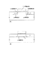
その他の方法として、図2(A)に示す様なDouble Implanted LDDと呼ばれる方法が挙げられる。これはイオン打ち込みによってn- 領域(LDD領域)201、202の直下またはそれを囲む様にやや弱めのP型(p- )領域203、204を設けた構造である。特にLDD領域を囲む様にして設けた場合にはポケット構造と呼ばれることもある。
【0011】
さらに、チャネル部の基板内部に基板より高濃度のp型領域(p- 領域)206を形成するパンチスルーストッパー構造(図2(B))も提案されている。これらの方法は、全て基板深さ方向、或いは、ゲイト(チャネル)長方向のエンジニアリングである。
【0012】
【発明が解決しようとする課題】
ところが、従来例の図2(A)、(B)に述べた様な構造ではいくつかの問題もある。図2(A)の構造は、ドレイン領域(LDD領域も含めて)の直下のみにp- 領域が設けられた構造であるため、あまり短チャネル効果の抑制効果を期待できない。
【0013】
また、ポケット構造と呼ばれるタイプではキャリア(電子を例にとる)はドレイン領域に到達する前に必ずp- 領域を通過することになるので、移動度の低下を招くといった問題が生じる。
【0014】
また、図2(B)の構造は通常ゲイト電極を形成した後に、スルードーピングによって深さ方向の濃度制御を行う。従って、濃度分布の制御が非常に困難である上、半導体層界面の結晶性を崩してしまうため、移動度を高めるためには好ましい手段とは言えない。
【0015】
そこで本願発明では、プロセス制御性の高い構造で効果的に短チャネル効果を抑制しうるMOSFETを提供することを課題とする。
【0016】
【課題を解決するための手段】
本願発明は、短チャネル効果を抑制するための不純物領域をチャネル幅方向に対して局所的(一か所乃至数カ所)に施すという構成を基本とする。即ち、チャネル幅方向にソース/ドレインとは逆導電型の高抵抗領域を形成することにより、ドレインからの空間電荷領域(空乏層)の広がりを抑制し、且つ、高オン電流を得ることが可能となる。
【0017】
従来の深さ、或いは、チャネル長方向のエンジニアリングに比べて、チャネル幅方向のエンジニアリングの優位性は、次の点にある。
(1)プロセス制御性が容易である。
(2)空間電荷領域抑制領域とチャネル形成領域とが分離しているので、反転層(チャネル領域)内における不純物濃度を低くすることが可能である(オン時の抵抗が小さくなりキャリア移動度が向上する)。
【0018】
なお、空間電荷領域抑制領域(空乏層抑制領域)とは、ドレイン側空乏層のソース側への広がりを抑えるために形成された不純物領域を指している。本発明者らは空乏層を抑止する効果があたかも空乏層をピン止めする様に捉えられることから、この領域をピニング領域(pinning region)と呼んでいる。
【0019】
【発明の実施の形態】
本願発明の実施の形態について、以下に示す実施例でもって詳細な説明を行うこととする。
【0020】
〔実施例1〕
本願発明のMOSFETの構成の一部(ソース/ドレイン電極は省略している)を図1に示す。図1(A)は上面図であり、図1(B)は図1(A)をA−A’で切った断面、図1(C)は図1(A)をB−B’で切った断面である。
【0021】
図1(A)、(B)、(C)において、101はソース領域、102はドレイン領域、103はフィールド酸化膜、104はゲイト電極である。そして、ゲイト電極104の下にもぐり込む様にして形成された不純物領域105が、本願発明の特徴であるピニング領域である。
【0022】
なお、本明細書中ではソース領域101、ドレイン領域102しか記載していないが、この中にはLDD領域やオフセット領域などの高抵抗領域も含めるものとする。重要なのはピニング領域をチャネル形成領域とドレイン領域との境界(接合部)付近に設けて空乏層の広がりを抑制するという構成であり、LDD構造やオフセット構造の有無は問題ではない。
【0023】
また、本明細書中においてチャネル形成領域とは、ゲイト電極の下に位置する半導体領域を指す。ピニング領域も半導体表面ではチャネルが形成されうるので広義な意味ではチャネル形成領域に含まれる。
【0024】
そこで本明細書ではチャネル形成領域をピニング領域(不純物領域)105と、不純物が添加されなかった領域(以下、アンドープ領域と呼ぶ)106とに区別して記載する。即ち、アンドープ領域とはシリコン基板濃度またはウェル濃度がそのまま残った領域と考えてよい。
【0025】
ところで、ピニング領域105はソース/ドレイン領域とは逆導電型の不純物を添加して形成される。空乏層はPN接合部の濃度差によって幅が決定するため、チャネル形成領域よりも濃度の高い領域を形成することで空乏層の広がりを抑えることができる。
【0026】
例えば、Nチャネル型MOSFETを形成するにあたってチャネル形成領域としてP型シリコン基板そのものを利用する場合、ピニング領域は基板よりも強いP型の不純物領域で構成すれば良い。
【0027】
具体的には、チャネル形成領域がP型ならば13族から選ばれた元素(代表的にはボロン)を添加して形成する。また、チャネル形成領域がN型ならば15族から選ばれた元素(代表的にはリン又は砒素)を添加すれば良い。勿論、チャネル形成領域はシリコン基板を利用するのであっても、不純物添加で形成したウェルを利用するのであっても良い。
【0028】
なお、上述の13族又は15族から選ばれた元素は単結晶シリコンのエネルギーバンドをシフトさせることでキャリア(電子または正孔)にとってのエネルギー障壁を形成している。そういった意味で、ピニング領域はエネルギーバンドをシフトさせてなる領域と呼ぶこともできる。
【0029】
不純物を添加しないアンドープ領域とピニング領域との間にはバンドギャップがシフトした分に相当するエネルギー差が生まれる。この電位的な障壁はしきい値電圧の相違といった形で現れる。
【0030】
この障壁の高さは実効キャリア濃度(N型、P型の相対的な濃度差)によって変化するが、不純物元素の添加濃度で調節できる。本願発明では、添加する不純物元素の濃度を1×10¹⁷〜5×10¹⁹atoms/cm3 (好ましくは1×10¹⁸〜5×10¹⁹atoms/cm3 )の範囲で調節する。
【0031】
また、ピニング領域105は、最も典型的には図1(A)に示す様にチャネル形成領域(ゲイト電極104直下の半導体領域)とソースまたはドレイン領域101、102との接合部に配列して形成される。即ち、接合部付近ではピニング領域105とアンドープ領域106とが交互に並んで配置される。
【0032】
この様子を断面で見ると、図1(B)に示す様になる。この様に、キャリアが優先的に移動する領域(アンドープ領域106)と空乏層を抑制する領域(ピニング領域105)とが分離されているため、キャリア移動度を低下させることなくTFTを動作させることが可能である。
【0033】
なお、図1(B)において100で示されるのは単結晶シリコン基板である。これはP型であってもN型であっても良い。本願発明では上述の特殊な構造によって短チャネル効果が抑制されるので、チャネル形成領域としてシリコン基板を用いる場合には、基板濃度を1×10¹⁶〜5×10¹⁷atoms/cm3 (好ましくは5×10¹⁶〜1×10¹⁷atoms/cm3 )と低めに抑えることができる。
【0034】
また、ピニング領域は少なくともドレイン側の接合部に設けられていれば短チャネル効果の抑制効果を得ることができる。ソース/ドレインが特定される様な回路に用いられるMOSFETの場合、ドレイン側のみにピニング領域を設ける様な構成として良い。
【0035】
ところで、前述の様なピニング領域105はゲイト電極104を形成した後、レジストマスクによって所定位置を隠した状態で不純物添加工程を行うことで形成することができる。この時、ゲイト電極104に対して斜め方向から不純物を添加することで、図1(C)に示す様にゲイト電極104の下にもぐり込む様な形状のピニング領域105を形成することが可能となる。チャネル形成領域とドレイン領域102との接合部付近に配列して形成されるピニング領域は、チャネル形成領域とソース領域101との接合部付近には達しない。つまりピニング領域は、チャネル形成領域とドレイン領域との接合部付近、及びチャネル形成領域とソース領域との接合部付近それぞれに配列して形成され、互いに分離して形成される。
【0036】
この斜めからの角度はシリコン基板の鉛直方向に対して7〜83°(好ましくは43±3°)で行うことが望ましい。0〜7°ではチャネリングを起こして不純物が深く打ち込まれ過ぎるので好ましくない。また、83〜90°では角度が浅すぎてゲイト電極の下に不純物を添加することが困難である。
【0037】
本実施例ではシリコン基板の面方位が(100)面であるため結晶学的には45°([110]方向を意味する)の時にチャネリングを起こして最も深くまで打ち込まれる。しかし本発明者らがシミュレーションによって計算した結果では、43°が最も好ましい角度であった。そのため、本願発明を実施するには43±3°とすることが望ましいと言える。
【0038】
また、その際、ピニング領域105の形成深さはソース/ドレイン領域の接合深さと同程度とすることが望ましい。従って、ピニング領域の形成深さは 0.02 〜0.3 μm(好ましくは 0.05 〜0.1 μm)となる様に調節する。
【0039】
なお、ピニング領域105の形成は非常に微細な加工技術を要する。レジストパターンを形成してイオンインプランテーション法等で不純物を打ち込む方法を用いる場合、非常に精密なフォトリソグラフィ技術が必要である。また、パターン形成時に電子描画を用いることも有効である。さらに、FIB(Focusd Ion Beam )法を用いてマスクレスで不純物を添加することも可能である。
【0040】
また、不純物を斜め方向から添加してピニング領域を形成すると、図3に示す様な形状でピニング領域が形成される。図3において、301はアンドープ領域、302はドレイン領域、303はゲイト絶縁膜、304はゲイト電極、305はピニング領域である。ピニング領域305の一部はチャネル形成領域とドレイン領域302との接合部に接している。
【0041】
斜めから不純物が打ち込まれることで、ピニング領域305はゲイト電極304の下にも形成される。この時、ピニング領域305を形成する際に不純物の散乱が起こるため、実際には設計上のピニング領域305aの周囲に散乱によって形成される弱い不純物領域305bを考慮する必要がある(実際にはもっと連続的に複雑な分布を示すがここでは簡略化して示す)。
【0042】
この弱い不純物領域305bは半導体表面(チャネルが形成される部分)にまで到達してしまうが、散乱によって回り込んだ不純物しか存在しないので実効キャリア濃度としては1×10¹⁷〜5×10¹⁷atoms/cm3 程度である。
【0043】
即ち、従来の0.2 μmルールのMOSFETではチャネル形成領域の実効キャリア濃度が1×10¹⁸atoms/cm3 程度が必要であることを鑑みれば、十分にチャネル形成領域として機能しうる領域であることが判る。また、従来のチャネルドープを施した構造よりも実効キャリア濃度の低い領域をキャリア(電子または正孔)が通過する分、高いオン電流を得ることができる。
【0044】
この傾向は弱い不純物領域305bの不純物濃度をイオン打ち込み条件によって低く抑えることでより顕著になる。この様に、本願発明ではゲイト電極直下の半導体表面は実質的に全てチャネル形成領域と見なして良い。
【0045】
さらに、図1(A)、(B)に示す様にピニング領域の間にはスリット状にアンドープな領域が存在するので、キャリアは優先的にそこを流れてドレイン領域に到達すると考えられる。
【0046】
即ち、従来例で述べたポケット構造はp- 領域がキャリアの移動を妨げていたのに対し、本願発明ではキャリアの通り道となる領域が残されているので、オン電流が低下するといった問題がない。
【0047】
以上の様に、本願発明のMOSFETはピニング領域によって短チャネル効果を抑制すると同時に、ピニング領域とは分離して形成されたアンドープ領域がソース−ドレイン間を結ぶので高い動作速度を維持することができる。
【0048】
ここでチャネル長およびチャネル幅の定義を図4を用いて行う。図4においてソース領域401とドレイン領域402との間の距離をチャネル長(L)と定義する。本願発明はこの長さが 0.3μm以下、典型的には0.05〜0.2 μmである微細なMOSFETに対して有効である。また、このチャネル長に沿った方向をチャネル長方向と呼ぶ。
【0049】
また、チャネル長方向と直交する方向におけるチャネル形成領域403の長さをチャネル幅(W)とする。なお、このチャネル幅に沿った方向をチャネル幅方向と呼ぶ。
【0050】
チャネル幅はどの様な回路として用いるかによって異なるが、チャネル長と同程度とする場合もあれば数百μmと広くする場合もある。例えば、モノリシック型LCDのバッファ回路やサンプリング回路の様に大電流を流す必要のある回路は数百μmのチャネル幅を必要とする。
【0051】
また、任意のピニング領域404の形成幅をピニング幅(vj )と定義する。ピニング幅に特に上限はないが、チャネル幅の1/3 以下でないとドレイン接合部のアンドープ領域が狭くなるので好ましくない。また、下限はフォトリソグラフィ技術のパターン加工精度の限界が下限となる。本願発明の場合、0.05〜0.3 μmの範囲が実質的なピニング幅と言えるであろう。ピニング領域404のチャネル長方向の長さは、チャネル長(L)よりも短い。
【0052】
さらに、隣接する個々のピニング領域間の間隔(wi )は少なくともソース/ドレインの接合深さの2倍以上として設計する必要がある。
【0053】
ピニング領域の深さはソース/ドレインの接合深さ程度であるので、不純物散乱によって接合深さと同程度だけ横方向へのパターン広がりが起こる。即ち、ピニング領域のパターン設計段階で接合深さの少なくとも2倍以上の間隔をあけておかないと、隣接するピニング領域が接触してしまい、アンドープ領域を塞いでしまい好ましくない。従って、本願発明ではwi は 0.04 〜0.6 μm(好ましくは 0.1〜0.2 μm) とすれば良い。
【0054】
勿論、ピニング領域間の間隔(wi )が広すぎてもピニング効果が弱まってしまうため、適切な間隔とすることが重要である。本発明者らはwi の上限をその基板濃度で形成しうる最大空乏層幅と考えている。
【0055】
即ち、アンドープ領域の実効キャリア濃度が1×10¹⁶atoms/cm3 程度ならば形成されるドレイン側の空乏層の幅は 0.3μm程度であるので、wi を 0.3μm以下とすることが好ましい。また、同様に実効キャリア濃度が1×10¹⁷atoms/cm3 程度ならばwi は 0.1μm以下とすれば良い。この様にアンドープ領域の実効キャリア濃度(基板濃度またはウェル濃度)が決まれば最大空乏層幅の決まるので、それを踏まえて設計を行えば良い。
【0056】
以上の様に、本願発明では短チャネル効果を抑制するためのエンジニアリングをチャネル幅方向に対して施している。基本的にはゲイト電極に対して斜め方向から不純物を添加するだけなのでプロセス的には簡易である。
【0057】
従来の技術と異なる点は、不純物を添加する際にチャネル幅方向に局在的に不純物領域(ピニング領域)を設けることで、MOSFETのモビリティを低下させることなく、短チャネル効果を抑制することができる点にある。
【0058】
ここで本願発明のMOSFETの効果を以下にまとめる。まず、第1の効果は短チャネル効果(特にパンチスルー現象)がドレイン接合部に設けられたピニング領域によって効果的に抑制される点である。そのため、スケーリング則に従って微細化を進めても空乏層の広がりによる悪影響を防ぐことができる。
【0059】
第2の効果は、MOSFETが動作している時のキャリア(電子または正孔)の移動は、アンドープ領域で優先的に行われるため非常に高速動作が可能な点である。アンドープ領域は基板濃度またはウェル濃度がそのまま残っている領域であるため、実効キャリア濃度は少なくとも5×10¹⁷atoms/cm3 以下(好ましくは1×10¹⁷atoms/cm3 以下)である。
【0060】
なお、例えばP型シリコン基板に対して1×10¹⁷atoms/cm3 の実効キャリア濃度を持つN型ウェルを形成する場合、P型シリコン基板のボロン濃度が 1×10¹⁶atoms/cm3 程度であれば、N型ウェルには1×10¹⁶atoms/cm3 程度のボロンと1〜2×10¹⁷atoms/cm3 程度のリンが含まれることになる。しかしながら、不純物散乱が問題となるのはその不純物濃度が 1×10¹⁷atoms/cm3 以上となった場合であるため、N型ウェル内のボロンは無視して良いと言える。
【0061】
また、従来のチャネルドープを用いた構造では1×10¹⁸atoms/cm3 程度の不純物がチャネル形成領域全面に添加されるので、不純物散乱の影響は非常に大きくなってしまう。その点、本願発明ではキャリアが優先的に通過する領域(アンドープ領域)の実効キャリア濃度は少なくとも5×10¹⁷atoms/cm3 以下(好ましくは1×10¹⁷atoms/cm3 以下)であるため、不純物散乱の影響はあっても極めて小さいという利点を持つ。
【0062】
第3の効果は、ソース領域側にピニング領域を設けた構成ではソース側のピニング領域が正孔の引き出し線として利用できる点にある。MOSFETの動作時、ドレイン接合部のインパクトイオン化現象によって発生した正孔は基板へと流れて寄生バイポーラを導通させる恐れがある。
【0063】
しかしながら、ソース側に設けられたピニング領域によってチャネル下部に移動してきた正孔をソース領域へと引き抜くことができるため、寄生バイポーラの導通によるソース−ドレイン間耐圧の低下を防ぐことができる。
【0064】
以上の様に、本願発明のMOSFETは短チャネル効果を抑制したまま素子サイズを微細化することができるため、高い信頼性を維持したまま、高い動作性能を実現することができる。さらに、キャリアの移動する領域に余計な不純物を打ち込む必要がないので、高いモビリティ(電界効果移動度)を有するMOSFETを実現しうる。
【0065】
なお、本実施例ではNチャネル型MOSFETを例にとって説明を行ったが、同様にしてPチャネル型MOSFETに適用することもできる。その場合、ピニング領域に打ち込む不純物の導電型を変更すれば良いだけである。
【0066】
〔実施例2〕
本実施例では、実施例1に示した構造を有する本願発明のMOSFETを利用してCMOS回路を構成した場合の例について図5を用いて説明する。
【0067】
まず、P型単結晶シリコン基板501を準備し、不純物イオン注入によってP型ウェル502、N型ウェル503を形成する。この様な構成はいわゆるツインタブ構造であり、ウェル濃度は実施例1に示した様に 1×10¹⁶〜 5×10¹⁷atoms/cm3 の範囲で形成される。
【0068】
次に、公知のLOCOS法などにより選択酸化を行い、フィールド酸化膜504を形成した後、熱酸化工程によってシリコン表面に30nm厚の酸化膜(後のゲイト絶縁膜)505を形成する。(図5(A))
【0069】
次に、ゲイト電極506、507を形成する。本実施例ではゲイト電極を構成する材料として導電性を有するシリコン膜を用いるが、他にもタンタル、クロム、タングステン、モリブデン等の導電膜を用いることができる。なお、本実施例ではゲイト電極幅を 0.18 μmとする。
【0070】
ゲイト電極を形成したら、後にPチャネル型MOSFETとなる領域(図面向かって右側)をレジストマスク508で覆い、その状態で斜め方向から13族から選ばれた元素(代表的にはボロン)を添加する。
【0071】
また、Nチャネル型MOSFETとなる領域(図面向かって左側)に対しても、ピニング領域を形成するためのマスクをレジストマスク508と同時に形成する。この様子を図8に示す。図8において、800はシリコン基板、801はゲイト電極である。
【0072】
この時、ゲイト電極801を横切る様にしてストライプ状にレジストマスク802を形成する。即ち、マスク802で隠された部分がアンドープ領域となり、露出した部分(ただしゲイト電極801の下の部分)がピニング領域となる。
【0073】
なお、ここで形成される不純物領域は非常に狭い範囲に打ち込まれることになるのでできるだけ不純物散乱の影響を受けない様な装置や条件を用いて添加することが望ましい。
【0074】
そこで本実施例では、イオンインプランテーション法(イオン注入法)によりボロンを 1×10¹⁸atoms/cm3 の濃度で添加する。また、注入ガスはBF2 、加速電圧は30keV 、ドーズ量は 1×10¹³atoms/cm2 とする。そして、シリコン基板に対して30°の角度でイオンが注入される様に調節する。
【0075】
この様な条件はシミュレーションによって予め決定することができる。本発明者らによるシミュレーション結果では、本実施例の条件に従えば図10に示した様なプロファイルで不純物が添加されることが確認されている。
【0076】
こうして後にピニング領域となる不純物領域509、510が形成される。実際にはこれらの領域509、510の先端部分(ゲイト電極の下にもぐり込んだ部分)のみがピニング領域として機能する。(図5(B))
【0077】
次に、今度はシリコン基板に対して垂直に15族から選ばれた不純物元素を添加する。本実施例では不純物として砒素を用い、 5×10¹⁸〜 1×10¹⁹atoms/cm3 となる様に添加条件を調節する。ここでは20〜40nm程度の浅い接合を形成するためにイオンプランテーション法、プラズマドーピング法、レーザードーピング法のいずれかの手段を用いる。
【0078】
こうして形成される不純物領域511、512の一部は後にNチャネル型MOSFETのLDD(Lightly doped drain )領域として機能する。(図5(C))
【0079】
次に、Nチャネル型MOSFETとなる領域をレジストマスク513で覆う。この時、Pチャネル型MOSFETとなる領域には図8に示した様な構造でピニング領域形成用のマスクが設けられている(図示せず)。
【0080】
こうしてレジストマスク513を形成したら、シリコン基板に対して斜め方向から15族から選ばれた元素(代表的にはリン)を添加して後にピニング領域となる不純物領域514、515を形成する。添加条件はシミュレーションで前もって実験的に決定しておく。
【0081】
本実施例では、イオンインプランテーション法(イオン注入法)によりリン 1×10¹⁸atoms/cm3 の濃度で添加する。また、注入ガスはPH3 、加速電圧は30keV 、ドーズ量は 1×10¹³atoms/cm2 とする。そして、シリコン基板に対して30°の角度でイオンが注入される様に調節する。(図6(A))
【0082】
さらに、シリコン基板に対して垂直にボロンを添加し、後にPチャネル型MOSFETのLDD領域として機能する不純物領域516、517を形成する。この場合も浅い接合を形成することが望ましい。(図6(B))
【0083】
図6(B)の状態が得られたら、次に酸化珪素膜(図示せず)を堆積してエッチバックを行い、サイドウォール518、519を形成する。(図6(C))
【0084】
次に、再びPチャネル型MOSFETとなる領域をレジストマスク520で覆い、砒素を 1×10²⁰atoms/cm3 の濃度で添加する。こうしてソース領域521、ドレイン領域522が形成され、サイドウォール518の下にはLDD領域523が形成される。(図7(A))
【0085】
なお、ソース/ドレイン領域を形成する場合もイオンプランテーション法、プラズマドーピング法、レーザードーピング法のいずれかの手段を用いて浅い接合を形成することが望ましい。
【0086】
また、同様にNチャネル型MOSFETとなる領域をレジストマスク524で覆い、ボロンを 1×10²⁰atoms/cm3 の濃度で添加する。こうしてドレイン領域525、ソース領域526が形成され、サイドウォール519の下にはLDD領域527が形成される。(図7(B))
【0087】
図7(B)の状態が得られたら、熱またはレーザーによるアニール処理を行い、添加した不純物の活性化を行う。この時、不純物の拡散をできるだけ小さくする様な条件を設定することが必要である。
【0088】
ソース/ドレイン領域の活性化が終了したら、チタン膜を成膜してアニール処理を行い、ソース/ドレイン領域及びゲイト電極の表面にチタンシリサイド層528を形成する。勿論、他の金属膜を用いた金属シリサイドを形成することもできる。シリサイド層を形成した後、チタン膜は除去する。
【0089】
次に、層間絶縁膜529を形成し、コンタクトホールを開けてソース電極530、531、ドレイン電極532を形成する。勿論、電極形成後に水素化を行うことも有効である。
【0090】
以上の様な工程によって、図7(C)に示す様なCMOS回路を得ることができる。このCMOS回路はNチャネル型、Pチャネル型の両MOSFETに対してピニング領域を設けているが、どちらか一方のみに設けた構成とすることも可能である。
【0091】
〔実施例3〕
実施例1、2ではゲイト電極の両側から斜めに不純物を添加することでソース接合部とドレイン接合部とにピニング領域を形成している。この時、ソース/ドレイン接合部の両方に設けられたピニング領域が、互いにゲイト電極の直下で電気的に接続する様な構成としても良い。
【0092】
本実施例の構造を図9に示す。図9は本願発明の構造を有するNチャネル若しくはPチャネル型のMOSFETである。注目すべきは、斜め添加によって形成されたピニング領域がゲイト電極直下で接触し、ソース−ドレイン間に渡る一つのピニング領域901を形成している点である。
【0093】
勿論、ピニング領域901は図1で説明した様にチャネル幅方向に対してスリット状に設けられた構成となっており、チャネル幅方向に対して配列された各ピニング領域間にはアンドープ領域(図示せず)が形成されている。
【0094】
本実施例の構造とすると、実効的なアンドープ領域の面積は減少するがドレイン側からの空乏層の広がりを抑えるピニング効果が高まる。なお、チャネル長が 0.1μm以下となってしまうと不純物添加の制御性の問題から必然的に本実施例の構造になると予想される。
【0095】
〔実施例4〕
本願発明は、埋め込みチャネル型のMOSFETに対して適用することも可能である。埋め込みチャネル型はゲイト絶縁膜との界面よりも下にチャネルが形成され、そこをキャリアが移動する。
【0096】
従って、表面散乱によるキャリア移動度の低下がなく、表面チャネル型に比べて高いモビリティを得ることができる。しかし一方で埋め込みチャネル型はパンチスルーに弱く、耐圧特性が低いという欠点がある。
【0097】
しかしながら、本願発明の構造を採用した埋め込みチャネル型MOSFETは高いモビリティを維持したままパンチスルーによるソース−ドレイン間耐圧の低下を抑止することが可能である。
【0098】
〔実施例5〕
本願発明は従来のIC技術全般に適用することが可能である。即ち、現在市場に流通している全ての半導体装置(MOSFETを部品として含む製品)に適用しうる。なお、本明細書中において「半導体装置」とは、単体素子だけでなく、複数の単体素子で構成された集積化回路およびその様な集積化回路を搭載した電子機器(応用製品)をも範疇に含むものとする。
【0099】
例えば、ワンチップ上に集積化されたRISCプロセッサ、ASICプロセッサ等のマイクロプロセッサに適用しうる。また、D/Aコンバータ等の信号処理回路から携帯機器(携帯電話、PHS、モバイルコンピュータ)用の高周波回路に至るまで、半導体を利用する全ての集積化回路に適用しうる。
【0100】
図11に示すのは、マイクロプロセッサの一例である。マイクロプロセッサは典型的にはCPUコア11、RAM12、クロックコントローラ13、キャッシュメモリー14、キャッシュコントローラ15、シリアルインターフェース16、I/Oポート17等から構成される。
【0101】
勿論、図11に示すマイクロプロセッサは簡略化した一例であり、実際のマイクロプロセッサはその用途によって多種多様な回路設計が行われる。
【0102】
しかし、どの様な機能を有するマイクロプロセッサであっても中枢として機能するのはIC(Integrated Circuit)18である。IC18は半導体チップ19上に形成された集積化回路をセラミック等で保護した機能回路である。
【0103】
そして、その半導体チップ19上に形成された集積化回路を構成するのが本願発明の構造を有するMOSFET20(Nチャネル型)、20(Pチャネル型)である。なお、基本的な回路はCMOS回路を最小単位として構成することで消費電力を抑えることができる。
【0104】
また、本実施例に示したマイクロプロセッサは様々な電子機器に搭載されて中枢回路として機能する。代表的な電子機器としてはパーソナルコンピュータ、携帯型情報端末機器、その他あらゆる家電製品が挙げられる。また、車両(自動車や電車等)の制御用コンピュータなども挙げられる。
【0105】
【発明の効果】
本願発明によりディープサブミクロンプロセスが必要となってもプロセス制御性の高い構造で効果的に短チャネル効果を抑制しうるMOSFETを提供することが可能となる。
【0106】
さらに、キャリアの移動経路となる領域が確保されているので短チャネル効果の抑制と同時に高いモビリティを有するMOSFETが実現される。即ち、高いモビリティと高い信頼性とを同時に実現する半導体装置が得られる。
【0107】
本願発明を利用した半導体装置は、今現在市場に流通している全ての半導体装置(応用製品も含めて)と置き換えが可能であり、全ての半導体装置の高性能化、高信頼性化を実現しうる。
【図面の簡単な説明】
【図1】 本願発明のMOSFET構造を説明するための図。
【図2】 従来のMOSFET構造を説明するための図。
【図3】 ピニング領域の形状を示す図。
【図4】 ピニング領域の配置構成を示す図。
【図5】 本願発明のMOSFETの作製工程を示す図。
【図6】 本願発明のMOSFETの作製工程を示す図。
【図7】 本願発明のMOSFETの作製工程を示す図。
【図8】 ピニング領域形成時のレジストの配置例を示す図。
【図9】 本願発明のMOSFET構造を説明するための図。
【図10】 ピニング領域形成時のシミュレーション結果を示す図。
【図11】 電子機器の一例を示す図。[0001]
[Technical field to which the invention belongs]
The present invention relates to a structure of a semiconductor device formed using a single crystal silicon substrate, particularly an insulated gate field effect transistor (referred to as MOSFET or IGFET). In particular, this technique is effective when a microelement having a channel length of 0.3 μm or less (typically 0.05 to 0.2 μm) is manufactured.
[0002]
Further, the present invention can be applied to various semiconductor circuits such as ICs, VLSIs, ULSIs and the like that are configured by integrating MOSFETs.
[0003]
[Prior art]
The MOSFET changes the potential of the semiconductor (silicon) interface immediately below the gate by the gate voltage, and controls on / off of the electron flow or the hole flow between the source and the drain.
[0004]
However, when the channel length of the transistor is shortened, the space charge region (also referred to as a depletion layer) in the vicinity of the source and the drain comes into contact. At this time, the potential at the semiconductor interface close to the gate can be controlled by the gate potential, but the potential at the deep part from the gate remains high under the influence of the drain voltage even if the gate voltage is lowered.
[0005]
That is, even if the gate voltage is set to 0 V in order to turn off the transistor, a leakage current flows through the high potential portion (the portion where the space charge region is widened) of the semiconductor substrate. This is called the short channel effect and appears as a phenomenon such as an increase in S value (subthreshold coefficient) or a decrease in threshold voltage.
[0006]
As a phenomenon in which the short channel effect is large, punch-through in which current continues to flow occurs. The merit to miniaturization of the MOSFET is to lower the voltage and increase the speed. For this success, suppression of the short channel effect and reduction of the resistance at the time of ON are the keys.
[0007]
A scaling method proposed by Dennard in 1974 is a measure for miniaturizing MOSFETs while suppressing the short channel effect. In order to shorten the gate length while suppressing the short channel effect from this method, (1) make the gate insulating film thin, (2) make the source / drain junction depth shallow, and (3) the space charge region. A means of suppressing the width (depletion layer width) is effective.
[0008]
For (1), the current limit of 3 nm is the limit. With regard to (2), devices such as an ion doping apparatus and laser doping have been studied, but various problems remain for deep submicron sizes and below.
[0009]
As a method of (3), the first possible method is to increase the concentration of the channel formation region, that is, channel doping. However, in order to form a MOSFET with fine dimensions such as 0.18 μm rule, 1 × 10¹⁸atoms / cmThree It is necessary to add a certain amount of impurities, which causes a significant decrease in on-current.
[0010]
As another method, there is a method called Double Implanted LDD as shown in FIG. This is due to ion implantation-P type (p) slightly weaker so as to be directly under or surrounding the regions (LDD regions) 201 and 202-) A structure provided with regions 203 and 204. In particular, when it is provided so as to surround the LDD region, it may be called a pocket structure.
[0011]
Furthermore, a p-type region (p-A punch-through stopper structure (FIG. 2B) for forming (region) 206 has also been proposed. These methods are all engineering in the substrate depth direction or in the gate (channel) length direction.
[0012]
[Problems to be solved by the invention]
However, the structure as shown in FIGS. 2A and 2B of the conventional example has some problems. The structure of FIG. 2 (A) has a p-type structure just below the drain region (including the LDD region).-Since the structure is provided with a region, the effect of suppressing the short channel effect cannot be expected.
[0013]
Also, in the type called pocket structure, carriers (for example, electrons) must be p before reaching the drain region.-Since it passes through the region, there arises a problem that the mobility is lowered.
[0014]
In addition, FIG.BIn the structure of (1), after the gate electrode is formed, the concentration in the depth direction is controlled by through doping. Therefore, it is very difficult to control the concentration distribution, and the crystallinity at the interface of the semiconductor layer is destroyed. Therefore, it cannot be said that it is a preferable means for increasing the mobility.
[0015]
Therefore, an object of the present invention is to provide a MOSFET capable of effectively suppressing the short channel effect with a structure having high process controllability.
[0016]
[Means for Solving the Problems]
The present invention basically has a configuration in which an impurity region for suppressing the short channel effect is locally (one to several places) in the channel width direction. In other words, by forming a high resistance region opposite to the source / drain in the channel width direction, the spread of the space charge region (depletion layer) from the drain can be suppressed and a high on-current can be obtained. It becomes.
[0017]
The superiority of engineering in the channel width direction compared to conventional engineering in the depth or channel length direction is as follows.
(1) Process controllability is easy.
(2) Since the space charge region suppression region and the channel formation region are separated, it is possible to reduce the impurity concentration in the inversion layer (channel region) (the resistance at the time of ON is reduced and the carrier mobility is reduced). improves).
[0018]
The space charge region suppression region (depletion layer suppression region) refers to an impurity region formed in order to suppress the drain side depletion layer from spreading to the source side. The present inventors refer to this region as a pinning region because the effect of suppressing the depletion layer can be understood as if the depletion layer is pinned.
[0019]
DETAILED DESCRIPTION OF THE INVENTION
The embodiment of the present invention will be described in detail with the following examples.
[0020]
[Example 1]
A part of the structure of the MOSFET of the present invention (source / drain electrodes are omitted) is shown in FIG. 1A is a top view, FIG. 1B is a cross-sectional view taken along line AA ′ of FIG. 1A, and FIG. 1C is a cross-sectional view taken along line BB ′ of FIG. It is a cross section.
[0021]
In FIGS. 1A, 1B, and 1C, 101 is a source region, 102 is a drain region, 103 is a field oxide film, and 104 is a gate electrode. The
[0022]
Note that although only the
[0023]
In this specification, a channel formation region refers to a semiconductor region located under a gate electrode. The pinning region is also included in the channel formation region in a broad sense because a channel can be formed on the semiconductor surface.
[0024]
Therefore, in this specification, a channel formation region is described separately as a pinning region (impurity region) 105 and a region (hereinafter referred to as an undoped region) 106 to which no impurity is added. That is, the undoped region may be considered as a region where the silicon substrate concentration or well concentration remains as it is.
[0025]
Incidentally, the pinning
[0026]
For example, when a P-type silicon substrate itself is used as a channel formation region when forming an N-channel MOSFET, the pinning region may be formed of a P-type impurity region stronger than the substrate.
[0027]
Specifically, if the channel formation region is P-type, it is formed by adding an element selected from group 13 (typically boron). If the channel formation region is N-type, an element selected from Group 15 (typically phosphorus or arsenic) may be added. Of course, the channel formation region may use a silicon substrate or a well formed by adding impurities.
[0028]
Note that an element selected from
[0029]
An energy difference corresponding to the shift of the band gap is generated between the undoped region to which no impurity is added and the pinning region. This potential barrier appears in the form of a difference in threshold voltage.
[0030]
The height of the barrier varies depending on the effective carrier concentration (the relative concentration difference between the N-type and P-type), but can be adjusted by adding the impurity element. In the present invention, the concentration of the impurity element to be added is 1 × 10¹⁷~ 5 × 10¹⁹atoms / cmThree (Preferably 1 × 10¹⁸~ 5 × 10¹⁹atoms / cmThree ) Adjust within the range.
[0031]
Further, the pinning
[0032]
When this state is viewed in a cross section, it is as shown in FIG. In this manner, since the region where carriers move preferentially (undoped region 106) and the region where the depletion layer is suppressed (pinning region 105) are separated, the TFT can be operated without lowering the carrier mobility. Is possible.
[0033]
Note that a single crystal silicon substrate is denoted by 100 in FIG. This may be P-type or N-type. In the present invention, the short channel effect is suppressed by the above-described special structure. Therefore, when a silicon substrate is used as the channel formation region, the substrate concentration is set to 1 × 10 6.16~ 5 × 10¹⁷atoms / cmThree (Preferably 5 × 10¹⁶~ 1 × 10¹⁷atoms / cmThree ) And lower.
[0034]
Moreover, if the pinning region is provided at least at the junction on the drain side, the effect of suppressing the short channel effect can be obtained. In the case of a MOSFET used in a circuit in which a source / drain is specified, a configuration in which a pinning region is provided only on the drain side may be used.
[0035]
By the way, the pinning
[0036]
It is desirable that the oblique angle is 7 to 83 ° (preferably 43 ± 3 °) with respect to the vertical direction of the silicon substrate. If it is 0-7 °, channeling occurs and impurities are implanted too deeply, which is not preferable. Further, when the angle is 83 to 90 °, the angle is too shallow and it is difficult to add impurities under the gate electrode.
[0037]
In this embodiment, since the plane orientation of the silicon substrate is the (100) plane, crystallographically, channeling occurs at 45 ° (meaning the [110] direction), and the silicon substrate is implanted to the deepest. However, according to the results calculated by the inventors through simulation, 43 ° was the most preferable angle. Therefore, it can be said that it is desirable to set it as 43 +/- 3 degrees in order to implement this invention.
[0038]
At this time, it is desirable that the formation depth of the pinning
[0039]
Note that the formation of the pinning
[0040]
Further, when a pinning region is formed by adding impurities from an oblique direction, the pinning region is formed in a shape as shown in FIG. In FIG. 3, 301 is an undoped region, 302 is a drain region, 303 is a gate insulating film, 304 is a gate electrode, and 305 is a pinning region.A part of the pinning region 305 is in contact with the junction between the channel formation region and the drain region 302.
[0041]
The pinning region 305 is also formed under the gate electrode 304 by implanting impurities from an oblique direction. At this time, since impurity scattering occurs when the pinning region 305 is formed, it is actually necessary to consider the weak impurity region 305b formed by scattering around the designed pinning region 305a (in practice, more It shows a continuously complex distribution, but here it is simplified.)
[0042]
This weak impurity region 305b reaches the semiconductor surface (portion forming portion), but since only impurities that have wrap around due to scattering exist, the effective carrier concentration is 1 × 10 6.17~ 5 × 10¹⁷atoms / cmThree Degree.
[0043]
That is, in the conventional 0.2 μm rule MOSFET, the effective carrier concentration in the channel formation region is 1 × 10 6.18atoms / cmThree In view of the necessity of the degree, it can be seen that the region can sufficiently function as a channel formation region. In addition, a higher on-current can be obtained because carriers (electrons or holes) pass through a region having a lower effective carrier concentration than a conventional channel-doped structure.
[0044]
This tendency becomes more prominent by suppressing the impurity concentration of the weak impurity region 305b to be low depending on the ion implantation conditions. As described above, in the present invention, the semiconductor surface directly under the gate electrode may be substantially regarded as a channel formation region.
[0045]
Further, as shown in FIGS. 1A and 1B, since there is an undoped region in the form of slits between the pinning regions, it is considered that carriers preferentially flow there and reach the drain region.
[0046]
That is, the pocket structure described in the conventional example is p.-Whereas the region hinders the movement of the carrier, the present invention does not have a problem that the on-current decreases because the region that becomes the path of the carrier remains.
[0047]
As described above, the MOSFET of the present invention suppresses the short channel effect by the pinning region, and at the same time can maintain a high operation speed because the undoped region formed separately from the pinning region connects the source and drain. .
[0048]
Here, the channel length and channel width are defined with reference to FIG. In FIG. 4, the distance between the source region 401 and the drain region 402 is defined as a channel length (L). The present invention is effective for a fine MOSFET having a length of 0.3 μm or less, typically 0.05 to 0.2 μm. A direction along the channel length is referred to as a channel length direction.
[0049]
Further, the length of the channel formation region 403 in a direction orthogonal to the channel length direction is defined as a channel width (W). The direction along the channel width is referred to as the channel width direction.
[0050]
The channel width varies depending on the circuit used, but it may be as large as the channel length or may be as wide as several hundred μm. For example, a circuit that requires a large current to flow, such as a buffer circuit or a sampling circuit of a monolithic LCD, requires a channel width of several hundreds of μm.
[0051]
Further, the formation width of an arbitrary pinning region 404 is set to the pinning width (vj). Although there is no particular upper limit to the pinning width, it is not preferable that the undoped region of the drain junction is narrowed unless the channel width is 1/3 or less. Further, the lower limit is the limit of the pattern processing accuracy of the photolithography technique. In the case of the present invention, a range of 0.05 to 0.3 μm can be said to be a substantial pinning width.The length of the pinning region 404 in the channel length direction is shorter than the channel length (L).
[0052]
Furthermore, the spacing between adjacent individual pinning regions (wi) Must be designed to be at least twice the source / drain junction depth.
[0053]
Since the depth of the pinning region is about the junction depth of the source / drain, the pattern spread in the lateral direction is caused by the impurity scattering to the same extent as the junction depth. That is, it is not preferable that an adjacent pinning region is brought into contact with an undoped region unless an interval of at least twice the junction depth is provided at the pattern design stage of the pinning region. Therefore, in the present invention, wiMay be 0.04 to 0.6 μm (preferably 0.1 to 0.2 μm).
[0054]
Of course, the interval between the pinning regions (wi) Is too wide, the pinning effect is weakened, so it is important to set an appropriate interval. We have wiIs considered to be the maximum depletion layer width that can be formed at the substrate concentration.
[0055]
That is, the effective carrier concentration in the undoped region is 1 × 10¹⁶atoms / cmThree If so, the width of the depletion layer on the drain side is about 0.3 μm.iIs preferably 0.3 μm or less. Similarly, the effective carrier concentration is 1 × 10.17atoms / cmThree If it is about wiShould be 0.1 μm or less. In this way, if the effective carrier concentration (substrate concentration or well concentration) of the undoped region is determined, the maximum depletion layer width is determined.
[0056]
As described above, in the present invention, engineering for suppressing the short channel effect is performed in the channel width direction. Basically, the process is simple because impurities are simply added to the gate electrode from an oblique direction.
[0057]
The difference from the conventional technique is that when the impurity is added, an impurity region (pinning region) is locally provided in the channel width direction, thereby suppressing the short channel effect without reducing the mobility of the MOSFET. It is in a point that can be done.
[0058]
Here, the effects of the MOSFET of the present invention are summarized as follows. First, the first effect is that the short channel effect (particularly the punch-through phenomenon) is effectively suppressed by the pinning region provided at the drain junction. Therefore, adverse effects due to the spread of the depletion layer can be prevented even if miniaturization is advanced according to the scaling law.
[0059]
The second effect is that the movement of carriers (electrons or holes) when the MOSFET is operating is preferentially performed in the undoped region, so that a very high speed operation is possible. Since the undoped region is a region where the substrate concentration or well concentration remains as it is, the effective carrier concentration is at least 5 × 10 5.17atoms / cmThree Below (preferably 1 x 10¹⁷atoms / cmThree The following).
[0060]
For example, 1 × 10 for P-type silicon substrate17atoms / cmThree When forming an N-type well with an effective carrier concentration, the boron concentration of the P-type silicon substrate is 1 × 10¹⁶atoms / cmThree 1 x 10 for N-type wells16atoms / cmThree About boron and 1-2 × 10¹⁷atoms / cmThree About phosphorus will be included. However, the problem of impurity scattering is that the impurity concentration is 1 × 10¹⁷atoms / cmThree Since this is the case, it can be said that boron in the N-type well can be ignored.
[0061]
Also, the conventional structure using channel dope is 1 × 10¹⁸atoms / cmThree Since a certain amount of impurities are added to the entire surface of the channel formation region, the influence of impurity scattering becomes very large. In that respect, in the present invention, the effective carrier concentration in the region through which carriers pass preferentially (undoped region) is at least 5 × 10 5.17atoms / cmThree Below (preferably 1 x 10¹⁷atoms / cmThree Therefore, there is an advantage that even if there is an influence of impurity scattering, it is extremely small.
[0062]
The third effect is that in the configuration in which the pinning region is provided on the source region side, the source side pinning region can be used as a hole lead-out line. During the operation of the MOSFET, holes generated by the impact ionization phenomenon at the drain junction may flow to the substrate and make the parasitic bipolar conductive.
[0063]
However, since the holes that have moved to the lower part of the channel can be extracted to the source region by the pinning region provided on the source side, it is possible to prevent a decrease in the source-drain breakdown voltage due to the conduction of the parasitic bipolar.
[0064]
As described above, since the MOSFET of the present invention can reduce the element size while suppressing the short channel effect, high operating performance can be realized while maintaining high reliability. Furthermore, since it is not necessary to implant extra impurities in the region where carriers move, a MOSFET having high mobility (field effect mobility) can be realized.
[0065]
In this embodiment, an N-channel MOSFET has been described as an example. However, the present invention can be similarly applied to a P-channel MOSFET. In that case, it is only necessary to change the conductivity type of the impurity implanted into the pinning region.
[0066]
[Example 2]
In this embodiment, an example in which a CMOS circuit is configured using the MOSFET of the present invention having the structure shown in Embodiment 1 will be described with reference to FIG.
[0067]
First, a P-type single
[0068]
Next, after selective oxidation is performed by a known LOCOS method or the like to form a
[0069]
Next,
[0070]
After forming the gate electrode, a region (right side in the drawing) that will be a P-channel MOSFET is covered with a resist
[0071]
In addition, a mask for forming a pinning region is formed at the same time as the resist
[0072]
At this time, a resist mask 802 is formed in a stripe shape so as to cross the gate electrode 801. That is, a portion hidden by the mask 802 becomes an undoped region, and an exposed portion (however, a portion under the gate electrode 801) becomes a pinning region.
[0073]
Since the impurity region formed here is implanted in a very narrow range, it is desirable to add it using an apparatus and conditions that are not affected by impurity scattering as much as possible.
[0074]
Therefore, in this example, boron is ionized by 1 × 10 by the ion implantation method (ion implantation method).18atoms / cmThree Add at a concentration of The injection gas is BF2 , Acceleration voltage is 30keV, dose is 1 × 10¹³atoms / cm2 And Then, adjustment is performed so that ions are implanted at an angle of 30 ° with respect to the silicon substrate.
[0075]
Such conditions can be determined in advance by simulation. According to the simulation results by the present inventors, it has been confirmed that impurities are added with a profile as shown in FIG. 10 according to the conditions of this embodiment.
[0076]
In this way,
[0077]
Next, an impurity element selected from Group 15 is added perpendicularly to the silicon substrate. In this example, arsenic is used as an impurity and 5 × 10¹⁸~ 1 × 10¹⁹atoms / cmThree Adjust the addition conditions so that Here, any of an ion plantation method, a plasma doping method, and a laser doping method is used to form a shallow junction of about 20 to 40 nm.
[0078]
Part of the
[0079]
Next, a region to be an N-channel MOSFET is covered with a resist
[0080]
After the resist
[0081]
In the present example, phosphorus 1 × 10 5 by ion implantation (ion implantation) is used.18atoms / cmThree Add at a concentration of The injection gas is PHThree , Acceleration voltage is 30keV, dose is 1 × 10¹³atoms / cm2 And Then, adjustment is performed so that ions are implanted at an angle of 30 ° with respect to the silicon substrate. (Fig. 6 (A))
[0082]
Further, boron is added perpendicularly to the silicon substrate, and
[0083]
After the state shown in FIG. 6B is obtained, a silicon oxide film (not shown) is deposited and etched back to
[0084]
Next, the region that becomes the P-channel type MOSFET is again covered with a resist
[0085]
Even when the source / drain regions are formed, it is desirable to form a shallow junction using any one of an ion plantation method, a plasma doping method, and a laser doping method.
[0086]
Similarly, a region to be an N-channel MOSFET is covered with a resist
[0087]
When the state shown in FIG. 7B is obtained, annealing with heat or laser is performed to activate the added impurities. At this time, it is necessary to set conditions for minimizing impurity diffusion.
[0088]
When the activation of the source / drain regions is completed, a titanium film is formed and annealed to form a
[0089]
Next, an
[0090]
Through the above steps, a CMOS circuit as shown in FIG. 7C can be obtained. In this CMOS circuit, a pinning region is provided for both N-channel and P-channel MOSFETs, but a configuration in which only one of them is provided is also possible.
[0091]
Example 3
In the first and second embodiments, the pinning regions are formed at the source junction and the drain junction by adding impurities obliquely from both sides of the gate electrode. At this time, the pinning regions provided at both the source / drain junctions may be electrically connected to each other directly below the gate electrode.
[0092]
The structure of this example is shown in FIG. FIG. 9 shows an N-channel or P-channel MOSFET having the structure of the present invention. It should be noted that the pinning region formed by the oblique addition is in contact immediately under the gate electrode to form one pinning region 901 extending between the source and the drain.
[0093]
Of course, the pinning region 901 has a configuration provided in a slit shape in the channel width direction as described in FIG. 1, and an undoped region (see FIG. 5) is provided between the pinning regions arranged in the channel width direction. (Not shown) is formed.
[0094]
With the structure of this embodiment, the area of the effective undoped region is reduced, but the pinning effect for suppressing the spread of the depletion layer from the drain side is enhanced. If the channel length is 0.1 μm or less, the structure of this embodiment is inevitably expected due to the problem of controllability of impurity addition.
[0095]
Example 4
The present invention can also be applied to a buried channel type MOSFET. In the buried channel type, a channel is formed below the interface with the gate insulating film, and carriers move there.
[0096]
Accordingly, there is no decrease in carrier mobility due to surface scattering, and high mobility can be obtained as compared with the surface channel type. However, on the other hand, the buried channel type has a drawback that it is weak against punch-through and has a low withstand voltage characteristic.
[0097]
However, the buried channel MOSFET adopting the structure of the present invention can suppress a decrease in the breakdown voltage between the source and the drain due to punch-through while maintaining high mobility.
[0098]
Example 5
The present invention can be applied to all conventional IC technologies. That is, the present invention can be applied to all semiconductor devices (products including MOSFETs as parts) currently on the market. In the present specification, the term “semiconductor device” includes not only a single element but also an integrated circuit composed of a plurality of single elements and an electronic device (applied product) equipped with such an integrated circuit. To include.
[0099]
For example, the present invention can be applied to a microprocessor such as a RISC processor or an ASIC processor integrated on one chip. Further, the present invention can be applied to all integrated circuits using semiconductors from signal processing circuits such as D / A converters to high-frequency circuits for portable devices (mobile phones, PHS, mobile computers).
[0100]
FIG. 11 shows an example of a microprocessor. The microprocessor typically includes a CPU core 11, a RAM 12, a
[0101]
Needless to say, the microprocessor illustrated in FIG. 11 is a simplified example, and various circuit designs are performed on an actual microprocessor depending on the application.
[0102]
However, it is an IC (Integrated Circuit) 18 that functions as the center of a microprocessor having any function. The IC 18 is a functional circuit in which an integrated circuit formed on the semiconductor chip 19 is protected with ceramic or the like.
[0103]
The MOSFETs 20 (N channel type) and 20 (P channel type) having the structure of the present invention constitute the integrated circuit formed on the semiconductor chip 19. Note that power consumption can be suppressed by configuring a basic circuit with a CMOS circuit as a minimum unit.
[0104]
The microprocessor shown in this embodiment is mounted on various electronic devices and functions as a central circuit. Typical electronic devices include personal computers, portable information terminal devices, and all other home appliances. Further, a computer for controlling a vehicle (such as an automobile or a train) may be used.
[0105]
【The invention's effect】
According to the present invention, it is possible to provide a MOSFET capable of effectively suppressing the short channel effect with a structure having high process controllability even when a deep submicron process is required.
[0106]
Furthermore, since a region serving as a carrier movement path is secured, a MOSFET having high mobility at the same time as suppression of the short channel effect is realized. That is, a semiconductor device that achieves high mobility and high reliability at the same time can be obtained.
[0107]
The semiconductor device using the present invention can be replaced with all semiconductor devices (including applied products) currently on the market, realizing high performance and high reliability of all semiconductor devices. Yes.
[Brief description of the drawings]
FIG. 1 is a view for explaining a MOSFET structure of the present invention.
FIG. 2 is a diagram for explaining a conventional MOSFET structure;
FIG. 3 is a diagram showing the shape of a pinning region.
FIG. 4 is a diagram showing an arrangement configuration of pinning regions.
FIG. 5 is a view showing a manufacturing process of the MOSFET of the present invention.
FIG. 6 is a view showing a manufacturing process of the MOSFET of the present invention.
7 is a view showing a manufacturing process of the MOSFET of the present invention. FIG.
FIG. 8 is a view showing an example of arrangement of resists when forming a pinning region.
FIG. 9 is a diagram for explaining a MOSFET structure according to the present invention;
FIG. 10 is a diagram showing a simulation result when a pinning region is formed.
FIG 11 illustrates an example of an electronic device.
Claims (3)
前記ゲイト電極上に、前記ゲイト電極を横切り且つマスクの幅が少なくともソース/ドレインの接合深さの2倍以上のストライプ状のレジストマスクを形成する第2の工程と、
前記ゲイト電極及び前記レジストマスクをマスクとして、前記半導体基板の鉛直方向に対して7〜83°の斜め方向から第1の導電型不純物を添加する第3の工程と、
前記ゲイト電極をマスクとして自己整合的に垂直に第2の導電型不純物を添加することで、ソース領域、ドレイン領域及びチャネル形成領域を形成する第4の工程と、
を有し、
前記第1の導電型不純物は前記第2の導電型不純物とは逆導電型であり、
前記第1の導電型不純物を含む不純物領域は前記半導体基板よりも前記第1の導電型不純物を高濃度に含んだ領域であり、
前記第3及び前記第4の工程によって、前記チャネル形成領域の前記ドレイン領域との接合部には、当該接合部に沿って前記ゲイト電極の下部にもぐり込むようにして局所的に前記第1の導電型不純物を含む不純物領域が形成されることを特徴とする半導体装置の作製方法。 A first step of stacking and forming a gate insulating film and a gate electrode on a semiconductor substrate of a first conductivity type ;
A second step of forming a stripe-shaped resist mask on the gate electrode across the gate electrode and having a mask width of at least twice the source / drain junction depth ;
A third step of adding a first conductivity type impurity from an oblique direction of 7 to 83 ° with respect to a vertical direction of the semiconductor substrate using the gate electrode and the resist mask as a mask;
A fourth step of forming a source region, a drain region, and a channel formation region by adding a second conductivity type impurity vertically in a self-aligned manner using the gate electrode as a mask;
Have
It said first conductivity type impurity is a conductivity type opposite said second conductivity type impurity,
The impurity region containing the first conductivity type impurity is a region containing the first conductivity type impurity in a higher concentration than the semiconductor substrate,
By the third and fourth steps, the first conductive layer is locally connected to the junction between the channel formation region and the drain region so as to penetrate the lower portion of the gate electrode along the junction. A method for manufacturing a semiconductor device, wherein an impurity region containing a type impurity is formed.
前記ゲイト電極上に、前記ゲイト電極を横切り且つマスクの幅が少なくともソース/ドレインの接合深さの2倍以上のストライプ状のレジストマスクを形成する第2の工程と、
前記ゲイト電極及び前記レジストマスクをマスクとして、前記半導体基板の鉛直方向に対して7〜83°の斜め方向から第1の導電型不純物を添加する第3の工程と、
前記ゲイト電極をマスクとして自己整合的に垂直に第2の導電型不純物を添加することで、ソース領域、ドレイン領域及びチャネル形成領域を形成する第4の工程と、
を有し、
前記第1の導電型不純物は前記第2の導電型不純物とは逆導電型であり、
前記第3及び前記第4の工程によって、前記チャネル形成領域の前記ドレイン領域との接合部及び前記チャネル形成領域の前記ソース領域との接合部に沿って、前記ゲイト電極の下部にもぐり込むようにして局所的に前記第1の導電型不純物を含む不純物領域が形成され、
前記第1の導電型不純物を含む不純物領域は前記チャネル形成領域の前記ドレイン領域との接合部に沿って形成された第1の不純物領域と、前記チャネル形成領域の前記ソース領域との接合部に沿って形成された第2の不純物領域とを有し、
前記第1の不純物領域と前記第2の不純物領域とは、チャネル幅方向の同一の位置において互いに向かい合うように形成され、
前記第1の導電型不純物を含む不純物領域は前記半導体基板よりも前記第1の導電型不純物を高濃度に含んだ領域であることを特徴する半導体装置の作製方法。 A first step of stacking and forming a gate insulating film and a gate electrode on a semiconductor substrate of a first conductivity type ;
A second step of forming a stripe-shaped resist mask on the gate electrode across the gate electrode and having a mask width of at least twice the source / drain junction depth ;
A third step of adding a first conductivity type impurity from an oblique direction of 7 to 83 ° with respect to a vertical direction of the semiconductor substrate using the gate electrode and the resist mask as a mask;
A fourth step of forming a source region, a drain region, and a channel formation region by adding a second conductivity type impurity vertically in a self-aligned manner using the gate electrode as a mask;
Have
It said first conductivity type impurity is a conductivity type opposite said second conductivity type impurity,
By the third and fourth steps, the channel formation region is sunk under the gate electrode along the junction between the channel formation region and the drain region and the junction between the channel formation region and the source region. An impurity region including the first conductivity type impurity is locally formed;
The impurity region containing the first conductivity type impurity is formed at a junction between the first impurity region formed along the junction between the channel formation region and the drain region and the source region within the channel formation region. And a second impurity region formed along the
The first impurity region and the second impurity region are formed to face each other at the same position in the channel width direction ,
The method for manufacturing a semiconductor device impurity region containing a first conductivity type impurity to said region der Rukoto containing a high concentration of the first conductivity type impurities than the semiconductor substrate.
前記チャネル形成領域の中心を通りチャネル幅方向に切った断面には、前記第1の導電型不純物を含む不純物領域が形成されていないことを特徴とする半導体装置の作製方法。A method for manufacturing a semiconductor device, wherein an impurity region containing the first conductivity type impurity is not formed in a cross section cut in a channel width direction through the center of the channel formation region.
Priority Applications (4)
| Application Number | Priority Date | Filing Date | Title |
|---|---|---|---|
| JP03956098A JP4236722B2 (en) | 1998-02-05 | 1998-02-05 | Method for manufacturing semiconductor device |
| US09/246,014 US6486014B1 (en) | 1998-02-05 | 1999-02-04 | Semiconductor device and method of manufacturing the same |
| US10/278,441 US6624455B2 (en) | 1998-02-05 | 2002-10-22 | Semiconductor device and method of manufacturing the same including drain pinned along channel width |
| US10/667,899 US7671425B2 (en) | 1998-02-05 | 2003-09-23 | Semiconductor device and method of manufacturing the same |
Applications Claiming Priority (1)
| Application Number | Priority Date | Filing Date | Title |
|---|---|---|---|
| JP03956098A JP4236722B2 (en) | 1998-02-05 | 1998-02-05 | Method for manufacturing semiconductor device |
Publications (2)
| Publication Number | Publication Date |
|---|---|
| JPH11224946A JPH11224946A (en) | 1999-08-17 |
| JP4236722B2 true JP4236722B2 (en) | 2009-03-11 |
Family
ID=12556469
Family Applications (1)
| Application Number | Title | Priority Date | Filing Date |
|---|---|---|---|
| JP03956098A Expired - Fee Related JP4236722B2 (en) | 1998-02-05 | 1998-02-05 | Method for manufacturing semiconductor device |
Country Status (2)
| Country | Link |
|---|---|
| US (3) | US6486014B1 (en) |
| JP (1) | JP4236722B2 (en) |
Families Citing this family (15)
| Publication number | Priority date | Publication date | Assignee | Title |
|---|---|---|---|---|
| KR100319332B1 (en) * | 1993-12-22 | 2002-04-22 | 야마자끼 순페이 | Semiconductor device and electro-optical device |
| JP4236722B2 (en) | 1998-02-05 | 2009-03-11 | 株式会社半導体エネルギー研究所 | Method for manufacturing semiconductor device |
| US7245018B1 (en) * | 1999-06-22 | 2007-07-17 | Semiconductor Energy Laboratory Co., Ltd. | Wiring material, semiconductor device provided with a wiring using the wiring material and method of manufacturing thereof |
| US6724037B2 (en) | 2000-07-21 | 2004-04-20 | Semiconductor Energy Laboratory Co., Ltd. | Nonvolatile memory and semiconductor device |
| JP4085891B2 (en) * | 2003-05-30 | 2008-05-14 | ソニー株式会社 | Semiconductor device and manufacturing method thereof |
| US6825530B1 (en) * | 2003-06-11 | 2004-11-30 | International Business Machines Corporation | Zero Threshold Voltage pFET and method of making same |
| US7745293B2 (en) * | 2004-06-14 | 2010-06-29 | Semiconductor Energy Laboratory Co., Ltd | Method for manufacturing a thin film transistor including forming impurity regions by diagonal doping |
| US7504327B2 (en) * | 2004-06-14 | 2009-03-17 | Semiconductor Energy Laboratory Co., Ltd. | Method of manufacturing thin film semiconductor device |
| KR100604870B1 (en) * | 2004-06-16 | 2006-07-31 | 삼성전자주식회사 | Field effect transistor improvable junction abruptness and method for manufacturing the same |
| TWI317043B (en) * | 2005-01-19 | 2009-11-11 | Au Optronics Corp | A thin film transistor |
| KR100614658B1 (en) * | 2005-04-18 | 2006-08-22 | 삼성전자주식회사 | High voltage-transistor of a semiconductor device and method of the same |
| JP4850470B2 (en) | 2005-10-04 | 2012-01-11 | ルネサスエレクトロニクス株式会社 | Manufacturing method of semiconductor device |
| US20070145495A1 (en) * | 2005-12-27 | 2007-06-28 | Intel Corporation | Method of fabricating a MOSFET transistor having an anti-halo for modifying narrow width device performance |
| KR101942701B1 (en) | 2011-01-20 | 2019-01-29 | 가부시키가이샤 한도오따이 에네루기 켄큐쇼 | Oxide semiconductor element and semiconductor device |
| US8742481B2 (en) | 2011-08-16 | 2014-06-03 | Micron Technology, Inc. | Apparatuses and methods comprising a channel region having different minority carrier lifetimes |
Family Cites Families (103)
| Publication number | Priority date | Publication date | Assignee | Title |
|---|---|---|---|---|
| US4454524A (en) | 1978-03-06 | 1984-06-12 | Ncr Corporation | Device having implantation for controlling gate parasitic action |
| JPS577162A (en) | 1980-06-17 | 1982-01-14 | Toshiba Corp | Nonvolatile semiconductor memory and manufacture therefor |
| US5859443A (en) | 1980-06-30 | 1999-01-12 | Semiconductor Energy Laboratory Co., Ltd. | Semiconductor device |
| GB2081018B (en) | 1980-07-31 | 1985-06-26 | Suwa Seikosha Kk | Active matrix assembly for display device |
| US4549336A (en) | 1981-12-28 | 1985-10-29 | Mostek Corporation | Method of making MOS read only memory by specified double implantation |
| US4418094A (en) * | 1982-03-02 | 1983-11-29 | Texas Instruments Incorporated | Vertical-etch direct moat isolation process |
| US5350940A (en) | 1984-02-02 | 1994-09-27 | Fastran, Inc. | Enhanced mobility metal oxide semiconductor devices |
| US4697198A (en) | 1984-08-22 | 1987-09-29 | Hitachi, Ltd. | MOSFET which reduces the short-channel effect |
| DE3542482A1 (en) | 1985-11-30 | 1987-06-04 | Licentia Gmbh | MODULATION-Doped FIELD EFFECT TRANSISTOR |
| US4999682A (en) | 1987-08-14 | 1991-03-12 | Regents Of The University Of Minnesota | Electronic and optoelectronic laser devices utilizing light hole properties |
| US4959697A (en) | 1988-07-20 | 1990-09-25 | Vtc Incorporated | Short channel junction field effect transistor |
| US5164805A (en) | 1988-08-22 | 1992-11-17 | Massachusetts Institute Of Technology | Near-intrinsic thin-film SOI FETS |
| JP2507567B2 (en) | 1988-11-25 | 1996-06-12 | 三菱電機株式会社 | MOS field effect transistor formed in semiconductor layer on insulator substrate |
| JP3194941B2 (en) | 1990-03-19 | 2001-08-06 | 富士通株式会社 | Semiconductor device |
| US5272365A (en) | 1990-03-29 | 1993-12-21 | Kabushiki Kaisha Toshiba | Silicon transistor device with silicon-germanium electron gas hetero structure channel |
| US5210437A (en) | 1990-04-20 | 1993-05-11 | Kabushiki Kaisha Toshiba | MOS device having a well layer for controlling threshold voltage |
| JP2809810B2 (en) | 1990-04-20 | 1998-10-15 | 株式会社東芝 | Method for manufacturing semiconductor device |
| KR940004446B1 (en) * | 1990-11-05 | 1994-05-25 | 미쓰비시뎅끼 가부시끼가이샤 | Method of making semiconductor device |
| JPH04274368A (en) | 1991-03-01 | 1992-09-30 | Fuji Electric Co Ltd | Insulated gate type bipolar transistor and manufacture thereof |
| US5196367A (en) | 1991-05-08 | 1993-03-23 | Industrial Technology Research Institute | Modified field isolation process with no channel-stop implant encroachment |
| JPH0555566A (en) | 1991-08-28 | 1993-03-05 | Nec Corp | Semiconductor device |
| USH1435H (en) | 1991-10-21 | 1995-05-02 | Cherne Richard D | SOI CMOS device having body extension for providing sidewall channel stop and bodytie |
| JP3416163B2 (en) | 1992-01-31 | 2003-06-16 | キヤノン株式会社 | Semiconductor substrate and manufacturing method thereof |
| TW222345B (en) | 1992-02-25 | 1994-04-11 | Semicondustor Energy Res Co Ltd | Semiconductor and its manufacturing method |
| JP3301116B2 (en) | 1992-07-20 | 2002-07-15 | ソニー株式会社 | Semiconductor device and manufacturing method thereof |
| US5461250A (en) | 1992-08-10 | 1995-10-24 | International Business Machines Corporation | SiGe thin film or SOI MOSFET and method for making the same |
| JP3456242B2 (en) | 1993-01-07 | 2003-10-14 | セイコーエプソン株式会社 | Semiconductor device and manufacturing method thereof |
| US5324960A (en) | 1993-01-19 | 1994-06-28 | Motorola, Inc. | Dual-transistor structure and method of formation |
| US5583067A (en) * | 1993-01-22 | 1996-12-10 | Intel Corporation | Inverse T-gate semiconductor device with self-aligned punchthrough stops and method of fabrication |
| EP0612102B1 (en) | 1993-02-15 | 2001-09-26 | Semiconductor Energy Laboratory Co., Ltd. | Process for the fabrication of a crystallised semiconductor layer |
| JP3662263B2 (en) | 1993-02-15 | 2005-06-22 | 株式会社半導体エネルギー研究所 | Method for manufacturing semiconductor device |
| JP3107941B2 (en) | 1993-03-05 | 2000-11-13 | 株式会社半導体エネルギー研究所 | Thin film transistor and manufacturing method thereof |
| JP2848757B2 (en) | 1993-03-19 | 1999-01-20 | シャープ株式会社 | Field effect transistor and method of manufacturing the same |
| KR960008735B1 (en) | 1993-04-29 | 1996-06-29 | Samsung Electronics Co Ltd | Mos transistor and the manufacturing method thereof |
| US5481121A (en) | 1993-05-26 | 1996-01-02 | Semiconductor Energy Laboratory Co., Ltd. | Semiconductor device having improved crystal orientation |
| TW369686B (en) | 1993-07-27 | 1999-09-11 | Semiconductor Energy Lab Corp | Semiconductor device and process for fabricating the same |
| US5426325A (en) | 1993-08-04 | 1995-06-20 | Siliconix Incorporated | Metal crossover in high voltage IC with graduated doping control |
| US5792679A (en) | 1993-08-30 | 1998-08-11 | Sharp Microelectronics Technology, Inc. | Method for forming silicon-germanium/Si/silicon dioxide heterostructure using germanium implant |
| US5831294A (en) | 1993-09-30 | 1998-11-03 | Sony Corporation | Quantum box structure and carrier conductivity modulating device |
| JP3635683B2 (en) | 1993-10-28 | 2005-04-06 | ソニー株式会社 | Field effect transistor |
| TW264575B (en) | 1993-10-29 | 1995-12-01 | Handotai Energy Kenkyusho Kk | |
| US5427963A (en) * | 1993-12-10 | 1995-06-27 | Advanced Micro Devices, Inc. | Method of making a MOS device with drain side channel implant |
| JPH07226446A (en) | 1994-02-12 | 1995-08-22 | Toshiba Corp | Semiconductor device and its manufacture |
| US6498376B1 (en) | 1994-06-03 | 2002-12-24 | Seiko Instruments Inc | Semiconductor device and manufacturing method thereof |
| JP3067949B2 (en) | 1994-06-15 | 2000-07-24 | シャープ株式会社 | Electronic device and liquid crystal display device |
| EP0696054B1 (en) * | 1994-07-04 | 2002-02-20 | STMicroelectronics S.r.l. | Process for the manufacturing of high-density MOS-technology power devices |
| JP3184065B2 (en) | 1994-07-25 | 2001-07-09 | セイコーインスツルメンツ株式会社 | Semiconductor integrated circuit device and electronic equipment |
| US5789284A (en) | 1994-09-29 | 1998-08-04 | Semiconductor Energy Laboratory Co., Ltd. | Method for fabricating semiconductor thin film |
| US5915174A (en) | 1994-09-30 | 1999-06-22 | Semiconductor Energy Laboratory Co., Ltd. | Semiconductor device and method for producing the same |
| US5516711A (en) | 1994-12-16 | 1996-05-14 | Mosel Vitelic, Inc. | Method for forming LDD CMOS with oblique implantation |
| US5478763A (en) | 1995-01-19 | 1995-12-26 | United Microelectronics Corporation | High performance field effect transistor and method of manufacture thereof |
| JP3364081B2 (en) | 1995-02-16 | 2003-01-08 | 株式会社半導体エネルギー研究所 | Method for manufacturing semiconductor device |
| KR0161398B1 (en) | 1995-03-13 | 1998-12-01 | 김광호 | High voltage transistor and its fabrication |
| TW447144B (en) | 1995-03-27 | 2001-07-21 | Semiconductor Energy Lab | Semiconductor device and a method of manufacturing the same |
| US5532175A (en) | 1995-04-17 | 1996-07-02 | Motorola, Inc. | Method of adjusting a threshold voltage for a semiconductor device fabricated on a semiconductor on insulator substrate |
| US5661059A (en) | 1995-04-18 | 1997-08-26 | Advanced Micro Devices | Boron penetration to suppress short channel effect in P-channel device |
| US5619053A (en) | 1995-05-31 | 1997-04-08 | Mitsubishi Denki Kabushiki Kaisha | Semiconductor device having an SOI structure |
| KR970004074A (en) | 1995-06-05 | 1997-01-29 | 빈센트 비. 인그라시아 | Insulated gate field effect transistor and its manufacturing method |
| US5674788A (en) | 1995-06-06 | 1997-10-07 | Advanced Micro Devices, Inc. | Method of forming high pressure silicon oxynitride gate dielectrics |
| US5675164A (en) | 1995-06-07 | 1997-10-07 | International Business Machines Corporation | High performance multi-mesa field effect transistor |
| US6034896A (en) | 1995-07-03 | 2000-03-07 | The University Of Toronto, Innovations Foundation | Method of fabricating a fast programmable flash E2 PROM cell |
| US5977559A (en) | 1995-09-29 | 1999-11-02 | Semiconductor Energy Laboratory Co., Ltd. | Thin-film transistor having a catalyst element in its active regions |
| EP0768718A3 (en) | 1995-10-09 | 1998-07-08 | Texas Instruments Incorporated | Short channel field effect transistor |
| US5917219A (en) | 1995-10-09 | 1999-06-29 | Texas Instruments Incorporated | Semiconductor devices with pocket implant and counter doping |
| TW319912B (en) | 1995-12-15 | 1997-11-11 | Handotai Energy Kenkyusho Kk | |
| US5670389A (en) | 1996-01-11 | 1997-09-23 | Motorola, Inc. | Semiconductor-on-insulator device having a laterally-graded channel region and method of making |
| JP3729955B2 (en) | 1996-01-19 | 2005-12-21 | 株式会社半導体エネルギー研究所 | Method for manufacturing semiconductor device |
| US5985740A (en) | 1996-01-19 | 1999-11-16 | Semiconductor Energy Laboratory Co., Ltd. | Method of manufacturing a semiconductor device including reduction of a catalyst |
| JP3645379B2 (en) | 1996-01-19 | 2005-05-11 | 株式会社半導体エネルギー研究所 | Method for manufacturing semiconductor device |
| US5888858A (en) | 1996-01-20 | 1999-03-30 | Semiconductor Energy Laboratory Co., Ltd. | Semiconductor device and fabrication method thereof |
| KR100440083B1 (en) | 1996-01-23 | 2004-10-20 | 가부시키가이샤 한도오따이 에네루기 켄큐쇼 | Semiconductor thin film manufacturing method |
| US5698884A (en) | 1996-02-07 | 1997-12-16 | Thunderbird Technologies, Inc. | Short channel fermi-threshold field effect transistors including drain field termination region and methods of fabricating same |
| US6063654A (en) | 1996-02-20 | 2000-05-16 | Semiconductor Energy Laboratory Co., Ltd. | Method of manufacturing a thin film transistor involving laser treatment |
| JP3476320B2 (en) | 1996-02-23 | 2003-12-10 | 株式会社半導体エネルギー研究所 | Semiconductor thin film and method for manufacturing the same, semiconductor device and method for manufacturing the same |
| JP3522441B2 (en) | 1996-03-12 | 2004-04-26 | 株式会社半導体エネルギー研究所 | Semiconductor device |
| US5786618A (en) | 1996-03-21 | 1998-07-28 | United Microelectronics, Corp. | ROM memory cell with non-uniform threshold voltage |
| US5702967A (en) | 1996-07-22 | 1997-12-30 | Vanguard International Semiconductor Corporation | Method of fabricating a deep submicron MOSFET device using a recessed, narrow polysilicon gate structure |
| JP4014676B2 (en) | 1996-08-13 | 2007-11-28 | 株式会社半導体エネルギー研究所 | Insulated gate type semiconductor device and manufacturing method thereof |
| JP4014677B2 (en) | 1996-08-13 | 2007-11-28 | 株式会社半導体エネルギー研究所 | Insulated gate type semiconductor device |
| US6287900B1 (en) | 1996-08-13 | 2001-09-11 | Semiconductor Energy Laboratory Co., Ltd | Semiconductor device with catalyst addition and removal |
| JP3949193B2 (en) | 1996-08-13 | 2007-07-25 | 株式会社半導体エネルギー研究所 | Insulated gate type semiconductor device |
| JP3634086B2 (en) | 1996-08-13 | 2005-03-30 | 株式会社半導体エネルギー研究所 | Method for manufacturing insulated gate type semiconductor device |
| US6703671B1 (en) | 1996-08-23 | 2004-03-09 | Semiconductor Energy Laboratory Co., Ltd. | Insulated gate semiconductor device and method of manufacturing the same |
| JP4059939B2 (en) | 1996-08-23 | 2008-03-12 | 株式会社半導体エネルギー研究所 | Power MOS device and manufacturing method thereof |
| US5814854A (en) | 1996-09-09 | 1998-09-29 | Liu; David K. Y. | Highly scalable FLASH EEPROM cell |
| TW304278B (en) | 1996-09-17 | 1997-05-01 | Nat Science Council | The source-drain distributed implantation method |
| JP4103968B2 (en) | 1996-09-18 | 2008-06-18 | 株式会社半導体エネルギー研究所 | Insulated gate type semiconductor device |
| US6590230B1 (en) | 1996-10-15 | 2003-07-08 | Semiconductor Energy Laboratory Co., Ltd. | Semiconductor device and manufacturing method thereof |
| JP2877103B2 (en) | 1996-10-21 | 1999-03-31 | 日本電気株式会社 | Nonvolatile semiconductor memory device and method of manufacturing the same |
| JPH10135137A (en) | 1996-10-31 | 1998-05-22 | Semiconductor Energy Lab Co Ltd | Method of forming crystalline semiconductor |
| US6118148A (en) | 1996-11-04 | 2000-09-12 | Semiconductor Energy Laboratory Co., Ltd. | Semiconductor device and manufacturing method thereof |
| US5719427A (en) | 1997-01-14 | 1998-02-17 | Pericom Semiconductor Corp. | Avalanche-enhanced CMOS transistor for EPROM/EEPROM and ESD-protection structures |
| JP3376247B2 (en) | 1997-05-30 | 2003-02-10 | 株式会社半導体エネルギー研究所 | Thin film transistor and semiconductor device using thin film transistor |
| JP4104701B2 (en) | 1997-06-26 | 2008-06-18 | 株式会社半導体エネルギー研究所 | Semiconductor device |
| JP3859821B2 (en) | 1997-07-04 | 2006-12-20 | 株式会社半導体エネルギー研究所 | Semiconductor device |
| JP4017706B2 (en) | 1997-07-14 | 2007-12-05 | 株式会社半導体エネルギー研究所 | Semiconductor device |
| JP3939399B2 (en) | 1997-07-22 | 2007-07-04 | 株式会社半導体エネルギー研究所 | Method for manufacturing semiconductor device |
| JP4282778B2 (en) | 1997-08-05 | 2009-06-24 | 株式会社半導体エネルギー研究所 | Semiconductor device |
| US6686623B2 (en) | 1997-11-18 | 2004-02-03 | Semiconductor Energy Laboratory Co., Ltd. | Nonvolatile memory and electronic apparatus |
| JP4236722B2 (en) | 1998-02-05 | 2009-03-11 | 株式会社半導体エネルギー研究所 | Method for manufacturing semiconductor device |
| JPH11233788A (en) | 1998-02-09 | 1999-08-27 | Semiconductor Energy Lab Co Ltd | Semiconductor device |
| US6329235B1 (en) * | 1999-10-20 | 2001-12-11 | United Microelectronics Corp. | Method of performing a pocket implantation on a MOS transistor of a memory cell of a DRAM |
| US6724037B2 (en) | 2000-07-21 | 2004-04-20 | Semiconductor Energy Laboratory Co., Ltd. | Nonvolatile memory and semiconductor device |
-
1998
- 1998-02-05 JP JP03956098A patent/JP4236722B2/en not_active Expired - Fee Related
-
1999
- 1999-02-04 US US09/246,014 patent/US6486014B1/en not_active Expired - Lifetime
-
2002
- 2002-10-22 US US10/278,441 patent/US6624455B2/en not_active Expired - Lifetime
-
2003
- 2003-09-23 US US10/667,899 patent/US7671425B2/en not_active Expired - Fee Related
Also Published As
| Publication number | Publication date |
|---|---|
| US20030057501A1 (en) | 2003-03-27 |
| US6624455B2 (en) | 2003-09-23 |
| JPH11224946A (en) | 1999-08-17 |
| US6486014B1 (en) | 2002-11-26 |
| US20050189572A1 (en) | 2005-09-01 |
| US7671425B2 (en) | 2010-03-02 |
Similar Documents
| Publication | Publication Date | Title |
|---|---|---|
| US5998848A (en) | Depleted poly-silicon edged MOSFET structure and method | |
| CA1256588A (en) | Process for forming ldd mos/cmos structures | |
| JP5547361B2 (en) | Metal oxide semiconductor devices with buried lightly doped drain regions | |
| JP4014676B2 (en) | Insulated gate type semiconductor device and manufacturing method thereof | |
| US6642119B1 (en) | Silicide MOSFET architecture and method of manufacture | |
| JP4236722B2 (en) | Method for manufacturing semiconductor device | |
| US9711593B2 (en) | Dummy gate for a high voltage transistor device | |
| US7687855B2 (en) | Semiconductor device having impurity region | |
| US6888176B1 (en) | Thyrister semiconductor device | |
| US6713333B2 (en) | Method for fabricating a MOSFET | |
| KR100314895B1 (en) | Ldd structure for esd protection and method of fabrication | |
| JP3634086B2 (en) | Method for manufacturing insulated gate type semiconductor device | |
| JP3949193B2 (en) | Insulated gate type semiconductor device | |
| KR20180110703A (en) | Semiconductor Device Structure having Low Rdson and Manufacturing Method thereof | |
| CN108305903B (en) | JFET and manufacturing method thereof | |
| US20010002058A1 (en) | Semiconductor apparatus and method of manufacture | |
| JP4620282B2 (en) | Semiconductor device | |
| KR100464534B1 (en) | A transistor of a semiconductor device and A method for forming the same | |
| KR100574172B1 (en) | Method for fabricating semiconductor device | |
| US7279367B1 (en) | Method of manufacturing a thyristor semiconductor device | |
| JPH07263693A (en) | Preparation of fet and integration structure | |
| EP1011137A1 (en) | Method for integrating resistors and ESD self-protected transistors with memory matrix | |
| KR100269280B1 (en) | Manufacture method of ldd type mos transistor | |
| KR100574357B1 (en) | MOS transistor for suppressing bulk punchthrough | |
| EP1538678B1 (en) | DMOS structure and method of making the same |
Legal Events
| Date | Code | Title | Description |
|---|---|---|---|
| A521 | Request for written amendment filed |
Free format text: JAPANESE INTERMEDIATE CODE: A523 Effective date: 20050124 |
|
| A621 | Written request for application examination |
Free format text: JAPANESE INTERMEDIATE CODE: A621 Effective date: 20050124 |
|
| A977 | Report on retrieval |
Free format text: JAPANESE INTERMEDIATE CODE: A971007 Effective date: 20070502 |
|
| A131 | Notification of reasons for refusal |
Free format text: JAPANESE INTERMEDIATE CODE: A131 Effective date: 20080916 |
|
| A521 | Request for written amendment filed |
Free format text: JAPANESE INTERMEDIATE CODE: A523 Effective date: 20081111 |
|
| TRDD | Decision of grant or rejection written | ||
| A01 | Written decision to grant a patent or to grant a registration (utility model) |
Free format text: JAPANESE INTERMEDIATE CODE: A01 Effective date: 20081216 |
|
| A01 | Written decision to grant a patent or to grant a registration (utility model) |
Free format text: JAPANESE INTERMEDIATE CODE: A01 |
|
| A61 | First payment of annual fees (during grant procedure) |
Free format text: JAPANESE INTERMEDIATE CODE: A61 Effective date: 20081217 |
|
| R150 | Certificate of patent or registration of utility model |
Free format text: JAPANESE INTERMEDIATE CODE: R150 |
|
| FPAY | Renewal fee payment (event date is renewal date of database) |
Free format text: PAYMENT UNTIL: 20111226 Year of fee payment: 3 |
|
| FPAY | Renewal fee payment (event date is renewal date of database) |
Free format text: PAYMENT UNTIL: 20111226 Year of fee payment: 3 |
|
| FPAY | Renewal fee payment (event date is renewal date of database) |
Free format text: PAYMENT UNTIL: 20111226 Year of fee payment: 3 |
|
| FPAY | Renewal fee payment (event date is renewal date of database) |
Free format text: PAYMENT UNTIL: 20111226 Year of fee payment: 3 |
|
| FPAY | Renewal fee payment (event date is renewal date of database) |
Free format text: PAYMENT UNTIL: 20121226 Year of fee payment: 4 |
|
| FPAY | Renewal fee payment (event date is renewal date of database) |
Free format text: PAYMENT UNTIL: 20121226 Year of fee payment: 4 |
|
| FPAY | Renewal fee payment (event date is renewal date of database) |
Free format text: PAYMENT UNTIL: 20131226 Year of fee payment: 5 |
|
| R250 | Receipt of annual fees |
Free format text: JAPANESE INTERMEDIATE CODE: R250 |
|
| R250 | Receipt of annual fees |
Free format text: JAPANESE INTERMEDIATE CODE: R250 |
|
| R250 | Receipt of annual fees |
Free format text: JAPANESE INTERMEDIATE CODE: R250 |
|
| R250 | Receipt of annual fees |
Free format text: JAPANESE INTERMEDIATE CODE: R250 |
|
| LAPS | Cancellation because of no payment of annual fees |