JP4014676B2 - Insulated gate type semiconductor device and manufacturing method thereof - Google Patents
Insulated gate type semiconductor device and manufacturing method thereof Download PDFInfo
- Publication number
- JP4014676B2 JP4014676B2 JP23255096A JP23255096A JP4014676B2 JP 4014676 B2 JP4014676 B2 JP 4014676B2 JP 23255096 A JP23255096 A JP 23255096A JP 23255096 A JP23255096 A JP 23255096A JP 4014676 B2 JP4014676 B2 JP 4014676B2
- Authority
- JP
- Japan
- Prior art keywords
- region
- channel formation
- impurity
- semiconductor device
- formation region
- Prior art date
- Legal status (The legal status is an assumption and is not a legal conclusion. Google has not performed a legal analysis and makes no representation as to the accuracy of the status listed.)
- Expired - Fee Related
Links
- 239000004065 semiconductor Substances 0.000 title claims description 127
- 238000004519 manufacturing process Methods 0.000 title claims description 32
- 239000012535 impurity Substances 0.000 claims description 223
- 230000015572 biosynthetic process Effects 0.000 claims description 171
- 238000000034 method Methods 0.000 claims description 51
- 230000000694 effects Effects 0.000 claims description 50
- IJGRMHOSHXDMSA-UHFFFAOYSA-N Atomic nitrogen Chemical compound N#N IJGRMHOSHXDMSA-UHFFFAOYSA-N 0.000 claims description 44
- 239000000969 carrier Substances 0.000 claims description 32
- 229910052760 oxygen Inorganic materials 0.000 claims description 28
- 239000001301 oxygen Substances 0.000 claims description 28
- QVGXLLKOCUKJST-UHFFFAOYSA-N atomic oxygen Chemical compound [O] QVGXLLKOCUKJST-UHFFFAOYSA-N 0.000 claims description 27
- OKTJSMMVPCPJKN-UHFFFAOYSA-N Carbon Chemical compound [C] OKTJSMMVPCPJKN-UHFFFAOYSA-N 0.000 claims description 22
- 229910052799 carbon Inorganic materials 0.000 claims description 22
- 229910052757 nitrogen Inorganic materials 0.000 claims description 22
- 230000007423 decrease Effects 0.000 claims description 14
- 230000014509 gene expression Effects 0.000 claims description 10
- 239000013078 crystal Substances 0.000 claims description 9
- 238000003892 spreading Methods 0.000 claims description 5
- 230000007480 spreading Effects 0.000 claims description 5
- 239000010408 film Substances 0.000 description 62
- 239000010410 layer Substances 0.000 description 48
- 239000000758 substrate Substances 0.000 description 31
- XUIMIQQOPSSXEZ-UHFFFAOYSA-N Silicon Chemical group [Si] XUIMIQQOPSSXEZ-UHFFFAOYSA-N 0.000 description 17
- 229910021421 monocrystalline silicon Inorganic materials 0.000 description 15
- 229910052710 silicon Inorganic materials 0.000 description 15
- 239000010703 silicon Substances 0.000 description 15
- 238000010586 diagram Methods 0.000 description 10
- 230000005684 electric field Effects 0.000 description 10
- 230000003647 oxidation Effects 0.000 description 8
- 238000007254 oxidation reaction Methods 0.000 description 8
- 230000008569 process Effects 0.000 description 8
- 229910052581 Si3N4 Inorganic materials 0.000 description 6
- 230000004888 barrier function Effects 0.000 description 6
- 238000010438 heat treatment Methods 0.000 description 6
- 238000000059 patterning Methods 0.000 description 6
- 229910052698 phosphorus Inorganic materials 0.000 description 6
- HQVNEWCFYHHQES-UHFFFAOYSA-N silicon nitride Chemical compound N12[Si]34N5[Si]62N3[Si]51N64 HQVNEWCFYHHQES-UHFFFAOYSA-N 0.000 description 6
- OAICVXFJPJFONN-UHFFFAOYSA-N Phosphorus Chemical compound [P] OAICVXFJPJFONN-UHFFFAOYSA-N 0.000 description 5
- 230000005669 field effect Effects 0.000 description 5
- 230000006870 function Effects 0.000 description 5
- 239000011574 phosphorus Substances 0.000 description 5
- ZOXJGFHDIHLPTG-UHFFFAOYSA-N Boron Chemical compound [B] ZOXJGFHDIHLPTG-UHFFFAOYSA-N 0.000 description 4
- VYPSYNLAJGMNEJ-UHFFFAOYSA-N Silicium dioxide Chemical compound O=[Si]=O VYPSYNLAJGMNEJ-UHFFFAOYSA-N 0.000 description 4
- 229910052796 boron Inorganic materials 0.000 description 4
- 230000006866 deterioration Effects 0.000 description 4
- 239000011229 interlayer Substances 0.000 description 4
- 238000005468 ion implantation Methods 0.000 description 4
- 238000010884 ion-beam technique Methods 0.000 description 4
- 229910052814 silicon oxide Inorganic materials 0.000 description 4
- 229910052785 arsenic Inorganic materials 0.000 description 3
- 230000015556 catabolic process Effects 0.000 description 3
- 238000002513 implantation Methods 0.000 description 3
- RQNWIZPPADIBDY-UHFFFAOYSA-N arsenic atom Chemical compound [As] RQNWIZPPADIBDY-UHFFFAOYSA-N 0.000 description 2
- 230000008859 change Effects 0.000 description 2
- 238000009826 distribution Methods 0.000 description 2
- 238000010894 electron beam technology Methods 0.000 description 2
- 230000006872 improvement Effects 0.000 description 2
- 230000010354 integration Effects 0.000 description 2
- 229910052594 sapphire Inorganic materials 0.000 description 2
- 239000010980 sapphire Substances 0.000 description 2
- 238000004335 scaling law Methods 0.000 description 2
- 229910021332 silicide Inorganic materials 0.000 description 2
- FVBUAEGBCNSCDD-UHFFFAOYSA-N silicide(4-) Chemical compound [Si-4] FVBUAEGBCNSCDD-UHFFFAOYSA-N 0.000 description 2
- 229910021341 titanium silicide Inorganic materials 0.000 description 2
- PCTMTFRHKVHKIS-BMFZQQSSSA-N (1s,3r,4e,6e,8e,10e,12e,14e,16e,18s,19r,20r,21s,25r,27r,30r,31r,33s,35r,37s,38r)-3-[(2r,3s,4s,5s,6r)-4-amino-3,5-dihydroxy-6-methyloxan-2-yl]oxy-19,25,27,30,31,33,35,37-octahydroxy-18,20,21-trimethyl-23-oxo-22,39-dioxabicyclo[33.3.1]nonatriaconta-4,6,8,10 Chemical compound C1C=C2C[C@@H](OS(O)(=O)=O)CC[C@]2(C)[C@@H]2[C@@H]1[C@@H]1CC[C@H]([C@H](C)CCCC(C)C)[C@@]1(C)CC2.O[C@H]1[C@@H](N)[C@H](O)[C@@H](C)O[C@H]1O[C@H]1/C=C/C=C/C=C/C=C/C=C/C=C/C=C/[C@H](C)[C@@H](O)[C@@H](C)[C@H](C)OC(=O)C[C@H](O)C[C@H](O)CC[C@@H](O)[C@H](O)C[C@H](O)C[C@](O)(C[C@H](O)[C@H]2C(O)=O)O[C@H]2C1 PCTMTFRHKVHKIS-BMFZQQSSSA-N 0.000 description 1
- 241000293849 Cordylanthus Species 0.000 description 1
- RTAQQCXQSZGOHL-UHFFFAOYSA-N Titanium Chemical compound [Ti] RTAQQCXQSZGOHL-UHFFFAOYSA-N 0.000 description 1
- 230000005535 acoustic phonon Effects 0.000 description 1
- 238000000137 annealing Methods 0.000 description 1
- 238000013459 approach Methods 0.000 description 1
- 238000004364 calculation method Methods 0.000 description 1
- MLYYVTUWGNIJIB-BXKDBHETSA-N cefazolin Chemical compound S1C(C)=NN=C1SCC1=C(C(O)=O)N2C(=O)[C@@H](NC(=O)CN3N=NN=C3)[C@H]2SC1 MLYYVTUWGNIJIB-BXKDBHETSA-N 0.000 description 1
- 230000001413 cellular effect Effects 0.000 description 1
- 239000004020 conductor Substances 0.000 description 1
- 230000007547 defect Effects 0.000 description 1
- 238000009792 diffusion process Methods 0.000 description 1
- 238000005516 engineering process Methods 0.000 description 1
- 238000005530 etching Methods 0.000 description 1
- 230000001747 exhibiting effect Effects 0.000 description 1
- 230000020169 heat generation Effects 0.000 description 1
- 230000002452 interceptive effect Effects 0.000 description 1
- 150000002500 ions Chemical class 0.000 description 1
- 238000005224 laser annealing Methods 0.000 description 1
- 238000001459 lithography Methods 0.000 description 1
- 239000011159 matrix material Substances 0.000 description 1
- 230000000116 mitigating effect Effects 0.000 description 1
- 230000001590 oxidative effect Effects 0.000 description 1
- -1 oxygen ions Chemical class 0.000 description 1
- 230000002093 peripheral effect Effects 0.000 description 1
- 229910021420 polycrystalline silicon Inorganic materials 0.000 description 1
- 229920005591 polysilicon Polymers 0.000 description 1
- 230000009467 reduction Effects 0.000 description 1
- 230000007261 regionalization Effects 0.000 description 1
- 239000011347 resin Substances 0.000 description 1
- 229920005989 resin Polymers 0.000 description 1
- 238000004904 shortening Methods 0.000 description 1
- SBEQWOXEGHQIMW-UHFFFAOYSA-N silicon Chemical compound [Si].[Si] SBEQWOXEGHQIMW-UHFFFAOYSA-N 0.000 description 1
- LIVNPJMFVYWSIS-UHFFFAOYSA-N silicon monoxide Chemical compound [Si-]#[O+] LIVNPJMFVYWSIS-UHFFFAOYSA-N 0.000 description 1
- 238000004544 sputter deposition Methods 0.000 description 1
- 230000001629 suppression Effects 0.000 description 1
- 239000010409 thin film Substances 0.000 description 1
- 229910052719 titanium Inorganic materials 0.000 description 1
- 239000010936 titanium Substances 0.000 description 1
- 238000009279 wet oxidation reaction Methods 0.000 description 1
Images


Classifications
-
- H—ELECTRICITY
- H01—ELECTRIC ELEMENTS
- H01L—SEMICONDUCTOR DEVICES NOT COVERED BY CLASS H10
- H01L27/00—Devices consisting of a plurality of semiconductor or other solid-state components formed in or on a common substrate
- H01L27/02—Devices consisting of a plurality of semiconductor or other solid-state components formed in or on a common substrate including semiconductor components specially adapted for rectifying, oscillating, amplifying or switching and having at least one potential-jump barrier or surface barrier; including integrated passive circuit elements with at least one potential-jump barrier or surface barrier
- H01L27/12—Devices consisting of a plurality of semiconductor or other solid-state components formed in or on a common substrate including semiconductor components specially adapted for rectifying, oscillating, amplifying or switching and having at least one potential-jump barrier or surface barrier; including integrated passive circuit elements with at least one potential-jump barrier or surface barrier the substrate being other than a semiconductor body, e.g. an insulating body
-
- H—ELECTRICITY
- H01—ELECTRIC ELEMENTS
- H01L—SEMICONDUCTOR DEVICES NOT COVERED BY CLASS H10
- H01L29/00—Semiconductor devices adapted for rectifying, amplifying, oscillating or switching, or capacitors or resistors with at least one potential-jump barrier or surface barrier, e.g. PN junction depletion layer or carrier concentration layer; Details of semiconductor bodies or of electrodes thereof ; Multistep manufacturing processes therefor
- H01L29/66—Types of semiconductor device ; Multistep manufacturing processes therefor
- H01L29/68—Types of semiconductor device ; Multistep manufacturing processes therefor controllable by only the electric current supplied, or only the electric potential applied, to an electrode which does not carry the current to be rectified, amplified or switched
- H01L29/76—Unipolar devices, e.g. field effect transistors
- H01L29/772—Field effect transistors
- H01L29/78—Field effect transistors with field effect produced by an insulated gate
- H01L29/786—Thin film transistors, i.e. transistors with a channel being at least partly a thin film
- H01L29/78696—Thin film transistors, i.e. transistors with a channel being at least partly a thin film characterised by the structure of the channel, e.g. multichannel, transverse or longitudinal shape, length or width, doping structure, or the overlap or alignment between the channel and the gate, the source or the drain, or the contacting structure of the channel
-
- B—PERFORMING OPERATIONS; TRANSPORTING
- B82—NANOTECHNOLOGY
- B82Y—SPECIFIC USES OR APPLICATIONS OF NANOSTRUCTURES; MEASUREMENT OR ANALYSIS OF NANOSTRUCTURES; MANUFACTURE OR TREATMENT OF NANOSTRUCTURES
- B82Y10/00—Nanotechnology for information processing, storage or transmission, e.g. quantum computing or single electron logic
-
- H—ELECTRICITY
- H01—ELECTRIC ELEMENTS
- H01L—SEMICONDUCTOR DEVICES NOT COVERED BY CLASS H10
- H01L21/00—Processes or apparatus adapted for the manufacture or treatment of semiconductor or solid state devices or of parts thereof
- H01L21/70—Manufacture or treatment of devices consisting of a plurality of solid state components formed in or on a common substrate or of parts thereof; Manufacture of integrated circuit devices or of parts thereof
- H01L21/77—Manufacture or treatment of devices consisting of a plurality of solid state components or integrated circuits formed in, or on, a common substrate
- H01L21/78—Manufacture or treatment of devices consisting of a plurality of solid state components or integrated circuits formed in, or on, a common substrate with subsequent division of the substrate into plural individual devices
- H01L21/82—Manufacture or treatment of devices consisting of a plurality of solid state components or integrated circuits formed in, or on, a common substrate with subsequent division of the substrate into plural individual devices to produce devices, e.g. integrated circuits, each consisting of a plurality of components
- H01L21/822—Manufacture or treatment of devices consisting of a plurality of solid state components or integrated circuits formed in, or on, a common substrate with subsequent division of the substrate into plural individual devices to produce devices, e.g. integrated circuits, each consisting of a plurality of components the substrate being a semiconductor, using silicon technology
- H01L21/8232—Field-effect technology
- H01L21/8234—MIS technology, i.e. integration processes of field effect transistors of the conductor-insulator-semiconductor type
- H01L21/8238—Complementary field-effect transistors, e.g. CMOS
- H01L21/823807—Complementary field-effect transistors, e.g. CMOS with a particular manufacturing method of the channel structures, e.g. channel implants, halo or pocket implants, or channel materials
-
- H—ELECTRICITY
- H01—ELECTRIC ELEMENTS
- H01L—SEMICONDUCTOR DEVICES NOT COVERED BY CLASS H10
- H01L21/00—Processes or apparatus adapted for the manufacture or treatment of semiconductor or solid state devices or of parts thereof
- H01L21/70—Manufacture or treatment of devices consisting of a plurality of solid state components formed in or on a common substrate or of parts thereof; Manufacture of integrated circuit devices or of parts thereof
- H01L21/77—Manufacture or treatment of devices consisting of a plurality of solid state components or integrated circuits formed in, or on, a common substrate
- H01L21/78—Manufacture or treatment of devices consisting of a plurality of solid state components or integrated circuits formed in, or on, a common substrate with subsequent division of the substrate into plural individual devices
- H01L21/82—Manufacture or treatment of devices consisting of a plurality of solid state components or integrated circuits formed in, or on, a common substrate with subsequent division of the substrate into plural individual devices to produce devices, e.g. integrated circuits, each consisting of a plurality of components
- H01L21/822—Manufacture or treatment of devices consisting of a plurality of solid state components or integrated circuits formed in, or on, a common substrate with subsequent division of the substrate into plural individual devices to produce devices, e.g. integrated circuits, each consisting of a plurality of components the substrate being a semiconductor, using silicon technology
- H01L21/8248—Combination of bipolar and field-effect technology
- H01L21/8249—Bipolar and MOS technology
-
- H—ELECTRICITY
- H01—ELECTRIC ELEMENTS
- H01L—SEMICONDUCTOR DEVICES NOT COVERED BY CLASS H10
- H01L27/00—Devices consisting of a plurality of semiconductor or other solid-state components formed in or on a common substrate
- H01L27/02—Devices consisting of a plurality of semiconductor or other solid-state components formed in or on a common substrate including semiconductor components specially adapted for rectifying, oscillating, amplifying or switching and having at least one potential-jump barrier or surface barrier; including integrated passive circuit elements with at least one potential-jump barrier or surface barrier
- H01L27/04—Devices consisting of a plurality of semiconductor or other solid-state components formed in or on a common substrate including semiconductor components specially adapted for rectifying, oscillating, amplifying or switching and having at least one potential-jump barrier or surface barrier; including integrated passive circuit elements with at least one potential-jump barrier or surface barrier the substrate being a semiconductor body
- H01L27/06—Devices consisting of a plurality of semiconductor or other solid-state components formed in or on a common substrate including semiconductor components specially adapted for rectifying, oscillating, amplifying or switching and having at least one potential-jump barrier or surface barrier; including integrated passive circuit elements with at least one potential-jump barrier or surface barrier the substrate being a semiconductor body including a plurality of individual components in a non-repetitive configuration
- H01L27/0611—Devices consisting of a plurality of semiconductor or other solid-state components formed in or on a common substrate including semiconductor components specially adapted for rectifying, oscillating, amplifying or switching and having at least one potential-jump barrier or surface barrier; including integrated passive circuit elements with at least one potential-jump barrier or surface barrier the substrate being a semiconductor body including a plurality of individual components in a non-repetitive configuration integrated circuits having a two-dimensional layout of components without a common active region
- H01L27/0617—Devices consisting of a plurality of semiconductor or other solid-state components formed in or on a common substrate including semiconductor components specially adapted for rectifying, oscillating, amplifying or switching and having at least one potential-jump barrier or surface barrier; including integrated passive circuit elements with at least one potential-jump barrier or surface barrier the substrate being a semiconductor body including a plurality of individual components in a non-repetitive configuration integrated circuits having a two-dimensional layout of components without a common active region comprising components of the field-effect type
- H01L27/0623—Devices consisting of a plurality of semiconductor or other solid-state components formed in or on a common substrate including semiconductor components specially adapted for rectifying, oscillating, amplifying or switching and having at least one potential-jump barrier or surface barrier; including integrated passive circuit elements with at least one potential-jump barrier or surface barrier the substrate being a semiconductor body including a plurality of individual components in a non-repetitive configuration integrated circuits having a two-dimensional layout of components without a common active region comprising components of the field-effect type in combination with bipolar transistors
-
- H—ELECTRICITY
- H01—ELECTRIC ELEMENTS
- H01L—SEMICONDUCTOR DEVICES NOT COVERED BY CLASS H10
- H01L27/00—Devices consisting of a plurality of semiconductor or other solid-state components formed in or on a common substrate
- H01L27/02—Devices consisting of a plurality of semiconductor or other solid-state components formed in or on a common substrate including semiconductor components specially adapted for rectifying, oscillating, amplifying or switching and having at least one potential-jump barrier or surface barrier; including integrated passive circuit elements with at least one potential-jump barrier or surface barrier
- H01L27/04—Devices consisting of a plurality of semiconductor or other solid-state components formed in or on a common substrate including semiconductor components specially adapted for rectifying, oscillating, amplifying or switching and having at least one potential-jump barrier or surface barrier; including integrated passive circuit elements with at least one potential-jump barrier or surface barrier the substrate being a semiconductor body
- H01L27/08—Devices consisting of a plurality of semiconductor or other solid-state components formed in or on a common substrate including semiconductor components specially adapted for rectifying, oscillating, amplifying or switching and having at least one potential-jump barrier or surface barrier; including integrated passive circuit elements with at least one potential-jump barrier or surface barrier the substrate being a semiconductor body including only semiconductor components of a single kind
- H01L27/085—Devices consisting of a plurality of semiconductor or other solid-state components formed in or on a common substrate including semiconductor components specially adapted for rectifying, oscillating, amplifying or switching and having at least one potential-jump barrier or surface barrier; including integrated passive circuit elements with at least one potential-jump barrier or surface barrier the substrate being a semiconductor body including only semiconductor components of a single kind including field-effect components only
- H01L27/088—Devices consisting of a plurality of semiconductor or other solid-state components formed in or on a common substrate including semiconductor components specially adapted for rectifying, oscillating, amplifying or switching and having at least one potential-jump barrier or surface barrier; including integrated passive circuit elements with at least one potential-jump barrier or surface barrier the substrate being a semiconductor body including only semiconductor components of a single kind including field-effect components only the components being field-effect transistors with insulated gate
- H01L27/092—Devices consisting of a plurality of semiconductor or other solid-state components formed in or on a common substrate including semiconductor components specially adapted for rectifying, oscillating, amplifying or switching and having at least one potential-jump barrier or surface barrier; including integrated passive circuit elements with at least one potential-jump barrier or surface barrier the substrate being a semiconductor body including only semiconductor components of a single kind including field-effect components only the components being field-effect transistors with insulated gate complementary MIS field-effect transistors
-
- H—ELECTRICITY
- H01—ELECTRIC ELEMENTS
- H01L—SEMICONDUCTOR DEVICES NOT COVERED BY CLASS H10
- H01L29/00—Semiconductor devices adapted for rectifying, amplifying, oscillating or switching, or capacitors or resistors with at least one potential-jump barrier or surface barrier, e.g. PN junction depletion layer or carrier concentration layer; Details of semiconductor bodies or of electrodes thereof ; Multistep manufacturing processes therefor
- H01L29/02—Semiconductor bodies ; Multistep manufacturing processes therefor
- H01L29/06—Semiconductor bodies ; Multistep manufacturing processes therefor characterised by their shape; characterised by the shapes, relative sizes, or dispositions of the semiconductor regions ; characterised by the concentration or distribution of impurities within semiconductor regions
- H01L29/0603—Semiconductor bodies ; Multistep manufacturing processes therefor characterised by their shape; characterised by the shapes, relative sizes, or dispositions of the semiconductor regions ; characterised by the concentration or distribution of impurities within semiconductor regions characterised by particular constructional design considerations, e.g. for preventing surface leakage, for controlling electric field concentration or for internal isolations regions
- H01L29/0607—Semiconductor bodies ; Multistep manufacturing processes therefor characterised by their shape; characterised by the shapes, relative sizes, or dispositions of the semiconductor regions ; characterised by the concentration or distribution of impurities within semiconductor regions characterised by particular constructional design considerations, e.g. for preventing surface leakage, for controlling electric field concentration or for internal isolations regions for preventing surface leakage or controlling electric field concentration
- H01L29/0611—Semiconductor bodies ; Multistep manufacturing processes therefor characterised by their shape; characterised by the shapes, relative sizes, or dispositions of the semiconductor regions ; characterised by the concentration or distribution of impurities within semiconductor regions characterised by particular constructional design considerations, e.g. for preventing surface leakage, for controlling electric field concentration or for internal isolations regions for preventing surface leakage or controlling electric field concentration for increasing or controlling the breakdown voltage of reverse biased devices
- H01L29/0615—Semiconductor bodies ; Multistep manufacturing processes therefor characterised by their shape; characterised by the shapes, relative sizes, or dispositions of the semiconductor regions ; characterised by the concentration or distribution of impurities within semiconductor regions characterised by particular constructional design considerations, e.g. for preventing surface leakage, for controlling electric field concentration or for internal isolations regions for preventing surface leakage or controlling electric field concentration for increasing or controlling the breakdown voltage of reverse biased devices by the doping profile or the shape or the arrangement of the PN junction, or with supplementary regions, e.g. junction termination extension [JTE]
- H01L29/0619—Semiconductor bodies ; Multistep manufacturing processes therefor characterised by their shape; characterised by the shapes, relative sizes, or dispositions of the semiconductor regions ; characterised by the concentration or distribution of impurities within semiconductor regions characterised by particular constructional design considerations, e.g. for preventing surface leakage, for controlling electric field concentration or for internal isolations regions for preventing surface leakage or controlling electric field concentration for increasing or controlling the breakdown voltage of reverse biased devices by the doping profile or the shape or the arrangement of the PN junction, or with supplementary regions, e.g. junction termination extension [JTE] with a supplementary region doped oppositely to or in rectifying contact with the semiconductor containing or contacting region, e.g. guard rings with PN or Schottky junction
-
- H—ELECTRICITY
- H01—ELECTRIC ELEMENTS
- H01L—SEMICONDUCTOR DEVICES NOT COVERED BY CLASS H10
- H01L29/00—Semiconductor devices adapted for rectifying, amplifying, oscillating or switching, or capacitors or resistors with at least one potential-jump barrier or surface barrier, e.g. PN junction depletion layer or carrier concentration layer; Details of semiconductor bodies or of electrodes thereof ; Multistep manufacturing processes therefor
- H01L29/02—Semiconductor bodies ; Multistep manufacturing processes therefor
- H01L29/06—Semiconductor bodies ; Multistep manufacturing processes therefor characterised by their shape; characterised by the shapes, relative sizes, or dispositions of the semiconductor regions ; characterised by the concentration or distribution of impurities within semiconductor regions
- H01L29/0603—Semiconductor bodies ; Multistep manufacturing processes therefor characterised by their shape; characterised by the shapes, relative sizes, or dispositions of the semiconductor regions ; characterised by the concentration or distribution of impurities within semiconductor regions characterised by particular constructional design considerations, e.g. for preventing surface leakage, for controlling electric field concentration or for internal isolations regions
- H01L29/0642—Isolation within the component, i.e. internal isolation
- H01L29/0649—Dielectric regions, e.g. SiO2 regions, air gaps
-
- H—ELECTRICITY
- H01—ELECTRIC ELEMENTS
- H01L—SEMICONDUCTOR DEVICES NOT COVERED BY CLASS H10
- H01L29/00—Semiconductor devices adapted for rectifying, amplifying, oscillating or switching, or capacitors or resistors with at least one potential-jump barrier or surface barrier, e.g. PN junction depletion layer or carrier concentration layer; Details of semiconductor bodies or of electrodes thereof ; Multistep manufacturing processes therefor
- H01L29/02—Semiconductor bodies ; Multistep manufacturing processes therefor
- H01L29/06—Semiconductor bodies ; Multistep manufacturing processes therefor characterised by their shape; characterised by the shapes, relative sizes, or dispositions of the semiconductor regions ; characterised by the concentration or distribution of impurities within semiconductor regions
- H01L29/10—Semiconductor bodies ; Multistep manufacturing processes therefor characterised by their shape; characterised by the shapes, relative sizes, or dispositions of the semiconductor regions ; characterised by the concentration or distribution of impurities within semiconductor regions with semiconductor regions connected to an electrode not carrying current to be rectified, amplified or switched and such electrode being part of a semiconductor device which comprises three or more electrodes
- H01L29/1025—Channel region of field-effect devices
- H01L29/1029—Channel region of field-effect devices of field-effect transistors
- H01L29/1033—Channel region of field-effect devices of field-effect transistors with insulated gate, e.g. characterised by the length, the width, the geometric contour or the doping structure
-
- H—ELECTRICITY
- H01—ELECTRIC ELEMENTS
- H01L—SEMICONDUCTOR DEVICES NOT COVERED BY CLASS H10
- H01L29/00—Semiconductor devices adapted for rectifying, amplifying, oscillating or switching, or capacitors or resistors with at least one potential-jump barrier or surface barrier, e.g. PN junction depletion layer or carrier concentration layer; Details of semiconductor bodies or of electrodes thereof ; Multistep manufacturing processes therefor
- H01L29/02—Semiconductor bodies ; Multistep manufacturing processes therefor
- H01L29/12—Semiconductor bodies ; Multistep manufacturing processes therefor characterised by the materials of which they are formed
- H01L29/15—Structures with periodic or quasi periodic potential variation, e.g. multiple quantum wells, superlattices
- H01L29/158—Structures without potential periodicity in a direction perpendicular to a major surface of the substrate, i.e. vertical direction, e.g. lateral superlattices, lateral surface superlattices [LSS]
-
- H—ELECTRICITY
- H01—ELECTRIC ELEMENTS
- H01L—SEMICONDUCTOR DEVICES NOT COVERED BY CLASS H10
- H01L29/00—Semiconductor devices adapted for rectifying, amplifying, oscillating or switching, or capacitors or resistors with at least one potential-jump barrier or surface barrier, e.g. PN junction depletion layer or carrier concentration layer; Details of semiconductor bodies or of electrodes thereof ; Multistep manufacturing processes therefor
- H01L29/02—Semiconductor bodies ; Multistep manufacturing processes therefor
- H01L29/12—Semiconductor bodies ; Multistep manufacturing processes therefor characterised by the materials of which they are formed
- H01L29/16—Semiconductor bodies ; Multistep manufacturing processes therefor characterised by the materials of which they are formed including, apart from doping materials or other impurities, only elements of Group IV of the Periodic System
- H01L29/161—Semiconductor bodies ; Multistep manufacturing processes therefor characterised by the materials of which they are formed including, apart from doping materials or other impurities, only elements of Group IV of the Periodic System including two or more of the elements provided for in group H01L29/16, e.g. alloys
- H01L29/165—Semiconductor bodies ; Multistep manufacturing processes therefor characterised by the materials of which they are formed including, apart from doping materials or other impurities, only elements of Group IV of the Periodic System including two or more of the elements provided for in group H01L29/16, e.g. alloys in different semiconductor regions, e.g. heterojunctions
-
- H—ELECTRICITY
- H01—ELECTRIC ELEMENTS
- H01L—SEMICONDUCTOR DEVICES NOT COVERED BY CLASS H10
- H01L29/00—Semiconductor devices adapted for rectifying, amplifying, oscillating or switching, or capacitors or resistors with at least one potential-jump barrier or surface barrier, e.g. PN junction depletion layer or carrier concentration layer; Details of semiconductor bodies or of electrodes thereof ; Multistep manufacturing processes therefor
- H01L29/02—Semiconductor bodies ; Multistep manufacturing processes therefor
- H01L29/12—Semiconductor bodies ; Multistep manufacturing processes therefor characterised by the materials of which they are formed
- H01L29/16—Semiconductor bodies ; Multistep manufacturing processes therefor characterised by the materials of which they are formed including, apart from doping materials or other impurities, only elements of Group IV of the Periodic System
- H01L29/167—Semiconductor bodies ; Multistep manufacturing processes therefor characterised by the materials of which they are formed including, apart from doping materials or other impurities, only elements of Group IV of the Periodic System further characterised by the doping material
Description
【0001】
【発明が属する技術分野】
本明細書で開示する発明は、結晶半導体基板、例えば単結晶シリコン基板若しくはSOI基板(SIMOXなど)を利用して形成された絶縁ゲイト型半導体装置、特に絶縁ゲイト型電界効果トランジスタ(以後、単にIG−FETと略記する)の構成およびその作製方法に関する。特に、チャネル長が1μm以下(代表的には0.01〜0.35μm)の微細素子を作製する場合において効果を発揮する技術である。
【0002】
従って、本発明はIG−FETを集積化して構成されたIC、VLSI、ULSIなどの様々な半導体集積化回路に応用することが可能である。
【0003】
【従来の技術】
近年、VLSIなどの集積化回路は益々微細化の一途を辿る傾向にあり、配線の幅も0.18μm以下、さらには 0.1μm以下といったディープサブミクロン領域の加工寸法が要求される様になってきている。
【0004】
これまで半導体素子の微細化はスケーリング則に従って進められてきており、微細化が集積化回路の特性向上をもたらすことは一般的に知られていた。しかしながら、サブミクロン領域の微細加工となると単純にはスケーリング則に従わない問題が生じる様になる。
【0005】
その様な問題として短チャネル効果という現象が代表的に知られている。短チャネル効果とは、ゲイト電極の線幅が短くなる、即ちチャネル形成領域が短くなるにつれて、チャネル形成領域の電荷がゲイト電圧だけでなく、ソース/ドレイン領域の空乏層電荷や電界および電位分布の影響を大きく受ける様になるために引き起こされる現象である。
【0006】
この様子を簡略化して図3に示す。301はソース領域、302はドレイン領域、303はチャネル領域、304はゲイト電極である。また、305で示される点線はドレイン電圧Vdが小さい時に形成される空乏層を表している。
【0007】
通常、チャネル領域303を流れる電流はゲイト電圧Vgのみで制御される。この場合、305で示される様に、チャネル領域303近傍の空乏層はチャネルに概略平行となり、均一な電界が形成される。
【0008】
しかし、ドレイン電圧Vdが高くなると、ドレイン領域302近傍の空乏層がチャネル領域303、ソース領域301の方へと広がり、306で示される実線で表される様に、ドレイン空乏層の電荷や電界がソース領域301、チャネル領域303近傍の空乏層へと影響を及ぼす様になる。即ち、オン電流が複雑な電界分布により変化し、ゲイト電圧Vgのみで制御することが困難な状況となるのである。
【0009】
ここで、短チャネル効果が生じる場合におけるチャネル形成領域周辺のエネルギー状態を図4を用いて説明する。図4において実線で示す状態図はドレイン電圧が0Vの時のソース領域401、チャネル形成領域402、ドレイン領域403のエネルギーバンド図である。
【0010】
この状態において十分大きいドレイン電圧Vdが印加されると、図4において点線で示す様な状態へと変化する。即ち、ドレイン電圧Vdにより形成されたドレイン領域103の空乏層電荷や電界が、ソースおよびチャネル領域401、402の空乏層電荷に影響を与え、エネルギー(電位)状態はソース領域401からドレイン領域403にかけて連続的に変化する様になる。
【0011】
そして、このような短チャネル効果が半導体素子、例えばIG−FETに与える影響としてはしきい値電圧(Vth)の低下やパンチスルー現象がよく知られている。また、パンチスルー現象によってドレイン電流に対するゲイト電圧の影響が低下するとサブスレッショルド特性が悪くなることも知られている。
【0012】
まず、しきい値電圧の低下はNチャネル型FETに対してもPチャネル型FETに対しても同様に見られる現象である。また、この低下の度合いはドレイン電圧に依存するばかりでなく、基板不純物濃度、ソース/ドレイン拡散層深さ、ゲイト酸化膜厚、基板バイアス等の様々なパラメータに依存する。
【0013】
しきい値電圧の低下は消費電力を小さくするといった意味では望ましいことであるが、一般的には集積回路の駆動電圧が小さくなることで周波数特性が高くならないといったデメリットが問題となってしまう。
【0014】
そのため、これまではしきい値電圧を制御するための手段としてはチャネル形成領域全体に、均一に一導電性を付与する不純物元素を添加して、その添加量でもってしきい値電圧を制御するのが一般的であった。しかし、この方法でもやはり短チャネル効果自体を防ぐことはできず、パンチスルー現象などが発生してしまっていた。また、添加した不純物がキャリアを散乱させるのでキャリアの移動度を低下させる要因ともなっていた。
【0015】
また、パンチスルー現象に伴うサブスレッショルド特性の劣化とはサブスレッショルド係数(S値)が大きくなる、即ちFETのスイッチング特性が劣化することを意味している。ここでサブスレッショルド特性に及ぼす短チャネル効果の影響を図5に示す。
【0016】
図5は横軸にゲイト電圧Vg、縦軸にドレイン電流Idの対数をとったグラフであり、501の領域における傾き(サブスレッショルド特性)の逆数がS値である。この図5ではチャネル長を徐々に短くした時の特性の変化を比較しており、矢印の方向に向かってチャネル長は短くなっている。
【0017】
その結果、チャネル長が短くなるに従って特性の傾きが小さくなる、即ちS値が大きくなる傾向にあることが確認できる。このことは、チャネル長が短くなるに従ってFETのスイッチング特性が劣化することを意味する。
【0018】
以上は半導体素子のチャネル形成領域の長さが極端の短くなった場合に生じる短チャネル効果の説明であるが、チャネル形成領域の幅が極端に狭くなった場合には狭チャネル効果という現象も発生する。
【0019】
図6に示すのは、一般的なIG−FETをチャネル方向(ソースとドレインを結ぶ方向)と垂直な面で分断した断面図である。601は単結晶シリコン基板、602は選択酸化法によって形成されたフィールド酸化膜である。VLSIで用いられる個々の半導体素子は、フィールド酸化膜602によって各々分離されている。
【0020】
また、603はゲイト電極であり、ゲイト電極603に電圧を印加することでチャネル領域604が形成される。なお、フィールド酸化膜602の下には不純物領域605が配置されており、チャネルストッパーとして機能する。
【0021】
狭チャネル効果は、チャネル幅Wが狭くなるに従い、チャネル領域604に対してフィールド酸化膜602、不純物領域605の食い込み部分(バーズビーク)が大きく影響するようになることによって引き起こされる。具体的には、しきい値電圧の増加や実効チャネル幅の電源電圧依存性などが挙げられる。
【0022】
【発明が解決しようとする課題】
現状の半導体産業においては、極限まで集積化された半導体集積回路が求められており、個々の半導体素子の微細化をどこまで追求できるかが鍵となっている。しかし、ディープサブミクロン領域のファインパターンを形成する技術が開発されたとしても、前述の様な短チャネル効果の問題が素子の微細化を阻む致命的な障害となっていた。
【0023】
本発明は上記問題点を鑑みてなされたものであり、半導体素子の微細化に伴う短チャネル効果を効果的に抑制するための技術を開示するものである。そして、短チャネル効果によって実現が困難であったディープサブミクロン領域の微細素子を形成可能とすることを課題とする。
【0024】
【課題を解決するための手段】
本明細書で開示する発明の構成は、
結晶半導体を利用して形成されたソース領域、ドレイン領域およびチャネル形成領域と、
前記チャネル形成領域上に形成されたゲイト絶縁膜およびゲイト電極と、
を少なくとも有する絶縁ゲイト型半導体装置であって、
前記チャネル形成領域はキャリアが移動する領域と、
前記ドレイン領域より前記チャネル形成領域およびソース領域に向かって広がる空乏層をピニングするために人為的かつ局部的に形成された不純物領域と、
を有することを特徴とする。
【0025】
また、他の発明の構成は、
結晶半導体を利用して形成されたソース領域、ドレイン領域およびチャネル形成領域と、
前記チャネル形成領域上に形成されたゲイト絶縁膜およびゲイト電極と、
を少なくとも有する絶縁ゲイト型半導体装置であって、
前記チャネル形成領域はキャリアが移動する領域と、
不純物元素の添加により所定のしきい値電圧に制御するために人為的かつ局部的に形成された不純物領域と、
を有することを特徴とする。
【0026】
また、他の発明の構成は、
結晶半導体を利用して形成されたソース領域、ドレイン領域およびチャネル形成領域と、
前記チャネル形成領域において人為的かつ局部的に形成された不純物領域と、
前記チャネル形成領域上に形成されたゲイト絶縁膜およびゲイト電極と、
を少なくとも有する絶縁ゲイト型半導体装置において、
前記不純物領域にはエネルギーバンド幅(Eg)を広げる不純物元素が添加されていることを特徴とする。
【0027】
また、他の発明の構成は、
結晶半導体を利用して形成されたソース領域、ドレイン領域およびチャネル形成領域と、
前記チャネル形成領域上に形成されたゲイト絶縁膜およびゲイト電極と、
を少なくとも有する絶縁ゲイト型半導体装置であって、
前記チャネル形成領域はキャリアが移動する領域と、
前記ドレイン領域より前記チャネル形成領域およびソース領域に向かって広がる空乏層をピニングするために人為的かつ局部的に形成された不純物領域と、
を有し、
前記不純物領域にはエネルギーバンド幅(Eg)を広げる不純物元素が添加されていることを特徴とする。
【0028】
また、他の発明の構成は、
結晶半導体を利用して形成されたソース領域、ドレイン領域およびチャネル形成領域と、
前記チャネル形成領域上に形成されたゲイト絶縁膜およびゲイト電極と、
を少なくとも有する絶縁ゲイト型半導体装置であって、
前記チャネル形成領域はキャリアが移動する領域と、
前記ドレイン領域より前記チャネル形成領域およびソース領域に向かって広がる空乏層をピニングするために人為的かつ局部的に形成された不純物領域と、
を有し、
前記キャリアが移動する領域においてはキャリアの不純物散乱を防止する手段若しくはキャリアの格子散乱以外の要因による移動度低下を防止する手段が施されていることを特徴とする。
【0029】
また、他の発明の構成は、
結晶半導体を利用して形成されたソース領域、ドレイン領域およびチャネル形成領域と、
前記チャネル形成領域上に形成されたゲイト絶縁膜およびゲイト電極と、
を少なくとも有する絶縁ゲイト型半導体装置であって、
前記チャネル形成領域はキャリアが移動する領域と、
不純物元素の添加により所定のしきい値電圧に制御するために人為的かつ局部的に形成された不純物領域と、
を有し、
前記不純物領域にはエネルギーバンド幅(Eg)を広げる不純物元素が添加されていることを特徴とする。
【0030】
また、他の発明の構成は、
結晶半導体を利用して形成されたソース領域、ドレイン領域およびチャネル形成領域と、
前記チャネル形成領域上に形成されたゲイト絶縁膜およびゲイト電極と、
を少なくとも有する絶縁ゲイト型半導体装置であって、
前記チャネル形成領域はキャリアが移動する領域と、
不純物元素の添加により所定のしきい値電圧に制御するために人為的かつ局部的に形成された不純物領域と、
を有し、
前記キャリアが移動する領域においてはキャリアの不純物散乱を防止する手段若しくはキャリアの格子散乱以外の要因による移動度低下を防止する手段が施されていることを特徴とする。
【0031】
また、他の発明の構成は、
結晶半導体を利用して形成されたソース領域、ドレイン領域およびチャネル形成領域と、
前記チャネル形成領域においてエネルギーバンド幅(Eg)を広げる不純物元素を添加することにより、人為的かつ局部的に形成された不純物領域と、
前記チャネル形成領域上に形成されたゲイト絶縁膜およびゲイト電極と、
を少なくとも有する絶縁ゲイト型半導体装置において、
前記不純物領域は絶縁性を有しており、
前記チャネル形成領域において前記不純物領域以外の領域には前記不純物元素が添加されない又は極微量に添加されていることを特徴とする。
【0032】
なお、不純物領域以外の領域に不純物元素が添加されない又は極微量に添加されているとは、チャネルを形成する領域(半導体層)は真性または実質的に真性な領域であることを意味している。
【0033】
なお、本明細書において真性な領域とは、N型やP型を付与する不純物元素および炭素、窒素、酸素といった不純物元素を意図的に添加しない領域を指している。また、実質的に真性な領域とは、意図的にN型やP型を付与する不純物元素を添加しなくても生ずる導電型を相殺した領域、又はしきい値制御が可能な範囲においてソースおよびドレイン領域と同一導電型を呈する領域を指している。
【0034】
また、本明細書において真性または実質的に真性な領域とは、リンまたはボロンの濃度が5×10¹⁷atms/cm3以下であり、炭素または窒素または酸素の濃度が2×1018atms/cm3以下である領域を指す。
【0035】
また、本発明において上記不純物元素としては、例えば炭素、窒素、酸素などを挙げることができる。
【0036】
また、本明細書中においては結晶半導体として単結晶シリコンを代表例とするが、この単結晶シリコンとは現在のVLSI、ULSIレベルで一般的に用いられている水準の単結晶シリコンは勿論のこと、さらに高水準の単結晶シリコン(究極的には宇宙空間で作製された様な理想状態の単結晶シリコン)をも含んでいるものとする。
【0037】
本発明の主旨は、チャネル形成領域に人為的かつ局部的に形成した不純物領域によりドレイン空乏層の広がりを効果的に抑制し、従来からの問題であったパンチスルー現象やそれに伴うサブスレッショルド特性の劣化を防止することにある。
【0038】
本出願人はあたかもチャネル形成領域に不純物領域のピンを形成することに似ていることから、本発明によるIG−FETをピニング型トランジスタと呼んでいる。なお、本明細書中において「ピニング」とは「抑止」を意味しており、「ピニングする」とは「抑止する」又は「抑える」という意味で用いている。
【0039】
また、チャネル長の微細化に伴う短チャネル効果に起因する代表的現象であるしきい値電圧の低下を、人為的に狭チャネル効果を生じさせることで緩和してやることも本発明の重要な構成である。
【0040】
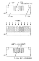
図1(A)に示すのは一般的なIG−FETのソース領域、ドレイン領域およびチャネル形成領域を上面から見た時の状態の模式図である。なお、101がソース領域、102がドレイン領域、103がチャネル形成領域である。
【0041】
そして、本発明の特徴はチャネル形成領域103内にドットパターン状に不純物領域104が形成されている点である。本発明においては、添加する不純物として炭素(C)、窒素(N)、酸素(O)の内、選ばれた一種または複数種類の元素を用いている。
【0042】
添加された不純物はチャネル形成領域103内に局部的にエネルギーバンド幅の大きいエネルギー障壁を形成する。本発明の様に炭素、窒素、酸素を用いた場合には、図14(A)で示す状態であったエネルギーバンドを図14(B)で示す状態とし、エネルギーバンド幅(Eg)を広げることで障壁ΔEがさらに大きな障壁ΔE’となる。例えば、酸素を添加した場合には SiOx で示される様な構造の絶縁性の高抵抗領域となり電気的にも障壁となる。
【0043】
特に、図1(A)に示す様にドレイン領域102とチャネル形成領域103との接合部は最も電界の変化の激しい領域であるので、この位置に不純物領域104を配置しておくことが望ましい。また、ゲイト電極による電界がドレイン領域102内にもおよぶ場合はドレイン領域102内に不純物領域104を形成することも可能である。逆にソース領域101内には不純物領域104は形成しない方が好ましい。
【0044】
この様に、炭素、窒素、酸素を用いる場合においては、どの場合も不純物領域を絶縁性のエネルギー障壁として活用するのでNチャネル型FETとPチャネル型FETとで共通化することができる。このことは、本発明をCMOS回路に適用した場合に製造工程を簡略する上で有利であることを意味する。
【0045】
また、これらの不純物元素は、母体基板がシリコンである場合、シリコン原子と強く結合するので加熱処理などにより再拡散する恐れが少ない。
【0046】
また、本発明は 0.2μm以下といったディープサブミクロン領域の微細加工を必要とする微細素子を形成する際に極めて効果的である。従って、チャネル形成領域の長さ(チャネル長またはソース/ドレイン間距離)も0.01〜1.0 μm、代表的には0.01〜0.35μmといった短いものとなるため、不純物領域はさらに細かいパターンを切らなければならない。
【0047】
例えば、ドットパターン状の不純物領域を形成する際にレジストマスクを利用する場合にはレジストマスクに開孔を設けるパターニングは解像度の問題から通常の露光法を用いることができない。その様な場合においては、パターニングを電子描画法や FIB法を用いて行うことで微細パターンを実現すれば良い。
【0048】
また、このドットパターン状の不純物領域はパターニングにより人為的に配列して形成されるので、図1(A)の様な配置だけでなく、任意の様々な配置とすることが可能である。
【0049】
次に、図1(A)に示すソース領域/チャネル形成領域/ドレイン領域の構成を有する絶縁ゲイト型半導体装置(IG−FET)を駆動させた際に、どの様にして短チャネル効果が抑制されるかを以下に説明する。
【0050】
まず、図1(A)をA−A’で切った断面図を図1(B)に示す。105はフィールド酸化膜、106はチャネルストッパーである。不純物領域104の形状は条件設定によって様々なバリエーションを採りうるが、ここでは理想的に散乱がないものとして棒状に注入された場合を例にする。
【0051】
また、図1(A)をB−B’で切った断面図を図1(C)に示す。107はフィールド酸化膜である。通常、フィールド酸化膜の下にはチャネルストッパーが配置されるがここでは略記する。また、ある不純物領域104の幅はwpi,nで表され、その間隔はwpa,mで表される。ここで、n,mはチャネル形成領域103内において、wpi,nがn番目の不純物領域の幅であり、wpa,mがm番目の不純物領域間の間隔(キャリアの移動するパス)であることを意味している。
【0052】
ここまでの説明は単に構造についての説明であったが、次にその効果についての説明を行う。まず、図1(B)に示す様な構造を有する半導体装置に対してゲイト電圧、ドレイン電圧を印加した場合には、図2(A)に示す様な状態でソース側空乏層201、チャネル側空乏層202、ドレイン側空乏層203が形成される。即ち、ドレイン側空乏層203は不純物領域204が障壁となってソース側への広がりを防止された形となる。
【0053】
図1(B)では判りにくいが不純物領域204は図1(A)に示す様に配置されているので、チャネル形成領域を塞ぐ格子状のフィルターでドレイン側空乏層の広がりを抑えているというモデルで考えれば理解しやすい。
【0054】
従って、本発明による構造の半導体装置においては、図2(A)に示す様に空乏層が実質的に相互に干渉することなく分断される。即ち、ソース側空乏層201、チャネル側空乏層202が、ドレイン側空乏層203の影響を受けないで分布することになるので、エネルギー状態は図2(B)に示す状態となる。
【0055】
即ち、図5に示した従来のエネルギー状態図と異なり、チャネル領域のエネルギー状態は殆どゲイト電圧による電界のみに制御されるので、チャネル領域に対して概略平行な形状を有する。従って、短チャネル効果特有のパンチスルー現象の様な問題がなく、ドレイン耐圧の高い半導体装置を構成することができる。
【0056】
さらに、図2(A)に示す様に、本発明においては空乏層の占める体積が、図3に示した様な従来のものと比べて減少しているため、従来よりも空乏層電荷が小さく、空乏層容量が小さい特徴がある。ここで、S値を導出する式は次式で表される。
【0057】
【数3】

即ち、前述の様に、図5に示すグラフにおいて501で示される領域における傾きの逆数を表していることが判る。また、数3の式は近似的に次式の様に表すことができる。
【0059】
【数4】
数4において、kはボルツマン定数、Tは絶対温度、qは電荷量、Cd は空乏層容量、Citは界面準位の等価容量、Coxはゲイト酸化膜容量である。従って、本発明によれば空乏層容量Cd が従来よりも十分小さくなるので、S値を85mV/decade 以下(好ましくは70mV/decade 以下) の小さな値とすることができる、即ち優れたサブスレッショルド特性を得ることができるのである。
【0061】
また、本発明が目指すところは、空乏層容量Cd および界面準位の等価容量Citを0に可能な限り近づけることである。即ち、Cd =Cit=0となる理想状態におけるS値(60mV/decade )に近づけることにある。
【0062】
また、チャネル形成領域が図1(C)に示す構造となっていることは短チャネル効果によるしきい値電圧の低下を緩和する上で非常に重要である。なぜならば、図1(C)に示す構造が意図的に狭チャネル効果を生み出すために必要な構成だからである。
【0063】
例えば、図1(C)に示す様にある断面に着目すると、チャネル形成領域の幅Wは不純物領域104によって分断され、実質的に狭いチャネル幅wpa,mを持つ複数のチャネル形成領域の集合体と見なすことができる。
【0064】
即ち、その複数の狭いチャネル幅wpaを有する領域において狭チャネル効果が得られるのである。マクロ的に見ると図1(A)に示す様にチャネル形成領域全体にこの様な狭チャネル効果が得られる領域が存在するので、全体的にも狭チャネル効果が得られ、しきい値電圧が増加すると考えられる。
【0065】
従って、チャネル長に短くなることで短チャネル効果によってしきい値電圧が低下したとしても、以上の理由により狭チャネル効果によってしきい値電圧を意図的に増加させてしきい値制御を行うことができるので、結果的にしきい値電圧の変化を緩和することが可能となる。
【0066】
また、他の発明の構成は、
結晶半導体を利用して形成されたソース領域、ドレイン領域およびチャネル形成領域を形成する工程と、
前記チャネル形成領域上にゲイト絶縁膜およびゲイト電極とを形成する工程と、
を少なくとも有する絶縁ゲイト型半導体装置の作製方法であって、
前記チャネル形成領域に対してキャリアが移動する領域と、
前記ドレイン領域より前記チャネル形成領域およびソース領域に向かって広がる空乏層をピニングするための不純物領域と、
を人為的かつ局部的に形成する工程を少なくとも有することを特徴とする。
【0067】
また、他の発明の構成は、
結晶半導体を利用して形成されたソース領域、ドレイン領域およびチャネル形成領域を形成する工程と、
前記チャネル形成領域上にゲイト絶縁膜およびゲイト電極とを形成する工程と、
を少なくとも有する絶縁ゲイト型半導体装置の作製方法であって、
前記チャネル形成領域に対してキャリアが移動する領域と、
不純物元素の添加により所定のしきい値電圧に制御するための不純物領域と、
を人為的かつ局部的に形成する工程を少なくとも有することを特徴とする。
【0068】
また、他の発明の構成は、
結晶半導体を利用してソース領域、ドレイン領域およびチャネル形成領域とを形成する工程と、
前記チャネル形成領域において人為的かつ局部的に不純物領域を形成する工程と、
前記チャネル形成領域上にゲイト絶縁膜およびゲイト電極とを形成する工程と、
を少なくとも有する絶縁ゲイト型半導体装置の作製方法において、
前記不純物領域にはエネルギーバンド幅(Eg)を広げる不純物元素が人為的かつ局部的に添加されていることを特徴とする。
【0069】
また、他の発明の構成は、
結晶半導体を利用して形成されたソース領域、ドレイン領域およびチャネル形成領域を形成する工程と、
前記チャネル形成領域上にゲイト絶縁膜およびゲイト電極とを形成する工程と、
を少なくとも有する絶縁ゲイト型半導体装置の作製方法であって、
前記ドレイン領域より前記チャネル形成領域およびソース領域に向かって広がる空乏層をピニングするための不純物領域を形成するために、前記チャネル形成領域に対してエネルギーバンド幅(Eg)を広げる不純物元素を人為的かつ局部的に添加する工程を有することを特徴とする。
【0070】
また、他の発明の構成は、
結晶半導体を利用して形成されたソース領域、ドレイン領域およびチャネル形成領域を形成する工程と、
前記チャネル形成領域上にゲイト絶縁膜およびゲイト電極とを形成する工程と、
を少なくとも有する絶縁ゲイト型半導体装置の作製方法であって、
不純物元素の添加により所定のしきい値電圧に制御するための不純物領域を形成するために、前記チャネル形成領域に対してエネルギーバンド幅(Eg)を広げる不純物元素を人為的かつ局部的に添加する工程を有することを特徴とする。
【0071】
また、他の発明の構成は、
結晶半導体を利用してソース領域、ドレイン領域およびチャネル形成領域とを形成する工程と、
前記チャネル形成領域においてエネルギーバンド幅(Eg)を広げる不純物元素を添加することにより、人為的かつ局部的に不純物領域を形成する工程と、
前記チャネル形成領域上にゲイト絶縁膜およびゲイト電極とを形成する工程と、
を少なくとも有する絶縁ゲイト型半導体装置の作製方法において、
前記不純物領域は絶縁性を有しており、
前記チャネル形成領域において前記不純物領域以外の領域には前記不純物元素が添加されない又は極微量に添加されていることを特徴とする。
【0072】
【発明の実施の形態】
図1において、ソース領域101、ドレイン領域102とで挟まれた領域がチャネル形成領域103である。本発明は、チャネル形成領域103に対して人為的、かつ、局部的に不純物を添加して不純物領域104を形成する。
【0073】
また、不純物領域104はドットパターン状の形状を有し、規則性をもって配列される。本発明では不純物領域に添加する不純物として炭素、窒素、酸素から選ばれた一種または複数種類の元素を用いるので、絶縁性を有する不純物領域をキャリアが通過することはない。即ち、不純物領域間にのみチャネル領域が形成され、そこをパスとしてキャリアの移動が行われる。
【0074】
以上の様な構成とした半導体装置を駆動させた場合、ドレイン領域102近傍に形成されるドレイン側空乏層は不純物領域104に食い止められて横方向(チャネル形成領域下)に広がらない。即ち、ソース領域101およびチャネル形成領域103近傍のエネルギー状態(電位状態)がドレイン側空乏層に影響されないので、それぞれの電界は実質的には独立に形成される。
【0075】
従って、いわゆる短チャネル効果に起因するパンチスルー現象やサブスレッショルド特性の劣化がなく、高いドレイン耐圧を実現することができる。
【0076】
また、不純物領域104は実質的にチャネル幅を狭くしており、不純物領域104同士の間においてはいわゆる狭チャネル効果が生じる。従って、短チャネル効果に起因するしきい値電圧の低下を、狭チャネル効果に起因するしきい値電圧の増加によって緩和もしくは相殺することが可能である。
【0077】
以上の構成でなる本発明について、以下に記載する実施例でもって詳細な説明を行うこととする。
【0078】
【実施例】
〔実施例1〕
本発明を用いて単結晶シリコン(珪素)基板上に絶縁ゲイト型電界効果トランジスタを形成する例を図7を用いて説明する。なお、本実施例では説明を簡略化するためP型シリコン基板上に単体のNチャネル型FETを形成する場合の例を示す。
【0079】
まず、701はP型シリコン基板であり、その上にはパッド酸化膜として酸化珪素膜702、さらにその上には後に選択酸化の際のマスクとして機能する窒化珪素膜703を形成する。酸化珪素膜702および窒化珪素膜703の膜厚は500 〜2000Åもあれば良い。(図7(A))
【0080】
次に、パターニングにより素子形成領域のみに窒化珪素膜703を残し、その状態でP型を付与する不純物元素のイオン注入を行い、さらにその後、1000〜1100℃の温度でウェット酸化を行う。
【0081】
この工程により露出したシリコン表面は選択的に熱酸化され、図7(B)に示す様にフィールド酸化膜704が形成される。フィールド酸化膜704は素子同士を絶縁分離する機能を有する。
【0082】
また、前述のイオン注入工程により注入されたP型を付与する不純物元素(B)はフィールド酸化膜704の下にチャネルストッパー705を形成する。これは、フィールド酸化膜704下にチャネルが形成されない様にするための領域であり、通常、母体となる基板(本実施例ではP型シリコン基板)と同じ導電性を持たせる。
【0083】
そして、窒化珪素膜703、酸化珪素膜(パッド酸化膜)702を除去して図7(B)に示す状態が得られる。この様な選択酸化工程に際してはLOCOS法、PLANOX法、Isoplanar法、SWAMI法などの様々な選択酸化方法を用いることが可能である。
【0084】
次に、チャネル形成領域706に対して炭素、窒素、酸素から選ばれた一種または複数種類の元素を添加し、空乏層のストッパーとなる不純物領域707を形成する。不純物元素を添加する領域707はパターニングにより図示しないレジストに開孔を設けて選択的に設計すれば良い。
【0085】
なお、不純物領域707をドットパターン状にするためには極めて微細なリソグラフィ技術を必要とする。そのためには、電子ビームを用いる技術(電子描画法)やイオンビームを用いる技術(FIB 法) を用いてドットパターン形状の露光を行えば良い。
【0086】
この時、不純物領域707同士の間隔wpa,mはそれぞれ揃えることが望ましい。なぜならば、しきい値電圧のバラツキ(狭チャネル効果のバラツキに起因する)や発熱のバラツキ(不純物領域間を流れる電流密度のバラツキに起因する)を生じる恐れがあるからである。
【0087】
不純物の添加が終了したら、熱酸化処理を行い100 〜500 Åの熱酸化膜708を形成する。この熱酸化処理により形成された薄い熱酸化膜708はそのままゲイト絶縁膜として機能する。
【0088】
さらに、チャネル形成領域706において酸化膜708上にゲイト電極としてポリシリコン膜709を形成する。ゲイト電極709は成膜する段階で予め不純物元素を添加しておいて導電性を持たせれば良い。こうして図7(C)に示す状態が得られる。
【0089】
その後、図7(D)に示す様に、N型を付与する不純物元素(PまたはAs)を添加し、自己整合的にソース領域710、ドレイン領域711を形成する。その後、ゲイト電極709を覆う様にして窒化珪素膜を3000Åの厚さに成膜し、エッチバック法を用いてゲイト電極709の側面のみにサイドウォール712を残存させる。
【0090】
次に、この状態で全面にスパッタ法によりチタン膜を成膜し、加熱、レーザーアニール、ランプアニールなど手段のよるシリサイド形成を行う。この工程により、ソース領域710およびドレイン領域711の表面ならびにゲイト電極709の表面にはチタンシリサイド713〜715が形成される。チタンシリサイド713〜715は極めて低抵抗であるので、後に形成する配線とのオーミック接触を確保する上で好ましい。
【0091】
シリサイド形成が終了したら、層間絶縁膜として窒化珪素膜716を成膜し、コンタクトホールを形成してソース電極717、ドレイン電極718を形成する。こうして図7(E)に示す様な構造のIG−FETが完成する。
【0092】
本発明ではIG−FETのチャネル形成領域にドットパターン状に不純物領域を形成することに特徴があるが、ドットパターンの形成箇所はある範囲の条件を満たす必要がある。そのことについて、図8を用いて以下に記載する。
【0093】
図8において、801はチャネル形成領域の一部を示している。チャネル幅はWである。ここで、チャネル幅Wの内、ドットパターン802が占有している幅をW pi, n と定義する。W pi, n の値としては例えば10〜100 Åもあれば十分である。また、任意のドットパターン802の幅をwpi,1、wpi,2、wpi,3・・・wpi,nとすると、Wpiは次式で表される。
【0094】
【数1】
但し、本発明の構成を達成するためにはチャネル形成領域の端部以外の領域に、不純物領域が少なくとも一つ形成されている必要があるのでnは1以上の整数である。
【0096】
また、チャネル幅Wの内、ドットパターン間の領域(キャリアの移動するパス)803が占有している幅をW pa, m と定義する。W pa, m の値としては例えば100 〜3000Å(代表的には500 〜1500Å)とすることができる。また、任意のドットパターン間の領域803をwpa,1、wpa,2、wpa,3・・・wpa,mとすると、Wpaは次式で表される。
【0097】
【数2】
但し、前述の様にチャネル形成領域の端部以外の領域に不純物領域が少なくとも一つ形成されているので、チャネル形成領域は少なくとも2分されてmは2以上の整数となる。
【0099】
即ち、全チャネル幅WはW=Wpi+Wpa、かつ、n+mは3以上という関係が成り立っている。そして、WとWpi、WとWpaおよびWpiとWpaとの関係は、同時に以下の条件を満たすことが望ましい。
Wpi/W=0.1 〜0.9
Wpa/W=0.1 〜0.9
Wpi/Wpa=1/9 〜9
【0100】
これらの数式の意味するところは、Wpa/WまたはWpi/Wが0または1であってはならないという事である。例えば、Wpa/W=0(Wpi/W=1と同義)の場合、図8(B)に示す様にチャネル形成領域を完全に不純物領域で塞いでしまうので電流の流れるパスが存在しない状態となる。
【0101】
逆にWpa/W=1(Wpi/W=0と同義)の場合、図8(C)に示す様にチャネル形成領域に不純物領域が全く存在しないのでドレイン側空乏層の広がりを抑えることができない。
【0102】
以上の理由により、Wpa/WおよびWpi/Wの関係式は0.1 〜0.9 (好ましくは0.2 〜0.8 )の範囲に収まり、また、同時にWpi/Wpa=1/9 〜9 を満たすことが望ましい。なお、チャネル長をLとすると、チャネル形成面積はW×Lで表される。
【0103】
また、本発明はFETの性能を示す代表的なパラメータである移動度の向上に効果的である。その理由について以下に説明する。
【0104】
移動度は半導体(本実施例ではシリコン基板)中のキャリアの散乱によって決まるが、シリコン基板における散乱は格子散乱と不純物散乱とに大別される。格子散乱はシリコン基板中の不純物濃度が低く、比較的高温で支配的であり、不純物散乱は不純物濃度が高く、比較的低温で支配的である。これらが影響し合って形成される全体的な移動度μは次式で表される。
【0105】
【数5】
この数5で示される式は、全体的な移動度μが、格子散乱の影響を受けた場合の移動度μl ( lはlattice を意味する) の逆数および不純物散乱の影響を受けた場合の移動度μi ( iはimpurityを意味する) の逆数の和に反比例することを意味している。
【0107】
ここで、格子散乱ではドリフト電界がそれほど強くなければ音響フォノンが重要な役割を果たし、その時の移動度μl は、次式の様に温度の-3/2乗に比例する。従って、キャリアの有効質量(m*)と温度(T)で決まってしまう。
【0108】
【数6】
また、不純物散乱による移動度μi は、次式の様に温度の3/2 乗に比例し、イオン化した不純物の濃度Ni に逆比例する。即ち、イオン化した不純物の濃度Ni を調節することで変化させることができる。
【0110】
【数7】
これらの式によると、従来の様にチャネル形成領域全体に不純物を添加するチャネルドープでは不純物散乱の影響を受けて移動度を稼ぐことができない。しかしながら、本発明では局部的に不純物領域を形成しているので、隣接する不純物領域の間(Wpaの幅を持つ領域) には不純物が添加されない。
【0112】
即ち、理論的には数7においてイオン化した不純物の濃度Ni を限りなく0に近づけることを意味するため、移動度μi は限りなく無限大に近づいていくことになる。即ち、数5において1/μi の項を無視することができる程度にまで不純物を減少させることを意味するので全体の移動度μは限りなく移動度μl に近づいていく。
【0113】
また、キャリアの有効質量(m*)を小さくすることで移動度μl をさらに大きくすることも理論的には可能である。これは極低温の領域において、キャリア(特に電子の場合)の有効質量が結晶軸の軸方位に依存して変化する現象を利用することで成しうる。
【0114】
文献によれば、ソース/ドレイン間を結ぶチャネル方向(キャリアの移動する方向)が単結晶シリコンの<100>軸方向と一致する様に構成した時、最小の有効質量を得ることができる。
【0115】
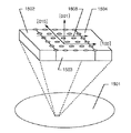
例えば、図15に示す様に、(100)面を有する単結晶シリコン基板1501上にソース領域1502、チャネル形成領域1503、ドレイン領域1504が形成されているとする。この時、チャネル方向1505を[100]とした場合の様な時がこれに相当する。但し、この例は4°Kという極低温領域における結果である。
【0116】
また、結晶格子間をうまくキャリアがすり抜けて行ける様に、チャネル方向および不純物領域707の軸方向(配列方向)と、結晶格子の軸方向とを概略平行(軸方向のずれを±10°以内に収める)にさせることが望ましい。単結晶ならばシリコン原子は規則正しく配列しているので、結晶格子の配列方向と平行に移動するキャリアは格子散乱の影響を殆ど受けないで済む。
【0117】
例えば、単結晶シリコン基板において上記の様な方向における回転軸を0°とすると、他にも90°、180°、270°の回転軸の場合において同様の効果を得ることができる。
【0118】
以上の様に、チャネル形成領域を移動するキャリアはチャネル形成領域内に存在する不純物領域以外の領域を通る。この様子を図16の模式図を用いて簡単に説明する。
【0119】
図16(A)において、1601で示されるのはチャネル形成領域である。即ち、図16(A)はチャネル形成領域を右斜め上方から見た図である。本発明を実施したチャネル形成領域は、立体的には図16(A)の様に不純物領域1602が形成されている。
【0120】
図16(A)に記載された矢印1603はキャリア(電子または正孔)の進行方向を示すものである。図16(A)に示す様にチャネル形成領域1601内には複数の不純物領域1602が配置されており、キャリアはそれら不純物領域1502以外の領域を通過する。
【0121】
キャリアの進行方向をチャネル形成領域1601の上面から見ると図16(B)の様に見える。図16(B)は図16(A)において、ACEFで表される面を見た図である。この図16(B)を見ると、キャリアが不純物領域1602を避け、不純物散乱のない領域を移動していることが判る。
【0122】
即ち、大部分のキャリアは矢印で示す様に、不純物領域1602の間を通ってソース/ドレイン間を移動する。勿論、不純物領域を避ける様にしてジグザグに移動する場合も含まれる。
【0123】
また、図16(C)に示すのは、チャネル形成領域1601を側面から見た図である。なお、図16(C)は図16(A)において、ABCDで表される面を見た図である。また、1603で示されるのは矢印であり、紙面に向かって手前方向に矢先が向いていることを示している。この図からもキャリアが不純物領域1602の間を移動することが判る。
【0124】
〔実施例2〕
本実施例では、本発明を利用してNチャネル型FET(NMOS)とPチャネル型FET(PMOS)とを相補的に組み合わせたCMOS回路を構成する場合の例を示す。CMOS回路の作製工程の詳細についてはここでは省略するが、本発明では実施例1で説明した様に、ゲイト絶縁膜を形成する前にチャネル形成領域のみにドットパターン状の不純物領域を形成する。
【0125】
図13(A)に本発明を利用した場合におけるCMOS回路の断面を示す。図13(A)は一般的な作製方法で形成されたCMOS回路をチャネル方向で分断した断面図である。
【0126】
図13(A)において、1301はN型シリコン基板、1302はnウェル、1303はpウェルである。つまり、nウェル1302上にPチャネル型FET(PMOS)、pウェル1303上にNチャネル型FET(NMOS)が形成される。
【0127】
NMOSおよびPMOSはそれぞれ選択酸化法で形成されたフィールド酸化膜1304で分離され、pウェル側のフィールド酸化膜の下にはチャネルストッパー1305が配置される。
【0128】
また、nウェル1302にはP型を付与する不純物、例えばボロンが添加されてPMOSのソース領域1306、ドレイン領域1307が配置されている。また、pウェル1303にはN型を付与する不純物、例えばリンや砒素が添加されてNMOSのドレイン領域1308、ソース領域1309が配置されている。
【0129】
また、ソース領域1306、ドレイン領域1307およびソース領域1308、ドレイン領域1309で挟まれたチャネル形成領域には、予めゲイト絶縁膜1310を形成する前にドットパターン状の不純物領域1311、1312を形成しておく。
【0130】
本実施例でゲイト絶縁膜1310の形成前に不純物領域1311、1312を形成する理由は、ゲイト絶縁膜1310とチャネル形成領域との界面に損傷を与えないためであるが、ゲイト絶縁膜1310を通して不純物を添加する方法をとることも可能である。
【0131】
なお、本実施例では不純物領域1311、1312を形成するにあたって酸素を用いるので、NMOSとPMOSとで使い分ける必要はなく、共通化することができる。
【0132】
また、本実施例の様なCMOS回路を構成する場合、図13(A)に示す様にドレイン領域1307、1308内にも不純物領域1311、1312を形成しておくことが望ましい。
【0133】
なお、例えば本発明の半導体装置を画素などの様にソースとドレインが入れ替わる様な素子に用いる時はソース領域とドレイン領域の双方の内に不純物領域を形成すれば良い。
【0134】
そして、チャネル形成領域の上に導電性材料でなるゲイト電極1313、1314を形成し、それを覆う様にして層間絶縁膜1315が成膜される。さらに、層間絶縁膜1315にコンタクトホールを形成して、PMOSのソース電極1316、PMOSおよびNMOSの共通ドレイン電極1317、NMOSのソース電極1318を配置する。
【0135】
図13(A)に示す構造のCMOS回路は本発明により短チャネル効果を問題としないで微細化することができるので、極めて集積度の高い集積化回路を構成しうる。
【0136】
また、図13(A)に示したCMOS回路とバイポーラトランジスタとを組み合わせたBiCMOS回路を構成することも可能である。本発明を利用して形成したBiCMOS回路の例を図13(B)に示す。
【0137】
図13(B)において、1319はP型シリコン基板であり、1320は埋め込みN+ 領域、1321はエピタキシャル成長により形成されたpウェルであり、埋め込みN+ 領域1320上のpウェル1321はN型にドーピングされてコレクタとして機能するnウェル1322となっている。また、1323は埋め込みN+ 領域1320からの取り出し電極となるDeepN+ 領域である。
【0138】
1324は通常の選択酸化法で形成されたフィールド酸化膜であり、pウェル1321にはn+ 領域1325、nウェル領域1322にはp+ 領域1326が形成されている。なお、バイポーラトランジスタを構成する側のnウェル1322には活性ベースとなるp- 領域1327がまず形成され、次いで外部ベースとなるp+ 領域1328、n+ 領域1329が配置される。
【0139】
なお、PMOS側およびNMOS側の両方には不純物領域1330が配置される。不純物領域1330は上記n+ 領域やp+ 領域を形成した後に形成しても良いし、その前であっても良い。勿論、炭素、窒素、酸素のいずれを用いるのであっても構わない。
【0140】
そして、ゲイト電極1331、層間絶縁膜1332、ソース/ドレイン配線1333を配置してBiCMOS回路を構成する。BiCMOS回路はバイポーラトランジスタの高速動作性とCMOS回路の低消費電力性を有効に併用するための回路構成である。
【0141】
〔実施例3〕
実施例1では不純物領域707の深さ方向の形状を棒状に記載したが、これは注入時に散乱が全くない場合の様な理想状態であって、実際にはイオン注入の条件によって様々な形状の不純物領域を形成することも可能である。
【0142】
例えば、イオン注入の条件によっては図9(A)に示す様なクサビ状の不純物領域901が形成されることもありうる。また、逆に図9(B)に示す様なシズク状の不純物領域902が形成されることもありうる。特に、図9(B)に示した様な形状とした場合、不純物領域902の下部で隣接する不純物領域同士が互いに接触する状態となる。
【0143】
この状態では、実質的にチャネル形成領域がバルク基板と絶縁分離されたSOI構造と見なせる様になる。この構造はドレイン側空乏層がチャネル形成領域の空乏層に影響を与えるのを極めて効果的に抑制することができる。また、チャネル形成領域の空乏層が下方へ広がるのを防ぐ効果も期待できる。
【0144】
〔実施例4〕
実施例1では図1(A)に示した様なマトリクス状にドットパターン(不純物領域)を配置する例を示したが、設計パターンを変えることで他の様々な配置パターンとすることができる。
【0145】
例えば、図10(A)に示す様に、不純物領域1001が交互にかみ合う様に配置したパターンとすることもできる。この場合、ドットパターン間の隙間を次の列で補う構成となるので、ドレイン側空乏層の横方向への広がりを効果的に防止することができる。特に、チャネル長が0.1 μm以下となった場合の様に短チャネル効果の影響が極めて大きくなる様なIG−FETにおいて非常に効果的な構成である。
【0146】
ただし、キャリアの移動する経路が点線で示した様に蛇行する様になるので、キャリアの移動距離が長くなる分、移動度が低下する可能性もある。しかし、この構造が効果を発揮するチャネル長0.1 μm以下の領域では、ソース領域からでたキャリアが一瞬でドレイン領域に到達するので、実質的には多少移動距離が長くなっても問題とならないと考えられる。
【0147】
従って、例えばチャネル長が0.1 μm以上の場合には図1(A)に示した様にドットパターン状不純物領域を配置し、チャネル長が0.1 μm以下の場合には図10(A)に示した様に配置することが望ましい。
【0148】
また、図10(B)に示す様に、ドットパターンをチャネル方向と垂直な楕円形または長方形とすることもできる。この場合、ドレイン側空乏層を抑制するには適した構成となるが、キャリアの移動を妨げる可能性もあるため、例えば0.2 μm以下に非常にチャネル長に短い半導体装置に利用することが好ましい。
【0149】
また、図10(C)に示す様に、ドットパターンをチャネル方向と平行な楕円形または長方形とすることもできる。この場合、狭チャネル効果がより顕著に現れる構成となるので、しきい値電圧を多めに増加させることが必要な時に効果的な構成と言える。
【0150】
〔実施例5〕
本発明は実施例1で示した様な横形IG−FETだけでなく、さらに様々な構造のIG−FETに対しても適用することができる。例えば、横形IG−FETには他にもLDD(オフセット)構造(図11(A))、2重ドレイン構造(図11(B))、埋め込みチャネル構造(図11(C))、SOI構造(図11(D))、SIMOX構造(図11(E))などがある。
【0151】
本実施例では、Nチャネル型FETを例にとり、上記構造に応用した場合について説明する。なお、図中のN+、N−はN型導電性の強弱を相対的に示したもので、N+はN−よりも強いN型導電性を有していることを意味している。
【0152】
図11(A)はソースまたはドレイン領域1101とチャネル形成領域1102との間に低濃度不純物領域1103を配置した構造である。低濃度不純物領域1103が存在する分、ドレイン側空乏層はなだらかに広がりやすいが、本発明によりその広がりを抑制することができる。
【0153】
また、図11(B)はソースまたはドレイン領域1104の側面に0.1 〜0.5 μm幅の導電性領域1105を形成した構造である。ソースまたはドレイン領域1104と導電性領域1105は同じ導電性であり、導電性領域1105の方が導電性は弱い。例えば、ソースまたはドレイン領域1104をAs(砒素)を注入して形成し、弱い導電性領域1105をP(燐)を注入して形成することで構成することができる。
【0154】
図11(C)に示す埋め込みチャネル構造はNチャネル型FETとPチャネル型FETとでCMOS回路を構成する様な時に結果的に形成される構成である場合が多く、短チャネル効果も影響を受けやすい構造である。
【0155】
構造的には、例えばNチャネル型FETにおいて、チャネル形成領域の界面付近にソース/ドレイン領域1106と同一かつ弱い導電性領域1107を形成して構成される。
【0156】
従って、この導電性領域1107の直下にチャネルが形成されるのであるが、この様な場合においても本発明を実施することで短チャネル効果を抑制し、パンチスルー現象やしきい値電圧の低下を防止することができる。
【0157】
また、SOI構造は素子として使用する半導体層を薄膜化して空乏層を低減する目的も含めて開発された技術であるからそれ自体短チャネル効果を抑制する効果を持っている。例えば、図11(D)に示す構造は一般的にSOS(silicon-on-sapphire )構造と呼ばれ、サファイア基板1108上にシリコン単結晶を成長させて形成される。
【0158】
しかし、1μm以下の単結晶シリコン層を形成するのは困難であり、空乏層の広がりを抑えるにも限界がある。従って、本発明をSOI構造に応用すればより確実に短チャネル効果を防止することが可能となる。
【0159】
なお、同じSOI構造の部類に含まれるが一般的にSIMOX(separation-by-implanted oxygen)と呼ばれる基板上にIG−FETを形成した例が図11(E)である。この場合、単結晶シリコン基板1109に対して酸素を注入することによって埋め込み酸化層1110を形成する。また、酸素の注入深さを浅くすることで極めて薄い単結晶薄膜を形成することができる。
【0160】
この様な場合においても、本発明を用いることは可能である。この場合、ドレイン側空乏層がチャネル形成領域へと広がるのを抑止する(ピニングする)効果を期待することができる。
【0161】
〔実施例6〕
本発明においてチャネル形成領域に不純物領域を形成する手段として、レジストマスクを用いたパターニングによる方法以外にも、不純物が歪みに偏析する性質を利用する方法も可能である。
【0162】
まず、実施例1の手順に従って図7(B)と同じ状態を得る。即ち、図12(A)において、1201はシリコン基板、1202はフィールド酸化膜、1203はチャネルストッパーである。
【0163】
この状態において、集束イオンビーム等を利用してシリコン基板表面の局部的な異方性エッチング加工を行い、溝状または穴状パターン1204を所望の位置に所望の形状で描画する。(図12(A))
【0164】
次に、不純物元素、例えば窒素を基板1201全面に添加する。勿論、炭素や酸素であっても構わない。この不純物元素は後に不純物領域を形成するためのものである。また、注入深さは溝状または穴状パターン1204の深さよりも深いことが望ましい。(図12(B))
【0165】
不純物元素の添加が終了したら、次に1000〜1200℃前後の高温で加熱処理を行う。この加熱処理により溝状または穴状パターン1204の側壁には熱酸化膜1205が形成され、溝状または穴状パターン1204は埋め込まれる。従って、この領域は実質的に SiOx で表される様な酸化物領域1205となる。この場合、加熱処理を酸化性雰囲気で行うと酸化物領域1205の形成速度が増加することので好ましい。
【0166】
そして、同時にシリコン基板1201全体に添加されていた不純物元素が酸化物領域1205に偏析する。これは、酸化物領域の近傍に発生した大きな歪みや格子欠陥等に不純物元素が偏析するために生じる。
【0167】
以上の様な過程を経ることで、酸化物領域1205の周辺部は不純物元素が偏析して不純物領域1206となる。
【0168】
また、単結晶シリコン基板1201中にリンやボロンといった一導電性を付与する不純物元素が添加されている場合、酸化物領域1205を構成する熱酸化膜が形成される際に、ボロンは熱酸化膜中に取り込まれ、リンは酸化膜/シリコン界面に排斥される(パイルアップする)傾向にある。
【0169】
この様な効果をうまく利用することで、不純物散乱による移動度の低下を効果的に抑制することも可能である。
【0170】
また、例えば、集束イオンビームの様なマスクレスでイオン注入を行うことができる装置を用いて、直接単結晶シリコン基板上に酸素イオンを注入し、加熱処理を行うことでイオン注入した領域を酸化物領域に変成させることも可能である。集束イオンビーム以外にも電子ビーム等を用いても良い。
【0171】
〔実施例7〕
本実施例では、本発明を利用した半導体装置を製品(電子機器)に組み込んだ場合の一例を示す。ここでは、ノート型パソコンに組み込まれたIC回路を例にとって説明する。説明は図17を用いて行う。
【0172】
図17において、3001は本体、3002はフタ部、3003はキーボード、3004は画像表示部であり、本体3001内には様々な集積回路3005が組み込まれている。
【0173】
集積回路3005を取り出してみると、外部はパッケージ3011で覆われて内部の半導体チップは樹脂等で保護されている。また、内部の半導体チップはリード3012によって外部と接続される。通常、目にする集積回路(ICチップ)3005は、外目には黒色のパッケージ3011とリード3012しか見えないので完全にブラックボックスとなっている。
【0174】
そのパッケージ3011で保護された半導体チップを取り出して見ると、例えば次の様な構成となっている。まず、基板3013上には演算部(プロセッサー)3014とメモリ部3015が配置されている。なお、3016は半導体素子とリード3012とを接続するボンディング部である。
【0175】
演算部3014、メモリ部3015はCMOS回路、BiCMOS回路、DRAM回路、SRAM回路など、他にも様々な回路を用いて構成さえている。本実施例で示した図15の様な構成は、同一基板上に演算部3014とメモリ部3015が配置されていることに特徴がある。
【0176】
この様に演算部3014とメモリ部3015とが隣接した構成とすると、演算部3014とメモリ部3015との間のデータのやりとりが非常に高速で行われる様になるため、動作速度の速い回路を形成することが可能となる。
【0177】
また、ワンチップ上に必要な回路を全て集積化することも可能であるので、製造コストを大幅に低減することも期待できる。さらには、配置面積を減らすことで製品の小型化を図ることもできる。
【0178】
本発明を利用すれば短チャネル効果を問題とせずに半導体素子の微細化を行うことができるので、上記の様なワンチップ化と併用することで半導体電子機器のさらなる小型化、携帯化が実現できる。
【0179】
〔実施例8〕
本発明は実施例7に示した例以外にも様々な半導体電子機器に応用することが可能である。なぜならば、本発明による半導体装置の電気特性は非常に優れたものであり、これを用いて構成したIC回路は高い周波数特性を実現しうるからである。
【0180】
本発明を利用して形成された半導体素子単体のデバイス特性は非常に優れたものとなり、Nチャネル型FETのしきい値電圧Vth,nは-0.5〜3.0 V、Pチャネル型FETのしきい値電圧Vth,pは-3.0〜0.5 Vの範囲で必要とする駆動電圧に合わせて調節できる。また、S値は60〜85mV/decade 、好ましくは60〜70mV/decade が得られる。
【0181】
また、実施例1で説明した様な理由により高い移動度(1000cm2/Vs以上)を得ることができる。移動度を計算式で求める場合、移動度はチャネル幅Wに反比例するので注意が必要である。本発明を実施する場合、チャネル形成領域においては不純物領域によって少なからずチャネル幅が狭くなっているので、実測チャネル幅Wpaを代入しなければ実際の移動度は得られない。
【0182】
以上の様な優れた電気特性を達しうる本発明の半導体装置でIC回路を構成すると、極めて良好な周波数特性を得ることができる。例えば、本発明の半導体装置を用いて9段のリングオシレータを構成すると、3.3 Vの駆動電圧で2〜10GHzの周波数特性を実現しうる。
【0183】
例えば、高周波電子機器である携帯電話などの様に高い周波数特性を必要とする電子機器に対しても本発明は有効である。携帯電話の入力部等に用いられるIC回路は2GHzの周波数特性を必要とするのであるが、本発明はその様な高周波IC回路に対しても十分に対応することができる。
【0184】
【発明の効果】
本発明を利用することでチャネル長が短くなった場合に生じる短チャネル効果を防止することが可能となる。具体的には、まずドレイン側空乏層がソース領域やチャネル形成領域下に広がるのを、チャネル形成領域に局部的に形成した不純物領域で遮り、チャネル形成領域のエネルギー(電位)状態にドレイン電圧が影響しない構成とする。これによりパンチスルー現象やサブスレッショルド特性の劣化を防止することが可能となる。また、同時に高いドレイン耐圧を実現することができる。
【0185】
また、短チャネル効果の特徴の一つであるしきい値電圧の低下を狭チャネル効果によるしきい値電圧の増加によって抑制することができる。この狭チャネル効果は、チャネル形成領域に局部的に不純物領域を形成するという本発明の構成によって人為的に成しうる効果である。
【0186】
以上の様に、本発明を利用することでチャネル長の短いディープサブミクロン領域における半導体装置においても、短チャネル効果を引き起こすことなく動作させることができる。即ち、IG−FETに代表される半導体装置のより一層の集積化と性能の向上が望める。
【図面の簡単な説明】
【図1】 チャネル形成領域の構成を示す図。
【図2】 チャネル形成領域の構成を示す図。
【図3】 従来の半導体装置を説明するための図。
【図4】 チャネル形成領域のエネルギー状態を示す図。
【図5】 従来の半導体装置の特性を示す図。
【図6】 従来の半導体装置の構成を示す図。
【図7】 絶縁ゲイト型電界効果トランジスタの作製工程を示す図。
【図8】 不純物領域の形成条件を説明するための図。
【図9】 不純物領域の深さ方向の形状を示す図。
【図10】 不純物領域の形状および配置を説明するための図。
【図11】 絶縁ゲイト型電界効果トランジスタの構造を示す図。
【図12】 不純物領域の作製工程を示す図。
【図13】 絶縁ゲイト型電界効果トランジスタの構造を示す図。
【図14】 チャネル形成領域のエネルギー状態を示す図。
【図15】 チャネル形成領域の構成を示す図。
【図16】 チャネル形成領域の構成を示す図。
【図17】 半導体装置の応用例を示す図。
【符号の説明】
101 ソース領域
102 ドレイン領域
103 チャネル形成領域
104 不純物領域(ドットパターン)
105 フィールド酸化膜
106 チャネルストッパー[0001]
[Technical field to which the invention belongs]
The invention disclosed in this specification describes an insulated gate semiconductor device formed using a crystalline semiconductor substrate, for example, a single crystal silicon substrate or an SOI substrate (SIMOX, etc.), particularly an insulated gate field effect transistor (hereinafter simply referred to as IG). -Abbreviated as -FET) and a manufacturing method thereof. In particular, this technique is effective when a microelement having a channel length of 1 μm or less (typically 0.01 to 0.35 μm) is manufactured.
[0002]
Therefore, the present invention can be applied to various semiconductor integrated circuits such as IC, VLSI, and ULSI configured by integrating IG-FETs.
[0003]
[Prior art]
In recent years, integrated circuits such as VLSI have been increasingly miniaturized, and the processing width in the deep submicron region such as the width of the wiring is 0.18 μm or less and further 0.1 μm or less has been required. Yes.
[0004]
Until now, the miniaturization of semiconductor elements has been advanced according to the scaling law, and it has been generally known that the miniaturization brings about the improvement of the characteristics of the integrated circuit. However, when microfabrication is performed in the sub-micron region, a problem that simply does not follow the scaling law occurs.
[0005]
As such a problem, a phenomenon called a short channel effect is typically known. The short channel effect means that as the line width of the gate electrode becomes shorter, that is, as the channel formation region becomes shorter, the charge of the channel formation region is not limited to the gate voltage but also the depletion layer charge of the source / drain region, the electric field and the potential distribution. It is a phenomenon that is caused to become greatly affected.
[0006]
This state is simplified and shown in FIG.
[0007]
Usually, the current flowing through the
[0008]
However, when the drain voltage Vd increases, the depletion layer in the vicinity of the
[0009]
Here, the energy state around the channel formation region when the short channel effect occurs will be described with reference to FIG. 4 is an energy band diagram of the
[0010]
When a sufficiently large drain voltage Vd is applied in this state, the state changes to a state shown by a dotted line in FIG. That is, the depletion layer charge or electric field of the
[0011]
As the influence of such a short channel effect on a semiconductor element, for example, an IG-FET, a decrease in threshold voltage (Vth) and a punch-through phenomenon are well known. It is also known that when the influence of the gate voltage on the drain current is reduced due to the punch-through phenomenon, the subthreshold characteristic is deteriorated.
[0012]
First, the decrease in threshold voltage is a phenomenon that can be seen in the same way for both N-channel and P-channel FETs. The degree of this reduction depends not only on the drain voltage but also on various parameters such as substrate impurity concentration, source / drain diffusion layer depth, gate oxide thickness, and substrate bias.
[0013]
Although lowering the threshold voltage is desirable in terms of reducing power consumption, generally, there is a problem in that frequency characteristics do not increase due to a decrease in driving voltage of an integrated circuit.
[0014]
Therefore, until now, as a means for controlling the threshold voltage, an impurity element that uniformly imparts one conductivity is added to the entire channel formation region, and the threshold voltage is controlled by the addition amount. It was common. However, this method still cannot prevent the short channel effect itself, and a punch-through phenomenon has occurred. In addition, the added impurity scatters carriers, which has been a factor of lowering carrier mobility.
[0015]
Further, the deterioration of the subthreshold characteristic due to the punch-through phenomenon means that the subthreshold coefficient (S value) is increased, that is, the switching characteristic of the FET is deteriorated. Here, the influence of the short channel effect on the subthreshold characteristic is shown in FIG.
[0016]
FIG. 5 is a graph in which the horizontal axis represents the gate voltage Vg and the vertical axis represents the logarithm of the drain current Id, and the reciprocal of the slope (subthreshold characteristic) in the
[0017]
As a result, it can be confirmed that the slope of the characteristic decreases as the channel length decreases, that is, the S value tends to increase. This means that the switching characteristics of the FET deteriorate as the channel length becomes shorter.
[0018]
The above is the explanation of the short channel effect that occurs when the length of the channel formation region of the semiconductor element becomes extremely short. However, when the width of the channel formation region becomes extremely narrow, the phenomenon of the narrow channel effect also occurs. To do.
[0019]
FIG. 6 is a cross-sectional view of a general IG-FET cut along a plane perpendicular to the channel direction (direction connecting the source and drain).
[0020]
[0021]
The narrow channel effect is caused by the biting portion (bird's beak) of the
[0022]
[Problems to be solved by the invention]
In the current semiconductor industry, semiconductor integrated circuits integrated to the limit are required, and the key is how far down to the miniaturization of individual semiconductor elements can be pursued. However, even if a technique for forming a fine pattern in the deep sub-micron region has been developed, the problem of the short channel effect as described above has been a fatal obstacle that prevents miniaturization of the element.
[0023]
The present invention has been made in view of the above problems, and discloses a technique for effectively suppressing the short channel effect accompanying the miniaturization of a semiconductor element. It is another object of the present invention to make it possible to form a fine element in a deep submicron region that has been difficult to realize due to the short channel effect.
[0024]
[Means for Solving the Problems]
The configuration of the invention disclosed in this specification is as follows.
A source region, a drain region, and a channel formation region formed using a crystalline semiconductor;
A gate insulating film and a gate electrode formed on the channel formation region;
An insulated gate semiconductor device having at least
The channel formation region is a region where carriers move,
An impurity region that is artificially and locally formed to pin a depletion layer extending from the drain region toward the channel formation region and the source region;
It is characterized by having.
[0025]
In addition, the configuration of other inventions is as follows:
A source region, a drain region, and a channel formation region formed using a crystalline semiconductor;
A gate insulating film and a gate electrode formed on the channel formation region;
An insulated gate semiconductor device having at least
The channel formation region is a region where carriers move,
An artificially and locally formed impurity region for controlling to a predetermined threshold voltage by addition of an impurity element;
It is characterized by having.
[0026]
In addition, the configuration of other inventions is as follows:
A source region, a drain region, and a channel formation region formed using a crystalline semiconductor;
An impurity region artificially and locally formed in the channel formation region;
A gate insulating film and a gate electrode formed on the channel formation region;
In an insulated gate type semiconductor device having at least
An impurity element that broadens an energy band width (Eg) is added to the impurity region.
[0027]
In addition, the configuration of other inventions is as follows:
A source region, a drain region, and a channel formation region formed using a crystalline semiconductor;
A gate insulating film and a gate electrode formed on the channel formation region;
An insulated gate semiconductor device having at least
The channel formation region is a region where carriers move,
An impurity region that is artificially and locally formed to pin a depletion layer extending from the drain region toward the channel formation region and the source region;
Have
An impurity element that broadens an energy band width (Eg) is added to the impurity region.
[0028]
In addition, the configuration of other inventions is as follows:
A source region, a drain region, and a channel formation region formed using a crystalline semiconductor;
A gate insulating film and a gate electrode formed on the channel formation region;
An insulated gate semiconductor device having at least
The channel formation region is a region where carriers move,
An impurity region that is artificially and locally formed to pin a depletion layer extending from the drain region toward the channel formation region and the source region;
Have
In the region in which the carriers move, means for preventing carrier impurity scattering or means for preventing mobility lowering due to factors other than carrier lattice scattering are provided.
[0029]
In addition, the configuration of other inventions is as follows:
A source region, a drain region, and a channel formation region formed using a crystalline semiconductor;
A gate insulating film and a gate electrode formed on the channel formation region;
An insulated gate semiconductor device having at least
The channel formation region is a region where carriers move,
An artificially and locally formed impurity region for controlling to a predetermined threshold voltage by addition of an impurity element;
Have
An impurity element that broadens an energy band width (Eg) is added to the impurity region.
[0030]
In addition, the configuration of other inventions is as follows:
A source region, a drain region, and a channel formation region formed using a crystalline semiconductor;
A gate insulating film and a gate electrode formed on the channel formation region;
An insulated gate semiconductor device having at least
The channel formation region is a region where carriers move,
An artificially and locally formed impurity region for controlling to a predetermined threshold voltage by addition of an impurity element;
Have
In the region in which the carriers move, means for preventing carrier impurity scattering or means for preventing mobility lowering due to factors other than carrier lattice scattering are provided.
[0031]
In addition, the configuration of other inventions is as follows:
A source region, a drain region, and a channel formation region formed using a crystalline semiconductor;
By adding an impurity element that widens the energy bandwidth (Eg) in the channel formation region, an artificially and locally formed impurity region;
A gate insulating film and a gate electrode formed on the channel formation region;
In an insulated gate type semiconductor device having at least
The impurity region has an insulating property,
In the channel formation region, the impurity element is not added or added in a very small amount to a region other than the impurity region.
[0032]
Note that an impurity element is not added to a region other than the impurity region or is added in a trace amount means that a region (semiconductor layer) for forming a channel is an intrinsic or substantially intrinsic region. .
[0033]
Note that an intrinsic region in this specification refers to a region to which an impurity element imparting N-type or P-type and an impurity element such as carbon, nitrogen, or oxygen are not intentionally added. In addition, a substantially intrinsic region is a region in which the conductivity type is canceled without intentionally adding an impurity element imparting N-type or P-type, or a source and a region in which threshold control is possible. It refers to a region exhibiting the same conductivity type as the drain region.
[0034]
In this specification, an intrinsic or substantially intrinsic region means that the concentration of phosphorus or boron is 5 × 10 17 atoms / cm 3 or less, and the concentration of carbon, nitrogen, or oxygen is 2 × 10 18 atoms / cm 3. An area that is 3 or less.
[0035]
In the present invention, examples of the impurity element include carbon, nitrogen, and oxygen.
[0036]
In this specification, single crystal silicon is a typical example of a crystalline semiconductor, but this single crystal silicon is, of course, single crystal silicon of a level generally used at the current VLSI and ULSI levels. It also includes higher-level single crystal silicon (ultimately, single crystal silicon in an ideal state as produced in outer space).
[0037]
The gist of the present invention is to effectively suppress the spread of the drain depletion layer by the artificially and locally formed impurity region in the channel formation region, and to prevent the punch-through phenomenon and the subthreshold characteristic associated therewith, which has been a problem in the past. It is to prevent deterioration.
[0038]
Since the present applicant is similar to forming a pin of an impurity region in a channel formation region, the IG-FET according to the present invention is called a pinning type transistor. In this specification, “pinning” means “suppression”, and “pinning” is used to mean “suppress” or “suppress”.
[0039]
It is also an important configuration of the present invention that the threshold voltage drop, which is a typical phenomenon due to the short channel effect accompanying the miniaturization of the channel length, can be mitigated by artificially generating a narrow channel effect. is there.
[0040]
FIG. 1A is a schematic diagram of a state when a source region, a drain region, and a channel formation region of a general IG-FET are viewed from above. Note that 101 is a source region, 102 is a drain region, and 103 is a channel formation region.
[0041]
A feature of the present invention is that an
[0042]
The added impurity locally forms an energy barrier having a large energy bandwidth in the
[0043]
In particular, as shown in FIG. 1A, the junction between the
[0044]
As described above, when carbon, nitrogen, or oxygen is used, the impurity region is utilized as an insulating energy barrier in any case, so that it can be shared by the N-channel FET and the P-channel FET. This means that the present invention is advantageous in simplifying the manufacturing process when applied to a CMOS circuit.
[0045]
In addition, when the base substrate is silicon, these impurity elements are strongly bonded to silicon atoms and thus are less likely to be re-diffused by heat treatment or the like.
[0046]
In addition, the present invention is extremely effective in forming a fine element that requires fine processing in a deep submicron region such as 0.2 μm or less. Accordingly, since the length of the channel formation region (channel length or source / drain distance) is also as short as 0.01 to 1.0 μm, typically 0.01 to 0.35 μm, the impurity region must be cut into a finer pattern. .
[0047]
For example, when a resist mask is used when forming a dot pattern-like impurity region, patterning for providing openings in the resist mask cannot use a normal exposure method due to resolution problems. In such a case, a fine pattern may be realized by performing patterning using an electronic drawing method or FIB method.
[0048]
Further, since the dot pattern impurity regions are artificially arranged by patterning, not only the arrangement as shown in FIG. 1A but also various arrangements are possible.
[0049]
Next, when the insulated gate semiconductor device (IG-FET) having the structure of the source region / channel formation region / drain region shown in FIG. 1A is driven, how the short channel effect is suppressed. This will be described below.
[0050]
First, FIG. 1B shows a cross-sectional view taken along line AA ′ of FIG.
[0051]
1C is a cross-sectional view taken along the line BB ′ of FIG.
[0052]
The description so far has only been a description of the structure, but the effect will be described next. First, when a gate voltage and a drain voltage are applied to a semiconductor device having a structure as shown in FIG. 1B, the source-
[0053]
Although it is difficult to understand in FIG. 1B, since the
[0054]
Accordingly, in the semiconductor device having the structure according to the present invention, as shown in FIG. 2A, the depletion layers are divided without substantially interfering with each other. That is, since the source-
[0055]
That is, unlike the conventional energy state diagram shown in FIG. 5, the energy state of the channel region is controlled only by the electric field due to the gate voltage, and thus has a shape substantially parallel to the channel region. Therefore, there is no problem such as a punch-through phenomenon peculiar to the short channel effect, and a semiconductor device having a high drain breakdown voltage can be configured.
[0056]
Further, as shown in FIG. 2A, in the present invention, the volume occupied by the depletion layer is reduced as compared with the conventional one as shown in FIG. The depletion layer capacity is small. Here, the equation for deriving the S value is expressed by the following equation.
[0057]
[Equation 3]
That is, as described above, it can be seen that the reciprocal of the slope in the region indicated by 501 in the graph shown in FIG. Further, the expression of Equation 3 can be approximately expressed as the following expression.
[0059]
[Expression 4]
In Equation 4, k is the Boltzmann constant, T is the absolute temperature, q is the charge amount, Cd is the depletion layer capacitance, Cit is the equivalent capacitance of the interface state, and Cox is the gate oxide film capacitance. Therefore, according to the present invention, since the depletion layer capacitance Cd is sufficiently smaller than that of the conventional one, the S value can be set to a small value of 85 mV / decade or less (preferably 70 mV / decade or less), that is, excellent subthreshold characteristics. Can be obtained.
[0061]
Further, the present invention aims to make the depletion layer capacitance Cd and the interface state equivalent capacitance Cit as close as possible to zero. That is, the S value (60 mV / decade) in an ideal state where Cd = Cit = 0 is brought close to.
[0062]
In addition, the channel formation region having the structure shown in FIG. 1C is very important in mitigating the decrease in threshold voltage due to the short channel effect. This is because the structure shown in FIG. 1C is necessary for intentionally producing the narrow channel effect.
[0063]
For example, focusing on a cross section as shown in FIG. 1C, the width W of the channel formation region is divided by the
[0064]
That is, the narrow channel effect is obtained in the region having the plurality of narrow channel widths wpa. When viewed macroscopically, as shown in FIG. 1A, since there is a region where such a narrow channel effect can be obtained in the entire channel formation region, the narrow channel effect can be obtained as a whole, and the threshold voltage is reduced. It is thought to increase.
[0065]
Therefore, even if the threshold voltage is lowered due to the short channel effect due to the shortening of the channel length, the threshold voltage can be controlled by intentionally increasing the threshold voltage due to the narrow channel effect for the above reasons. As a result, it is possible to moderate the change in the threshold voltage.
[0066]
In addition, the configuration of other inventions is as follows:
Forming a source region, a drain region, and a channel formation region formed using a crystalline semiconductor;
Forming a gate insulating film and a gate electrode on the channel formation region;
A method for manufacturing an insulated gate semiconductor device having at least
A region where carriers move relative to the channel formation region;
An impurity region for pinning a depletion layer extending from the drain region toward the channel formation region and the source region;
At least a step of artificially and locally forming.
[0067]
In addition, the configuration of other inventions is as follows:
Forming a source region, a drain region, and a channel formation region formed using a crystalline semiconductor;
Forming a gate insulating film and a gate electrode on the channel formation region;
A method for manufacturing an insulated gate semiconductor device having at least
A region where carriers move relative to the channel formation region;
An impurity region for controlling to a predetermined threshold voltage by addition of an impurity element;
At least a step of artificially and locally forming.
[0068]
In addition, the configuration of other inventions is as follows:
Forming a source region, a drain region and a channel formation region using a crystalline semiconductor;
Artificially and locally forming an impurity region in the channel formation region;
Forming a gate insulating film and a gate electrode on the channel formation region;
In a method for manufacturing an insulated gate semiconductor device having at least
An impurity element that broadens an energy bandwidth (Eg) is artificially and locally added to the impurity region.
[0069]
In addition, the configuration of other inventions is as follows:
Forming a source region, a drain region, and a channel formation region formed using a crystalline semiconductor;
Forming a gate insulating film and a gate electrode on the channel formation region;
A method for manufacturing an insulated gate semiconductor device having at least
In order to form an impurity region for pinning a depletion layer extending from the drain region toward the channel formation region and the source region, an impurity element that increases an energy band width (Eg) to the channel formation region is artificially formed. And it has the process of adding locally.
[0070]
In addition, the configuration of other inventions is as follows:
Forming a source region, a drain region, and a channel formation region formed using a crystalline semiconductor;
Forming a gate insulating film and a gate electrode on the channel formation region;
A method for manufacturing an insulated gate semiconductor device having at least
In order to form an impurity region for controlling to a predetermined threshold voltage by adding an impurity element, an impurity element that broadens an energy band width (Eg) is artificially and locally added to the channel formation region. It has the process.
[0071]
In addition, the configuration of other inventions is as follows:
Forming a source region, a drain region and a channel formation region using a crystalline semiconductor;
Forming an impurity region artificially and locally by adding an impurity element that widens an energy bandwidth (Eg) in the channel formation region;
Forming a gate insulating film and a gate electrode on the channel formation region;
In a method for manufacturing an insulated gate semiconductor device having at least
The impurity region has an insulating property,
In the channel formation region, the impurity element is not added or added in a very small amount to a region other than the impurity region.
[0072]
DETAILED DESCRIPTION OF THE INVENTION
In FIG. 1, a region between the
[0073]
The
[0074]
When the semiconductor device having the above structure is driven, the drain side depletion layer formed in the vicinity of the
[0075]
Therefore, there is no punch-through phenomenon or sub-threshold characteristic deterioration due to the so-called short channel effect, and a high drain breakdown voltage can be realized.
[0076]
The
[0077]
The present invention having the above-described configuration will be described in detail with the embodiments described below.
[0078]
【Example】
[Example 1]
An example of forming an insulated gate field effect transistor on a single crystal silicon (silicon) substrate using the present invention will be described with reference to FIG. In this embodiment, an example in which a single N-channel FET is formed on a P-type silicon substrate is shown to simplify the description.
[0079]
First,
[0080]
Next, the
[0081]
The silicon surface exposed by this process is selectively thermally oxidized, and a
[0082]
The impurity element (B) imparting P-type implanted by the above-described ion implantation process forms a
[0083]
Then, the
[0084]
Next, one or a plurality of elements selected from carbon, nitrogen, and oxygen are added to the
[0085]
Note that an extremely fine lithography technique is required to make the
[0086]
At this time, it is desirable that the spacings wpa, m between the
[0087]
When the addition of impurities is completed, a thermal oxidation process is performed to form a
[0088]
Further, a
[0089]
After that, as shown in FIG. 7D, an impurity element imparting N-type (P or As) is added, and a
[0090]
Next, in this state, a titanium film is formed on the entire surface by sputtering, and silicide is formed by means such as heating, laser annealing, and lamp annealing. By this step,
[0091]
When the silicide formation is completed, a
[0092]
The present invention is characterized in that the impurity region is formed in a dot pattern in the channel formation region of the IG-FET, but the dot pattern formation location needs to satisfy a certain range of conditions. This will be described below with reference to FIG.
[0093]
In FIG. 8,
[0094]
[Expression 1]
However, in order to achieve the configuration of the present invention, since at least one impurity region needs to be formed in a region other than the end of the channel formation region, n is an integer of 1 or more.
[0096]
Further, of the channel width W, the width occupied by the region between the dot patterns (carrier moving path) 803 is defined as W pa, m . The value of W pa, m can be, for example, 100 to 3000 cm (typically 500 to 1500 mm). If an
[0097]
[Expression 2]
However, since at least one impurity region is formed in a region other than the end of the channel formation region as described above, the channel formation region is divided into at least two and m is an integer of 2 or more.
[0099]
That is, the relationship that the total channel width W is W = Wpi + Wpa and n + m is 3 or more is established. The relationship between W and Wpi, W and Wpa, and Wpi and Wpa preferably satisfy the following conditions at the same time.
Wpi / W = 0.1-0.9
Wpa / W = 0.1-0.9
Wpi / Wpa = 1/9 to 9
[0100]
The meaning of these mathematical expressions is that Wpa / W or Wpi / W must not be 0 or 1. For example, in the case of Wpa / W = 0 (synonymous with Wpi / W = 1), the channel formation region is completely blocked by the impurity region as shown in FIG. Become.
[0101]
On the other hand, when Wpa / W = 1 (synonymous with Wpi / W = 0), as shown in FIG. 8C, no impurity region is present in the channel formation region, so that the spread of the drain side depletion layer cannot be suppressed. .
[0102]
For the above reasons, it is desirable that the relational expressions of Wpa / W and Wpi / W fall within the range of 0.1 to 0.9 (preferably 0.2 to 0.8), and at the same time satisfy Wpi / Wpa = 1/9 to 9. Note that when the channel length is L, the channel formation area is represented by W × L.
[0103]
Further, the present invention is effective in improving mobility, which is a representative parameter indicating the performance of the FET. The reason will be described below.
[0104]
The mobility is determined by the scattering of carriers in the semiconductor (a silicon substrate in this embodiment), and the scattering in the silicon substrate is roughly divided into lattice scattering and impurity scattering. Lattice scattering has a low impurity concentration in the silicon substrate and is dominant at a relatively high temperature, and impurity scattering has a high impurity concentration and is dominant at a relatively low temperature. The overall mobility μ formed by these influences is expressed by the following equation.
[0105]
[Equation 5]
The equation shown in Equation 5 is obtained when the overall mobility μ is affected by the reciprocal of mobility μ l when l is affected by lattice scattering ( l means lattice) and by impurity scattering. This means that it is inversely proportional to the sum of the reciprocal of mobility μ i ( i means impurity).
[0107]
Here, if the drift electric field is not so strong in the lattice scattering, the acoustic phonon plays an important role, and the mobility μ l at that time is proportional to the −3/2 power of the temperature as shown in the following equation. Therefore, it is determined by the effective mass (m *) and temperature (T) of the carrier.
[0108]
[Formula 6]
Moreover, the mobility mu i due to impurity scattering is proportional to 3/2 power of the temperature as indicated by the following expression and inversely proportional to the concentration N i of ionized impurities. That can be varied by adjusting the concentration N i of ionized impurities.
[0110]
[Expression 7]
According to these equations, channel doping in which impurities are added to the entire channel formation region as in the prior art cannot gain mobility due to the influence of impurity scattering. However, since the impurity region is locally formed in the present invention, no impurity is added between adjacent impurity regions (regions having a width of Wpa).
[0112]
In other words, it means that the closer to 0 without limit concentration N i of impurities ionized in the number 7 in theory, the mobility mu i will be approaching infinity as possible. That is, in Equation 5, the impurity is reduced to such an extent that the term of 1 / μ i can be ignored, so the entire mobility μ approaches the mobility μ l without limit.
[0113]
It is also theoretically possible to further increase the mobility mu l by reducing the effective mass of the carriers (m *). This can be achieved by utilizing a phenomenon in which the effective mass of carriers (especially in the case of electrons) varies depending on the crystal axis orientation in a cryogenic region.
[0114]
According to the literature, the minimum effective mass can be obtained when the channel direction connecting the source / drain (the direction in which carriers move) is configured to coincide with the <100> axis direction of single crystal silicon.
[0115]
For example, it is assumed that a
[0116]
In addition, the channel direction and the axial direction (arrangement direction) of the
[0117]
For example, when the rotation axis in the above-mentioned direction is 0 ° in the single crystal silicon substrate, the same effect can be obtained in the case of rotation shafts of 90 °, 180 °, and 270 °.
[0118]
As described above, carriers that move in the channel formation region pass through regions other than the impurity regions existing in the channel formation region. This will be briefly described with reference to the schematic diagram of FIG.
[0119]
In FIG. 16A,
[0120]
An
[0121]
When the traveling direction of carriers is viewed from the upper surface of the
[0122]
That is, most carriers move between the source / drain through the
[0123]
FIG. 16C illustrates the
[0124]
[Example 2]
In this embodiment, an example in which a CMOS circuit in which an N-channel FET (NMOS) and a P-channel FET (PMOS) are complementarily combined using the present invention will be described. Although details of the manufacturing process of the CMOS circuit are omitted here, in the present invention, as described in
[0125]
FIG. 13A shows a cross section of a CMOS circuit when the present invention is used. FIG. 13A is a cross-sectional view in which a CMOS circuit formed by a general manufacturing method is divided in a channel direction.
[0126]
In FIG. 13A, 1301 is an N-type silicon substrate, 1302 is an n-well, and 1303 is a p-well. That is, a P-channel FET (PMOS) is formed on the n-well 1302 and an N-channel FET (NMOS) is formed on the p-
[0127]
The NMOS and PMOS are separated by a
[0128]
Further, an impurity imparting P-type, for example, boron is added to the n-well 1302, and a
[0129]
In the channel formation region sandwiched between the
[0130]
The reason why the
[0131]
In this embodiment, oxygen is used to form the
[0132]
Further, when a CMOS circuit as in this embodiment is formed, it is desirable to form
[0133]
For example, when the semiconductor device of the present invention is used for an element in which the source and the drain are switched like a pixel, an impurity region may be formed in both the source region and the drain region.
[0134]
Then,
[0135]
The CMOS circuit having the structure shown in FIG. 13A can be miniaturized according to the present invention without causing a short channel effect, so that an integrated circuit with a very high degree of integration can be formed.
[0136]
It is also possible to form a BiCMOS circuit in which the CMOS circuit shown in FIG. 13A and a bipolar transistor are combined. An example of a BiCMOS circuit formed by utilizing the present invention is shown in FIG.
[0137]
In FIG. 13B, 1319 is a P-type silicon substrate, 1320 is a buried N + region, 1321 is a p-well formed by epitaxial growth, and the p-well 1321 on the buried N + region 1320 is doped N-type. Thus, an n-well 1322 that functions as a collector is formed. Also, 1323 is a DeepN + region serving as take-out electrode from the buried N + region 1320.
[0138]
[0139]
An
[0140]
Then, a BiCMOS circuit is formed by disposing the
[0141]
Example 3
In the first embodiment, the shape of the
[0142]
For example, a wedge-shaped
[0143]
In this state, the channel formation region can be substantially regarded as an SOI structure that is isolated from the bulk substrate. This structure can extremely effectively suppress the drain side depletion layer from affecting the depletion layer in the channel formation region. In addition, an effect of preventing the depletion layer in the channel formation region from spreading downward can be expected.
[0144]
Example 4
In the first embodiment, an example is shown in which dot patterns (impurity regions) are arranged in a matrix as shown in FIG. 1A, but various other arrangement patterns can be obtained by changing the design pattern.
[0145]
For example, as shown in FIG. 10A, a pattern in which the
[0146]
However, since the path along which the carrier moves meanders as shown by the dotted line, there is a possibility that the mobility may decrease as the carrier moving distance becomes longer. However, in the region where the channel length is 0.1 μm or less where this structure is effective, the carriers from the source region reach the drain region in an instant, so there is no problem even if the movement distance is substantially increased. Conceivable.
[0147]
Therefore, for example, when the channel length is 0.1 μm or more, the dot pattern impurity region is arranged as shown in FIG. 1A, and when the channel length is 0.1 μm or less, it is shown in FIG. It is desirable to arrange in such a way.
[0148]
Further, as shown in FIG. 10B, the dot pattern may be an ellipse or a rectangle perpendicular to the channel direction. In this case, the structure is suitable for suppressing the drain side depletion layer. However, since it may interfere with the movement of carriers, it is preferably used for a semiconductor device having a very short channel length of, for example, 0.2 μm or less.
[0149]
Further, as shown in FIG. 10C, the dot pattern can be an ellipse or a rectangle parallel to the channel direction. In this case, since the narrow channel effect appears more conspicuously, it can be said that the configuration is effective when it is necessary to increase the threshold voltage excessively.
[0150]
Example 5
The present invention can be applied not only to the lateral IG-FET as shown in the first embodiment but also to IG-FETs having various structures. For example, the lateral IG-FET also includes an LDD (offset) structure (FIG. 11A), a double drain structure (FIG. 11B), a buried channel structure (FIG. 11C), an SOI structure ( FIG. 11D), a SIMOX structure (FIG. 11E), and the like.
[0151]
In this embodiment, an N-channel FET is taken as an example, and a case where it is applied to the above structure will be described. Note that N + and N− in the figure relatively indicate the strength of the N-type conductivity, and N + means that the N-type conductivity is stronger than N−.
[0152]
FIG. 11A illustrates a structure in which a low-
[0153]
FIG. 11B shows a structure in which a
[0154]
The embedded channel structure shown in FIG. 11C is often formed as a result of forming a CMOS circuit with an N-channel FET and a P-channel FET, and the short channel effect is also affected. Easy structure.
[0155]
Structurally, for example, in an N-channel FET, a
[0156]
Therefore, a channel is formed immediately below the
[0157]
In addition, the SOI structure is a technology that has been developed including the purpose of reducing the depletion layer by thinning the semiconductor layer used as an element, and thus has the effect of suppressing the short channel effect itself. For example, the structure shown in FIG. 11D is generally called an SOS (silicon-on-sapphire) structure, and is formed by growing a silicon single crystal on a sapphire substrate 1108.
[0158]
However, it is difficult to form a single crystal silicon layer having a thickness of 1 μm or less, and there is a limit in suppressing the spread of the depletion layer. Therefore, if the present invention is applied to an SOI structure, the short channel effect can be prevented more reliably.
[0159]
FIG. 11E shows an example in which an IG-FET is formed on a substrate that is included in the same SOI structure but is generally called SIMOX (separation-by-implanted oxygen). In this case, the buried
[0160]
Even in such a case, the present invention can be used. In this case, an effect of suppressing (pinning) the drain-side depletion layer from spreading to the channel formation region can be expected.
[0161]
Example 6
In the present invention, as a means for forming the impurity region in the channel formation region, a method using the property that impurities are segregated into strain is possible in addition to the patterning method using a resist mask.
[0162]
First, the same state as in FIG. 7B is obtained according to the procedure of the first embodiment. That is, in FIG. 12A, 1201 is a silicon substrate, 1202 is a field oxide film, and 1203 is a channel stopper.
[0163]
In this state, a localized anisotropic etching process is performed on the surface of the silicon substrate using a focused ion beam or the like to draw a groove or
[0164]
Next, an impurity element such as nitrogen is added to the entire surface of the substrate 1201. Of course, carbon or oxygen may be used. This impurity element is for forming an impurity region later. The implantation depth is preferably deeper than the depth of the groove-like or hole-
[0165]
When the addition of the impurity element is completed, heat treatment is then performed at a high temperature of about 1000 to 1200 ° C. By this heat treatment, a
[0166]
At the same time, the impurity element added to the entire silicon substrate 1201 is segregated in the
[0167]
Through the above process, the impurity element is segregated in the peripheral portion of the
[0168]
In the case where an impurity element imparting one conductivity such as phosphorus or boron is added to the single crystal silicon substrate 1201, when the thermal oxide film forming the
[0169]
By effectively utilizing such an effect, it is possible to effectively suppress a decrease in mobility due to impurity scattering.
[0170]
In addition, for example, using a device that can perform ion implantation without a mask such as a focused ion beam, oxygen ions are directly implanted onto a single crystal silicon substrate, and heat treatment is performed to oxidize the ion implanted region. It is also possible to transform into a physical area. In addition to the focused ion beam, an electron beam or the like may be used.
[0171]
Example 7
In this embodiment, an example in which a semiconductor device using the present invention is incorporated in a product (electronic device) is shown. Here, an explanation will be given by taking an IC circuit incorporated in a notebook personal computer as an example. The description will be given with reference to FIG.
[0172]
In FIG. 17,
[0173]
When the
[0174]
When the semiconductor chip protected by the
[0175]
The
[0176]
When the
[0177]
In addition, since all the necessary circuits can be integrated on one chip, it can be expected that the manufacturing cost is greatly reduced. Furthermore, it is possible to reduce the size of the product by reducing the arrangement area.
[0178]
By using the present invention, it is possible to reduce the size of a semiconductor element without causing a short channel effect, so that the semiconductor electronic device can be further miniaturized and ported by using it in combination with the above-mentioned one chip. it can.
[0179]
Example 8
The present invention can be applied to various semiconductor electronic devices other than the example shown in the seventh embodiment. This is because the electrical characteristics of the semiconductor device according to the present invention are very excellent, and an IC circuit configured using this can achieve high frequency characteristics.
[0180]
The device characteristics of a single semiconductor element formed by using the present invention are very excellent. The threshold voltage Vth, n of an N-channel FET is -0.5 to 3.0 V, and the threshold value of a P-channel FET. The voltage Vth, p can be adjusted in accordance with the required driving voltage in the range of -3.0 to 0.5 V. The S value is 60 to 85 mV / decade, preferably 60 to 70 mV / decade.
[0181]
Further, high mobility (1000 cm 2 / Vs or more) can be obtained for the reason described in the first embodiment. When the mobility is obtained by a calculation formula, it should be noted that the mobility is inversely proportional to the channel width W. When the present invention is carried out, the channel width is not limited by the impurity region in the channel formation region. Therefore, actual mobility cannot be obtained unless the measured channel width Wpa is substituted.
[0182]
When an IC circuit is constituted by the semiconductor device of the present invention capable of achieving the excellent electrical characteristics as described above, extremely good frequency characteristics can be obtained. For example, when a nine-stage ring oscillator is configured using the semiconductor device of the present invention, a frequency characteristic of 2 to 10 GHz can be realized with a driving voltage of 3.3 V.
[0183]
For example, the present invention is also effective for an electronic device that requires high frequency characteristics, such as a mobile phone that is a high-frequency electronic device. An IC circuit used for an input unit of a cellular phone or the like requires a frequency characteristic of 2 GHz, but the present invention can sufficiently cope with such a high frequency IC circuit.
[0184]
【The invention's effect】
By utilizing the present invention, it is possible to prevent the short channel effect that occurs when the channel length is shortened. Specifically, the drain-side depletion layer is first blocked from spreading under the source region and the channel formation region by an impurity region locally formed in the channel formation region, and the drain voltage is changed to the energy (potential) state of the channel formation region. The configuration is not affected. As a result, it is possible to prevent the punch-through phenomenon and the deterioration of the subthreshold characteristics. At the same time, a high drain breakdown voltage can be realized.
[0185]
In addition, a decrease in threshold voltage, which is one of the characteristics of the short channel effect, can be suppressed by increasing the threshold voltage due to the narrow channel effect. This narrow channel effect can be artificially achieved by the structure of the present invention in which an impurity region is locally formed in a channel formation region.
[0186]
As described above, by using the present invention, a semiconductor device in a deep submicron region having a short channel length can be operated without causing a short channel effect. That is, further integration and performance improvement of a semiconductor device represented by IG-FET can be expected.
[Brief description of the drawings]
FIG. 1 shows a structure of a channel formation region.
FIG. 2 shows a structure of a channel formation region.
FIG. 3 is a view for explaining a conventional semiconductor device.
FIG. 4 is a diagram showing an energy state of a channel formation region.
FIG. 5 is a graph showing characteristics of a conventional semiconductor device.
FIG. 6 is a diagram showing a configuration of a conventional semiconductor device.
FIGS. 7A and 7B are diagrams illustrating a manufacturing process of an insulated gate field effect transistor. FIGS.
FIG. 8 is a view for explaining the formation conditions of impurity regions;
FIG. 9 is a diagram showing the shape of an impurity region in the depth direction.
FIG. 10 is a view for explaining the shape and arrangement of impurity regions.
FIG. 11 shows a structure of an insulated gate field effect transistor.
FIGS. 12A to 12C are diagrams illustrating a manufacturing process of an impurity region. FIGS.
FIG. 13 shows a structure of an insulated gate field effect transistor.
FIG. 14 is a diagram showing an energy state of a channel formation region.
FIG. 15 shows a structure of a channel formation region.
FIG. 16 shows a structure of a channel formation region.
FIG 17 illustrates an application example of a semiconductor device.
[Explanation of symbols]
101
105
Claims (28)
前記チャネル形成領域上に形成されたゲイト絶縁膜およびゲイト電極と、
を少なくとも有する絶縁ゲイト型半導体装置であって、
前記チャネル形成領域は、
キャリアが移動する領域と、
前記ドレイン領域より前記チャネル形成領域およびソース領域に向かって広がる空乏層をピニングするための、ドットパターン状に形成された不純物領域と、
を有し、
前記不純物領域には、炭素、窒素、酸素から選ばれた一種または複数種類の元素が含まれており、
前記ドットパターン状に形成された不純物領域は、ドットパターン間の隙間を次の列で補うように配置されたパターンであることを特徴とする絶縁ゲイト型半導体装置。A source region, a drain region, and a channel formation region formed using a crystalline semiconductor;
A gate insulating film and a gate electrode formed on the channel formation region;
An insulated gate semiconductor device having at least
The channel forming region is
The area where the carrier moves,
An impurity region formed in a dot pattern for pinning a depletion layer extending from the drain region toward the channel formation region and the source region;
Have
Wherein the impure product area, carbon, nitrogen, includes a selected one or more kinds of elements from oxygen,
2. The insulated gate semiconductor device according to claim 1, wherein the impurity region formed in the dot pattern is a pattern arranged so as to make up a gap between the dot patterns in the next row .
前記チャネル形成領域上に形成されたゲイト絶縁膜およびゲイト電極と、
を少なくとも有する絶縁ゲイト型半導体装置であって、
前記チャネル形成領域は、
キャリアが移動する領域と、
しきい値電圧を制御するための、ドットパターン状に形成された不純物領域と、
を有し、
前記不純物領域には、炭素、窒素、酸素から選ばれた一種または複数種類の元素が含まれており、
前記ドットパターン状に形成された不純物領域は、ドットパターン間の隙間を次の列で補うように配置されたパターンであることを特徴とする絶縁ゲイト型半導体装置。A source region, a drain region, and a channel formation region formed using a crystalline semiconductor;
A gate insulating film and a gate electrode formed on the channel formation region;
An insulated gate semiconductor device having at least
The channel forming region is
The area where the carrier moves,
An impurity region formed in a dot pattern for controlling the threshold voltage; and
Have
Wherein the impure product area, carbon, nitrogen, includes a selected one or more kinds of elements from oxygen,
2. The insulated gate semiconductor device according to claim 1, wherein the impurity region formed in the dot pattern is a pattern arranged so as to make up a gap between the dot patterns in the next row .
前記チャネル形成領域にドットパターン状に形成された不純物領域と、
前記チャネル形成領域上に形成されたゲイト絶縁膜およびゲイト電極と、
を少なくとも有する絶縁ゲイト型半導体装置において、
前記不純物領域には、エネルギーバンド幅(Eg)を広げる、炭素、窒素、酸素から選ばれた一種または複数種類の元素が含まれており、
前記ドットパターン状に形成された不純物領域は、ドットパターン間の隙間を次の列で補うように配置されたパターンであることを特徴とする絶縁ゲイト型半導体装置。A source region, a drain region, and a channel formation region formed using a crystalline semiconductor;
An impurity region formed in a dot pattern in the channel formation region;
A gate insulating film and a gate electrode formed on the channel formation region;
In an insulated gate type semiconductor device having at least
The impurity region includes one or more kinds of elements selected from carbon, nitrogen, and oxygen that widen the energy bandwidth (Eg) ,
2. The insulated gate semiconductor device according to claim 1, wherein the impurity region formed in the dot pattern is a pattern arranged so as to make up a gap between the dot patterns in the next row .
前記チャネル形成領域上に形成されたゲイト絶縁膜およびゲイト電極と、
を少なくとも有する絶縁ゲイト型半導体装置であって、
前記チャネル形成領域は、
キャリアが移動する領域と、
前記ドレイン領域より前記チャネル形成領域およびソース領域に向かって広がる空乏層をピニングするための、ドットパターン状に形成された不純物領域と、
を有し、
前記不純物領域には、エネルギーバンド幅(Eg)を広げる、炭素、窒素、酸素から選ばれた一種または複数種類の元素が含まれており、
前記ドットパターン状に形成された不純物領域は、ドットパターン間の隙間を次の列で補うように配置されたパターンであることを特徴とする絶縁ゲイト型半導体装置。A source region, a drain region, and a channel formation region formed using a crystalline semiconductor;
A gate insulating film and a gate electrode formed on the channel formation region;
An insulated gate semiconductor device having at least
The channel forming region is
The area where the carrier moves,
An impurity region formed in a dot pattern for pinning a depletion layer extending from the drain region toward the channel formation region and the source region;
Have
The impurity region includes one or more kinds of elements selected from carbon, nitrogen, and oxygen that widen the energy bandwidth (Eg) ,
2. The insulated gate semiconductor device according to claim 1, wherein the impurity region formed in the dot pattern is a pattern arranged so as to make up a gap between the dot patterns in the next row .
前記チャネル形成領域上に形成されたゲイト絶縁膜およびゲイト電極と、
を少なくとも有する絶縁ゲイト型半導体装置であって、
前記チャネル形成領域は、
キャリアが移動する領域と、
前記ドレイン領域より前記チャネル形成領域およびソース領域に向かって広がる空乏層をピニングするための、ドットパターン状に形成された不純物領域と、
を有し、
前記不純物領域には、炭素、窒素、酸素から選ばれた一種または複数種類の元素が含まれており、
前記キャリアが移動する領域においては、キャリアの不純物散乱を防止する手段若しくはキャリアの格子散乱以外の要因による移動度低下を防止する手段が施されており、
前記ドットパターン状に形成された不純物領域は、ドットパターン間の隙間を次の列で補うように配置されたパターンであることを特徴とする絶縁ゲイト型半導体装置。A source region, a drain region, and a channel formation region formed using a crystalline semiconductor;
A gate insulating film and a gate electrode formed on the channel formation region;
An insulated gate semiconductor device having at least
The channel forming region is
The area where the carrier moves,
An impurity region formed in a dot pattern for pinning a depletion layer extending from the drain region toward the channel formation region and the source region;
Have
Wherein the impure product area, carbon, nitrogen, includes a selected one or more kinds of elements from oxygen,
In the region where the carrier moves, means for preventing carrier impurity scattering or means for preventing mobility decrease due to factors other than carrier lattice scattering are provided ,
2. The insulated gate semiconductor device according to claim 1, wherein the impurity region formed in the dot pattern is a pattern arranged so as to make up a gap between the dot patterns in the next row .
前記チャネル形成領域上に形成されたゲイト絶縁膜およびゲイト電極と、
を少なくとも有する絶縁ゲイト型半導体装置であって、
前記チャネル形成領域は、
キャリアが移動する領域と、
しきい値電圧を制御するための、ドットパターン状に形成された不純物領域と、
を有し、
前記不純物領域には、エネルギーバンド幅(Eg)を広げる、炭素、窒素、酸素から選ばれた一種または複数種類の元素が含まれており、
前記ドットパターン状に形成された不純物領域は、ドットパターン間の隙間を次の列で補うように配置されたパターンであることを特徴とする絶縁ゲイト型半導体装置。A source region, a drain region, and a channel formation region formed using a crystalline semiconductor;
A gate insulating film and a gate electrode formed on the channel formation region;
An insulated gate semiconductor device having at least
The channel forming region is
The area where the carrier moves,
An impurity region formed in a dot pattern for controlling the threshold voltage; and
Have
The impurity region includes one or more kinds of elements selected from carbon, nitrogen, and oxygen that widen the energy bandwidth (Eg) ,
2. The insulated gate semiconductor device according to claim 1, wherein the impurity region formed in the dot pattern is a pattern arranged so as to make up a gap between the dot patterns in the next row .
前記チャネル形成領域上に形成されたゲイト絶縁膜およびゲイト電極と、
を少なくとも有する絶縁ゲイト型半導体装置であって、
前記チャネル形成領域は、
キャリアが移動する領域と、
しきい値電圧を制御するための、ドットパターン状に形成された不純物領域と、
を有し、
前記不純物領域には、炭素、窒素、酸素から選ばれた一種または複数種類の元素が含まれており、
前記キャリアが移動する領域においては、キャリアの不純物散乱を防止する手段若しくはキャリアの格子散乱以外の要因による移動度低下を防止する手段が施されており、
前記ドットパターン状に形成された不純物領域は、ドットパターン間の隙間を次の列で補うように配置されたパターンであることを特徴とする絶縁ゲイト型半導体装置。A source region, a drain region, and a channel formation region formed using a crystalline semiconductor;
A gate insulating film and a gate electrode formed on the channel formation region;
An insulated gate semiconductor device having at least
The channel forming region is
The area where the carrier moves,
An impurity region formed in a dot pattern for controlling the threshold voltage; and
Have
Wherein the impure product area, carbon, nitrogen, includes a selected one or more kinds of elements from oxygen,
In the region where the carrier moves, means for preventing carrier impurity scattering or means for preventing mobility decrease due to factors other than carrier lattice scattering are provided ,
2. The insulated gate semiconductor device according to claim 1, wherein the impurity region formed in the dot pattern is a pattern arranged so as to make up a gap between the dot patterns in the next row .
前記チャネル形成領域に、ドットパターン状に形成された絶縁性を有する不純物領域と、
前記チャネル形成領域上に形成されたゲイト絶縁膜およびゲイト電極と、
を少なくとも有する絶縁ゲイト型半導体装置において、
前記不純物領域にはエネルギーバンド幅(Eg)を広げる、炭素、窒素、酸素から選ばれた一種または複数種類の元素が含まれており、
前記チャネル形成領域において、前記不純物領域以外の領域には前記不純物元素が添加されない又は極微量に添加されており、
前記ドットパターン状に形成された不純物領域は、ドットパターン間の隙間を次の列で補うように配置されたパターンであることを特徴とする絶縁ゲイト型半導体装置。A source region, a drain region, and a channel formation region formed using a crystalline semiconductor;
In the channel formation region, an impurity region having an insulating property formed in a dot pattern,
A gate insulating film and a gate electrode formed on the channel formation region;
In an insulated gate type semiconductor device having at least
The impurity region includes one or more kinds of elements selected from carbon, nitrogen, and oxygen that widen the energy bandwidth (Eg),
In the channel formation region, the impurity element is not added to a region other than the impurity region or is added in a trace amount ,
2. The insulated gate semiconductor device according to claim 1, wherein the impurity region formed in the dot pattern is a pattern arranged so as to make up a gap between the dot patterns in the next row .
前記チャネル形成領域の幅Wに対して前記不純物領域および前記不純物領域間の幅が占有する割合をそれぞれWpi、Wpaとする時、前記W、WpiおよびWpaとの間には、Wpi/W=0.1 〜0.9 、Wpa/W=0.1 〜0.9 、Wpi/Wpa=1/9 〜9 の関係式が成り立つことを特徴とする絶縁ゲイト型半導体装置。In any one of Claims 1 thru | or 8,
When the ratios occupied by the width of the impurity region and the width of the impurity region with respect to the width W of the channel formation region are Wpi and Wpa, respectively, Wpi / W = 0 between the W, Wpi and Wpa. .1 to 0.9, Wpa / W = 0.1 to 0.9, Wpi / Wpa = 1/9 to 9
前記チャネル形成領域のチャネル方向に垂直な少なくとも一断面は、実質的に前記不純物領域により区切られた複数のチャネル形成領域の集合体と見なせることを特徴とする絶縁ゲイト型半導体装置。In any one of Claims 1 thru | or 8,
An insulated gate semiconductor device characterized in that at least one cross section perpendicular to the channel direction of the channel forming region can be regarded as an aggregate of a plurality of channel forming regions substantially partitioned by the impurity region.
前記チャネル形成領域において駆動時に生じる短チャネル効果に伴うしきい値電圧の低下は、前記不純物領域を利用することで得られる狭チャネル効果に伴うしきい値電圧の増加により緩和されることを特徴とする絶縁ゲイト型半導体装置。Oite to any one of claims 1 to 8,
A decrease in threshold voltage due to a short channel effect generated during driving in the channel formation region is mitigated by an increase in threshold voltage associated with a narrow channel effect obtained by using the impurity region. Insulating gate type semiconductor device.
前記不純物領域は100 〜3000Åの間隔で配置されることを特徴とする絶縁ゲイト型半導体装置。In any one of Claims 1 thru | or 8,
2. The insulated gate semiconductor device according to claim 1, wherein the impurity regions are arranged at intervals of 100 to 3000 mm.
前記チャネル形成領域内の前記不純物領域以外の領域は真性または実質的に真性な領域であることを特徴とする絶縁ゲイト型半導体装置。In any one of Claims 1 thru | or 8,
A region other than the impurity region in the channel formation region is an intrinsic or substantially intrinsic region.
前記不純物領域に添加された不純物元素の濃度によってしきい値電圧が所定の値に制御され、前記チャネル形成領域内の前記不純物領域以外の領域においてキャリアがソース/ドレイン領域間を移動するように構成されることを特徴とする絶縁ゲイト型半導体装置。In any one of Claims 1 thru | or 8,
The threshold voltage is controlled to a predetermined value by the concentration of the impurity element added to the impurity region, and carriers move between the source / drain regions in the region other than the impurity region in the channel formation region. An insulated gate type semiconductor device characterized by the above-mentioned.
前記結晶半導体とは単結晶半導体であることを特徴とする絶縁ゲイト型半導体装置。In any one of Claims 1 thru | or 8,
2. The insulated gate semiconductor device according to claim 1, wherein the crystalline semiconductor is a single crystal semiconductor.
前記ドットパターン状に形成された個々の不純物領域は、楕円形又は長方形であることを特徴とする絶縁ゲイト型半導体装置。In any one of Claims 1 thru | or 15,
Individual impurity region formed in the dot pattern is insulated gate semiconductor device which is a elliptical circular or rectangular.
前記チャネル形成領域上にゲイト絶縁膜およびゲイト電極とを形成する工程と、
を少なくとも有する絶縁ゲイト型半導体装置の作製方法であって、
前記チャネル形成領域に対してキャリアが移動する領域と、
前記ドレイン領域より前記チャネル形成領域およびソース領域に向かって広がる空乏層をピニングするための不純物領域と、
を形成する工程を少なくとも有し、
前記不純物領域はドットパターン状に形成されており、
前記不純物領域には、炭素、窒素、酸素から選ばれた一種または複数種類の元素が含まれており、
前記ドットパターン状に形成された不純物領域は、ドットパターン間の隙間を次の列で補うように配置されたパターンであることを特徴とする絶縁ゲイト型半導体装置の作製方法。Forming a source region, a drain region, and a channel formation region formed using a crystalline semiconductor;
Forming a gate insulating film and a gate electrode on the channel formation region;
A method for manufacturing an insulated gate semiconductor device having at least
A region where carriers move relative to the channel formation region;
An impurity region for pinning a depletion layer extending from the drain region toward the channel formation region and the source region;
At least a step of forming
The impurity region is formed in a dot pattern,
Wherein the impure product area, carbon, nitrogen, includes a selected one or more kinds of elements from oxygen,
The method of manufacturing an insulated gate semiconductor device, wherein the impurity region formed in the dot pattern is a pattern arranged so as to make up a gap between the dot patterns in the next row .
前記チャネル形成領域上にゲイト絶縁膜およびゲイト電極とを形成する工程と、
を少なくとも有する絶縁ゲイト型半導体装置の作製方法であって、
前記チャネル形成領域に対してキャリアが移動する領域と、
炭素、窒素、酸素から選ばれた一種または複数種類の元素の添加によりしきい値電圧に制御するための不純物領域と、
を形成する工程を少なくとも有し、
前記不純物領域はドットパターン状に形成されており、
前記ドットパターン状に形成された不純物領域は、ドットパターン間の隙間を次の列で補うように配置されたパターンであることを特徴とする絶縁ゲイト型半導体装置の作製方法。Forming a source region, a drain region, and a channel formation region formed using a crystalline semiconductor;
Forming a gate insulating film and a gate electrode on the channel formation region;
A method for manufacturing an insulated gate semiconductor device having at least
A region where carriers move relative to the channel formation region;
An impurity region for controlling the threshold voltage by adding one or more elements selected from carbon, nitrogen, and oxygen;
At least a step of forming
The impurity region is formed in a dot pattern ,
The method of manufacturing an insulated gate semiconductor device, wherein the impurity region formed in the dot pattern is a pattern arranged so as to make up a gap between the dot patterns in the next row .
前記チャネル形成領域においてドットパターン状に不純物領域を形成する工程と、
前記チャネル形成領域上にゲイト絶縁膜およびゲイト電極とを形成する工程と、
を少なくとも有する絶縁ゲイト型半導体装置の作製方法において、
前記不純物領域は、エネルギーバンド幅(Eg)を広げる、炭素、窒素、酸素から選ばれた一種または複数種類の元素を添加することによって形成されており、
前記ドットパターン状に形成された不純物領域は、ドットパターン間の隙間を次の列で補うように配置されたパターンであることを特徴とする絶縁ゲイト型半導体装置の作製方法。Forming a source region, a drain region and a channel formation region using a crystalline semiconductor;
Forming an impurity region in a dot pattern in the channel formation region;
Forming a gate insulating film and a gate electrode on the channel formation region;
In a method for manufacturing an insulated gate semiconductor device having at least
The impurity region is formed by adding one or more kinds of elements selected from carbon, nitrogen, and oxygen to widen the energy bandwidth (Eg) ,
The method of manufacturing an insulated gate semiconductor device, wherein the impurity region formed in the dot pattern is a pattern arranged so as to make up a gap between the dot patterns in the next row .
前記チャネル形成領域上にゲイト絶縁膜およびゲイト電極とを形成する工程と、
を少なくとも有する絶縁ゲイト型半導体装置の作製方法であって、
前記チャネル形成領域に対してエネルギーバンド幅(Eg)を広げる、炭素、窒素、酸素から選ばれた一種または複数種類の元素を添加することによって、前記ドレイン領域より前記チャネル形成領域およびソース領域に向かって広がる空乏層をピニングするための不純物領域をドットパターン状に形成する工程を有しており、
前記ドットパターン状に形成された不純物領域は、ドットパターン間の隙間を次の列で補うように配置されたパターンであることを特徴とする絶縁ゲイト型半導体装置の作製方法。Forming a source region, a drain region, and a channel formation region formed using a crystalline semiconductor;
Forming a gate insulating film and a gate electrode on the channel formation region;
A method for manufacturing an insulated gate semiconductor device having at least
By adding one or more kinds of elements selected from carbon, nitrogen, and oxygen that broaden the energy bandwidth (Eg) to the channel formation region, the drain formation region is directed toward the channel formation region and the source region. impurity region for pinning the depletion layer and spreading and have a step of forming a dot pattern and,
The method of manufacturing an insulated gate semiconductor device, wherein the impurity region formed in the dot pattern is a pattern arranged so as to make up a gap between the dot patterns in the next row .
前記チャネル形成領域上にゲイト絶縁膜およびゲイト電極とを形成する工程と、
を少なくとも有する絶縁ゲイト型半導体装置の作製方法であって、
前記チャネル形成領域に対してエネルギーバンド幅(Eg)を広げる不純物元素を添加することによって、しきい値電圧に制御するための不純物領域をドットパターン状にする工程を有しており、
前記ドットパターン状に形成された不純物領域は、ドットパターン間の隙間を次の列で補うように配置されたパターンであることを特徴とする絶縁ゲイト型半導体装置の作製方法。Forming a source region, a drain region, and a channel formation region formed using a crystalline semiconductor;
Forming a gate insulating film and a gate electrode on the channel formation region;
A method for manufacturing an insulated gate semiconductor device having at least
By adding an impurity element to broaden the energy band width (Eg) to said channel forming region, and have a step of the impurity region for controlling the threshold voltage in a dot pattern,
The method of manufacturing an insulated gate semiconductor device, wherein the impurity region formed in the dot pattern is a pattern arranged so as to make up a gap between the dot patterns in the next row .
前記チャネル形成領域においてエネルギーバンド幅(Eg)を広げる不純物元素を添加することにより、不純物領域をドットパターン状に形成する工程と、
前記チャネル形成領域上にゲイト絶縁膜およびゲイト電極とを形成する工程と、
を少なくとも有する絶縁ゲイト型半導体装置の作製方法において、
前記不純物領域は絶縁性を有しており、
前記チャネル形成領域において前記不純物領域以外の領域には前記不純物元素が添加されない又は極微量に添加されており、
前記ドットパターン状に形成された不純物領域は、ドットパターン間の隙間を次の列で補うように配置されたパターンであることを特徴とする絶縁ゲイト型半導体装置の作製方法。Forming a source region, a drain region and a channel formation region using a crystalline semiconductor;
Forming an impurity region in a dot pattern by adding an impurity element that widens an energy bandwidth (Eg) in the channel formation region; and
Forming a gate insulating film and a gate electrode on the channel formation region;
In a method for manufacturing an insulated gate semiconductor device having at least
The impurity region has an insulating property,
In the channel formation region, the impurity element is not added to a region other than the impurity region or is added in a trace amount ,
The method of manufacturing an insulated gate semiconductor device, wherein the impurity region formed in the dot pattern is a pattern arranged so as to make up a gap between the dot patterns in the next row .
前記ドットパターン状に形成された個々の不純物領域は、楕円形又は長方形であることを特徴とする絶縁ゲイト型半導体装置の作製方法。In any one of claims 17 to 27 ,
Individual impurity region formed in the dot pattern, a method for manufacturing a insulated gate semiconductor device which is a elliptical circular or rectangular.
Priority Applications (5)
| Application Number | Priority Date | Filing Date | Title |
|---|---|---|---|
| JP23255096A JP4014676B2 (en) | 1996-08-13 | 1996-08-13 | Insulated gate type semiconductor device and manufacturing method thereof |
| US08/912,979 US6198141B1 (en) | 1996-08-13 | 1997-08-13 | Insulated gate semiconductor device and method of manufacturing the same |
| KR1019970038621A KR100460550B1 (en) | 1996-08-13 | 1997-08-13 | Insulated gate semiconductor device and manufacturing method |
| US09/736,724 US6867085B2 (en) | 1996-08-13 | 2000-12-13 | Insulated gate semiconductor device and method of manufacturing the same |
| KR1020020047946A KR100460553B1 (en) | 1996-08-13 | 2002-08-13 | A method of manufacturing an insulated gate semiconductor device |
Applications Claiming Priority (1)
| Application Number | Priority Date | Filing Date | Title |
|---|---|---|---|
| JP23255096A JP4014676B2 (en) | 1996-08-13 | 1996-08-13 | Insulated gate type semiconductor device and manufacturing method thereof |
Related Child Applications (1)
| Application Number | Title | Priority Date | Filing Date |
|---|---|---|---|
| JP2007148822A Division JP4628399B2 (en) | 2007-06-05 | 2007-06-05 | Semiconductor device |
Publications (2)
| Publication Number | Publication Date |
|---|---|
| JPH1065147A JPH1065147A (en) | 1998-03-06 |
| JP4014676B2 true JP4014676B2 (en) | 2007-11-28 |
Family
ID=16941090
Family Applications (1)
| Application Number | Title | Priority Date | Filing Date |
|---|---|---|---|
| JP23255096A Expired - Fee Related JP4014676B2 (en) | 1996-08-13 | 1996-08-13 | Insulated gate type semiconductor device and manufacturing method thereof |
Country Status (3)
| Country | Link |
|---|---|
| US (2) | US6198141B1 (en) |
| JP (1) | JP4014676B2 (en) |
| KR (2) | KR100460550B1 (en) |
Families Citing this family (35)
| Publication number | Priority date | Publication date | Assignee | Title |
|---|---|---|---|---|
| US6555449B1 (en) * | 1996-05-28 | 2003-04-29 | Trustees Of Columbia University In The City Of New York | Methods for producing uniform large-grained and grain boundary location manipulated polycrystalline thin film semiconductors using sequential lateral solidfication |
| JP4103968B2 (en) | 1996-09-18 | 2008-06-18 | 株式会社半導体エネルギー研究所 | Insulated gate type semiconductor device |
| KR100500033B1 (en) | 1996-10-15 | 2005-09-08 | 가부시키가이샤 한도오따이 에네루기 켄큐쇼 | A semiconductor device |
| US6118148A (en) | 1996-11-04 | 2000-09-12 | Semiconductor Energy Laboratory Co., Ltd. | Semiconductor device and manufacturing method thereof |
| JP4017706B2 (en) | 1997-07-14 | 2007-12-05 | 株式会社半導体エネルギー研究所 | Semiconductor device |
| US6686623B2 (en) | 1997-11-18 | 2004-02-03 | Semiconductor Energy Laboratory Co., Ltd. | Nonvolatile memory and electronic apparatus |
| JP4236722B2 (en) | 1998-02-05 | 2009-03-11 | 株式会社半導体エネルギー研究所 | Method for manufacturing semiconductor device |
| US6291856B1 (en) * | 1998-11-12 | 2001-09-18 | Fuji Electric Co., Ltd. | Semiconductor device with alternating conductivity type layer and method of manufacturing the same |
| JP2000188395A (en) * | 1998-12-22 | 2000-07-04 | Mitsubishi Electric Corp | Semiconductor device and manufacture thereof |
| JP4447065B2 (en) | 1999-01-11 | 2010-04-07 | 富士電機システムズ株式会社 | Superjunction semiconductor device manufacturing method |
| JP2001119022A (en) * | 1999-10-20 | 2001-04-27 | Fuji Electric Co Ltd | Semiconductor device and manufacturing method therefor |
| JP4765012B2 (en) | 2000-02-09 | 2011-09-07 | 富士電機株式会社 | Semiconductor device and manufacturing method thereof |
| US6830993B1 (en) * | 2000-03-21 | 2004-12-14 | The Trustees Of Columbia University In The City Of New York | Surface planarization of thin silicon films during and after processing by the sequential lateral solidification method |
| US6724037B2 (en) | 2000-07-21 | 2004-04-20 | Semiconductor Energy Laboratory Co., Ltd. | Nonvolatile memory and semiconductor device |
| EP1259985A2 (en) | 2000-10-10 | 2002-11-27 | The Trustees Of Columbia University In The City Of New York | Method and apparatus for processing thin metal layers |
| KR100422393B1 (en) * | 2002-01-17 | 2004-03-11 | 한국전자통신연구원 | EDMOS device with the structure of lattice type drift region and method of manufacturing the same |
| KR100493018B1 (en) * | 2002-06-12 | 2005-06-07 | 삼성전자주식회사 | Method for fabricating a semiconductor device |
| KR100416627B1 (en) * | 2002-06-18 | 2004-01-31 | 삼성전자주식회사 | Semiconductor device and Method for manufacturing the same |
| CN100459041C (en) | 2002-08-19 | 2009-02-04 | 纽约市哥伦比亚大学托管会 | Process and system for laser crystallization processing of film regions on a substrate to minimize edge areas, and structure of such film regions |
| US7718517B2 (en) * | 2002-08-19 | 2010-05-18 | Im James S | Single-shot semiconductor processing system and method having various irradiation patterns |
| JP2004221246A (en) * | 2003-01-14 | 2004-08-05 | Seiko Epson Corp | Semiconductor device and its manufacturing method |
| WO2004075263A2 (en) * | 2003-02-19 | 2004-09-02 | The Trustees Of Columbia University In The City Of New York | System and process for processing a plurality of semiconductor thin films which are crystallized using sequential lateral solidification techniques |
| US7714384B2 (en) * | 2003-09-15 | 2010-05-11 | Seliskar John J | Castellated gate MOSFET device capable of fully-depleted operation |
| TWI351713B (en) * | 2003-09-16 | 2011-11-01 | Univ Columbia | Method and system for providing a single-scan, con |
| TWI359441B (en) * | 2003-09-16 | 2012-03-01 | Univ Columbia | Processes and systems for laser crystallization pr |
| WO2005029547A2 (en) * | 2003-09-16 | 2005-03-31 | The Trustees Of Columbia University In The City Of New York | Enhancing the width of polycrystalline grains with mask |
| WO2005029546A2 (en) * | 2003-09-16 | 2005-03-31 | The Trustees Of Columbia University In The City Of New York | Method and system for providing a continuous motion sequential lateral solidification for reducing or eliminating artifacts, and a mask for facilitating such artifact reduction/elimination |
| US7417270B2 (en) * | 2004-06-23 | 2008-08-26 | Texas Instruments Incorporated | Distributed high voltage JFET |
| US8466490B2 (en) * | 2005-07-01 | 2013-06-18 | Synopsys, Inc. | Enhanced segmented channel MOS transistor with multi layer regions |
| KR100770539B1 (en) * | 2006-08-11 | 2007-10-25 | 동부일렉트로닉스 주식회사 | Semiconductor device and manufacturing method thereof |
| KR100834742B1 (en) | 2006-11-30 | 2008-06-05 | 삼성전자주식회사 | Semiconductor Substrate including plural insulating regions in the substrate, semiconductor device using thereof and manufacturing method the same |
| JP5500771B2 (en) * | 2006-12-05 | 2014-05-21 | 株式会社半導体エネルギー研究所 | Semiconductor device and microprocessor |
| US7405128B1 (en) * | 2007-02-14 | 2008-07-29 | Freescale Semiconductor, Inc. | Dotted channel MOSFET and method |
| KR20140055338A (en) * | 2012-10-31 | 2014-05-09 | 엘지이노텍 주식회사 | Epitaxial wafer and method for fabricating the same |
| FR3030887B1 (en) * | 2014-12-23 | 2018-01-26 | Commissariat A L'energie Atomique Et Aux Energies Alternatives | TRANSISTOR COMPRISING A CHANNEL MADE UNDER SHEAR STRESS AND METHOD OF MANUFACTURE |
Family Cites Families (60)
| Publication number | Priority date | Publication date | Assignee | Title |
|---|---|---|---|---|
| JPS5368177A (en) | 1976-11-30 | 1978-06-17 | Toshiba Corp | Mos type field effect transistor |
| US4454524A (en) | 1978-03-06 | 1984-06-12 | Ncr Corporation | Device having implantation for controlling gate parasitic action |
| JPS54157481A (en) | 1978-06-02 | 1979-12-12 | Toshiba Corp | Mos transistor |
| JPS55151363A (en) | 1979-05-14 | 1980-11-25 | Chiyou Lsi Gijutsu Kenkyu Kumiai | Mos semiconductor device and fabricating method of the same |
| US4549336A (en) | 1981-12-28 | 1985-10-29 | Mostek Corporation | Method of making MOS read only memory by specified double implantation |
| US5350940A (en) | 1984-02-02 | 1994-09-27 | Fastran, Inc. | Enhanced mobility metal oxide semiconductor devices |
| US4697198A (en) | 1984-08-22 | 1987-09-29 | Hitachi, Ltd. | MOSFET which reduces the short-channel effect |
| IT1213234B (en) | 1984-10-25 | 1989-12-14 | Sgs Thomson Microelectronics | PROCESS PERFECTED FOR THE MANUFACTURE OF DMOS SEMICONDUCTOR DEVICES. |
| JPS6279622A (en) * | 1985-10-02 | 1987-04-13 | Mitsubishi Electric Corp | Formation of pattern |
| WO1988003328A1 (en) | 1986-10-27 | 1988-05-05 | Hughes Aircraft Company | Striped-channel transistor and method of forming the same |
| US4999682A (en) | 1987-08-14 | 1991-03-12 | Regents Of The University Of Minnesota | Electronic and optoelectronic laser devices utilizing light hole properties |
| JPH01223741A (en) | 1988-03-02 | 1989-09-06 | Nec Corp | Semiconductor device and manufacture thereof |
| US4959697A (en) | 1988-07-20 | 1990-09-25 | Vtc Incorporated | Short channel junction field effect transistor |
| JPH0231464A (en) | 1988-07-21 | 1990-02-01 | Mitsubishi Electric Corp | Semiconductor device |
| JP2507567B2 (en) | 1988-11-25 | 1996-06-12 | 三菱電機株式会社 | MOS field effect transistor formed in semiconductor layer on insulator substrate |
| JP2510710B2 (en) * | 1988-12-13 | 1996-06-26 | 三菱電機株式会社 | MOS field effect transistor formed in semiconductor layer on insulator substrate |
| JPH02159070A (en) | 1988-12-13 | 1990-06-19 | Matsushita Electric Ind Co Ltd | Semiconductor device and manufacture thereof |
| JPH02196468A (en) | 1989-01-25 | 1990-08-03 | Nec Corp | Semiconductor device |
| JPH0738447B2 (en) | 1989-02-02 | 1995-04-26 | 松下電器産業株式会社 | MOS semiconductor device |
| JPH0316123A (en) * | 1989-03-29 | 1991-01-24 | Mitsubishi Electric Corp | Ion implantation and semiconductor device thereby manufactured |
| US5106764A (en) * | 1989-04-10 | 1992-04-21 | At&T Bell Laboratories | Device fabrication |
| JPH03218070A (en) | 1990-01-23 | 1991-09-25 | New Japan Radio Co Ltd | Mosfet |
| JP3194941B2 (en) | 1990-03-19 | 2001-08-06 | 富士通株式会社 | Semiconductor device |
| US5210437A (en) | 1990-04-20 | 1993-05-11 | Kabushiki Kaisha Toshiba | MOS device having a well layer for controlling threshold voltage |
| JPH0418677A (en) * | 1990-05-09 | 1992-01-22 | Toshiba Corp | Simulation system for digital circuit |
| JP2873632B2 (en) * | 1991-03-15 | 1999-03-24 | 株式会社半導体エネルギー研究所 | Semiconductor device |
| US5196367A (en) | 1991-05-08 | 1993-03-23 | Industrial Technology Research Institute | Modified field isolation process with no channel-stop implant encroachment |
| US5202591A (en) * | 1991-08-09 | 1993-04-13 | Hughes Aircraft Company | Dynamic circuit disguise for microelectronic integrated digital logic circuits |
| TW222345B (en) | 1992-02-25 | 1994-04-11 | Semicondustor Energy Res Co Ltd | Semiconductor and its manufacturing method |
| JPH05283687A (en) | 1992-03-31 | 1993-10-29 | Oki Electric Ind Co Ltd | Production of semiconductor element |
| JP3301116B2 (en) | 1992-07-20 | 2002-07-15 | ソニー株式会社 | Semiconductor device and manufacturing method thereof |
| TW226478B (en) * | 1992-12-04 | 1994-07-11 | Semiconductor Energy Res Co Ltd | Semiconductor device and method for manufacturing the same |
| JP2554433B2 (en) * | 1992-12-24 | 1996-11-13 | インターナショナル・ビジネス・マシーンズ・コーポレイション | Semiconductor device and manufacturing method thereof |
| JP3456242B2 (en) | 1993-01-07 | 2003-10-14 | セイコーエプソン株式会社 | Semiconductor device and manufacturing method thereof |
| US5324960A (en) | 1993-01-19 | 1994-06-28 | Motorola, Inc. | Dual-transistor structure and method of formation |
| JPH06252392A (en) | 1993-03-01 | 1994-09-09 | Nec Corp | Field effect transistor |
| JP2848757B2 (en) | 1993-03-19 | 1999-01-20 | シャープ株式会社 | Field effect transistor and method of manufacturing the same |
| KR960008735B1 (en) * | 1993-04-29 | 1996-06-29 | Samsung Electronics Co Ltd | Mos transistor and the manufacturing method thereof |
| US5426325A (en) | 1993-08-04 | 1995-06-20 | Siliconix Incorporated | Metal crossover in high voltage IC with graduated doping control |
| US5831294A (en) | 1993-09-30 | 1998-11-03 | Sony Corporation | Quantum box structure and carrier conductivity modulating device |
| JP3635683B2 (en) | 1993-10-28 | 2005-04-06 | ソニー株式会社 | Field effect transistor |
| JPH07131009A (en) | 1993-11-04 | 1995-05-19 | Toshiba Corp | Semiconductor device and preparation thereof |
| JPH07209856A (en) * | 1994-01-25 | 1995-08-11 | Sanyo Electric Co Ltd | Stencil mask and its production |
| JPH07226446A (en) | 1994-02-12 | 1995-08-22 | Toshiba Corp | Semiconductor device and its manufacture |
| JP3184065B2 (en) | 1994-07-25 | 2001-07-09 | セイコーインスツルメンツ株式会社 | Semiconductor integrated circuit device and electronic equipment |
| US5516711A (en) | 1994-12-16 | 1996-05-14 | Mosel Vitelic, Inc. | Method for forming LDD CMOS with oblique implantation |
| US5478763A (en) | 1995-01-19 | 1995-12-26 | United Microelectronics Corporation | High performance field effect transistor and method of manufacture thereof |
| KR0161398B1 (en) | 1995-03-13 | 1998-12-01 | 김광호 | High voltage transistor and its fabrication |
| US5532175A (en) | 1995-04-17 | 1996-07-02 | Motorola, Inc. | Method of adjusting a threshold voltage for a semiconductor device fabricated on a semiconductor on insulator substrate |
| US5661059A (en) | 1995-04-18 | 1997-08-26 | Advanced Micro Devices | Boron penetration to suppress short channel effect in P-channel device |
| US5619053A (en) | 1995-05-31 | 1997-04-08 | Mitsubishi Denki Kabushiki Kaisha | Semiconductor device having an SOI structure |
| KR970004074A (en) | 1995-06-05 | 1997-01-29 | 빈센트 비. 인그라시아 | Insulated gate field effect transistor and its manufacturing method |
| US5674788A (en) | 1995-06-06 | 1997-10-07 | Advanced Micro Devices, Inc. | Method of forming high pressure silicon oxynitride gate dielectrics |
| US5675164A (en) | 1995-06-07 | 1997-10-07 | International Business Machines Corporation | High performance multi-mesa field effect transistor |
| US5635315A (en) * | 1995-06-21 | 1997-06-03 | Hoya Corporation | Phase shift mask and phase shift mask blank |
| US5670389A (en) | 1996-01-11 | 1997-09-23 | Motorola, Inc. | Semiconductor-on-insulator device having a laterally-graded channel region and method of making |
| US5698884A (en) | 1996-02-07 | 1997-12-16 | Thunderbird Technologies, Inc. | Short channel fermi-threshold field effect transistors including drain field termination region and methods of fabricating same |
| JP3522441B2 (en) | 1996-03-12 | 2004-04-26 | 株式会社半導体エネルギー研究所 | Semiconductor device |
| US5786618A (en) | 1996-03-21 | 1998-07-28 | United Microelectronics, Corp. | ROM memory cell with non-uniform threshold voltage |
| TW304278B (en) | 1996-09-17 | 1997-05-01 | Nat Science Council | The source-drain distributed implantation method |
-
1996
- 1996-08-13 JP JP23255096A patent/JP4014676B2/en not_active Expired - Fee Related
-
1997
- 1997-08-13 US US08/912,979 patent/US6198141B1/en not_active Expired - Lifetime
- 1997-08-13 KR KR1019970038621A patent/KR100460550B1/en not_active IP Right Cessation
-
2000
- 2000-12-13 US US09/736,724 patent/US6867085B2/en not_active Expired - Fee Related
-
2002
- 2002-08-13 KR KR1020020047946A patent/KR100460553B1/en not_active IP Right Cessation
Also Published As
| Publication number | Publication date |
|---|---|
| US6867085B2 (en) | 2005-03-15 |
| KR100460550B1 (en) | 2005-06-20 |
| US20020008260A1 (en) | 2002-01-24 |
| JPH1065147A (en) | 1998-03-06 |
| US6198141B1 (en) | 2001-03-06 |
| KR100460553B1 (en) | 2004-12-09 |
| KR19980018649A (en) | 1998-06-05 |
Similar Documents
| Publication | Publication Date | Title |
|---|---|---|
| JP4014676B2 (en) | Insulated gate type semiconductor device and manufacturing method thereof | |
| JP4014677B2 (en) | Insulated gate type semiconductor device | |
| JP3949193B2 (en) | Insulated gate type semiconductor device | |
| JP3634086B2 (en) | Method for manufacturing insulated gate type semiconductor device | |
| JP4103968B2 (en) | Insulated gate type semiconductor device | |
| JP4499774B2 (en) | Insulated gate type semiconductor device | |
| JPH11224946A (en) | Semiconductor device and manufacture thereof | |
| US6885066B2 (en) | SOI type MOSFET | |
| JP4628399B2 (en) | Semiconductor device | |
| JP4896699B2 (en) | Insulated gate type semiconductor device and manufacturing method thereof | |
| JP4563422B2 (en) | Semiconductor device | |
| JPH09135029A (en) | Mis semiconductor device and manufacturing method therefor | |
| JP4053102B2 (en) | Semiconductor device and manufacturing method thereof | |
| JP5312489B2 (en) | Semiconductor device | |
| JP4545825B2 (en) | Semiconductor device | |
| Pal et al. | MOS Fabrication Technology | |
| JP4515530B2 (en) | Semiconductor device | |
| JP4684358B2 (en) | Method for manufacturing semiconductor device |
Legal Events
| Date | Code | Title | Description |
|---|---|---|---|
| A977 | Report on retrieval |
Free format text: JAPANESE INTERMEDIATE CODE: A971007 Effective date: 20070306 |
|
| A131 | Notification of reasons for refusal |
Free format text: JAPANESE INTERMEDIATE CODE: A131 Effective date: 20070417 |
|
| RD02 | Notification of acceptance of power of attorney |
Free format text: JAPANESE INTERMEDIATE CODE: A7422 Effective date: 20070423 |
|
| A521 | Request for written amendment filed |
Free format text: JAPANESE INTERMEDIATE CODE: A523 Effective date: 20070604 |
|
| TRDD | Decision of grant or rejection written | ||
| A01 | Written decision to grant a patent or to grant a registration (utility model) |
Free format text: JAPANESE INTERMEDIATE CODE: A01 Effective date: 20070911 |
|
| A61 | First payment of annual fees (during grant procedure) |
Free format text: JAPANESE INTERMEDIATE CODE: A61 Effective date: 20070912 |
|
| FPAY | Renewal fee payment (event date is renewal date of database) |
Free format text: PAYMENT UNTIL: 20100921 Year of fee payment: 3 |
|
| R150 | Certificate of patent or registration of utility model |
Free format text: JAPANESE INTERMEDIATE CODE: R150 |
|
| FPAY | Renewal fee payment (event date is renewal date of database) |
Free format text: PAYMENT UNTIL: 20100921 Year of fee payment: 3 |
|
| FPAY | Renewal fee payment (event date is renewal date of database) |
Free format text: PAYMENT UNTIL: 20100921 Year of fee payment: 3 |
|
| FPAY | Renewal fee payment (event date is renewal date of database) |
Free format text: PAYMENT UNTIL: 20110921 Year of fee payment: 4 |
|
| FPAY | Renewal fee payment (event date is renewal date of database) |
Free format text: PAYMENT UNTIL: 20110921 Year of fee payment: 4 |
|
| FPAY | Renewal fee payment (event date is renewal date of database) |
Free format text: PAYMENT UNTIL: 20120921 Year of fee payment: 5 |
|
| FPAY | Renewal fee payment (event date is renewal date of database) |
Free format text: PAYMENT UNTIL: 20120921 Year of fee payment: 5 |
|
| FPAY | Renewal fee payment (event date is renewal date of database) |
Free format text: PAYMENT UNTIL: 20130921 Year of fee payment: 6 |
|
| R250 | Receipt of annual fees |
Free format text: JAPANESE INTERMEDIATE CODE: R250 |
|
| R250 | Receipt of annual fees |
Free format text: JAPANESE INTERMEDIATE CODE: R250 |
|
| LAPS | Cancellation because of no payment of annual fees |