JP7697397B2 - Polysilicon wafer manufacturing method - Google Patents
Polysilicon wafer manufacturing method Download PDFInfo
- Publication number
- JP7697397B2 JP7697397B2 JP2022067299A JP2022067299A JP7697397B2 JP 7697397 B2 JP7697397 B2 JP 7697397B2 JP 2022067299 A JP2022067299 A JP 2022067299A JP 2022067299 A JP2022067299 A JP 2022067299A JP 7697397 B2 JP7697397 B2 JP 7697397B2
- Authority
- JP
- Japan
- Prior art keywords
- polysilicon
- wafer
- polysilicon layer
- film thickness
- thickness distribution
- Prior art date
- Legal status (The legal status is an assumption and is not a legal conclusion. Google has not performed a legal analysis and makes no representation as to the accuracy of the status listed.)
- Active
Links
Images


Classifications
-
- H—ELECTRICITY
- H10—SEMICONDUCTOR DEVICES; ELECTRIC SOLID-STATE DEVICES NOT OTHERWISE PROVIDED FOR
- H10P—GENERIC PROCESSES OR APPARATUS FOR THE MANUFACTURE OR TREATMENT OF DEVICES COVERED BY CLASS H10
- H10P14/00—Formation of materials, e.g. in the shape of layers or pillars
- H10P14/20—Formation of materials, e.g. in the shape of layers or pillars of semiconductor materials
- H10P14/24—Formation of materials, e.g. in the shape of layers or pillars of semiconductor materials using chemical vapour deposition [CVD]
-
- C—CHEMISTRY; METALLURGY
- C01—INORGANIC CHEMISTRY
- C01B—NON-METALLIC ELEMENTS; COMPOUNDS THEREOF; METALLOIDS OR COMPOUNDS THEREOF NOT COVERED BY SUBCLASS C01C
- C01B33/00—Silicon; Compounds thereof
- C01B33/02—Silicon
- C01B33/021—Preparation
- C01B33/027—Preparation by decomposition or reduction of gaseous or vaporised silicon compounds other than silica or silica-containing material
- C01B33/03—Preparation by decomposition or reduction of gaseous or vaporised silicon compounds other than silica or silica-containing material by decomposition of silicon halides or halosilanes or reduction thereof with hydrogen as the only reducing agent
-
- C—CHEMISTRY; METALLURGY
- C23—COATING METALLIC MATERIAL; COATING MATERIAL WITH METALLIC MATERIAL; CHEMICAL SURFACE TREATMENT; DIFFUSION TREATMENT OF METALLIC MATERIAL; COATING BY VACUUM EVAPORATION, BY SPUTTERING, BY ION IMPLANTATION OR BY CHEMICAL VAPOUR DEPOSITION, IN GENERAL; INHIBITING CORROSION OF METALLIC MATERIAL OR INCRUSTATION IN GENERAL
- C23C—COATING METALLIC MATERIAL; COATING MATERIAL WITH METALLIC MATERIAL; SURFACE TREATMENT OF METALLIC MATERIAL BY DIFFUSION INTO THE SURFACE, BY CHEMICAL CONVERSION OR SUBSTITUTION; COATING BY VACUUM EVAPORATION, BY SPUTTERING, BY ION IMPLANTATION OR BY CHEMICAL VAPOUR DEPOSITION, IN GENERAL
- C23C16/00—Chemical coating by decomposition of gaseous compounds, without leaving reaction products of surface material in the coating, i.e. chemical vapour deposition [CVD] processes
- C23C16/22—Chemical coating by decomposition of gaseous compounds, without leaving reaction products of surface material in the coating, i.e. chemical vapour deposition [CVD] processes characterised by the deposition of inorganic material, other than metallic material
- C23C16/24—Deposition of silicon only
-
- H—ELECTRICITY
- H10—SEMICONDUCTOR DEVICES; ELECTRIC SOLID-STATE DEVICES NOT OTHERWISE PROVIDED FOR
- H10P—GENERIC PROCESSES OR APPARATUS FOR THE MANUFACTURE OR TREATMENT OF DEVICES COVERED BY CLASS H10
- H10P14/00—Formation of materials, e.g. in the shape of layers or pillars
- H10P14/20—Formation of materials, e.g. in the shape of layers or pillars of semiconductor materials
- H10P14/29—Formation of materials, e.g. in the shape of layers or pillars of semiconductor materials characterised by the substrates
- H10P14/2901—Materials
- H10P14/2902—Materials being Group IVA materials
- H10P14/2905—Silicon, silicon germanium or germanium
-
- H—ELECTRICITY
- H10—SEMICONDUCTOR DEVICES; ELECTRIC SOLID-STATE DEVICES NOT OTHERWISE PROVIDED FOR
- H10P—GENERIC PROCESSES OR APPARATUS FOR THE MANUFACTURE OR TREATMENT OF DEVICES COVERED BY CLASS H10
- H10P14/00—Formation of materials, e.g. in the shape of layers or pillars
- H10P14/20—Formation of materials, e.g. in the shape of layers or pillars of semiconductor materials
- H10P14/29—Formation of materials, e.g. in the shape of layers or pillars of semiconductor materials characterised by the substrates
- H10P14/2924—Structures
-
- H—ELECTRICITY
- H10—SEMICONDUCTOR DEVICES; ELECTRIC SOLID-STATE DEVICES NOT OTHERWISE PROVIDED FOR
- H10P—GENERIC PROCESSES OR APPARATUS FOR THE MANUFACTURE OR TREATMENT OF DEVICES COVERED BY CLASS H10
- H10P14/00—Formation of materials, e.g. in the shape of layers or pillars
- H10P14/20—Formation of materials, e.g. in the shape of layers or pillars of semiconductor materials
- H10P14/34—Deposited materials, e.g. layers
- H10P14/3402—Deposited materials, e.g. layers characterised by the chemical composition
- H10P14/3404—Deposited materials, e.g. layers characterised by the chemical composition being Group IVA materials
- H10P14/3411—Silicon, silicon germanium or germanium
-
- H—ELECTRICITY
- H10—SEMICONDUCTOR DEVICES; ELECTRIC SOLID-STATE DEVICES NOT OTHERWISE PROVIDED FOR
- H10P—GENERIC PROCESSES OR APPARATUS FOR THE MANUFACTURE OR TREATMENT OF DEVICES COVERED BY CLASS H10
- H10P14/00—Formation of materials, e.g. in the shape of layers or pillars
- H10P14/20—Formation of materials, e.g. in the shape of layers or pillars of semiconductor materials
- H10P14/34—Deposited materials, e.g. layers
- H10P14/3451—Structure
- H10P14/3452—Microstructure
- H10P14/3456—Polycrystalline
-
- H—ELECTRICITY
- H10—SEMICONDUCTOR DEVICES; ELECTRIC SOLID-STATE DEVICES NOT OTHERWISE PROVIDED FOR
- H10P—GENERIC PROCESSES OR APPARATUS FOR THE MANUFACTURE OR TREATMENT OF DEVICES COVERED BY CLASS H10
- H10P90/00—Preparation of wafers not covered by a single main group of this subclass, e.g. wafer reinforcement
Landscapes
- Chemical & Material Sciences (AREA)
- Organic Chemistry (AREA)
- Inorganic Chemistry (AREA)
- General Chemical & Material Sciences (AREA)
- Chemical Kinetics & Catalysis (AREA)
- Engineering & Computer Science (AREA)
- Materials Engineering (AREA)
- Mechanical Engineering (AREA)
- Metallurgy (AREA)
- Silicon Compounds (AREA)
- Chemical Vapour Deposition (AREA)
Description
本発明は、ポリシリコンウェーハの製造方法、特には、Poly-Siウェーハのウェーハ形状を再現性良く制御できるポリシリコンウェーハの製造方法に関する。 The present invention relates to a method for manufacturing a polysilicon wafer, and in particular to a method for manufacturing a polysilicon wafer that can control the wafer shape of a Poly-Si wafer with good reproducibility.
ポリシリコン(Poly-Si)ウェーハの形状(Bow)によってRFデバイスのノイズ特性が変動するためその微小な形状制御が求められている。Poly-Si成膜プロセスとして生産性向上のため2層成長プロセス(1層目:低温デポ+2層目:高温デポ)が広く知られており、その成膜温度や成膜膜厚によってウェーハ形状を調整することができる。 The noise characteristics of RF devices vary depending on the shape (bow) of polysilicon (Poly-Si) wafers, so minute shape control is required. A two-layer growth process (first layer: low-temperature deposition + second layer: high-temperature deposition) is widely known as a Poly-Si film deposition process to improve productivity, and the wafer shape can be adjusted by the film deposition temperature and film thickness.
基板の形状制御の方法としては、特許文献1には、ウェーハの湾曲面を測定し、その湾曲面の湾曲方向を判定し、いずれかの面にポリシリコンを付け反りが小さくなるように製造する方法が開示されている。特許文献2には、カーボン基材にSiC膜をCVD成長する際に、表裏面の形状を同一とすることで、反りの発生を抑制する製造方法が記載されている。
As a method for controlling the shape of a substrate,
しかしながら、従来の方法では微小な形状調整が難しく、成膜装置間やチャンバー間のバラツキを低減する必要がある。 However, it is difficult to make minute shape adjustments using conventional methods, and there is a need to reduce variation between deposition devices and chambers.
本発明は、上記問題を解決するためになされたものであり、成膜装置やチャンバーが異なっても、微小なウェーハ形状のバラツキを低減して再現性良くポリシリコンウェーハを製造することができるポリシリコンウェーハの製造方法を提供することを目的とする。 The present invention has been made to solve the above problems, and aims to provide a method for manufacturing polysilicon wafers that can reduce minute variations in wafer shape and produce polysilicon wafers with good reproducibility, even when different deposition devices and chambers are used.
上記課題を解決するために、本発明では、
シリコン単結晶基板上にポリシリコン層が成膜されたポリシリコンウェーハの製造方法であって、
(1)シリコン単結晶基板上に、CVD法により1000℃以下の温度で第一のポリシリコン層を成膜する工程、
(2)前記第一のポリシリコン層上に、CVD法により1000℃より高い温度で第二のポリシリコン層を成膜する工程、
を有し、かつ、
前記工程(1)において、成膜する前記第一のポリシリコン層の面内膜厚分布の値(%)を、予め定めた範囲内に制御するようにし、かつ、前記予め定めた範囲の最大値(%)と最小値(%)の差を5.2(%)以内とするポリシリコンウェーハの製造方法を提供する。
In order to solve the above problems, the present invention provides
A method for manufacturing a polysilicon wafer in which a polysilicon layer is formed on a silicon single crystal substrate, comprising the steps of:
(1) forming a first polysilicon layer on a silicon single crystal substrate by a CVD method at a temperature of 1000° C. or less;
(2) forming a second polysilicon layer on the first polysilicon layer by a CVD method at a temperature higher than 1000° C.;
and
The present invention provides a method for manufacturing a polysilicon wafer, in which, in the step (1), a value (%) of an in-plane film thickness distribution of the first polysilicon layer to be formed is controlled within a predetermined range, and a difference between a maximum value (%) and a minimum value (%) of the predetermined range is controlled to be within 5.2 (%).
このようなポリシリコンウェーハの製造方法であれば、成膜装置やチャンバーが異なっても、微小なウェーハ形状のバラツキを低減して再現性良くポリシリコンウェーハを製造することができる。 This method of manufacturing polysilicon wafers can reduce minute variations in wafer shape and produce polysilicon wafers with good reproducibility, even when different deposition equipment and chambers are used.
また、前記工程(1)において、前記予め定めた範囲の最大値(%)を、1.5%以下に制御することが好ましい。 In addition, in step (1), it is preferable to control the maximum value (%) of the predetermined range to 1.5% or less.
面内膜厚分布をこのように制御すれば、より安定的に微小なウェーハ形状のバラツキを低減して再現性良くポリシリコンウェーハを製造することができる。 By controlling the in-plane film thickness distribution in this way, it is possible to more stably reduce minute variations in wafer shape and produce polysilicon wafers with good reproducibility.
また、前記工程(1)において、前記シリコン単結晶基板の面内温度分布を制御することによって、成膜する前記第一のポリシリコン層の面内膜厚分布を制御することが好ましい。 In addition, in step (1), it is preferable to control the in-plane temperature distribution of the silicon single crystal substrate, thereby controlling the in-plane film thickness distribution of the first polysilicon layer to be formed.
このようにすれば、第一のポリシリコン層の面内膜厚分布の制御を容易に行うことができる。 In this way, it is easy to control the in-plane film thickness distribution of the first polysilicon layer.
また本発明では、
2以上の異なる製造設備を用いてポリシリコンウェーハを製造するためのポリシリコンウェーハの製造方法であって、
前記2以上の異なる製造設備の各々において、上記のポリシリコンウェーハの製造方法を用いてポリシリコンウェーハを製造するポリシリコンウェーハの製造方法を提供する。
In the present invention,
A method for producing a polysilicon wafer using two or more different manufacturing facilities, comprising:
The present invention provides a method for producing a polysilicon wafer, in which a polysilicon wafer is produced using the above-mentioned method for producing a polysilicon wafer in each of the two or more different production facilities.
本発明のポリシリコンウェーハの製造方法は、2以上の異なる製造設備を用いてポリシリコンウェーハの量産を行う上で、極めて有用である。 The polysilicon wafer manufacturing method of the present invention is extremely useful for mass-producing polysilicon wafers using two or more different manufacturing facilities.
以上のように、本発明のポリシリコンウェーハの製造方法であれば、成膜装置やチャンバーが異なっても、微小なウェーハ形状のバラツキを低減して再現性良くポリシリコンウェーハを製造することができる。特に本発明は、高精度でウェーハ形状を制御することが求められるRFデバイス向けSiウェーハの量産において、極めて有益である。 As described above, the polysilicon wafer manufacturing method of the present invention can reduce minute variations in wafer shape and produce polysilicon wafers with good reproducibility, even when different deposition equipment and chambers are used. The present invention is particularly useful in the mass production of Si wafers for RF devices, which require highly accurate control of wafer shape.
2層成長プロセス(1層目:低温デポ+2層目:高温デポ)において、その成膜温度や成膜膜厚によってウェーハ形状を調整することができる。しかしながら、これらの方法では微小な形状調整が難しく、成膜装置間やチャンバー間のバラツキの微小な調整が困難となっていた。 In the two-layer growth process (first layer: low-temperature deposition + second layer: high-temperature deposition), the wafer shape can be adjusted by the deposition temperature and film thickness. However, these methods make it difficult to make fine adjustments to the shape, and it is difficult to make fine adjustments to variations between deposition devices and chambers.
本発明者らは、上記課題について鋭意検討を重ねた結果、一層目のポリシリコン層の面内膜厚分布を所定範囲内に制御することによって、成膜装置やチャンバーが異なっても、微小な形状調整ができ、再現性よく同レベルのウェーハ形状のポリシリコンウェーハを製造できることを見出し、本発明を完成させた。 After extensive research into the above-mentioned problems, the inventors discovered that by controlling the in-plane film thickness distribution of the first polysilicon layer within a specified range, minute shape adjustments can be made even if different deposition devices or chambers are used, and polysilicon wafers with the same wafer shape can be produced with good reproducibility, thus completing the present invention.
即ち、本発明は、シリコン単結晶基板上にポリシリコン層が成膜されたポリシリコンウェーハの製造方法であって、(1)シリコン単結晶基板上に、CVD法により1000℃以下の温度で第一のポリシリコン層を成膜する工程、(2)前記第一のポリシリコン層上に、CVD法により1000℃より高い温度で第二のポリシリコン層を成膜する工程、を有し、かつ、前記工程(1)において、成膜する前記第一のポリシリコン層の面内膜厚分布の値(%)を、予め定めた範囲内に制御するようにし、かつ、前記予め定めた範囲の最大値(%)と最小値(%)の差を5.2(%)以内とするポリシリコンウェーハの製造方法である。 That is, the present invention is a method for manufacturing a polysilicon wafer in which a polysilicon layer is formed on a silicon single crystal substrate, the method comprising: (1) a step of forming a first polysilicon layer on a silicon single crystal substrate by a CVD method at a temperature of 1000°C or less; and (2) a step of forming a second polysilicon layer on the first polysilicon layer by a CVD method at a temperature higher than 1000°C, and in the step (1), the value (%) of the in-plane film thickness distribution of the first polysilicon layer to be formed is controlled within a predetermined range, and the difference between the maximum value (%) and the minimum value (%) of the predetermined range is within 5.2 (%).
以下、本発明について詳細に説明するが、本発明はこれらに限定されるものではない。 The present invention is described in detail below, but is not limited to these.
[ポリシリコンウェーハの製造方法]
本発明のポリシリコンウェーハの製造方法は、工程(1)と工程(2)を有する。以下、図2、3を参照しながら詳細に説明する。
[Method for manufacturing polysilicon wafer]
The method for producing a polysilicon wafer of the present invention includes steps (1) and (2). The method will be described in detail below with reference to FIGS.
<工程(1)>
工程(1)は、シリコン単結晶基板上に、CVD法により1000℃以下の温度で第一のポリシリコン層を成膜する工程であり、本工程では、成膜する第一のポリシリコン層の面内膜厚分布の値(%)を、予め定めた範囲内に制御するようにし、かつ、予め定めた範囲の最大値(%)と最小値(%)の差を5.2(%)以内とする。
<Step (1)>
Step (1) is a step of depositing a first polysilicon layer on a silicon single crystal substrate at a temperature of 1000° C. or less by a CVD method, and in this step, the value (%) of the in-plane film thickness distribution of the deposited first polysilicon layer is controlled within a predetermined range, and the difference between the maximum value (%) and the minimum value (%) of the predetermined range is controlled to be within 5.2 (%).
シリコン単結晶基板としては特に限定されない。例えば、CZ単結晶であってもFZ単結晶であってもよいし、ドープされていてもノンドープであってもよい。またドープされている場合、ドーパントの種類、濃度も特に限定はされず、例えばn型ではP、Sb、又はAsドープ、p型ではB、Al、又はGaドープ等が挙げられる。基板の直径も特に限定はされず、例えば、直径100~300mmとすることができる。基板の抵抗率にも特に制限はないが、例えば、抵抗率が5000Ω・cm以上の高抵抗とすることができる。 The silicon single crystal substrate is not particularly limited. For example, it may be a CZ single crystal or an FZ single crystal, and may be doped or non-doped. If it is doped, the type and concentration of the dopant are not particularly limited, and examples of the dopant include P, Sb, or As doping for n-type, and B, Al, or Ga doping for p-type. The diameter of the substrate is also not particularly limited, and may be, for example, 100 to 300 mm. There is also no particular limit to the resistivity of the substrate, but it may be high, for example, with a resistivity of 5000 Ω·cm or more.
本工程では、図2に示すように、1000℃以下の低温でのCVD法による成膜を行う。このときの成膜温度は1000℃以下であれば特に限定されないが、好ましくは980℃未満とすることができる。また、成膜温度の下限に特に制限はないが、例えば、800℃以上とすることができる。本工程では、図3に示すように、低温での成膜によってシリコン単結晶基板1上にシード層となる第一のポリシリコン層2を成膜する。
In this process, as shown in FIG. 2, a film is formed by CVD at a low temperature of 1000°C or less. The film formation temperature is not particularly limited as long as it is 1000°C or less, but is preferably less than 980°C. There is also no particular lower limit to the film formation temperature, but it can be, for example, 800°C or more. In this process, as shown in FIG. 3, a
このとき、第一のポリシリコン層2の面内膜厚分布の値(%)を上記の予め定めた範囲内に制御しておくことによって、後述の工程(2)で第二のポリシリコン層を成膜した後に狙い通りの反り形状のポリシリコンウェーハを得ることができる。一方、第一のポリシリコン層の面内膜厚分布の値(%)を上記の予め定めた範囲に制御しなければ、たとえ後述の工程(2)で第二のポリシリコン層の面内膜厚分布の値(%)を精度よく制御したとしても、再現性よく同レベルの形状のウェーハを製造することはできない。
At this time, by controlling the in-plane film thickness distribution value (%) of the
成膜する第一のポリシリコン層の面内膜厚分布を制御する方法としては特に限定はされず、従来公知の方法を用いればよいが、例えば、シリコン単結晶基板の面内温度分布を制御することによって、成膜する第一のポリシリコン層の面内膜厚分布を制御することが好ましい。シリコン単結晶基板の面内温度分布を制御する方法としても特に制限はないが、一般的に使用されている成膜装置の機能を用いればよい。 There is no particular limitation on the method for controlling the in-plane film thickness distribution of the first polysilicon layer to be deposited, and any conventionally known method may be used. However, for example, it is preferable to control the in-plane film thickness distribution of the first polysilicon layer to be deposited by controlling the in-plane temperature distribution of the silicon single crystal substrate. There is no particular limitation on the method for controlling the in-plane temperature distribution of the silicon single crystal substrate, and the functions of a commonly used deposition device may be used.
本発明において、面内膜厚分布の値(%)としては公知の方法によって算出した値を用いればよいが、例えば、以下の式によって求めた値とすることができる。
面内膜厚分布(%)=(最大膜厚-最小膜厚)/(最大膜厚+最小膜厚)×100
In the present invention, the in-plane film thickness distribution value (%) may be a value calculated by a known method, and may be, for example, a value calculated by the following formula.
In-plane film thickness distribution (%) = (maximum film thickness - minimum film thickness) / (maximum film thickness + minimum film thickness) x 100
予め定めた範囲は、該範囲の最大値(%)と最小値(%)の差が5.2(%)以内となるような範囲であれば、特に限定されない。つまり、第一のポリシリコン層の面内膜厚分布の値(%)自体は高くても低くてもよく、その面内膜厚分布の値(%)が高精度に制御されていればよい。すなわち、面内膜厚分布(%)が高い値で高精度に制御されていてもよいし、面内膜厚分布(%)が低い値で高精度に制御されていてもよい。いわば、第一のポリシリコン層の面内膜厚分布(%)を均一方向にしても悪化方向にしても、同レベルの膜厚分布であれば、ウェーハ形状は同レベルに調整することができる。予め定めた範囲の最大値(%)と最小値(%)の差は0(%)以上とすることができるが、より再現性のよいウェーハ製造を行う観点から、予め定めた範囲の最大値(%)と最小値(%)の差は好ましくは3%以内、より好ましくは1.5%以内、さらに好ましくは1.0%以内、きわめて好ましくは0.5%以内、とりわけ好ましくは0%(毎回一定)に制御するのがよい。 The predetermined range is not particularly limited as long as the difference between the maximum value (%) and the minimum value (%) of the range is within 5.2 (%). In other words, the value (%) of the in-plane thickness distribution of the first polysilicon layer itself may be high or low, as long as the value (%) of the in-plane thickness distribution is controlled with high precision. In other words, the in-plane thickness distribution (%) may be controlled with high precision at a high value, or the in-plane thickness distribution (%) may be controlled with high precision at a low value. In other words, whether the in-plane thickness distribution (%) of the first polysilicon layer is in the uniform direction or in the deteriorated direction, the wafer shape can be adjusted to the same level as long as the thickness distribution is at the same level. The difference between the maximum value (%) and the minimum value (%) of the predetermined range can be 0 (%) or more, but from the viewpoint of manufacturing wafers with better reproducibility, the difference between the maximum value (%) and the minimum value (%) of the predetermined range is preferably controlled to within 3%, more preferably within 1.5%, even more preferably within 1.0%, extremely preferably within 0.5%, and especially preferably 0% (constant every time).
また、成膜する第一のポリシリコン層の面内膜厚分布の値(%)は、例えば、予め定めた範囲の最大値(%)が10%以下となるように制御することができるが、最大値(%)が1.5%以下となるように制御することがより安定的にウェーハ形状を同レベルに調整できる観点から好ましい。 The value (%) of the in-plane film thickness distribution of the first polysilicon layer to be formed can be controlled, for example, so that the maximum value (%) of a predetermined range is 10% or less, but it is preferable to control the maximum value (%) to 1.5% or less from the viewpoint of more stably adjusting the wafer shape to the same level.
以下、予め定めた範囲について、より具体的な例を挙げて説明する。 The following provides more specific examples of the predetermined ranges.
(具体例1)
第一のポリシリコン層の面内膜厚分布の値(%)が1.5%の一定値になるように制御するとき、予め定めた範囲の最大値は1.5(%)、最小値も1.5(%)であるから、予め定めた範囲の最大値(%)と最小値(%)の差は0(%)である。
(Specific Example 1)
When the value (%) of the in-plane film thickness distribution of the first polysilicon layer is controlled to a constant value of 1.5%, the maximum value of the predetermined range is 1.5(%) and the minimum value is also 1.5(%), so the difference between the maximum value (%) and the minimum value (%) of the predetermined range is 0(%).
(具体例2)
第一のポリシリコン層の面内膜厚分布の値(%)が1.5%±0.5%になるように制御するとき、予め定めた範囲の最大値は2.0(%)、最小値は1.0(%)であるから、予め定めた範囲の最大値(%)と最小値(%)の差は1(%)である。
(Specific Example 2)
When the in-plane film thickness distribution value (%) of the first polysilicon layer is controlled to be 1.5%±0.5%, the maximum value of the predetermined range is 2.0(%) and the minimum value is 1.0(%), so the difference between the maximum value (%) and the minimum value (%) of the predetermined range is 1(%).
(具体例3)
第一のポリシリコン層の面内膜厚分布の値(%)が6.8%の一定値になるように制御するとき、予め定めた範囲の最大値は6.8(%)、最小値も6.8(%)であるから、予め定めた範囲の最大値(%)と最小値(%)の差は0(%)である。
(Specific Example 3)
When the value (%) of the in-plane film thickness distribution of the first polysilicon layer is controlled to be a constant value of 6.8%, the maximum value of the predetermined range is 6.8(%) and the minimum value is also 6.8(%), so the difference between the maximum value (%) and the minimum value (%) of the predetermined range is 0(%).
(具体例4)
第一のポリシリコン層の面内膜厚分布の値(%)が6.8%±0.5%になるように制御するとき、予め定めた範囲の最大値は7.3(%)、最小値は6.3(%)であるから、予め定めた範囲の最大値(%)と最小値(%)の差は1(%)である。
(Specific Example 4)
When the in-plane film thickness distribution value (%) of the first polysilicon layer is controlled to be 6.8%±0.5%, the maximum value of the predetermined range is 7.3(%) and the minimum value is 6.3(%), and therefore the difference between the maximum value (%) and the minimum value (%) of the predetermined range is 1(%).
<工程(2)>
工程(2)は、第一のポリシリコン層上に、CVD法により1000℃より高い温度で第二のポリシリコン層を成膜する工程である。
<Step (2)>
Step (2) is a step of forming a second polysilicon layer on the first polysilicon layer by a CVD method at a temperature higher than 1000°C.
本工程では、図2に示すように、成長速度を高めて生産性を上げるため1000℃より高い高温でのCVD法により所望の膜厚まで成膜する。このときの成膜温度は1000℃より高ければ特に限定されないが、好ましくは1050℃以上とすることができる。また、成膜温度の上限に特に制限はないが、例えば、1200℃以下とすることができる。本工程では、図3に示すように、高温での成膜によって第一のポリシリコン層2上に第二のポリシリコン層3を成膜し、ポリシリコンウェーハ4を得ることができる。
In this process, as shown in FIG. 2, a film is formed to a desired thickness by a CVD method at a high temperature of more than 1000°C in order to increase the growth rate and productivity. The film formation temperature is not particularly limited as long as it is higher than 1000°C, but it can be preferably 1050°C or higher. There is also no particular upper limit to the film formation temperature, but it can be, for example, 1200°C or lower. In this process, as shown in FIG. 3, a
第二のポリシリコン層についても、第一のポリシリコン層と同様に、面内膜厚分布(%)を予め定めた範囲に制御することが好ましい。第二のポリシリコン層の面内膜厚分布を精度よく制御することによって、なおいっそう、再現性よく同レベルの形状のウェーハを製造することができる。 As with the first polysilicon layer, it is preferable to control the in-plane film thickness distribution (%) of the second polysilicon layer within a predetermined range. By precisely controlling the in-plane film thickness distribution of the second polysilicon layer, it is possible to manufacture wafers of the same shape with even greater reproducibility.
なお、工程(1)で成膜する第一のポリシリコン層の厚さと、工程(2)で成膜する第二のポリシリコン層の厚さとの比率をどのようにするかは任意であるが、高温の方がポリシリコン層の成長速度が上昇するので、工程(2)で工程(1)よりも厚く成膜するように工程を設計することが生産性向上の観点から好ましい。 The ratio between the thickness of the first polysilicon layer formed in step (1) and the thickness of the second polysilicon layer formed in step (2) can be set arbitrarily, but since the growth rate of the polysilicon layer increases at higher temperatures, it is preferable from the viewpoint of improving productivity to design the process so that a thicker film is formed in step (2) than in step (1).
以上のように、本発明であれば、成膜装置やチャンバーが異なっても、微小なウェーハ形状のバラツキを低減して再現性良くポリシリコンウェーハを製造することができる。 As described above, with the present invention, even if the deposition equipment or chamber is different, it is possible to reduce minute variations in wafer shape and produce polysilicon wafers with good reproducibility.
[2以上の異なる製造設備を用いてポリシリコンウェーハを製造するためのポリシリコンウェーハの製造方法]
また本発明では、2以上の異なる製造設備を用いてポリシリコンウェーハを製造するためのポリシリコンウェーハの製造方法であって、前記2以上の異なる製造設備の各々において、上記のポリシリコンウェーハの製造方法を用いてポリシリコンウェーハを製造するポリシリコンウェーハの製造方法を提供する。
[Polysilicon wafer manufacturing method for manufacturing polysilicon wafers using two or more different manufacturing facilities]
The present invention also provides a method for manufacturing a polysilicon wafer using two or more different manufacturing facilities, in which a polysilicon wafer is manufactured using the above-mentioned method for manufacturing a polysilicon wafer in each of the two or more different manufacturing facilities.
上述のように、本発明のポリシリコンウェーハの製造方法は、成膜装置やチャンバーが異なっても、微小なウェーハ形状のバラツキを低減して再現性良くポリシリコンウェーハを製造することができる。すなわち、製造設備によらず同等品質のポリシリコンウェーハを再現性良く製造することができる。したがって、本発明のポリシリコンウェーハの製造方法は、複数の製造設備を用いて、同時並行的にポリシリコンウェーハを量産するのに特に好適である。 As described above, the method for manufacturing a polysilicon wafer of the present invention can reduce minute variations in wafer shape and produce polysilicon wafers with good reproducibility, even when different deposition equipment or chambers are used. In other words, polysilicon wafers of the same quality can be produced with good reproducibility regardless of the manufacturing equipment. Therefore, the method for manufacturing a polysilicon wafer of the present invention is particularly suitable for mass-producing polysilicon wafers simultaneously and in parallel using multiple manufacturing equipment.
以下、実施例及び比較例を用いて本発明を具体的に説明するが、本発明はこれらに限定されるものではない。 The present invention will be specifically explained below using examples and comparative examples, but the present invention is not limited to these.
なお、以下の実施例1~3、及び比較例1では、膜厚分布の調整方法については、ポリシリコン成長時のシリコン単結晶基板の温度分布を調整することにより膜厚分布を調整した。しかし、本発明において、膜厚分布の調整方法はこれに限定されるものではない。 In the following Examples 1 to 3 and Comparative Example 1, the method of adjusting the film thickness distribution was to adjust the temperature distribution of the silicon single crystal substrate during polysilicon growth. However, in the present invention, the method of adjusting the film thickness distribution is not limited to this.
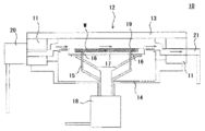
以下の実施例1~3、及び比較例1で用いたPoly-Si成長する枚葉式の気相成長装置(反応炉)を示す概略図を図4に示す。気相成長装置10のチャンバー(反応容器)12は、チャンバーベース11とチャンバーベース11を上下から挟む透明石英部材13、14とから形成される。このチャンバー12内には、シリコン単結晶基板Wを上面のウェーハ載置面(座ぐり部)19で支持するサセプタ17が配置されている。このサセプタ17には、例えば3つ以上の貫通孔16が設けられ、この貫通孔16に挿入されて上下動することでシリコン単結晶基板Wの載置、離間を行うウェーハリフトピン15が配置されている。このサセプタ17はウェーハ回転機構18に接続されており、エピタキシャル成長中はサセプタ17を回転させることで、載置されたシリコン単結晶基板Wを回転させ、Poly-Si層をシリコン単結晶基板W上に膜厚均一に成長させる。チャンバー12には、チャンバー12内に原料ガスおよびキャリアガス(例えば、水素)を含む気相成長ガスを導入して、サセプタ17上に載置されたシリコン単結晶基板Wの表面上に原料ガスとキャリアガスを供給するガス導入管20が接続されている。また、チャンバー12のガス導入管20が接続された側の反対側には、チャンバー12内からガスを排出するガス排出管21が接続されている。
Figure 4 shows a schematic diagram of a single-wafer vapor phase growth apparatus (reactor) for growing Poly-Si used in the following Examples 1 to 3 and Comparative Example 1. The chamber (reaction vessel) 12 of the vapor
(実施例1)
異なる2つの反応炉(RCT-A、RCT-B)にて以下の実験を実施した。不純物としてボロンを含有した抵抗率が5000Ω・cm以上、直径が200mmのシリコン単結晶基板を用意した。そのシリコン単結晶基板上に、成長温度870℃、成膜ガスにトリクロロシラン(TCS)を用いてPoly-Si膜厚0.3μm(1層目)となるようなノンドープのPoly-Si膜(第一のポリシリコン層)を成長させ、その後、成長温度1070℃に変更し、Poly-Si膜厚1.9μm(2層目)となるようなノンドープのPoly-Si膜(第二のポリシリコン層)を連続で成膜するCVD法を行うことによってサンプルとなるPoly-Siウェーハを製造した。
Example 1
The following experiment was carried out in two different reactors (RCT-A, RCT-B). A silicon single crystal substrate containing boron as an impurity, with a resistivity of 5000 Ω cm or more and a diameter of 200 mm was prepared. On the silicon single crystal substrate, a non-doped Poly-Si film (first polysilicon layer) was grown at a growth temperature of 870°C using trichlorosilane (TCS) as a deposition gas to a Poly-Si film thickness of 0.3 μm (first layer), and then the growth temperature was changed to 1070°C, and a non-doped Poly-Si film (second polysilicon layer) was continuously grown to a Poly-Si film thickness of 1.9 μm (second layer) by a CVD method, thereby manufacturing a sample Poly-Si wafer.
このときRCT-AおよびBの1層目の成膜工程で膜厚分布をいずれも1.5%に調整(予め定めた範囲の最大値(%)と最小値(%)の差を0(%)に制御)したうえで2層目の膜厚分布もRCT-A、Bどちらも1.5%となるように調整した。 In this case, the film thickness distribution in the deposition process of the first layer of RCT-A and B was adjusted to 1.5% (the difference between the maximum value (%) and the minimum value (%) of a predetermined range was controlled to 0 (%)), and the film thickness distribution of the second layer was also adjusted to 1.5% for both RCT-A and B.
このとき製造されたPoly-Siウェーハのウェーハ形状(Bow)を測定した。図1にそのときの結果を示す。図1より、RCT-A、Bで製造したウェーハのBowの値はいずれも4.35μm程度であり、RCT-A、Bの1層目の膜厚分布を同レベルにすることで同レベルのウェーハ形状を再現できることが確認できた。 The wafer shape (bow) of the Poly-Si wafers produced at this time was measured. The results are shown in Figure 1. As can be seen from Figure 1, the bow values of the wafers produced by RCT-A and B were both around 4.35 μm, and it was confirmed that the same level of wafer shape can be reproduced by making the film thickness distribution of the first layer of RCT-A and B the same level.
図1中における左図は、1層目の膜厚分布を確認するために、1層目を本来の0.3μmよりも厚く(2.5μm程度に)成膜して、ウェーハ面内の膜厚をプロットした図である。また、上記左図の横軸は膜厚測定位置を示しており、CTR:ウェーハ中心部、R/2:ウェーハ中心部から50mm、10mm:ウェーハ中心部から90mm(外周から10mm)である。図1中における右図は、設計膜厚(1層目0.3μm、2層目1.9μm)通りに成膜したときのウェーハのBowの値である。なお、1層目を本来の0.3μmに成膜した場合もより厚く成膜した場合も、面内膜厚分布(%)の計算値は理論上同じ値になる。 The left diagram in Figure 1 plots the film thickness within the wafer when the first layer is deposited thicker than the original 0.3 μm (approximately 2.5 μm) to confirm the film thickness distribution of the first layer. The horizontal axis in the left diagram indicates the film thickness measurement position, where CTR is the center of the wafer, R/2 is 50 mm from the center of the wafer, and 10 mm is 90 mm from the center of the wafer (10 mm from the outer periphery). The right diagram in Figure 1 shows the bow value of the wafer when the film is deposited according to the designed film thickness (first layer 0.3 μm, second layer 1.9 μm). Theoretically, the calculated value of the in-plane film thickness distribution (%) is the same whether the first layer is deposited to the original 0.3 μm or thicker.
(実施例2)
RCT-Aの1層目の成膜工程で膜厚分布を1.5%に調整し、RCT-Bの1層目の成膜工程で膜厚分布を6.7%に調整(予め定めた範囲の最大値(%)と最小値(%)の差を5.2(%)に制御)した以外は、実施例1と同様にしてPoly-Siウェーハを製造した。なお、2層目の膜厚分布も、実施例1と同様、RCT-A、Bどちらも1.5%となるように調整した。
Example 2
Poly-Si wafers were manufactured in the same manner as in Example 1, except that the film thickness distribution was adjusted to 1.5% in the film formation process of the first layer of RCT-A and the film thickness distribution was adjusted to 6.7% in the film formation process of the first layer of RCT-B (the difference between the maximum value (%) and the minimum value (%) of a predetermined range was controlled to 5.2 (%)). The film thickness distribution of the second layer was also adjusted to 1.5% for both RCT-A and B, as in Example 1.
実施例2で製造したPoly-Siウェーハのウェーハ形状(Bow)を測定したところ、RCT-A、Bで製造したウェーハのBowの値はいずれも4.35μm程度であり、RCT-AとRCT-Bで同レベルの形状(Bow)のウェーハが得られた。 When the wafer shape (bow) of the Poly-Si wafers produced in Example 2 was measured, the bow values of the wafers produced by RCT-A and RCT-B were both about 4.35 μm, meaning that RCT-A and RCT-B produced wafers with the same level of shape (bow).
(実施例3)
RCT-Aの1層目の成膜工程で膜厚分布を6.8%に調整し、RCT-Bの1層目の成膜工程で膜厚分布を6.8%に調整(予め定めた範囲の最大値(%)と最小値(%)の差を0(%)に制御)した以外は、実施例1と同様にしてPoly-Siウェーハを製造した。なお、2層目の膜厚分布も、実施例1と同様、RCT-A、Bどちらも1.5%となるように調整した。
Example 3
Poly-Si wafers were manufactured in the same manner as in Example 1, except that the film thickness distribution was adjusted to 6.8% in the film formation process of the first layer of RCT-A, and the film thickness distribution was adjusted to 6.8% in the film formation process of the first layer of RCT-B (the difference between the maximum value (%) and the minimum value (%) of a predetermined range was controlled to 0 (%)). The film thickness distribution of the second layer was also adjusted to 1.5% for both RCT-A and B, as in Example 1.
実施例3で製造したPoly-Siウェーハのウェーハ形状(Bow)を測定したところ、RCT-A、Bで製造したウェーハのBowの値はいずれも3.20μm程度であり、RCT-AとRCT-Bで同レベルの形状(Bow)のウェーハが得られた。 When the wafer shape (bow) of the Poly-Si wafers produced in Example 3 was measured, the bow values of the wafers produced by RCT-A and RCT-B were both approximately 3.20 μm, meaning that RCT-A and RCT-B produced wafers with the same level of shape (bow).
(比較例1)
RCT-Aの1層目の成膜工程で膜厚分布を1.5%、RCT-Bの1層目の成膜工程で膜厚分布を6.8%に調整(予め定めた範囲の最大値(%)と最小値(%)の差を5.3(%)に制御)した以外は、実施例1と同様にしてPoly-Siウェーハを製造した。なお、実施例1と同様、2層目の膜厚分布もRCT-A、Bどちらも1.5%となるように調整した。
(Comparative Example 1)
Poly-Si wafers were manufactured in the same manner as in Example 1, except that the film thickness distribution was adjusted to 1.5% in the film formation process of the first layer of RCT-A and 6.8% in the film formation process of the first layer of RCT-B (the difference between the maximum value (%) and the minimum value (%) of a predetermined range was controlled to 5.3 (%)). Note that, like in Example 1, the film thickness distribution of the second layer was also adjusted to 1.5% for both RCT-A and B.
このとき製造されたPoly-Siウェーハのウェーハ形状(Bow)を測定した。図1にそのときの結果を示す。図1より、RCT-Aで製造したウェーハのBowは4.35μm程度であったのに対し、RCT-Bで製造したウェーハのBowは3.20μm程度であり、第一のポリシリコン層の面内膜厚分布を最大値(%)と最小値(%)の差が5.2(%)以内となる範囲に制御しなかったことで、異なるウェーハ形状となることが確認できた。 The wafer shape (bow) of the Poly-Si wafers produced at this time was measured. Figure 1 shows the results. As can be seen from Figure 1, the bow of the wafer produced by RCT-A was approximately 4.35 μm, while the bow of the wafer produced by RCT-B was approximately 3.20 μm. It was confirmed that the wafer shapes were different because the in-plane film thickness distribution of the first polysilicon layer was not controlled to a range where the difference between the maximum value (%) and the minimum value (%) was within 5.2 (%).
本明細書は、以下の発明を包含する。
[1]:シリコン単結晶基板上にポリシリコン層が成膜されたポリシリコンウェーハの製
造方法であって、(1)シリコン単結晶基板上に、CVD法により1000℃以
下の温度で第一のポリシリコン層を成膜する工程、(2)前記第一のポリシリコ
ン層上に、CVD法により1000℃より高い温度で第二のポリシリコン層を成
膜する工程、を有し、かつ、前記工程(1)において、成膜する前記第一のポリ
シリコン層の面内膜厚分布の値(%)を、予め定めた範囲内に制御するようにし
、かつ、前記予め定めた範囲の最大値(%)と最小値(%)の差を5.2(%)
以内とすることを特徴とするポリシリコンウェーハの製造方法。
[2]:前記工程(1)において、前記予め定めた範囲の最大値(%)を、1.5%以下
に制御することを特徴とする請求項1に記載のポリシリコンウェーハの製造方法
。
[3]:前記工程(1)において、前記シリコン単結晶基板の面内温度分布を制御するこ
とによって、成膜する前記第一のポリシリコン層の面内膜厚分布を制御すること
を特徴とする上記[1]に記載のポリシリコンウェーハの製造方法。
[4]:前記工程(1)において、前記シリコン単結晶基板の面内温度分布を制御するこ
とによって、成膜する前記第一のポリシリコン層の面内膜厚分布を制御すること
を特徴とする上記[2]に記載のポリシリコンウェーハの製造方法。
[5]:2以上の異なる製造設備を用いてポリシリコンウェーハを製造するためのポリシ
リコンウェーハの製造方法であって、前記2以上の異なる製造設備の各々におい
て、上記[1]、上記[2]、上記[3]、又は上記[4]に記載のポリシリコ
ンウェーハの製造方法を用いてポリシリコンウェーハを製造することを特徴とす
るポリシリコンウェーハの製造方法。
This specification includes the following inventions.
[1]: A method for manufacturing a polysilicon wafer in which a polysilicon layer is formed on a silicon single crystal substrate, comprising: (1) a step of forming a first polysilicon layer on a silicon single crystal substrate at a temperature of 1000° C. or less by a CVD method; and (2) a step of forming a second polysilicon layer on the first polysilicon layer at a temperature higher than 1000° C. by a CVD method, wherein in the step (1), a value (%) of an in-plane film thickness distribution of the first polysilicon layer to be formed is controlled within a predetermined range, and the difference between a maximum value (%) and a minimum value (%) of the predetermined range is controlled to be 5.2 (%).
4. A method for producing a polysilicon wafer, comprising the steps of:
[2]: The method for producing a polysilicon wafer according to
[3]: The method for producing a polysilicon wafer according to the above [1], characterized in that in the step (1), an in-plane temperature distribution of the silicon single crystal substrate is controlled to thereby control an in-plane film thickness distribution of the first polysilicon layer to be formed.
[4]: The method for producing a polysilicon wafer according to the above [2], characterized in that in the step (1), an in-plane temperature distribution of the silicon single crystal substrate is controlled to thereby control an in-plane film thickness distribution of the first polysilicon layer to be formed.
[5]: A method for producing a polysilicon wafer using two or more different manufacturing facilities, characterized in that in each of the two or more different manufacturing facilities, a polysilicon wafer is produced using the method for producing a polysilicon wafer described in [1], [2], [3], or [4] above.
なお、本発明は、上記実施形態に限定されるものではない。上記実施形態は例示であり、本発明の特許請求の範囲に記載された技術的思想と実質的に同一な構成を有し、同様な作用効果を奏するものは、いかなるものであっても本発明の技術的範囲に包含される。 The present invention is not limited to the above-described embodiment. The above-described embodiment is merely an example, and anything that has substantially the same configuration as the technical idea described in the claims of the present invention and exhibits similar effects is included within the technical scope of the present invention.
1…シリコン単結晶基板、 2…第一のポリシリコン層、
3…第二のポリシリコン層、 4…ポリシリコンウェーハ、 10…気相成長装置、
11…チャンバーベース、 12…チャンバー、 13、14…透明石英部材、
15…ウェーハリフトピン、 16…貫通孔、 17…サセプタ、
18…ウェーハ回転機構、 19…ウェーハ載置面、 20…ガス導入管、
21…ガス排出管。 W…シリコン単結晶基板。
1...silicon single crystal substrate; 2...first polysilicon layer;
3... second polysilicon layer, 4... polysilicon wafer, 10... vapor phase growth apparatus,
11 ... chamber base; 12 ... chamber; 13, 14 ... transparent quartz members;
15: wafer lift pin; 16: through hole; 17: susceptor;
18...wafer rotation mechanism; 19...wafer placement surface; 20...gas introduction pipe;
21: Gas exhaust pipe. W: Silicon single crystal substrate.
Claims (5)
(1)シリコン単結晶基板上に、CVD法により1000℃以下の温度で第一のポリシリコン層を成膜する工程、
(2)前記第一のポリシリコン層上に、CVD法により1000℃より高い温度で第二のポリシリコン層を成膜する工程、
を有し、かつ、
前記工程(1)において、成膜する前記第一のポリシリコン層の面内膜厚分布の値(%)を、予め定めた範囲内に制御するようにし、かつ、前記予め定めた範囲の最大値(%)と最小値(%)の差を5.2(%)以内とすることを特徴とするポリシリコンウェーハの製造方法。 A method for manufacturing a polysilicon wafer in which a polysilicon layer is formed on a silicon single crystal substrate, comprising the steps of:
(1) forming a first polysilicon layer on a silicon single crystal substrate by a CVD method at a temperature of 1000° C. or less;
(2) forming a second polysilicon layer on the first polysilicon layer by a CVD method at a temperature higher than 1000° C.;
and
In the step (1), a value (%) of an in-plane film thickness distribution of the first polysilicon layer to be formed is controlled within a predetermined range, and a difference between a maximum value (%) and a minimum value (%) of the predetermined range is set to within 5.2 (%).
前記2以上の異なる製造設備の各々において、請求項1から請求項4のいずれか一項に記載のポリシリコンウェーハの製造方法を用いてポリシリコンウェーハを製造することを特徴とするポリシリコンウェーハの製造方法。 A method for producing a polysilicon wafer using two or more different manufacturing facilities, comprising:
A method for producing a polysilicon wafer, comprising the steps of: producing a polysilicon wafer by using the method for producing a polysilicon wafer according to any one of claims 1 to 4 in each of the two or more different production facilities.
Priority Applications (4)
| Application Number | Priority Date | Filing Date | Title |
|---|---|---|---|
| JP2022067299A JP7697397B2 (en) | 2022-04-15 | 2022-04-15 | Polysilicon wafer manufacturing method |
| PCT/JP2023/008830 WO2023199656A1 (en) | 2022-04-15 | 2023-03-08 | Method for producing polysilicon wafer |
| CN202380033330.8A CN118922913A (en) | 2022-04-15 | 2023-03-08 | Method for manufacturing polycrystalline silicon wafer |
| KR1020247033803A KR20250005115A (en) | 2022-04-15 | 2023-03-08 | Method for manufacturing polysilicon wafers |
Applications Claiming Priority (1)
| Application Number | Priority Date | Filing Date | Title |
|---|---|---|---|
| JP2022067299A JP7697397B2 (en) | 2022-04-15 | 2022-04-15 | Polysilicon wafer manufacturing method |
Publications (2)
| Publication Number | Publication Date |
|---|---|
| JP2023157404A JP2023157404A (en) | 2023-10-26 |
| JP7697397B2 true JP7697397B2 (en) | 2025-06-24 |
Family
ID=88329283
Family Applications (1)
| Application Number | Title | Priority Date | Filing Date |
|---|---|---|---|
| JP2022067299A Active JP7697397B2 (en) | 2022-04-15 | 2022-04-15 | Polysilicon wafer manufacturing method |
Country Status (4)
| Country | Link |
|---|---|
| JP (1) | JP7697397B2 (en) |
| KR (1) | KR20250005115A (en) |
| CN (1) | CN118922913A (en) |
| WO (1) | WO2023199656A1 (en) |
Citations (4)
| Publication number | Priority date | Publication date | Assignee | Title |
|---|---|---|---|---|
| JP2000183153A (en) | 1998-12-17 | 2000-06-30 | Mitsubishi Materials Silicon Corp | Dielectric isolation wafer and manufacture thereof |
| JP2004158685A (en) | 2002-11-07 | 2004-06-03 | Canon Inc | Polycrystalline silicon thin film and its manufacturing method |
| JP2014011178A (en) | 2012-06-27 | 2014-01-20 | Tokyo Electron Ltd | Plasma processing method and plasma processing apparatus |
| WO2017221563A1 (en) | 2016-06-23 | 2017-12-28 | 信越半導体株式会社 | Bonded soi wafer manufacturing method |
Family Cites Families (3)
| Publication number | Priority date | Publication date | Assignee | Title |
|---|---|---|---|---|
| JPS57197834A (en) * | 1981-05-29 | 1982-12-04 | Toko Inc | Manufacture of insulated and isolated substrate |
| JPH1116991A (en) | 1997-06-19 | 1999-01-22 | Tokai Carbon Co Ltd | Carbon support for semiconductor manufacturing equipment |
| JP5343409B2 (en) | 2008-06-06 | 2013-11-13 | 株式会社Sumco | Method for determining curvature of semiconductor wafer, method for manufacturing wafer with film |
-
2022
- 2022-04-15 JP JP2022067299A patent/JP7697397B2/en active Active
-
2023
- 2023-03-08 WO PCT/JP2023/008830 patent/WO2023199656A1/en not_active Ceased
- 2023-03-08 KR KR1020247033803A patent/KR20250005115A/en active Pending
- 2023-03-08 CN CN202380033330.8A patent/CN118922913A/en active Pending
Patent Citations (4)
| Publication number | Priority date | Publication date | Assignee | Title |
|---|---|---|---|---|
| JP2000183153A (en) | 1998-12-17 | 2000-06-30 | Mitsubishi Materials Silicon Corp | Dielectric isolation wafer and manufacture thereof |
| JP2004158685A (en) | 2002-11-07 | 2004-06-03 | Canon Inc | Polycrystalline silicon thin film and its manufacturing method |
| JP2014011178A (en) | 2012-06-27 | 2014-01-20 | Tokyo Electron Ltd | Plasma processing method and plasma processing apparatus |
| WO2017221563A1 (en) | 2016-06-23 | 2017-12-28 | 信越半導体株式会社 | Bonded soi wafer manufacturing method |
Also Published As
| Publication number | Publication date |
|---|---|
| JP2023157404A (en) | 2023-10-26 |
| KR20250005115A (en) | 2025-01-09 |
| WO2023199656A1 (en) | 2023-10-19 |
| CN118922913A (en) | 2024-11-08 |
Similar Documents
| Publication | Publication Date | Title |
|---|---|---|
| JP4417625B2 (en) | Method of forming film on mixed substrate using trisilane and method of manufacturing base structure | |
| EP3260581B1 (en) | Method for producing silicon carbide single crystal epitaxial wafer and silicon carbide single crystal epitaxial wafer | |
| CN104718601A (en) | SiC substrate with SiC epitaxial film | |
| JP5910430B2 (en) | Method for manufacturing epitaxial silicon carbide wafer | |
| US8038793B2 (en) | Epitaxial growth method | |
| JP7694744B2 (en) | SiC device and method for manufacturing SiC device | |
| JP7816191B2 (en) | SiC epitaxial wafer and SiC device | |
| CN115537922B (en) | Method for reducing self-doping of epitaxial wafer | |
| JP2009038294A (en) | Output adjustment method, silicon epitaxial wafer manufacturing method, and susceptor | |
| JP7697397B2 (en) | Polysilicon wafer manufacturing method | |
| JP2008186944A (en) | Vapor growth susceptor, vapor growth apparatus, vapor growth susceptor design method and vapor growth method | |
| JP5780491B2 (en) | Manufacturing method of silicon epitaxial wafer | |
| JPH10189695A (en) | Vapor growth susceptor and manufacture thereof | |
| US20240191393A1 (en) | Epitaxy susceptor, epitaxy growth apparatus and manufacturing method of semiconductor device | |
| JP3424069B2 (en) | Manufacturing method of epitaxial silicon substrate | |
| WO2020158657A1 (en) | Film forming apparatus and film forming method | |
| JP2021031363A (en) | Method for manufacturing silicon carbide polycrystal substrate | |
| JP7392526B2 (en) | Method for manufacturing silicon carbide single crystal substrate | |
| JP7255473B2 (en) | Method for manufacturing polycrystalline silicon carbide substrate | |
| JP7567210B2 (en) | Method for manufacturing silicon carbide single crystal substrate | |
| KR20110087440A (en) | Susceptor for semiconductor manufacturing and semiconductor manufacturing apparatus including same | |
| JPH08250430A (en) | Manufacture of single-crystal thin film | |
| JP3112796B2 (en) | Chemical vapor deposition method | |
| CN120767187A (en) | Epitaxial wafer and method and device for improving flatness of epitaxial wafer | |
| KR101905860B1 (en) | Method of fabrication wafer |
Legal Events
| Date | Code | Title | Description |
|---|---|---|---|
| A621 | Written request for application examination |
Free format text: JAPANESE INTERMEDIATE CODE: A621 Effective date: 20240327 |
|
| TRDD | Decision of grant or rejection written | ||
| A01 | Written decision to grant a patent or to grant a registration (utility model) |
Free format text: JAPANESE INTERMEDIATE CODE: A01 Effective date: 20250513 |
|
| A61 | First payment of annual fees (during grant procedure) |
Free format text: JAPANESE INTERMEDIATE CODE: A61 Effective date: 20250526 |
|
| R150 | Certificate of patent or registration of utility model |
Ref document number: 7697397 Country of ref document: JP Free format text: JAPANESE INTERMEDIATE CODE: R150 |