JP7689428B2 - 半導体装置 - Google Patents
半導体装置 Download PDFInfo
- Publication number
- JP7689428B2 JP7689428B2 JP2021009959A JP2021009959A JP7689428B2 JP 7689428 B2 JP7689428 B2 JP 7689428B2 JP 2021009959 A JP2021009959 A JP 2021009959A JP 2021009959 A JP2021009959 A JP 2021009959A JP 7689428 B2 JP7689428 B2 JP 7689428B2
- Authority
- JP
- Japan
- Prior art keywords
- region
- gate electrode
- semiconductor device
- drain region
- transistor
- Prior art date
- Legal status (The legal status is an assumption and is not a legal conclusion. Google has not performed a legal analysis and makes no representation as to the accuracy of the status listed.)
- Active
Links
Images


Classifications
-
- H—ELECTRICITY
- H10—SEMICONDUCTOR DEVICES; ELECTRIC SOLID-STATE DEVICES NOT OTHERWISE PROVIDED FOR
- H10D—INORGANIC ELECTRIC SEMICONDUCTOR DEVICES
- H10D64/00—Electrodes of devices having potential barriers
- H10D64/20—Electrodes characterised by their shapes, relative sizes or dispositions
- H10D64/27—Electrodes not carrying the current to be rectified, amplified, oscillated or switched, e.g. gates
- H10D64/311—Gate electrodes for field-effect devices
- H10D64/411—Gate electrodes for field-effect devices for FETs
- H10D64/511—Gate electrodes for field-effect devices for FETs for IGFETs
- H10D64/517—Gate electrodes for field-effect devices for FETs for IGFETs characterised by the conducting layers
- H10D64/519—Gate electrodes for field-effect devices for FETs for IGFETs characterised by the conducting layers characterised by their top-view geometrical layouts
-
- H—ELECTRICITY
- H10—SEMICONDUCTOR DEVICES; ELECTRIC SOLID-STATE DEVICES NOT OTHERWISE PROVIDED FOR
- H10D—INORGANIC ELECTRIC SEMICONDUCTOR DEVICES
- H10D89/00—Aspects of integrated devices not covered by groups H10D84/00 - H10D88/00
- H10D89/60—Integrated devices comprising arrangements for electrical or thermal protection, e.g. protection circuits against electrostatic discharge [ESD]
- H10D89/601—Integrated devices comprising arrangements for electrical or thermal protection, e.g. protection circuits against electrostatic discharge [ESD] for devices having insulated gate electrodes, e.g. for IGFETs or IGBTs
- H10D89/811—Integrated devices comprising arrangements for electrical or thermal protection, e.g. protection circuits against electrostatic discharge [ESD] for devices having insulated gate electrodes, e.g. for IGFETs or IGBTs using FETs as protective elements
-
- H—ELECTRICITY
- H10—SEMICONDUCTOR DEVICES; ELECTRIC SOLID-STATE DEVICES NOT OTHERWISE PROVIDED FOR
- H10D—INORGANIC ELECTRIC SEMICONDUCTOR DEVICES
- H10D30/00—Field-effect transistors [FET]
- H10D30/60—Insulated-gate field-effect transistors [IGFET]
-
- H—ELECTRICITY
- H10—SEMICONDUCTOR DEVICES; ELECTRIC SOLID-STATE DEVICES NOT OTHERWISE PROVIDED FOR
- H10D—INORGANIC ELECTRIC SEMICONDUCTOR DEVICES
- H10D64/00—Electrodes of devices having potential barriers
- H10D64/111—Field plates
-
- H—ELECTRICITY
- H10—SEMICONDUCTOR DEVICES; ELECTRIC SOLID-STATE DEVICES NOT OTHERWISE PROVIDED FOR
- H10D—INORGANIC ELECTRIC SEMICONDUCTOR DEVICES
- H10D64/00—Electrodes of devices having potential barriers
- H10D64/20—Electrodes characterised by their shapes, relative sizes or dispositions
- H10D64/23—Electrodes carrying the current to be rectified, amplified, oscillated or switched, e.g. sources, drains, anodes or cathodes
- H10D64/251—Source or drain electrodes for field-effect devices
- H10D64/258—Source or drain electrodes for field-effect devices characterised by the relative positions of the source or drain electrodes with respect to the gate electrode
-
- H—ELECTRICITY
- H10—SEMICONDUCTOR DEVICES; ELECTRIC SOLID-STATE DEVICES NOT OTHERWISE PROVIDED FOR
- H10D—INORGANIC ELECTRIC SEMICONDUCTOR DEVICES
- H10D64/00—Electrodes of devices having potential barriers
- H10D64/20—Electrodes characterised by their shapes, relative sizes or dispositions
- H10D64/27—Electrodes not carrying the current to be rectified, amplified, oscillated or switched, e.g. gates
- H10D64/311—Gate electrodes for field-effect devices
- H10D64/411—Gate electrodes for field-effect devices for FETs
- H10D64/511—Gate electrodes for field-effect devices for FETs for IGFETs
- H10D64/517—Gate electrodes for field-effect devices for FETs for IGFETs characterised by the conducting layers
- H10D64/518—Gate electrodes for field-effect devices for FETs for IGFETs characterised by the conducting layers characterised by their lengths or sectional shapes
-
- H—ELECTRICITY
- H10—SEMICONDUCTOR DEVICES; ELECTRIC SOLID-STATE DEVICES NOT OTHERWISE PROVIDED FOR
- H10D—INORGANIC ELECTRIC SEMICONDUCTOR DEVICES
- H10D64/00—Electrodes of devices having potential barriers
- H10D64/20—Electrodes characterised by their shapes, relative sizes or dispositions
- H10D64/27—Electrodes not carrying the current to be rectified, amplified, oscillated or switched, e.g. gates
- H10D64/311—Gate electrodes for field-effect devices
Landscapes
- Semiconductor Integrated Circuits (AREA)
- Metal-Oxide And Bipolar Metal-Oxide Semiconductor Integrated Circuits (AREA)
- Insulated Gate Type Field-Effect Transistor (AREA)
Description
一方、CDMは、近年の製造工程の自動化により人間が半導体装置に触れる作業が減っていることからHBMよりも注目されている。このCDMは、帯電した半導体装置の端子から装置や治工具類などの金属部に接触して放電するモデルであり、比較的小さいエネルギー量ではあるが数10psec~数100psecという極めて短い時間で半導体装置から放電する。
MOSトランジスタのゲート電極及びソース領域が第1の電源端子又は第2の電源端子に接続され、ドレイン領域が外部信号端子に接続されているオフトランジスタを有する半導体装置において、
前記オフトランジスタは、ゲート電極がチャネル領域に加えてドレイン領域の一部又は全部の上方に延設され、前記ドレイン領域と前記ドレイン領域の上方に延設されている前記ゲート電極との間に容量形成領域を備える。
図1は、第1の実施形態に係る半導体装置が有するオフトランジスタを示す回路図である。
図1に示すように、半導体装置100は、電源電位である第1の電源端子100aと、半導体装置100をオンオフする制御信号が入力される外部信号端子100bと、接地電位である第2の電源端子100cと、オフトランジスタ10と、を有する。
なお、本実施形態では、外部信号端子100bに半導体装置100をオンオフする制御信号が入力されるとしたが、これに限ることなく、他の信号でもよい。
なお、半導体装置としては、特に制限はなく、目的に応じて適宜選択することができ、例えば、レギュレータ、センサ、メモリ、バッテリ制御等の機能を有する半導体装置などが挙げられる。
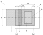
なお、アクティブ領域Aは、素子分離領域Bで他の素子から電気的に分離されている。
なお、素子分離領域Bは、本実施形態のように分離用酸化膜2としてLOCOS膜を用いたもので形成してもよく、トレンチ分離(Shallow Trench Isolation:STI)により形成してもよい。
ドレイン領域5及びソース領域6のN型の不純物は、イオン注入法などによりシリコン半導体基板面の略法線方向からゲート電極3の周囲に注入され、続く半導体装置の製造工程における熱処理によってゲート電極3の下面にも拡散する。このため、シリコン半導体基板をその法線方向から平面視した際に、ドレイン領域5及びソース領域6には、ゲート電極3の外周部の直下に位置する部分が存在する。
これにより、ゲート電極3の直下には、ゲート絶縁膜4を介して、ウェル領域1、ドレイン領域5及びソース領域6が存在することから、それぞれ容量が形成される。
また、素子分離領域B下に形成されているチャネルストッパーの役目を果たすウェル領域1よりもP型の不純物濃度の高い領域とドレイン領域5との接触を避けるように故意に離間させて高耐圧構造としてもよい。これにより、ゲート電極3とドレイン領域5との間の容量形成領域Ca2を大きく増大させることが可能となる。
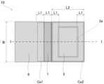
図5は、第2の実施形態に係る半導体装置が有するオフトランジスタを示す概略平面図である。図6は、図5のII-II線における概略断面図である。
図5及び図6に示すように、第2の実施形態は、第1の実施形態において開口部3aを平面視した際の形状を矩形状から櫛状とした開口部8aに変更した以外は、第1の実施形態と同様である。したがって、図2~図4で説明した第1の実施形態と同じ構成については、同じ符号を記すことで説明に代える。
また、開口部8aが櫛状であると、ドレイン領域5及びソース領域6を形成する際に、ウェル領域1の表面に不純物を注入しやすくなる点で有利である。
2 分離用酸化膜
3,8 ゲート電極
3a,8a 開口部
4 ゲート絶縁膜
5 ドレイン領域
6 ソース領域
10 オフトランジスタ
100 半導体装置
100a 第1の電源端子
100b 外部信号端子
100c 第2の電源端子
A アクティブ領域
B 素子分離領域
Ca1 (ゲート電極とウェル領域及びソース領域との間の)容量形成領域
Ca2 (ゲート電極とドレイン領域との間の)容量形成領域
Claims (5)
- MOSトランジスタのゲート電極及びソース領域が接地され、ドレイン領域が外部信号端子に接続されているオフトランジスタを有する半導体装置において、
前記オフトランジスタは、前記ドレイン領域及び前記ソース領域が接地電位のウェル領域に形成されており、前記ゲート電極がチャネル領域に加えて前記ドレイン領域の上方に延設され、
前記ゲート電極と前記ドレイン領域との間で形成される容量は、前記ゲート電極と前記ウェル領域及び前記ソース領域との間に生じる容量よりも大きいことを特徴とする半導体装置。 - 前記ゲート電極は、前記ドレイン領域を覆う箇所に開口部が設けられている請求項1に記載の半導体装置。
- 前記開口部を平面視した際の形状は、矩形状である請求項2に記載の半導体装置。
- 前記開口部を平面視した際の形状は、矩形状の一部に凹部を有する請求項3に記載の半導体装置。
- 前記開口部を平面視した際の形状が櫛状である請求項2に記載の半導体装置。
Priority Applications (3)
| Application Number | Priority Date | Filing Date | Title |
|---|---|---|---|
| JP2021009959A JP7689428B2 (ja) | 2021-01-26 | 2021-01-26 | 半導体装置 |
| US17/572,653 US11894364B2 (en) | 2021-01-26 | 2022-01-11 | Semiconductor device |
| CN202210036402.1A CN114792725A (zh) | 2021-01-26 | 2022-01-13 | 半导体装置 |
Applications Claiming Priority (1)
| Application Number | Priority Date | Filing Date | Title |
|---|---|---|---|
| JP2021009959A JP7689428B2 (ja) | 2021-01-26 | 2021-01-26 | 半導体装置 |
Publications (2)
| Publication Number | Publication Date |
|---|---|
| JP2022113931A JP2022113931A (ja) | 2022-08-05 |
| JP7689428B2 true JP7689428B2 (ja) | 2025-06-06 |
Family
ID=82459618
Family Applications (1)
| Application Number | Title | Priority Date | Filing Date |
|---|---|---|---|
| JP2021009959A Active JP7689428B2 (ja) | 2021-01-26 | 2021-01-26 | 半導体装置 |
Country Status (3)
| Country | Link |
|---|---|
| US (1) | US11894364B2 (ja) |
| JP (1) | JP7689428B2 (ja) |
| CN (1) | CN114792725A (ja) |
Families Citing this family (1)
| Publication number | Priority date | Publication date | Assignee | Title |
|---|---|---|---|---|
| CN119584645B (zh) * | 2025-02-05 | 2025-06-06 | 合肥晶合集成电路股份有限公司 | 半导体器件版图结构 |
Citations (1)
| Publication number | Priority date | Publication date | Assignee | Title |
|---|---|---|---|---|
| JP2011192843A (ja) | 2010-03-15 | 2011-09-29 | Seiko Instruments Inc | 半導体装置 |
Family Cites Families (8)
| Publication number | Priority date | Publication date | Assignee | Title |
|---|---|---|---|---|
| US5028819A (en) * | 1990-06-08 | 1991-07-02 | Zilog, Inc. | High CMOS open-drain output buffer |
| JPH07321306A (ja) * | 1994-03-31 | 1995-12-08 | Seiko Instr Inc | 半導体装置およびその製造方法 |
| JP3080028B2 (ja) * | 1997-02-28 | 2000-08-21 | 日本電気株式会社 | 半導体装置 |
| JP5656658B2 (ja) | 2011-01-14 | 2015-01-21 | セミコンダクター・コンポーネンツ・インダストリーズ・リミテッド・ライアビリティ・カンパニー | 半導体装置 |
| US9441656B2 (en) * | 2014-10-22 | 2016-09-13 | Vibration & Seismic Technologies, LLC | Strut and clip assembly for stiffening a hanger rod |
| CN105870117B (zh) | 2015-02-05 | 2020-09-25 | 艾普凌科有限公司 | 半导体装置 |
| JP6624912B2 (ja) | 2015-02-05 | 2019-12-25 | エイブリック株式会社 | 半導体装置 |
| US11579645B2 (en) * | 2019-06-21 | 2023-02-14 | Wolfspeed, Inc. | Device design for short-circuitry protection circuitry within transistors |
-
2021
- 2021-01-26 JP JP2021009959A patent/JP7689428B2/ja active Active
-
2022
- 2022-01-11 US US17/572,653 patent/US11894364B2/en active Active
- 2022-01-13 CN CN202210036402.1A patent/CN114792725A/zh active Pending
Patent Citations (1)
| Publication number | Priority date | Publication date | Assignee | Title |
|---|---|---|---|---|
| JP2011192843A (ja) | 2010-03-15 | 2011-09-29 | Seiko Instruments Inc | 半導体装置 |
Also Published As
| Publication number | Publication date |
|---|---|
| CN114792725A (zh) | 2022-07-26 |
| JP2022113931A (ja) | 2022-08-05 |
| US20220238510A1 (en) | 2022-07-28 |
| US11894364B2 (en) | 2024-02-06 |
Similar Documents
| Publication | Publication Date | Title |
|---|---|---|
| KR102361141B1 (ko) | 정전기 방전 보호용 반도체 소자 | |
| JPH0151070B2 (ja) | ||
| EP0703621B1 (en) | Electrostatic discharge protection device for MOS integrated circuits | |
| EP1515371B1 (en) | Semiconductor device comprising a MOS transistor and method of making the same | |
| US11239229B2 (en) | Self-biased bidirectional ESD protection circuit | |
| US20150129977A1 (en) | Semiconductor electrostatic discharge protection apparatus | |
| US7709896B2 (en) | ESD protection device and method | |
| EP0415255B1 (en) | Protection circuit for use in semiconductor integrated circuit device | |
| CN106960841A (zh) | 高压晶体管 | |
| EP0253105A1 (en) | Integrated circuit with improved protective device | |
| CN1319171C (zh) | 具有改进的静电放电耐压的半导体装置 | |
| JP7689428B2 (ja) | 半導体装置 | |
| CN110071106B (zh) | 半导体装置 | |
| CN103943612A (zh) | 静电放电保护装置 | |
| US6664599B1 (en) | ESD protection device | |
| JP2006080528A (ja) | 高電圧素子の静電気保護装置 | |
| JP7713874B2 (ja) | 半導体装置 | |
| JP4795613B2 (ja) | 半導体装置 | |
| US5521413A (en) | Semiconductor device having a solid metal wiring with a contact portion for improved protection | |
| JP2009038099A (ja) | 半導体装置 | |
| CN110690210B (zh) | 栅极接地n型金属氧化物半导体晶体管 | |
| US10741542B2 (en) | Transistors patterned with electrostatic discharge protection and methods of fabrication | |
| US7075156B1 (en) | Collector structure for electrostatic discharge protection circuits | |
| JP7671172B2 (ja) | 半導体装置 | |
| US6987301B1 (en) | Electrostatic discharge protection |
Legal Events
| Date | Code | Title | Description |
|---|---|---|---|
| A621 | Written request for application examination |
Free format text: JAPANESE INTERMEDIATE CODE: A621 Effective date: 20231205 |
|
| A131 | Notification of reasons for refusal |
Free format text: JAPANESE INTERMEDIATE CODE: A131 Effective date: 20250107 |
|
| A521 | Request for written amendment filed |
Free format text: JAPANESE INTERMEDIATE CODE: A523 Effective date: 20250128 |
|
| A131 | Notification of reasons for refusal |
Free format text: JAPANESE INTERMEDIATE CODE: A131 Effective date: 20250311 |
|
| A521 | Request for written amendment filed |
Free format text: JAPANESE INTERMEDIATE CODE: A523 Effective date: 20250507 |
|
| TRDD | Decision of grant or rejection written | ||
| A01 | Written decision to grant a patent or to grant a registration (utility model) |
Free format text: JAPANESE INTERMEDIATE CODE: A01 Effective date: 20250520 |
|
| A61 | First payment of annual fees (during grant procedure) |
Free format text: JAPANESE INTERMEDIATE CODE: A61 Effective date: 20250527 |
|
| R150 | Certificate of patent or registration of utility model |
Ref document number: 7689428 Country of ref document: JP Free format text: JAPANESE INTERMEDIATE CODE: R150 |