EP0253105A1 - Integrated circuit with improved protective device - Google Patents
Integrated circuit with improved protective device Download PDFInfo
- Publication number
- EP0253105A1 EP0253105A1 EP87107503A EP87107503A EP0253105A1 EP 0253105 A1 EP0253105 A1 EP 0253105A1 EP 87107503 A EP87107503 A EP 87107503A EP 87107503 A EP87107503 A EP 87107503A EP 0253105 A1 EP0253105 A1 EP 0253105A1
- Authority
- EP
- European Patent Office
- Prior art keywords
- region
- insulating layer
- layer
- protective device
- rectangular
- Prior art date
- Legal status (The legal status is an assumption and is not a legal conclusion. Google has not performed a legal analysis and makes no representation as to the accuracy of the status listed.)
- Granted
Links
Images

Classifications
-
- H—ELECTRICITY
- H01—ELECTRIC ELEMENTS
- H01L—SEMICONDUCTOR DEVICES NOT COVERED BY CLASS H10
- H01L27/00—Devices consisting of a plurality of semiconductor or other solid-state components formed in or on a common substrate
- H01L27/02—Devices consisting of a plurality of semiconductor or other solid-state components formed in or on a common substrate including semiconductor components specially adapted for rectifying, oscillating, amplifying or switching and having at least one potential-jump barrier or surface barrier; including integrated passive circuit elements with at least one potential-jump barrier or surface barrier
- H01L27/0203—Particular design considerations for integrated circuits
- H01L27/0248—Particular design considerations for integrated circuits for electrical or thermal protection, e.g. electrostatic discharge [ESD] protection
- H01L27/0251—Particular design considerations for integrated circuits for electrical or thermal protection, e.g. electrostatic discharge [ESD] protection for MOS devices
- H01L27/0266—Particular design considerations for integrated circuits for electrical or thermal protection, e.g. electrostatic discharge [ESD] protection for MOS devices using field effect transistors as protective elements
Abstract
Description
- The present invention relates to a semiconductor integrated circuit fabricated on a semiconductor substrate, and more particularly to a protective device for preventing an integrated circuit fabricated on the same substrate from destruction due to excessive electrostatic charges.
- In order to prevent an active element such as a MOS field effect transistor and a bipolar transistor from destruction due to excessive electrostatic charge applied to an external terminal which is connected to the active element, a protective device is connected with the external terminal.
- A typical example of a known protective device is composed of a resistor connected in series between the external terminal and an electrode of the active element such as a gate of MOS transistor and a protecting MOS transistor connected between the electrode of the active element and a ground potential source with a gate connected to the ground potontial source. The external terminal is formed by a bonding pad having a relatively large area and the resistor is formed by a diffusion region extending from the bonding pad to a drain of the protecting MOS transistor.
- The diffusion region as the resistor is required to be formed with a relatively large length to obtain a predetermined resistance value. Accordingly, a relatively large area is required to fabricate the protecting device on a semiconductor substrate. Furthermore, if another diffusion region is formed adjacent to the diffusion region (resistor diffusion region) serving as the resistor, a parasitic bipolar transistor is produced therebetween, and when an excessive voltage is applied to the bonding pad and the resistor diffusion, an abnormal current flows between the resistor diffusion region and the above additional diffusion region. Therefore, a certain distance must be kept between the resistor diffusion region and the another diffusion region to avoid the above parasitic transistor. Thus, the further area on the semiconductor substrate have been required to arrange the protective device and a predetermined function circuit on the same substrate.
- It is one object of the present invention to provide a semiconductor integrated circuit with an improved protective device.
- It is another object of the present invention to provide a high-density semiconductor integrated circuit having a reduced-sized protective device.
- The protective device for a functional circuit according to the present invention comprises a punch- through type protective transistor connected between an input electrode or pad and a reference voltage terminal and a resistor connected between the input electrode and the functional circuit.
- The punch-through type protective transistor is made of first and second spaced-apart impurity regions formed in a semiconductor substrate. The first region is electrically connected to the input pad and the second impurity region is electrically connected to the reference voltage terminal.
- The resistor is made of a strip-shaped impurity region having one end connected to the opposite side of the first impurity region not facing the second region and extends therefrom under the input pad towards the functional circuit. The input pad thus overlaps a part of the strip-shaped resistor region.
-
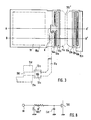
- Fig. 1 is a schematic circuit diagram of a protective device according to a prior art;
- Fig. 2 is a plan view of a protective device according to a prior art;
- Fig. 3 is a plan view showing a protective device and a MOS transistor to be protected;
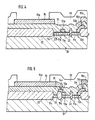
- Fig. 4 is a sectional view along a line A-Aʹ in Fig. 3;
- Fig. 5 is a sectional view along a line B-Bʹ in Fig. 3;
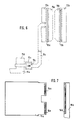
- Fig. 6 is a plan view showing patterns of diffusion regions and polysilicon (polycrystalline silicon) layer;
- Fig. 7 is a plan view showing a pattern of a metal layer; and
- Fig. 8 is a schematic circuit diagram of a protective device according to the present invention.
- Fig. 1 shows a circuit structure of a typical protective device. An input terminal IN is connected to a gate of MOS transistor TR0 to be protected via a resistor R. A drain of a protecting MOS transistor TR1 is connected to a node A of the resistor R with a gate and a source connected to a ground potential. An excessive voltage applied to the input terminal IN is lowered in value by the time constant formed of the resistance of the reisstor R and a stray capacitance Cst of the node A. If the value of the voltage at the node A is still higher than a break-down voltage of the transistor TR1, the transistor TR1 becomes conductive to bypass the excessive charge at the node A to the ground potential. Thus, an excessive voltage applied to the input terminal IN is effectively suppressed by the resistor R and the protective transistor TR1 and destruction of the transistor TR0 is prevented.
- A typical example of a practical structure of the conventional protective device is shown.
- N-
type diffusion regions type semiconductor substrate 10. The N-type regions region 1c. The N-type region 1d is part of a diffusion region of a functional circuit formed with the protective device. Abonding pad 6 as the input terminal formed of ametal pattern 5a of aluminum is connected to an input end of the region 1a via acontact 3a. A wiring 5C made of aluminum is provided with ground potential and connected to theregion 1b throughcontacts 3c. Aninput wiring 5b is connected to theregion 1c viacontacts 3b and to a gate of an input MOS transistor (not shown) such as TR0 in Fig. 1. A wiring 5d made of aluminum is one of wirings connected to the region via acontact 3d. A gate electrode 2 made of a polycrystalline silicon (polysilicon) is connected to the ground wiring 5c. The MOS transistor TR1 thus arranged functions as a punch-through type transistor so that a depletion layer extends and bridges between the drain and thesource regions - Under recent development of integrated circuit fabrication techniques are employed extremely thin gate oxide films which are liable to be damaged by a relatively low excess voltage. This means that the protection circuit should promptly respond to the excess voltage and forcibly lowered the voltage level at the
input wiring 5b. - Experiences to the prior art teach us that high junction leakage currents are not observed after application of an excess voltage five times to the
bonding pad 6. The excess voltage is supplied from a capacitor with a capacitance value of 100 pF through a resistance of 1.5 kΩ after charging the capacitor to 2000 V. - However the effectiveness of this prior art protective device depends on a circuit layout of an integrated circuit fabricated on the same substrate. The protective device has the resistor 1a connected to the
bonding pad 6 at thecontact 3a. When an excess high voltage is applied to thebonding pad 6, the impurity region 1a near thecontact 3a is liable to breakdown. If thesubstrate 10 has theimpurity region 1d with a different voltage level in the vicinity of thecontact 3a, a leakage current concentrates in a limited area of theimpurity region 1d, thereby causing the temperature of thesubstrate 10 around the electric path to rapidly rise. This high temperature results in the destruction of the pn juction of theregion 1d and short-circuits of aluminium leads such as 5d running over the pyrogen due to the softening thereof. Moreover, when the impurity region 1a is forwardly biased under a surge current, the excess voltage reaches to the pn junction formed between thesubstrate 10 and theimpurity region 1d and then destroys the pn junction. Especially, if theimpurity region 1d has a small area with only onecontact 3d connecting theregion 1d to the above conductive layer 5d, the influence of the destruction is extremely serious. - Thus, the
diffusion region 1d must be distant from the region 1a and a certain distance has to be kept therebetween. In other words, the conventional protective device composed of the resistor R and the transistor TR1 must be formed on an area apart from a functional circuit formed on the same semiconductor substrate, as well as its own relatively large size of the protective device. - Thus, the integrated circuit provided with the conventional protective device has the limitation in layout of circuit elements on the same semiconductor substrate and it has been difficult to obtain a high-integration structure of integrated circuit.
- Referring to Figs. 3 to 8, a major part of the integrated circuit according to a preferred embodiment of the present invention is explained.
- The basic circuit structure of the protective device of the present invention is shown in Fig. 8. As shown in Fig. 8, a punch-through type protective transistor TR1ʹ is employed in place of TR1 of Fig. 1 and the transistor TR1ʹ is connected to the input end of the resistor R.
- The protective device is implemented on a P-type silicon substrate 21 (Figs. 3 and 4). In the surface portion of the
silicon substrate 21 are formed N-type diffusion regions type diffusion region 11c (Figs. 3 - 6) extending from a centre portion of a left (outer) side of theregion 11a and serving as the diffusion resistor R. The surfaces of thesediffusion regions insulating film 23 of silicon dioxide except for contact areas and the other surface of the protective device is covered with a thickfield insulating layer 22 of silicon dioxide.Polysilicon connecting layers type diffusion regions contact holes insulating films 23 and extended on the upper surface of the thickinsulating film 22, respectively. Thecontact holes type diffusion regions diffusion regions polysilicon connecting layer 12a is contacted with theregion 11a through the entire length of thecontact hole 13a and its two side portions are extended onto the near-by thick field insulating layer provided adjacently to and along the outer edge of theregion 11a. Thepolysilicon connecting layer 12b is contacting with the N-type diffusion region 11b via the entire length of thecontact hole 13b and extended onto the thick field insulating layer located adjacent to and along the outer edge of theregion 11b. Apolysilicon gate 12c is also formed simultaneously with the polysilicon layers 12a and 12b and forms a functional MOS transistor TR0 to be protected together with N-type source anddrain regions silicon gate 12c is connected to an output end of thediffusion region 11c at a contact hole 13c. - The surface of the
substrate 21 with thepolysilicon layers layer 24 formed of silicon dioxide. Analuminum bonding pad 15a as an input terminal and analuminum wiring 15b are formed on the insulatinglayer 24. Thebonding pad 15a is connected to the two side portions of thepolysilicon layer 12a on the thick field insulating layer throughcontact holes 14a formed in the insulating layer 24 (Figs. 3, 5 and 7) thereby to achieve an electrical connection between theinput terminal 15a and the N-type diffusion region 11a. Thewiring 15b is connected to thepolysilicon layer 12b through acontact hole 14b formed in the insulatinglayer 24 at the location over the thick insulating layer 22 (Figs. 3, 4, 5 and 7) thereby to achieve an electrical connection between thediffusion region 11b and a ground potential which is supplied to thewiring layer 15b. The surface of thesubstrate 21 except abonding area 16 of thebonding pad 15a is covered by an insulatinglayer 25, which may be formed of silicon dioxide, silicon nitride, phosphosilicate glass, or polymid film. - As shown in Figs. 4 and 5, the thick insulating
layer 22 of a thickness of 3000 to 9000 angstroms (favorably 4000 to 7000 angstroms) is provided between the N-type diffusion regions layer 22 therebetween. - The punch-through voltage of this transistor TR1ʹ is favourably in the range of 20 to 40 volts.
- In operation, when an excess voltage is applied to the
bonding pad 15a, the excess voltage propagates through thepolysilicon layer 12a to the N-type region 11a. The N-type region 11a and the N-type region 11b supplied with the ground potential are spaced apart at the relative narrow interval such as 4 microns via the part of the insulatinglayer 22, a depletion layer (not shown) extending from the N-type region 11a applied with the excess voltage reaches the N-type diffusion region 11b. Thus, the electrical path is achieved between thediffusion regions diffusion region 11a to less than a predetermined value. This suppressed voltage is further lowered and moderated through theresistor diffusion region 11c and then applied to thesilicon gate 12c of the transistor TR0 to be protected. In the embodiment, thediffusion regions diffusion regions diffusion regions - Since the
resistor diffusion region 11c is extended from a control portion of the outer edge of thediffusion region 11a towards thebonding pad 15a to run away from the channel of the punch-through transistor TR1ʹ and then bent to run under thebonding pad 15a in the direction normal to the current path of the punch-through transistor TR1ʹ. Therefore, theresistor diffusion region 11c is hardly effected by electric carriers generated at the channel region of the transistor TR1ʹ by the excess voltage. Moreover, an area under thebonding pad 15a is utilized to form theresistor diffusion region 11c, and an area required by the protective device composed of the transistor TR1ʹ and the resistor R can be reduced. - The
polysilicon connecting layers bonding pad 15a and theregion 11a and between thewiring 15b and theregion 11b, respectively. Therefore, even when thebonding pad 15a or thewiring 15b is heated and partially melted by the excess voltage applied to thebonding pad 15a, the melted aluminum is prevented from reaching the surface of thesemiconductor substrate 21 due to presence of the polysilicon layers 12a and 12b. Thus, so-called alloy-spike phenomenon by the melted aluminum can be effectively prevented. - Fig. 6 shows layout patterns of the N-
type diffusion regions polysilicon layers contact holes aluminum layer contact regions - As has been understood from the foregoing description, the protective device according to the present invention is provided with the
diffusion region 11a spacing apart from thediffusion region 11b via the narrow distance such as 4 microns so that the excessive voltage is effectively discharged to the ground regardless of existence of another diffusion region which forms part of a circuit element of the functional circuit fabricated on the same substrate.
Claims (5)
Applications Claiming Priority (2)
| Application Number | Priority Date | Filing Date | Title |
|---|---|---|---|
| JP118760/86 | 1986-05-22 | ||
| JP61118760A JPH065749B2 (en) | 1986-05-22 | 1986-05-22 | Semiconductor device |
Publications (2)
| Publication Number | Publication Date |
|---|---|
| EP0253105A1 true EP0253105A1 (en) | 1988-01-20 |
| EP0253105B1 EP0253105B1 (en) | 1993-03-17 |
Family
ID=14744380
Family Applications (1)
| Application Number | Title | Priority Date | Filing Date |
|---|---|---|---|
| EP87107503A Expired - Lifetime EP0253105B1 (en) | 1986-05-22 | 1987-05-22 | Integrated circuit with improved protective device |
Country Status (4)
| Country | Link |
|---|---|
| US (1) | US4819046A (en) |
| EP (1) | EP0253105B1 (en) |
| JP (1) | JPH065749B2 (en) |
| DE (1) | DE3784793T2 (en) |
Cited By (3)
| Publication number | Priority date | Publication date | Assignee | Title |
|---|---|---|---|---|
| EP0422676A2 (en) * | 1989-10-12 | 1991-04-17 | Nec Corporation | Semiconductor input protection device |
| WO1997004484A1 (en) * | 1995-07-20 | 1997-02-06 | Siemens Aktiengesellschaft | Integrated circuit |
| US5929491A (en) * | 1995-07-20 | 1999-07-27 | Siemens Aktiengesellschaft | Integrated circuit with ESD protection |
Families Citing this family (12)
| Publication number | Priority date | Publication date | Assignee | Title |
|---|---|---|---|---|
| US5066999A (en) * | 1989-10-23 | 1991-11-19 | Micron Technology, Inc. | Resistor under wirebond pad |
| US5121179A (en) * | 1990-10-08 | 1992-06-09 | Seiko Epson Corporation | Higher impedance pull-up and pull-down input protection resistors for MIS transistor integrated circuits |
| JPH03259561A (en) * | 1990-03-09 | 1991-11-19 | Fujitsu Ltd | Semiconductor device |
| US5189638A (en) * | 1990-04-26 | 1993-02-23 | Mitsubishi Denki Kabushiki Kaisha | Portable semiconductor memory device |
| JPH04332163A (en) * | 1991-05-02 | 1992-11-19 | Sony Corp | Semiconductor memory |
| US6002155A (en) * | 1993-02-12 | 1999-12-14 | Fujitsu Limited | Semiconductor integrated circuit with protection circuit against electrostatic breakdown and layout design method therefor |
| WO1996031907A1 (en) * | 1995-04-06 | 1996-10-10 | Industrial Technology Research Institute | N-sided polygonal cell lay-out for multiple cell transistor |
| US5637900A (en) * | 1995-04-06 | 1997-06-10 | Industrial Technology Research Institute | Latchup-free fully-protected CMOS on-chip ESD protection circuit |
| US5572394A (en) * | 1995-04-06 | 1996-11-05 | Industrial Technology Research Institute | CMOS on-chip four-LVTSCR ESD protection scheme |
| US5754380A (en) * | 1995-04-06 | 1998-05-19 | Industrial Technology Research Institute | CMOS output buffer with enhanced high ESD protection capability |
| US6414341B1 (en) * | 1998-09-25 | 2002-07-02 | Nec Corporation | Input/output protective device |
| US7244992B2 (en) * | 2003-07-17 | 2007-07-17 | Ming-Dou Ker | Turn-on-efficient bipolar structures with deep N-well for on-chip ESD protection |
Citations (1)
| Publication number | Priority date | Publication date | Assignee | Title |
|---|---|---|---|---|
| EP0112034A2 (en) * | 1982-12-03 | 1984-06-27 | Fujitsu Limited | A MIS integrated circuit device protected from static charge |
Family Cites Families (9)
| Publication number | Priority date | Publication date | Assignee | Title |
|---|---|---|---|---|
| JPS562663A (en) * | 1979-06-20 | 1981-01-12 | Mitsubishi Electric Corp | Input output protective device for semiconductor ic |
| JPS5715459A (en) * | 1980-07-01 | 1982-01-26 | Fujitsu Ltd | Semiconductor integrated circuit |
| JPS59224164A (en) * | 1983-06-03 | 1984-12-17 | Hitachi Ltd | Electrostatic-breakdown preventing circuit |
| JPS6010765A (en) * | 1983-06-30 | 1985-01-19 | Fujitsu Ltd | Semiconductor device |
| US4605980A (en) * | 1984-03-02 | 1986-08-12 | Zilog, Inc. | Integrated circuit high voltage protection |
| US4692781B2 (en) * | 1984-06-06 | 1998-01-20 | Texas Instruments Inc | Semiconductor device with electrostatic discharge protection |
| JPH0691196B2 (en) * | 1984-07-25 | 1994-11-14 | 株式会社日立製作所 | Semiconductor device |
| JPS6144454A (en) * | 1984-08-09 | 1986-03-04 | Fujitsu Ltd | Semiconductor device |
| US4656732A (en) * | 1984-09-26 | 1987-04-14 | Texas Instruments Incorporated | Integrated circuit fabrication process |
-
1986
- 1986-05-22 JP JP61118760A patent/JPH065749B2/en not_active Expired - Lifetime
-
1987
- 1987-05-22 DE DE8787107503T patent/DE3784793T2/en not_active Expired - Fee Related
- 1987-05-22 EP EP87107503A patent/EP0253105B1/en not_active Expired - Lifetime
- 1987-05-22 US US07/052,923 patent/US4819046A/en not_active Expired - Fee Related
Patent Citations (1)
| Publication number | Priority date | Publication date | Assignee | Title |
|---|---|---|---|---|
| EP0112034A2 (en) * | 1982-12-03 | 1984-06-27 | Fujitsu Limited | A MIS integrated circuit device protected from static charge |
Non-Patent Citations (4)
| Title |
|---|
| PATENT ABSTRACTS OF JAPAN, vol. 6, no. 42 (E-98)[920], 16th March 1982; & JP-A-56 158 481 (RICOH K.K.) 07-12-1981 * |
| PATENT ABSTRACTS OF JAPAN, vol. 9, no. 99 (E-311)[1822], 27th April 1985; & JP-A-59 224 164 (HITACHI SEISAKUSHO K.K.) 17-12-1984 * |
| PROCEEDINGS OF THE 1980 ELECTRICAL OVERSTRESS/ELECTROSTATIC DISCHARGE SYMPOSIUM, pages 73-80; J.K. KELLER: "Protection of MOS integrated circuits from destruction by electrostatic discharge" * |
| PROCEEDINGS OF THE INSTITUTE OF ELECTRICAL AND ELECTRONIC ENGINEERS, vol. 56, no. 7, July 1968, pages 1223-1224, New York, US; R.R. IYER: "Protective device for MOS integrated circuits" * |
Cited By (5)
| Publication number | Priority date | Publication date | Assignee | Title |
|---|---|---|---|---|
| EP0422676A2 (en) * | 1989-10-12 | 1991-04-17 | Nec Corporation | Semiconductor input protection device |
| EP0422676A3 (en) * | 1989-10-12 | 1991-08-07 | Nec Corporation | Semiconductor input protection device |
| WO1997004484A1 (en) * | 1995-07-20 | 1997-02-06 | Siemens Aktiengesellschaft | Integrated circuit |
| US5929491A (en) * | 1995-07-20 | 1999-07-27 | Siemens Aktiengesellschaft | Integrated circuit with ESD protection |
| KR100308074B1 (en) * | 1995-07-20 | 2001-11-17 | 칼 하인쯔 호르닝어 | Integrated circuit |
Also Published As
| Publication number | Publication date |
|---|---|
| DE3784793D1 (en) | 1993-04-22 |
| US4819046A (en) | 1989-04-04 |
| JPS62274664A (en) | 1987-11-28 |
| EP0253105B1 (en) | 1993-03-17 |
| JPH065749B2 (en) | 1994-01-19 |
| DE3784793T2 (en) | 1993-07-08 |
Similar Documents
| Publication | Publication Date | Title |
|---|---|---|
| US5686751A (en) | Electrostatic discharge protection circuit triggered by capacitive-coupling | |
| JP4017187B2 (en) | Electrostatic discharge protection circuit | |
| KR0164908B1 (en) | Semiconductor device having a protective transistor | |
| KR100203054B1 (en) | Electrostatic protecting apparatus | |
| KR0139648B1 (en) | Scr protection structure and circuit with reduced trigger voltage | |
| US4509067A (en) | Semiconductor integrated circuit devices with protective means against overvoltages | |
| US5072273A (en) | Low trigger voltage SCR protection device and structure | |
| US7183612B2 (en) | Semiconductor device having an electrostatic discharge protecting element | |
| KR100645039B1 (en) | Electrostatic discharge protection device and mehtod of fabricating the same | |
| US4819046A (en) | Integrated circuit with improved protective device | |
| US5844280A (en) | Device for protecting a semiconductor circuit | |
| KR19980064705A (en) | Semiconductor devices | |
| KR100194496B1 (en) | Semiconductor devices | |
| US4990984A (en) | Semiconductor device having protective element | |
| JP2965264B2 (en) | Snapback device triggered by low voltage | |
| KR100206675B1 (en) | Semiconductor integrated circuit device | |
| JP2505652B2 (en) | Low trigger voltage SCR protection device and structure | |
| EP0202646B1 (en) | Input protection device | |
| EP0198468A2 (en) | Protective device for integrated circuit | |
| US6534834B1 (en) | Polysilicon bounded snapback device | |
| JPH06236965A (en) | Semiconductor device | |
| US5521413A (en) | Semiconductor device having a solid metal wiring with a contact portion for improved protection | |
| US4727405A (en) | Protective network | |
| KR0165897B1 (en) | Overvoltage protection circuit for mos device | |
| US6870227B1 (en) | Device for protecting against electrostatic discharge |
Legal Events
| Date | Code | Title | Description |
|---|---|---|---|
| PUAI | Public reference made under article 153(3) epc to a published international application that has entered the european phase |
Free format text: ORIGINAL CODE: 0009012 |
|
| 17P | Request for examination filed |
Effective date: 19870522 |
|
| AK | Designated contracting states |
Kind code of ref document: A1 Designated state(s): DE FR GB |
|
| 17Q | First examination report despatched |
Effective date: 19910723 |
|
| GRAA | (expected) grant |
Free format text: ORIGINAL CODE: 0009210 |
|
| AK | Designated contracting states |
Kind code of ref document: B1 Designated state(s): DE FR GB |
|
| REF | Corresponds to: |
Ref document number: 3784793 Country of ref document: DE Date of ref document: 19930422 |
|
| ET | Fr: translation filed | ||
| PLBE | No opposition filed within time limit |
Free format text: ORIGINAL CODE: 0009261 |
|
| STAA | Information on the status of an ep patent application or granted ep patent |
Free format text: STATUS: NO OPPOSITION FILED WITHIN TIME LIMIT |
|
| 26N | No opposition filed | ||
| PGFP | Annual fee paid to national office [announced via postgrant information from national office to epo] |
Ref country code: FR Payment date: 20000510 Year of fee payment: 14 |
|
| PGFP | Annual fee paid to national office [announced via postgrant information from national office to epo] |
Ref country code: GB Payment date: 20000517 Year of fee payment: 14 |
|
| PGFP | Annual fee paid to national office [announced via postgrant information from national office to epo] |
Ref country code: DE Payment date: 20000522 Year of fee payment: 14 |
|
| PG25 | Lapsed in a contracting state [announced via postgrant information from national office to epo] |
Ref country code: GB Free format text: LAPSE BECAUSE OF NON-PAYMENT OF DUE FEES Effective date: 20010522 |
|
| GBPC | Gb: european patent ceased through non-payment of renewal fee |
Effective date: 20010522 |
|
| PG25 | Lapsed in a contracting state [announced via postgrant information from national office to epo] |
Ref country code: FR Free format text: LAPSE BECAUSE OF NON-PAYMENT OF DUE FEES Effective date: 20020131 |
|
| PG25 | Lapsed in a contracting state [announced via postgrant information from national office to epo] |
Ref country code: DE Free format text: LAPSE BECAUSE OF NON-PAYMENT OF DUE FEES Effective date: 20020301 |