JP7661663B2 - 半導体装置及び半導体装置の製造方法 - Google Patents
半導体装置及び半導体装置の製造方法 Download PDFInfo
- Publication number
- JP7661663B2 JP7661663B2 JP2021097292A JP2021097292A JP7661663B2 JP 7661663 B2 JP7661663 B2 JP 7661663B2 JP 2021097292 A JP2021097292 A JP 2021097292A JP 2021097292 A JP2021097292 A JP 2021097292A JP 7661663 B2 JP7661663 B2 JP 7661663B2
- Authority
- JP
- Japan
- Prior art keywords
- conductive pad
- core ball
- conductive
- main surface
- semiconductor device
- Prior art date
- Legal status (The legal status is an assumption and is not a legal conclusion. Google has not performed a legal analysis and makes no representation as to the accuracy of the status listed.)
- Active
Links
Images

Classifications
-
- H—ELECTRICITY
- H10—SEMICONDUCTOR DEVICES; ELECTRIC SOLID-STATE DEVICES NOT OTHERWISE PROVIDED FOR
- H10W—GENERIC PACKAGES, INTERCONNECTIONS, CONNECTORS OR OTHER CONSTRUCTIONAL DETAILS OF DEVICES COVERED BY CLASS H10
- H10W70/00—Package substrates; Interposers; Redistribution layers [RDL]
- H10W70/60—Insulating or insulated package substrates; Interposers; Redistribution layers
- H10W70/67—Insulating or insulated package substrates; Interposers; Redistribution layers characterised by their insulating layers or insulating parts
- H10W70/68—Shapes or dispositions thereof
- H10W70/685—Shapes or dispositions thereof comprising multiple insulating layers
-
- H—ELECTRICITY
- H10—SEMICONDUCTOR DEVICES; ELECTRIC SOLID-STATE DEVICES NOT OTHERWISE PROVIDED FOR
- H10W—GENERIC PACKAGES, INTERCONNECTIONS, CONNECTORS OR OTHER CONSTRUCTIONAL DETAILS OF DEVICES COVERED BY CLASS H10
- H10W72/00—Interconnections or connectors in packages
- H10W72/90—Bond pads, in general
-
- H—ELECTRICITY
- H10—SEMICONDUCTOR DEVICES; ELECTRIC SOLID-STATE DEVICES NOT OTHERWISE PROVIDED FOR
- H10W—GENERIC PACKAGES, INTERCONNECTIONS, CONNECTORS OR OTHER CONSTRUCTIONAL DETAILS OF DEVICES COVERED BY CLASS H10
- H10W70/00—Package substrates; Interposers; Redistribution layers [RDL]
- H10W70/60—Insulating or insulated package substrates; Interposers; Redistribution layers
- H10W70/62—Insulating or insulated package substrates; Interposers; Redistribution layers characterised by their interconnections
- H10W70/65—Shapes or dispositions of interconnections
-
- H—ELECTRICITY
- H10—SEMICONDUCTOR DEVICES; ELECTRIC SOLID-STATE DEVICES NOT OTHERWISE PROVIDED FOR
- H10W—GENERIC PACKAGES, INTERCONNECTIONS, CONNECTORS OR OTHER CONSTRUCTIONAL DETAILS OF DEVICES COVERED BY CLASS H10
- H10W72/00—Interconnections or connectors in packages
- H10W72/01—Manufacture or treatment
- H10W72/012—Manufacture or treatment of bump connectors, dummy bumps or thermal bumps
-
- H—ELECTRICITY
- H10—SEMICONDUCTOR DEVICES; ELECTRIC SOLID-STATE DEVICES NOT OTHERWISE PROVIDED FOR
- H10W—GENERIC PACKAGES, INTERCONNECTIONS, CONNECTORS OR OTHER CONSTRUCTIONAL DETAILS OF DEVICES COVERED BY CLASS H10
- H10W72/00—Interconnections or connectors in packages
- H10W72/01—Manufacture or treatment
- H10W72/016—Manufacture or treatment of strap connectors
-
- H—ELECTRICITY
- H10—SEMICONDUCTOR DEVICES; ELECTRIC SOLID-STATE DEVICES NOT OTHERWISE PROVIDED FOR
- H10W—GENERIC PACKAGES, INTERCONNECTIONS, CONNECTORS OR OTHER CONSTRUCTIONAL DETAILS OF DEVICES COVERED BY CLASS H10
- H10W72/00—Interconnections or connectors in packages
- H10W72/071—Connecting or disconnecting
- H10W72/072—Connecting or disconnecting of bump connectors
- H10W72/07251—Connecting or disconnecting of bump connectors characterised by changes in properties of the bump connectors during connecting
- H10W72/07253—Connecting or disconnecting of bump connectors characterised by changes in properties of the bump connectors during connecting changes in shapes
-
- H—ELECTRICITY
- H10—SEMICONDUCTOR DEVICES; ELECTRIC SOLID-STATE DEVICES NOT OTHERWISE PROVIDED FOR
- H10W—GENERIC PACKAGES, INTERCONNECTIONS, CONNECTORS OR OTHER CONSTRUCTIONAL DETAILS OF DEVICES COVERED BY CLASS H10
- H10W72/00—Interconnections or connectors in packages
- H10W72/20—Bump connectors, e.g. solder bumps or copper pillars; Dummy bumps; Thermal bumps
- H10W72/241—Dispositions, e.g. layouts
- H10W72/245—Dispositions, e.g. layouts of outermost layers of multilayered bumps, e.g. bump coating being only on a part of a bump core
-
- H—ELECTRICITY
- H10—SEMICONDUCTOR DEVICES; ELECTRIC SOLID-STATE DEVICES NOT OTHERWISE PROVIDED FOR
- H10W—GENERIC PACKAGES, INTERCONNECTIONS, CONNECTORS OR OTHER CONSTRUCTIONAL DETAILS OF DEVICES COVERED BY CLASS H10
- H10W72/00—Interconnections or connectors in packages
- H10W72/20—Bump connectors, e.g. solder bumps or copper pillars; Dummy bumps; Thermal bumps
- H10W72/251—Materials
- H10W72/252—Materials comprising solid metals or solid metalloids, e.g. PbSn, Ag or Cu
-
- H—ELECTRICITY
- H10—SEMICONDUCTOR DEVICES; ELECTRIC SOLID-STATE DEVICES NOT OTHERWISE PROVIDED FOR
- H10W—GENERIC PACKAGES, INTERCONNECTIONS, CONNECTORS OR OTHER CONSTRUCTIONAL DETAILS OF DEVICES COVERED BY CLASS H10
- H10W90/00—Package configurations
- H10W90/401—Package configurations characterised by multiple insulating or insulated package substrates, interposers or RDLs
-
- H—ELECTRICITY
- H10—SEMICONDUCTOR DEVICES; ELECTRIC SOLID-STATE DEVICES NOT OTHERWISE PROVIDED FOR
- H10W—GENERIC PACKAGES, INTERCONNECTIONS, CONNECTORS OR OTHER CONSTRUCTIONAL DETAILS OF DEVICES COVERED BY CLASS H10
- H10W70/00—Package substrates; Interposers; Redistribution layers [RDL]
- H10W70/60—Insulating or insulated package substrates; Interposers; Redistribution layers
- H10W70/62—Insulating or insulated package substrates; Interposers; Redistribution layers characterised by their interconnections
- H10W70/63—Vias, e.g. via plugs
- H10W70/635—Through-vias
-
- H—ELECTRICITY
- H10—SEMICONDUCTOR DEVICES; ELECTRIC SOLID-STATE DEVICES NOT OTHERWISE PROVIDED FOR
- H10W—GENERIC PACKAGES, INTERCONNECTIONS, CONNECTORS OR OTHER CONSTRUCTIONAL DETAILS OF DEVICES COVERED BY CLASS H10
- H10W72/00—Interconnections or connectors in packages
- H10W72/90—Bond pads, in general
- H10W72/921—Structures or relative sizes of bond pads
- H10W72/923—Bond pads having multiple stacked layers
-
- H—ELECTRICITY
- H10—SEMICONDUCTOR DEVICES; ELECTRIC SOLID-STATE DEVICES NOT OTHERWISE PROVIDED FOR
- H10W—GENERIC PACKAGES, INTERCONNECTIONS, CONNECTORS OR OTHER CONSTRUCTIONAL DETAILS OF DEVICES COVERED BY CLASS H10
- H10W72/00—Interconnections or connectors in packages
- H10W72/90—Bond pads, in general
- H10W72/951—Materials of bond pads
- H10W72/952—Materials of bond pads comprising metals or metalloids, e.g. PbSn, Ag or Cu
-
- H—ELECTRICITY
- H10—SEMICONDUCTOR DEVICES; ELECTRIC SOLID-STATE DEVICES NOT OTHERWISE PROVIDED FOR
- H10W—GENERIC PACKAGES, INTERCONNECTIONS, CONNECTORS OR OTHER CONSTRUCTIONAL DETAILS OF DEVICES COVERED BY CLASS H10
- H10W90/00—Package configurations
- H10W90/701—Package configurations characterised by the relative positions of pads or connectors relative to package parts
Landscapes
- Electric Connection Of Electric Components To Printed Circuits (AREA)
- Non-Metallic Protective Coatings For Printed Circuits (AREA)
- Production Of Multi-Layered Print Wiring Board (AREA)
- Combinations Of Printed Boards (AREA)
- Engineering & Computer Science (AREA)
- Manufacturing & Machinery (AREA)
- Physics & Mathematics (AREA)
- Geometry (AREA)
- Wire Bonding (AREA)
Description
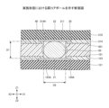
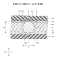
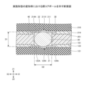
20 銅コアボール
21 第1接触面
22 第2接触面
100 下基板
101 上面
124A、124B 導電パッド
200 上基板
201 下面
211 導電パッド
300 半導体素子
Claims (8)
- 第1主面を有し、前記第1主面に第1導電パッドを備えた第1基板と、
前記第1主面に対向する第2主面を有し、前記第2主面に第2導電パッドを備えた第2基板と、
前記第1基板と前記第2基板との間に配置され、前記第1基板の前記第1主面に実装された半導体素子と、
前記第1導電パッド及び前記第2導電パッドに接触する銅製の導電性コアボールと、
を有し、
前記第1主面に垂直な第1方向における前記導電性コアボールの最大寸法は、前記導電性コアボールの前記第1主面に平行な面内での最大直径よりも小さく、
前記最大寸法は、前記最大直径の85.0%~95.0%であり、
前記導電性コアボールに前記第1方向に平行な圧縮応力が作用しており、
前記導電性コアボールは、
前記第1導電パッドに直接接触する第1接触面と、
前記第2導電パッドに直接接触する第2接触面と、
を有することを特徴とする半導体装置。 - 前記導電性コアボールの形状は楕円体状であることを特徴とする請求項1に記載の半導体装置。
- 前記導電性コアボールの側面を覆うはんだ層を有することを特徴とする請求項1又は2に記載の半導体装置。
- 前記第1導電パッド及び前記第2導電パッドの材料は銅であり、
前記はんだ層は錫を含有し、
前記第1導電パッドと前記はんだ層との間、及び前記第2導電パッドと前記はんだ層との間に、錫及び銅を含有する合金層が存在することを特徴とする請求項3に記載の半導体装置。 - 前記第1接触面の第1直径及び前記第2接触面の第2直径は、前記導電性コアボールの前記最大直径の5.0%~15.0%であることを特徴とする請求項1乃至4のいずれか1項に記載の半導体装置。
- 前記第1導電パッドは、前記導電性コアボールの前記第1接触面の形状に沿って湾曲した第1湾曲部を有することを特徴とする請求項1乃至5のいずれか1項に記載の半導体装置。
- 前記第2導電パッドは、前記導電性コアボールの前記第2接触面の形状に沿って湾曲した第2湾曲部を有することを特徴とする請求項1乃至6のいずれか1項に記載の半導体装置。
- 第1主面を有し、前記第1主面に第1導電パッドを備えた第1基板の前記第1主面に半導体素子を実装する工程と、
第2主面を有し、前記第2主面に第2導電パッドを備えた第2基板の前記第2導電パッドの上に球体状の銅製の導電性コアボールを搭載する工程と、
前記第2主面を前記第1主面に対向させ、前記導電性コアボールを前記第1導電パッド及び前記第2導電パッドに接合する工程と、
を有し、
前記導電性コアボールを前記第1導電パッド及び前記第2導電パッドに接合する工程は、前記導電性コアボールを前記第1主面に垂直な第1方向で圧縮して、前記第1方向における前記導電性コアボールの最大寸法を、前記導電性コアボールの前記第1主面に平行な面内での最大直径よりも小さくする工程を有し、
前記最大寸法を前記最大直径よりも小さくする工程の後において、
前記最大寸法は、前記最大直径の85.0%~95.0%であり、
前記導電性コアボールに前記第1方向に平行な圧縮応力が作用することを特徴とする半導体装置の製造方法。
Priority Applications (4)
| Application Number | Priority Date | Filing Date | Title |
|---|---|---|---|
| JP2021097292A JP7661663B2 (ja) | 2021-06-10 | 2021-06-10 | 半導体装置及び半導体装置の製造方法 |
| US17/805,302 US12406953B2 (en) | 2021-06-10 | 2022-06-03 | Semiconductor apparatus and method of making semiconductor apparatus |
| CN202210638855.1A CN115472589A (zh) | 2021-06-10 | 2022-06-07 | 半导体装置及半导体装置的制造方法 |
| KR1020220069339A KR20220167226A (ko) | 2021-06-10 | 2022-06-08 | 반도체 장치 및 반도체 장치의 제조 방법 |
Applications Claiming Priority (1)
| Application Number | Priority Date | Filing Date | Title |
|---|---|---|---|
| JP2021097292A JP7661663B2 (ja) | 2021-06-10 | 2021-06-10 | 半導体装置及び半導体装置の製造方法 |
Publications (3)
| Publication Number | Publication Date |
|---|---|
| JP2022188977A JP2022188977A (ja) | 2022-12-22 |
| JP2022188977A5 JP2022188977A5 (ja) | 2024-04-11 |
| JP7661663B2 true JP7661663B2 (ja) | 2025-04-15 |
Family
ID=84363399
Family Applications (1)
| Application Number | Title | Priority Date | Filing Date |
|---|---|---|---|
| JP2021097292A Active JP7661663B2 (ja) | 2021-06-10 | 2021-06-10 | 半導体装置及び半導体装置の製造方法 |
Country Status (4)
| Country | Link |
|---|---|
| US (1) | US12406953B2 (ja) |
| JP (1) | JP7661663B2 (ja) |
| KR (1) | KR20220167226A (ja) |
| CN (1) | CN115472589A (ja) |
Families Citing this family (1)
| Publication number | Priority date | Publication date | Assignee | Title |
|---|---|---|---|---|
| US20250323136A1 (en) * | 2024-04-12 | 2025-10-16 | Qualcomm Incorporated | Integrated circuit (ic) package including two substrates and vertical interconnects coupling the two substrates, the vertical interconnects comprising a metal ball and metal pin combination to address an increased distance between substrates |
Citations (3)
| Publication number | Priority date | Publication date | Assignee | Title |
|---|---|---|---|---|
| WO2007069606A1 (ja) | 2005-12-14 | 2007-06-21 | Shinko Electric Industries Co., Ltd. | チップ内蔵基板およびチップ内蔵基板の製造方法 |
| JP2011187635A (ja) | 2010-03-08 | 2011-09-22 | Hitachi Metals Ltd | 半導体装置およびその製造方法 |
| JP2012099642A (ja) | 2010-11-02 | 2012-05-24 | Hitachi Metals Ltd | 半導体装置、それを用いた電子部品およびそれらの製造方法 |
Family Cites Families (10)
| Publication number | Priority date | Publication date | Assignee | Title |
|---|---|---|---|---|
| JP3270813B2 (ja) * | 1995-07-11 | 2002-04-02 | 株式会社ピーエフユー | 半導体装置とその製造方法 |
| US5926694A (en) * | 1996-07-11 | 1999-07-20 | Pfu Limited | Semiconductor device and a manufacturing method thereof |
| JPH10270496A (ja) * | 1997-03-27 | 1998-10-09 | Hitachi Ltd | 電子装置、情報処理装置、半導体装置並びに半導体チップの実装方法 |
| US6610591B1 (en) * | 2000-08-25 | 2003-08-26 | Micron Technology, Inc. | Methods of ball grid array |
| US20080142968A1 (en) * | 2006-12-15 | 2008-06-19 | International Business Machines Corporation | Structure for controlled collapse chip connection with a captured pad geometry |
| JP5525793B2 (ja) * | 2009-10-19 | 2014-06-18 | パナソニック株式会社 | 半導体装置 |
| JP5421863B2 (ja) | 2010-06-28 | 2014-02-19 | 新光電気工業株式会社 | 半導体パッケージの製造方法 |
| US20130043573A1 (en) * | 2011-08-15 | 2013-02-21 | Advanced Analogic Technologies (Hong Kong) Limited | Solder Bump Bonding In Semiconductor Package Using Solder Balls Having High-Temperature Cores |
| JP6352644B2 (ja) * | 2014-02-12 | 2018-07-04 | 新光電気工業株式会社 | 配線基板及び半導体パッケージの製造方法 |
| US10157850B1 (en) * | 2017-07-28 | 2018-12-18 | Taiwan Semiconductor Manufacturing Co., Ltd. | Semiconductor packages and manufacturing method thereof |
-
2021
- 2021-06-10 JP JP2021097292A patent/JP7661663B2/ja active Active
-
2022
- 2022-06-03 US US17/805,302 patent/US12406953B2/en active Active
- 2022-06-07 CN CN202210638855.1A patent/CN115472589A/zh active Pending
- 2022-06-08 KR KR1020220069339A patent/KR20220167226A/ko active Pending
Patent Citations (3)
| Publication number | Priority date | Publication date | Assignee | Title |
|---|---|---|---|---|
| WO2007069606A1 (ja) | 2005-12-14 | 2007-06-21 | Shinko Electric Industries Co., Ltd. | チップ内蔵基板およびチップ内蔵基板の製造方法 |
| JP2011187635A (ja) | 2010-03-08 | 2011-09-22 | Hitachi Metals Ltd | 半導体装置およびその製造方法 |
| JP2012099642A (ja) | 2010-11-02 | 2012-05-24 | Hitachi Metals Ltd | 半導体装置、それを用いた電子部品およびそれらの製造方法 |
Also Published As
| Publication number | Publication date |
|---|---|
| KR20220167226A (ko) | 2022-12-20 |
| CN115472589A (zh) | 2022-12-13 |
| JP2022188977A (ja) | 2022-12-22 |
| US20220399293A1 (en) | 2022-12-15 |
| US12406953B2 (en) | 2025-09-02 |
Similar Documents
| Publication | Publication Date | Title |
|---|---|---|
| JP6408986B2 (ja) | Bvaインタポーザ | |
| US11482500B2 (en) | Method of forming an electronic device structure having an electronic component with an on-edge orientation and related structures | |
| JP2009514237A (ja) | 金属立方形半導体デバイスおよび方法 | |
| CN101145545A (zh) | 包括元件安装表面被树脂层涂覆的布线基板的半导体装置 | |
| JP2007103737A (ja) | 半導体装置 | |
| JP2015153816A (ja) | 配線基板、半導体パッケージ及び半導体パッケージの製造方法 | |
| JP2008085089A (ja) | 樹脂配線基板および半導体装置 | |
| JP2017174849A (ja) | 半導体装置及び半導体装置の製造方法 | |
| WO2006064863A1 (ja) | プリント配線板 | |
| JP7661663B2 (ja) | 半導体装置及び半導体装置の製造方法 | |
| JP2009111307A (ja) | 部品内蔵配線板 | |
| CN111755409A (zh) | 半导体封装基板及其制法与电子封装件及其制法 | |
| KR101394647B1 (ko) | 반도체 패키지 및 그 제조방법 | |
| JP2008153536A (ja) | 電子部品内蔵基板および電子部品内蔵基板の製造方法 | |
| EP4090141A1 (en) | Composite wiring substrate, semiconductor device, and method of manufacturing composite wiring substrate | |
| KR100744138B1 (ko) | 볼 그리드 어레이 반도체 패키지 및 그의 제조방법 | |
| TW201507097A (zh) | 半導體晶片及具有半導體晶片之半導體裝置 | |
| KR101391108B1 (ko) | 반도체 패키지 제조방법 | |
| KR102960137B1 (ko) | 반도체 장치 | |
| US12438074B2 (en) | Semiconductor apparatus | |
| CN114975296B (zh) | 半导体结构及其制造方法 | |
| JP5934057B2 (ja) | プリント回路基板 | |
| JP2011029669A (ja) | 半導体装置 | |
| JP2008135483A (ja) | 電子部品内蔵基板およびその製造方法 | |
| JP5411981B2 (ja) | 半導体装置の製造方法 |
Legal Events
| Date | Code | Title | Description |
|---|---|---|---|
| A521 | Request for written amendment filed |
Free format text: JAPANESE INTERMEDIATE CODE: A523 Effective date: 20240403 |
|
| A621 | Written request for application examination |
Free format text: JAPANESE INTERMEDIATE CODE: A621 Effective date: 20240403 |
|
| A977 | Report on retrieval |
Free format text: JAPANESE INTERMEDIATE CODE: A971007 Effective date: 20241129 |
|
| A131 | Notification of reasons for refusal |
Free format text: JAPANESE INTERMEDIATE CODE: A131 Effective date: 20241203 |
|
| A521 | Request for written amendment filed |
Free format text: JAPANESE INTERMEDIATE CODE: A523 Effective date: 20250128 |
|
| TRDD | Decision of grant or rejection written | ||
| A01 | Written decision to grant a patent or to grant a registration (utility model) |
Free format text: JAPANESE INTERMEDIATE CODE: A01 Effective date: 20250304 |
|
| A61 | First payment of annual fees (during grant procedure) |
Free format text: JAPANESE INTERMEDIATE CODE: A61 Effective date: 20250312 |
|
| R150 | Certificate of patent or registration of utility model |
Ref document number: 7661663 Country of ref document: JP Free format text: JAPANESE INTERMEDIATE CODE: R150 |