JP7661663B2 - Semiconductor device and method for manufacturing the same - Google Patents
Semiconductor device and method for manufacturing the same Download PDFInfo
- Publication number
- JP7661663B2 JP7661663B2 JP2021097292A JP2021097292A JP7661663B2 JP 7661663 B2 JP7661663 B2 JP 7661663B2 JP 2021097292 A JP2021097292 A JP 2021097292A JP 2021097292 A JP2021097292 A JP 2021097292A JP 7661663 B2 JP7661663 B2 JP 7661663B2
- Authority
- JP
- Japan
- Prior art keywords
- conductive pad
- core ball
- conductive
- main surface
- semiconductor device
- Prior art date
- Legal status (The legal status is an assumption and is not a legal conclusion. Google has not performed a legal analysis and makes no representation as to the accuracy of the status listed.)
- Active
Links
Images

Classifications
-
- H—ELECTRICITY
- H10—SEMICONDUCTOR DEVICES; ELECTRIC SOLID-STATE DEVICES NOT OTHERWISE PROVIDED FOR
- H10W—GENERIC PACKAGES, INTERCONNECTIONS, CONNECTORS OR OTHER CONSTRUCTIONAL DETAILS OF DEVICES COVERED BY CLASS H10
- H10W70/00—Package substrates; Interposers; Redistribution layers [RDL]
- H10W70/60—Insulating or insulated package substrates; Interposers; Redistribution layers
- H10W70/67—Insulating or insulated package substrates; Interposers; Redistribution layers characterised by their insulating layers or insulating parts
- H10W70/68—Shapes or dispositions thereof
- H10W70/685—Shapes or dispositions thereof comprising multiple insulating layers
-
- H—ELECTRICITY
- H10—SEMICONDUCTOR DEVICES; ELECTRIC SOLID-STATE DEVICES NOT OTHERWISE PROVIDED FOR
- H10W—GENERIC PACKAGES, INTERCONNECTIONS, CONNECTORS OR OTHER CONSTRUCTIONAL DETAILS OF DEVICES COVERED BY CLASS H10
- H10W72/00—Interconnections or connectors in packages
- H10W72/90—Bond pads, in general
-
- H—ELECTRICITY
- H10—SEMICONDUCTOR DEVICES; ELECTRIC SOLID-STATE DEVICES NOT OTHERWISE PROVIDED FOR
- H10W—GENERIC PACKAGES, INTERCONNECTIONS, CONNECTORS OR OTHER CONSTRUCTIONAL DETAILS OF DEVICES COVERED BY CLASS H10
- H10W70/00—Package substrates; Interposers; Redistribution layers [RDL]
- H10W70/60—Insulating or insulated package substrates; Interposers; Redistribution layers
- H10W70/62—Insulating or insulated package substrates; Interposers; Redistribution layers characterised by their interconnections
- H10W70/65—Shapes or dispositions of interconnections
-
- H—ELECTRICITY
- H10—SEMICONDUCTOR DEVICES; ELECTRIC SOLID-STATE DEVICES NOT OTHERWISE PROVIDED FOR
- H10W—GENERIC PACKAGES, INTERCONNECTIONS, CONNECTORS OR OTHER CONSTRUCTIONAL DETAILS OF DEVICES COVERED BY CLASS H10
- H10W72/00—Interconnections or connectors in packages
- H10W72/01—Manufacture or treatment
- H10W72/012—Manufacture or treatment of bump connectors, dummy bumps or thermal bumps
-
- H—ELECTRICITY
- H10—SEMICONDUCTOR DEVICES; ELECTRIC SOLID-STATE DEVICES NOT OTHERWISE PROVIDED FOR
- H10W—GENERIC PACKAGES, INTERCONNECTIONS, CONNECTORS OR OTHER CONSTRUCTIONAL DETAILS OF DEVICES COVERED BY CLASS H10
- H10W72/00—Interconnections or connectors in packages
- H10W72/01—Manufacture or treatment
- H10W72/016—Manufacture or treatment of strap connectors
-
- H—ELECTRICITY
- H10—SEMICONDUCTOR DEVICES; ELECTRIC SOLID-STATE DEVICES NOT OTHERWISE PROVIDED FOR
- H10W—GENERIC PACKAGES, INTERCONNECTIONS, CONNECTORS OR OTHER CONSTRUCTIONAL DETAILS OF DEVICES COVERED BY CLASS H10
- H10W72/00—Interconnections or connectors in packages
- H10W72/071—Connecting or disconnecting
- H10W72/072—Connecting or disconnecting of bump connectors
- H10W72/07251—Connecting or disconnecting of bump connectors characterised by changes in properties of the bump connectors during connecting
- H10W72/07253—Connecting or disconnecting of bump connectors characterised by changes in properties of the bump connectors during connecting changes in shapes
-
- H—ELECTRICITY
- H10—SEMICONDUCTOR DEVICES; ELECTRIC SOLID-STATE DEVICES NOT OTHERWISE PROVIDED FOR
- H10W—GENERIC PACKAGES, INTERCONNECTIONS, CONNECTORS OR OTHER CONSTRUCTIONAL DETAILS OF DEVICES COVERED BY CLASS H10
- H10W72/00—Interconnections or connectors in packages
- H10W72/20—Bump connectors, e.g. solder bumps or copper pillars; Dummy bumps; Thermal bumps
- H10W72/241—Dispositions, e.g. layouts
- H10W72/245—Dispositions, e.g. layouts of outermost layers of multilayered bumps, e.g. bump coating being only on a part of a bump core
-
- H—ELECTRICITY
- H10—SEMICONDUCTOR DEVICES; ELECTRIC SOLID-STATE DEVICES NOT OTHERWISE PROVIDED FOR
- H10W—GENERIC PACKAGES, INTERCONNECTIONS, CONNECTORS OR OTHER CONSTRUCTIONAL DETAILS OF DEVICES COVERED BY CLASS H10
- H10W72/00—Interconnections or connectors in packages
- H10W72/20—Bump connectors, e.g. solder bumps or copper pillars; Dummy bumps; Thermal bumps
- H10W72/251—Materials
- H10W72/252—Materials comprising solid metals or solid metalloids, e.g. PbSn, Ag or Cu
-
- H—ELECTRICITY
- H10—SEMICONDUCTOR DEVICES; ELECTRIC SOLID-STATE DEVICES NOT OTHERWISE PROVIDED FOR
- H10W—GENERIC PACKAGES, INTERCONNECTIONS, CONNECTORS OR OTHER CONSTRUCTIONAL DETAILS OF DEVICES COVERED BY CLASS H10
- H10W90/00—Package configurations
- H10W90/401—Package configurations characterised by multiple insulating or insulated package substrates, interposers or RDLs
-
- H—ELECTRICITY
- H10—SEMICONDUCTOR DEVICES; ELECTRIC SOLID-STATE DEVICES NOT OTHERWISE PROVIDED FOR
- H10W—GENERIC PACKAGES, INTERCONNECTIONS, CONNECTORS OR OTHER CONSTRUCTIONAL DETAILS OF DEVICES COVERED BY CLASS H10
- H10W70/00—Package substrates; Interposers; Redistribution layers [RDL]
- H10W70/60—Insulating or insulated package substrates; Interposers; Redistribution layers
- H10W70/62—Insulating or insulated package substrates; Interposers; Redistribution layers characterised by their interconnections
- H10W70/63—Vias, e.g. via plugs
- H10W70/635—Through-vias
-
- H—ELECTRICITY
- H10—SEMICONDUCTOR DEVICES; ELECTRIC SOLID-STATE DEVICES NOT OTHERWISE PROVIDED FOR
- H10W—GENERIC PACKAGES, INTERCONNECTIONS, CONNECTORS OR OTHER CONSTRUCTIONAL DETAILS OF DEVICES COVERED BY CLASS H10
- H10W72/00—Interconnections or connectors in packages
- H10W72/90—Bond pads, in general
- H10W72/921—Structures or relative sizes of bond pads
- H10W72/923—Bond pads having multiple stacked layers
-
- H—ELECTRICITY
- H10—SEMICONDUCTOR DEVICES; ELECTRIC SOLID-STATE DEVICES NOT OTHERWISE PROVIDED FOR
- H10W—GENERIC PACKAGES, INTERCONNECTIONS, CONNECTORS OR OTHER CONSTRUCTIONAL DETAILS OF DEVICES COVERED BY CLASS H10
- H10W72/00—Interconnections or connectors in packages
- H10W72/90—Bond pads, in general
- H10W72/951—Materials of bond pads
- H10W72/952—Materials of bond pads comprising metals or metalloids, e.g. PbSn, Ag or Cu
-
- H—ELECTRICITY
- H10—SEMICONDUCTOR DEVICES; ELECTRIC SOLID-STATE DEVICES NOT OTHERWISE PROVIDED FOR
- H10W—GENERIC PACKAGES, INTERCONNECTIONS, CONNECTORS OR OTHER CONSTRUCTIONAL DETAILS OF DEVICES COVERED BY CLASS H10
- H10W90/00—Package configurations
- H10W90/701—Package configurations characterised by the relative positions of pads or connectors relative to package parts
Landscapes
- Electric Connection Of Electric Components To Printed Circuits (AREA)
- Non-Metallic Protective Coatings For Printed Circuits (AREA)
- Production Of Multi-Layered Print Wiring Board (AREA)
- Combinations Of Printed Boards (AREA)
- Engineering & Computer Science (AREA)
- Manufacturing & Machinery (AREA)
- Physics & Mathematics (AREA)
- Geometry (AREA)
- Wire Bonding (AREA)
Description
本開示は、半導体装置及び半導体装置の製造方法に関する。 This disclosure relates to a semiconductor device and a method for manufacturing a semiconductor device.
銅コアボールをスペーサ部材として用いて上基板と下基板とを接続した半導体パッケージが開示されている(特許文献1)。 A semiconductor package is disclosed in which an upper substrate and a lower substrate are connected using copper core balls as spacer members (Patent Document 1).
特許文献1に記載の半導体パッケージによれば、所期の目的は達成されるものの、銅コアボールと下基板及び上基板との間により高い接続信頼性が望まれる。 Although the semiconductor package described in Patent Document 1 achieves the intended purpose, higher connection reliability between the copper core ball and the lower and upper substrates is desired.
本開示は、接続信頼性を向上することができる半導体装置及び半導体装置の製造方法を提供することを目的とする。 The present disclosure aims to provide a semiconductor device and a method for manufacturing a semiconductor device that can improve connection reliability.
本開示の一形態によれば、第1主面を有し、前記第1主面に第1導電パッドを備えた第1基板と、前記第1主面に対向する第2主面を有し、前記第2主面に第2導電パッドを備えた第2基板と、前記第1基板と前記第2基板との間に配置され、前記第1基板の前記第1主面に実装された半導体素子と、前記第1導電パッド及び前記第2導電パッドに接触する銅製の導電性コアボールと、を有し、前記第1主面に垂直な第1方向における前記導電性コアボールの最大寸法は、前記導電性コアボールの前記第1主面に平行な面内での最大直径よりも小さく、前記最大寸法は、前記最大直径の85.0%~95.0%であり、前記導電性コアボールに前記第1方向に平行な圧縮応力が作用しており、前記導電性コアボールは、前記第1導電パッドに直接接触する第1接触面と、前記第2導電パッドに直接接触する第2接触面と、を有する半導体装置が提供される。 According to one aspect of the present disclosure, there is provided a semiconductor device comprising: a first substrate having a first main surface and a first conductive pad on the first main surface; a second substrate having a second main surface opposite to the first main surface and a second conductive pad on the second main surface; a semiconductor element mounted on the first main surface of the first substrate and disposed between the first substrate and the second substrate; and a copper conductive core ball in contact with the first conductive pad and the second conductive pad, wherein a maximum dimension of the conductive core ball in a first direction perpendicular to the first main surface is smaller than a maximum diameter of the conductive core ball in a plane parallel to the first main surface, the maximum dimension being 85.0% to 95.0% of the maximum diameter, a compressive stress parallel to the first direction is acting on the conductive core ball, and the conductive core ball has a first contact surface in direct contact with the first conductive pad and a second contact surface in direct contact with the second conductive pad.
開示の技術によれば、接続信頼性を向上することができる。 The disclosed technology can improve connection reliability.
以下、実施形態について添付の図面を参照しながら具体的に説明する。なお、本明細書及び図面において、実質的に同一の機能構成を有する構成要素については、同一の符号を付することにより重複した説明を省くことがある。また、本開示においては、X1-X2方向、Y1-Y2方向、Z1-Z2方向を相互に直交する方向とする。X1-X2方向及びY1-Y2方向を含む面をXY面と記載し、Y1-Y2方向及びZ1-Z2方向を含む面をYZ面と記載し、Z1-Z2方向及びX1-X2方向を含む面をZX面と記載する。なお、便宜上、Z1-Z2方向を上下方向とし、Z1側を上側、Z2側を下側とする。また、平面視とは、Z1側から対象物を視ることをいい、平面形状とは、対象物をZ1側から視た形状のことをいう。但し、半導体装置は天地逆の状態で用いることができ、又は任意の角度で配置することができる。 The following describes the embodiments in detail with reference to the attached drawings. In this specification and the drawings, components having substantially the same functional configuration may be denoted by the same reference numerals to avoid repetitive description. In this disclosure, the X1-X2 direction, the Y1-Y2 direction, and the Z1-Z2 direction are defined as mutually orthogonal directions. A plane including the X1-X2 direction and the Y1-Y2 direction is described as the XY plane, a plane including the Y1-Y2 direction and the Z1-Z2 direction is described as the YZ plane, and a plane including the Z1-Z2 direction and the X1-X2 direction is described as the ZX plane. For convenience, the Z1-Z2 direction is defined as the up-down direction, the Z1 side is defined as the upper side, and the Z2 side is defined as the lower side. In addition, a planar view refers to viewing an object from the Z1 side, and a planar shape refers to the shape of an object viewed from the Z1 side. However, the semiconductor device can be used upside down or can be arranged at any angle.
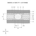
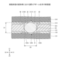
本実施形態は、半導体装置及びその製造方法に関する。図1は、実施形態に係る半導体装置を示す断面図である。 This embodiment relates to a semiconductor device and a manufacturing method thereof. Figure 1 is a cross-sectional view showing a semiconductor device according to the embodiment.
実施形態に係る半導体装置10は、下基板100と、上基板200と、半導体素子300とを有する。下基板100はXY面に略平行な上面101を有し、上基板200はXY面に略平行な下面201を有する。上基板200は下基板100の上側(Z1側)に配置されている。上基板200の下面201が下基板100の上面101に対向している。下基板100は第1基板の一例であり、上基板200は第2基板の一例である。下基板100の上面101は第1主面の一例であり、上基板200の下面201は第2主面の一例である。
The
下基板100は、例えば、コア層110と、コア層110の上面に設けられたビルドアップ層120と、コア層110の下面に設けられたビルドアップ層130とを有する。下基板100が、コア層を含まないコアレス基板であってもよい。
The
コア層110は、貫通孔114が形成された絶縁性の基材111と、貫通孔114の内壁面に形成された貫通導電ビア112と、貫通導電ビア112の内側に充填された充填材113とを有する。例えば、コア層110の材料はガラスエポキシ等であり、貫通導電ビア112の材料は銅等である。
The
ビルドアップ層120は、絶縁層121と、配線層122と、ソルダレジスト層123とを有する。ソルダレジスト層123には、上基板200との接続用の開口部123Aと、半導体素子300の実装用の開口部123Bとが形成されている。配線層122は、絶縁層121の最上面に、上基板200との接続用の導電パッド124Aと、半導体素子300の実装用の導電パッド124Bとを含む。導電パッド124Aは開口部123Aから露出し、導電パッド124Bは開口部123Bから露出する。配線層122の材料は、例えば銅等の導電体である。導電パッド124Aは第1導電パッドの一例である。
The build-up
ビルドアップ層130は、絶縁層131と、配線層132と、ソルダレジスト層133とを有する。ソルダレジスト層133には、外部接続用の開口部133Aが形成されている。配線層132は、絶縁層131の最下面に導電パッド134を含む。導電パッド134は開口部133Aから露出する。配線層132の材料は、例えば銅等の導電体である。導電パッド134上にはんだボール135が設けられている。
The build-up
導電パッド124Aと、導電パッド124Bと、導電パッド134とが、配線層122、貫通導電ビア112及び配線層132を介して電気的に接続されている。ビルドアップ層120に含まれる絶縁層121及び配線層122の数、ビルドアップ層130に含まれる絶縁層131及び配線層132の数は特に限定されない。
The
半導体素子300は下基板100の上面101にフリップチップ実装されている。すなわち、半導体素子300のバンプ301が接合材310を介して下基板100の導電パッド124Bに電気的に接続されている。接合材310は、例えばはんだから構成される。半導体素子300と下基板100との間にはアンダーフィル材320が充填されている。
The
上基板200は、例えば、コア層210と、導電パッド211と、導電パッド212と、ソルダレジスト層214と、ソルダレジスト層215とを有する。
The
導電パッド211はコア層210の下面に設けられており、導電パッド212はコア層210の上面に設けられている。導電パッド212は、コア層210に形成されたビアホール213を通じて導電パッド211に接続されている。導電パッド211及び導電パッド212の材料は、例えば銅等の導電体である。導電パッド211は第2導電パッドの一例である。
The
ソルダレジスト層214はコア層210の下面を覆っている。ソルダレジスト層214には、下基板100との接続用の開口部214Aが形成されている。導電パッド211は開口部214Aから露出する。ソルダレジスト層215はコア層210の上面を覆っている。ソルダレジスト層215には、外部接続用の開口部215Aが形成されている。導電パッド212は開口部215Aから露出する。導電パッド212は、半導体素子、受動素子又は他の配線基板等の電子部品を上基板200に搭載するために用いられる。
The
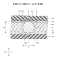
半導体装置10は、下基板100の導電パッド124Aと上基板200の導電パッド211とに接触する銅(Cu)コアボール20を有する。ここで、銅コアボール20について詳細に説明する。図2は、銅コアボール20を示す断面図である。
The
下基板100の導電パッド124Aと、上基板200の導電パッド211とは互いに対向している。そして、銅コアボール20は、導電パッド124A及び導電パッド211の両方に接触している。銅コアボール20は、導電パッド124Aに直接接触する第1接触面21と、導電パッド211に直接接触する第2接触面22とを有する。銅コアボール20は、下基板100の上面101に垂直な第1方向、すなわちZ1-Z2方向における最大寸法D1と、上面101に平行な面、すなわちXY面に平行な面内での最大直径D2とを有し、最大寸法D1は最大直径D2よりも小さい。最大寸法D1は、Z1-Z2方向における銅コアボール20の寸法の最大値である。最大寸法D1は、いわば銅コアボール20の高さである。最大直径D2は、XY面に平行な面内での銅コアボール20の直径の最大値である。例えば、最大寸法D1は、最大直径D2の90%程度である。銅コアボール20の表面にNi層が形成されていてもよい。
The
銅コアボール20の形状は楕円体状であってもよい。本開示における楕円体状とは、数学的に定義される厳密な楕円体を意味するものではない。銅コアボール20が楕円体状である場合、最大寸法D1は楕円体の短径に相当し、最大直径D2は楕円体の長径に相当する。第1接触面21及び第2接触面22は平坦な面であってもよく、銅コアボール20の中心から外側に向かって凸状になった曲面であってもよい。
The shape of the
第1接触面21及び第2接触面22の平面形状は円形状である。第1接触面21の第1直径及び第2接触面22の第2直径は、最大直径D2の10%程度である。また、第1接触面21の第1面積及び第2接触面22の第2面積は、銅コアボール20のXY面に平行な断面積のうち最大の断面積(最大断面積)の1%程度である。
The planar shape of the
銅コアボール20の側面ははんだ層30により覆われている。はんだ層30は導電パッド124A及び導電パッド211の両方に接触していてもよい。はんだ層30の材料は、例えば、Sn(錫)、Sn-Ag(銀)系、Sn-Cu系、Sn-Ag-Cu系のPb(鉛)フリーはんだである。
The side of the
上基板200と下基板100との間にモールド樹脂40が充填され、上基板200は下基板100に対して固定されている。上基板200と下基板100との間の距離は銅コアボール20により維持されている。
次に、実施形態に係る半導体装置10の製造方法について説明する。図3~図8は、実施形態に係る半導体装置10の製造方法を示す断面図である。
Next, a method for manufacturing the
まず、図3に示すように、下基板100を準備する。上述のように、下基板100は、導電パッド124A及び導電パッド124B等を有する。次いで、導電パッド124Bの上に、例えば接合材310を形成する。接合材310は、電解めっき法等により形成することができる。
First, as shown in FIG. 3, the
次いで、図4に示すように、バンプ301が形成された半導体素子300を下基板100にフリップチップ実装する。すなわち、接合材310を介してバンプ301を下基板100の導電パッド124Bに電気的に接続する。次いで、半導体素子300と下基板100との間にアンダーフィル材320を充填する。
Next, as shown in FIG. 4, the
また、図5に示すように、上基板200を準備する。上述のように、上基板200は、導電パッド211等を有する。次いで、銅コア付きはんだボール24を導電パッド211の上に搭載する。銅コア付きはんだボール24は、球体状の銅コアボール23と、銅コアボール23の外周に設けられたはんだ層30とを有する。本開示における球体状とは、数学的に定義される厳密な球体を意味するものではない。銅コアボール23の表面にNi層が形成されていてもよい。
As shown in FIG. 5, the
半導体素子300と下基板100との間へのアンダーフィル材320の充填と、銅コア付きはんだボール24の搭載の後、図6に示すように、下基板100と上基板200との間にモールド樹脂40を設けながら、銅コア付きはんだボール24が導電パッド124Aに接するようにして、上基板200を下基板100の上に載置する。半導体素子300は、下基板100と上基板200との間に配置される。
After filling the gap between the
次いで、図6に示す下基板100及び上基板200を含む積層構造体をZ1-Z2方向で圧縮しながら、はんだ層30のリフローを行う。この結果、図7に示すように、球体状の銅コアボール23がZ1-Z2方向で圧縮されて楕円体状の銅コアボール20が形成される。また、はんだ層30の成分(例えば錫)と、導電パッド124Aの成分(例えば銅)及び導電パッド211の成分(例えば銅)とから合金層(図示せず)が形成される。リフローの温度は、例えば260℃程度である。
Then, the
次いで、図8に示すように、導電パッド134の上にはんだボール135を形成する。
Next, as shown in FIG. 8,
このようにして、実施形態に係る半導体装置10を製造することができる。
In this manner, the
なお、上基板200を下基板100の上に載置する際にモールド樹脂40を設けずに、楕円体状の銅コアボール20が形成された後にモールド樹脂40を設けてもよい。また、上基板200を下基板100の上に載置する際にモールド樹脂40を設けずに、図6に示す下基板100及び上基板200を含む積層構造体をZ1-Z2方向で圧縮する際にモールド樹脂40を設けてもよい。
In addition, the
ここで、本実施形態の効果について、参考例と比較しながら説明する。図9は、参考例における銅コアボールを示す断面図である。 Here, the effects of this embodiment will be explained in comparison with a reference example. Figure 9 is a cross-sectional view showing a copper core ball in the reference example.
参考例では、図9に示すように、銅コアボール20に代えて、球体状の銅コアボール25が設けられている。銅コアボール25は球体状であるため、銅コアボール25のZ1-Z2方向における最大寸法D3は、銅コアボール25のXY面に平行な面内での最大直径D4と等しい。銅コアボール25は導電パッド124Aに接触する第1接触点26と、導電パッド211に接触する第2接触点27とを有する。他の構成は、本実施形態と同様である。
In the reference example, as shown in FIG. 9, a spherical
本実施形態に係る半導体装置10では、銅コアボール20のZ1-Z2方向における最大寸法D1が、銅コアボール20のXY面に平行な面内での最大直径D2よりも小さく、銅コアボール20が導電パッド124Aに接触する第1接触面21と、導電パッド211に接触する第2接触面22とを有する。
In the
このように、参考例では、銅コアボール25が点で導電パッド124A及び導電パッド211に接触するのに対し、本実施形態では、銅コアボール20が面で導電パッド124A及び導電パッド211に接触する。このため、本実施形態によれば、参考例と比較して、銅コアボール20と、下基板100及び上基板200との間に高い接続信頼性を得ることができる。
Thus, in the reference example, the
また、上述のように、はんだ層30のリフローの際に合金層が形成される。合金層の形成に伴ってはんだ層30の体積が減少するが、本実施形態によれば、はんだ層30の体積が減少したとしても、優れた接続信頼性を得ることができる。
As described above, an alloy layer is formed when the
また、本実施形態では、球体状の銅コアボール23が圧縮されて楕円体状の銅コアボール20が形成される際に、はんだ層30が導電パッド124Aの上及び導電パッド211の上で広がる。つまり、はんだ層30が広く導電パッド124A及び導電パッド211に接触する。このため、合金層の形成に伴ってはんだ層30の体積が減少したとしても、下基板100と上基板200との間の接続を強固に維持することができる。
In addition, in this embodiment, when the spherical
また、下基板100及び上基板200の反り等に起因して、はんだ層30のリフロー前に、導電パッド124Aと導電パッド211との間の距離にばらつきが生じていることがある。この場合、参考例では、銅コアボール25が導電パッド124A又は導電パッド211に接触できないおそれがある。一方、本実施形態では、導電パッド124Aと導電パッド211との間に銅コアボール23を挟み、銅コアボール23を圧縮して銅コアボール20としているため、銅コアボール20を導電パッド124A及び導電パッド211により確実に接触させることができる。更に、銅コアボール23と銅コアボール25のサイズが同一であれば、本実施形態では、半導体装置10の高さ(Z1-Z2方向の寸法)を小さくすることができる。
In addition, due to warping of the
なお、銅コアボール23の圧縮の際に導電パッド124A及び導電パッド211も変形してよい。また、銅コアボール20が導電パッド124A及び導電パッド211にめり込んでいてもよい。銅コアボール20が導電パッド124A及び導電パッド211にめり込んでいる場合、第1接触面21及び第2接触面22が曲面となりやすく、第1接触面21及び第2接触面22が平坦面の場合と比較して、第1接触面21及び第2接触面22の面積を大きく確保しやすい。
The
例えば、図10に示すように、銅コアボール20の第1接触面21及び第2接触面22が曲面となっていてもよい。また、導電パッド124Aが第1接触面21の形状に沿って湾曲した第1湾曲部124Xを有してもよく、導電パッド211が第2接触面22の形状に沿って湾曲した第2湾曲部211Xを有してもよい。図10は、実施形態の変形例における銅コアボールを示す断面図である。
For example, as shown in FIG. 10, the
最大寸法D1は、最大直径D2の、好ましくは80.0%~99.9%であり、より好ましくは85.0%~95.0%である。最大寸法D1の最大直径D2に対する比が小さいほど、第1接触面21及び第2接触面22の面積を大きく確保しやすい。一方、最大寸法D1の最大直径D2に対する比が小さすぎる場合、下基板100と上基板200との間に適切な距離を確保しながら、銅コアボール20同士の間の短絡を抑制することが困難になるおそれがある。
The maximum dimension D1 is preferably 80.0% to 99.9% of the maximum diameter D2, and more preferably 85.0% to 95.0%. The smaller the ratio of the maximum dimension D1 to the maximum diameter D2, the easier it is to ensure a large area for the
第1接触面21の第1直径及び第2接触面22の第2直径は、最大直径D2の、好ましくは0.1%~20.0%であり、より好ましくは5.0%~15.0%である。第1直径及び第2直径の最大直径D2に対する比が大きいほど、第1接触面21及び第2接触面22の面積を大きく確保しやすい。一方、第1直径及び第2直径の最大直径D2に対する比を大きくするためには、銅コアボール23をより強い力で圧縮する必要があり、加工が困難になるおそれがある。第1接触面21の第1直径、第2接触面22の第2直径の少なくとも一方が上記の好ましい範囲にあれば、接続信頼性を向上しやすく、少なくとも一方が上記のより好ましい範囲にあれば、接続信頼性を更に向上しやすい。
The first diameter of the
以上、好ましい実施の形態等について詳説したが、上述した実施の形態等に制限されることはなく、特許請求の範囲に記載された範囲を逸脱することなく、上述した実施の形態等に種々の変形及び置換を加えることができる。 Although the preferred embodiments have been described above in detail, the present invention is not limited to the above-described embodiments, and various modifications and substitutions can be made to the above-described embodiments without departing from the scope of the claims.
10 半導体装置
20 銅コアボール
21 第1接触面
22 第2接触面
100 下基板
101 上面
124A、124B 導電パッド
200 上基板
201 下面
211 導電パッド
300 半導体素子
REFERENCE SIGNS
Claims (8)
前記第1主面に対向する第2主面を有し、前記第2主面に第2導電パッドを備えた第2基板と、
前記第1基板と前記第2基板との間に配置され、前記第1基板の前記第1主面に実装された半導体素子と、
前記第1導電パッド及び前記第2導電パッドに接触する銅製の導電性コアボールと、
を有し、
前記第1主面に垂直な第1方向における前記導電性コアボールの最大寸法は、前記導電性コアボールの前記第1主面に平行な面内での最大直径よりも小さく、
前記最大寸法は、前記最大直径の85.0%~95.0%であり、
前記導電性コアボールに前記第1方向に平行な圧縮応力が作用しており、
前記導電性コアボールは、
前記第1導電パッドに直接接触する第1接触面と、
前記第2導電パッドに直接接触する第2接触面と、
を有することを特徴とする半導体装置。 a first substrate having a first major surface and a first conductive pad on the first major surface;
a second substrate having a second main surface opposite to the first main surface and having a second conductive pad on the second main surface;
a semiconductor element disposed between the first substrate and the second substrate and mounted on the first main surface of the first substrate;
a copper conductive core ball in contact with the first conductive pad and the second conductive pad;
having
a maximum dimension of the conductive core ball in a first direction perpendicular to the first main surface is smaller than a maximum diameter of the conductive core ball in a plane parallel to the first main surface;
the maximum dimension is between 85.0% and 95.0% of the maximum diameter;
A compressive stress parallel to the first direction is applied to the conductive core ball,
The conductive core ball is
a first contact surface in direct contact with the first conductive pad;
a second contact surface in direct contact with the second conductive pad;
A semiconductor device comprising:
前記はんだ層は錫を含有し、the solder layer contains tin;
前記第1導電パッドと前記はんだ層との間、及び前記第2導電パッドと前記はんだ層との間に、錫及び銅を含有する合金層が存在することを特徴とする請求項3に記載の半導体装置。4. The semiconductor device according to claim 3, wherein an alloy layer containing tin and copper is present between the first conductive pad and the solder layer and between the second conductive pad and the solder layer.
第2主面を有し、前記第2主面に第2導電パッドを備えた第2基板の前記第2導電パッドの上に球体状の銅製の導電性コアボールを搭載する工程と、
前記第2主面を前記第1主面に対向させ、前記導電性コアボールを前記第1導電パッド及び前記第2導電パッドに接合する工程と、
を有し、
前記導電性コアボールを前記第1導電パッド及び前記第2導電パッドに接合する工程は、前記導電性コアボールを前記第1主面に垂直な第1方向で圧縮して、前記第1方向における前記導電性コアボールの最大寸法を、前記導電性コアボールの前記第1主面に平行な面内での最大直径よりも小さくする工程を有し、
前記最大寸法を前記最大直径よりも小さくする工程の後において、
前記最大寸法は、前記最大直径の85.0%~95.0%であり、
前記導電性コアボールに前記第1方向に平行な圧縮応力が作用することを特徴とする半導体装置の製造方法。 a step of mounting a semiconductor element on a first main surface of a first substrate having a first main surface and a first conductive pad on the first main surface;
a step of mounting a spherical copper conductive core ball on a second conductive pad of a second substrate having a second main surface and a second conductive pad on the second main surface;
a step of bonding the conductive core ball to the first conductive pad and the second conductive pad while facing the second main surface to the first main surface;
having
the step of joining the conductive core ball to the first conductive pad and the second conductive pad includes a step of compressing the conductive core ball in a first direction perpendicular to the first main surface to make a maximum dimension of the conductive core ball in the first direction smaller than a maximum diameter of the conductive core ball in a plane parallel to the first main surface;
After the step of reducing the maximum dimension to less than the maximum diameter,
the maximum dimension is between 85.0% and 95.0% of the maximum diameter;
A method for manufacturing a semiconductor device, comprising the steps of: applying a compressive stress parallel to the first direction to the conductive core ball .
Priority Applications (4)
| Application Number | Priority Date | Filing Date | Title |
|---|---|---|---|
| JP2021097292A JP7661663B2 (en) | 2021-06-10 | 2021-06-10 | Semiconductor device and method for manufacturing the same |
| US17/805,302 US12406953B2 (en) | 2021-06-10 | 2022-06-03 | Semiconductor apparatus and method of making semiconductor apparatus |
| CN202210638855.1A CN115472589A (en) | 2021-06-10 | 2022-06-07 | Semiconductor device and method for manufacturing semiconductor device |
| KR1020220069339A KR20220167226A (en) | 2021-06-10 | 2022-06-08 | Semiconductor apparatus and method of making semiconductor apparatus |
Applications Claiming Priority (1)
| Application Number | Priority Date | Filing Date | Title |
|---|---|---|---|
| JP2021097292A JP7661663B2 (en) | 2021-06-10 | 2021-06-10 | Semiconductor device and method for manufacturing the same |
Publications (3)
| Publication Number | Publication Date |
|---|---|
| JP2022188977A JP2022188977A (en) | 2022-12-22 |
| JP2022188977A5 JP2022188977A5 (en) | 2024-04-11 |
| JP7661663B2 true JP7661663B2 (en) | 2025-04-15 |
Family
ID=84363399
Family Applications (1)
| Application Number | Title | Priority Date | Filing Date |
|---|---|---|---|
| JP2021097292A Active JP7661663B2 (en) | 2021-06-10 | 2021-06-10 | Semiconductor device and method for manufacturing the same |
Country Status (4)
| Country | Link |
|---|---|
| US (1) | US12406953B2 (en) |
| JP (1) | JP7661663B2 (en) |
| KR (1) | KR20220167226A (en) |
| CN (1) | CN115472589A (en) |
Families Citing this family (1)
| Publication number | Priority date | Publication date | Assignee | Title |
|---|---|---|---|---|
| US20250323136A1 (en) * | 2024-04-12 | 2025-10-16 | Qualcomm Incorporated | Integrated circuit (ic) package including two substrates and vertical interconnects coupling the two substrates, the vertical interconnects comprising a metal ball and metal pin combination to address an increased distance between substrates |
Citations (3)
| Publication number | Priority date | Publication date | Assignee | Title |
|---|---|---|---|---|
| WO2007069606A1 (en) | 2005-12-14 | 2007-06-21 | Shinko Electric Industries Co., Ltd. | Substrate with built-in chip and method for manufacturing substrate with built-in chip |
| JP2011187635A (en) | 2010-03-08 | 2011-09-22 | Hitachi Metals Ltd | Semiconductor device, and method of manufacturing the same |
| JP2012099642A (en) | 2010-11-02 | 2012-05-24 | Hitachi Metals Ltd | Semiconductor device, electronic component using the same, and method of manufacturing them |
Family Cites Families (10)
| Publication number | Priority date | Publication date | Assignee | Title |
|---|---|---|---|---|
| JP3270813B2 (en) * | 1995-07-11 | 2002-04-02 | 株式会社ピーエフユー | Semiconductor device and manufacturing method thereof |
| US5926694A (en) * | 1996-07-11 | 1999-07-20 | Pfu Limited | Semiconductor device and a manufacturing method thereof |
| JPH10270496A (en) * | 1997-03-27 | 1998-10-09 | Hitachi Ltd | Electronic device, information processing device, semiconductor device, and semiconductor chip mounting method |
| US6610591B1 (en) * | 2000-08-25 | 2003-08-26 | Micron Technology, Inc. | Methods of ball grid array |
| US20080142968A1 (en) * | 2006-12-15 | 2008-06-19 | International Business Machines Corporation | Structure for controlled collapse chip connection with a captured pad geometry |
| JP5525793B2 (en) * | 2009-10-19 | 2014-06-18 | パナソニック株式会社 | Semiconductor device |
| JP5421863B2 (en) | 2010-06-28 | 2014-02-19 | 新光電気工業株式会社 | Manufacturing method of semiconductor package |
| US20130043573A1 (en) * | 2011-08-15 | 2013-02-21 | Advanced Analogic Technologies (Hong Kong) Limited | Solder Bump Bonding In Semiconductor Package Using Solder Balls Having High-Temperature Cores |
| JP6352644B2 (en) * | 2014-02-12 | 2018-07-04 | 新光電気工業株式会社 | Wiring substrate and semiconductor package manufacturing method |
| US10157850B1 (en) * | 2017-07-28 | 2018-12-18 | Taiwan Semiconductor Manufacturing Co., Ltd. | Semiconductor packages and manufacturing method thereof |
-
2021
- 2021-06-10 JP JP2021097292A patent/JP7661663B2/en active Active
-
2022
- 2022-06-03 US US17/805,302 patent/US12406953B2/en active Active
- 2022-06-07 CN CN202210638855.1A patent/CN115472589A/en active Pending
- 2022-06-08 KR KR1020220069339A patent/KR20220167226A/en active Pending
Patent Citations (3)
| Publication number | Priority date | Publication date | Assignee | Title |
|---|---|---|---|---|
| WO2007069606A1 (en) | 2005-12-14 | 2007-06-21 | Shinko Electric Industries Co., Ltd. | Substrate with built-in chip and method for manufacturing substrate with built-in chip |
| JP2011187635A (en) | 2010-03-08 | 2011-09-22 | Hitachi Metals Ltd | Semiconductor device, and method of manufacturing the same |
| JP2012099642A (en) | 2010-11-02 | 2012-05-24 | Hitachi Metals Ltd | Semiconductor device, electronic component using the same, and method of manufacturing them |
Also Published As
| Publication number | Publication date |
|---|---|
| KR20220167226A (en) | 2022-12-20 |
| CN115472589A (en) | 2022-12-13 |
| JP2022188977A (en) | 2022-12-22 |
| US20220399293A1 (en) | 2022-12-15 |
| US12406953B2 (en) | 2025-09-02 |
Similar Documents
| Publication | Publication Date | Title |
|---|---|---|
| JP6408986B2 (en) | BVA interposer | |
| US11482500B2 (en) | Method of forming an electronic device structure having an electronic component with an on-edge orientation and related structures | |
| JP2009514237A (en) | Metal cubic semiconductor device and method | |
| CN101145545A (en) | Semiconductor device including a wiring substrate whose component mounting surface is coated with a resin layer | |
| JP2007103737A (en) | Semiconductor device | |
| JP2015153816A (en) | Wiring substrate, semiconductor package, and manufacturing method of semiconductor package | |
| JP2008085089A (en) | Resin wiring board and semiconductor device | |
| JP2017174849A (en) | Semiconductor device and semiconductor device manufacturing method | |
| WO2006064863A1 (en) | Printed wiring board | |
| JP7661663B2 (en) | Semiconductor device and method for manufacturing the same | |
| JP2009111307A (en) | Component built-in wiring board | |
| CN111755409A (en) | Semiconductor packaging substrate and its manufacturing method and electronic package and its manufacturing method | |
| KR101394647B1 (en) | Semiconductor package and method for fabricating the same | |
| JP2008153536A (en) | Electronic component built-in substrate and method for manufacturing electronic component built-in substrate | |
| EP4090141A1 (en) | Composite wiring substrate, semiconductor device, and method of manufacturing composite wiring substrate | |
| KR100744138B1 (en) | Ball Grid Array Semiconductor Package and Manufacturing Method Thereof | |
| TW201507097A (en) | Semiconductor wafer and semiconductor device having the same | |
| KR101391108B1 (en) | Method for manufacturing semiconductor chip pakage | |
| KR102960137B1 (en) | Semiconductor apparatus | |
| US12438074B2 (en) | Semiconductor apparatus | |
| CN114975296B (en) | Semiconductor structure and manufacturing method | |
| JP5934057B2 (en) | Printed circuit board | |
| JP2011029669A (en) | Semiconductor device | |
| JP2008135483A (en) | Substrate incorporating electronic component and its manufacturing method | |
| JP5411981B2 (en) | Manufacturing method of semiconductor device |
Legal Events
| Date | Code | Title | Description |
|---|---|---|---|
| A521 | Request for written amendment filed |
Free format text: JAPANESE INTERMEDIATE CODE: A523 Effective date: 20240403 |
|
| A621 | Written request for application examination |
Free format text: JAPANESE INTERMEDIATE CODE: A621 Effective date: 20240403 |
|
| A977 | Report on retrieval |
Free format text: JAPANESE INTERMEDIATE CODE: A971007 Effective date: 20241129 |
|
| A131 | Notification of reasons for refusal |
Free format text: JAPANESE INTERMEDIATE CODE: A131 Effective date: 20241203 |
|
| A521 | Request for written amendment filed |
Free format text: JAPANESE INTERMEDIATE CODE: A523 Effective date: 20250128 |
|
| TRDD | Decision of grant or rejection written | ||
| A01 | Written decision to grant a patent or to grant a registration (utility model) |
Free format text: JAPANESE INTERMEDIATE CODE: A01 Effective date: 20250304 |
|
| A61 | First payment of annual fees (during grant procedure) |
Free format text: JAPANESE INTERMEDIATE CODE: A61 Effective date: 20250312 |
|
| R150 | Certificate of patent or registration of utility model |
Ref document number: 7661663 Country of ref document: JP Free format text: JAPANESE INTERMEDIATE CODE: R150 |