以下、添付図面を参照して、本願の開示する基板処理装置および基板処理方法の実施形態を詳細に説明する。なお、以下に示す実施形態により本開示が限定されるものではない。また、図面は模式的なものであり、各要素の寸法の関係、各要素の比率などは、現実と異なる場合があることに留意する必要がある。さらに、図面の相互間においても、互いの寸法の関係や比率が異なる部分が含まれている場合がある。
従来、半導体ウェハ(以下、ウェハとも呼称する。)などの基板を複数まとめて浸漬処理するバッチ処理において、かかる処理に用いられた処理液に含まれる成分の濃度を検出する技術が知られている。
一方で、基板を一枚ずつ回転させながら処理液を吐出して液処理する枚葉処理において、かかる処理に用いられた処理液に含まれる成分の濃度を精度よく検出することは非常に困難である。なぜなら、基板上に形成される液膜の膜厚が非常に薄いため、基板上の処理液を測定した場合、成分の濃度を精度よく検出するための測定長が十分に取れないからである。
そこで、上述の問題点を克服し、基板の枚葉処理に用いられた処理液に含まれる成分の濃度を精度よく検出することができる技術の実現が期待されている。
<基板処理システムの概要>
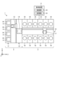
最初に、図1を参照しながら、実施形態に係る基板処理システム1の概略構成について説明する。図1は、実施形態に係る基板処理システム1の概略構成を示す図である。かかる基板処理システム1は、基板処理装置の一例である。以下では、位置関係を明確にするために、互いに直交するX軸、Y軸およびZ軸を規定し、Z軸正方向を鉛直上向き方向とする。
図1に示すように、基板処理システム1は、搬入出ステーション2と、処理ステーション3とを備える。搬入出ステーション2と処理ステーション3とは隣接して設けられる。
搬入出ステーション2は、フープ載置部11と、搬送部12とを備える。フープ載置部11には、複数枚の基板、実施形態では半導体ウェハW(以下、ウェハWと呼称する。)を水平状態で収容する複数のフープHが載置される。
搬送部12は、フープ載置部11に隣接して設けられ、内部に基板搬送装置13と、受渡部14とを備える。基板搬送装置13は、ウェハWを保持するウェハ保持機構を備える。また、基板搬送装置13は、水平方向および鉛直方向への移動ならびに鉛直軸を中心とする旋回が可能であり、ウェハ保持機構を用いてフープHと受渡部14との間でウェハWの搬送を行う。
処理ステーション3は、搬送部12に隣接して設けられる。処理ステーション3は、搬送部15と、複数の処理ユニット16とを備える。複数の処理ユニット16は、搬送部15の両側に並べて設けられる。
搬送部15は、内部に基板搬送装置17を備える。基板搬送装置17は、ウェハWを保持するウェハ保持機構を備える。また、基板搬送装置17は、水平方向および鉛直方向への移動ならびに鉛直軸を中心とする旋回が可能であり、ウェハ保持機構を用いて受渡部14と処理ユニット16との間でウェハWの搬送を行う。
処理ユニット16は、基板搬送装置17によって搬送されるウェハWに対して所定の基板処理を行う。
また、基板処理システム1は、制御装置4を備える。制御装置4は、たとえばコンピュータであり、制御部18と記憶部19とを備える。記憶部19には、基板処理システム1において実行される各種の処理を制御するプログラムが格納される。制御部18は、記憶部19に記憶されたプログラムを読み出して実行することによって基板処理システム1の動作を制御する。
なお、かかるプログラムは、コンピュータによって読み取り可能な記憶媒体に記録されていたものであって、その記憶媒体から制御装置4の記憶部19にインストールされたものであってもよい。コンピュータによって読み取り可能な記憶媒体としては、たとえばハードディスク(HD)、フレキシブルディスク(FD)、コンパクトディスク(CD)、マグネットオプティカルディスク(MO)、メモリカードなどがある。
上記のように構成された基板処理システム1では、まず、搬入出ステーション2の基板搬送装置13が、フープ載置部11に載置されたフープHからウェハWを取り出し、取り出したウェハWを受渡部14に載置する。受渡部14に載置されたウェハWは、処理ステーション3の基板搬送装置17によって受渡部14から取り出されて、処理ユニット16へ搬入される。
処理ユニット16へ搬入されたウェハWは、処理ユニット16によって処理された後、基板搬送装置17によって処理ユニット16から搬出されて、受渡部14に載置される。そして、受渡部14に載置された処理済のウェハWは、基板搬送装置13によってフープ載置部11のフープHへ戻される。
<処理ユニットの構成>
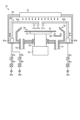
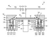
次に、分析部60が搭載される処理ユニット16の構成について、図2を参照しながら説明する。図2は、処理ユニット16の具体的な構成の一例を示す模式図である。図2に示すように、処理ユニット16は、チャンバ20と、基板処理部30と、液供給部40と、回収カップ50と、分析部60とを備える。
チャンバ20は、基板処理部30と、液供給部40と、回収カップ50と、分析部60とを収容する。チャンバ20の天井部には、FFU(Fan Filter Unit)21が設けられる。FFU21は、チャンバ20内にダウンフローを形成する。
基板処理部30は、保持部31と、支柱部32と、駆動部33とを備え、載置されたウェハWに液処理を施す。保持部31は、ウェハWを水平に保持する。支柱部32は、鉛直方向に延在する部材であり、基端部が駆動部33によって回転可能に支持され、先端部において保持部31を水平に支持する。駆動部33は、支柱部32を鉛直軸まわりに回転させる。
かかる基板処理部30は、駆動部33を用いて支柱部32を回転させることによって支柱部32に支持された保持部31を回転させ、これにより、保持部31に保持されたウェハWを回転させる。
保持部31は、たとえば、ウェハWの下面を吸着することにより、かかるウェハWを水平に保持する。なお、保持部31は、吸着チャックに限られず、静電チャックなどであってもよい。なお、ウェハWは、基板処理が行われる表面を上方に向けた状態で保持部31に保持される。
液供給部40は、ウェハWに対して処理流体を供給する。液供給部40は、ノズル41a、41bと、ノズル41a、41bを水平に支持するアーム42aと、アーム42aを旋回および昇降させる旋回昇降機構43aとを備える。
また、液供給部40は、ノズル41cと、ノズル41cを水平に支持するアーム42bと、アーム42bを旋回および昇降させる旋回昇降機構43bとを備える。
ノズル41aは、バルブ44aおよび流量調整器45aを介してDHF供給源46aに接続される。DHF供給源46aは、たとえば、DHF(希フッ酸)を貯留するタンクである。かかるDHFは、処理液の一例である。
ノズル41bは、バルブ44bおよび流量調整器45bを介してIPA供給源46bに接続される。IPA供給源46bは、たとえば、IPA(IsoPropyl Alcohol)を貯留するタンクである。かかるIPAは、処理液の別の一例である。
ノズル41cは、バルブ44cおよび流量調整器45cを介してDIW供給源46cに接続される。DIW供給源46cは、たとえば、DIW(DeIonized Water:脱イオン水)を貯留するタンクである。かかるDIWは、処理液のさらに別の一例である。
ノズル41aからは、DHF供給源46aより供給されるDHFが吐出される。ノズル41bからは、IPA供給源46bより供給されるIPAが吐出される。ノズル41cからは、DIW供給源46cより供給されるDIWが吐出される。
回収カップ50は、保持部31を取り囲むように配置され、保持部31の回転によってウェハWから飛散する処理液S(図3参照)を捕集する。回収カップ50の底部には、排液口51が形成されており、回収カップ50によって捕集された処理液Sは、かかる排液口51から処理ユニット16の外部へ排出される。また、回収カップ50の底部には、FFU21から供給される気体を処理ユニット16の外部へ排出する排気口52が形成される。
分析部60は、保持部31の回転によってウェハWから流れ出る処理液Sに含まれる成分の濃度を検出する。分析部60は、たとえば、ウェハWの縁部よりも外側かつ回収カップ50よりも内側に配置される。また、分析部60は、保持部31に保持されるウェハWよりも低い位置に配置される。
<分析部の構成>
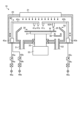
次に、実施形態に係る分析部60の構成について、図3を参照しながら説明する。図3は、実施形態に係る分析部60の構成の一例を示す図である。
図3に示すように、実施形態に係る分析部60は、液受け部61と、濃度センサ62とを備える。液受け部61は、回転しながら液処理が施されるウェハW(図2参照)から流れ出る処理液Sを受ける。濃度センサ62は、液受け部61内に滞留する処理液Sに含まれる成分の濃度を検出する。
実施形態に係る濃度センサ62は、たとえば、赤外分光法によって処理液Sに含まれる成分の濃度を検出する。濃度センサ62は、投光部62aおよび受光部62bを有する。
投光部62aは、たとえば、光ファイバ(図示せず)によって赤外線光源(図示せず)と接続される。投光部62aは、かかる赤外線光源から供給される赤外光IRを、液受け部61の被測定部65を介して受光部62bに照射する。
受光部62bは、たとえば、光ファイバ(図示せず)によって測光部(図示せず)と接続される。受光部62bは、投光部62aから液受け部61の被測定部65を介して照射された赤外光IRを受光し、かかる受光した光を測光部に送る。かかる測光部は、受光した赤外光IRを分光し、そのデータを制御部18(図1参照)に送る。
物質は、それぞれ固有の吸収スペクトルを有する。制御部18は、赤外光IRの吸収スペクトルから、測定したい成分に応じた所定波長における吸光度を求め、かかる成分の濃度を算出することができる。
たとえば、測光部で得られた赤外光IRの吸収スペクトルにおいて、波長1460(nm)付近には、H2OのOH結合に起因する吸収のピークが認められる。また、波長1690(nm)付近には、IPAのCH結合に起因する2つの吸収ピークが認められる。
そこで、処理液SにおけるH2Oの濃度を検出したい場合には、波長約1460(nm)付近のOH基の吸収ピークにおける吸光度Aに着目すればよい。なお、波長1460(nm)付近はOH基の伸縮振動の倍音であり、波長1690(nm)付近はCH基の伸縮振動の倍音である。
吸光度Aは、ランベルト・ベールの法則により、以下の式(1)で表される。
A=αLC ・・・(1)
A:吸光度
α:吸光係数
L:測定長
C:濃度
上記の式(1)に基づけば、検出対象となる成分の吸光係数αおよび測定長Lが既知であれば、濃度Cの値を求めることができる。そして、実施形態では、図3に示すように、投光部62aと受光部62bとの間の距離L0が測定長Lとなる。
一方で、吸光係数αは共存する成分の影響等を受けて変化するため、実際の処理条件に近い条件において、測定長Lが等しい処理液Sを用いて測定を行って検量線を作成し、その検量線に基づいて濃度Cの値を算出するのが好ましい。
実施形態では、濃度センサ62の赤外線光源が、連続する波長範囲の赤外光IRを発生するとよい。これにより、制御部18の設定を変更するだけで、多くの成分の濃度検出に対応することができる。
また、検出する成分が定まっている場合でも、吸収ピーク波長は共存する周囲の物質によってシフトする場合があるため、連続した波長の赤外光IRを用いるほうが、より高精度での測定が可能となる。このような光源としては、ハロゲンタングステンランプなどの市販のものを用いることができる。
なお、赤外線光源が発生する赤外光IRは、単一の波長であってもよい。たとえば、赤外線光源は、波長可変レーザであってもよいし、干渉フィルタなどを用いて目的とする成分の吸収ピーク波長を選択的に取り出すものであってもよい。また、投光部62aに、バンドパスフィルタである干渉フィルタを設置して、所望の波長の赤外光IRを照射してもよい。
このように、単一の波長の赤外光IRを用いることにより、制御部18における演算処理を単純にすることができることから、演算速度を速くすることができる。
投光部62aは、コリメータなどを用いて平行光線を投光できることが好ましいが、光学系の明るさを確保するために受光部62bに集光する光線を投光できてもよい。
受光部62bに接続される測光部は、受光部62bから光ファイバによって導かれた赤外光IRを必要に応じて分光し、検出して電気信号に変換し、必要に応じて増幅等の処理を行う。
かかる測光部の構造は特に限定されず、回折格子等を用いた分散型分光光度計、フーリエ変換赤外分光光度計等の非分散型分光光度計など、公知のものを用いることができる。なお、投光部62aから特定の波長の赤外光IRが投光される場合は、測光部での分光手段は不要である。
制御部18は、測光部からの電気信号に基づいて、吸収スペクトルや所定波長における吸光度を計算する。また、制御部18は、吸光度を積算による平均化処理あるいは、単位時間内に度数分布を作成して、メディアン値(中央値)を求めて、測定データのばらつきを抑える処理を行う。その後、制御部18は、濃度演算等を行う。
連続する波長範囲の赤外光IRを用いる場合、その波長範囲は、検出対象となる成分が吸収する波長を含む必要がある。たとえば、H2OとIPAとを測定する場合、好ましくは、1350(nm)~1720(nm)を含む波長範囲の赤外光IRを照射する。
また、H2Oの濃度を測定するための吸収ピークは、前述の波長1460(nm)付近の他に、波長1200(nm)付近、波長1900(nm)付近、波長2600(nm)付近にも存在する。波長1200(nm)付近の吸収ピークは吸光係数が小さいが、波長1900(nm)および波長2600(nm)付近の吸収ピークは吸光係数が大きいため、かかる吸収ピークを用いてもよい。
図3の説明に戻る。液受け部61は、流入口63と、排出口64と、被測定部65とを有する。流入口63は、ウェハWから流れ出る処理液Sが流入する。排出口64は、液受け部61の内部に滞留する処理液Sを排出する。かかる排出口64は、流入口63よりも低い位置に配置される。
被測定部65は、濃度センサ62によって処理液Sが測定される部位である。すなわち、被測定部65は、投光部62aと受光部62bとの間に位置し、測定用の赤外光IRが通過する部位である。被測定部65は、流入口63よりも低く、かつ排出口64よりも高い位置に配置される。
ここで、実施形態では、回転しながら液処理が施されるウェハWから流れ出る処理液Sを一旦液受け部61で受けて、かかる液受け部61において処理液Sに含まれる成分の濃度を濃度センサ62で検出する。
これにより、ウェハW上に形成される処理液Sの液膜に対して赤外光を照射して濃度を検出する場合と比べて、成分の濃度を精度よく検出するための測定長Lを十分に取ることができる。
したがって、実施形態によれば、ウェハWの枚葉処理に用いられた処理液Sに含まれる成分の濃度を精度よく検出することができる。
なお、実施形態において、測定長Lは、たとえば、1(mm)以上であるとよく、10(mm)以上であるとより好ましい。これにより、ウェハWの枚葉処理に用いられた処理液Sに含まれる成分の濃度をさらに精度よく検出することができる。
また、実施形態では、液受け部61が、被測定部65よりも高い位置に流入口63を有し、被測定部65よりも低い位置に排出口64を有する。これにより、液受け部61で受けた処理液Sが被測定部65で澱まないように、常に外部に流れるようにすることができる。
したがって、実施形態によれば、ウェハWの枚葉処理において、かかるウェハWから流れ出る処理液Sの成分濃度の時間経過を連続的に検出することができる。
また、実施形態では、ウェハWの液処理時において、被測定部65に処理液Sが常時滞留するように、流入口63および排出口64の大きさが適宜設定されるとよい。これにより、ウェハWの液処理の最初から最後まで、処理液Sの成分濃度の時間経過を連続的に検出することができる。
たとえば、実施形態に係るウェハWの液処理では、最初にDHFによる基板処理が行われ、次にDIWによるリンス処理が行われ、次にIPAによる乾燥処理が行われる。
そして、DIWによるリンス処理では、処理液Sに含まれるDHFの濃度を分析部60で検出することにより、かかるリンス処理の終点検知が可能となる。さらに、IPAによる乾燥処理では、処理液Sに含まれるDIWの濃度を検出することにより、かかる乾燥処理の終点検知が可能となる。すなわち、実施形態では、余分な時間の液処理を省くことができる。
したがって、実施形態によれば、処理ユニット16に分析部60が設けられることにより、ウェハWの全体的な処理時間を短くすることができることから、ウェハWを効率的に液処理することができる。
また、実施形態では、余分な液処理を省くことができることから、使用済みの処理液Sの排液処理コストや、処理液Sの準備コストなどを低減することができる。
なお、実施形態に係るウェハWの液処理は、上記の例に限られず、2種類以上の成分が処理液S内で混ざった状態となる液処理であれば適用可能である。
実施形態に係るウェハWの液処理に用いられる薬液としては、たとえば、HF(フッ酸)、NH4OH(アンモニア水)、H2SO4(硫酸)、H2O2(過酸化水素水)、HCl(塩酸)、NH4F(フッ化アンモニウム)などが挙げられる。
また、実施形態に係るウェハWの液処理では、HNO3(硝酸)、H3PO4(リン酸)、TMAH(水酸化テトラメチルアンモニウム)などが用いられてもよい。
また、実施形態に係る液処理の終点検知処理は、上記の例に限られず、たとえば、エッチング液によるエッチング処理において、処理液S中のエッチング対象となる成分の濃度を検出することにより、エッチング処理の終点検知を行ってもよい。
この処理液S中のエッチング対象となる成分としては、たとえば、Si(シリコン)やTi(チタン)、W(タングステン)、Ge(ゲルマニウム)、Ni(ニッケル)、Co(コバルト)、Ru(ルテニウム)などが挙げられる。
また、実施形態では、液受け部61内に洗浄液(たとえば、DIWなど)を吐出するノズル(図示せず)が分析部60に設けられてもよい。そして、制御部18は、ウェハWが液処理されていない時に、かかるノズルから洗浄液を吐出し、液受け部61の内部を洗浄処理してもよい。
これにより、直前の液処理において液受け部61に残留する成分によって、次の液処理における濃度検出に誤差が生じることを抑制することができる。したがって、実施形態によれば、ウェハWの枚葉処理に用いられた処理液Sに含まれる成分の濃度をさらに精度よく検出することができる。
また、実施形態では、制御部18が、上述した液受け部61の洗浄処理の際に、赤外分光分析の感度を補正してもよい。これにより、ウェハWの枚葉処理に用いられた処理液Sに含まれる成分の濃度をさらに精度よく検出することができる。
なお、上記の実施形態では、赤外分光分析が可能な濃度センサ62によって、処理液Sに含まれる成分の濃度を検出する例について示したが、本開示はかかる例に限られない。
たとえば、実施形態に係る濃度センサ62は、液体クロマトグラフィー質量分析(LC/MS)やガスクロマトグラフィー質量分析(GC/MS)、イオンクロマトグラフ法(IC)などで、ウェハWから流れ出る処理液Sに含まれる成分の濃度を検出してもよい。
また、実施形態に係る濃度センサ62は、たとえば、全有機体炭素測定(TOC)やプラズマ質量分析(ICP-MS)などで、ウェハWから流れ出る処理液Sに含まれる成分の濃度を検出してもよい。
また、実施形態では、たとえば、ウェハWから流れ出て液受け部61に滞留する処理液Sの導電率を導電率計で測定し、測定された導電率に基づいて処理液Sに含まれる成分の濃度を検出してもよい。
すなわち、実施形態に係る濃度センサ62は、導電率計を含んでいてもよい。これによっても、ウェハWの枚葉処理に用いられた処理液Sに含まれる成分の濃度を精度よく検出することができる。
さらに、上記の実施形態では、分析部60において、ウェハWから流れ出る処理液Sに含まれる成分の濃度を検出する例について示したが、本開示はかかる例に限られない。たとえば、実施形態に係る分析部60は、液受け部61で受けた処理液Sに含まれるパーティクルの量を、分析部60に設けられるパーティクルセンサで検出してもよい。
また、上記の実施形態では、分析部60で検出された処理液Sの成分濃度の測定値に基づいて、液処理の終点を検知する(すなわち、成分濃度の測定値を液処理終了のトリガとする)例について示したが、本開示はかかる例に限られない。
たとえば、本開示では、分析部60で検出される処理液Sの成分濃度の測定値に基づいて、各種のレシピ情報に記憶される液処理の実施時間(ステップ処理時間)を設定してもよい。
たとえば、SC1(アンモニアと過酸化水素水との混合液)の処理ステップの次に実施する純水リンスステップにてSC1を水洗洗浄するステップにおいて、SC1から純水に置換された判定を処理液Sの成分濃度の測定値で行うことができる。
この場合、SC1から純水に置換される途中の濃度を判定できるので、所定の濃度に低下した状態を判定することができる。また、完全に純水への置換が完了すれば、SC1の濃度は検出されないため、置換処理が完了したことを判定することができる。
さらに、純水から低表面張力液(たとえば、IPAなど)への置換処理においても同様に、処理途中の処理液Sの成分濃度の測定を行うことにより、置換状態を判定できることから、完全に置換したか否かの判定を行うことができる。この場合には、処理液Sの成分濃度の判定を純水で行ってもよいし、IPAで行ってもよい。
また、酸性処理液からアルカリ性処理液、またはアルカリ性処理液から酸性処理液への切り替えにおいて、それらの処理液の濃度を本開示の技術を用いて測定することにより、置換された状態を把握して適切なタイミングで処理液の供給を停止することができる。この場合、酸性処理液としては、たとえば、SPM(硫酸と過酸化水素水との混合液)などが挙げられる。また、アルカリ性処理液としては、たとえば、SC1などが挙げられる。
この場合、作業者等は、分析部60で検出された処理液Sの成分濃度が所与の濃度に達するまでの時間を予め計測する。そして、処理液Sの成分濃度が所与の濃度に達してからは、成分濃度の測定を行わずに、計測された所与の濃度に達するまでの時間と、所与の固定時間を合算し、異なる処理液に置換する液処理の実施時間としてレシピ情報に入力する。
これにより、精度が高い高価な濃度センサを用いることなく、妥当性の高い液処理の実施時間をレシピ情報に記録することができる。したがって、実施形態によれば、液処理のランニングコストを低減することができる。
また、本開示では、制御部18が、処理液を異なる処理液に置換する液処理において、レシピ情報に基づいた実施時間に到達した時に、処理液Sの成分濃度が設定された所与の濃度よりも高い濃度であった場合、その旨をアラームとして外部に出力してもよい。
この場合、置換される処理液の濃度を測定して判定してもよいし、置換するための異なる処理液の濃度を測定して判定してもよい。
このアラームが発生する状況としては、たとえば、処理レシピで実行される処理液の供給バルブに何らかの不具合が生じた場合、および、回転制御機構(たとえば、駆動部33など)に何らかの不具合が生じた場合などが考えられる。
また、たとえば、処理液供給ノズルの移動機構(たとえば、旋回昇降機構43a、43bなど)に何らかの不具合が生じた場合、および、測定手段(たとえば、濃度センサ62など)自体に何らかの不具合が生じた場合などが考えられる。なおこの場合、かかるアラームは、処理ユニット16に何らかの異常が生じたことを示す異常アラームとして出力されてもよい。
また、本開示では、上記のアラームが出力された場合、制御部18は、かかるアラームが出力された処理ユニット16をウェハWが搬送される搬送スケジュールから除外するように、未処理のウェハWの搬送スケジュールを変更する。そして、制御部18は、未処理のウェハWを処理可能な処理ユニット16に搬送し、アラームが出力された処理ユニット16は搬入停止の制御をおこなうとよい。
このアラームがウェハWを数枚処理して連続で発生した場合、またはロット中に複数回に分けて発生する場合などは、上述した何らかの不具合がその処理ユニット16に発生しているとみなし、制御部18は搬送スケジュールに変更を掛けることになる。
また、本開示では、上記のアラームが出力された場合、制御部18は、かかるアラームが出力された処理ユニット16で処理中のウェハWに対してレスキュー(救済)レシピを実施することにより、かかるウェハWを救出するとよい。
このレスキューレシピとは、置換処理を完了させるステップの実施時間の設定時間を延長して処理するために、所定の遅延時間を実行される置換ステップの次のステップに割り込ませる設定である。そして、置換ステップの時間が終わった時点での濃度の測定値に基づいて判定を行い、レスキューレシピの割り込みを行うか否かが制御部18によって決められる。
これにより、レスキューレシピの対象となるウェハWでは、置換処理の完了が可能になる。上述の所定の遅延時間には、事前のテスト評価によって得られた完全に置換処理が完了する時間を設定すればよい。
<変形例1>
つづいては、実施形態に係る基板処理の各種変形例について、図4~図13を参照しながら説明する。図4は、実施形態の変形例1に係る分析部60の構成の一例を示す図である。
図4に示すように、変形例1に係る分析部60は、濃度センサ62の構成が上記の実施形態と異なる。具体的には、変形例1では、投光部62a(図3参照)と受光部62b(図3参照)とが一体となった濃度センサ62が用いられる。
また、この濃度センサ62と向かい合うように、液受け部61における被測定部65の反対側にミラー66が設けられる。かかるミラー66は、濃度センサ62から照射される赤外光IRを、かかる濃度センサ62に反射させる。
このような構成であっても、液受け部61に滞留する処理液Sを濃度センサ62で測定することにより、ウェハWの枚葉処理に用いられた処理液Sに含まれる成分の濃度を精度よく検出することができる。
また、変形例1では、濃度センサ62とミラー66との間の距離の2倍の長さの測定長Lを取ることができる。すなわち、変形例1では、液受け部61のサイズを小さくしたとしても、測定長Lを十分に取ることができる。
したがって、実施形態によれば、回収カップ50内の余剰スペースが小さい処理ユニット16であっても、分析部60を問題無く設置することができる。
<変形例2>
図5は、実施形態の変形例2に係る分析部60の構成の一例を示す図である。図5に示すように、変形例2に係る分析部60は、液受け部61の構成が上記の実施形態と異なる。具体的には、変形例2では、液受け部61の底部に排出口64が複数(図では2つ)設けられる。
これにより、液受け部61で受けた処理液Sが被測定部65で澱まないように、さらに円滑に外部に流れるようにすることができる。したがって、変形例2によれば、ウェハWの枚葉処理において、かかるウェハWから流れ出る処理液Sの成分濃度の時間経過を円滑に検出することができる。
なお、図5の例では、液受け部61に排出口64が2つ設けられる例について示したが、本開示はかかる例に限られず、液受け部61に排出口64が3つ以上設けられてもよい。
<変形例3>
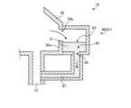
図6は、実施形態の変形例3に係る分析部60の構成の一例を示す図である。図6に示すように、変形例3に係る分析部60は、液受け部61の配置および構成が上記の実施形態と異なる。具体的には、変形例3では、液受け部61が回収カップ50よりも外側に、かつ回収カップ50と一体となって設けられる。
具体的には、回収カップ50の側壁50aに開口部50bが形成され、かかる開口部50bと液受け部61の流入口63とが繋がっている。また、回収カップ50の側壁50aの外側に、かかる側壁50aの一部を用いて液受け部61が形成される。
さらに、液受け部61の排出口64に排出流路67が接続され、かかる排出流路67は回収カップ50の排液口51に繋がっている。
このような構成であっても、液受け部61に滞留する処理液Sを濃度センサ62(図3参照)で測定することにより、ウェハWの枚葉処理に用いられた処理液Sに含まれる成分の濃度を精度よく検出することができる。
また、変形例3では、回収カップ50内に余剰スペースが無い処理ユニット16であっても、分析部60を問題無く設置することができる。
なお、この変形例3において、液受け部61などは、着脱可能に構成されていてもよい。またこの場合、液受け部61などを取り外す際には、回収カップ50に形成される開口部50bが蓋などで塞がれるとよい。
<変形例4>
図7は、実施形態の変形例4に係る処理ユニット16の具体的な構成の一例を示す模式図である。図7に示すように、変形例4では、分析部60の配置が上記の実施形態と異なる。具体的には、変形例4では、分析部60が回収カップ50の内部ではなく、回収カップ50の排液口51に接続される排出流路53に設けられる。
そして、変形例4では、回収カップ50によって捕集され、排液口51から排出流路53に流れ出た処理液S(図3参照)を、液受け部61(図3参照)で受ける。さらに、かかる液受け部61で受けた処理液Sに含まれる成分の濃度を、濃度センサ62(図3参照)で検出する。
このような構成であっても、制御部18(図1参照)は、ウェハWの枚葉処理に用いられた処理液Sに含まれる成分の濃度を精度よく検出することができる。
また、変形例4では、回収カップ50内に余剰スペースが無い処理ユニット16であっても、分析部60を問題無く設置することができる。
<変形例5>
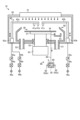
図8は、実施形態の変形例5に係る処理ユニット16の具体的な構成の一例を示す模式図である。図8に示すように、変形例5では、分析部60の配置および構成が上記の実施形態と異なる。
具体的には、変形例5では、分析部60の液受け部61が回収カップ50の内部ではなく、回収カップ50の排液口51に接続される排出流路53に設けられる。また、かかる液受け部61には、送液管68が接続される。
送液管68は、液受け部61とは異なる場所に設けられる被測定部69に繋がっており、液受け部61で受けた処理液Sを液受け部61から被測定部69に送液する。そして、分析部60は、被測定部69に送液された処理液Sに含まれる成分の濃度を、濃度センサ62で検出する。
このような構成であっても、制御部18(図1参照)は、ウェハWの枚葉処理に用いられた処理液Sに含まれる成分の濃度を精度よく検出することができる。
また、変形例5では、回収カップ50内に余剰スペースが無く、かつ排出流路53の周囲の余剰スペースが小さい処理ユニット16であっても、分析部60を問題無く設置することができる。
<変形例6>
図9は、実施形態の変形例6に係る処理ユニット16の具体的な構成の一例を示す模式図である。図9に示すように、変形例6では、液受け部61の配置が上記の変形例5と異なる。
具体的には、変形例6では、分析部60の液受け部61が排出流路53(図8参照)ではなく、回収カップ50の内部に設けられる。また、かかる液受け部61には、送液管68が接続される。
送液管68は、液受け部61とは異なる場所に設けられる被測定部69に繋がっており、液受け部61で受けた処理液Sを液受け部61から被測定部69に送液する。そして、分析部60は、被測定部69に送液された処理液Sに含まれる成分の濃度を、濃度センサ62で検出する。
このような構成であっても、制御部18(図1参照)は、ウェハWの枚葉処理に用いられた処理液Sに含まれる成分の濃度を精度よく検出することができる。
また、変形例6では、回収カップ50内の余剰スペースが小さい処理ユニット16であっても、分析部60を問題無く設置することができる。
<変形例7>
図10~図12は、実施形態の変形例7に係る処理ユニット16の具体的な構成および動作の一例を示す模式図である。図10に示すように、変形例7では、回収カップ50の構成が上記の実施形態と異なる。
具体的には、変形例7に係る回収カップ50は、第1回収カップ80と、第2回収カップ90と、第3回収カップ100とを有する。第1回収カップ80は、最も外側に設けられる回収カップであり、第3回収カップ100は、最も内側に設けられる回収カップであり、第2回収カップ90は、第1回収カップ80と第3回収カップ100との間に設けられる回収カップである。
第2回収カップ90は、昇降カップ91と、固定カップ92と、昇降ロッド93と、庇部94とを有する。昇降カップ91は、下部が円筒形状であり、上部が上方に進むにしたがい内側にすぼむ半円錐形状を有する。
固定カップ92は、昇降カップ91の下方に設けられる略円筒形状の部位である。かかる固定カップ92と昇降カップ91とで、回転するウェハWから飛散する処理液Sを受けるカップ体が形成される。また、昇降カップ91と固定カップ92とは、昇降カップ91が上昇した際にもカップ体が維持できるように、一部が重畳して配置される。
昇降ロッド93は、固定カップ92の内部に埋め込まれるように、昇降カップ91の下方に設けられる。昇降ロッド93は、たとえば磁力によって昇降カップ91と接続され、かかる昇降カップ91と一体的に昇降する。
庇部94は、固定カップ92に設けられ、かかる固定カップ92の内部で貫通するように形成される排気口52の開口部を上方から覆う。これにより、回収カップ50で回収される処理液Sが排気口52に流入することを抑制することができる。
第3回収カップ100は、昇降カップ101と、固定カップ102と、昇降ロッド103と、庇部104とを有する。昇降カップ101は、下部が円筒形状であり、上部が上方に進むにしたがい内側にすぼむ半円錐形状を有する。
固定カップ102は、昇降カップ101の下方に設けられる略円筒形状の部位である。かかる固定カップ102と昇降カップ101とで、回転するウェハWから飛散する処理液Sを受けるカップ体が形成される。また、昇降カップ101と固定カップ102とは、昇降カップ101が上昇した際にもカップ体が維持できるように、一部が重畳して配置される。
昇降ロッド103は、固定カップ102の内部に埋め込まれるように、昇降カップ101の下方に設けられる。昇降ロッド103は、たとえば磁力によって昇降カップ101と接続され、かかる昇降カップ101と一体的に昇降する。
庇部104は、固定カップ102に設けられ、かかる固定カップ102の内部で貫通するように形成される排気口52の開口部を上方から覆う。これにより、第3回収カップ100で回収される処理液Sが排気口52に流入することを抑制することができる。
図10の例では、ノズル41aからウェハWにDHFが供給される場合に、第2回収カップ90の昇降カップ91と、第3回収カップ100の昇降カップ101とが、いずれも所与の下降位置に配置される。
そのため、回転するウェハWから飛散する処理液Sは、第1回収カップ80と第2回収カップ90との間に形成される空間G1に流れ込む。そして、かかる空間G1の下流側に形成される排液口51Aから処理液Sが外部に排出される。
ここで、変形例7では、第1回収カップ80と第2回収カップ90との間に形成される空間G1に、分析部60Aが配置される。これにより、ノズル41aからウェハWにDHFが供給される液処理において、処理液Sに含まれる成分の濃度を検出することができる。
そして、変形例7では、回収カップ50を動作させることにより、処理液Sを排液口51Aとは異なる排液口に排出することができる。たとえば、図11に示すように、ノズル41cからウェハWにDIWが供給される場合に、制御部18(図1参照)は、昇降カップ91および昇降ロッド93を所与の上昇位置に移動させる。
これにより、回転するウェハWから飛散する処理液Sは、第2回収カップ90と第3回収カップ100との間に形成される空間G2に流れ込む。そして、かかる空間G2の下流側に形成される排液口51Bから処理液Sが外部に排出される。
ここで、変形例7では、第2回収カップ90と第3回収カップ100との間に形成される空間G2に、分析部60Bが配置される。これにより、ノズル41cからウェハWにDIWが供給される液処理において、処理液Sに含まれる成分の濃度を検出することができる。
さらに、変形例7では、図12に示すように、ノズル41bからウェハWにIPAが供給される場合に、制御部18(図1参照)が、昇降カップ91および昇降ロッド93に加えて、昇降カップ101および昇降ロッド103も所与の上昇位置に移動させる。
これにより、回転するウェハWから飛散する処理液Sは、第3回収カップ100とかかる第3回収カップ100の内側に位置する内壁部110との間に形成される空間G3に流れ込む。そして、かかる空間G3の下流側に形成される排液口51Cから処理液Sが外部に排出される。
ここで、変形例7では、第3回収カップ100と内壁部110との間に形成される空間G3に、分析部60Cが配置される。これにより、ノズル41bからウェハWにIPAが供給される液処理において、処理液Sに含まれる成分の濃度を検出することができる。
ここまで説明したように、変形例7では、処理ユニット16にウェハWから飛散する処理液Sを受ける回収カップが複数(ここでは、第1回収カップ80、第2回収カップ90および第3回収カップ100)設けられる。そして、分析部60は、これらの回収カップごとに複数設けられる。
これにより、複数種類の薬液ごとに回収カップが複数設けられる処理ユニット16において、すべての液処理で処理液Sに含まれる成分の濃度を検出することができる。
なお、図10~図12の例では、第1回収カップ80、第2回収カップ90および第3回収カップ100の内側にそれぞれ複数の分析部60(分析部60A、60B、60C)が設けられる例について示したが、本開示はかかる例に限られない。
たとえば、第1回収カップ80、第2回収カップ90および第3回収カップ100にそれぞれ接続される排液口51A、51B、51Cの下流側(すなわち、排出流路)に、それぞれ複数の分析部60(分析部60A、60B、60C)が設けられてもよい。
また、第1回収カップ80、第2回収カップ90および第3回収カップ100の内側にそれぞれ複数の液受け部61が設けられ、それぞれの液受け部61から別の場所に設けられる被測定部69に処理液Sが送液されてもよい(すなわち、図9の例と同様の構成)。
また、排液口51A、51B、51Cの下流側にそれぞれ複数の液受け部61が設けられ、それぞれの液受け部61から別の場所に設けられる被測定部69に処理液Sが送液されてもよい(すなわち、図8の例と同様の構成)。
また、図10~図12の例では、1つの処理ユニット16内に3つの回収カップ(第1回収カップ80、第2回収カップ90および第3回収カップ100)が設けられる例について示したが、本開示はかかる例に限られない。たとえば、1つの処理ユニット16内に2つの回収カップが設けられてもよいし、1つの処理ユニット16内に4つ以上の回収カップが設けられてもよい。
<変形例8>
図13は、実施形態の変形例8に係る処理ユニット16の具体的な構成の一例を示す模式図である。図13に示すように、変形例8では、上記の実施形態で説明した分析部60に加えて、ウェハW表面の処理液S(図3参照)の成分濃度を検出する別の濃度センサ62Aが設けられる。
かかる濃度センサ62Aは、投光部62a(図3参照)と受光部62b(図3参照)とが一体となっており、保持部31に保持されるウェハWの上方に配置される。かかる濃度センサ62Aは、たとえば、アーム42aまたはアーム42b(図ではアーム42b)に支持される。
そして、濃度センサ62Aは、シリコンで構成されるウェハWの表面で赤外光IRを反射させることにより、ウェハW表面の処理液Sの成分濃度を検出する。
ここで、変形例8では、制御部18(図1参照)が、分析部60に設けられる濃度センサ62(図3参照)による成分濃度の検出結果と、濃度センサ62Aによる成分濃度の検出結果とに基づいて、液処理の終点を判定するとよい。これにより、液処理の終点を精度よく判定することができる。
実施形態に係る基板処理装置(基板処理システム1)は、保持部31と、液供給部40と、分析部60と、を備える。保持部31は、基板(ウェハW)を保持して回転させる。液供給部40は、基板(ウェハW)に処理液Sを供給する。分析部60は、処理液Sを分析する。また、分析部60は、液受け部61と、濃度センサ62と、を有する。液受け部61は、基板(ウェハW)から流れ出る処理液Sを受ける。濃度センサ62は、液受け部61内に滞留する処理液Sに含まれる成分の濃度を検出する。これにより、ウェハWの枚葉処理に用いられた処理液Sに含まれる成分の濃度を精度よく検出することができる。
また、実施形態に係る基板処理装置(基板処理システム1)において、液受け部61は、流入口63と、排出口64と、被測定部65と、を有する。流入口63は、基板(ウェハW)から流れ出る処理液Sが流入する。排出口64は、流入口63よりも低い位置に配置され、内部に滞留する処理液Sを排出する。被測定部65は、流入口63よりも低く、かつ排出口64よりも高い位置に配置され、濃度センサ62によって処理液Sが測定される。これにより、ウェハWの枚葉処理において、かかるウェハWから流れ出る処理液Sの成分濃度の時間経過を連続的に検出することができる。
また、実施形態に係る基板処理装置(基板処理システム1)において、基板(ウェハW)の液処理時において被測定部65に処理液Sが常時滞留するように、流入口63および排出口64の大きさが設定される。これにより、ウェハWの液処理の最初から最後まで、処理液Sの成分濃度の時間経過を連続的に検出することができる。
また、実施形態に係る基板処理装置(基板処理システム1)において、排出口64は、液受け部61に複数設けられる。これにより、ウェハWの枚葉処理において、かかるウェハWから流れ出る処理液Sの成分濃度の時間経過を円滑に検出することができる。
また、実施形態に係る基板処理装置(基板処理システム1)は、基板(ウェハW)から飛散する処理液Sを受ける回収カップ50、を備える。また、液受け部61は、回収カップ50の外側に設けられる。これにより、回収カップ50内に余剰スペースが無い処理ユニット16であっても、分析部60を問題無く設置することができる。
また、実施形態に係る基板処理装置(基板処理システム1)は、保持部31と、液供給部40と、分析部60と、を備える。保持部31は、基板(ウェハW)を保持して回転させる。液供給部40は、基板(ウェハW)に処理液Sを供給する。分析部60は、処理液Sを分析する。また、分析部60は、液受け部61と、送液管68と、濃度センサ62と、を有する。液受け部61は、基板(ウェハW)から流れ出る処理液Sを受ける。送液管68は、液受け部61から被測定部69まで処理液Sを送液する。濃度センサ62は、被測定部69において処理液Sに含まれる成分の濃度を検出する。これにより、ウェハWの枚葉処理に用いられた処理液Sに含まれる成分の濃度を精度よく検出することができる。
また、実施形態に係る基板処理装置(基板処理システム1)は、基板(ウェハW)から飛散する処理液Sを受ける回収カップ50、を備える。また、液受け部61は、回収カップ50内に設けられる。これにより、ウェハWの枚葉処理に用いられた処理液Sに含まれる成分の濃度を精度よく検出することができる。
また、実施形態に係る基板処理装置(基板処理システム1)は、基板(ウェハW)から飛散する処理液Sを受ける回収カップ50と、回収カップ50から処理液Sを排出する排出流路53と、を備える。また、液受け部61は、排出流路53に設けられる。これにより、回収カップ50内に余剰スペースが無い処理ユニット16であっても、分析部60を問題無く設置することができる。
また、実施形態に係る基板処理装置(基板処理システム1)は、基板(ウェハW)から飛散する処理液Sを受ける回収カップを複数(第1回収カップ80、第2回収カップ90および第3回収カップ100)備える。また、液受け部61は、回収カップ(第1回収カップ80、第2回収カップ90および第3回収カップ100)ごとに複数設けられる。これにより、複数種類の薬液ごとに回収カップが複数設けられる処理ユニット16において、すべての液処理で処理液Sに含まれる成分の濃度を検出することができる。
また、実施形態に係る基板処理装置(基板処理システム1)において、濃度センサ62は、赤外分光法によって成分の濃度を検出する。これにより、ウェハWから流れ出る処理液Sに含まれる成分の濃度を精度よくかつ簡便に検出することができる。
また、実施形態に係る基板処理装置(基板処理システム1)において、濃度センサ62は、導電率計によって成分の濃度を検出する。これにより、ウェハWから流れ出る処理液Sに含まれる成分の濃度を精度よく検出することができる。
また、実施形態に係る基板処理方法は、上記の基板処理装置(基板処理システム1)において、基板(ウェハW)上の処理液を異なる処理液に置換する処理において、処理の設定時間を濃度センサ62の測定値に基づいて決定する決定処理、を含む。これにより、液処理のランニングコストを低減することができる。
また、実施形態に係る基板処理方法は、上記の基板処理装置(基板処理システム1)において、判定処理と、報知処理とを含む。判定処理は、濃度センサ62の測定値に基づいて、液処理が正常に完了しているか否かを判定する。報知処理は、液処理が正常に完了していない場合に、外部にアラームを出力する。これにより、ウェハWの液処理を安定して実施することができる。
また、実施形態に係る基板処理方法において、液処理が正常に完了していない場合に、かかる液処理の対象であった基板(ウェハW)をレスキューレシピによって救出する救出処理をさらに含む。これにより、ウェハWの歩留まりを向上させることができる。
以上、本開示の実施形態について説明したが、本開示は上記実施形態に限定されるものではなく、その趣旨を逸脱しない限りにおいて種々の変更が可能である。
今回開示された実施形態は全ての点で例示であって制限的なものではないと考えられるべきである。実に、上記した実施形態は多様な形態で具現され得る。また、上記の実施形態は、添付の請求の範囲及びその趣旨を逸脱することなく、様々な形態で省略、置換、変更されてもよい。