JP7586899B2 - マイクロ流体デバイスのための導電性スペーサ - Google Patents
マイクロ流体デバイスのための導電性スペーサ Download PDFInfo
- Publication number
- JP7586899B2 JP7586899B2 JP2022517835A JP2022517835A JP7586899B2 JP 7586899 B2 JP7586899 B2 JP 7586899B2 JP 2022517835 A JP2022517835 A JP 2022517835A JP 2022517835 A JP2022517835 A JP 2022517835A JP 7586899 B2 JP7586899 B2 JP 7586899B2
- Authority
- JP
- Japan
- Prior art keywords
- gasket
- substrate
- conductive
- fluid chamber
- edge
- Prior art date
- Legal status (The legal status is an assumption and is not a legal conclusion. Google has not performed a legal analysis and makes no representation as to the accuracy of the status listed.)
- Active
Links
Images


















Classifications
-
- B—PERFORMING OPERATIONS; TRANSPORTING
- B01—PHYSICAL OR CHEMICAL PROCESSES OR APPARATUS IN GENERAL
- B01L—CHEMICAL OR PHYSICAL LABORATORY APPARATUS FOR GENERAL USE
- B01L3/00—Containers or dishes for laboratory use, e.g. laboratory glassware; Droppers
- B01L3/50—Containers for the purpose of retaining a material to be analysed, e.g. test tubes
- B01L3/502—Containers for the purpose of retaining a material to be analysed, e.g. test tubes with fluid transport, e.g. in multi-compartment structures
- B01L3/5027—Containers for the purpose of retaining a material to be analysed, e.g. test tubes with fluid transport, e.g. in multi-compartment structures by integrated microfluidic structures, i.e. dimensions of channels and chambers are such that surface tension forces are important, e.g. lab-on-a-chip
- B01L3/502769—Containers for the purpose of retaining a material to be analysed, e.g. test tubes with fluid transport, e.g. in multi-compartment structures by integrated microfluidic structures, i.e. dimensions of channels and chambers are such that surface tension forces are important, e.g. lab-on-a-chip characterised by multiphase flow arrangements
- B01L3/502784—Containers for the purpose of retaining a material to be analysed, e.g. test tubes with fluid transport, e.g. in multi-compartment structures by integrated microfluidic structures, i.e. dimensions of channels and chambers are such that surface tension forces are important, e.g. lab-on-a-chip characterised by multiphase flow arrangements specially adapted for droplet or plug flow, e.g. digital microfluidics
-
- B—PERFORMING OPERATIONS; TRANSPORTING
- B01—PHYSICAL OR CHEMICAL PROCESSES OR APPARATUS IN GENERAL
- B01L—CHEMICAL OR PHYSICAL LABORATORY APPARATUS FOR GENERAL USE
- B01L3/00—Containers or dishes for laboratory use, e.g. laboratory glassware; Droppers
- B01L3/50—Containers for the purpose of retaining a material to be analysed, e.g. test tubes
- B01L3/502—Containers for the purpose of retaining a material to be analysed, e.g. test tubes with fluid transport, e.g. in multi-compartment structures
- B01L3/5027—Containers for the purpose of retaining a material to be analysed, e.g. test tubes with fluid transport, e.g. in multi-compartment structures by integrated microfluidic structures, i.e. dimensions of channels and chambers are such that surface tension forces are important, e.g. lab-on-a-chip
- B01L3/50273—Containers for the purpose of retaining a material to be analysed, e.g. test tubes with fluid transport, e.g. in multi-compartment structures by integrated microfluidic structures, i.e. dimensions of channels and chambers are such that surface tension forces are important, e.g. lab-on-a-chip characterised by the means or forces applied to move the fluids
-
- B—PERFORMING OPERATIONS; TRANSPORTING
- B01—PHYSICAL OR CHEMICAL PROCESSES OR APPARATUS IN GENERAL
- B01L—CHEMICAL OR PHYSICAL LABORATORY APPARATUS FOR GENERAL USE
- B01L2200/00—Solutions for specific problems relating to chemical or physical laboratory apparatus
- B01L2200/02—Adapting objects or devices to another
- B01L2200/026—Fluid interfacing between devices or objects, e.g. connectors, inlet details
-
- B—PERFORMING OPERATIONS; TRANSPORTING
- B01—PHYSICAL OR CHEMICAL PROCESSES OR APPARATUS IN GENERAL
- B01L—CHEMICAL OR PHYSICAL LABORATORY APPARATUS FOR GENERAL USE
- B01L2200/00—Solutions for specific problems relating to chemical or physical laboratory apparatus
- B01L2200/06—Fluid handling related problems
- B01L2200/0673—Handling of plugs of fluid surrounded by immiscible fluid
-
- B—PERFORMING OPERATIONS; TRANSPORTING
- B01—PHYSICAL OR CHEMICAL PROCESSES OR APPARATUS IN GENERAL
- B01L—CHEMICAL OR PHYSICAL LABORATORY APPARATUS FOR GENERAL USE
- B01L2200/00—Solutions for specific problems relating to chemical or physical laboratory apparatus
- B01L2200/06—Fluid handling related problems
- B01L2200/0689—Sealing
-
- B—PERFORMING OPERATIONS; TRANSPORTING
- B01—PHYSICAL OR CHEMICAL PROCESSES OR APPARATUS IN GENERAL
- B01L—CHEMICAL OR PHYSICAL LABORATORY APPARATUS FOR GENERAL USE
- B01L2200/00—Solutions for specific problems relating to chemical or physical laboratory apparatus
- B01L2200/12—Specific details about manufacturing devices
-
- B—PERFORMING OPERATIONS; TRANSPORTING
- B01—PHYSICAL OR CHEMICAL PROCESSES OR APPARATUS IN GENERAL
- B01L—CHEMICAL OR PHYSICAL LABORATORY APPARATUS FOR GENERAL USE
- B01L2300/00—Additional constructional details
- B01L2300/06—Auxiliary integrated devices, integrated components
- B01L2300/0627—Sensor or part of a sensor is integrated
- B01L2300/0645—Electrodes
-
- B—PERFORMING OPERATIONS; TRANSPORTING
- B01—PHYSICAL OR CHEMICAL PROCESSES OR APPARATUS IN GENERAL
- B01L—CHEMICAL OR PHYSICAL LABORATORY APPARATUS FOR GENERAL USE
- B01L2300/00—Additional constructional details
- B01L2300/08—Geometry, shape and general structure
- B01L2300/0809—Geometry, shape and general structure rectangular shaped
- B01L2300/0816—Cards, e.g. flat sample carriers usually with flow in two horizontal directions
-
- B—PERFORMING OPERATIONS; TRANSPORTING
- B01—PHYSICAL OR CHEMICAL PROCESSES OR APPARATUS IN GENERAL
- B01L—CHEMICAL OR PHYSICAL LABORATORY APPARATUS FOR GENERAL USE
- B01L2300/00—Additional constructional details
- B01L2300/08—Geometry, shape and general structure
- B01L2300/0861—Configuration of multiple channels and/or chambers in a single devices
-
- B—PERFORMING OPERATIONS; TRANSPORTING
- B01—PHYSICAL OR CHEMICAL PROCESSES OR APPARATUS IN GENERAL
- B01L—CHEMICAL OR PHYSICAL LABORATORY APPARATUS FOR GENERAL USE
- B01L2300/00—Additional constructional details
- B01L2300/08—Geometry, shape and general structure
- B01L2300/089—Virtual walls for guiding liquids
-
- B—PERFORMING OPERATIONS; TRANSPORTING
- B01—PHYSICAL OR CHEMICAL PROCESSES OR APPARATUS IN GENERAL
- B01L—CHEMICAL OR PHYSICAL LABORATORY APPARATUS FOR GENERAL USE
- B01L2400/00—Moving or stopping fluids
- B01L2400/04—Moving fluids with specific forces or mechanical means
- B01L2400/0403—Moving fluids with specific forces or mechanical means specific forces
- B01L2400/0415—Moving fluids with specific forces or mechanical means specific forces electrical forces, e.g. electrokinetic
- B01L2400/0427—Electrowetting
Landscapes
- Chemical & Material Sciences (AREA)
- Health & Medical Sciences (AREA)
- Dispersion Chemistry (AREA)
- Analytical Chemistry (AREA)
- General Health & Medical Sciences (AREA)
- Hematology (AREA)
- Clinical Laboratory Science (AREA)
- Chemical Kinetics & Catalysis (AREA)
- Physical Or Chemical Processes And Apparatus (AREA)
- Sampling And Sample Adjustment (AREA)
Description
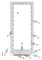
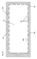
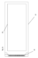
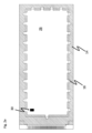
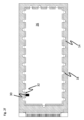
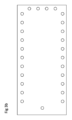
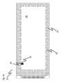
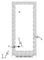
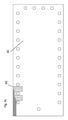
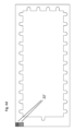
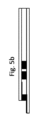
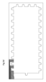
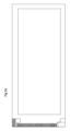
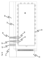
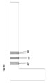
図2aは、本発明の一態様による例示的なAMEWODデバイス(10)の上からの平面図を示し、液体試料は、上部基板のエッジに沿ってデバイスに導入される。AMEWODデバイス(10)は、下部基板(12)、ガスケット(14)、上部基板(16)、ポート(18、28)、エッジコネクタ(20)およびコンタクトパッド(22)を備える。明確にするために、図2bはガスケット(14)および上部基板(16)のみを示し、図2cは下部基板のみを示す。図2cの線23は、デバイスのアクティブ領域の境界を示す。
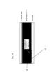
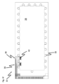
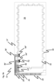
図2e-図2gは、図2aのAM-EWODデバイスを示しており、予めポート(28)を介してオイルで少なくとも部分的に充填された流体チャンバ内26に、AMEWODデバイス(10)のポート(18または類似のもの)を通して液体試料(30)を導入した後の図である。液体試料(30)は、例えば、ピペットまたはシリンジ(図示せず)を使用して、ポート(18)を通して導入することができる。最初に(図2e)、ポート(18)を通して液体試料(30)を適用した後、液体試料(30)は、エレクトロウェッティングによってキャビティ(26)内に移送され得る。マイクロプロセッサ(図示せず)は、スクリプトを用いて、エレクトロウェッティングによって極性液体の試料の移動を制御するように設計されたプロトコルを動作させるように構成され得る。
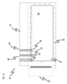
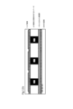
それぞれの各電極対(36、38)は、i)液滴の電流測定または電位差測定などの電気化学測定を行うこと、ii)液滴にチャージ電圧を印加すること、iii)液滴のインピーダンス特性を決定すること、を含む、様々な目的のために使用されることができるが、これらに限定されない。図4fは、電極対(36、38)のそれぞれの各電極における液滴(42)の存在を示す。各液滴(42)の特性は、適切な測定プロセスによって適宜に決定されてもよいし、または、チャージ電圧がそのような液滴に印加されてもよい。
以下に、本願出願当初の特許請求の範囲に記載された発明を付記する。
[1] マイクロ流体デバイスであって、
第1基板および第2基板と、
前記第1基板と前記第2基板との間に流体チャンバを画定するために、前記第1基板を前記第2基板から離間するガスケットであって、前記ガスケットの内側エッジ面が前記流体チャンバの側面境界を画定する、ガスケットと、
前記流体チャンバに面する前記第1基板の表面上に設けられた複数の独立してアドレス指定可能なアレイ素子と、
前記流体チャンバに面する前記第2基板の表面上に配置された少なくとも1つの回路素子と、
流体試料を前記流体チャンバに導入するための少なくとも1つのポートと、を備え、
前記ガスケットは、前記流体チャンバに面する前記第2基板の表面上に配置された回路素子と、関連する端子との間に導電性経路を提供するように構成される、
マイクロ流体デバイス。
[2] 前記端子が、前記第1基板上に設けられ、前記ガスケットが、少なくとも前記ガスケットの厚さ方向に延在する前記導電性経路を提供する、[1]に記載のデバイス。
[3] 前記ガスケットは、前記ガスケットの平面内にさらに延在する前記導電性経路を提供する、[2]に記載のデバイス。
[4] 前記端子は、前記ガスケットの前記内側エッジ面から離れた位置で、前記ガスケット上に設けられ、前記ガスケットは、少なくとも前記ガスケットの平面内に延在する導電性経路を提供する、[1]に記載のデバイス。
[5] 前記ガスケットは、バルクで電気的に導電性である、[1]~[4]のいずれか一項に記載のデバイス。
[6] 複数の回路要素が、前記流体チャンバに面する前記第2基板の前記表面上に設けられ、前記ガスケットが、複数の独立した導電性経路を提供するように構成され、各導電性経路は、前記回路要素のそれぞれの1つと、それぞれの関連する端子との間にある、[1]~[4]のいずれか一項に記載のデバイス。
[7] 前記ガスケットは、前記第1基板および前記第2基板を越えて突出する突出部分を備え、前記導電性経路は、前記ガスケットの前記突出部分まで延在する、[6]に記載のデバイス。
[8] 電気的導電層が、前記流体チャンバ層に面する前記第2基板の前記表面上に設けられ、前記回路素子が前記電気的導電層内に画定される、[6]または[7]に記載のデバイス。
[9] 前記ガスケットが、前記ガスケットの前記内側エッジ面の一部に配置された導電性部材と、関連する端子との間に導電性経路をさらに提供する、[6]、[7]、または[8]のいずれか一項に記載のデバイス。
[10] 前記ガスケットは、異方性電気的導電率を有する材料を備え、および、任意選択で、前記ガスケットが、前記ガスケットの厚さ方向に電気的に導電性であり、前記厚さ方向と垂直な方向に実質的に導電性でない材料を備える、[6]、[7]、または[8]のいずれか一項に記載のデバイス。
[11] 前記ガスケットの前記内側エッジ面は、前記少なくとも1つのポートを画定するように成形される、[1]~[10]のいずれか一項に記載のデバイス。
[12] [1]~[11]のいずれか一項に記載のデバイスの前記流体チャンバに流体試料を導入することと
前記流体試料を、前記第2基板上に配置された前記回路素子または前記回路素子のうちの選択された1つに隣接するように移動するために、前記デバイスの前記第1基板上に設けられた前記アレイ素子を制御することと、
前記回路素子または前記選択された回路素子に関連付けられた前記端子に電圧を印加すること、
を備える、方法。
[13] 前記流体試料をチャージするために、前記電圧を印加することを備える、[12]に記載の方法。
[14] 1つまたは複数のさらなる流体操作を前記チャージされた流体試料に行うことを備え、任意選択で、前記1つまたは複数のさらなる流体操作を前記チャージされた流体試料に行うことは、少なくとも1つの流体液滴を前記流体試料から分離することを備える、[13]に記載の方法。
[15] 測定信号を前記流体試料に通すために、前記電圧を印加することを備える、[12]に記載の方法。
Claims (15)
- マイクロ流体デバイスであって、
第1基板および第2基板と、
前記第1基板と前記第2基板との間に流体チャンバを画定するために、前記第1基板を前記第2基板から離間するガスケットであって、前記ガスケットの内側エッジ面が前記流体チャンバの側面境界を画定する、ガスケットと、
前記流体チャンバに面する前記第1基板の表面上に設けられた複数の独立してアドレス指定可能なアレイ素子と、
前記流体チャンバに面する前記第2基板の表面上に配置された少なくとも1つの回路素子と、
流体試料を前記流体チャンバに導入するための少なくとも1つのポートと、を備え、
前記ガスケットは、1つの方向にのみ、または1つの方向に少なくとも優先的に導電性を有するスペーサとしても機能し、前記流体チャンバに面する前記第2基板の表面上に配置された回路素子と、関連する端子との間に導電性経路を提供するように構成される、
マイクロ流体デバイス。 - 前記端子が、前記第1基板上に設けられ、前記ガスケットが、少なくとも前記ガスケットの厚さ方向に延在する前記導電性経路を提供する、請求項1に記載のデバイス。
- 前記ガスケットは、前記ガスケットの平面内にさらに延在する前記導電性経路を提供する、請求項2に記載のデバイス。
- 前記端子は、前記ガスケットの前記内側エッジ面から離れた位置で、前記ガスケット上に設けられ、前記ガスケットは、少なくとも前記ガスケットの平面内に延在する導電性経路を提供する、請求項1に記載のデバイス。
- 前記ガスケットは、異方性導電性材料のバルクで形成される、請求項1~4のいずれか一項に記載のデバイス。
- 複数の回路要素が、前記流体チャンバに面する前記第2基板の前記表面上に設けられ、前記ガスケットが、複数の独立した導電性経路を提供するように構成され、各導電性経路は、前記回路要素のそれぞれの1つと、それぞれの関連する端子との間にある、請求項1~4のいずれか一項に記載のデバイス。
- 前記ガスケットは、前記第1基板および前記第2基板を越えて突出する突出部分を備え、前記導電性経路は、前記ガスケットの前記突出部分まで延在する、請求項6に記載のデバイス。
- 電気的導電層が、前記流体チャンバ層に面する前記第2基板の前記表面上に設けられ、前記回路素子が前記電気的導電層内に画定される、請求項6または7に記載のデバイス。
- 前記ガスケットが、前記ガスケットの前記内側エッジ面の一部に配置された導電性部材と、関連する端子との間に導電性経路をさらに提供する、請求項6、7、または8のいずれか一項に記載のデバイス。
- 前記ガスケットが、前記ガスケットの厚さ方向に電気的に導電性であり、前記厚さ方向と垂直な方向に実質的に導電性でない材料を備える、請求項6、7、または8のいずれか一項に記載のデバイス。
- 前記ガスケットの前記内側エッジ面は、前記少なくとも1つのポートを画定するように成形される、請求項1~10のいずれか一項に記載のデバイス。
- 請求項1~11のいずれか一項に記載のデバイスの前記流体チャンバに流体試料を導入することと、
前記流体試料を、前記第2基板上に配置された前記回路素子または前記回路素子のうちの選択された1つに隣接するように移動するために、前記デバイスの前記第1基板上に設けられた前記アレイ素子を制御することと、
前記回路素子または前記選択された回路素子に関連付けられた前記端子に電圧を印加すること、
を備える、方法。 - 前記流体試料をチャージするために、前記電圧を印加することを備える、請求項12に記載の方法。
- 1つまたは複数のさらなる流体操作を前記チャージされた流体試料に行うことを備え、任意選択で、前記1つまたは複数のさらなる流体操作を前記チャージされた流体試料に行うことは、少なくとも1つの流体液滴を前記流体試料から分離することを備える、請求項13に記載の方法。
- 測定信号を前記流体試料に通すために、前記電圧を印加することを備える、請求項12に記載の方法。
Priority Applications (1)
| Application Number | Priority Date | Filing Date | Title |
|---|---|---|---|
| JP2024106200A JP7757470B2 (ja) | 2019-09-19 | 2024-07-01 | マイクロ流体デバイスのための導電性スペーサ |
Applications Claiming Priority (3)
| Application Number | Priority Date | Filing Date | Title |
|---|---|---|---|
| EP19198483.0A EP3795252B1 (en) | 2019-09-19 | 2019-09-19 | Conductive spacer for a microfluidic device |
| EP19198483.0 | 2019-09-19 | ||
| PCT/EP2020/076189 WO2021053196A1 (en) | 2019-09-19 | 2020-09-18 | Conductive spacer for a microfluidic device |
Related Child Applications (1)
| Application Number | Title | Priority Date | Filing Date |
|---|---|---|---|
| JP2024106200A Division JP7757470B2 (ja) | 2019-09-19 | 2024-07-01 | マイクロ流体デバイスのための導電性スペーサ |
Publications (2)
| Publication Number | Publication Date |
|---|---|
| JP2022549205A JP2022549205A (ja) | 2022-11-24 |
| JP7586899B2 true JP7586899B2 (ja) | 2024-11-19 |
Family
ID=67998220
Family Applications (2)
| Application Number | Title | Priority Date | Filing Date |
|---|---|---|---|
| JP2022517835A Active JP7586899B2 (ja) | 2019-09-19 | 2020-09-18 | マイクロ流体デバイスのための導電性スペーサ |
| JP2024106200A Active JP7757470B2 (ja) | 2019-09-19 | 2024-07-01 | マイクロ流体デバイスのための導電性スペーサ |
Family Applications After (1)
| Application Number | Title | Priority Date | Filing Date |
|---|---|---|---|
| JP2024106200A Active JP7757470B2 (ja) | 2019-09-19 | 2024-07-01 | マイクロ流体デバイスのための導電性スペーサ |
Country Status (6)
| Country | Link |
|---|---|
| US (1) | US20220355299A1 (ja) |
| EP (1) | EP3795252B1 (ja) |
| JP (2) | JP7586899B2 (ja) |
| KR (1) | KR102839037B1 (ja) |
| CN (1) | CN114793427B (ja) |
| WO (1) | WO2021053196A1 (ja) |
Citations (5)
| Publication number | Priority date | Publication date | Assignee | Title |
|---|---|---|---|---|
| JP2007132749A (ja) | 2005-11-09 | 2007-05-31 | Hitachi Ltd | 液体搬送装置 |
| JP2013142753A (ja) | 2012-01-10 | 2013-07-22 | Sekisui Chem Co Ltd | エレクトロウェッティングディスプレイ |
| JP2015108848A (ja) | 2010-02-02 | 2015-06-11 | ピクストロニックス・インコーポレーテッド | 低温封孔流体充填ディスプレイ装置を製造するための方法 |
| JP2018171612A (ja) | 2017-03-31 | 2018-11-08 | シャープ ライフ サイエンス (イーユー) リミテッド | 断続的な駆動パターンを有するam‐ewod装置及び制御方法 |
| JP2019018197A (ja) | 2017-07-12 | 2019-02-07 | シャープ ライフ サイエンス (イーユー) リミテッド | サイドロードされるewodデバイスのためのスペーサ |
Family Cites Families (20)
| Publication number | Priority date | Publication date | Assignee | Title |
|---|---|---|---|---|
| WO2003068403A1 (en) * | 2002-02-12 | 2003-08-21 | Femtodrop Corporation | Device to print biofluids |
| US20050098750A1 (en) * | 2003-11-06 | 2005-05-12 | Daniel Sobek | Electrostatic sealing device and method of use thereof |
| CN101405084B (zh) * | 2006-03-20 | 2011-11-16 | 皇家飞利浦电子股份有限公司 | 用于电子微流体设备的系统级封装台 |
| US9176318B2 (en) * | 2007-05-18 | 2015-11-03 | Pixtronix, Inc. | Methods for manufacturing fluid-filled MEMS displays |
| US7906735B2 (en) * | 2007-07-05 | 2011-03-15 | Raytheon Company | Electrically conductive dynamic environmental seal |
| US9005544B2 (en) * | 2009-10-15 | 2015-04-14 | The Regents Of The University Of California | Digital microfluidic platform for radiochemistry |
| EP2522042A2 (en) * | 2010-01-08 | 2012-11-14 | Koninklijke Philips Electronics N.V. | Method of maskless manufacturing of oled devices |
| US8685325B2 (en) * | 2010-03-09 | 2014-04-01 | Sparkle Power Inc. | Field-programmable lab-on-a-chip based on microelectrode array architecture |
| US20130062205A1 (en) * | 2011-09-14 | 2013-03-14 | Sharp Kabushiki Kaisha | Active matrix device for fluid control by electro-wetting and dielectrophoresis and method of driving |
| KR101911087B1 (ko) | 2011-11-22 | 2018-12-31 | 리쿠아비스타 비.브이. | 전기 습윤 표시 패널의 구동 방법 및 이를 수행하는 전기 습윤 표시 장치 |
| US8821705B2 (en) * | 2011-11-25 | 2014-09-02 | Tecan Trading Ag | Digital microfluidics system with disposable cartridges |
| TWI477851B (zh) * | 2012-05-22 | 2015-03-21 | Au Optronics Corp | 觸控顯示面板與觸控液晶顯示面板 |
| US9119285B2 (en) * | 2012-06-19 | 2015-08-25 | Apple Inc. | Conductive gaskets with internal cavities |
| KR101957998B1 (ko) * | 2012-06-20 | 2019-07-03 | 삼성디스플레이 주식회사 | 표시 패널 및 이의 제조 방법 |
| WO2014153335A1 (en) * | 2013-03-20 | 2014-09-25 | Molex Incorporated | Shielding cage for closely spaced cage arrays |
| US20150310787A1 (en) * | 2013-10-21 | 2015-10-29 | Pixtronix, Inc. | Ems displays incorporating conductive edge seals and methods for manufacturing thereof |
| US9841402B2 (en) * | 2015-04-15 | 2017-12-12 | Sharp Life Science (Eu) Limited | Multifunction electrode with combined heating and EWOD drive functionality |
| KR101891401B1 (ko) * | 2016-08-12 | 2018-08-23 | 고려대학교 산학협력단 | 미세유체 소자 및 이의 제조방법 |
| EP3357578B1 (en) * | 2017-02-06 | 2021-01-06 | Sharp Life Science (EU) Limited | Temperature control system for microfluidic device |
| US20190329258A1 (en) * | 2018-04-25 | 2019-10-31 | Tecan Trading Ag | Cartridge and electrowetting sample processing system with delivery zone |
-
2019
- 2019-09-19 EP EP19198483.0A patent/EP3795252B1/en active Active
-
2020
- 2020-09-18 US US17/641,631 patent/US20220355299A1/en active Pending
- 2020-09-18 CN CN202080065584.4A patent/CN114793427B/zh active Active
- 2020-09-18 KR KR1020227012710A patent/KR102839037B1/ko active Active
- 2020-09-18 JP JP2022517835A patent/JP7586899B2/ja active Active
- 2020-09-18 WO PCT/EP2020/076189 patent/WO2021053196A1/en not_active Ceased
-
2024
- 2024-07-01 JP JP2024106200A patent/JP7757470B2/ja active Active
Patent Citations (5)
| Publication number | Priority date | Publication date | Assignee | Title |
|---|---|---|---|---|
| JP2007132749A (ja) | 2005-11-09 | 2007-05-31 | Hitachi Ltd | 液体搬送装置 |
| JP2015108848A (ja) | 2010-02-02 | 2015-06-11 | ピクストロニックス・インコーポレーテッド | 低温封孔流体充填ディスプレイ装置を製造するための方法 |
| JP2013142753A (ja) | 2012-01-10 | 2013-07-22 | Sekisui Chem Co Ltd | エレクトロウェッティングディスプレイ |
| JP2018171612A (ja) | 2017-03-31 | 2018-11-08 | シャープ ライフ サイエンス (イーユー) リミテッド | 断続的な駆動パターンを有するam‐ewod装置及び制御方法 |
| JP2019018197A (ja) | 2017-07-12 | 2019-02-07 | シャープ ライフ サイエンス (イーユー) リミテッド | サイドロードされるewodデバイスのためのスペーサ |
Also Published As
| Publication number | Publication date |
|---|---|
| JP2024156663A (ja) | 2024-11-06 |
| EP3795252A1 (en) | 2021-03-24 |
| CN114793427B (zh) | 2024-04-16 |
| KR102839037B1 (ko) | 2025-07-25 |
| JP7757470B2 (ja) | 2025-10-21 |
| CN114793427A (zh) | 2022-07-26 |
| WO2021053196A1 (en) | 2021-03-25 |
| US20220355299A1 (en) | 2022-11-10 |
| JP2022549205A (ja) | 2022-11-24 |
| EP3795252B1 (en) | 2025-12-24 |
| KR20220083706A (ko) | 2022-06-20 |
Similar Documents
| Publication | Publication Date | Title |
|---|---|---|
| US11169109B2 (en) | Electrochemical detection chip and detection method thereof | |
| CN107754962B (zh) | 一种数字微流控液滴驱动装置及驱动方法 | |
| US10183292B2 (en) | Capacitance detection in a droplet actuator | |
| US7641779B2 (en) | Method and apparatus for programmable fluidic processing | |
| US20100126860A1 (en) | PCB Droplet Actuator Fabrication | |
| BRPI0607213B1 (pt) | aparelho para manipulação de gotículas em uma placa de circuito impresso | |
| US20210008549A1 (en) | Low sample volume sensing device | |
| US10365533B2 (en) | Electrophoretic display device and electronic apparatus | |
| CN115605748A (zh) | 包括场效应晶体管生物传感器的数字微流控装置及场效应检测的方法 | |
| US20220091146A1 (en) | Devices and methods for fluid actuation | |
| JP7586899B2 (ja) | マイクロ流体デバイスのための導電性スペーサ | |
| CN114585441B (zh) | 微流控芯片、文库制备芯片、液滴控制驱动方法 | |
| JP6678229B2 (ja) | 生体試料分析チップ、生体試料分析装置、及び生体試料分析方法 | |
| US20080211883A1 (en) | Liquid discharge apparatus and check method of the same | |
| US20140125897A1 (en) | Electric device having variable capacitance element and its manufacture | |
| JP7744821B2 (ja) | 流路デバイス | |
| CN117019242A (zh) | 一种集成温度传感器的微流控芯片封装结构及封装方法 | |
| US9120098B2 (en) | Fluid handling device and fluid handling system | |
| CN114981010A (zh) | 用于液滴驱动的基板及其制造方法、微流控装置 | |
| US20240402224A1 (en) | Ewod device with sensing apparatus | |
| JP6310327B2 (ja) | 流体取扱装置 |
Legal Events
| Date | Code | Title | Description |
|---|---|---|---|
| A621 | Written request for application examination |
Free format text: JAPANESE INTERMEDIATE CODE: A621 Effective date: 20230821 |
|
| RD02 | Notification of acceptance of power of attorney |
Free format text: JAPANESE INTERMEDIATE CODE: A7422 Effective date: 20230821 |
|
| A977 | Report on retrieval |
Free format text: JAPANESE INTERMEDIATE CODE: A971007 Effective date: 20240326 |
|
| A131 | Notification of reasons for refusal |
Free format text: JAPANESE INTERMEDIATE CODE: A131 Effective date: 20240402 |
|
| A521 | Request for written amendment filed |
Free format text: JAPANESE INTERMEDIATE CODE: A523 Effective date: 20240701 |
|
| TRDD | Decision of grant or rejection written | ||
| A01 | Written decision to grant a patent or to grant a registration (utility model) |
Free format text: JAPANESE INTERMEDIATE CODE: A01 Effective date: 20241008 |
|
| A61 | First payment of annual fees (during grant procedure) |
Free format text: JAPANESE INTERMEDIATE CODE: A61 Effective date: 20241107 |
|
| R150 | Certificate of patent or registration of utility model |
Ref document number: 7586899 Country of ref document: JP Free format text: JAPANESE INTERMEDIATE CODE: R150 |