JP7586899B2 - Conductive spacers for microfluidic devices - Google Patents
Conductive spacers for microfluidic devices Download PDFInfo
- Publication number
- JP7586899B2 JP7586899B2 JP2022517835A JP2022517835A JP7586899B2 JP 7586899 B2 JP7586899 B2 JP 7586899B2 JP 2022517835 A JP2022517835 A JP 2022517835A JP 2022517835 A JP2022517835 A JP 2022517835A JP 7586899 B2 JP7586899 B2 JP 7586899B2
- Authority
- JP
- Japan
- Prior art keywords
- gasket
- substrate
- conductive
- fluid chamber
- edge
- Prior art date
- Legal status (The legal status is an assumption and is not a legal conclusion. Google has not performed a legal analysis and makes no representation as to the accuracy of the status listed.)
- Active
Links
Images


















Classifications
-
- B—PERFORMING OPERATIONS; TRANSPORTING
- B01—PHYSICAL OR CHEMICAL PROCESSES OR APPARATUS IN GENERAL
- B01L—CHEMICAL OR PHYSICAL LABORATORY APPARATUS FOR GENERAL USE
- B01L3/00—Containers or dishes for laboratory use, e.g. laboratory glassware; Droppers
- B01L3/50—Containers for the purpose of retaining a material to be analysed, e.g. test tubes
- B01L3/502—Containers for the purpose of retaining a material to be analysed, e.g. test tubes with fluid transport, e.g. in multi-compartment structures
- B01L3/5027—Containers for the purpose of retaining a material to be analysed, e.g. test tubes with fluid transport, e.g. in multi-compartment structures by integrated microfluidic structures, i.e. dimensions of channels and chambers are such that surface tension forces are important, e.g. lab-on-a-chip
- B01L3/502769—Containers for the purpose of retaining a material to be analysed, e.g. test tubes with fluid transport, e.g. in multi-compartment structures by integrated microfluidic structures, i.e. dimensions of channels and chambers are such that surface tension forces are important, e.g. lab-on-a-chip characterised by multiphase flow arrangements
- B01L3/502784—Containers for the purpose of retaining a material to be analysed, e.g. test tubes with fluid transport, e.g. in multi-compartment structures by integrated microfluidic structures, i.e. dimensions of channels and chambers are such that surface tension forces are important, e.g. lab-on-a-chip characterised by multiphase flow arrangements specially adapted for droplet or plug flow, e.g. digital microfluidics
-
- B—PERFORMING OPERATIONS; TRANSPORTING
- B01—PHYSICAL OR CHEMICAL PROCESSES OR APPARATUS IN GENERAL
- B01L—CHEMICAL OR PHYSICAL LABORATORY APPARATUS FOR GENERAL USE
- B01L3/00—Containers or dishes for laboratory use, e.g. laboratory glassware; Droppers
- B01L3/50—Containers for the purpose of retaining a material to be analysed, e.g. test tubes
- B01L3/502—Containers for the purpose of retaining a material to be analysed, e.g. test tubes with fluid transport, e.g. in multi-compartment structures
- B01L3/5027—Containers for the purpose of retaining a material to be analysed, e.g. test tubes with fluid transport, e.g. in multi-compartment structures by integrated microfluidic structures, i.e. dimensions of channels and chambers are such that surface tension forces are important, e.g. lab-on-a-chip
- B01L3/50273—Containers for the purpose of retaining a material to be analysed, e.g. test tubes with fluid transport, e.g. in multi-compartment structures by integrated microfluidic structures, i.e. dimensions of channels and chambers are such that surface tension forces are important, e.g. lab-on-a-chip characterised by the means or forces applied to move the fluids
-
- B—PERFORMING OPERATIONS; TRANSPORTING
- B01—PHYSICAL OR CHEMICAL PROCESSES OR APPARATUS IN GENERAL
- B01L—CHEMICAL OR PHYSICAL LABORATORY APPARATUS FOR GENERAL USE
- B01L2200/00—Solutions for specific problems relating to chemical or physical laboratory apparatus
- B01L2200/02—Adapting objects or devices to another
- B01L2200/026—Fluid interfacing between devices or objects, e.g. connectors, inlet details
-
- B—PERFORMING OPERATIONS; TRANSPORTING
- B01—PHYSICAL OR CHEMICAL PROCESSES OR APPARATUS IN GENERAL
- B01L—CHEMICAL OR PHYSICAL LABORATORY APPARATUS FOR GENERAL USE
- B01L2200/00—Solutions for specific problems relating to chemical or physical laboratory apparatus
- B01L2200/06—Fluid handling related problems
- B01L2200/0673—Handling of plugs of fluid surrounded by immiscible fluid
-
- B—PERFORMING OPERATIONS; TRANSPORTING
- B01—PHYSICAL OR CHEMICAL PROCESSES OR APPARATUS IN GENERAL
- B01L—CHEMICAL OR PHYSICAL LABORATORY APPARATUS FOR GENERAL USE
- B01L2200/00—Solutions for specific problems relating to chemical or physical laboratory apparatus
- B01L2200/06—Fluid handling related problems
- B01L2200/0689—Sealing
-
- B—PERFORMING OPERATIONS; TRANSPORTING
- B01—PHYSICAL OR CHEMICAL PROCESSES OR APPARATUS IN GENERAL
- B01L—CHEMICAL OR PHYSICAL LABORATORY APPARATUS FOR GENERAL USE
- B01L2200/00—Solutions for specific problems relating to chemical or physical laboratory apparatus
- B01L2200/12—Specific details about manufacturing devices
-
- B—PERFORMING OPERATIONS; TRANSPORTING
- B01—PHYSICAL OR CHEMICAL PROCESSES OR APPARATUS IN GENERAL
- B01L—CHEMICAL OR PHYSICAL LABORATORY APPARATUS FOR GENERAL USE
- B01L2300/00—Additional constructional details
- B01L2300/06—Auxiliary integrated devices, integrated components
- B01L2300/0627—Sensor or part of a sensor is integrated
- B01L2300/0645—Electrodes
-
- B—PERFORMING OPERATIONS; TRANSPORTING
- B01—PHYSICAL OR CHEMICAL PROCESSES OR APPARATUS IN GENERAL
- B01L—CHEMICAL OR PHYSICAL LABORATORY APPARATUS FOR GENERAL USE
- B01L2300/00—Additional constructional details
- B01L2300/08—Geometry, shape and general structure
- B01L2300/0809—Geometry, shape and general structure rectangular shaped
- B01L2300/0816—Cards, e.g. flat sample carriers usually with flow in two horizontal directions
-
- B—PERFORMING OPERATIONS; TRANSPORTING
- B01—PHYSICAL OR CHEMICAL PROCESSES OR APPARATUS IN GENERAL
- B01L—CHEMICAL OR PHYSICAL LABORATORY APPARATUS FOR GENERAL USE
- B01L2300/00—Additional constructional details
- B01L2300/08—Geometry, shape and general structure
- B01L2300/0861—Configuration of multiple channels and/or chambers in a single devices
-
- B—PERFORMING OPERATIONS; TRANSPORTING
- B01—PHYSICAL OR CHEMICAL PROCESSES OR APPARATUS IN GENERAL
- B01L—CHEMICAL OR PHYSICAL LABORATORY APPARATUS FOR GENERAL USE
- B01L2300/00—Additional constructional details
- B01L2300/08—Geometry, shape and general structure
- B01L2300/089—Virtual walls for guiding liquids
-
- B—PERFORMING OPERATIONS; TRANSPORTING
- B01—PHYSICAL OR CHEMICAL PROCESSES OR APPARATUS IN GENERAL
- B01L—CHEMICAL OR PHYSICAL LABORATORY APPARATUS FOR GENERAL USE
- B01L2400/00—Moving or stopping fluids
- B01L2400/04—Moving fluids with specific forces or mechanical means
- B01L2400/0403—Moving fluids with specific forces or mechanical means specific forces
- B01L2400/0415—Moving fluids with specific forces or mechanical means specific forces electrical forces, e.g. electrokinetic
- B01L2400/0427—Electrowetting
Landscapes
- Chemical & Material Sciences (AREA)
- Health & Medical Sciences (AREA)
- Dispersion Chemistry (AREA)
- Analytical Chemistry (AREA)
- General Health & Medical Sciences (AREA)
- Hematology (AREA)
- Clinical Laboratory Science (AREA)
- Chemical Kinetics & Catalysis (AREA)
- Physical Or Chemical Processes And Apparatus (AREA)
- Sampling And Sample Adjustment (AREA)
Description
本発明は、マイクロ流体デバイスおよびマイクロ流体デバイスを使用する方法に関する。本発明の態様は、液滴がマイクロ流体デバイス内に移送されるとき、または、マイクロ流体デバイス内に移送された後のある時点において、流体の液滴をプリチャージすることに関する。本発明のさらなる態様は、マイクロ流体デバイス内の1つまたは複数の液滴の特性を調べるための導電性回路に関する。 The present invention relates to microfluidic devices and methods of using microfluidic devices. Aspects of the invention relate to precharging droplets of fluid as the droplets are transferred into the microfluidic device or at some point after they have been transferred into the microfluidic device. Further aspects of the invention relate to conductive circuits for interrogating properties of one or more droplets in a microfluidic device.
本出願人の同時係属欧州特許出願第18182737.9号、欧州特許出願第18182772.6号、欧州特許出願第18194096.6号および欧州特許出願第18194098.2号は、サイドフィル構造およびマイクロ流体素子用の成形ハウジングを含むマイクロ流体システムの態様を開示しており、その内容は参照により本明細書に組み込まれる。 Applicant's co-pending European Patent Application No. 18182737.9, European Patent Application No. 18182772.6, European Patent Application No. 18194096.6 and European Patent Application No. 18194098.2 disclose aspects of microfluidic systems including side-fill structures and molded housings for microfluidic devices, the contents of which are incorporated herein by reference.
特許文献1は、エレクトロウェッティングディスプレイパネルを駆動するための方法およびそれを実行するためのエレクトロウェッティングディスプレイ装置を開示している。 Patent document 1 discloses a method for driving an electrowetting display panel and an electrowetting display device for carrying out the method.
非特許文献1は、「デジタルマイクロ流体のためのプリチャージング方法を使用した液滴輸送」を記載している。この著者らは、液滴と誘電体層の下に埋め込まれた電極との間に「プリチャージ」電圧を印加することによって、液滴が最初にチャージされることを記載している。次いで、2つの隣接する埋め込まれた電極間に「駆動」電圧を印加することによって、液滴が次の電極に駆動される。プリチャージの概念は、液滴に蓄積された電荷の極性によって証明された。液滴が正の電圧でプリチャージされる場合、それは負の電圧で駆動され、逆もまた同様である。Choiらはまた、「この論文において、本発明者らは、「液滴のプリチャージ」方法の使用を通して、単一プレート構造のデジタルマイクロ流体デバイスのための新しい液滴駆動スキームを提案する。」と記載している。Choiらは、その上に導電性回路を有するプレート要素間のギャップの距離を画定するガスケット(導電性ガスケットであり得る)が存在する封入マイクロ流体デバイスを開示していない。 Non-Patent Document 1 describes "Droplet Transport Using Precharging Method for Digital Microfluidics". The authors describe that the droplet is first charged by applying a "precharge" voltage between the droplet and an electrode buried under a dielectric layer. The droplet is then driven to the next electrode by applying a "drive" voltage between two adjacent buried electrodes. The concept of precharging was evidenced by the polarity of the charge accumulated on the droplet. If the droplet is precharged with a positive voltage, it is driven with a negative voltage and vice versa. Choi et al. also state that "In this paper, we propose a new droplet driving scheme for single-plate structure digital microfluidic devices through the use of the "droplet precharge" method." Choi et al. do not disclose an encapsulated microfluidic device in which there is a gasket (which may be a conductive gasket) that defines the gap distance between the plate elements having conductive circuits thereon.
図1は、例示的に、模式的斜視図でアクティブマトリクス型の誘電体エレクトロウェッティング(Active Matrix Electrowetting-On-Dielectric;AM-EWOD)デバイス10の詳細を示した概観図である。AM-EWODデバイス10は、下部基板12上に配置された薄膜電子回路14を有する下部基板12を有し、参照電極(図示せず)が上部基板16に組み込まれている。下部基板12および上部基板16は、それらの間にチャネルまたはギャップ(「流体チャンバ」とも呼ばれる。)を画定する。電極構成は逆であってもよく、薄膜電子回路が上部基板に組み込まれ、参照電極が下部基板に組み込まれてもよい。薄膜電子回路14は、アレイ素子電極18を駆動するために配置される。複数のアレイ素子電極118は、X×Y個のアレイ素子を有する電極または素子アレイ120に配置され、ここで、XおよびYは任意の整数であり得る。「プレート要素」という用語は、基板と、その基板上に配置された任意の電極(複数可)および/または任意の薄膜電子回路などの様々なコンポーネントとの組み合わせを示すために使用され得る。
FIG. 1 is an exemplary schematic perspective view of an active matrix electrowetting-on-dielectric (AM-EWOD)
液滴122は、任意の極性液体を含んでもよく、典型的には水性であり、スペーサ124によって分離された下部基板14と上部基板16との間に封入されるが、複数の液滴122が存在してもよいことが理解されよう。液滴122は、典型的には、無極性液体の層内に存在してもよく、無極性液体は、下部基板12と上部基板16との間のチャネルを概ね満たすオイル(図示せず)であってもよい。
The
極性材料を含む液滴122、すなわち、AM-EWODデバイスの動作によって操作される液滴は、流体の外部「リザーバ(reservoir)」からAM-EWODチャネルに入力されなければならない。外部リザーバは、例えば、ピペットであってもよく、またはデバイスのハウジングに組み込まれた構造であってもよい。リザーバからの流体がAM-EWODに入ると、一般的には、オイルは置き換えられ、AM-EWODチャネルから除去されてもよい。
液滴(122)は、ある種のプロトコルまたはテストを実施するために、自動化された方法で操作されてもよい。テストの場合、液滴がデバイスの内部に留まっている間に、液滴にテストを実施することが可能であり得る。液滴は、電気的および光学的方法を含むいくつかの方法で調査され得る。電気的調査の場合、電気的調査が実行されない場合よりも複雑なデバイス構成が必要となる場合がある。 The droplet (122) may be manipulated in an automated manner to perform certain protocols or tests. In the case of testing, it may be possible to perform tests on the droplet while it remains inside the device. The droplet may be interrogated in a number of ways, including electrical and optical methods. In the case of electrical interrogation, more complex device configurations may be required than if electrical interrogation were not performed.
誘電体エレクトロウェッティング(Electrowetting-on-Dielectric:EWOD)デバイスのようなマイクロ流体デバイスは、液滴が、参照電極と完全なまたは密着した電気的接触の状態にあるときに、最も効果的に機能する。多くのデバイスにおいて、参照電極は、EWOD電極を含む他方の(より複雑な)基板に対向する単純な導電性基板によって提供され、これにより、デバイスの流体を物理的に収容し、デバイスのセルギャップを画定するためにも使用される。 Microfluidic devices such as Electrowetting-on-Dielectric (EWOD) devices function most effectively when the droplet is in full or intimate electrical contact with a reference electrode. In many devices, the reference electrode is provided by a simple conductive substrate that faces another (more complex) substrate containing the EWOD electrode, which also serves to physically contain the device's fluid and define the device's cell gap.
この参照電極は、最も理想的には、主EWOD基板に信号を供給する駆動電子回路基板と同じ駆動電子回路基板に接続され、その結果、(一般的にそうであるように)AC電圧が使用される場合、参照電極に印加される信号の周波数は、EWOD素子に印加される信号の周波数と一致する。これにより、EWOD基板から必要とされる最大電圧信号を半分にすることができ、EWODデバイスの基板上の駆動電子回路としてTFT電子回路を使用することが可能になる。 This reference electrode would most ideally be connected to the same drive electronics board that supplies the signal to the main EWOD substrate, so that if an AC voltage is used (as is typically the case), the frequency of the signal applied to the reference electrode matches the frequency of the signal applied to the EWOD element. This halves the maximum voltage signal required from the EWOD substrate, making it possible to use TFT electronics as the on-substrate drive electronics for the EWOD device.
主駆動電子回路から参照電極への接続は、外部的に(例えば、図12(a)に概略的に示すように、オーバーラップした基板およびケーブルを使用することによって)達成することができるが、下部基板上に所望の参照電圧のパッドを含め、例えば、はんだペーストまたは他の導電性材料の小塊(a blob)を使用して、デバイスのセルギャップだけ隔てられた対向する(上部)基板上の参照電極への内部接続をすることによって、より適切に達成される。同様の技術は、液晶ディスプレイ(LCD)における電気的接続を提供するために使用される。このような内部接続が、図12(b)に示されている。このような接続構造は、「トッププレートビア(top-plate via)」と称され得る。 The connection from the main driving electronics to the reference electrode can be accomplished externally (e.g., by using overlapping substrates and cables as shown diagrammatically in FIG. 12(a)), but is better accomplished by including a pad of the desired reference voltage on the bottom substrate and making an internal connection, e.g., using a blob of solder paste or other conductive material, to the reference electrode on the opposing (top) substrate separated by the cell gap of the device. A similar technique is used to provide electrical connections in liquid crystal displays (LCDs). Such an internal connection is shown in FIG. 12(b). Such a connection structure may be referred to as a "top-plate via".
いくつかのデバイスでは、上部基板電極が、単一の参照電極よりも複雑であることが望ましいが、その結果、上部基板への複数の独立した電気的接続を行う必要がある。このために、図12(a)の洗練されていないオーバーハング技術に戻るか、またはいくつかのトッププレートビアを作成するという技術的課題に直面するかのいずれかが必要となる。単純なはんだペースト塊で複数のトッププレートビアを作成することは、少数の電極について可能であり得るが、トッププレートへの必要とされる電気的接続の数が増加するにつれて、直ちに一層困難となる。極端な場合、トッププレートは、EWOD基板と同数またはおそらくそれ以上の別個の電気的接続、例えば数十または数百の電気的接続を必要とし、要求される接続のピッチが小さすぎて、複数のはんだペースト塊を使用することができないことになる。 In some devices, it is desirable for the top substrate electrode to be more complex than a single reference electrode, resulting in the need to make multiple independent electrical connections to the top substrate. This requires either reverting to the inelegant overhang technique of FIG. 12(a) or facing the technical challenge of creating several top plate vias. Creating multiple top plate vias with a simple solder paste blob may be possible for a small number of electrodes, but quickly becomes more difficult as the number of required electrical connections to the top plate increases. In extreme cases, the top plate will require as many or perhaps more separate electrical connections as the EWOD substrate, e.g., tens or hundreds of electrical connections, and the required pitch of the connections will be too small to allow the use of multiple solder paste blobs.
本発明は、例えば誘電体エレクトロウェッティング(EWOD)デバイス、または、例えばより複雑な回路構成を可能にするアクティブマトリックス型の誘電体エレクトロウェッティング(AMEWOD)デバイスなどのマイクロ流体デバイスを提供する。トップおよびボトムプレート要素を固定されたギャップ距離で保持するために使用されるスペーサまたはガスケットは、また、流体チャンバに面する第2基板の表面上に配置された回路要素と、関連する端子との間の導電性経路を提供する。一態様では、ボトムプレート要素とトッププレート要素との間に導電性ブリッジを形成するガスケットが、トッププレート要素とボトムプレート要素とを固定されたギャップ距離で保持するためのスペーサとして使用される。さらなる実施形態では、複数の導電性回路要素を含むスペーサが提供され、このスペーサは、AMEWODデバイス内のデバイスの流体チャンバ内に存在する液滴のより複雑な電気測定の実施を容易にする。 The present invention provides a microfluidic device, such as an electrowetting on dielectric (EWOD) device or an active matrix electrowetting on dielectric (AMEWOD) device, which allows for more complex circuit configurations. The spacer or gasket used to hold the top and bottom plate elements at a fixed gap distance also provides a conductive path between the circuit elements and the associated terminals located on the surface of the second substrate facing the fluid chamber. In one aspect, a gasket that forms a conductive bridge between the bottom plate element and the top plate element is used as a spacer to hold the top and bottom plate elements at a fixed gap distance. In a further embodiment, a spacer is provided that includes multiple conductive circuit elements, which facilitates performing more complex electrical measurements of droplets present in the fluid chamber of the device in the AMEWOD device.
本発明の第1の態様は、マイクロ流体デバイスであって、第1基板および第2基板と、第1基板と第2基板との間に流体チャンバを画定するために第1基板を第2基板から離間させるガスケットであって、ガスケットの内側エッジ面が流体チャンバの側面境界を画定するガスケットと、流体チャンバに面する第1基板の表面上に提供される独立してアドレス指定可能な複数のアレイ要素と、流体チャンバに面する第2基板の表面上に配置される少なくとも1つの回路要素と、流体チャンバ内に流体試料を導入するための少なくとも1つのポートと、を備え、ガスケットは、流体チャンバに面する第2基板の表面上に配置される回路要素と、関連する端子との間に導電性経路を提供するように構成される、マイクロ流体デバイスを提供する。 A first aspect of the present invention provides a microfluidic device comprising a first substrate, a second substrate, a gasket separating the first substrate from the second substrate to define a fluid chamber between the first substrate and the second substrate, the inner edge surface of the gasket defining a lateral boundary of the fluid chamber, a plurality of independently addressable array elements provided on a surface of the first substrate facing the fluid chamber, at least one circuit element disposed on a surface of the second substrate facing the fluid chamber, and at least one port for introducing a fluid sample into the fluid chamber, the gasket being configured to provide a conductive path between the circuit element disposed on the surface of the second substrate facing the fluid chamber and an associated terminal.
一実施形態では、端子は第1基板上に設けられ、ガスケットは、少なくともガスケットの厚さ方向に延在する導電性経路を提供する。 In one embodiment, the terminals are provided on the first substrate and the gasket provides a conductive path that extends at least through the thickness of the gasket.
一実施形態では、ガスケットは、ガスケットの平面内にさらに延在する導電性経路を提供する。 In one embodiment, the gasket provides a conductive path that extends further within the plane of the gasket.
一実施形態では、端子は、ガスケット上の、ガスケットの内側エッジ面から離れた位置に設けられ、ガスケットは、少なくともガスケットの平面内に延在する導電性経路を提供する。 In one embodiment, the terminals are provided on the gasket at locations spaced from an inner edge surface of the gasket, and the gasket provides a conductive path that extends at least within the plane of the gasket.
一実施形態では、ガスケットは、バルクで(in bulk)電気的に導電性である。 In one embodiment, the gasket is electrically conductive in bulk.
一実施形態では、複数の回路要素は、流体チャンバに面する第2基板の表面上に設けられ、ガスケットは、複数の独立した導電性経路を提供するように構成され、各導電性経路は、回路要素のそれぞれ1つと、それぞれの関連する端子との間にある。 In one embodiment, a plurality of circuit elements are provided on a surface of the second substrate facing the fluid chamber, and the gasket is configured to provide a plurality of independent conductive paths, each conductive path between a respective one of the circuit elements and a respective associated terminal.
ある実施形態では、ガスケットは、第1基板および第2基板を越えて突出する突出部分を備え、導電性経路は、ガスケットの突出部分に延在する。 In one embodiment, the gasket includes a protruding portion that protrudes beyond the first and second substrates, and the conductive path extends through the protruding portion of the gasket.
一実施形態では、電気的導電層が、流体チャンバ層に面する第2基板の表面上に設けられ、回路素子は電気的導電層内に画定される。 In one embodiment, an electrically conductive layer is provided on a surface of the second substrate facing the fluid chamber layer, and the circuit elements are defined within the electrically conductive layer.
一実施形態では、ガスケットはさらに、ガスケットの内側エッジ面の一部に配置された導電性部材と、関連する端子との間に導電性経路を提供する。 In one embodiment, the gasket further provides a conductive path between a conductive member disposed on a portion of the inner edge surface of the gasket and an associated terminal.
一実施形態では、ガスケットは、異方性電気的導電率(an anisotropic electrical conductivity)を有する材料を含み、任意選択的に、ガスケットは、ガスケットの厚さ方向において電気的に導電性であり、厚さ方向に垂直な方向において実質的に導電性でない材料を含む(「厚さ方向」とは、以下で言及されるように、第1基板と第2基板との間の分離を画定する厚さ「h」を意味する)。 In one embodiment, the gasket comprises a material having an anisotropic electrical conductivity, and optionally the gasket comprises a material that is electrically conductive in the thickness direction of the gasket and substantially non-conductive in a direction perpendicular to the thickness direction ("thickness direction" means a thickness "h" that defines the separation between the first and second substrates, as referred to below).
一実施形態では、ガスケットの内側エッジ面は、少なくとも1つのポートを画定するように成形される。 In one embodiment, the inner edge surface of the gasket is shaped to define at least one port.
本発明の別の態様は、請求項1-11のいずれか一項に記載のデバイスの流体チャンバ内に流体試料を導入することと、第2基板上に配置された回路素子または回路素子のうちの選択された1つに隣接するように流体試料を移動させるために、デバイスの第1基板上に設けられたアレイ素子を制御することと、および、回路素子または選択された回路素子に関連する端子に電圧を印加することと、を含む方法を提供する。 Another aspect of the invention provides a method comprising: introducing a fluid sample into a fluid chamber of a device according to any one of claims 1-11; controlling an array element provided on a first substrate of the device to move the fluid sample adjacent to a circuit element or a selected one of the circuit elements disposed on a second substrate; and applying a voltage to a terminal associated with the circuit element or the selected circuit element.
一実施形態では、方法は、電圧を印加し、それによって流体試料をチャージすることを備える。 In one embodiment, the method comprises applying a voltage to thereby charge the fluid sample.
一実施形態では、方法は、チャージされた流体試料に対して1つまたは複数のさらなる流体操作を実施することを備える。チャージされた流体試料に対して1つまたは複数のさらなる流体操作を実施することは、例えば、流体試料から少なくとも1つの流体液滴を分離することを備え得る。 In one embodiment, the method comprises performing one or more further fluidic operations on the charged fluid sample. Performing one or more further fluidic operations on the charged fluid sample may comprise, for example, separating at least one fluidic droplet from the fluid sample.
一実施形態では、方法は、電圧を印加し、それによって測定信号を流体試料に通すことを備える。 In one embodiment, the method comprises applying a voltage, thereby passing a measurement signal, through the fluid sample.
実施形態の説明においてさらに詳細に述べられるように、本発明の態様は、多くの利点を提供することができる。いくつかの実施形態では、(スペーサとしても機能する)ガスケットは、ガスケット内のある点において、ガスケットの導電率があらゆる方向において同じ値を有するという点で、等方的な(isotropic)ガスケット/スペーサであってもよい。この実施形態は、マイクロ流体デバイスにローディングした直後に液滴をプリチャージするために、スペーサを使用することを可能にし、したがって、液滴のより良好な分注(dispensing)を得ることができる。デバイスのアレイ要素に対するスペーサの位置を検出することも可能にし、したがって、デバイスが正しく製造されていることをチェックすることができる。 As will be described in more detail in the description of the embodiments, aspects of the invention can provide a number of advantages. In some embodiments, the gasket (which also functions as a spacer) may be an isotropic gasket/spacer, in that at a point within the gasket, the electrical conductivity of the gasket has the same value in all directions. This embodiment allows the spacer to be used to precharge the droplets immediately after loading into the microfluidic device, thus obtaining better dispensing of the droplets. It also allows the position of the spacer relative to the array elements of the device to be detected, thus checking that the device has been fabricated correctly.
他の実施形態では、ガスケット/スペーサは異方性スペーサである。一例では、スペーサは、例えば、(厚いACFフィルムを用いて潜在的に達成され得る)z導電性スペーサ(z-conducting spacer)のように、1つの方向にのみ、または1つの方向に少なくとも優先的に導電性を有するスペーサであってもよく、または、FPC製造方法を用いて作製されたガスケットのように、より複雑な回路であってもよい。等方性ガスケット/スペーサについて説明した利点は、異方性スペーサにも当てはまるが、異方性はさらなる利点を提供する。例えば、スペーサへのマルチポイント電気接続を提供することができ、トッププレート抵抗チェックを可能にする(これは、完全に等方的なスペーサでは行うことができない。なぜならば、スペーサを通る電流経路が存在し、そのような測定を不可能にするからである。なお、個々に等方的に導電性を有するが互いに絶縁された2つ以上の部分を有するスペーサを使用することで、そのような測定ができるかもしれない。)。さらなる利点は、トッププレート基板を介して、液滴への/からの複数対のセンシング信号を伝達することが可能であることである。 In other embodiments, the gasket/spacer is an anisotropic spacer. In one example, the spacer may be a spacer that is conductive in only one direction, or at least preferentially in one direction, such as a z-conducting spacer (potentially achievable with a thick ACF film), or it may be a more complex circuit, such as a gasket made using FPC manufacturing methods. The advantages discussed for isotropic gaskets/spacers also apply to anisotropic spacers, but the anisotropy offers additional advantages. For example, a multi-point electrical connection to the spacer can be provided, allowing for a top plate resistance check (which cannot be done with a completely isotropic spacer, because there would be a current path through the spacer, making such a measurement impossible; however, using a spacer with two or more parts that are individually isotropically conductive but insulated from each other may allow such a measurement). An additional advantage is that it is possible to transmit multiple pairs of sensing signals to/from the droplet through the top plate substrate.
さらなる実施形態では、ガスケット/スペーサは、異方性スペーサであり、センシング目的のために(すなわち、マイクロ流体デバイス内の液滴の位置および/または特性を検知するために)使用される。液滴への/からの信号は、トッププレート電極を介してではなく、スペーサを介して直接実行することができ、それによって、トッププレート上に適切な回路またはトラックを設ける必要がなくなる。 In a further embodiment, the gasket/spacer is an anisotropic spacer and is used for sensing purposes (i.e. to detect the position and/or properties of a droplet in a microfluidic device). Signals to/from the droplet can be carried directly through the spacer rather than through the top plate electrodes, thereby eliminating the need for appropriate circuitry or tracks on the top plate.
さらなる実施形態では、ガスケット/スペーサはシールドスペーサ(shielding spacer)である。スペーサは、x-y平面内にパターニングを有さないが、デバイス内の液滴をシールドするために、マイクロ流体デバイスのエッジの周りに導電性シールドを提供する。これは、例えば、テープ、導電層、テープなどで形成された多層スペーサを使用して行われ得る。 In a further embodiment, the gasket/spacer is a shielding spacer. The spacer does not have patterning in the x-y plane, but provides a conductive shield around the edges of the microfluidic device to shield droplets within the device. This can be done, for example, using a multi-layer spacer formed of tape, conductive layers, tape, etc.
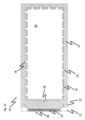
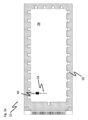
図2a-図2gは、本発明の一態様の上からの平面図を表し、等方性ガスケットが、AMEWODデバイスの上部プレートと下部プレートとの間にギャップを形成するために使用される。
図2aは、本発明の一態様による例示的なAMEWODデバイス(10)の上からの平面図を示し、液体試料は、上部基板のエッジに沿ってデバイスに導入される。AMEWODデバイス(10)は、下部基板(12)、ガスケット(14)、上部基板(16)、ポート(18、28)、エッジコネクタ(20)およびコンタクトパッド(22)を備える。明確にするために、図2bはガスケット(14)および上部基板(16)のみを示し、図2cは下部基板のみを示す。図2cの線23は、デバイスのアクティブ領域の境界を示す。
2a-2g show top plan views of one embodiment of the present invention in which an isotropic gasket is used to form a gap between the top and bottom plates of an AMEWOD device.
Figure 2a shows a top plan view of an exemplary AMEWOD device (10) according to one embodiment of the present invention, where a liquid sample is introduced into the device along the edge of the top substrate. The AMEWOD device (10) comprises a bottom substrate (12), a gasket (14), a top substrate (16), ports (18, 28), edge connectors (20) and contact pads (22). For clarity, Figure 2b shows only the gasket (14) and top substrate (16), and Figure 2c shows only the bottom substrate. The
EWODデバイスの流体チャンバは、ガスケットの内側の開口またはボアに対応する。流体チャンバの境界は、下部基板、上部基板、およびガスケットの内側エッジ面によって画定される。 The fluid chamber of the EWOD device corresponds to an opening or bore inside the gasket. The boundaries of the fluid chamber are defined by the inner edge surfaces of the lower substrate, the upper substrate, and the gasket.
エッジコネクタ(20)は、複数の接点(24)を備える。典型的には、AMEWODデバイス(10)は、液体試料(典型的には極性液体試料)を適用するための複数のポート(18)と、充填流体(図示せず)を適用するための単一のポート(28)とを備える。充填流体は、典型的には非極性流体であり、その非限定的な例としては、シリコーンオイル、フルオロシリコーンオイル、ペンタン、ヘキサン、オクタン、デカン、ドデカン、ペンタデカン、ヘキサデカンを含み、これらは一般にオイルと称され得る。図2の態様によれば、ポート(18、28)は、ガスケット(14)のエッジプロファイル構成及び上部基板(16)のエッジ(16a)によって画定される。したがって、ポート(18、28)は、下部基板(12)と上部基板(16)との間に画定されたキャビティ(26)内に液体試料をロードすることを可能にし、そのギャップの高さは、ガスケット(14)の厚さによって画定される。したがって、液体試料が導入される開口は、ガスケットの内側エッジ面14aと、上部基板(16)の外側エッジ16aによって画定される。
The edge connector (20) comprises a plurality of contacts (24). Typically, the AMEWOD device (10) comprises a plurality of ports (18) for applying a liquid sample (typically a polar liquid sample) and a single port (28) for applying a fill fluid (not shown). The fill fluid is typically a non-polar fluid, non-limiting examples of which include silicone oil, fluorosilicone oil, pentane, hexane, octane, decane, dodecane, pentadecane, and hexadecane, which may generally be referred to as oil. According to the embodiment of FIG. 2, the ports (18, 28) are defined by the edge profile configuration of the gasket (14) and the edge (16a) of the top substrate (16). The ports (18, 28) thus allow the liquid sample to be loaded into a cavity (26) defined between the bottom substrate (12) and the top substrate (16), the height of the gap being defined by the thickness of the gasket (14). Thus, the opening through which the liquid sample is introduced is defined by the
図2a-図2cの実施形態では、図2bに示すように、ガスケット14の内側エッジ面14aは、内側に(すなわち、流体チャンバの内部の方向に)向けられた突出部14bを含むエッジプロファイル構成を備え、AM-EWODデバイスが組み立てられたときに、突出部14bは上部基板16と重なり、一方、2つの隣接する突出部の間のガスケットの領域は上部基板16と重ならず、それによって、流体入力ポート18、28が形成される(あるいは、ガスケットは、内側エッジ14a内に画定された窪み14cを有するとして理解することができる。)。ガスケットの内側エッジ14aおよび上部基板のエッジ16aは、図2aまたは図2bに示される特定の配置に限定されない。ガスケットの内側エッジ14aおよび基板のエッジの少なくとも1つが直線ではなく、その結果、上部基板16と重ならないガスケットの少なくとも1つの領域が存在し、それによってポート18を形成しているのであれば、他の配置が使用されてもよい。図2bは、流体チャンバの略矩形の外周を画定するガスケットの内側エッジ面14aを有する流体チャンバを、略矩形として示しているが、本発明は、原理的には、矩形の流体チャンバに限定されない。
2a-2c, as shown in FIG. 2b, the
下部基板(12)、ガスケット(14)の内側エッジ面14a、および上部基板(16)は、それらの間にキャビティ(26)を画定し、このキャビティは、ガスケット(14)の厚さによって決定される高さh、ならびに内側エッジ長寸法によって画定される幅wおよび長さlを有する。ここで、高さhは、好ましくは、少なくとも約25μm、少なくとも約50μm、少なくとも約75μm、少なくとも約100μm、少なくとも約150μm、少なくとも約200μm、少なくとも約250μm、少なくとも約300μm、少なくとも約400μm、少なくとも約500μm、少なくとも約600μm、少なくとも約700μm、少なくとも約800μm、少なくとも約900μm、少なくとも約1000μmであり、幅wは、好ましくは、少なくとも約5mm、少なくとも約7.5mm、少なくとも約10mm、少なくとも約12.5mm、少なくとも約15mm、少なくとも約17.5mm、少なくとも約20mm、少なくとも約22.5mm、少なくとも約25mm、少なくとも約27.5mm、少なくとも約30mm、少なくとも約32.5mm、少なくとも約35mm、少なくとも約37.5mm、少なくとも約40mm、少なくとも約50mm、少なくとも約55mm、少なくとも約60mm、少なくとも約65mm、少なくとも約70mm、少なくとも約75mm、少なくとも約80mm、少なくとも約85mm、少なくとも約90mm、少なくとも約95mm、少なくとも約100mm、少なくとも約125mm、少なくとも約150mm、少なくとも約175mm、少なくとも約200mmである。長さlは、好ましくは、少なくとも約10mm、少なくとも約15mm、少なくとも約20μm、少なくとも約25mm、少なくとも約30mm、少なくとも約35mm、少なくとも約40mm、少なくとも約45mm、少なくとも約50mm、少なくとも約55mm、少なくとも約60mm、少なくとも約65mm、少なくとも約70mm、少なくとも約75mm、少なくとも約80mm、少なくとも約85mm、少なくとも約90mm、少なくとも約95mm、少なくとも約100mm、少なくとも約125mm、少なくとも約150mm、少なくとも約175mm、少なくとも約200mmである。使用にあたり、極性液体試料がデバイスに適用される前は、一般的には、キャビティ(26)はオイルで満たされる。
The lower substrate (12), the
この実施形態では、ガスケット14は、等方性で電気的に導電性のガスケット(14)である。ガスケットは、導電性材料から形成され、導電性材料の例としては、メタル、カーボン、またはメタルもしくはカーボン粒子を含む材料を含む。一般に、上部基板と下部基板とを電気的に接触させるために、ガスケット材料のバルク(bulk)をその表面に接続するための何らかの媒体が存在しなければならない。例えば、ガスケットは、SEM測定用の試料を実装するために使用されるような、テープの両面上に導電性接着剤を含む両面カーボンテープであってもよい。あるいは、ガスケットは、銀含有塗料または接着剤のような導電性接着剤またはペーストを介して上部および下部基板に電気的に接触する、非接着性の金属層から構成されてもよい。ガスケットは、電流がその厚さ全体にわたって自由に流れることができるように、一般的には、その構造組成に関して均一であり、特にその導電性成分の分布に関して均一である。等方性ガスケット(14)は、コンタクトパッド(22)と上部基板(16)上の少なくとも1つの導電性要素(図示せず)との間に導電性経路を形成する。
In this embodiment, the
下部基板(12)は、誘電体絶縁層によって被覆され、少なくとも1つの導電性要素が配置された第1の主表面と、疎水性層(図示せず)とを有する。少なくとも1つの導電性要素は、エッジコネクタ(20)の少なくとも1つの接点(24)に接続される(AM-EWODデバイスの場合、関連する要素電極をそれぞれ有する複数のアレイ要素は、典型的には下部基板上に設けられる。各アレイ要素は、エッジコネクタ20の1つまたは複数の接点に接続される。)。誘電体層及び疎水性層によって覆われていないコンタクトパッド(22)は、例えばPCB(プリント回路板)コネクタのようなエッジコネクタ(20)の接点(24)に、導電的に接続される。上部基板(16)は、少なくとも1つの導電性要素が配置される主表面を有し、疎水性材料の層(図示せず)によって覆われている。上部基板(16)上の少なくとも1つの導電性要素は、等方性ガスケット(14)と接触する位置では疎水性層を有していない。したがって、等方性ガスケット(14)は、コンタクトパッド(22)を介して、下部基板上のエッジコネクタ20の接点(24)と、上部基板(16)上の少なくとも1つの導電性要素との間で、導電性経路を形成する(図2aに示すように、ガスケット14は、エッジコネクタ24の他のコネクタ20のいずれにも重ならない。)。導電性要素を有する下部基板(12)及び上部基板(16)のそれぞれの表面は、対向配置で保持され、ギャップ距離は、等方性ガスケット(14)によって画定される。これは、図2aのデバイスの部分断面図である図2dに示されている(誘電体層、絶縁層、及び接点24、エッジコネクタ20は、説明を容易にするために図2dから省略されている)。
The lower substrate (12) has a first major surface covered by a dielectric insulating layer and on which at least one conductive element is disposed, and a hydrophobic layer (not shown). The at least one conductive element is connected to at least one contact (24) of the edge connector (20). (For AM-EWOD devices, a plurality of array elements, each with an associated element electrode, are typically provided on the lower substrate. Each array element is connected to one or more contacts of the
例えば生理食塩水のような極性液体などの液体の液滴がキャビティ(26)内に存在する場合、液滴が、下部基板(12)および上部基板(16)上のそれぞれの導電性素子間にブリッジを形成すると、容量結合回路が形成される。したがって、このような液滴は、例えば米国特許出願公開第2018/0284423号(その内容は参照により本明細書に組み込まれる)に記載されているように、エレクトロウェッティングにより制御することができる。
図2e-図2gは、図2aのAM-EWODデバイスを示しており、予めポート(28)を介してオイルで少なくとも部分的に充填された流体チャンバ内26に、AMEWODデバイス(10)のポート(18または類似のもの)を通して液体試料(30)を導入した後の図である。液体試料(30)は、例えば、ピペットまたはシリンジ(図示せず)を使用して、ポート(18)を通して導入することができる。最初に(図2e)、ポート(18)を通して液体試料(30)を適用した後、液体試料(30)は、エレクトロウェッティングによってキャビティ(26)内に移送され得る。マイクロプロセッサ(図示せず)は、スクリプトを用いて、エレクトロウェッティングによって極性液体の試料の移動を制御するように設計されたプロトコルを動作させるように構成され得る。
When a droplet of liquid, e.g., a polar liquid such as saline, is present in the cavity (26), a capacitive coupling circuit is formed when the droplet forms a bridge between the respective conductive elements on the lower substrate (12) and the upper substrate (16). Such droplets can therefore be controlled by electrowetting, as described, for example, in U.S. Patent Application Publication No. 2018/0284423, the contents of which are incorporated herein by reference.
2e-g show the AM-EWOD device of FIG. 2a after introducing a liquid sample (30) through port (18 or similar) of the AM-EWOD device (10) into the
液体試料(30)がキャビティ(26)に入ると、液体試料(30)はエレクトロウェッティングによって移動し、キャビティ(26)内で露出している等方性ガスケット(14)のエッジ要素(32)と接触することができる(図2f)。液体試料(30)が、等方性ガスケット(14)のエッジ要素(32)と接触するとき、液体試料(30)にチャージ電圧を印加することができる。チャージ電圧は、下部基板(12)の導電性要素(例えば、アレイ要素電極)と等方性ガスケット(14)のエッジ要素(32)との間に印加することができる。液体試料(30)が、エッジ要素(32)と接触した後にチャージされると、液体試料(30)は、エレクトロウェッティングによってキャビティ(26)内の別の位置に移動することができる。参照により本明細書に組み込まれる、2017年7月27日に出願された米国特許出願第15/661609号を有する本出願人の同時係属出願は、流体リザーバをプリチャージするためのプリチャージ構造を有する誘電体エレクトロウェッティング(EWOD)デバイスを記載している。 When the liquid sample (30) enters the cavity (26), it can move by electrowetting and come into contact with the edge elements (32) of the isotropic gasket (14) exposed in the cavity (26) (FIG. 2f). When the liquid sample (30) comes into contact with the edge elements (32) of the isotropic gasket (14), a charging voltage can be applied to the liquid sample (30). The charging voltage can be applied between the conductive elements (e.g., array element electrodes) of the lower substrate (12) and the edge elements (32) of the isotropic gasket (14). When the liquid sample (30) is charged after coming into contact with the edge elements (32), it can move to another location in the cavity (26) by electrowetting. Applicant's co-pending application, U.S. Patent Application No. 15/661,609, filed July 27, 2017, which is incorporated herein by reference, describes an electrowetting on dielectric (EWOD) device having a precharge structure for precharging a fluid reservoir.
図2gは、エッジ要素(32)と接触して液体試料(30)のチャージが行われた後、液体試料(30)から個々の液滴(34)を分注するところを示している。エッジ要素(32)との接触を通じた液体試料(30)のチャージは、液体試料(30)と、キャビティ(26)を充填するために使用されるオイルとの間の界面における表面張力特性を変更することができる。スクリプトによって構成されたマイクロプロセッサ(図示せず)により、エレクトロウェッティングの「分注」シーケンスがAMEWODデバイス(10)に適用されるとき、液滴(34)が液体試料(30)から分離されるときの効率は、エッジ要素(32)との接触時にチャージされていない液体試料と比較して、改善される。液体試料をチャージすることの有益な効果は、液体試料の組成に基づいて変化し得る。 2g shows dispensing of individual droplets (34) from the liquid sample (30) after charging of the liquid sample (30) in contact with the edge element (32). Charging the liquid sample (30) through contact with the edge element (32) can modify the surface tension characteristics at the interface between the liquid sample (30) and the oil used to fill the cavity (26). When an electrowetting "dispense" sequence is applied to the AMEWOD device (10) by a scripted microprocessor (not shown), the efficiency with which the droplets (34) are separated from the liquid sample (30) is improved compared to a liquid sample that is not charged upon contact with the edge element (32). The beneficial effect of charging the liquid sample can vary based on the composition of the liquid sample.
変形例(図示せず)では、図2bに示すガスケットは、デバイスの周囲に沿って電気的に連続ではなく、(例えば、非導電性接着剤を使用して)互いに絶縁された2つの導電性部分で構成されており、各部分は、下部基板上のトッププレートビア構造22のうちの1つに取り付けられている。この実施形態では、エッジコネクタから、1つのビアを通り、共通電極を通り、および、他方のビア22を通してエッジコネクタの別の端子に戻るような導通試験を遠隔で実行することも可能であり、結果として、トッププレートへの電気的接続を試験することができる。
In a variation (not shown), the gasket shown in FIG. 2b is not electrically continuous around the perimeter of the device, but is instead made up of two conductive sections insulated from each other (e.g., using a non-conductive adhesive), with each section attached to one of the top plate via
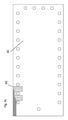
図3a-図3eは、本発明のさらなる態様を示しており、液体試料は、上部基板の表面の1つまたは複数の開口部を通してAMEWODデバイス(10)に適用される。そのような態様では、1つまたは複数の開口部18は、上部基板(16)内に提供され、等方性ガスケット(14)の内周に沿ったエッジプロファイル構成に合わせて整列する。図3aは、この実施形態によるデバイスの平面図であり、図3bは、説明を容易にするために上部基板を別個に示す。この実施形態のガスケット14および下部基板は、それぞれ図2bおよび図2cのガスケット14および下部基板に概ね対応する。
Figures 3a-e show a further aspect of the invention, where a liquid sample is applied to an AMEWOD device (10) through one or more openings in the surface of the top substrate. In such an aspect, one or
したがって、液体試料は、(図2に示される態様のポート(18、28)と比較すると)上部基板(16)の開口部を通って、AMEWODデバイス(10)に入ることができる。図2a-図2cでは、上部基板(16)は、等方性ガスケット(14)の長さと幅よりも小さい長さと幅を有し、上部基板(16)のエッジは、キャビティ(26)を画定するガスケットの内側エッジの付近で、等方性ガスケット(14)のエッジプロファイル構成を二分するように構成されている。図3に示される発明の態様によれば、上部基板(16)は、等方性ガスケット(14)の長さと幅に等しい、あるいは、実質的に等しい長さと幅を有する。 Thus, the liquid sample can enter the AMEWOD device (10) through an opening in the top substrate (16) (compare ports (18, 28) in the embodiment shown in FIG. 2). In FIGS. 2a-c, the top substrate (16) has a length and width that are less than the length and width of the isotropic gasket (14), and the edge of the top substrate (16) is configured to bisect the edge profile configuration of the isotropic gasket (14) near the inner edge of the gasket that defines the cavity (26). According to the embodiment of the invention shown in FIG. 3, the top substrate (16) has a length and width that are equal or substantially equal to the length and width of the isotropic gasket (14).
図3aは、液体試料を導入する前の、本発明のさらなる態様によるAMEWODデバイス(10)の上からの平面図を示す。ポート(18、28)は、上部基板(16)の周囲に沿って配置され、それらは、等方性ガスケット(14)の隣接するエッジプロファイル構成の間にある領域と一致する。ポート(18、28)は、典型的には、基板に穴をあけることによって提供される。上部基板(16)に適用された疎水性コーティング(図示せず)は、組み立てられたデバイスにおいて、ガスケット(14)に相当する少なくとも1つの領域において除去され、それによって、(エッジコネクタのそれぞれの端子と接続されている)下部基板上の接点(22)から、等方性ガスケット(14)と接触している上部基板(16)の表面上の少なくとも1つの導電性要素までの導電性経路を形成する。 Figure 3a shows a top plan view of an AMEWOD device (10) according to a further embodiment of the invention prior to the introduction of a liquid sample. The ports (18, 28) are arranged along the periphery of the upper substrate (16) and coincide with the areas between adjacent edge profile configurations of the isotropic gasket (14). The ports (18, 28) are typically provided by drilling holes in the substrate. A hydrophobic coating (not shown) applied to the upper substrate (16) is removed in at least one area corresponding to the gasket (14) in the assembled device, thereby forming a conductive path from the contacts (22) on the lower substrate (connected with the respective terminals of the edge connector) to at least one conductive element on the surface of the upper substrate (16) in contact with the isotropic gasket (14).
図3c-図3eは、上部基板(16)の表面の開口(18または類似のもの)を通ってAMEWODデバイス(10)に導入される液滴(30)の経過を示す。液滴(30)は、ポート(18)を通して適用されると、最初にEWODによってキャビティ(26)内に移動され(図3c)、その後、液滴(30)は、等方性ガスケット(14)のエッジ要素(32)に接触するように移動される(図3d)。エッジ要素(32)と接触している間に、液滴をチャージするために、電圧が液滴(30)に印加される。エッジ要素(32)との接触に続いて、液滴(30)がチャージされると、液滴(30)は、EWODによってキャビティ(26)内のさらなる位置に再び移動する(図3e)。スクリプト(図示せず)を動作させるように構成されたマイクロプロセッサは、液滴(34)を液体試料(30)から分注させる。次いで、液滴(34)は、その意図された用途に従って、AMEWODデバイス(10)内のさらなる反応プロセスまたはスキームのために使用され得る。 Figures 3c-e show the progression of a droplet (30) being introduced into the AMEWOD device (10) through an opening (18 or similar) in the surface of the upper substrate (16). When the droplet (30) is applied through the port (18), it is first moved by the EWOD into the cavity (26) (Figure 3c), after which the droplet (30) is moved to contact an edge element (32) of the isotropic gasket (14) (Figure 3d). While in contact with the edge element (32), a voltage is applied to the droplet (30) to charge it. Following contact with the edge element (32), once the droplet (30) is charged, the droplet (30) is again moved by the EWOD to a further location in the cavity (26) (Figure 3e). A microprocessor configured to run a script (not shown) causes the droplet (34) to be dispensed from the liquid sample (30). The droplets (34) can then be used for further reaction processes or schemes within the AMEWOD device (10) according to their intended use.
図2および図3の実施形態では、ガスケット14は、バルク導電性材料から作製されているという点で「等方性」であり、したがって、ガスケット内のある点における導電率は、あらゆる方向において同じ値または実質的に同じ値を有する(典型的には、ガスケット全体にわたって均一または概ね均一であってもよい)。(材料の「バルク」特性は、「示強性(intensive property)」とも呼ばれ、材料の局所的な物理的特性であり、その値は、測定される材料の量に依存しない。)。他の実施形態では、ガスケットは等方性ではなく、ガスケットの導電率は、ある意味で異方性であり、例えば、導電率は、絶縁領域によって分離された独立した導電性経路を画定するために、ガスケットの体積にわたって変化してもよく、または、ガスケットは、一方向のみ、または、一方向に少なくとも優先的に導電する材料から作製されてもよい。
2 and 3, the
図11aは、z方向(図11aにおける垂直方向)に電導するが、x方向およびy方向に沿って電導しない材料で作製されたガスケットを有するマイクロ流体デバイスの断面図であり、これは「z電導スペーサ(z-conducting spacer)」として知られている。上部基板上には複数の電極があり、これらは、(図11aでは「EWOD基板」として記載されている)下部基板上の対応する電極セットによってアドレス指定され、下部基板上のコネクタ(例えば、図2および図3のものと同様のエッジコネクタなど)のそれぞれの端子に接続される。ガスケットは、z方向に垂直な方向に最小の導電率を有し、z方向では複数の電極を短絡させる。したがって、ガスケットは、上部基板上の電極を下部基板上の対応する電極に電気的に接続するビア領域を提供し、一方、上部基板上の電極が下部基板上の他の電極から絶縁されることを確実にする。そのような異方性ガスケットは、異方性導電性フィルム(ACF)またはペースト(ACP)自体を使用するか(したがってガスケットは異方性導電性材料のバルクで形成される)、または、一方向のみの導電を可能にするようなガスケットの構造的特徴に併せて異方性導電性フィルム(ACF)またはペースト(ACP)を使用することによって、達成することができる。異方性ガスケットを作製する別の方法は、FPC(フラットプリント回路)を作製するために使用される従来の方法によることができ、この場合、ビアは銅から作製され、その間の絶縁部分はKapton(商標)から作製される。 11a is a cross-sectional view of a microfluidic device with a gasket made of a material that is conductive in the z-direction (vertical in FIG. 11a) but not along the x- and y-directions, known as a "z-conducting spacer." There are electrodes on the top substrate that are addressed by a corresponding set of electrodes on the bottom substrate (labeled as "EWOD substrate" in FIG. 11a) and connected to respective terminals of a connector (such as an edge connector similar to those in FIGS. 2 and 3) on the bottom substrate. The gasket has minimal conductivity perpendicular to the z-direction and shorts the electrodes in the z-direction. Thus, the gasket provides via areas that electrically connect the electrodes on the top substrate to the corresponding electrodes on the bottom substrate while ensuring that the electrodes on the top substrate are insulated from other electrodes on the bottom substrate. Such an anisotropic gasket can be achieved by using an anisotropic conductive film (ACF) or paste (ACP) by itself (so that the gasket is formed of a bulk of anisotropic conductive material) or by using an anisotropic conductive film (ACF) or paste (ACP) in conjunction with structural features of the gasket that allow electrical conduction in only one direction. Another method of making an anisotropic gasket can be by the traditional method used to make FPCs (flat printed circuits), where the vias are made from copper and the insulating parts between them are made from Kapton™.
図11bは、2つの対向する基板上の電極の「x-y」位置が一致していない実施形態を示し、したがって、ガスケットは、z方向(ガスケットの厚さ方向)に延在するとともに、一方の基板上の電極と他方の基板上の電極との間に電気的接続を提供するためにガスケットの平面(x-y平面)内に延在する、導電性経路の「x-y」接続ルーティングを提供するために、より複雑な設計を必要とする。これは、例えば、下部基板上の電極から、上部基板上の対応する電極の下方にある下部基板上の点への電気的接続を提供する、FPCなどのパターン化された導電層を提供することによって達成することができる。上部基板上の電極への電気的接続は、ガスケットに設けられたビアによって、例えば、z方向に電導するが、x方向およびy方向には電導しない材料で形成されたガスケットを使用することによって、または、本明細書に記載された他の技法によって、完成される。 11b shows an embodiment in which the "x-y" locations of the electrodes on the two opposing substrates are not coincident, and therefore the gasket requires a more complex design to provide "x-y" connection routing of conductive paths that extend in the z direction (through the thickness of the gasket) and in the plane of the gasket (the x-y plane) to provide electrical connection between the electrodes on one substrate and the electrodes on the other substrate. This can be accomplished, for example, by providing a patterned conductive layer, such as an FPC, that provides electrical connection from the electrodes on the lower substrate to points on the lower substrate that are below the corresponding electrodes on the upper substrate. Electrical connection to the electrodes on the upper substrate is completed by vias in the gasket, for example, by using a gasket made of a material that is conductive in the z direction but not in the x and y directions, or by other techniques described herein.
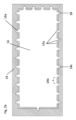
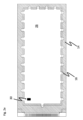
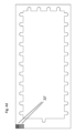
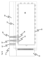
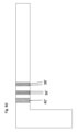
本発明のさらに別の態様では、図4a-図4fにおいて、AMEWODデバイス(10)が、上から見た平面図で示されている。図4aは、図3に示されている態様と同様のAMEWODデバイス(10)を概略的に示しているが、いくつかの修正が加えられている。図4bは、図4aに示す破線に沿った図4aのデバイスの断面図である。図4aに示されるように、上部基板(16)は、等方性ガスケット(14)の外側寸法まで延在する。 In yet another embodiment of the present invention, an AMEWOD device (10) is shown in top plan view in Figs. 4a-4f. Fig. 4a shows a schematic of an AMEWOD device (10) similar to the embodiment shown in Fig. 3, but with some modifications. Fig. 4b shows a cross-sectional view of the device of Fig. 4a taken along the dashed line shown in Fig. 4a. As shown in Fig. 4a, the top substrate (16) extends to the outer dimension of the isotropic gasket (14).
図4cには、上部基板(16)が、別個に図示されている。図4aおよび図4cに示されるように、上部基板は電極対(36, 38)の配列を備えており、電極対(36, 38)は、上部基板のエッジ付近に設けられていてもよい。図4bに示されるように、導電層41は、上部基板16の表面上に置かれてもよく、この導電層は、電極対を画定するようにパターニングされてもよい。導電層の残りの部分は、共通電極などの連続的な導電性要素を提供するために使用されてもよい。図4aおよび図4cに示すように、電極対の電極は、ガスケットを越えて流体チャンバに飛び出ている。図4aおよび図4cは、流体チャンバの境界に対してほぼ垂直に延在する電極対の電極を示しているが、実施形態はこれに限定されない。電極対の電極は、上部基板のエッジに延在するおのおのの導電性トラックを備える(あるいは、おのおのの導電性トラックに接続される)。図4aの図では、簡略化のために、2つの電極対(36、38)が示されているが、より少ない、またはより多い電極対(36、38)が提供されてもよいことが理解されるであろう。例えば、一対の電極は、ガスケット(14)の各エッジプロファイル要素(32)と対応するように提供されてもよい。複数の電極対(36、38)は、単一のエッジプロファイル要素(32)上に設けられてもよく、または順列(in permutations)で設けられてもよく、例えば、1つのエッジプロファイル要素が単一の電極対を含んでもよく、1つのエッジプロファイル要素が2つ以上の電極対を含んでもよく、さらに別のエッジプロファイル要素が電極対を有さなくてもよいことが、さらに理解されよう。さらに別の態様では、複数の個別の正端子の対として作用する、負端子などの共通端子が実装されてもよい。
In FIG. 4c, the top substrate (16) is shown separately. As shown in FIGS. 4a and 4c, the top substrate comprises an array of electrode pairs (36, 38), which may be located near the edge of the top substrate. As shown in FIG. 4b, a
図4dに示すように、ガスケットには導電性部分22'が設けられており、この導電性部分22'は、デバイスが組み立てられたときに、上部基板上の導電性トラックのそれぞれと接触するとともに、下部基板上の対応する導電性トラックとも接触する(図4eに別個に示されている)。したがって、電極対(36、38)の電極は、制御機器(図示せず)への接続のために、それぞれの導電性ブリッジ(22')を介して、下部基板(12)のエッジ上の延長エッジコネクタ(20')の接点に電気的に結合することができる。キャビティ(26)に近接する上部基板(16)は、本明細書で上述したような連続的な導電性要素を備えてもよいが、電極対の電極が、互いに絶縁され、かつ、連続的な導電性要素から電気的に絶縁されるように、電極対(36、38)の周囲の領域は、絶縁領域(40)を備え得る。
それぞれの各電極対(36、38)は、i)液滴の電流測定または電位差測定などの電気化学測定を行うこと、ii)液滴にチャージ電圧を印加すること、iii)液滴のインピーダンス特性を決定すること、を含む、様々な目的のために使用されることができるが、これらに限定されない。図4fは、電極対(36、38)のそれぞれの各電極における液滴(42)の存在を示す。各液滴(42)の特性は、適切な測定プロセスによって適宜に決定されてもよいし、または、チャージ電圧がそのような液滴に印加されてもよい。
As shown in Fig. 4d, the gasket is provided with conductive portions 22' which, when the device is assembled, contact each of the conductive tracks on the upper substrate and also contact corresponding conductive tracks on the lower substrate (shown separately in Fig. 4e). Thus, the electrodes of the electrode pairs (36, 38) can be electrically coupled through their respective conductive bridges (22') to contacts of the extended edge connector (20') on the edge of the lower substrate (12) for connection to a control device (not shown). The upper substrate (16) adjacent the cavity (26) may comprise a continuous conductive element as described herein above, but the area around the electrode pairs (36, 38) may comprise an insulating region (40) such that the electrodes of the electrode pairs are electrically insulated from each other and from the continuous conductive element.
Each respective electrode pair (36, 38) can be used for a variety of purposes, including, but not limited to, i) performing electrochemical measurements, such as amperometric or potentiometric measurements, of the droplets, ii) applying a charging voltage to the droplets, and iii) determining impedance characteristics of the droplets. Figure 4f illustrates the presence of a droplet (42) at each respective electrode of each electrode pair (36, 38). The characteristics of each droplet (42) may be suitably determined by a suitable measurement process or a charging voltage may be applied to such droplet.
Schlicht他は、「マイクロ流体受動ネットワークにおける液滴-界面-二重層の分析評価(Droplet-interface-bilayer assays in microfluidic passive networks)」(Scientific Reports, (2015) v5 pp9951)を記載している。本発明のさらなる態様では、液滴(42)のそれぞれの対が、接触し、その後に安定な液滴界面二重層(DIBs)を形成できるように、EWODによって操作されてもよい。次いで、そのような液滴の対は、EWODによって移動し、それぞれの各電極対(36、38)に接触することができる。それぞれの液滴がそれぞれの電極と接触し、DIBを形成した一対の液滴(42)が電極対(42)と接触した状態で保持されると、DIB界面を横切って回路が形成される。そして、電極対(36、38)は、DIB界面を横切って1つの液滴から別の液滴への溶質の移送をモニタするために使用され、固定電圧が電極対(36、38)の間に印加されたときに流れる電流の変化として検出される。 Schlicht et al. describe "Droplet-interface-bilayer assays in microfluidic passive networks" (Scientific Reports, (2015) v5 pp9951). In a further aspect of the invention, each pair of droplets (42) may be manipulated by EWOD to contact and subsequently form stable droplet interface bilayers (DIBs). Such droplet pairs may then be moved by EWOD to contact each respective electrode pair (36, 38). When each droplet is in contact with a respective electrode and the pair of droplets (42) that have formed a DIB are held in contact with the electrode pair (42), a circuit is formed across the DIB interface. The electrode pair (36, 38) is then used to monitor the transport of solutes from one droplet to another across the DIB interface, detected as a change in current flow when a fixed voltage is applied between the electrode pair (36, 38).
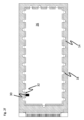
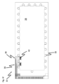
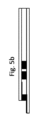
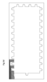
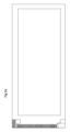
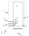
代替実施形態では、上部基板上の(液滴と接触する)測定パッドと下部基板上の対応するパッドとの間において必要な導電性の電極経路は、(図4のように)上部基板と下部基板との間で垂直に位置合わせされたパッドへの上部基板内のトラックとは対照的に、ガスケット内に設けられた導電性トラックを介して作製される。この実施形態は、図5a-図5eに図示されている。図5aは、この実施形態によるEWODデバイスの上からの平面図であり、図2に関して説明したように、上部基板(16)のエッジが、キャビティ(26)を画定するガスケットの内側エッジに沿って等方性ガスケット(14)のエッジプロファイル構成を二分するように、上部基板(16)が、等方性ガスケット(14)よりも小さい長さと幅の寸法を備える場合を示す。したがって、ポート(18)は、上部基板(16)のエッジおよび等方性ガスケット(14)のエッジ構造によって画定される。 In an alternative embodiment, the necessary conductive electrode paths between the measurement pads (in contact with the droplet) on the top substrate and the corresponding pads on the bottom substrate are created via conductive tracks in the gasket, as opposed to tracks in the top substrate to pads aligned vertically between the top and bottom substrates (as in FIG. 4). This embodiment is illustrated in FIGS. 5a-5e. FIG. 5a is a top plan view of an EWOD device according to this embodiment, where the top substrate (16) has smaller length and width dimensions than the isotropic gasket (14), as described with respect to FIG. 2, such that the edge of the top substrate (16) bisects the edge profile configuration of the isotropic gasket (14) along the inner edge of the gasket that defines the cavity (26). Thus, the port (18) is defined by the edge of the top substrate (16) and the edge structure of the isotropic gasket (14).
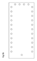
図5aに示される電極対(36、38)は、図4に示される態様とは異なるように構成される。上部基板の平面図である図5cに示されるように、上部基板(16)上に露出し、キャビティ(26)に延びる各電極対(36、38)の部分は、上部基板の平面図である図5cに示されるように、それらが下部基板(12)に面する上部基板(16)の表面上に配置された導電層内に画定される限りにおいて、図4のものと同様に作製される。しかしながら、ガスケットの平面図である図5dに示されるように、電極対トラック(36'、38')は、ガスケット(14)内/上に設けられる。デバイスがアセンブルされるとき、ガスケット内/上に設けられた電極トラックは、上部基板(16)上の電極対(36、38)と電気的に接触し、導電性ブリッジ(22')を介して、下部基板(12)上の延長エッジコネクタ(20')の端子に電気的に接触する(必要であれば、それぞれの部分は互いに直接結合されてもよいが、それらの間に導電性経路が存在する限り、互いに物理的に結合される必要はない。)。下部基板は、図5eに平面図で示されている(図5eの内側の長方形は流体チャンバの境界を示す)。図5bは、図5aに示された破線に沿ったEWODデバイスの部分断面図であり、図5bには、ガスケット内/上に設けられた電極トラックと、上部基板(16)上の電極対(36、38)と、下部基板上の延長エッジコネクタ(20')の端子との間の電気的接続も示されている。 The electrode pairs (36, 38) shown in Fig. 5a are constructed differently than the embodiment shown in Fig. 4. As shown in Fig. 5c, a top view of the top substrate, the portions of each electrode pair (36, 38) exposed on the top substrate (16) and extending into the cavity (26) are fabricated similarly to those in Fig. 4 in so far as they are defined in a conductive layer disposed on the surface of the top substrate (16) facing the bottom substrate (12), as shown in Fig. 5c, a top view of the top substrate. However, as shown in Fig. 5d, a top view of the gasket, the electrode pair tracks (36', 38') are provided in/on the gasket (14). When the device is assembled, the electrode tracks in/on the gasket make electrical contact with the electrode pairs (36, 38) on the top substrate (16) and, via the conductive bridges (22'), with the terminals of the extended edge connector (20') on the bottom substrate (12). (The parts can be directly connected to each other if necessary, but they do not need to be physically connected to each other as long as there is a conductive path between them.) The bottom substrate is shown in plan view in FIG. 5e (the inner rectangle in FIG. 5e indicates the boundary of the fluid chamber). FIG. 5b is a partial cross-sectional view of the EWOD device along the dashed line shown in FIG. 5a, and also shows the electrical connections between the electrode tracks in/on the gasket, the electrode pairs (36, 38) on the top substrate (16), and the terminals of the extended edge connector (20') on the bottom substrate.
これまで説明してきた構造では、目標は、上部基板上の1つまたは複数の電極を下部基板上の対応する端子に接続することであり、これは、異なるタイプのガスケットを介して達成された。これを行う1つの理由は、単一の電気的接続が、デバイスを駆動する機器内の電子基板と下部基板との間に作製され、上部基板上のコンポーネントへの電気的接続は、下部基板上の端子からガスケットを介して行われ、機器への接続のための端子を上部基板上に設ける必要がないためである。この電気的接続は、フレキシブルプリント回路(FPC)コネクタ又はプリント回路板(PCB)コネクタを含む様々な方法で行うことができる。エッジコネクタ(20)内の接点(24)の数が非常に多く、それぞれの各接点(24)の幅及びそれらの間のスペースが狭くなりすぎる場合には、それぞれの各接点(24)と機器内の受信コネクタ(図示せず)との間の良好な電気的接触が損なわれることがある。そのような場合、1つまたは複数の追加のエッジコネクタ(図示せず)が、下部基板(12)の別のエッジ上(例えば、長いエッジ上)に提供され得る。 In the structures described so far, the goal is to connect one or more electrodes on the upper substrate to corresponding terminals on the lower substrate, which is accomplished through different types of gaskets. One reason for doing this is that a single electrical connection is made between the electronics board in the equipment driving the device and the lower substrate, and the electrical connection to the components on the upper substrate is made from the terminals on the lower substrate through the gasket, without the need for terminals on the upper substrate for connection to the equipment. This electrical connection can be made in a variety of ways, including flexible printed circuit (FPC) connectors or printed circuit board (PCB) connectors. If the number of contacts (24) in the edge connector (20) is so large that the width of each of the contacts (24) and the space between them becomes too narrow, good electrical contact between each of the contacts (24) and the receiving connector (not shown) in the equipment may be compromised. In such cases, one or more additional edge connectors (not shown) may be provided on another edge (e.g., on a long edge) of the lower substrate (12).
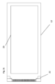
また、上部基板上のコンポーネントへの電気的接続は、異方性ガスケット(14’)内の導電性経路を通して、直接になされてもよい。上部基板(16)から導電性パッド(22'、40)を介して下部基板(12)上に、そして、下部基板上のエッジコネクタ(20)までの回路を通すのではなく、代わりに、エッジコネクタ(図示せず)をガスケット(14')の外側エッジに沿って設けてもよい。ガスケット(14')から上部基板(16)への電気的接続を直接形成することの潜在的な利点は、下部基板(12)の外形寸法を最小限に抑えることができることである。さらに、基板層間の導電性経路破損のおそれが低減される。その場合、例えば、この実施形態によるEWODデバイスの平面図である図6a、および、図6aのEWODデバイスのガスケットの平面図である図6bに示されるように、かなり単純なガスケットを使用することができる。EWODデバイスの上部基板は図5cの上部基板に対応し、共通電極および1つまたは複数の電極対36、38が設けられる。ガスケットには導電性経路25が設けられており、デバイスが組み立てられると、共通電極および1つまたは複数の電極対36、38は、ガスケット内/上のそれぞれの導電性経路と電気的に接触する。ここで示されるガスケットは、主要部分について非導電性であってもよいが、例えば、1つの表面のみにプリント回路を有し、「z」方向に局所的な電気伝導度(conductance)を生成する「ビア」構造がなくてもよい。
Alternatively, electrical connections to components on the upper substrate may be made directly through conductive paths in the anisotropic gasket (14'). Rather than passing a circuit from the upper substrate (16) through the conductive pads (22', 40) onto the lower substrate (12) and to an edge connector (20) on the lower substrate, an edge connector (not shown) may instead be provided along the outer edge of the gasket (14'). A potential advantage of forming electrical connections directly from the gasket (14') to the upper substrate (16) is that the overall dimensions of the lower substrate (12) may be minimized. Furthermore, the risk of conductive path breakage between substrate layers is reduced. In that case, a fairly simple gasket may be used, as shown, for example, in FIG. 6a, which is a plan view of an EWOD device according to this embodiment, and in FIG. 6b, which is a plan view of the gasket of the EWOD device of FIG. 6a. The upper substrate of the EWOD device corresponds to the upper substrate of FIG. 5c, and is provided with a common electrode and one or more electrode pairs 36, 38. The gasket is provided with
図6aのデバイスは、デバイスと機器との間の電気的インターフェースを提供するために、2つの独立したエッジコネクタ、または2つの部分を有するエッジコネクタを必要とし、一方のコネクタ(または部分)は、上部基板上に提供されるコンポーネントへの接続を行い、他方のコネクタ(または部分)は、下部基板上に提供される任意のコンポーネントへの電気的接続を行う。これは図6aの線20aによって示されており、エッジコネクタ20に2つの部分があることを示している。一方の部分は、下部基板上のみのコンポーネントへの接続を行い、他方の部分は、導電性トラック36'および38'への接続を含む上部基板のみへの接続を行う(この実施形態では、下部基板は、一般に従来のもの、例えば、TFT下部基板であってもよい)。
The device of FIG. 6a requires two separate edge connectors, or an edge connector with two parts, to provide an electrical interface between the device and the equipment, one connector (or part) for connection to components provided on the top substrate, and the other connector (or part) for electrical connection to any components provided on the bottom substrate. This is illustrated by
代替的な配置は、図7aおよび図7bに示されるように、下部基板および上部基板の両方への電気的接続を提供する単一のFPCコネクタを有しており、図7aは、この実施形態によるEWODデバイスの平面図であり、図7bは、ガスケット14'の平面図である。(上部基板からのトラックのみが示されており、下部基板上の導電性トラックは、エッジコネクタ20を除いて示されていない。)。ここで、異方性ガスケット14'は、下部基板(12)の境界を越えて延在する。このような異方性ガスケット(14')は、両側にプリント回路を有する絶縁層からなってもよい(それぞれ、一方の側のプリント回路は、下部基板への/からの信号を提供し、他方の側のプリント回路は、上部基板への/からの信号を提供する)。異方性ガスケット(14')の厚さは、エレクトロウェッティングデバイスのキャビティ(26)の高さを決定する。あるいは、外部電気接続は、エッジコネクタ20に引き戻されるのではなく、導電性トラック36'、38'を介してトッププレート電極36、38に直接行われてもよい。
An alternative arrangement has a single FPC connector providing electrical connections to both the bottom and top substrates, as shown in Fig. 7a and 7b, where Fig. 7a is a plan view of an EWOD device according to this embodiment, and Fig. 7b is a plan view of a gasket 14'. (Only the tracks from the top substrate are shown, the conductive tracks on the bottom substrate are not shown, except for the edge connector 20). Here, the anisotropic gasket 14' extends beyond the boundary of the bottom substrate (12). Such an anisotropic gasket (14') may consist of an insulating layer with printed circuits on both sides (one side of the printed circuits providing signals to/from the bottom substrate, and the other side of the printed circuits providing signals to/from the top substrate, respectively). The thickness of the anisotropic gasket (14') determines the height of the cavity (26) of the electrowetting device. Alternatively, the external electrical connections may be made directly to the
図8aは、本発明のさらなる実施形態によるEWODデバイスを示しており、ここでは、上部基板(16')(図8bに示される)は、下部基板(12)の長いエッジを覆う、延長された長いエッジプロファイルを含む。電極対(36、38)は、エッチングされて、キャビティ(26)に面する上部基板(16)の主表面上に設けられた導電層(ITO層など)となっている。図8aの場合には、上部基板(16')を下部基板(12)から分離するために使用されるガスケットは、それぞれの基板間に電気的ブリッジを形成しない。むしろ、FPCまたはPCBコネクタは、機器への接続のためにそれぞれの基板上の導電性トラックに直接結合され得る。図8cは、この例ではFPC(60)のコネクタ(図8dに示される)を備えた後のEWODデバイスを示し、コネクタは、上部基板(16')のそれぞれの要素に電気的に結合される導電性経路(36'、38'、40')を画定する。すなわち、コネクタ上の導電性経路36'、38'は、上部基板上のITO層に画定された電極対36、38の電極に接合され、残りの導電性経路(40')は、下部基板(12)上のTFT層の回路への対向電極または接地電極として作用する上部基板(16')上のITO層の主要部分への電気経路を形成する。図7aの実施形態では、外部の電気的接続は、エッジコネクタ20に戻る接続ではなく、導電性トラックを介してトッププレート電極36、38に直接行われてもよい。
Figure 8a shows an EWOD device according to a further embodiment of the invention, in which the top substrate (16') (shown in Figure 8b) includes an extended long edge profile that covers the long edge of the bottom substrate (12). Electrode pairs (36, 38) are etched into a conductive layer (such as an ITO layer) on the major surface of the top substrate (16) facing the cavity (26). In the case of Figure 8a, the gasket used to separate the top substrate (16') from the bottom substrate (12) does not form an electrical bridge between the respective substrates. Rather, FPC or PCB connectors can be directly bonded to conductive tracks on the respective substrates for connection to the equipment. Figure 8c shows the EWOD device after the connector (shown in Figure 8d), in this example an FPC (60), is provided, which defines conductive paths (36', 38', 40') that are electrically coupled to the respective elements of the top substrate (16'). That is, the conductive paths 36', 38' on the connector are bonded to the electrodes of the
本発明のさらなる態様では、図9a-図9bにおいて図示されるように、ディスクリートな導電性回路は、異方性ガスケット(14')内に備えられるが、キャビティ(26)に面する上部基板(16)の内面上には備えられない。そのような態様では、単一の導電層が、例えば、共通電極を形成するために、キャビティ(26)に面する上部基板(16)の表面全体にわたって備えられる。ガスケット14'は、導電性経路/パッド40を備えており、導電性経路/パッド40は、デバイスが組み立てられると、下部基板上のパッド22に接触し、上部基板の内面上の導電層にも接触する。異方性ガスケット(14')はまた、1つまたは複数の電極対(36"、38")を備え、その端は、液滴(42)の対によって接触され得る。この実施形態によるEWODのガスケットは、平面図で見たときに、図5dのガスケットに概ね対応し得るが、導電性経路36'、38'は、デバイスが組み立てられるとき、上部基板の内面上の導電層には接触せず、代わりに、流体チャンバ内の流体液滴42に接触し得る(例えば、導電性経路36'、38'は、以下の図10cに示されるように形成され得る)。
In a further embodiment of the invention, as illustrated in Figs. 9a-b, a discrete conductive circuit is provided within the anisotropic gasket (14'), but not on the inner surface of the upper substrate (16) facing the cavity (26). In such an embodiment, a single conductive layer is provided across the entire surface of the upper substrate (16) facing the cavity (26), for example to form a common electrode. The gasket 14' includes conductive paths/
いくつかの態様では、異方性ガスケット(14')は、複数の導電層が絶縁層を間に挟んで互いに上下に配置されるような積層構造中に、1以上の電極対(36''、38'')を備えてもよい。例えば、ガスケットは、多層状(multi-lamellar)であってもよく、これは、フレキシブルプリント回路に使用される一般的な構造である(一例として、https://kenvins.wordpress.com/2014/07/25/next-up-flexible-stackup-type-pcb/参照)。したがって、電極対のそれぞれは、キャビティ(26)のx平面またはz平面内で作動し得る。図9aに示すように、導電性経路は、図4及び図5について説明した方法で、ガスケットを通って下部基板までを接続される。しかしながら、導電性経路は、例えば図6について説明した方法で、外部コネクタに直接接続できることが理解されよう。 In some embodiments, the anisotropic gasket (14') may include one or more electrode pairs (36'', 38'') in a stacked structure, such that multiple conductive layers are disposed one above the other with an insulating layer in between. For example, the gasket may be multi-lamellar, a common structure used for flexible printed circuits (see, for example, https://kenvins.wordpress.com/2014/07/25/next-up-flexible-stackup-type-pcb/). Thus, each of the electrode pairs may operate in the x-plane or the z-plane of the cavity (26). As shown in FIG. 9a, the conductive paths are connected through the gasket to the underlying substrate in the manner described with respect to FIGS. 4 and 5. However, it will be appreciated that the conductive paths may be directly connected to an external connector, for example, in the manner described with respect to FIG. 6.
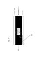
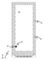
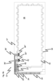
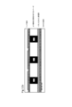
図10a-図10dに示されるように、異方性ガスケット(14')を利用する場合、導電性エッジ(50)が、下部基板(12)と上部基板(16)との間のギャップを画定するガスケットの内側エッジの周囲に提供されてもよい。導電性エッジ(50)は、図2eおよび図2fにて説明されるものと同様の方法で、それと接触する液体試料の電圧設定を達成するために使用されてもよい。延長エッジコネクタ(20')は、機器(図示せず)への接続のためにAMEWODデバイス(10)の端に電極対トラック(36'、38')を設けるために、エッジコネクタ(20)のいずれかの側に備えることができる。導電性エッジ(50)が、電極(36、38)に接触して、それらの間に短絡を形成しないことを確実にするために、導電性エッジが上部基板に接触しないことが必要であることに留意すべきである。同様の理由で、それが下部基板に接触することも不利であり得る。したがって、適切な構造は、外側層(the outer layers)が非導電性である少なくとも3つの層を含む層状ガスケットであってもよく、図10aの破線に沿った図10aのEWODの断面図である図10bに示されている。(この実施形態によるEWODのガスケットは、平面図で見たときの図5dのガスケットに概ね対応し得るが、電極対36、38が存在しているエッジプロファイル構成が、ガスケットの内側に向かってさらに突出している点で相違している)。 As shown in Figs. 10a-10d, when utilizing an anisotropic gasket (14'), a conductive edge (50) may be provided around the inner edge of the gasket that defines the gap between the lower substrate (12) and the upper substrate (16). The conductive edge (50) may be used to achieve voltage setting of a liquid sample in contact therewith in a manner similar to that described in Figs. 2e and 2f. An extended edge connector (20') may be provided on either side of the edge connector (20) to provide electrode pair tracks (36', 38') at the end of the AMEWOD device (10) for connection to an instrument (not shown). It should be noted that it is necessary for the conductive edge (50) not to contact the upper substrate to ensure that it does not contact the electrodes (36, 38) and form a short circuit between them. For similar reasons, it may also be disadvantageous for it to contact the lower substrate. A suitable structure may therefore be a layered gasket comprising at least three layers, the outer layers of which are non-conductive, as shown in Fig. 10b, which is a cross-sectional view of the EWOD of Fig. 10a taken along the dashed line of Fig. 10a. (The gasket of the EWOD according to this embodiment may generally correspond to the gasket of Fig. 5d when viewed in plan, with the difference being that the edge profile configuration where the electrode pairs 36, 38 are present protrudes further towards the inside of the gasket.)
本発明のさらなる態様では、先の実施形態のガスケット内の導電層は、図10cの別の第2断面に示されるように、下部基板上の活性領域を取り囲む領域の全てまたは大部分を覆うように、図10a-図10bに示される範囲を超えて延在することができる。この構造は、AMEWODデバイス(10)のユーザまたは環境のいずれかからの静電放電が、キャビティ(26)に面する下部基板(12)の表面上に存在するセンシティブな薄膜トランジスタ(TFT)回路を損傷する可能性を低減するという利点を有し得る。ガスケットは、エッジコネクタ(20)上の接点(24)と接続するTFT回路の周りに導電性リングを効果的に提供する。導電性エッジ50は、下部基板と接触するガスケット内のさらなるトラック(図示せず)に接続され、したがって、デバイス上へのいかなる静電放電は、TFT層を通してではなく、ガスケットの周りで電導され得る。
In a further aspect of the invention, the conductive layer in the gasket of the previous embodiment can extend beyond the extent shown in Figs. 10a-b to cover all or most of the area surrounding the active area on the lower substrate, as shown in another second cross section in Fig. 10c. This structure can have the advantage of reducing the possibility that electrostatic discharge from either the user of the AMEWOD device (10) or the environment could damage sensitive thin film transistor (TFT) circuitry present on the surface of the lower substrate (12) facing the cavity (26). The gasket effectively provides a conductive ring around the TFT circuitry that interfaces with the contacts (24) on the edge connector (20). The
図10a-図10dのさらなる変形例では、ガスケットは、TFT電子回路を取り囲む駆動電子回路によるEWOD基板に対する影響を制限するために、単に電気的遮蔽を提供してもよい。駆動電子回路は、デバイスの性能に悪い影響を与えうる。この場合、ガスケットは、図10bまたは図10cに示すような断面を有してもよく、すなわち、ガスケット内に導電層または導電性エッジ50が存在し、その結果、ガスケットは、その厚さ全体にわたって導電性ではない。図10cの「サンドイッチ構造」では、例えば、2つの外側層51は非導電性接着剤の層であってもよく、内側導電層または導電性エッジ50のみが導電性である。内側導電層または導電性エッジ50は、接地されてもよく、他の参照電極に接続されてもよく、あるいは、フローティングのままでもよい。
In a further variation of Fig. 10a-d, the gasket may simply provide electrical shielding to limit the influence on the EWOD substrate of the drive electronics surrounding the TFT electronics, which may have a negative effect on the device performance. In this case, the gasket may have a cross section as shown in Fig. 10b or 10c, i.e. there is a conductive layer or edge 50 within the gasket, so that the gasket is not conductive throughout its thickness. In the "sandwich structure" of Fig. 10c, for example, the two outer layers 51 may be layers of non-conductive adhesive, and only the inner conductive layer or
図13は、本発明のデバイスの他の応用例の概略図である。この例では、電極対の電極は、隣接する液滴への、および隣接する液滴からの電気信号を通過させることができるセンシング電極として使用される。図13の方法は、例えば、一般的に図4aに示すようなデバイスを使用して行うことができるが、電極対の電極間の間隔は、2つの液滴が対になっている2つの電極と接触するときに、図13に示すように(図4fに示すように分離されるのではなく)、2つの液滴が互いに接触するようになっている。電極対の電極を適切な駆動/測定電子回路に接続し、抵抗率(resistivity)のような液滴の特性をモニタすることができる。 Figure 13 is a schematic diagram of another application of the device of the present invention. In this example, the electrodes of an electrode pair are used as sensing electrodes that can pass electrical signals to and from adjacent droplets. The method of Figure 13 can be performed, for example, using a device generally as shown in Figure 4a, but with the spacing between the electrodes of the electrode pair being such that when two droplets contact the two electrodes of the pair, the two droplets contact each other as shown in Figure 13 (rather than being separated as shown in Figure 4f). The electrodes of the electrode pair can be connected to suitable drive/measurement electronics to monitor the properties of the droplets, such as resistivity.
ある態様では、異方性ガスケット(14')を利用する場合、異方性導電性フィルム(ACF)(例えば、Minnesota Mining and Manufacturing Company(Minnesota USA)製の3M ACF 7303、またはHitachi製のHitachi AC-7106U-25など)を使用して、このようなガスケットを実現することができる。このような異方性材料は、非導電性担体中に分散された導電性粒子を備える。このようなACFフィルムが圧縮されると、層の厚さ方向では導電性となるが、長さと幅に沿って絶縁性のままとなる。 In one embodiment, when an anisotropic gasket (14') is utilized, an anisotropic conductive film (ACF) (e.g., 3M ACF 7303 from Minnesota Mining and Manufacturing Company, Minnesota USA, or Hitachi AC-7106U-25 from Hitachi, etc.) can be used to achieve such a gasket. Such anisotropic materials comprise conductive particles dispersed in a non-conductive carrier. When such an ACF film is compressed, it becomes conductive through the thickness of the layer but remains insulating along its length and width.
ACF材料を使用するときに達成され得る限られた導電性経路に起因して、AMEWODデバイス(10)内のより複雑な回路の画定を可能にする異方性ガスケット(14')を実現するために、多層フレキシブル回路が使用されてもよい。(例えば、https://www.flexiblecircuit.com/products/multi-layer-flex/参照)。このような回路は、一般的に、絶縁体(Kapton(商標)などのポリイミドなど)の層、および、銅や金などの導体の層から作製される。
以下に、本願出願当初の特許請求の範囲に記載された発明を付記する。
[1] マイクロ流体デバイスであって、
第1基板および第2基板と、
前記第1基板と前記第2基板との間に流体チャンバを画定するために、前記第1基板を前記第2基板から離間するガスケットであって、前記ガスケットの内側エッジ面が前記流体チャンバの側面境界を画定する、ガスケットと、
前記流体チャンバに面する前記第1基板の表面上に設けられた複数の独立してアドレス指定可能なアレイ素子と、
前記流体チャンバに面する前記第2基板の表面上に配置された少なくとも1つの回路素子と、
流体試料を前記流体チャンバに導入するための少なくとも1つのポートと、を備え、
前記ガスケットは、前記流体チャンバに面する前記第2基板の表面上に配置された回路素子と、関連する端子との間に導電性経路を提供するように構成される、
マイクロ流体デバイス。
[2] 前記端子が、前記第1基板上に設けられ、前記ガスケットが、少なくとも前記ガスケットの厚さ方向に延在する前記導電性経路を提供する、[1]に記載のデバイス。
[3] 前記ガスケットは、前記ガスケットの平面内にさらに延在する前記導電性経路を提供する、[2]に記載のデバイス。
[4] 前記端子は、前記ガスケットの前記内側エッジ面から離れた位置で、前記ガスケット上に設けられ、前記ガスケットは、少なくとも前記ガスケットの平面内に延在する導電性経路を提供する、[1]に記載のデバイス。
[5] 前記ガスケットは、バルクで電気的に導電性である、[1]~[4]のいずれか一項に記載のデバイス。
[6] 複数の回路要素が、前記流体チャンバに面する前記第2基板の前記表面上に設けられ、前記ガスケットが、複数の独立した導電性経路を提供するように構成され、各導電性経路は、前記回路要素のそれぞれの1つと、それぞれの関連する端子との間にある、[1]~[4]のいずれか一項に記載のデバイス。
[7] 前記ガスケットは、前記第1基板および前記第2基板を越えて突出する突出部分を備え、前記導電性経路は、前記ガスケットの前記突出部分まで延在する、[6]に記載のデバイス。
[8] 電気的導電層が、前記流体チャンバ層に面する前記第2基板の前記表面上に設けられ、前記回路素子が前記電気的導電層内に画定される、[6]または[7]に記載のデバイス。
[9] 前記ガスケットが、前記ガスケットの前記内側エッジ面の一部に配置された導電性部材と、関連する端子との間に導電性経路をさらに提供する、[6]、[7]、または[8]のいずれか一項に記載のデバイス。
[10] 前記ガスケットは、異方性電気的導電率を有する材料を備え、および、任意選択で、前記ガスケットが、前記ガスケットの厚さ方向に電気的に導電性であり、前記厚さ方向と垂直な方向に実質的に導電性でない材料を備える、[6]、[7]、または[8]のいずれか一項に記載のデバイス。
[11] 前記ガスケットの前記内側エッジ面は、前記少なくとも1つのポートを画定するように成形される、[1]~[10]のいずれか一項に記載のデバイス。
[12] [1]~[11]のいずれか一項に記載のデバイスの前記流体チャンバに流体試料を導入することと
前記流体試料を、前記第2基板上に配置された前記回路素子または前記回路素子のうちの選択された1つに隣接するように移動するために、前記デバイスの前記第1基板上に設けられた前記アレイ素子を制御することと、
前記回路素子または前記選択された回路素子に関連付けられた前記端子に電圧を印加すること、
を備える、方法。
[13] 前記流体試料をチャージするために、前記電圧を印加することを備える、[12]に記載の方法。
[14] 1つまたは複数のさらなる流体操作を前記チャージされた流体試料に行うことを備え、任意選択で、前記1つまたは複数のさらなる流体操作を前記チャージされた流体試料に行うことは、少なくとも1つの流体液滴を前記流体試料から分離することを備える、[13]に記載の方法。
[15] 測定信号を前記流体試料に通すために、前記電圧を印加することを備える、[12]に記載の方法。
Due to the limited conductive pathways that can be achieved when using ACF materials, multi-layer flexible circuits may be used to realize anisotropic gaskets (14') that allow for the definition of more complex circuits within the AMEWOD device (10). (See, for example, https://www.flexiblecircuit.com/products/multi-layer-flex/) Such circuits are typically made from layers of insulators (such as polyimides such as Kapton™) and layers of conductors such as copper or gold.
The invention as described in the claims of the original application is set forth below.
[1] A microfluidic device, comprising:
A first substrate and a second substrate;
a gasket separating the first substrate from the second substrate to define a fluid chamber between the first substrate and the second substrate, an inner edge surface of the gasket defining a lateral boundary of the fluid chamber;
a plurality of independently addressable array elements disposed on a surface of the first substrate facing the fluid chamber;
at least one circuit element disposed on a surface of the second substrate facing the fluid chamber;
at least one port for introducing a fluid sample into the fluid chamber;
the gasket is configured to provide a conductive path between a circuit element disposed on a surface of the second substrate facing the fluid chamber and an associated terminal.
Microfluidic devices.
[2] The device described in [1], wherein the terminal is provided on the first substrate, and the gasket provides the conductive path extending at least in a thickness direction of the gasket.
3. The device of claim 2, wherein the gasket provides the conductive pathway further extending within the plane of the gasket.
[4] The device of [1], wherein the terminal is disposed on the gasket at a position spaced from the inner edge surface of the gasket, and the gasket provides a conductive path that extends at least within the plane of the gasket.
[5] The device of any one of [1] to [4], wherein the gasket is electrically conductive in bulk.
[6] The device of any one of [1] to [4], wherein a plurality of circuit elements are provided on the surface of the second substrate facing the fluid chamber, and the gasket is configured to provide a plurality of independent conductive paths, each conductive path between a respective one of the circuit elements and a respective associated terminal.
7. The device of claim 6, wherein the gasket includes a protruding portion that protrudes beyond the first and second substrates, and the conductive path extends to the protruding portion of the gasket.
8. The device of claim 6 or 7, wherein an electrically conductive layer is provided on the surface of the second substrate facing the fluid chamber layer, and the circuit elements are defined within the electrically conductive layer.
[9] The device of any one of [6], [7], or [8], wherein the gasket further provides a conductive path between a conductive member disposed on a portion of the inner edge surface of the gasket and an associated terminal.
[10] The device of any one of [6], [7], or [8], wherein the gasket comprises a material having anisotropic electrical conductivity, and optionally wherein the gasket comprises a material that is electrically conductive in a thickness direction of the gasket and substantially non-conductive in a direction perpendicular to the thickness direction.
[11] The device of any one of [1] to [10], wherein the inner edge surface of the gasket is shaped to define the at least one port.
[12] Introducing a fluid sample into the fluid chamber of the device according to any one of [1] to [11].
controlling the array elements disposed on the first substrate of the device to move the fluid sample adjacent to the or a selected one of the circuit elements disposed on the second substrate;
applying a voltage to the terminal associated with the circuit element or the selected circuit element;
A method comprising:
[13] The method of [12], comprising applying the voltage to charge the fluid sample.
14. The method of claim 13, further comprising performing one or more further fluidic operations on the charged fluid sample, optionally wherein performing one or more further fluidic operations on the charged fluid sample comprises separating at least one fluidic droplet from the fluid sample.
15. The method of
Claims (15)
第1基板および第2基板と、
前記第1基板と前記第2基板との間に流体チャンバを画定するために、前記第1基板を前記第2基板から離間するガスケットであって、前記ガスケットの内側エッジ面が前記流体チャンバの側面境界を画定する、ガスケットと、
前記流体チャンバに面する前記第1基板の表面上に設けられた複数の独立してアドレス指定可能なアレイ素子と、
前記流体チャンバに面する前記第2基板の表面上に配置された少なくとも1つの回路素子と、
流体試料を前記流体チャンバに導入するための少なくとも1つのポートと、を備え、
前記ガスケットは、1つの方向にのみ、または1つの方向に少なくとも優先的に導電性を有するスペーサとしても機能し、前記流体チャンバに面する前記第2基板の表面上に配置された回路素子と、関連する端子との間に導電性経路を提供するように構成される、
マイクロ流体デバイス。 1. A microfluidic device comprising:
A first substrate and a second substrate;
a gasket separating the first substrate from the second substrate to define a fluid chamber between the first substrate and the second substrate, an inner edge surface of the gasket defining a lateral boundary of the fluid chamber;
a plurality of independently addressable array elements disposed on a surface of the first substrate facing the fluid chamber;
at least one circuit element disposed on a surface of the second substrate facing the fluid chamber;
at least one port for introducing a fluid sample into the fluid chamber;
The gasket also functions as a spacer that is conductive in only one direction, or at least preferentially in one direction, and is configured to provide a conductive path between circuit elements disposed on a surface of the second substrate facing the fluid chamber and associated terminals.
Microfluidic devices.
前記流体試料を、前記第2基板上に配置された前記回路素子または前記回路素子のうちの選択された1つに隣接するように移動するために、前記デバイスの前記第1基板上に設けられた前記アレイ素子を制御することと、
前記回路素子または前記選択された回路素子に関連付けられた前記端子に電圧を印加すること、
を備える、方法。 Introducing a fluid sample into the fluid chamber of the device according to any one of claims 1 to 11 ;
controlling the array elements disposed on the first substrate of the device to move the fluid sample adjacent to the or a selected one of the circuit elements disposed on the second substrate;
applying a voltage to the terminal associated with the circuit element or the selected circuit element;
A method comprising:
The method of claim 12 comprising applying the voltage to pass a measurement signal through the fluid sample.
Priority Applications (1)
| Application Number | Priority Date | Filing Date | Title |
|---|---|---|---|
| JP2024106200A JP7757470B2 (en) | 2019-09-19 | 2024-07-01 | Conductive spacers for microfluidic devices |
Applications Claiming Priority (3)
| Application Number | Priority Date | Filing Date | Title |
|---|---|---|---|
| EP19198483.0A EP3795252B1 (en) | 2019-09-19 | 2019-09-19 | Conductive spacer for a microfluidic device |
| EP19198483.0 | 2019-09-19 | ||
| PCT/EP2020/076189 WO2021053196A1 (en) | 2019-09-19 | 2020-09-18 | Conductive spacer for a microfluidic device |
Related Child Applications (1)
| Application Number | Title | Priority Date | Filing Date |
|---|---|---|---|
| JP2024106200A Division JP7757470B2 (en) | 2019-09-19 | 2024-07-01 | Conductive spacers for microfluidic devices |
Publications (2)
| Publication Number | Publication Date |
|---|---|
| JP2022549205A JP2022549205A (en) | 2022-11-24 |
| JP7586899B2 true JP7586899B2 (en) | 2024-11-19 |
Family
ID=67998220
Family Applications (2)
| Application Number | Title | Priority Date | Filing Date |
|---|---|---|---|
| JP2022517835A Active JP7586899B2 (en) | 2019-09-19 | 2020-09-18 | Conductive spacers for microfluidic devices |
| JP2024106200A Active JP7757470B2 (en) | 2019-09-19 | 2024-07-01 | Conductive spacers for microfluidic devices |
Family Applications After (1)
| Application Number | Title | Priority Date | Filing Date |
|---|---|---|---|
| JP2024106200A Active JP7757470B2 (en) | 2019-09-19 | 2024-07-01 | Conductive spacers for microfluidic devices |
Country Status (6)
| Country | Link |
|---|---|
| US (1) | US20220355299A1 (en) |
| EP (1) | EP3795252B1 (en) |
| JP (2) | JP7586899B2 (en) |
| KR (1) | KR102839037B1 (en) |
| CN (1) | CN114793427B (en) |
| WO (1) | WO2021053196A1 (en) |
Citations (5)
| Publication number | Priority date | Publication date | Assignee | Title |
|---|---|---|---|---|
| JP2007132749A (en) | 2005-11-09 | 2007-05-31 | Hitachi Ltd | Liquid transfer device |
| JP2013142753A (en) | 2012-01-10 | 2013-07-22 | Sekisui Chem Co Ltd | Electrowetting display |
| JP2015108848A (en) | 2010-02-02 | 2015-06-11 | ピクストロニックス・インコーポレーテッド | Methods for manufacturing cold seal fluid-filled display apparatus |
| JP2018171612A (en) | 2017-03-31 | 2018-11-08 | シャープ ライフ サイエンス (イーユー) リミテッド | Am-ewod device and control methods with intermittent actuation patterns |
| JP2019018197A (en) | 2017-07-12 | 2019-02-07 | シャープ ライフ サイエンス (イーユー) リミテッド | Spacer for side loaded ewod device |
Family Cites Families (20)
| Publication number | Priority date | Publication date | Assignee | Title |
|---|---|---|---|---|
| WO2003068403A1 (en) * | 2002-02-12 | 2003-08-21 | Femtodrop Corporation | Device to print biofluids |
| US20050098750A1 (en) * | 2003-11-06 | 2005-05-12 | Daniel Sobek | Electrostatic sealing device and method of use thereof |
| CN101405084B (en) * | 2006-03-20 | 2011-11-16 | 皇家飞利浦电子股份有限公司 | A system-in-package platform for electronic-microfluidic devices |
| US9176318B2 (en) * | 2007-05-18 | 2015-11-03 | Pixtronix, Inc. | Methods for manufacturing fluid-filled MEMS displays |
| US7906735B2 (en) * | 2007-07-05 | 2011-03-15 | Raytheon Company | Electrically conductive dynamic environmental seal |
| US9005544B2 (en) * | 2009-10-15 | 2015-04-14 | The Regents Of The University Of California | Digital microfluidic platform for radiochemistry |
| EP2522042A2 (en) * | 2010-01-08 | 2012-11-14 | Koninklijke Philips Electronics N.V. | Method of maskless manufacturing of oled devices |
| US8685325B2 (en) * | 2010-03-09 | 2014-04-01 | Sparkle Power Inc. | Field-programmable lab-on-a-chip based on microelectrode array architecture |
| US20130062205A1 (en) * | 2011-09-14 | 2013-03-14 | Sharp Kabushiki Kaisha | Active matrix device for fluid control by electro-wetting and dielectrophoresis and method of driving |
| KR101911087B1 (en) | 2011-11-22 | 2018-12-31 | 리쿠아비스타 비.브이. | Method of driving an electro wetting display panel and an electro wetting display apparatus for performing the same |
| US8821705B2 (en) * | 2011-11-25 | 2014-09-02 | Tecan Trading Ag | Digital microfluidics system with disposable cartridges |
| TWI477851B (en) * | 2012-05-22 | 2015-03-21 | Au Optronics Corp | Touch sensing display panel and touch sensing liquid crystal display panel |
| US9119285B2 (en) * | 2012-06-19 | 2015-08-25 | Apple Inc. | Conductive gaskets with internal cavities |
| KR101957998B1 (en) * | 2012-06-20 | 2019-07-03 | 삼성디스플레이 주식회사 | Display panel and method of fabricating the same |
| WO2014153335A1 (en) * | 2013-03-20 | 2014-09-25 | Molex Incorporated | Shielding cage for closely spaced cage arrays |
| US20150310787A1 (en) * | 2013-10-21 | 2015-10-29 | Pixtronix, Inc. | Ems displays incorporating conductive edge seals and methods for manufacturing thereof |
| US9841402B2 (en) * | 2015-04-15 | 2017-12-12 | Sharp Life Science (Eu) Limited | Multifunction electrode with combined heating and EWOD drive functionality |
| KR101891401B1 (en) * | 2016-08-12 | 2018-08-23 | 고려대학교 산학협력단 | Microfluidic device and method for fabricating thereof |
| EP3357578B1 (en) * | 2017-02-06 | 2021-01-06 | Sharp Life Science (EU) Limited | Temperature control system for microfluidic device |
| US20190329258A1 (en) * | 2018-04-25 | 2019-10-31 | Tecan Trading Ag | Cartridge and electrowetting sample processing system with delivery zone |
-
2019
- 2019-09-19 EP EP19198483.0A patent/EP3795252B1/en active Active
-
2020
- 2020-09-18 US US17/641,631 patent/US20220355299A1/en active Pending
- 2020-09-18 CN CN202080065584.4A patent/CN114793427B/en active Active
- 2020-09-18 KR KR1020227012710A patent/KR102839037B1/en active Active
- 2020-09-18 JP JP2022517835A patent/JP7586899B2/en active Active
- 2020-09-18 WO PCT/EP2020/076189 patent/WO2021053196A1/en not_active Ceased
-
2024
- 2024-07-01 JP JP2024106200A patent/JP7757470B2/en active Active
Patent Citations (5)
| Publication number | Priority date | Publication date | Assignee | Title |
|---|---|---|---|---|
| JP2007132749A (en) | 2005-11-09 | 2007-05-31 | Hitachi Ltd | Liquid transfer device |
| JP2015108848A (en) | 2010-02-02 | 2015-06-11 | ピクストロニックス・インコーポレーテッド | Methods for manufacturing cold seal fluid-filled display apparatus |
| JP2013142753A (en) | 2012-01-10 | 2013-07-22 | Sekisui Chem Co Ltd | Electrowetting display |
| JP2018171612A (en) | 2017-03-31 | 2018-11-08 | シャープ ライフ サイエンス (イーユー) リミテッド | Am-ewod device and control methods with intermittent actuation patterns |
| JP2019018197A (en) | 2017-07-12 | 2019-02-07 | シャープ ライフ サイエンス (イーユー) リミテッド | Spacer for side loaded ewod device |
Also Published As
| Publication number | Publication date |
|---|---|
| JP2024156663A (en) | 2024-11-06 |
| EP3795252A1 (en) | 2021-03-24 |
| CN114793427B (en) | 2024-04-16 |
| KR102839037B1 (en) | 2025-07-25 |
| JP7757470B2 (en) | 2025-10-21 |
| CN114793427A (en) | 2022-07-26 |
| WO2021053196A1 (en) | 2021-03-25 |
| US20220355299A1 (en) | 2022-11-10 |
| JP2022549205A (en) | 2022-11-24 |
| EP3795252B1 (en) | 2025-12-24 |
| KR20220083706A (en) | 2022-06-20 |
Similar Documents
| Publication | Publication Date | Title |
|---|---|---|
| US11169109B2 (en) | Electrochemical detection chip and detection method thereof | |
| CN107754962B (en) | A digital microfluidic droplet driving device and driving method | |
| US10183292B2 (en) | Capacitance detection in a droplet actuator | |
| US7641779B2 (en) | Method and apparatus for programmable fluidic processing | |
| US20100126860A1 (en) | PCB Droplet Actuator Fabrication | |
| BRPI0607213B1 (en) | droplet handling apparatus on a printed circuit board | |
| US20210008549A1 (en) | Low sample volume sensing device | |
| US10365533B2 (en) | Electrophoretic display device and electronic apparatus | |
| CN115605748A (en) | Digital microfluidic device including field effect transistor biosensor and method of field effect detection | |
| US20220091146A1 (en) | Devices and methods for fluid actuation | |
| JP7586899B2 (en) | Conductive spacers for microfluidic devices | |
| CN114585441B (en) | Microfluidic chip, library preparation chip, droplet control driving method | |
| JP6678229B2 (en) | Biological sample analysis chip, biological sample analyzer, and biological sample analysis method | |
| US20080211883A1 (en) | Liquid discharge apparatus and check method of the same | |
| US20140125897A1 (en) | Electric device having variable capacitance element and its manufacture | |
| JP7744821B2 (en) | Flow Channel Devices | |
| CN117019242A (en) | Micro-fluidic chip packaging structure and packaging method for integrated temperature sensor | |
| US9120098B2 (en) | Fluid handling device and fluid handling system | |
| CN114981010A (en) | Substrate for droplet driving, method of manufacturing the same, and microfluidic device | |
| US20240402224A1 (en) | Ewod device with sensing apparatus | |
| JP6310327B2 (en) | Fluid handling equipment |
Legal Events
| Date | Code | Title | Description |
|---|---|---|---|
| A621 | Written request for application examination |
Free format text: JAPANESE INTERMEDIATE CODE: A621 Effective date: 20230821 |
|
| RD02 | Notification of acceptance of power of attorney |
Free format text: JAPANESE INTERMEDIATE CODE: A7422 Effective date: 20230821 |
|
| A977 | Report on retrieval |
Free format text: JAPANESE INTERMEDIATE CODE: A971007 Effective date: 20240326 |
|
| A131 | Notification of reasons for refusal |
Free format text: JAPANESE INTERMEDIATE CODE: A131 Effective date: 20240402 |
|
| A521 | Request for written amendment filed |
Free format text: JAPANESE INTERMEDIATE CODE: A523 Effective date: 20240701 |
|
| TRDD | Decision of grant or rejection written | ||
| A01 | Written decision to grant a patent or to grant a registration (utility model) |
Free format text: JAPANESE INTERMEDIATE CODE: A01 Effective date: 20241008 |
|
| A61 | First payment of annual fees (during grant procedure) |
Free format text: JAPANESE INTERMEDIATE CODE: A61 Effective date: 20241107 |
|
| R150 | Certificate of patent or registration of utility model |
Ref document number: 7586899 Country of ref document: JP Free format text: JAPANESE INTERMEDIATE CODE: R150 |