JP7546005B2 - 第1コンポーネントと第2コンポーネントとを接着結合する方法及び装置 - Google Patents
第1コンポーネントと第2コンポーネントとを接着結合する方法及び装置 Download PDFInfo
- Publication number
- JP7546005B2 JP7546005B2 JP2021577433A JP2021577433A JP7546005B2 JP 7546005 B2 JP7546005 B2 JP 7546005B2 JP 2021577433 A JP2021577433 A JP 2021577433A JP 2021577433 A JP2021577433 A JP 2021577433A JP 7546005 B2 JP7546005 B2 JP 7546005B2
- Authority
- JP
- Japan
- Prior art keywords
- component
- adhesive
- calibrating
- components
- actuator
- Prior art date
- Legal status (The legal status is an assumption and is not a legal conclusion. Google has not performed a legal analysis and makes no representation as to the accuracy of the status listed.)
- Active
Links
Images


Classifications
-
- B—PERFORMING OPERATIONS; TRANSPORTING
- B29—WORKING OF PLASTICS; WORKING OF SUBSTANCES IN A PLASTIC STATE IN GENERAL
- B29C—SHAPING OR JOINING OF PLASTICS; SHAPING OF MATERIAL IN A PLASTIC STATE, NOT OTHERWISE PROVIDED FOR; AFTER-TREATMENT OF THE SHAPED PRODUCTS, e.g. REPAIRING
- B29C65/00—Joining or sealing of preformed parts, e.g. welding of plastics materials; Apparatus therefor
- B29C65/48—Joining or sealing of preformed parts, e.g. welding of plastics materials; Apparatus therefor using adhesives, i.e. using supplementary joining material; solvent bonding
-
- G—PHYSICS
- G03—PHOTOGRAPHY; CINEMATOGRAPHY; ANALOGOUS TECHNIQUES USING WAVES OTHER THAN OPTICAL WAVES; ELECTROGRAPHY; HOLOGRAPHY
- G03F—PHOTOMECHANICAL PRODUCTION OF TEXTURED OR PATTERNED SURFACES, e.g. FOR PRINTING, FOR PROCESSING OF SEMICONDUCTOR DEVICES; MATERIALS THEREFOR; ORIGINALS THEREFOR; APPARATUS SPECIALLY ADAPTED THEREFOR
- G03F7/00—Photomechanical, e.g. photolithographic, production of textured or patterned surfaces, e.g. printing surfaces; Materials therefor, e.g. comprising photoresists; Apparatus specially adapted therefor
- G03F7/70—Microphotolithographic exposure; Apparatus therefor
- G03F7/708—Construction of apparatus, e.g. environment aspects, hygiene aspects or materials
- G03F7/70808—Construction details, e.g. housing, load-lock, seals or windows for passing light in or out of apparatus
- G03F7/70825—Mounting of individual elements, e.g. mounts, holders or supports
-
- G—PHYSICS
- G03—PHOTOGRAPHY; CINEMATOGRAPHY; ANALOGOUS TECHNIQUES USING WAVES OTHER THAN OPTICAL WAVES; ELECTROGRAPHY; HOLOGRAPHY
- G03F—PHOTOMECHANICAL PRODUCTION OF TEXTURED OR PATTERNED SURFACES, e.g. FOR PRINTING, FOR PROCESSING OF SEMICONDUCTOR DEVICES; MATERIALS THEREFOR; ORIGINALS THEREFOR; APPARATUS SPECIALLY ADAPTED THEREFOR
- G03F7/00—Photomechanical, e.g. photolithographic, production of textured or patterned surfaces, e.g. printing surfaces; Materials therefor, e.g. comprising photoresists; Apparatus specially adapted therefor
- G03F7/70—Microphotolithographic exposure; Apparatus therefor
- G03F7/70058—Mask illumination systems
- G03F7/7015—Details of optical elements
- G03F7/70175—Lamphouse reflector arrangements or collector mirrors, i.e. collecting light from solid angle upstream of the light source
-
- B—PERFORMING OPERATIONS; TRANSPORTING
- B29—WORKING OF PLASTICS; WORKING OF SUBSTANCES IN A PLASTIC STATE IN GENERAL
- B29C—SHAPING OR JOINING OF PLASTICS; SHAPING OF MATERIAL IN A PLASTIC STATE, NOT OTHERWISE PROVIDED FOR; AFTER-TREATMENT OF THE SHAPED PRODUCTS, e.g. REPAIRING
- B29C66/00—General aspects of processes or apparatus for joining preformed parts
- B29C66/90—Measuring or controlling the joining process
- B29C66/95—Measuring or controlling the joining process by measuring or controlling specific variables not covered by groups B29C66/91 - B29C66/94
-
- F—MECHANICAL ENGINEERING; LIGHTING; HEATING; WEAPONS; BLASTING
- F16—ENGINEERING ELEMENTS AND UNITS; GENERAL MEASURES FOR PRODUCING AND MAINTAINING EFFECTIVE FUNCTIONING OF MACHINES OR INSTALLATIONS; THERMAL INSULATION IN GENERAL
- F16B—DEVICES FOR FASTENING OR SECURING CONSTRUCTIONAL ELEMENTS OR MACHINE PARTS TOGETHER, e.g. NAILS, BOLTS, CIRCLIPS, CLAMPS, CLIPS OR WEDGES; JOINTS OR JOINTING
- F16B11/00—Connecting constructional elements or machine parts by sticking or pressing them together, e.g. cold pressure welding
- F16B11/006—Connecting constructional elements or machine parts by sticking or pressing them together, e.g. cold pressure welding by gluing
-
- G—PHYSICS
- G02—OPTICS
- G02B—OPTICAL ELEMENTS, SYSTEMS OR APPARATUS
- G02B26/00—Optical devices or arrangements for the control of light using movable or deformable optical elements
- G02B26/08—Optical devices or arrangements for the control of light using movable or deformable optical elements for controlling the direction of light
- G02B26/0816—Optical devices or arrangements for the control of light using movable or deformable optical elements for controlling the direction of light by means of one or more reflecting elements
- G02B26/0825—Optical devices or arrangements for the control of light using movable or deformable optical elements for controlling the direction of light by means of one or more reflecting elements the reflecting element being a flexible sheet or membrane, e.g. for varying the focus
-
- G—PHYSICS
- G02—OPTICS
- G02B—OPTICAL ELEMENTS, SYSTEMS OR APPARATUS
- G02B27/00—Optical systems or apparatus not provided for by any of the groups G02B1/00 - G02B26/00, G02B30/00
- G02B27/62—Optical apparatus specially adapted for adjusting optical elements during the assembly of optical systems
-
- G—PHYSICS
- G02—OPTICS
- G02B—OPTICAL ELEMENTS, SYSTEMS OR APPARATUS
- G02B7/00—Mountings, adjusting means, or light-tight connections, for optical elements
- G02B7/02—Mountings, adjusting means, or light-tight connections, for optical elements for lenses
- G02B7/023—Mountings, adjusting means, or light-tight connections, for optical elements for lenses permitting adjustment
-
- G—PHYSICS
- G02—OPTICS
- G02B—OPTICAL ELEMENTS, SYSTEMS OR APPARATUS
- G02B7/00—Mountings, adjusting means, or light-tight connections, for optical elements
- G02B7/18—Mountings, adjusting means, or light-tight connections, for optical elements for prisms; for mirrors
- G02B7/182—Mountings, adjusting means, or light-tight connections, for optical elements for prisms; for mirrors for mirrors
- G02B7/1821—Mountings, adjusting means, or light-tight connections, for optical elements for prisms; for mirrors for mirrors for rotating or oscillating mirrors
-
- G—PHYSICS
- G02—OPTICS
- G02B—OPTICAL ELEMENTS, SYSTEMS OR APPARATUS
- G02B7/00—Mountings, adjusting means, or light-tight connections, for optical elements
- G02B7/18—Mountings, adjusting means, or light-tight connections, for optical elements for prisms; for mirrors
- G02B7/182—Mountings, adjusting means, or light-tight connections, for optical elements for prisms; for mirrors for mirrors
- G02B7/198—Mountings, adjusting means, or light-tight connections, for optical elements for prisms; for mirrors for mirrors with means for adjusting the mirror relative to its support
-
- G—PHYSICS
- G03—PHOTOGRAPHY; CINEMATOGRAPHY; ANALOGOUS TECHNIQUES USING WAVES OTHER THAN OPTICAL WAVES; ELECTROGRAPHY; HOLOGRAPHY
- G03F—PHOTOMECHANICAL PRODUCTION OF TEXTURED OR PATTERNED SURFACES, e.g. FOR PRINTING, FOR PROCESSING OF SEMICONDUCTOR DEVICES; MATERIALS THEREFOR; ORIGINALS THEREFOR; APPARATUS SPECIALLY ADAPTED THEREFOR
- G03F7/00—Photomechanical, e.g. photolithographic, production of textured or patterned surfaces, e.g. printing surfaces; Materials therefor, e.g. comprising photoresists; Apparatus specially adapted therefor
- G03F7/70—Microphotolithographic exposure; Apparatus therefor
- G03F7/70008—Production of exposure light, i.e. light sources
- G03F7/70033—Production of exposure light, i.e. light sources by plasma extreme ultraviolet [EUV] sources
-
- G—PHYSICS
- G03—PHOTOGRAPHY; CINEMATOGRAPHY; ANALOGOUS TECHNIQUES USING WAVES OTHER THAN OPTICAL WAVES; ELECTROGRAPHY; HOLOGRAPHY
- G03F—PHOTOMECHANICAL PRODUCTION OF TEXTURED OR PATTERNED SURFACES, e.g. FOR PRINTING, FOR PROCESSING OF SEMICONDUCTOR DEVICES; MATERIALS THEREFOR; ORIGINALS THEREFOR; APPARATUS SPECIALLY ADAPTED THEREFOR
- G03F7/00—Photomechanical, e.g. photolithographic, production of textured or patterned surfaces, e.g. printing surfaces; Materials therefor, e.g. comprising photoresists; Apparatus specially adapted therefor
- G03F7/70—Microphotolithographic exposure; Apparatus therefor
- G03F7/70058—Mask illumination systems
- G03F7/7015—Details of optical elements
-
- B—PERFORMING OPERATIONS; TRANSPORTING
- B29—WORKING OF PLASTICS; WORKING OF SUBSTANCES IN A PLASTIC STATE IN GENERAL
- B29L—INDEXING SCHEME ASSOCIATED WITH SUBCLASS B29C, RELATING TO PARTICULAR ARTICLES
- B29L2011/00—Optical elements, e.g. lenses, prisms
- B29L2011/0016—Lenses
-
- B—PERFORMING OPERATIONS; TRANSPORTING
- B29—WORKING OF PLASTICS; WORKING OF SUBSTANCES IN A PLASTIC STATE IN GENERAL
- B29L—INDEXING SCHEME ASSOCIATED WITH SUBCLASS B29C, RELATING TO PARTICULAR ARTICLES
- B29L2011/00—Optical elements, e.g. lenses, prisms
- B29L2011/0058—Mirrors
-
- G—PHYSICS
- G03—PHOTOGRAPHY; CINEMATOGRAPHY; ANALOGOUS TECHNIQUES USING WAVES OTHER THAN OPTICAL WAVES; ELECTROGRAPHY; HOLOGRAPHY
- G03F—PHOTOMECHANICAL PRODUCTION OF TEXTURED OR PATTERNED SURFACES, e.g. FOR PRINTING, FOR PROCESSING OF SEMICONDUCTOR DEVICES; MATERIALS THEREFOR; ORIGINALS THEREFOR; APPARATUS SPECIALLY ADAPTED THEREFOR
- G03F7/00—Photomechanical, e.g. photolithographic, production of textured or patterned surfaces, e.g. printing surfaces; Materials therefor, e.g. comprising photoresists; Apparatus specially adapted therefor
- G03F7/70—Microphotolithographic exposure; Apparatus therefor
- G03F7/70216—Mask projection systems
- G03F7/70258—Projection system adjustments, e.g. adjustments during exposure or alignment during assembly of projection system
- G03F7/70266—Adaptive optics, e.g. deformable optical elements for wavefront control, e.g. for aberration adjustment or correction
Landscapes
- Physics & Mathematics (AREA)
- General Physics & Mathematics (AREA)
- Optics & Photonics (AREA)
- Engineering & Computer Science (AREA)
- Mechanical Engineering (AREA)
- General Engineering & Computer Science (AREA)
- Plasma & Fusion (AREA)
- Health & Medical Sciences (AREA)
- Environmental & Geological Engineering (AREA)
- Epidemiology (AREA)
- Public Health (AREA)
- Exposure And Positioning Against Photoresist Photosensitive Materials (AREA)
- Mounting And Adjusting Of Optical Elements (AREA)
Description
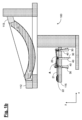
第1コンポーネント及び第2コンポーネントを、第1及び第2コンポーネント間の相対位置を変えることができる位置決め装置に導入するステップと、
第1及び第2コンポーネント間の距離が所定の接着隙間を規定する第1値を有する第1相対位置を較正するステップと、
第1及び第2コンポーネント間の距離が第1値より大きい第2値を有する第2相対位置を較正するステップと、
第1及び第2コンポーネントを相互に第1値より大きく離して第1コンポーネントに接着剤を塗布するステップと、
第1及び第2コンポーネント間に接着結合を形成しながら第1相対位置を設定するステップと
を含み、第1コンポーネントに接着剤を塗布するステップより前に、第1相対位置を較正するステップ及び第2相対位置を較正するステップの両方を実行する。
Claims (16)
- マイクロリソグラフィ用の第1コンポーネントと第2コンポーネントとを接着結合する方法であって、前記第2コンポーネントは光学素子である方法において、
a)前記第1コンポーネント及び前記第2コンポーネントを、第1及び第2コンポーネント間の相対位置を変えることができる位置決め装置(100)に導入するステップと、
b)第1及び第2コンポーネント間の距離が所定の接着時の接着隙間を規定する第1値を有する第1相対位置を較正するステップと、
c)第1及び第2コンポーネント間の距離が前記第1値より大きい第2値であって、前記第1及び第2コンポーネントの相対調整の開始位置を示す前記第2値を有する第2相対位置を較正するステップと、
d)第1及び第2コンポーネントを相互に前記第1値より大きく離して前記第1コンポーネントに接着剤(26)を塗布するステップと、
e)第1及び第2コンポーネント間に前記接着結合を形成しながら前記第1相対位置を設定するステップと
を含み、前記第1コンポーネントに前記接着剤(26)を塗布するステップより前に、前記第1相対位置を較正するステップ及び前記第2相対位置を較正するステップの両方を実行する方法。 - 請求項1に記載の方法において、前記第2相対位置を較正するステップは、前記第1コンポーネントの表面に一時的に接触させた較正素子(50、55)の位置の測定を含むことを特徴とする方法。
- 請求項2に記載の方法において、前記較正素子(50)は、前記第2コンポーネントの表面に対応する幾何学的形状を有することを特徴とする方法。
- 請求項1~3のいずれか1項に記載の方法において、前記第1及び/又は第2相対位置を較正するステップは、少なくとも1つの距離センサ、特に光学距離センサを用いて実行されることを特徴とする方法。
- 請求項1~4のいずれか1項に記載の方法において、前記第1及び/又は第2相対位置を較正するステップは、6自由度の前記第2コンポーネントの位置合わせを含むことを特徴とする方法。
- 請求項5に記載の方法において、前記第2コンポーネントの位置合わせは、前記位置決め装置にある少なくとも1つのメカニカルストップ(112、113)を用いて実行されることを特徴とする方法。
- 請求項1~6のいずれか1項に記載の方法において、前記第1及び/又は第2相対位置を較正するステップは、前記第1コンポーネントの横方向の位置合わせを含むことを特徴とする方法。
- 請求項7に記載の方法において、前記第1コンポーネントの横方向の位置合わせは、前記位置決め装置にある少なくとも1つのメカニカルストップ(24)を用いて実行されることを特徴とする方法。
- 請求項1~8のいずれか1項に記載の方法において、前記第1コンポーネントは複数の部分面を含み、前記接着剤の塗布中に、各部分面のエッジ領域で予想されるメニスカス形成を考慮して相互に異なる部分面で接着剤の計量を変えることを特徴とする方法。
- 請求項1~9のいずれか1項に記載の方法において、前記接着剤の塗布中に、前記接着結合後に達する終了位置で予想される第1及び第2コンポーネント間の角度位置を考慮して前記接着剤を位置決めすることを特徴とする方法。
- 請求項1~10のいずれか1項に記載の方法において、前記第1コンポーネントはアクチュエータ(20)であることを特徴とする方法。
- 請求項1~11のいずれか1項に記載の方法において、前記第2コンポーネントは光学素子(10)、特にミラー又はレンズ素子であることを特徴とする方法。
- 照明装置及び投影レンズを備えたマイクロリソグラフィ投影露光装置(700、800)を製造する方法であって、請求項1~12のいずれか1項に記載の方法を実行することにより前記照明装置及び/又は前記投影レンズの第1コンポーネントと第2コンポーネントとが接着結合される方法。
- 請求項13に記載の方法において、前記第1コンポーネントはアクチュエータ(20)であることを特徴とする方法。
- 請求項13又は14に記載の方法において、前記第2コンポーネントは光学素子(10)、特にミラー又はレンズ素子であることを特徴とする方法。
- 請求項1~12のいずれか1項に記載の方法を実行するよう構成されたことを特徴とする、マイクロリソグラフィ用の第1コンポーネントと第2コンポーネントとを接着結合する装置。
Applications Claiming Priority (3)
| Application Number | Priority Date | Filing Date | Title |
|---|---|---|---|
| DE102019209610.7A DE102019209610A1 (de) | 2019-07-01 | 2019-07-01 | Verfahren und Vorrichtung zum Herstellen einer Klebeverbindung zwischen einer ersten Komponente und einer zweiten Komponente |
| DE102019209610.7 | 2019-07-01 | ||
| PCT/EP2020/066079 WO2021001127A1 (en) | 2019-07-01 | 2020-06-10 | Method and device for producing an adhesive bond between a first component and a second component |
Publications (2)
| Publication Number | Publication Date |
|---|---|
| JP2022538302A JP2022538302A (ja) | 2022-09-01 |
| JP7546005B2 true JP7546005B2 (ja) | 2024-09-05 |
Family
ID=71670208
Family Applications (1)
| Application Number | Title | Priority Date | Filing Date |
|---|---|---|---|
| JP2021577433A Active JP7546005B2 (ja) | 2019-07-01 | 2020-06-10 | 第1コンポーネントと第2コンポーネントとを接着結合する方法及び装置 |
Country Status (6)
| Country | Link |
|---|---|
| US (1) | US12397510B2 (ja) |
| EP (1) | EP3994528B1 (ja) |
| JP (1) | JP7546005B2 (ja) |
| CN (1) | CN114072731B (ja) |
| DE (1) | DE102019209610A1 (ja) |
| WO (1) | WO2021001127A1 (ja) |
Families Citing this family (2)
| Publication number | Priority date | Publication date | Assignee | Title |
|---|---|---|---|---|
| DE102021205368A1 (de) * | 2021-05-27 | 2022-12-01 | Carl Zeiss Smt Gmbh | Komponente für eine Projektionsbelichtungsanlage für die Halbleiterlithografie und Verfahren zur Auslegung der Komponente |
| EP4123381A1 (en) * | 2022-01-26 | 2023-01-25 | Carl Zeiss SMT GmbH | Method and device for producing an adhesive bond between a first component and at least one second component for microlithography |
Citations (4)
| Publication number | Priority date | Publication date | Assignee | Title |
|---|---|---|---|---|
| JP2004347753A (ja) | 2003-05-21 | 2004-12-09 | Matsushita Electric Ind Co Ltd | 形状可変ミラー素子及び形状可変ミラー素子の製造方法並びに形状可変ミラーユニット並びに光ピックアップ |
| JP2007329475A (ja) | 2006-06-06 | 2007-12-20 | Asml Netherlands Bv | リソグラフィ装置およびデバイス製造方法 |
| JP2015127048A (ja) | 2013-11-27 | 2015-07-09 | 芝浦メカトロニクス株式会社 | 塗布装置、塗布方法、表示装置用部材の製造装置及び表示装置用部材の製造方法 |
| DE102016214481A1 (de) | 2016-08-04 | 2016-09-29 | Carl Zeiss Smt Gmbh | Klebeverfahren und werkzeug hierfür |
Family Cites Families (14)
| Publication number | Priority date | Publication date | Assignee | Title |
|---|---|---|---|---|
| GB2048509B (en) * | 1979-05-03 | 1983-02-23 | Ferranti Ltd | Bonding optical element to support |
| EP1725910A2 (en) * | 2004-02-25 | 2006-11-29 | Carl Zeiss SMT AG | Device consisting of at least one optical element |
| US20060192328A1 (en) * | 2004-12-16 | 2006-08-31 | Carl Zeiss Smt Ag | Composite body |
| WO2006073111A1 (ja) | 2005-01-05 | 2006-07-13 | Nippon Telegraph And Telephone Corporation | ミラー装置、ミラーアレイ、光スイッチ、ミラー装置の製造方法及びミラー基板の製造方法 |
| CN100451725C (zh) * | 2005-01-05 | 2009-01-14 | 日本电信电话株式会社 | 反射镜器件、反射镜阵列、光开关及其制造方法 |
| DE102006043185B4 (de) * | 2006-09-14 | 2010-05-20 | Fraunhofer-Gesellschaft zur Förderung der angewandten Forschung e.V. | Verfahren zum justierten Verbinden von Platten und nach diesem Verfahren hergestellte optische Baugruppe |
| FR2958415B1 (fr) * | 2010-04-06 | 2012-08-17 | Alpao | Miroir deformable a faible empreinte de collage et procede de fabrication d'un tel miroir |
| CN103140782B (zh) * | 2010-07-28 | 2018-11-27 | 卡尔蔡司Smt有限责任公司 | 分面反射镜装置 |
| DE102010041576B4 (de) | 2010-09-29 | 2015-02-26 | Carl Zeiss Smt Gmbh | Verfahren zum Verbinden von Körpern, Verbundkörper sowie dessen Verwendung |
| DE102014218969A1 (de) * | 2014-09-22 | 2016-04-28 | Carl Zeiss Smt Gmbh | Optische Anordnung einer mikrolithographischen Projektionsbelichtungsanlage |
| JP6128337B2 (ja) * | 2014-10-23 | 2017-05-17 | パナソニックIpマネジメント株式会社 | 半導体装置の製造方法及び製造装置 |
| DE102017216128A1 (de) * | 2017-09-13 | 2019-03-14 | Carl Zeiss Smt Gmbh | Verfahren zum Bearbeiten eines Werkstücks bei der Herstellung eines optischen Elements |
| DE102017219754A1 (de) * | 2017-11-07 | 2018-01-04 | Carl Zeiss Smt Gmbh | Optisches System und Lithographieanlage |
| DE102018201981A1 (de) * | 2018-02-08 | 2018-03-29 | Carl Zeiss Smt Gmbh | Optisches system, messmaschine oder lithographieanlage und verfahren |
-
2019
- 2019-07-01 DE DE102019209610.7A patent/DE102019209610A1/de not_active Ceased
-
2020
- 2020-06-10 WO PCT/EP2020/066079 patent/WO2021001127A1/en not_active Ceased
- 2020-06-10 CN CN202080047597.9A patent/CN114072731B/zh active Active
- 2020-06-10 JP JP2021577433A patent/JP7546005B2/ja active Active
- 2020-06-10 EP EP20742651.1A patent/EP3994528B1/en active Active
-
2021
- 2021-12-30 US US17/565,655 patent/US12397510B2/en active Active
Patent Citations (4)
| Publication number | Priority date | Publication date | Assignee | Title |
|---|---|---|---|---|
| JP2004347753A (ja) | 2003-05-21 | 2004-12-09 | Matsushita Electric Ind Co Ltd | 形状可変ミラー素子及び形状可変ミラー素子の製造方法並びに形状可変ミラーユニット並びに光ピックアップ |
| JP2007329475A (ja) | 2006-06-06 | 2007-12-20 | Asml Netherlands Bv | リソグラフィ装置およびデバイス製造方法 |
| JP2015127048A (ja) | 2013-11-27 | 2015-07-09 | 芝浦メカトロニクス株式会社 | 塗布装置、塗布方法、表示装置用部材の製造装置及び表示装置用部材の製造方法 |
| DE102016214481A1 (de) | 2016-08-04 | 2016-09-29 | Carl Zeiss Smt Gmbh | Klebeverfahren und werkzeug hierfür |
Also Published As
| Publication number | Publication date |
|---|---|
| EP3994528A1 (en) | 2022-05-11 |
| EP3994528C0 (en) | 2023-08-02 |
| US20220118715A1 (en) | 2022-04-21 |
| DE102019209610A1 (de) | 2021-01-07 |
| CN114072731A (zh) | 2022-02-18 |
| JP2022538302A (ja) | 2022-09-01 |
| WO2021001127A1 (en) | 2021-01-07 |
| US12397510B2 (en) | 2025-08-26 |
| CN114072731B (zh) | 2025-08-12 |
| EP3994528B1 (en) | 2023-08-02 |
Similar Documents
| Publication | Publication Date | Title |
|---|---|---|
| US7961294B2 (en) | Imaging device in a projection exposure facility | |
| US8659744B2 (en) | Method for correcting a lithography projection objective, and such a projection objective | |
| KR20180126101A (ko) | 조명광학계, 조명 광학 장치, 노광 장치, 및 디바이스 제조 방법 | |
| US7643150B2 (en) | Optical apparatus, exposure apparatus, and device manufacturing method | |
| JP7546005B2 (ja) | 第1コンポーネントと第2コンポーネントとを接着結合する方法及び装置 | |
| JPH1039208A (ja) | 投影光学系 | |
| JP2007013179A5 (ja) | ||
| JP5472101B2 (ja) | 露光装置及びデバイス製造方法 | |
| CN109416515B (zh) | 保持装置、投影光学系统、曝光装置及物品制造方法 | |
| KR100992302B1 (ko) | 광학계, 노광장치 및 디바이스 제조방법 | |
| JP4582306B2 (ja) | 光学系及び露光装置 | |
| JP3958261B2 (ja) | 光学系の調整方法 | |
| JP2005308629A (ja) | ミラーユニット及びそれの製造方法 | |
| JP2008112756A (ja) | 光学素子駆動装置及びその制御方法、露光装置、並びにデバイス製造方法 | |
| JP2006030021A (ja) | 位置検出装置及び位置検出方法 | |
| JPH0963923A (ja) | X線投影露光装置 | |
| JP5445905B2 (ja) | 位置合わせ方法及び装置、並びに露光方法及び装置 | |
| JP6226525B2 (ja) | 露光装置、露光方法、それらを用いたデバイスの製造方法 | |
| JP2007132981A (ja) | 対物光学系、収差測定装置、および露光装置 | |
| JP2003100606A (ja) | 波面収差測定装置、露光装置及びデバイスの製造方法 | |
| JP2022026158A (ja) | 調整方法、露光方法及び物品の製造方法 | |
| JP2010152096A (ja) | ミラー基板、ミラー、露光装置、デバイス製造方法、およびミラーの製造方法 | |
| JP2005228922A (ja) | 露光装置 | |
| JP2009026977A (ja) | 投影光学系及びそれを有する露光装置 | |
| JP2019184928A (ja) | 露光装置、および物品の製造方法 |
Legal Events
| Date | Code | Title | Description |
|---|---|---|---|
| A621 | Written request for application examination |
Free format text: JAPANESE INTERMEDIATE CODE: A621 Effective date: 20230609 |
|
| A977 | Report on retrieval |
Free format text: JAPANESE INTERMEDIATE CODE: A971007 Effective date: 20240229 |
|
| A131 | Notification of reasons for refusal |
Free format text: JAPANESE INTERMEDIATE CODE: A131 Effective date: 20240305 |
|
| A521 | Request for written amendment filed |
Free format text: JAPANESE INTERMEDIATE CODE: A523 Effective date: 20240513 |
|
| TRDD | Decision of grant or rejection written | ||
| A01 | Written decision to grant a patent or to grant a registration (utility model) |
Free format text: JAPANESE INTERMEDIATE CODE: A01 Effective date: 20240806 |
|
| A61 | First payment of annual fees (during grant procedure) |
Free format text: JAPANESE INTERMEDIATE CODE: A61 Effective date: 20240826 |
|
| R150 | Certificate of patent or registration of utility model |
Ref document number: 7546005 Country of ref document: JP Free format text: JAPANESE INTERMEDIATE CODE: R150 |