JP7521076B2 - 差動入力回路、エラーアンプ、スイッチング電源 - Google Patents
差動入力回路、エラーアンプ、スイッチング電源 Download PDFInfo
- Publication number
- JP7521076B2 JP7521076B2 JP2023106832A JP2023106832A JP7521076B2 JP 7521076 B2 JP7521076 B2 JP 7521076B2 JP 2023106832 A JP2023106832 A JP 2023106832A JP 2023106832 A JP2023106832 A JP 2023106832A JP 7521076 B2 JP7521076 B2 JP 7521076B2
- Authority
- JP
- Japan
- Prior art keywords
- signal
- differential input
- voltage
- current
- input stage
- Prior art date
- Legal status (The legal status is an assumption and is not a legal conclusion. Google has not performed a legal analysis and makes no representation as to the accuracy of the status listed.)
- Active
Links
- 230000004044 response Effects 0.000 claims description 12
- 238000012937 correction Methods 0.000 description 40
- 239000003990 capacitor Substances 0.000 description 32
- 238000010586 diagram Methods 0.000 description 32
- 230000001360 synchronised effect Effects 0.000 description 29
- 238000001514 detection method Methods 0.000 description 26
- 239000004065 semiconductor Substances 0.000 description 25
- 238000000034 method Methods 0.000 description 16
- 102000001301 EGF receptor Human genes 0.000 description 11
- 101000851181 Homo sapiens Epidermal growth factor receptor Proteins 0.000 description 11
- 230000015572 biosynthetic process Effects 0.000 description 10
- 238000003786 synthesis reaction Methods 0.000 description 10
- 230000007423 decrease Effects 0.000 description 8
- 230000010355 oscillation Effects 0.000 description 8
- 238000005070 sampling Methods 0.000 description 7
- 239000002131 composite material Substances 0.000 description 5
- 230000001052 transient effect Effects 0.000 description 5
- 230000007274 generation of a signal involved in cell-cell signaling Effects 0.000 description 4
- 101000851696 Homo sapiens Steroid hormone receptor ERR2 Proteins 0.000 description 3
- 102100036831 Steroid hormone receptor ERR2 Human genes 0.000 description 3
- 239000000872 buffer Substances 0.000 description 3
- 230000000052 comparative effect Effects 0.000 description 3
- 230000006872 improvement Effects 0.000 description 3
- 230000008569 process Effects 0.000 description 3
- 230000007704 transition Effects 0.000 description 3
- 230000006399 behavior Effects 0.000 description 2
- 230000003247 decreasing effect Effects 0.000 description 2
- 238000013461 design Methods 0.000 description 2
- 238000007599 discharging Methods 0.000 description 2
- 230000001771 impaired effect Effects 0.000 description 2
- 238000012986 modification Methods 0.000 description 2
- 230000004048 modification Effects 0.000 description 2
- 230000002265 prevention Effects 0.000 description 2
- 230000000630 rising effect Effects 0.000 description 2
- 230000003321 amplification Effects 0.000 description 1
- 238000013459 approach Methods 0.000 description 1
- 230000008859 change Effects 0.000 description 1
- 230000000295 complement effect Effects 0.000 description 1
- 230000003111 delayed effect Effects 0.000 description 1
- 230000005669 field effect Effects 0.000 description 1
- 229910044991 metal oxide Inorganic materials 0.000 description 1
- 150000004706 metal oxides Chemical class 0.000 description 1
- 238000003199 nucleic acid amplification method Methods 0.000 description 1
- 230000004043 responsiveness Effects 0.000 description 1
- 239000007787 solid Substances 0.000 description 1
- 238000011144 upstream manufacturing Methods 0.000 description 1
Images


Classifications
-
- H—ELECTRICITY
- H03—ELECTRONIC CIRCUITRY
- H03F—AMPLIFIERS
- H03F3/00—Amplifiers with only discharge tubes or only semiconductor devices as amplifying elements
- H03F3/20—Power amplifiers, e.g. Class B amplifiers, Class C amplifiers
- H03F3/21—Power amplifiers, e.g. Class B amplifiers, Class C amplifiers with semiconductor devices only
- H03F3/217—Class D power amplifiers; Switching amplifiers
- H03F3/2173—Class D power amplifiers; Switching amplifiers of the bridge type
-
- H—ELECTRICITY
- H02—GENERATION; CONVERSION OR DISTRIBUTION OF ELECTRIC POWER
- H02M—APPARATUS FOR CONVERSION BETWEEN AC AND AC, BETWEEN AC AND DC, OR BETWEEN DC AND DC, AND FOR USE WITH MAINS OR SIMILAR POWER SUPPLY SYSTEMS; CONVERSION OF DC OR AC INPUT POWER INTO SURGE OUTPUT POWER; CONTROL OR REGULATION THEREOF
- H02M3/00—Conversion of DC power input into DC power output
- H02M3/02—Conversion of DC power input into DC power output without intermediate conversion into AC
- H02M3/04—Conversion of DC power input into DC power output without intermediate conversion into AC by static converters
- H02M3/10—Conversion of DC power input into DC power output without intermediate conversion into AC by static converters using discharge tubes with control electrode or semiconductor devices with control electrode
- H02M3/145—Conversion of DC power input into DC power output without intermediate conversion into AC by static converters using discharge tubes with control electrode or semiconductor devices with control electrode using devices of a triode or transistor type requiring continuous application of a control signal
- H02M3/155—Conversion of DC power input into DC power output without intermediate conversion into AC by static converters using discharge tubes with control electrode or semiconductor devices with control electrode using devices of a triode or transistor type requiring continuous application of a control signal using semiconductor devices only
- H02M3/156—Conversion of DC power input into DC power output without intermediate conversion into AC by static converters using discharge tubes with control electrode or semiconductor devices with control electrode using devices of a triode or transistor type requiring continuous application of a control signal using semiconductor devices only with automatic control of output voltage or current, e.g. switching regulators
- H02M3/158—Conversion of DC power input into DC power output without intermediate conversion into AC by static converters using discharge tubes with control electrode or semiconductor devices with control electrode using devices of a triode or transistor type requiring continuous application of a control signal using semiconductor devices only with automatic control of output voltage or current, e.g. switching regulators including plural semiconductor devices as final control devices for a single load
-
- H—ELECTRICITY
- H03—ELECTRONIC CIRCUITRY
- H03F—AMPLIFIERS
- H03F1/00—Details of amplifiers with only discharge tubes, only semiconductor devices or only unspecified devices as amplifying elements
- H03F1/52—Circuit arrangements for protecting such amplifiers
- H03F1/523—Circuit arrangements for protecting such amplifiers for amplifiers using field-effect devices
-
- H—ELECTRICITY
- H03—ELECTRONIC CIRCUITRY
- H03F—AMPLIFIERS
- H03F3/00—Amplifiers with only discharge tubes or only semiconductor devices as amplifying elements
- H03F3/20—Power amplifiers, e.g. Class B amplifiers, Class C amplifiers
- H03F3/21—Power amplifiers, e.g. Class B amplifiers, Class C amplifiers with semiconductor devices only
- H03F3/217—Class D power amplifiers; Switching amplifiers
- H03F3/2171—Class D power amplifiers; Switching amplifiers with field-effect devices
-
- H—ELECTRICITY
- H03—ELECTRONIC CIRCUITRY
- H03F—AMPLIFIERS
- H03F3/00—Amplifiers with only discharge tubes or only semiconductor devices as amplifying elements
- H03F3/45—Differential amplifiers
- H03F3/45071—Differential amplifiers with semiconductor devices only
- H03F3/45076—Differential amplifiers with semiconductor devices only characterised by the way of implementation of the active amplifying circuit in the differential amplifier
- H03F3/45475—Differential amplifiers with semiconductor devices only characterised by the way of implementation of the active amplifying circuit in the differential amplifier using IC blocks as the active amplifying circuit
-
- H—ELECTRICITY
- H03—ELECTRONIC CIRCUITRY
- H03F—AMPLIFIERS
- H03F2200/00—Indexing scheme relating to amplifiers
- H03F2200/351—Pulse width modulation being used in an amplifying circuit
-
- H—ELECTRICITY
- H03—ELECTRONIC CIRCUITRY
- H03F—AMPLIFIERS
- H03F2203/00—Indexing scheme relating to amplifiers with only discharge tubes or only semiconductor devices as amplifying elements covered by H03F3/00
- H03F2203/45—Indexing scheme relating to differential amplifiers
- H03F2203/45726—Indexing scheme relating to differential amplifiers the LC comprising more than one switch, which are not cross coupled
-
- Y—GENERAL TAGGING OF NEW TECHNOLOGICAL DEVELOPMENTS; GENERAL TAGGING OF CROSS-SECTIONAL TECHNOLOGIES SPANNING OVER SEVERAL SECTIONS OF THE IPC; TECHNICAL SUBJECTS COVERED BY FORMER USPC CROSS-REFERENCE ART COLLECTIONS [XRACs] AND DIGESTS
- Y02—TECHNOLOGIES OR APPLICATIONS FOR MITIGATION OR ADAPTATION AGAINST CLIMATE CHANGE
- Y02B—CLIMATE CHANGE MITIGATION TECHNOLOGIES RELATED TO BUILDINGS, e.g. HOUSING, HOUSE APPLIANCES OR RELATED END-USER APPLICATIONS
- Y02B70/00—Technologies for an efficient end-user side electric power management and consumption
- Y02B70/10—Technologies improving the efficiency by using switched-mode power supplies [SMPS], i.e. efficient power electronics conversion e.g. power factor correction or reduction of losses in power supplies or efficient standby modes
Landscapes
- Engineering & Computer Science (AREA)
- Power Engineering (AREA)
- Dc-Dc Converters (AREA)
- Amplifiers (AREA)
- Measurement Of Velocity Or Position Using Acoustic Or Ultrasonic Waves (AREA)
Description
図1は、スイッチング電源の基本構成を示す図である。本構成例のスイッチング電源100は、入力電圧PVDDから出力電圧VOUTを生成して不図示の負荷に供給するPWM[pulse width modulation]駆動方式のDC/DCコンバータであり、スイッチング出力回路110と、帰還電圧生成回路120と、基準電圧生成回路130と、エラーアンプ140と、ランプ信号生成回路150と、オシレータ160と、PWMコンパレータ170と、制御回路180と、スイッチ駆動回路190と、を有する。
図2は、スイッチング電源100の第1実施形態を示す図である。本実施形態のスイッチング電源100は、電流モード制御方式の出力帰還制御を実現するための手段として、先出の構成要素(本図では、スイッチング出力回路110、エラーアンプ140、ランプ信号生成回路150、オシレータ160、PWMコンパレータ170、及び、制御回路180を明示)に加えて、下側電流検出部210と、情報合成部220と、情報保持部230をさらに有する。
図4は、スイッチング電源100の第2実施形態を示す図である。本実施形態のスイッチング電源100は、第1実施形態(図2)をベースとしつつ、サンプル/ホールド回路231及び232とランプ信号生成回路150の構成が具体化されている。
図6は、スイッチング電源100の第3実施形態を示す図である。本実施形態のスイッチング電源100は、先出の基本構成(図1)、ないしは、第1実施形態(図2)または第2実施形態(図4)をベースとしつつ、積分要素を持たないエラーアンプ140の入力誤差Vofs(=FB-REF)を検出してエラーアンプ140の入力信号(=帰還電圧FBと基準電圧REFの少なくとも一方)を補正する誤差補正部240をさらに有する。なお、誤差補正部240は、コンパレータ241とデジタル較正部242を含む。
図7は、スイッチング電源100の第4実施形態を示す図である。本実施形態のスイッチング電源100は、先出の第3実施形態(図6)と同じく、誤差補正部240を備えているが、その回路構成が異なっている。
図8は、スイッチング電源100の第5実施形態を示す図である。本実施形態のスイッチング電源100は、先の第3実施形態(図6)や第4実施形態(図7)と同じく、誤差補正部240を備えているが、その回路構成が異なっている。
図9は、スイッチング電源100の第6実施形態を示す図である。本実施形態のスイッチング電源100は、第1実施形態(図2)または第2実施形態(図4)をベースとしつつ、上側電流検出部250をさらに有する。
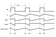
図12は、帰還端子T4がオープンしたときの挙動を示す図である。出力電圧VOUTの帰還経路が故障などにより切断された場合には、出力電圧VOUTの帰還入力を受け付けるための帰還端子T4がオープンとなる。
図13は、スイッチング電源100の第7実施形態を示す図である。本実施形態は、先の基本構成(図1)をベースとしつつ、オープン保護部600が追加されている。
図14は、スイッチング電源100の第8実施形態を示す図である。本実施形態は、先の第7実施形態(図13)をベースとしつつ、帰還電圧生成回路120の構成やプルアップ電流Ipの生成動作に新規な工夫がなされている。
図15は、スイッチング電源100の第9実施形態を示す図である。本実施形態は、先出の第7実施形態(図13)をベースとしつつ、帰還電圧生成回路120が割愛されており、帰還端子T4の端子電圧VT4(=帰還端子T4の非オープン時にはVT4=VOUT)がエラーアンプ140に直接入力されている。
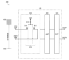
図16は、スイッチング電源100の第10実施形態(=後出の第12実施形態(図19)と対比される第1比較例に相当)を示す図である。本実施形態のスイッチング電源100において、エラーアンプ140は、差動入力回路300と、増幅回路400と、差動出力回路500と、を含む。
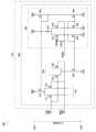
図17は、スイッチング電源100の第11実施形態(=後出の第12実施形態(図19)と対比される第2比較例に相当)を示す図である。本実施形態は、先の第10実施形態(図16)をベースとしつつ、差動入力回路300に改良が加えられている。そこで、本図では、増幅回路400や出力回路500の描写を割愛し、差動入力回路300についての重点的な説明を行う。
図19は、スイッチング電源100の第12実施形態を示す図である。本実施形態は、先の第11実施形態(図17)をベースとしつつ、差動入力回路300に更なる改良が加えられている。そこで、本図でも、増幅回路400や出力回路500の描写を割愛し、差動入力回路300についての重点的な説明を行う。
図21は、スイッチング電源100の第13実施形態(=後出の第14実施形態(図22及び図23)と対比される第3比較例に相当)を示す図である。本実施形態のスイッチング電源100において、エラーアンプ140は、差動入力回路300と、増幅回路400と、差動出力回路500と、を含む。
図22及び図23は、それぞれ、スイッチング電源100の第14実施形態を示す図である。本実施形態は、先出の第13実施形態(図21)をベースとしつつ、差動入力回路300に改良が加えられている。そこで、本図では、増幅回路400や出力回路500の描写を割愛し、差動入力回路300についての重点的な説明を行う。
図25は、スイッチング電源100の第15実施形態を示す図である。本実施形態は、先の第14実施形態(図22及び図23)をベースとしつつ、信号経路切替部360の一変形例として、信号経路切替部370が設けられている。そこで、本図でも、増幅回路400や出力回路500の描写を割愛し、差動入力回路300について重点的に説明する。
なお、これまでに説明してきた種々の実施形態は、矛盾のない限り、任意に組み合わせることが可能である。
また、これまでに説明してきたスイッチング電源100は、様々なアプリケーションの電源手段として利用することができる。なお、アプリケーションの一例としては、図26のテレビX、図27のパソコンY、及び、図28のスマートフォンZを挙げることができる。もちろん、ここに挙げた以外のアプリケーションにもスイッチング電源100を適用し得ることは言うまでもない。
以下では、本明細書中に開示されている種々の実施形態について総括的に述べる。
なお、本明細書中に開示されている種々の技術的特徴は、上記実施形態のほか、その技術的創作の主旨を逸脱しない範囲で種々の変更を加えることが可能である。すなわち、上記実施形態は、全ての点で例示であって制限的なものではないと考えられるべきであり、本発明の技術的範囲は、上記実施形態に限定されるものではなく、特許請求の範囲と均等の意味及び範囲内に属する全ての変更が含まれると理解されるべきである。
110 スイッチング出力回路
111 出力トランジスタ(PMOSFET)
112 同期整流トランジスタ(NMOSFET)
113 インダクタ
114 キャパシタ
120 帰還電圧生成回路
121、122 抵抗
123 キャパシタ
130 基準電圧生成回路
140 エラーアンプ
150 ランプ信号生成回路
151 電流源
160 オシレータ
170 PWMコンパレータ
180 制御回路
190 スイッチ駆動回路
191、192 ドライバ
200 半導体集積回路装置(電源制御IC)
210 下側電流検出部
211 スイッチ
212 抵抗
220 情報合成部
221、222 抵抗
230 情報保持部
231、232 サンプル/ホールド回路
240 誤差補正部
241 コンパレータ
242 デジタル較正部
243 誤差補正アンプ
244 キャパシタ
245 抵抗
246 デジタル較正部
247 誤差補正アンプ
250 上側電流検出部
251 電流源
300 差動入力回路
310 差動入力段(Pチャネル型)
311、312、314 PMOSFET
313 電流源
320 差動入力段(Nチャネル型)
321、322、324 NMOSFET
323 電流源
330 gm平坦化部
340 入力段切替部
341、342、343 PMOSFET
344、345、346 NMOSFET
347 電流源
348 インバータ
350 差動入力段
351、352 NMOSFET
353 電流源
360、370 信号経路切替部
371、372、373 スイッチ
374 インバータ
400 増幅回路
500 差動出力回路
600 オープン保護部
C1、C2 キャパシタ
SW1、SW2 スイッチ
T1、T2、T3、T4 外部端子
X テレビ
Y パソコン
Z スマートフォン
Claims (1)
- 入力電圧から出力電圧を生成するスイッチング出力回路と、
前記出力電圧と所定の基準電圧との差分に応じた誤差信号を生成するエラーアンプと、
前記誤差信号とランプ信号を比較してデューティ制御を行うPWMコンパレータと、
を有する、スイッチング電源であって、
前記エラーアンプは、分圧することなくそのまま入力される前記出力電圧と前記基準電圧とを差動入力信号として受け付ける差動入力回路を有し、
前記差動入力回路は、
一対のPチャネル型トランジスタで前記差動入力信号を受け付ける第1差動入力段と、
一対のNチャネル型トランジスタで前記差動入力信号を受け付ける第2差動入力段と、
前記第1差動入力段及び前記第2差動入力段双方の共通アクティブ領域を含む全ての動作領域で前記エラーアンプのトランスコンダクタンスをフラットに維持するように前記第1差動入力段及び前記第2差動入力段を択一的に動作させる入力段切替部と、
を有し、
前記入力段切替部は、前記差動入力信号が前記共通アクティブ領域に設定された所定の閾値レベルよりも低いときに前記第1差動入力段を動作させて前記第2差動入力段を停止させ、前記差動入力信号が前記閾値レベルよりも高いときに前記第2差動入力段を動作させて前記第1差動入力段を停止させ、
前記入力段切替部は、入力段切替信号に応じて前記第1差動入力段及び前記第2差動入力段の一方に駆動電流を供給し、
前記入力段切替部は、前記入力段切替信号及びその論理反転信号の入力を受け付ける差動対と、前記差動対に電流を供給する電流源と、を含み、前記差動対から出力される2系統の電流を前記第1差動入力段及び前記第2差動入力段それぞれの駆動電流として出力する、スイッチング電源。
Applications Claiming Priority (9)
| Application Number | Priority Date | Filing Date | Title |
|---|---|---|---|
| JP2018118506 | 2018-06-22 | ||
| JP2018118506 | 2018-06-22 | ||
| JP2018120560 | 2018-06-26 | ||
| JP2018120560 | 2018-06-26 | ||
| JP2018120564 | 2018-06-26 | ||
| JP2018120564 | 2018-06-26 | ||
| JP2020525227A JP7058326B2 (ja) | 2018-06-22 | 2018-12-18 | スイッチング電源、半導体集積回路装置、差動入力回路 |
| PCT/JP2018/046497 WO2019244374A1 (ja) | 2018-06-22 | 2018-12-18 | スイッチング電源、半導体集積回路装置、差動入力回路 |
| JP2022064998A JP7307229B2 (ja) | 2018-06-22 | 2022-04-11 | スイッチング電源、半導体集積回路装置 |
Related Parent Applications (1)
| Application Number | Title | Priority Date | Filing Date |
|---|---|---|---|
| JP2022064998A Division JP7307229B2 (ja) | 2018-06-22 | 2022-04-11 | スイッチング電源、半導体集積回路装置 |
Publications (2)
| Publication Number | Publication Date |
|---|---|
| JP2023134535A JP2023134535A (ja) | 2023-09-27 |
| JP7521076B2 true JP7521076B2 (ja) | 2024-07-23 |
Family
ID=68983709
Family Applications (3)
| Application Number | Title | Priority Date | Filing Date |
|---|---|---|---|
| JP2020525227A Active JP7058326B2 (ja) | 2018-06-22 | 2018-12-18 | スイッチング電源、半導体集積回路装置、差動入力回路 |
| JP2022064998A Active JP7307229B2 (ja) | 2018-06-22 | 2022-04-11 | スイッチング電源、半導体集積回路装置 |
| JP2023106832A Active JP7521076B2 (ja) | 2018-06-22 | 2023-06-29 | 差動入力回路、エラーアンプ、スイッチング電源 |
Family Applications Before (2)
| Application Number | Title | Priority Date | Filing Date |
|---|---|---|---|
| JP2020525227A Active JP7058326B2 (ja) | 2018-06-22 | 2018-12-18 | スイッチング電源、半導体集積回路装置、差動入力回路 |
| JP2022064998A Active JP7307229B2 (ja) | 2018-06-22 | 2022-04-11 | スイッチング電源、半導体集積回路装置 |
Country Status (4)
| Country | Link |
|---|---|
| US (3) | US11405008B2 (ja) |
| JP (3) | JP7058326B2 (ja) |
| DE (1) | DE112018007757T5 (ja) |
| WO (1) | WO2019244374A1 (ja) |
Families Citing this family (9)
| Publication number | Priority date | Publication date | Assignee | Title |
|---|---|---|---|---|
| US11405008B2 (en) | 2018-06-22 | 2022-08-02 | Rohm Co., Ltd. | Switching power supply, semiconductor integrated circuit device, and differential input circuit |
| US10784917B2 (en) * | 2018-11-27 | 2020-09-22 | Texas Instruments Incorporated | PSI5 base current sampling in synchronous mode |
| DE112020006170T5 (de) | 2019-12-17 | 2022-11-17 | Rohm Co., Ltd. | Ausgangsrückkopplungsregelkreis |
| JP7518896B2 (ja) * | 2020-03-17 | 2024-07-18 | ローム株式会社 | 出力帰還制御回路、スイッチング電源 |
| JP7352512B2 (ja) * | 2020-04-28 | 2023-09-28 | 日立Astemo株式会社 | 電源回路及び電子制御装置 |
| CN113759270B (zh) * | 2021-09-07 | 2023-12-29 | 上海集成电路研发中心有限公司 | 电源检测电路及集成电路芯片 |
| CN114221535B (zh) * | 2021-12-21 | 2023-12-19 | 阳光电源股份有限公司 | 一种车载充电器、dcdc变换器及控制方法 |
| US12323116B2 (en) * | 2022-04-29 | 2025-06-03 | Dialog Semiconductor (Uk) Limited | Broadband amplifier with DC gain error correction |
| US20250300560A1 (en) * | 2024-03-20 | 2025-09-25 | Texas Instruments Incorporated | Multiphase power converter with distributed control |
Citations (7)
| Publication number | Priority date | Publication date | Assignee | Title |
|---|---|---|---|---|
| JP2002043871A (ja) | 2000-07-31 | 2002-02-08 | Fujitsu Ltd | オペアンプ回路のバイアス電流制御方法、オペアンプ回路、電流制御回路、及び半導体装置 |
| JP2008311904A (ja) | 2007-06-14 | 2008-12-25 | Panasonic Corp | 演算増幅回路 |
| JP2011004309A (ja) | 2009-06-22 | 2011-01-06 | Renesas Electronics Corp | 差動信号受信回路および表示装置 |
| JP2011199973A (ja) | 2010-03-18 | 2011-10-06 | Panasonic Corp | スイッチングレギュレータ |
| JP2014204291A (ja) | 2013-04-04 | 2014-10-27 | 富士電機株式会社 | 演算増幅回路 |
| US20150326193A1 (en) | 2014-05-09 | 2015-11-12 | Analog Devices Global | Amplifier input stage and amplifier |
| WO2018030230A1 (ja) | 2016-08-10 | 2018-02-15 | ローム株式会社 | スイッチングレギュレータ及び集積回路パッケージ |
Family Cites Families (24)
| Publication number | Priority date | Publication date | Assignee | Title |
|---|---|---|---|---|
| JPS5954306A (ja) | 1982-09-22 | 1984-03-29 | Nippon Denso Co Ltd | 差動増幅器 |
| US6587670B1 (en) * | 1998-12-22 | 2003-07-01 | Harris Corporation | Dual mode class D amplifiers |
| US6300826B1 (en) * | 2000-05-05 | 2001-10-09 | Ericsson Telefon Ab L M | Apparatus and method for efficiently amplifying wideband envelope signals |
| US6605993B2 (en) | 2000-05-16 | 2003-08-12 | Fujitsu Limited | Operational amplifier circuit |
| US6316995B1 (en) * | 2000-06-02 | 2001-11-13 | National Semiconductor Corporation | Input stage for constant gm amplifier circuit and method |
| US6566961B2 (en) * | 2001-03-30 | 2003-05-20 | Institute Of Microelectronics | Wide-band single-ended to differential converter in CMOS technology |
| US6566951B1 (en) * | 2001-10-25 | 2003-05-20 | Lsi Logic Corporation | Low voltage variable gain amplifier having constant common mode DC output |
| US6518842B1 (en) * | 2002-06-07 | 2003-02-11 | Analog Devices, Inc. | Bipolar rail-to-rail input stage with selectable transition threshold |
| US6963244B1 (en) * | 2003-12-12 | 2005-11-08 | Analog Devices, Inc. | Common mode linearized input stage and amplifier topology |
| JP4423667B2 (ja) * | 2004-03-29 | 2010-03-03 | Tdkラムダ株式会社 | 電流帰還モジュール |
| US7514911B2 (en) | 2004-05-13 | 2009-04-07 | Marvell World Trade Ltd. | Voltage regulator feedback protection method and apparatus |
| JP2008043086A (ja) * | 2006-08-08 | 2008-02-21 | Toshiba Corp | 電源装置及びその制御方法 |
| JP2011072102A (ja) | 2009-09-25 | 2011-04-07 | Rohm Co Ltd | スイッチングレギュレータ |
| US8374012B2 (en) * | 2010-06-10 | 2013-02-12 | Carefusion 303, Inc. | Phase-controlled uninterruptible power supply |
| CN105450186B (zh) * | 2014-08-29 | 2019-04-19 | 意法半导体研发(深圳)有限公司 | 用于音频放大器的高级电流限制功能 |
| JP6307398B2 (ja) | 2014-09-24 | 2018-04-04 | ローム株式会社 | 電流モード制御型スイッチング電源装置 |
| US10076963B2 (en) | 2014-09-24 | 2018-09-18 | Rohm Co., Ltd. | Current mode control type switching power supply device |
| JP6457242B2 (ja) | 2014-11-04 | 2019-01-23 | ローム株式会社 | スイッチング電源装置 |
| JP2016181071A (ja) | 2015-03-24 | 2016-10-13 | 日立オートモティブシステムズ株式会社 | 電源装置 |
| JP6539534B2 (ja) | 2015-07-31 | 2019-07-03 | ローム株式会社 | 電源回路 |
| US9812962B2 (en) * | 2015-09-30 | 2017-11-07 | Intersil Americas LLC | Method and system for increasing efficiency and controlling slew rate in DC-DC converters |
| US10203708B2 (en) | 2015-11-30 | 2019-02-12 | Rohm Co., Ltd. | Power regulator to control output voltage using feedback |
| JP6791722B2 (ja) | 2015-11-30 | 2020-11-25 | ローム株式会社 | 電源レギュレータ |
| US11405008B2 (en) | 2018-06-22 | 2022-08-02 | Rohm Co., Ltd. | Switching power supply, semiconductor integrated circuit device, and differential input circuit |
-
2018
- 2018-12-18 US US17/056,314 patent/US11405008B2/en active Active
- 2018-12-18 JP JP2020525227A patent/JP7058326B2/ja active Active
- 2018-12-18 WO PCT/JP2018/046497 patent/WO2019244374A1/ja not_active Ceased
- 2018-12-18 DE DE112018007757.8T patent/DE112018007757T5/de active Pending
-
2022
- 2022-04-11 JP JP2022064998A patent/JP7307229B2/ja active Active
- 2022-04-21 US US17/725,860 patent/US11664775B2/en active Active
-
2023
- 2023-04-24 US US18/305,590 patent/US12047045B2/en active Active
- 2023-06-29 JP JP2023106832A patent/JP7521076B2/ja active Active
Patent Citations (7)
| Publication number | Priority date | Publication date | Assignee | Title |
|---|---|---|---|---|
| JP2002043871A (ja) | 2000-07-31 | 2002-02-08 | Fujitsu Ltd | オペアンプ回路のバイアス電流制御方法、オペアンプ回路、電流制御回路、及び半導体装置 |
| JP2008311904A (ja) | 2007-06-14 | 2008-12-25 | Panasonic Corp | 演算増幅回路 |
| JP2011004309A (ja) | 2009-06-22 | 2011-01-06 | Renesas Electronics Corp | 差動信号受信回路および表示装置 |
| JP2011199973A (ja) | 2010-03-18 | 2011-10-06 | Panasonic Corp | スイッチングレギュレータ |
| JP2014204291A (ja) | 2013-04-04 | 2014-10-27 | 富士電機株式会社 | 演算増幅回路 |
| US20150326193A1 (en) | 2014-05-09 | 2015-11-12 | Analog Devices Global | Amplifier input stage and amplifier |
| WO2018030230A1 (ja) | 2016-08-10 | 2018-02-15 | ローム株式会社 | スイッチングレギュレータ及び集積回路パッケージ |
Also Published As
| Publication number | Publication date |
|---|---|
| US20210257978A1 (en) | 2021-08-19 |
| US12047045B2 (en) | 2024-07-23 |
| JP2023134535A (ja) | 2023-09-27 |
| JP7058326B2 (ja) | 2022-04-21 |
| JP7307229B2 (ja) | 2023-07-11 |
| US11405008B2 (en) | 2022-08-02 |
| JP2022095857A (ja) | 2022-06-28 |
| WO2019244374A1 (ja) | 2019-12-26 |
| US11664775B2 (en) | 2023-05-30 |
| US20220247371A1 (en) | 2022-08-04 |
| DE112018007757T5 (de) | 2021-03-11 |
| US20230261625A1 (en) | 2023-08-17 |
| JPWO2019244374A1 (ja) | 2021-06-17 |
Similar Documents
| Publication | Publication Date | Title |
|---|---|---|
| JP7521076B2 (ja) | 差動入力回路、エラーアンプ、スイッチング電源 | |
| US10651846B2 (en) | Driver circuit and switching regulator | |
| JP3614156B2 (ja) | 電源回路 | |
| JP6212225B2 (ja) | 電力コンバータソフトスタート回路 | |
| US8686705B2 (en) | Current mode synchronous rectification DC/DC converter | |
| US20070296386A1 (en) | Switching power-supply circuit and semiconductor integrated circuit | |
| US8120338B2 (en) | Dropper-type regulator | |
| US8928302B2 (en) | Step-up/down type power supply circuit | |
| US20110080198A1 (en) | Charge pump circuit, and method of controlling charge pump circuit | |
| JP4610199B2 (ja) | Dc−dcコンバータ用半導体集積回路及びdc−dcコンバータ | |
| CN101247080A (zh) | 对电压转换器的自举电容充电的电路 | |
| WO2023219031A1 (ja) | ゲート駆動回路、パワーグッド回路、過電流検出回路、発振防止回路、スイッチング制御回路、および、スイッチング電源装置 | |
| US10468989B2 (en) | Switching regulator including a clamp circuit | |
| US10164531B2 (en) | Adaptive control method for generating non overlapping time in output devices | |
| US7583138B1 (en) | System and method for controlling an error amplifier between control mode changes | |
| JP2014057466A (ja) | スイッチングレギュレータ | |
| US8416591B2 (en) | DC-DC converter with soft start circuit | |
| JP7581239B2 (ja) | 出力帰還制御回路 | |
| US20200403506A1 (en) | High-efficiency pulse width modulation for switching power converters | |
| JP4311683B2 (ja) | 半導体装置、降圧チョッパレギュレータ、電子機器 | |
| US11271476B2 (en) | Power supply circuit comprising a charge pump circuit and a feedback circuit for the charge pump circuit | |
| US20250226751A1 (en) | Electric power supply control device and switching electric power supply | |
| US10566892B1 (en) | Power stage overdrive extender for area optimization and operation at low supply voltage | |
| JP5983446B2 (ja) | ゲート駆動回路およびスイッチング電源システム | |
| JP2008067531A (ja) | スイッチング制御回路 |
Legal Events
| Date | Code | Title | Description |
|---|---|---|---|
| A621 | Written request for application examination |
Free format text: JAPANESE INTERMEDIATE CODE: A621 Effective date: 20230629 |
|
| A977 | Report on retrieval |
Free format text: JAPANESE INTERMEDIATE CODE: A971007 Effective date: 20240221 |
|
| A131 | Notification of reasons for refusal |
Free format text: JAPANESE INTERMEDIATE CODE: A131 Effective date: 20240227 |
|
| A521 | Request for written amendment filed |
Free format text: JAPANESE INTERMEDIATE CODE: A523 Effective date: 20240403 |
|
| TRDD | Decision of grant or rejection written | ||
| A01 | Written decision to grant a patent or to grant a registration (utility model) |
Free format text: JAPANESE INTERMEDIATE CODE: A01 Effective date: 20240709 |
|
| A61 | First payment of annual fees (during grant procedure) |
Free format text: JAPANESE INTERMEDIATE CODE: A61 Effective date: 20240710 |
|
| R150 | Certificate of patent or registration of utility model |
Ref document number: 7521076 Country of ref document: JP Free format text: JAPANESE INTERMEDIATE CODE: R150 |