JP7471810B2 - リングアセンブリ、基板支持体及び基板処理装置 - Google Patents
リングアセンブリ、基板支持体及び基板処理装置 Download PDFInfo
- Publication number
- JP7471810B2 JP7471810B2 JP2019225271A JP2019225271A JP7471810B2 JP 7471810 B2 JP7471810 B2 JP 7471810B2 JP 2019225271 A JP2019225271 A JP 2019225271A JP 2019225271 A JP2019225271 A JP 2019225271A JP 7471810 B2 JP7471810 B2 JP 7471810B2
- Authority
- JP
- Japan
- Prior art keywords
- annular member
- edge ring
- disposed
- ring
- substrate
- Prior art date
- Legal status (The legal status is an assumption and is not a legal conclusion. Google has not performed a legal analysis and makes no representation as to the accuracy of the status listed.)
- Active
Links
Images


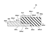
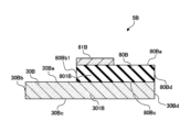

Classifications
-
- H—ELECTRICITY
- H01—ELECTRIC ELEMENTS
- H01J—ELECTRIC DISCHARGE TUBES OR DISCHARGE LAMPS
- H01J37/00—Discharge tubes with provision for introducing objects or material to be exposed to the discharge, e.g. for the purpose of examination or processing thereof
- H01J37/32—Gas-filled discharge tubes
- H01J37/32431—Constructional details of the reactor
- H01J37/32623—Mechanical discharge control means
- H01J37/32642—Focus rings
-
- H—ELECTRICITY
- H01—ELECTRIC ELEMENTS
- H01J—ELECTRIC DISCHARGE TUBES OR DISCHARGE LAMPS
- H01J37/00—Discharge tubes with provision for introducing objects or material to be exposed to the discharge, e.g. for the purpose of examination or processing thereof
- H01J37/32—Gas-filled discharge tubes
- H01J37/32431—Constructional details of the reactor
- H01J37/32715—Workpiece holder
-
- H—ELECTRICITY
- H10—SEMICONDUCTOR DEVICES; ELECTRIC SOLID-STATE DEVICES NOT OTHERWISE PROVIDED FOR
- H10P—GENERIC PROCESSES OR APPARATUS FOR THE MANUFACTURE OR TREATMENT OF DEVICES COVERED BY CLASS H10
- H10P72/00—Handling or holding of wafers, substrates or devices during manufacture or treatment thereof
- H10P72/04—Apparatus for manufacture or treatment
- H10P72/0402—Apparatus for fluid treatment
- H10P72/0418—Apparatus for fluid treatment for etching
- H10P72/0421—Apparatus for fluid treatment for etching for drying etching
-
- H—ELECTRICITY
- H10—SEMICONDUCTOR DEVICES; ELECTRIC SOLID-STATE DEVICES NOT OTHERWISE PROVIDED FOR
- H10P—GENERIC PROCESSES OR APPARATUS FOR THE MANUFACTURE OR TREATMENT OF DEVICES COVERED BY CLASS H10
- H10P72/00—Handling or holding of wafers, substrates or devices during manufacture or treatment thereof
- H10P72/04—Apparatus for manufacture or treatment
- H10P72/0431—Apparatus for thermal treatment
- H10P72/0434—Apparatus for thermal treatment mainly by convection
-
- H—ELECTRICITY
- H10—SEMICONDUCTOR DEVICES; ELECTRIC SOLID-STATE DEVICES NOT OTHERWISE PROVIDED FOR
- H10P—GENERIC PROCESSES OR APPARATUS FOR THE MANUFACTURE OR TREATMENT OF DEVICES COVERED BY CLASS H10
- H10P72/00—Handling or holding of wafers, substrates or devices during manufacture or treatment thereof
- H10P72/70—Handling or holding of wafers, substrates or devices during manufacture or treatment thereof for supporting or gripping
- H10P72/72—Handling or holding of wafers, substrates or devices during manufacture or treatment thereof for supporting or gripping using electrostatic chucks
-
- H—ELECTRICITY
- H01—ELECTRIC ELEMENTS
- H01J—ELECTRIC DISCHARGE TUBES OR DISCHARGE LAMPS
- H01J2237/00—Discharge tubes exposing object to beam, e.g. for analysis treatment, etching, imaging
- H01J2237/32—Processing objects by plasma generation
- H01J2237/33—Processing objects by plasma generation characterised by the type of processing
- H01J2237/332—Coating
- H01J2237/3321—CVD [Chemical Vapor Deposition]
-
- H—ELECTRICITY
- H01—ELECTRIC ELEMENTS
- H01J—ELECTRIC DISCHARGE TUBES OR DISCHARGE LAMPS
- H01J2237/00—Discharge tubes exposing object to beam, e.g. for analysis treatment, etching, imaging
- H01J2237/32—Processing objects by plasma generation
- H01J2237/33—Processing objects by plasma generation characterised by the type of processing
- H01J2237/334—Etching
- H01J2237/3341—Reactive etching
-
- H—ELECTRICITY
- H10—SEMICONDUCTOR DEVICES; ELECTRIC SOLID-STATE DEVICES NOT OTHERWISE PROVIDED FOR
- H10P—GENERIC PROCESSES OR APPARATUS FOR THE MANUFACTURE OR TREATMENT OF DEVICES COVERED BY CLASS H10
- H10P72/00—Handling or holding of wafers, substrates or devices during manufacture or treatment thereof
- H10P72/70—Handling or holding of wafers, substrates or devices during manufacture or treatment thereof for supporting or gripping
- H10P72/76—Handling or holding of wafers, substrates or devices during manufacture or treatment thereof for supporting or gripping using mechanical means, e.g. clamps or pinches
- H10P72/7604—Handling or holding of wafers, substrates or devices during manufacture or treatment thereof for supporting or gripping using mechanical means, e.g. clamps or pinches the wafers being placed on a susceptor, stage or support
- H10P72/7611—Handling or holding of wafers, substrates or devices during manufacture or treatment thereof for supporting or gripping using mechanical means, e.g. clamps or pinches the wafers being placed on a susceptor, stage or support characterised by edge profile or support profile
Landscapes
- Physics & Mathematics (AREA)
- Engineering & Computer Science (AREA)
- Plasma & Fusion (AREA)
- Chemical & Material Sciences (AREA)
- Analytical Chemistry (AREA)
- Drying Of Semiconductors (AREA)
- Plasma Technology (AREA)
- Chemical Vapour Deposition (AREA)
Priority Applications (3)
| Application Number | Priority Date | Filing Date | Title |
|---|---|---|---|
| JP2019225271A JP7471810B2 (ja) | 2019-12-13 | 2019-12-13 | リングアセンブリ、基板支持体及び基板処理装置 |
| KR1020200168167A KR20210075855A (ko) | 2019-12-13 | 2020-12-04 | 링 어셈블리, 기판 지지체 어셈블리 및 기판 처리 장치 |
| US17/117,177 US20210183629A1 (en) | 2019-12-13 | 2020-12-10 | Ring assembly, substrate support assembly and substrate processing apparatus |
Applications Claiming Priority (1)
| Application Number | Priority Date | Filing Date | Title |
|---|---|---|---|
| JP2019225271A JP7471810B2 (ja) | 2019-12-13 | 2019-12-13 | リングアセンブリ、基板支持体及び基板処理装置 |
Publications (3)
| Publication Number | Publication Date |
|---|---|
| JP2021097065A JP2021097065A (ja) | 2021-06-24 |
| JP2021097065A5 JP2021097065A5 (https=) | 2022-09-27 |
| JP7471810B2 true JP7471810B2 (ja) | 2024-04-22 |
Family
ID=76320649
Family Applications (1)
| Application Number | Title | Priority Date | Filing Date |
|---|---|---|---|
| JP2019225271A Active JP7471810B2 (ja) | 2019-12-13 | 2019-12-13 | リングアセンブリ、基板支持体及び基板処理装置 |
Country Status (3)
| Country | Link |
|---|---|
| US (1) | US20210183629A1 (https=) |
| JP (1) | JP7471810B2 (https=) |
| KR (1) | KR20210075855A (https=) |
Families Citing this family (1)
| Publication number | Priority date | Publication date | Assignee | Title |
|---|---|---|---|---|
| US12528652B2 (en) * | 2021-07-15 | 2026-01-20 | Kingtek Elec-Technology Co., Ltd. | Pre-jig wafer carrier disc installation/uninstallation device and method thereof |
Citations (6)
| Publication number | Priority date | Publication date | Assignee | Title |
|---|---|---|---|---|
| JP2005277369A (ja) | 2003-09-05 | 2005-10-06 | Tokyo Electron Ltd | フォーカスリング及びプラズマ処理装置 |
| JP2007515081A (ja) | 2003-12-17 | 2007-06-07 | ラム リサーチ コーポレーション | プラズマ反応器のエッチング速度ドリフトを低減するための温度制御されたホットエッジリングアセンブリ |
| JP2010027860A (ja) | 2008-07-18 | 2010-02-04 | Tokyo Electron Ltd | フォーカスリング及び基板載置台、並びにそれらを備えたプラズマ処理装置 |
| JP2013168690A (ja) | 2013-06-06 | 2013-08-29 | Tokyo Electron Ltd | プラズマ処理装置およびフォーカスリングとフォーカスリング部品 |
| JP2018032857A (ja) | 2016-08-23 | 2018-03-01 | アプライド マテリアルズ インコーポレイテッドApplied Materials,Incorporated | 半導体プロセスモジュールのためのエッジリングまたはプロセスキット |
| JP2019102521A (ja) | 2017-11-29 | 2019-06-24 | 東京エレクトロン株式会社 | 半導体製造装置用の部品及び半導体製造装置 |
Family Cites Families (4)
| Publication number | Priority date | Publication date | Assignee | Title |
|---|---|---|---|---|
| JPH08339895A (ja) * | 1995-06-12 | 1996-12-24 | Tokyo Electron Ltd | プラズマ処理装置 |
| JP3121524B2 (ja) * | 1995-06-07 | 2001-01-09 | 東京エレクトロン株式会社 | エッチング装置 |
| US6554954B2 (en) | 2001-04-03 | 2003-04-29 | Applied Materials Inc. | Conductive collar surrounding semiconductor workpiece in plasma chamber |
| JP2018129386A (ja) | 2017-02-08 | 2018-08-16 | 東京エレクトロン株式会社 | プラズマ処理装置 |
-
2019
- 2019-12-13 JP JP2019225271A patent/JP7471810B2/ja active Active
-
2020
- 2020-12-04 KR KR1020200168167A patent/KR20210075855A/ko not_active Ceased
- 2020-12-10 US US17/117,177 patent/US20210183629A1/en not_active Abandoned
Patent Citations (6)
| Publication number | Priority date | Publication date | Assignee | Title |
|---|---|---|---|---|
| JP2005277369A (ja) | 2003-09-05 | 2005-10-06 | Tokyo Electron Ltd | フォーカスリング及びプラズマ処理装置 |
| JP2007515081A (ja) | 2003-12-17 | 2007-06-07 | ラム リサーチ コーポレーション | プラズマ反応器のエッチング速度ドリフトを低減するための温度制御されたホットエッジリングアセンブリ |
| JP2010027860A (ja) | 2008-07-18 | 2010-02-04 | Tokyo Electron Ltd | フォーカスリング及び基板載置台、並びにそれらを備えたプラズマ処理装置 |
| JP2013168690A (ja) | 2013-06-06 | 2013-08-29 | Tokyo Electron Ltd | プラズマ処理装置およびフォーカスリングとフォーカスリング部品 |
| JP2018032857A (ja) | 2016-08-23 | 2018-03-01 | アプライド マテリアルズ インコーポレイテッドApplied Materials,Incorporated | 半導体プロセスモジュールのためのエッジリングまたはプロセスキット |
| JP2019102521A (ja) | 2017-11-29 | 2019-06-24 | 東京エレクトロン株式会社 | 半導体製造装置用の部品及び半導体製造装置 |
Also Published As
| Publication number | Publication date |
|---|---|
| KR20210075855A (ko) | 2021-06-23 |
| JP2021097065A (ja) | 2021-06-24 |
| US20210183629A1 (en) | 2021-06-17 |
Similar Documents
| Publication | Publication Date | Title |
|---|---|---|
| US11830751B2 (en) | Plasma processing apparatus and plasma processing method | |
| US11328904B2 (en) | Substrate processing apparatus | |
| JP6556046B2 (ja) | プラズマ処理方法およびプラズマ処理装置 | |
| JP7390880B2 (ja) | エッジリング及び基板処理装置 | |
| US10615008B2 (en) | Temperature control method | |
| JP6643950B2 (ja) | プラズマ処理方法 | |
| KR102241740B1 (ko) | 온도 제어 방법 및 플라즈마 처리 장치 | |
| JPH08335568A (ja) | エッチング装置 | |
| JP7175160B2 (ja) | 基板処理装置 | |
| US20220122820A1 (en) | Substrate processing apparatus | |
| KR102826843B1 (ko) | 기판 처리 장치 | |
| TWI789492B (zh) | 被處理體的載置裝置及處理裝置 | |
| KR20210125434A (ko) | 에지 링, 거치대 및 기판 처리 장치 | |
| JP7471810B2 (ja) | リングアセンブリ、基板支持体及び基板処理装置 | |
| JP4754609B2 (ja) | 処理装置およびそのクリーニング方法 | |
| JP7479236B2 (ja) | 基板処理装置 | |
| KR102037169B1 (ko) | 기판처리장치 | |
| JP7246451B2 (ja) | プラズマ処理装置及びプラズマ処理方法 | |
| JP7285152B2 (ja) | プラズマ処理装置 | |
| KR100510076B1 (ko) | 플라즈마 에칭 장치 | |
| JP2006253733A (ja) | プラズマ処理装置およびそのクリーニング方法 | |
| JP7605695B2 (ja) | エッジリング及びエッチング装置 | |
| KR101098793B1 (ko) | 대구경 웨이퍼 처리를 위한 적응형 플라즈마 소스 및 플라즈마 챔버 | |
| TW202234512A (zh) | 基板支持器、電漿處理系統及電漿蝕刻方法 |
Legal Events
| Date | Code | Title | Description |
|---|---|---|---|
| A521 | Request for written amendment filed |
Free format text: JAPANESE INTERMEDIATE CODE: A523 Effective date: 20220915 |
|
| A621 | Written request for application examination |
Free format text: JAPANESE INTERMEDIATE CODE: A621 Effective date: 20220915 |
|
| A131 | Notification of reasons for refusal |
Free format text: JAPANESE INTERMEDIATE CODE: A131 Effective date: 20230613 |
|
| A977 | Report on retrieval |
Free format text: JAPANESE INTERMEDIATE CODE: A971007 Effective date: 20230615 |
|
| A521 | Request for written amendment filed |
Free format text: JAPANESE INTERMEDIATE CODE: A523 Effective date: 20230726 |
|
| A131 | Notification of reasons for refusal |
Free format text: JAPANESE INTERMEDIATE CODE: A131 Effective date: 20231031 |
|
| TRDD | Decision of grant or rejection written | ||
| A01 | Written decision to grant a patent or to grant a registration (utility model) |
Free format text: JAPANESE INTERMEDIATE CODE: A01 Effective date: 20240312 |
|
| A61 | First payment of annual fees (during grant procedure) |
Free format text: JAPANESE INTERMEDIATE CODE: A61 Effective date: 20240410 |
|
| R150 | Certificate of patent or registration of utility model |
Ref document number: 7471810 Country of ref document: JP Free format text: JAPANESE INTERMEDIATE CODE: R150 |