JP7471810B2 - リングアセンブリ、基板支持体及び基板処理装置 - Google Patents
リングアセンブリ、基板支持体及び基板処理装置 Download PDFInfo
- Publication number
- JP7471810B2 JP7471810B2 JP2019225271A JP2019225271A JP7471810B2 JP 7471810 B2 JP7471810 B2 JP 7471810B2 JP 2019225271 A JP2019225271 A JP 2019225271A JP 2019225271 A JP2019225271 A JP 2019225271A JP 7471810 B2 JP7471810 B2 JP 7471810B2
- Authority
- JP
- Japan
- Prior art keywords
- annular member
- edge ring
- disposed
- ring
- substrate
- Prior art date
- Legal status (The legal status is an assumption and is not a legal conclusion. Google has not performed a legal analysis and makes no representation as to the accuracy of the status listed.)
- Active
Links
- 239000000758 substrate Substances 0.000 title claims description 76
- 229910052710 silicon Inorganic materials 0.000 claims description 5
- 239000010703 silicon Substances 0.000 claims description 5
- VYPSYNLAJGMNEJ-UHFFFAOYSA-N Silicium dioxide Chemical compound O=[Si]=O VYPSYNLAJGMNEJ-UHFFFAOYSA-N 0.000 claims description 4
- HBMJWWWQQXIZIP-UHFFFAOYSA-N silicon carbide Chemical compound [Si+]#[C-] HBMJWWWQQXIZIP-UHFFFAOYSA-N 0.000 claims description 4
- 229910052814 silicon oxide Inorganic materials 0.000 claims description 4
- 229910010271 silicon carbide Inorganic materials 0.000 claims 2
- 150000002500 ions Chemical class 0.000 description 12
- 230000002093 peripheral effect Effects 0.000 description 8
- 238000000034 method Methods 0.000 description 6
- 230000000052 comparative effect Effects 0.000 description 4
- XUIMIQQOPSSXEZ-UHFFFAOYSA-N Silicon Chemical compound [Si] XUIMIQQOPSSXEZ-UHFFFAOYSA-N 0.000 description 3
- 239000000463 material Substances 0.000 description 3
- 230000004048 modification Effects 0.000 description 3
- 238000012986 modification Methods 0.000 description 3
- 238000001020 plasma etching Methods 0.000 description 3
- 229910052782 aluminium Inorganic materials 0.000 description 2
- XAGFODPZIPBFFR-UHFFFAOYSA-N aluminium Chemical compound [Al] XAGFODPZIPBFFR-UHFFFAOYSA-N 0.000 description 2
- 239000004020 conductor Substances 0.000 description 2
- 230000000694 effects Effects 0.000 description 2
- 230000006870 function Effects 0.000 description 2
- 238000003860 storage Methods 0.000 description 2
- BSYNRYMUTXBXSQ-UHFFFAOYSA-N Aspirin Chemical compound CC(=O)OC1=CC=CC=C1C(O)=O BSYNRYMUTXBXSQ-UHFFFAOYSA-N 0.000 description 1
- 229910004298 SiO 2 Inorganic materials 0.000 description 1
- 238000005229 chemical vapour deposition Methods 0.000 description 1
- 239000003989 dielectric material Substances 0.000 description 1
- 238000001312 dry etching Methods 0.000 description 1
- 238000007688 edging Methods 0.000 description 1
- 238000005530 etching Methods 0.000 description 1
- -1 for example Inorganic materials 0.000 description 1
- 238000009616 inductively coupled plasma Methods 0.000 description 1
- 239000011810 insulating material Substances 0.000 description 1
- 238000004519 manufacturing process Methods 0.000 description 1
- 229910052751 metal Inorganic materials 0.000 description 1
- 239000002184 metal Substances 0.000 description 1
- 238000005268 plasma chemical vapour deposition Methods 0.000 description 1
- 239000003507 refrigerant Substances 0.000 description 1
- 239000004065 semiconductor Substances 0.000 description 1
- 229910001220 stainless steel Inorganic materials 0.000 description 1
- 239000010935 stainless steel Substances 0.000 description 1
Images


Classifications
-
- H—ELECTRICITY
- H01—ELECTRIC ELEMENTS
- H01J—ELECTRIC DISCHARGE TUBES OR DISCHARGE LAMPS
- H01J37/00—Discharge tubes with provision for introducing objects or material to be exposed to the discharge, e.g. for the purpose of examination or processing thereof
- H01J37/32—Gas-filled discharge tubes
- H01J37/32431—Constructional details of the reactor
- H01J37/32623—Mechanical discharge control means
- H01J37/32642—Focus rings
-
- H—ELECTRICITY
- H01—ELECTRIC ELEMENTS
- H01J—ELECTRIC DISCHARGE TUBES OR DISCHARGE LAMPS
- H01J37/00—Discharge tubes with provision for introducing objects or material to be exposed to the discharge, e.g. for the purpose of examination or processing thereof
- H01J37/32—Gas-filled discharge tubes
- H01J37/32431—Constructional details of the reactor
- H01J37/32715—Workpiece holder
-
- H—ELECTRICITY
- H01—ELECTRIC ELEMENTS
- H01L—SEMICONDUCTOR DEVICES NOT COVERED BY CLASS H10
- H01L21/00—Processes or apparatus adapted for the manufacture or treatment of semiconductor or solid state devices or of parts thereof
- H01L21/67—Apparatus specially adapted for handling semiconductor or electric solid state devices during manufacture or treatment thereof; Apparatus specially adapted for handling wafers during manufacture or treatment of semiconductor or electric solid state devices or components ; Apparatus not specifically provided for elsewhere
- H01L21/67005—Apparatus not specifically provided for elsewhere
- H01L21/67011—Apparatus for manufacture or treatment
- H01L21/67017—Apparatus for fluid treatment
- H01L21/67063—Apparatus for fluid treatment for etching
- H01L21/67069—Apparatus for fluid treatment for etching for drying etching
-
- H—ELECTRICITY
- H01—ELECTRIC ELEMENTS
- H01L—SEMICONDUCTOR DEVICES NOT COVERED BY CLASS H10
- H01L21/00—Processes or apparatus adapted for the manufacture or treatment of semiconductor or solid state devices or of parts thereof
- H01L21/67—Apparatus specially adapted for handling semiconductor or electric solid state devices during manufacture or treatment thereof; Apparatus specially adapted for handling wafers during manufacture or treatment of semiconductor or electric solid state devices or components ; Apparatus not specifically provided for elsewhere
- H01L21/67005—Apparatus not specifically provided for elsewhere
- H01L21/67011—Apparatus for manufacture or treatment
- H01L21/67098—Apparatus for thermal treatment
- H01L21/67109—Apparatus for thermal treatment mainly by convection
-
- H—ELECTRICITY
- H01—ELECTRIC ELEMENTS
- H01L—SEMICONDUCTOR DEVICES NOT COVERED BY CLASS H10
- H01L21/00—Processes or apparatus adapted for the manufacture or treatment of semiconductor or solid state devices or of parts thereof
- H01L21/67—Apparatus specially adapted for handling semiconductor or electric solid state devices during manufacture or treatment thereof; Apparatus specially adapted for handling wafers during manufacture or treatment of semiconductor or electric solid state devices or components ; Apparatus not specifically provided for elsewhere
- H01L21/683—Apparatus specially adapted for handling semiconductor or electric solid state devices during manufacture or treatment thereof; Apparatus specially adapted for handling wafers during manufacture or treatment of semiconductor or electric solid state devices or components ; Apparatus not specifically provided for elsewhere for supporting or gripping
- H01L21/6831—Apparatus specially adapted for handling semiconductor or electric solid state devices during manufacture or treatment thereof; Apparatus specially adapted for handling wafers during manufacture or treatment of semiconductor or electric solid state devices or components ; Apparatus not specifically provided for elsewhere for supporting or gripping using electrostatic chucks
-
- H—ELECTRICITY
- H01—ELECTRIC ELEMENTS
- H01L—SEMICONDUCTOR DEVICES NOT COVERED BY CLASS H10
- H01L21/00—Processes or apparatus adapted for the manufacture or treatment of semiconductor or solid state devices or of parts thereof
- H01L21/67—Apparatus specially adapted for handling semiconductor or electric solid state devices during manufacture or treatment thereof; Apparatus specially adapted for handling wafers during manufacture or treatment of semiconductor or electric solid state devices or components ; Apparatus not specifically provided for elsewhere
- H01L21/683—Apparatus specially adapted for handling semiconductor or electric solid state devices during manufacture or treatment thereof; Apparatus specially adapted for handling wafers during manufacture or treatment of semiconductor or electric solid state devices or components ; Apparatus not specifically provided for elsewhere for supporting or gripping
- H01L21/687—Apparatus specially adapted for handling semiconductor or electric solid state devices during manufacture or treatment thereof; Apparatus specially adapted for handling wafers during manufacture or treatment of semiconductor or electric solid state devices or components ; Apparatus not specifically provided for elsewhere for supporting or gripping using mechanical means, e.g. chucks, clamps or pinches
- H01L21/68714—Apparatus specially adapted for handling semiconductor or electric solid state devices during manufacture or treatment thereof; Apparatus specially adapted for handling wafers during manufacture or treatment of semiconductor or electric solid state devices or components ; Apparatus not specifically provided for elsewhere for supporting or gripping using mechanical means, e.g. chucks, clamps or pinches the wafers being placed on a susceptor, stage or support
- H01L21/68735—Apparatus specially adapted for handling semiconductor or electric solid state devices during manufacture or treatment thereof; Apparatus specially adapted for handling wafers during manufacture or treatment of semiconductor or electric solid state devices or components ; Apparatus not specifically provided for elsewhere for supporting or gripping using mechanical means, e.g. chucks, clamps or pinches the wafers being placed on a susceptor, stage or support characterised by edge profile or support profile
-
- H—ELECTRICITY
- H01—ELECTRIC ELEMENTS
- H01J—ELECTRIC DISCHARGE TUBES OR DISCHARGE LAMPS
- H01J2237/00—Discharge tubes exposing object to beam, e.g. for analysis treatment, etching, imaging
- H01J2237/32—Processing objects by plasma generation
- H01J2237/33—Processing objects by plasma generation characterised by the type of processing
- H01J2237/332—Coating
- H01J2237/3321—CVD [Chemical Vapor Deposition]
-
- H—ELECTRICITY
- H01—ELECTRIC ELEMENTS
- H01J—ELECTRIC DISCHARGE TUBES OR DISCHARGE LAMPS
- H01J2237/00—Discharge tubes exposing object to beam, e.g. for analysis treatment, etching, imaging
- H01J2237/32—Processing objects by plasma generation
- H01J2237/33—Processing objects by plasma generation characterised by the type of processing
- H01J2237/334—Etching
- H01J2237/3341—Reactive etching
Landscapes
- Engineering & Computer Science (AREA)
- Physics & Mathematics (AREA)
- Plasma & Fusion (AREA)
- Chemical & Material Sciences (AREA)
- Analytical Chemistry (AREA)
- General Physics & Mathematics (AREA)
- Condensed Matter Physics & Semiconductors (AREA)
- Manufacturing & Machinery (AREA)
- Computer Hardware Design (AREA)
- Microelectronics & Electronic Packaging (AREA)
- Power Engineering (AREA)
- Drying Of Semiconductors (AREA)
- Plasma Technology (AREA)
- Chemical Vapour Deposition (AREA)
Description
まず、図1を参照しながら基板処理装置1の全体構成の一例について説明する。図1は、本実施形態に係る基板処理装置1の概略構成を示す断面図である。なお、本実施形態では、基板処理装置1がRIE(Reactive Ion Etching)型の基板処理装置である例について説明する。ただし、基板処理装置1は、プラズマエッチング装置やプラズマCVD(Chemical Vapor Deposition)装置等であってもよい。
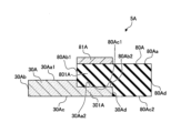
本実施形態のリングアセンブリ5について、詳細を説明する。図2は、本実施形態に係るリングアセンブリ5の断面図である。
図2に示すように、エッジリング30の外周部301の上面30aは、環状部材80により覆われている。つまり、環状部材80は、エッジリング30の上に内周部801が配置される。エッジリング30が他の部材によって覆われていない場合、内周面30b側に比べて外周面30d側が特に消耗がはやい。本実施形態のリングアセンブリ5では、エッジリング30の外周面30d側(外周部301)が環状部材80で覆われている。それによって、エッジリング30の外周面30d側(外周部301)の消耗を抑制することができる。
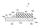
図3は、本実施形態に係るリングアセンブリ5の変形例であるリングアセンブリ5Aの断面図である。
図4は、本実施形態に係るリングアセンブリ5の変形例であるリングアセンブリ5Bの断面図である。
本実施形態の導電性部材81は、円環状の形状であったが、形状はそれに限らない。例えば、イオンの入射角や環状部材80の消耗度合いに応じて、円周方向の一部にたとえば円弧状の導電性部材81を設けてもよい。また、導電性部材81の内周面80b1側の端部からの径方向の寸法を長さLについても、環状部材80の消耗状況から、消耗している部分を覆うように定めてもよい。また、エッジリング30と環状部材80は、それぞれ一体の部材である場合に限らず、複数の部材で構成するようにしてもよい。
2 処理容器
5、5A、5B リングアセンブリ
6 基板支持体
10 載置台
25 静電チャック
30、30A、30B エッジリング
80、80A、80B 環状部材
80a 上面
801、801A 内周部
81、81A、81B 導電性部材
W 基板
Claims (20)
- 導電性のエッジリングと、
前記エッジリングの上に少なくとも内周部が配置される絶縁性の環状部材と、
上面視で前記エッジリングにオーバーラップする前記環状部材の上面の少なくとも一部に配置される導電性部材と、を備え、
前記環状部材の内径は、前記エッジリングの内径よりも大きく、
前記環状部材は、前記内周部の外側に配置され、前記内周部の厚さより厚い外周部を有する、
リングアセンブリ。 - 導電性のエッジリングと、
前記エッジリングの上に少なくとも内周部が配置される絶縁性の環状部材と、
上面視で前記エッジリングにオーバーラップする前記環状部材の上面の少なくとも一部に配置される導電性部材と、を備え、
前記導電性部材の内径は、前記環状部材の内径と等しく、
前記環状部材は、前記内周部の外側に配置され、前記内周部の厚さより厚い外周部を有する、
リングアセンブリ。 - 導電性のエッジリングと、
前記エッジリングの上に少なくとも内周部が配置される絶縁性の環状部材と、
上面視で前記エッジリングにオーバーラップする前記環状部材の上面の少なくとも一部に配置される導電性部材と、を備え、
前記導電性部材の外径は、前記環状部材の外径よりも小さく、
前記環状部材は、前記内周部の外側に配置され、前記内周部の厚さより厚い外周部を有する、
リングアセンブリ。 - 前記エッジリングは、ケイ素または炭化ケイ素で形成されている、
請求項1~3のいずれか一項に記載のリングアセンブリ。 - 前記環状部材は、酸化ケイ素で形成されている、
請求項1~4のいずれか一項に記載のリングアセンブリ。 - 前記導電性部材は、ケイ素または炭化ケイ素で形成されている、
請求項1~5のいずれか一項に記載のリングアセンブリ。 - 前記導電性部材は、環状又は円弧状である、
請求項1~6のいずれか一項に記載のリングアセンブリ。 - 前記導電性部材は、上面視で前記エッジリングにオーバーラップする前記環状部材の上面を覆う、
請求項1~7のいずれか一項に記載のリングアセンブリ。 - 前記導電性部材は、上面視で前記エッジリングにオーバーラップする前記環状部材の上面を内径側から所定の範囲覆う、
請求項1~7のいずれか一項に記載のリングアセンブリ。 - 前記導電性部材は、前記内周部に配置される、
請求項1~9のいずれか一項に記載のリングアセンブリ。 - 前記導電性部材の径方向の長さは、前記環状部材における前記エッジリングと重なる部分の径方向の長さに対して半分以上である、
請求項1~10のいずれか一項に記載のリングアセンブリ。 - 前記導電性部材の径方向の長さは、前記環状部材における前記エッジリングと重なる部分の径方向の長さに等しい、
請求項1~11のいずれか一項に記載のリングアセンブリ。 - 前記導電性部材は、前記内周部より薄い、
請求項1~12のいずれか一項に記載のリングアセンブリ。 - 前記導電性部材は、前記エッジリングより薄い、
請求項1~13のいずれか一項に記載のリングアセンブリ。 - 基板を載置する載置台と、
リングアセンブリと、を備え、
前記リングアセンブリは、
前記載置台の外周に載置され、基板を囲む導電性のエッジリングと、
前記エッジリングの上に少なくとも内周部が配置される絶縁性の環状部材と、
上面視で前記エッジリングにオーバーラップする前記環状部材の上面の少なくとも一部に配置される導電性部材と、を備え、
前記環状部材の内径は、前記エッジリングの内径よりも大きく、
前記環状部材は、前記内周部の外側に配置され、前記内周部の厚さより厚い外周部を有する、
基板支持体。 - 基板を載置する載置台と、
リングアセンブリと、を備え、
前記リングアセンブリは、
前記載置台の外周に載置され、基板を囲む導電性のエッジリングと、
前記エッジリングの上に少なくとも内周部が配置される絶縁性の環状部材と、
上面視で前記エッジリングにオーバーラップする前記環状部材の上面の少なくとも一部に配置される導電性部材と、を備え、
前記導電性部材の内径は、前記環状部材の内径と等しく、
前記環状部材は、前記内周部の外側に配置され、前記内周部の厚さより厚い外周部を有する、
基板支持体。 - 基板を載置する載置台と、
リングアセンブリと、を備え、
前記リングアセンブリは、
前記載置台の外周に載置され、基板を囲む導電性のエッジリングと、
前記エッジリングの上に少なくとも内周部が配置される絶縁性の環状部材と、
上面視で前記エッジリングにオーバーラップする前記環状部材の上面の少なくとも一部に配置される導電性部材と、を備え、
前記導電性部材の外径は、前記環状部材の外径よりも小さく、
前記環状部材は、前記内周部の外側に配置され、前記内周部の厚さより厚い外周部を有する、
基板支持体。 - チャンバと、基板支持体とを有する基板処理装置であって、
前記基板支持体は、
基板を載置する載置台と、
リングアセンブリと、を備え、
前記リングアセンブリは、
前記載置台の外周に載置され、基板を囲む導電性のエッジリングと、
前記エッジリングの上に少なくとも内周部が配置される絶縁性の環状部材と、
上面視で前記エッジリングにオーバーラップする前記環状部材の上面の少なくとも一部に配置される導電性部材と、を備え、
前記環状部材の内径は、前記エッジリングの内径よりも大きく、
前記環状部材は、前記内周部の外側に配置され、前記内周部の厚さより厚い外周部を有する、
基板処理装置。 - チャンバと、基板支持体とを有する基板処理装置であって、
前記基板支持体は、
基板を載置する載置台と、
リングアセンブリと、を備え、
前記リングアセンブリは、
前記載置台の外周に載置され、基板を囲む導電性のエッジリングと、
前記エッジリングの上に少なくとも内周部が配置される絶縁性の環状部材と、
上面視で前記エッジリングにオーバーラップする前記環状部材の上面の少なくとも一部に配置される導電性部材と、を備え、
前記導電性部材の内径は、前記環状部材の内径と等しく、
前記環状部材は、前記内周部の外側に配置され、前記内周部の厚さより厚い外周部を有する、
基板処理装置。 - チャンバと、基板支持体とを有する基板処理装置であって、
前記基板支持体は、
基板を載置する載置台と、
リングアセンブリと、を備え、
前記リングアセンブリは、
前記載置台の外周に載置され、基板を囲む導電性のエッジリングと、
前記エッジリングの上に少なくとも内周部が配置される絶縁性の環状部材と、
上面視で前記エッジリングにオーバーラップする前記環状部材の上面の少なくとも一部に配置される導電性部材と、を備え、
前記導電性部材の外径は、前記環状部材の外径よりも小さく、
前記環状部材は、前記内周部の外側に配置され、前記内周部の厚さより厚い外周部を有する、
基板処理装置。
Priority Applications (3)
| Application Number | Priority Date | Filing Date | Title |
|---|---|---|---|
| JP2019225271A JP7471810B2 (ja) | 2019-12-13 | 2019-12-13 | リングアセンブリ、基板支持体及び基板処理装置 |
| KR1020200168167A KR20210075855A (ko) | 2019-12-13 | 2020-12-04 | 링 어셈블리, 기판 지지체 어셈블리 및 기판 처리 장치 |
| US17/117,177 US20210183629A1 (en) | 2019-12-13 | 2020-12-10 | Ring assembly, substrate support assembly and substrate processing apparatus |
Applications Claiming Priority (1)
| Application Number | Priority Date | Filing Date | Title |
|---|---|---|---|
| JP2019225271A JP7471810B2 (ja) | 2019-12-13 | 2019-12-13 | リングアセンブリ、基板支持体及び基板処理装置 |
Publications (3)
| Publication Number | Publication Date |
|---|---|
| JP2021097065A JP2021097065A (ja) | 2021-06-24 |
| JP2021097065A5 JP2021097065A5 (ja) | 2022-09-27 |
| JP7471810B2 true JP7471810B2 (ja) | 2024-04-22 |
Family
ID=76320649
Family Applications (1)
| Application Number | Title | Priority Date | Filing Date |
|---|---|---|---|
| JP2019225271A Active JP7471810B2 (ja) | 2019-12-13 | 2019-12-13 | リングアセンブリ、基板支持体及び基板処理装置 |
Country Status (3)
| Country | Link |
|---|---|
| US (1) | US20210183629A1 (ja) |
| JP (1) | JP7471810B2 (ja) |
| KR (1) | KR20210075855A (ja) |
Citations (6)
| Publication number | Priority date | Publication date | Assignee | Title |
|---|---|---|---|---|
| JP2005277369A (ja) | 2003-09-05 | 2005-10-06 | Tokyo Electron Ltd | フォーカスリング及びプラズマ処理装置 |
| JP2007515081A (ja) | 2003-12-17 | 2007-06-07 | ラム リサーチ コーポレーション | プラズマ反応器のエッチング速度ドリフトを低減するための温度制御されたホットエッジリングアセンブリ |
| JP2010027860A (ja) | 2008-07-18 | 2010-02-04 | Tokyo Electron Ltd | フォーカスリング及び基板載置台、並びにそれらを備えたプラズマ処理装置 |
| JP2013168690A (ja) | 2013-06-06 | 2013-08-29 | Tokyo Electron Ltd | プラズマ処理装置およびフォーカスリングとフォーカスリング部品 |
| JP2018032857A (ja) | 2016-08-23 | 2018-03-01 | アプライド マテリアルズ インコーポレイテッドApplied Materials,Incorporated | 半導体プロセスモジュールのためのエッジリングまたはプロセスキット |
| JP2019102521A (ja) | 2017-11-29 | 2019-06-24 | 東京エレクトロン株式会社 | 半導体製造装置用の部品及び半導体製造装置 |
Family Cites Families (3)
| Publication number | Priority date | Publication date | Assignee | Title |
|---|---|---|---|---|
| JPH08339895A (ja) * | 1995-06-12 | 1996-12-24 | Tokyo Electron Ltd | プラズマ処理装置 |
| US6554954B2 (en) | 2001-04-03 | 2003-04-29 | Applied Materials Inc. | Conductive collar surrounding semiconductor workpiece in plasma chamber |
| JP2018129386A (ja) | 2017-02-08 | 2018-08-16 | 東京エレクトロン株式会社 | プラズマ処理装置 |
-
2019
- 2019-12-13 JP JP2019225271A patent/JP7471810B2/ja active Active
-
2020
- 2020-12-04 KR KR1020200168167A patent/KR20210075855A/ko active Search and Examination
- 2020-12-10 US US17/117,177 patent/US20210183629A1/en not_active Abandoned
Patent Citations (6)
| Publication number | Priority date | Publication date | Assignee | Title |
|---|---|---|---|---|
| JP2005277369A (ja) | 2003-09-05 | 2005-10-06 | Tokyo Electron Ltd | フォーカスリング及びプラズマ処理装置 |
| JP2007515081A (ja) | 2003-12-17 | 2007-06-07 | ラム リサーチ コーポレーション | プラズマ反応器のエッチング速度ドリフトを低減するための温度制御されたホットエッジリングアセンブリ |
| JP2010027860A (ja) | 2008-07-18 | 2010-02-04 | Tokyo Electron Ltd | フォーカスリング及び基板載置台、並びにそれらを備えたプラズマ処理装置 |
| JP2013168690A (ja) | 2013-06-06 | 2013-08-29 | Tokyo Electron Ltd | プラズマ処理装置およびフォーカスリングとフォーカスリング部品 |
| JP2018032857A (ja) | 2016-08-23 | 2018-03-01 | アプライド マテリアルズ インコーポレイテッドApplied Materials,Incorporated | 半導体プロセスモジュールのためのエッジリングまたはプロセスキット |
| JP2019102521A (ja) | 2017-11-29 | 2019-06-24 | 東京エレクトロン株式会社 | 半導体製造装置用の部品及び半導体製造装置 |
Also Published As
| Publication number | Publication date |
|---|---|
| JP2021097065A (ja) | 2021-06-24 |
| KR20210075855A (ko) | 2021-06-23 |
| US20210183629A1 (en) | 2021-06-17 |
Similar Documents
| Publication | Publication Date | Title |
|---|---|---|
| US20200321195A1 (en) | Substrate Processing Apparatus | |
| JP6556046B2 (ja) | プラズマ処理方法およびプラズマ処理装置 | |
| KR102614244B1 (ko) | 플라즈마 처리 장치 및 플라즈마 처리 방법 | |
| US10615008B2 (en) | Temperature control method | |
| KR102350148B1 (ko) | 플라즈마 처리 방법 | |
| KR102241740B1 (ko) | 온도 제어 방법 및 플라즈마 처리 장치 | |
| JPH08335568A (ja) | エッチング装置 | |
| US11398397B2 (en) | Electrostatic chuck and plasma processing apparatus including the same | |
| TWI789492B (zh) | 被處理體的載置裝置及處理裝置 | |
| JP7471810B2 (ja) | リングアセンブリ、基板支持体及び基板処理装置 | |
| KR102037169B1 (ko) | 기판처리장치 | |
| JP7175160B2 (ja) | 基板処理装置 | |
| JP4754609B2 (ja) | 処理装置およびそのクリーニング方法 | |
| JP7246451B2 (ja) | プラズマ処理装置及びプラズマ処理方法 | |
| JP2006310883A (ja) | プラズマ処理装置およびそのクリーニング方法 | |
| JP7390880B2 (ja) | エッジリング及び基板処理装置 | |
| US20220122820A1 (en) | Substrate processing apparatus | |
| JP7285152B2 (ja) | プラズマ処理装置 | |
| JP2006253733A (ja) | プラズマ処理装置およびそのクリーニング方法 | |
| JP7479236B2 (ja) | 基板処理装置 | |
| KR100510076B1 (ko) | 플라즈마 에칭 장치 | |
| US20210319987A1 (en) | Edge ring, stage and substrate processing apparatus | |
| US20210020408A1 (en) | Substrate support assembly, substrate processing apparatus, and edge ring | |
| KR101098793B1 (ko) | 대구경 웨이퍼 처리를 위한 적응형 플라즈마 소스 및 플라즈마 챔버 | |
| TW202234512A (zh) | 基板支持器、電漿處理系統及電漿蝕刻方法 |
Legal Events
| Date | Code | Title | Description |
|---|---|---|---|
| A521 | Request for written amendment filed |
Free format text: JAPANESE INTERMEDIATE CODE: A523 Effective date: 20220915 |
|
| A621 | Written request for application examination |
Free format text: JAPANESE INTERMEDIATE CODE: A621 Effective date: 20220915 |
|
| A131 | Notification of reasons for refusal |
Free format text: JAPANESE INTERMEDIATE CODE: A131 Effective date: 20230613 |
|
| A977 | Report on retrieval |
Free format text: JAPANESE INTERMEDIATE CODE: A971007 Effective date: 20230615 |
|
| A521 | Request for written amendment filed |
Free format text: JAPANESE INTERMEDIATE CODE: A523 Effective date: 20230726 |
|
| A131 | Notification of reasons for refusal |
Free format text: JAPANESE INTERMEDIATE CODE: A131 Effective date: 20231031 |
|
| TRDD | Decision of grant or rejection written | ||
| A01 | Written decision to grant a patent or to grant a registration (utility model) |
Free format text: JAPANESE INTERMEDIATE CODE: A01 Effective date: 20240312 |
|
| A61 | First payment of annual fees (during grant procedure) |
Free format text: JAPANESE INTERMEDIATE CODE: A61 Effective date: 20240410 |
|
| R150 | Certificate of patent or registration of utility model |
Ref document number: 7471810 Country of ref document: JP Free format text: JAPANESE INTERMEDIATE CODE: R150 |