JP7366025B2 - Printed wiring board and method for manufacturing printed wiring board - Google Patents
Printed wiring board and method for manufacturing printed wiring board Download PDFInfo
- Publication number
- JP7366025B2 JP7366025B2 JP2020533519A JP2020533519A JP7366025B2 JP 7366025 B2 JP7366025 B2 JP 7366025B2 JP 2020533519 A JP2020533519 A JP 2020533519A JP 2020533519 A JP2020533519 A JP 2020533519A JP 7366025 B2 JP7366025 B2 JP 7366025B2
- Authority
- JP
- Japan
- Prior art keywords
- printed wiring
- filling
- wiring board
- hole
- insulating layer
- Prior art date
- Legal status (The legal status is an assumption and is not a legal conclusion. Google has not performed a legal analysis and makes no representation as to the accuracy of the status listed.)
- Active
Links
- 238000004519 manufacturing process Methods 0.000 title claims description 53
- 238000000034 method Methods 0.000 title claims description 53
- 239000000758 substrate Substances 0.000 claims description 40
- RYGMFSIKBFXOCR-UHFFFAOYSA-N Copper Chemical compound [Cu] RYGMFSIKBFXOCR-UHFFFAOYSA-N 0.000 claims description 33
- 239000004020 conductor Substances 0.000 claims description 19
- 229910052802 copper Inorganic materials 0.000 claims description 16
- 239000010949 copper Substances 0.000 claims description 16
- 239000000463 material Substances 0.000 claims description 12
- 229920001343 polytetrafluoroethylene Polymers 0.000 claims description 12
- 239000004810 polytetrafluoroethylene Substances 0.000 claims description 12
- 238000005530 etching Methods 0.000 claims description 11
- 238000010030 laminating Methods 0.000 claims description 4
- QUQFTIVBFKLPCL-UHFFFAOYSA-L copper;2-amino-3-[(2-amino-2-carboxylatoethyl)disulfanyl]propanoate Chemical compound [Cu+2].[O-]C(=O)C(N)CSSCC(N)C([O-])=O QUQFTIVBFKLPCL-UHFFFAOYSA-L 0.000 claims description 3
- -1 polytetrafluoroethylene Polymers 0.000 claims description 3
- 230000000149 penetrating effect Effects 0.000 claims description 2
- 239000010410 layer Substances 0.000 description 95
- 238000010586 diagram Methods 0.000 description 26
- 239000011889 copper foil Substances 0.000 description 17
- 238000007747 plating Methods 0.000 description 10
- 229920005989 resin Polymers 0.000 description 8
- 239000011347 resin Substances 0.000 description 8
- 230000015572 biosynthetic process Effects 0.000 description 7
- 238000004891 communication Methods 0.000 description 5
- 230000000694 effects Effects 0.000 description 5
- 238000003475 lamination Methods 0.000 description 5
- 238000005429 filling process Methods 0.000 description 4
- 238000009413 insulation Methods 0.000 description 4
- 239000002344 surface layer Substances 0.000 description 3
- XLYOFNOQVPJJNP-UHFFFAOYSA-N water Substances O XLYOFNOQVPJJNP-UHFFFAOYSA-N 0.000 description 3
- 239000007864 aqueous solution Substances 0.000 description 2
- 239000011810 insulating material Substances 0.000 description 2
- 238000003754 machining Methods 0.000 description 2
- 230000005856 abnormality Effects 0.000 description 1
- 238000010521 absorption reaction Methods 0.000 description 1
- 239000002253 acid Substances 0.000 description 1
- 239000000654 additive Substances 0.000 description 1
- 230000000996 additive effect Effects 0.000 description 1
- 230000005540 biological transmission Effects 0.000 description 1
- 238000010276 construction Methods 0.000 description 1
- 238000009713 electroplating Methods 0.000 description 1
- 239000003822 epoxy resin Substances 0.000 description 1
- 239000011521 glass Substances 0.000 description 1
- 239000003365 glass fiber Substances 0.000 description 1
- 239000007788 liquid Substances 0.000 description 1
- 238000012986 modification Methods 0.000 description 1
- 230000004048 modification Effects 0.000 description 1
- 238000009832 plasma treatment Methods 0.000 description 1
- 229920000647 polyepoxide Polymers 0.000 description 1
- 238000000926 separation method Methods 0.000 description 1
- 239000000243 solution Substances 0.000 description 1
- 239000002759 woven fabric Substances 0.000 description 1
Images


Classifications
-
- H—ELECTRICITY
- H05—ELECTRIC TECHNIQUES NOT OTHERWISE PROVIDED FOR
- H05K—PRINTED CIRCUITS; CASINGS OR CONSTRUCTIONAL DETAILS OF ELECTRIC APPARATUS; MANUFACTURE OF ASSEMBLAGES OF ELECTRICAL COMPONENTS
- H05K1/00—Printed circuits
- H05K1/02—Details
- H05K1/11—Printed elements for providing electric connections to or between printed circuits
- H05K1/115—Via connections; Lands around holes or via connections
-
- H—ELECTRICITY
- H05—ELECTRIC TECHNIQUES NOT OTHERWISE PROVIDED FOR
- H05K—PRINTED CIRCUITS; CASINGS OR CONSTRUCTIONAL DETAILS OF ELECTRIC APPARATUS; MANUFACTURE OF ASSEMBLAGES OF ELECTRICAL COMPONENTS
- H05K3/00—Apparatus or processes for manufacturing printed circuits
- H05K3/40—Forming printed elements for providing electric connections to or between printed circuits
- H05K3/4038—Through-connections; Vertical interconnect access [VIA] connections
- H05K3/4053—Through-connections; Vertical interconnect access [VIA] connections by thick-film techniques
- H05K3/4069—Through-connections; Vertical interconnect access [VIA] connections by thick-film techniques for via connections in organic insulating substrates
-
- H—ELECTRICITY
- H05—ELECTRIC TECHNIQUES NOT OTHERWISE PROVIDED FOR
- H05K—PRINTED CIRCUITS; CASINGS OR CONSTRUCTIONAL DETAILS OF ELECTRIC APPARATUS; MANUFACTURE OF ASSEMBLAGES OF ELECTRICAL COMPONENTS
- H05K3/00—Apparatus or processes for manufacturing printed circuits
- H05K3/40—Forming printed elements for providing electric connections to or between printed circuits
- H05K3/42—Plated through-holes or plated via connections
- H05K3/421—Blind plated via connections
-
- H—ELECTRICITY
- H05—ELECTRIC TECHNIQUES NOT OTHERWISE PROVIDED FOR
- H05K—PRINTED CIRCUITS; CASINGS OR CONSTRUCTIONAL DETAILS OF ELECTRIC APPARATUS; MANUFACTURE OF ASSEMBLAGES OF ELECTRICAL COMPONENTS
- H05K3/00—Apparatus or processes for manufacturing printed circuits
- H05K3/40—Forming printed elements for providing electric connections to or between printed circuits
- H05K3/42—Plated through-holes or plated via connections
- H05K3/425—Plated through-holes or plated via connections characterised by the sequence of steps for plating the through-holes or via connections in relation to the conductive pattern
- H05K3/427—Plated through-holes or plated via connections characterised by the sequence of steps for plating the through-holes or via connections in relation to the conductive pattern initial plating of through-holes in metal-clad substrates
-
- H—ELECTRICITY
- H05—ELECTRIC TECHNIQUES NOT OTHERWISE PROVIDED FOR
- H05K—PRINTED CIRCUITS; CASINGS OR CONSTRUCTIONAL DETAILS OF ELECTRIC APPARATUS; MANUFACTURE OF ASSEMBLAGES OF ELECTRICAL COMPONENTS
- H05K3/00—Apparatus or processes for manufacturing printed circuits
- H05K3/46—Manufacturing multilayer circuits
- H05K3/4611—Manufacturing multilayer circuits by laminating two or more circuit boards
- H05K3/4623—Manufacturing multilayer circuits by laminating two or more circuit boards the circuit boards having internal via connections between two or more circuit layers before lamination, e.g. double-sided circuit boards
-
- H—ELECTRICITY
- H05—ELECTRIC TECHNIQUES NOT OTHERWISE PROVIDED FOR
- H05K—PRINTED CIRCUITS; CASINGS OR CONSTRUCTIONAL DETAILS OF ELECTRIC APPARATUS; MANUFACTURE OF ASSEMBLAGES OF ELECTRICAL COMPONENTS
- H05K3/00—Apparatus or processes for manufacturing printed circuits
- H05K3/46—Manufacturing multilayer circuits
- H05K3/4611—Manufacturing multilayer circuits by laminating two or more circuit boards
- H05K3/4626—Manufacturing multilayer circuits by laminating two or more circuit boards characterised by the insulating layers or materials
- H05K3/4635—Manufacturing multilayer circuits by laminating two or more circuit boards characterised by the insulating layers or materials laminating flexible circuit boards using additional insulating adhesive materials between the boards
-
- H—ELECTRICITY
- H05—ELECTRIC TECHNIQUES NOT OTHERWISE PROVIDED FOR
- H05K—PRINTED CIRCUITS; CASINGS OR CONSTRUCTIONAL DETAILS OF ELECTRIC APPARATUS; MANUFACTURE OF ASSEMBLAGES OF ELECTRICAL COMPONENTS
- H05K1/00—Printed circuits
- H05K1/02—Details
- H05K1/03—Use of materials for the substrate
- H05K1/0313—Organic insulating material
- H05K1/032—Organic insulating material consisting of one material
- H05K1/034—Organic insulating material consisting of one material containing halogen
-
- H—ELECTRICITY
- H05—ELECTRIC TECHNIQUES NOT OTHERWISE PROVIDED FOR
- H05K—PRINTED CIRCUITS; CASINGS OR CONSTRUCTIONAL DETAILS OF ELECTRIC APPARATUS; MANUFACTURE OF ASSEMBLAGES OF ELECTRICAL COMPONENTS
- H05K2201/00—Indexing scheme relating to printed circuits covered by H05K1/00
- H05K2201/01—Dielectrics
- H05K2201/0137—Materials
- H05K2201/015—Fluoropolymer, e.g. polytetrafluoroethylene [PTFE]
-
- H—ELECTRICITY
- H05—ELECTRIC TECHNIQUES NOT OTHERWISE PROVIDED FOR
- H05K—PRINTED CIRCUITS; CASINGS OR CONSTRUCTIONAL DETAILS OF ELECTRIC APPARATUS; MANUFACTURE OF ASSEMBLAGES OF ELECTRICAL COMPONENTS
- H05K2201/00—Indexing scheme relating to printed circuits covered by H05K1/00
- H05K2201/09—Shape and layout
- H05K2201/09209—Shape and layout details of conductors
- H05K2201/095—Conductive through-holes or vias
- H05K2201/09509—Blind vias, i.e. vias having one side closed
- H05K2201/09527—Inverse blind vias, i.e. bottoms outwards in multilayer PCB; Blind vias in centre of PCB having opposed bottoms
-
- H—ELECTRICITY
- H05—ELECTRIC TECHNIQUES NOT OTHERWISE PROVIDED FOR
- H05K—PRINTED CIRCUITS; CASINGS OR CONSTRUCTIONAL DETAILS OF ELECTRIC APPARATUS; MANUFACTURE OF ASSEMBLAGES OF ELECTRICAL COMPONENTS
- H05K2201/00—Indexing scheme relating to printed circuits covered by H05K1/00
- H05K2201/09—Shape and layout
- H05K2201/09209—Shape and layout details of conductors
- H05K2201/095—Conductive through-holes or vias
- H05K2201/09563—Metal filled via
-
- H—ELECTRICITY
- H05—ELECTRIC TECHNIQUES NOT OTHERWISE PROVIDED FOR
- H05K—PRINTED CIRCUITS; CASINGS OR CONSTRUCTIONAL DETAILS OF ELECTRIC APPARATUS; MANUFACTURE OF ASSEMBLAGES OF ELECTRICAL COMPONENTS
- H05K2201/00—Indexing scheme relating to printed circuits covered by H05K1/00
- H05K2201/09—Shape and layout
- H05K2201/09818—Shape or layout details not covered by a single group of H05K2201/09009 - H05K2201/09809
- H05K2201/09827—Tapered, e.g. tapered hole, via or groove
-
- H—ELECTRICITY
- H05—ELECTRIC TECHNIQUES NOT OTHERWISE PROVIDED FOR
- H05K—PRINTED CIRCUITS; CASINGS OR CONSTRUCTIONAL DETAILS OF ELECTRIC APPARATUS; MANUFACTURE OF ASSEMBLAGES OF ELECTRICAL COMPONENTS
- H05K2203/00—Indexing scheme relating to apparatus or processes for manufacturing printed circuits covered by H05K3/00
- H05K2203/06—Lamination
- H05K2203/061—Lamination of previously made multilayered subassemblies
-
- H—ELECTRICITY
- H05—ELECTRIC TECHNIQUES NOT OTHERWISE PROVIDED FOR
- H05K—PRINTED CIRCUITS; CASINGS OR CONSTRUCTIONAL DETAILS OF ELECTRIC APPARATUS; MANUFACTURE OF ASSEMBLAGES OF ELECTRICAL COMPONENTS
- H05K2203/00—Indexing scheme relating to apparatus or processes for manufacturing printed circuits covered by H05K3/00
- H05K2203/07—Treatments involving liquids, e.g. plating, rinsing
- H05K2203/0703—Plating
- H05K2203/0723—Electroplating, e.g. finish plating
-
- H—ELECTRICITY
- H05—ELECTRIC TECHNIQUES NOT OTHERWISE PROVIDED FOR
- H05K—PRINTED CIRCUITS; CASINGS OR CONSTRUCTIONAL DETAILS OF ELECTRIC APPARATUS; MANUFACTURE OF ASSEMBLAGES OF ELECTRICAL COMPONENTS
- H05K3/00—Apparatus or processes for manufacturing printed circuits
- H05K3/0011—Working of insulating substrates or insulating layers
- H05K3/0017—Etching of the substrate by chemical or physical means
- H05K3/002—Etching of the substrate by chemical or physical means by liquid chemical etching
-
- H—ELECTRICITY
- H05—ELECTRIC TECHNIQUES NOT OTHERWISE PROVIDED FOR
- H05K—PRINTED CIRCUITS; CASINGS OR CONSTRUCTIONAL DETAILS OF ELECTRIC APPARATUS; MANUFACTURE OF ASSEMBLAGES OF ELECTRICAL COMPONENTS
- H05K3/00—Apparatus or processes for manufacturing printed circuits
- H05K3/0011—Working of insulating substrates or insulating layers
- H05K3/0017—Etching of the substrate by chemical or physical means
- H05K3/0026—Etching of the substrate by chemical or physical means by laser ablation
- H05K3/0032—Etching of the substrate by chemical or physical means by laser ablation of organic insulating material
- H05K3/0035—Etching of the substrate by chemical or physical means by laser ablation of organic insulating material of blind holes, i.e. having a metal layer at the bottom
-
- H—ELECTRICITY
- H05—ELECTRIC TECHNIQUES NOT OTHERWISE PROVIDED FOR
- H05K—PRINTED CIRCUITS; CASINGS OR CONSTRUCTIONAL DETAILS OF ELECTRIC APPARATUS; MANUFACTURE OF ASSEMBLAGES OF ELECTRICAL COMPONENTS
- H05K3/00—Apparatus or processes for manufacturing printed circuits
- H05K3/0011—Working of insulating substrates or insulating layers
- H05K3/0055—After-treatment, e.g. cleaning or desmearing of holes
Landscapes
- Engineering & Computer Science (AREA)
- Microelectronics & Electronic Packaging (AREA)
- Manufacturing & Machinery (AREA)
- Printing Elements For Providing Electric Connections Between Printed Circuits (AREA)
- Production Of Multi-Layered Print Wiring Board (AREA)
Description
本開示は、印刷配線板及び印刷配線板の製造方法に関する。 The present disclosure relates to a printed wiring board and a method of manufacturing the printed wiring board.
複数の基板が積層された印刷配線板を製造する際に、各層の配線を導通させるためのビアとして、フィルドビアを形成することがある。
フィルドビアを有する印刷配線板の製造方法としては、例えば特許文献1が提案されている。
その具体的な内容は、以下である。
まず、仮基板の表面に樹脂層を分離可能に形成する。次に、レーザ加工により樹脂層にビア下穴を形成する。次に、ビア下穴内にスミア(樹脂残渣)を残した状態で樹脂層表面及びビア下穴内面にシード層を形成する。次に、電解めっきによりビア下穴内に配線層を形成する。次に、樹脂層を仮基板から分離し、樹脂層の仮基板と接していた面に露出するスミアを除去する。When manufacturing a printed wiring board in which a plurality of substrates are laminated, filled vias are sometimes formed as vias for electrically connecting wiring in each layer.
For example,
The specific contents are as follows.
First, a resin layer is separably formed on the surface of a temporary substrate. Next, a via pilot hole is formed in the resin layer by laser processing. Next, a seed layer is formed on the surface of the resin layer and the inner surface of the via pilot hole while leaving a smear (resin residue) in the via pilot hole. Next, a wiring layer is formed in the via pilot hole by electrolytic plating. Next, the resin layer is separated from the temporary substrate, and the smear exposed on the surface of the resin layer that was in contact with the temporary substrate is removed.
本開示の印刷配線板は、
平板状で厚さ方向に貫通する孔を有する第一絶縁層を備えた第一基板と、電解めっき銅で前記孔の中を充填するビアと、を備えた印刷配線板である。
前記ビアは、少なくとも前記孔の中の中心部を前記電解めっき銅で充填する第一充填部と、前記孔の中の前記第一充填部によって充填されていない領域を前記電解めっき銅で充填する第二充填部と、を有している。
前記第二充填部と前記第一充填部との間に存在する界面、又は前記第二充填部及び前記第一絶縁層と前記第一充填部との間に存在する界面は、前記第一絶縁層の厚さ方向一端にある第一面から前記第一絶縁層における前記第一面の裏面となる第二面へ向かうに従って細くなるよう傾斜する錐体面と、前記第二面と平行かつ前記第二面よりも前記第一面側へ位置する上底面と、を有する円錐台状である。
前記第一充填部は、その一部が前記第一面よりも前記孔の外側へ出て、前記第一面において前記孔の周囲に位置する第一ランド部と一体であり、前記第二充填部は、その一部が前記第二面よりも前記孔の外側へ出て、前記第二面において前記孔の周囲に位置する第二ランド部と一体である。
The printed wiring board of the present disclosure includes:
The printed wiring board includes a first substrate including a first insulating layer that is flat and has a hole penetrating through the thickness, and a via that fills the hole with electroplated copper .
The via includes a first filling portion that fills at least a central portion of the hole with the electrolytically plated copper , and a region of the hole that is not filled by the first filling portion that is filled with the electrolytically plated copper. It has a second filling part.
The interface existing between the second filling part and the first filling part, or the interface existing between the second filling part and the first insulating layer and the first filling part, a conical surface that is inclined to become narrower as it goes from a first surface at one end in the thickness direction of the layer to a second surface that is the back surface of the first surface in the first insulating layer; The upper base surface is located closer to the first surface than the second surface, and has a truncated conical shape.
A portion of the first filling portion protrudes outside the hole from the first surface, and is integral with a first land portion located around the hole on the first surface, and the second filling portion is integral with a first land portion located around the hole on the first surface. A portion of the land portion extends outside the hole beyond the second surface, and is integral with a second land portion located around the hole on the second surface.
また、本開示の印刷配線板の製造方法は、
平板状に形成された絶縁層を備えた銅張積層板を用いた印刷配線板の製造方法である。
この方法は、穴形成工程と、第一充填工程と、底壁除去工程と、第二充填工程と、を有する。
穴形成工程では、前記絶縁層の厚さ方向一端にある第一面において、前記第一面から前記絶縁層における前記第一面の裏面となる第二面へ向かうに従って細くなるよう傾斜する錐体面と、前記第二面と平行かつ前記第二面よりも前記第一面側へ位置する上底面と、を有する円錐台状の有底の穴を形成する。
第一充填工程では、前記穴を導電性材料で充填し第一充填部を形成する。
底壁除去工程では、前記第二面側において、少なくとも前記穴の底壁を除去して前記導電性材料を露出させる。
第二充填工程では、前記底壁が除去された後にできる空間に導電性材料を充填することによりビアを形成する。Further, the method for manufacturing a printed wiring board of the present disclosure includes:
This is a method for manufacturing a printed wiring board using a copper-clad laminate having an insulating layer formed into a flat plate.
This method includes a hole forming step, a first filling step, a bottom wall removal step, and a second filling step.
In the hole forming step, a conical surface is formed on a first surface at one end in the thickness direction of the insulating layer so as to become narrower as it goes from the first surface to a second surface of the insulating layer that is the back surface of the first surface. and an upper bottom surface that is parallel to the second surface and located closer to the first surface than the second surface.
In the first filling step, the hole is filled with a conductive material to form a first filling part.
In the bottom wall removal step, at least the bottom wall of the hole is removed to expose the conductive material on the second surface side.
In the second filling step, a via is formed by filling the space created after the bottom wall is removed with a conductive material.
印刷配線板の中には、複数積層された基板の中に、電波を送受信するためのアンテナとして機能する配線が形成されたアンテナ基板を含む通信用のものが存在する。
こうした通信用の印刷配線板においては、電波の高周波数化に伴う伝送損失の増大を抑えるため、アンテナ基板の絶縁層をポリテトラフルオロエチレン(polytetrafluoroethylene、以下、PTFEと称する)等の、誘電率が低い材料で構成するケースが増えてきている。
また、通信用の印刷配線板を製造する際には、他の用途の印刷配線板に比べて、径が大きいビア又は絶縁層深くまで達するビアが形成されることが多い。Among printed wiring boards, there are communication boards that include an antenna board in which wiring functioning as an antenna for transmitting and receiving radio waves is formed in a plurality of laminated boards.
In printed wiring boards for communication, the insulating layer of the antenna substrate is made of a material with a dielectric constant such as polytetrafluoroethylene (hereinafter referred to as PTFE) in order to suppress the increase in transmission loss due to the increase in the frequency of radio waves. Cases of construction using low-quality materials are increasing.
Furthermore, when manufacturing printed wiring boards for communications, compared to printed wiring boards for other uses, vias with larger diameters or vias that reach deeper into the insulating layer are often formed.
しかし、従来の印刷配線板の製造方法では、ビア下穴の内面と仮基板分離後の樹脂層にデスミア処理を施していた。
一般的なデスミア処理は、過マンガン酸水溶液を用いたウェットプロセスが主流である。しかし、上述したアンテナ基板の絶縁層として用いられるPTFEは、吸水率が高いという特性がある。このため、PTFEで構成された絶縁層に、過マンガン酸水溶液を用いたデスミア処理を施すと、絶縁層が過マンガン酸水溶液に含有する水を吸収し、印刷配線板の製造中又は完成後に絶縁層が膨張してしまうことがある。
つまり、従来の印刷配線板の製造方法は、デスミア処理を施そうとする絶縁層の材料によっては用いることが困難となる場合がある。However, in conventional printed wiring board manufacturing methods, a desmear process is applied to the inner surface of the via pilot hole and the resin layer after separation of the temporary substrate.
The mainstream of general desmear treatment is a wet process using an aqueous permanganic acid solution. However, PTFE used as the insulating layer of the antenna substrate described above has a characteristic of high water absorption. For this reason, when an insulating layer made of PTFE is desmeared using a permanganate aqueous solution, the insulating layer absorbs the water contained in the permanganate aqueous solution, and the insulation layer is insulated during or after the printed wiring board is manufactured. The layer may swell.
In other words, it may be difficult to use the conventional printed wiring board manufacturing method depending on the material of the insulating layer to which desmear treatment is to be applied.
なお、従来の印刷配線板の製造方法において、ビア下穴を形成する際のレーザを強くすることで、スミアが残らないようにすることができれば、上述したようなデスミア処理における問題を解決することができる。
しかし、実際には、レーザを強くし過ぎると、スミアの除去だけにとどまらず、レーザによってスミアの更に奥に存在する銅箔が損傷してしまうことがあるため、この方法は現実的ではない。In addition, in the conventional manufacturing method of printed wiring boards, if it is possible to prevent smear from remaining by increasing the intensity of the laser when forming the via pilot hole, the above-mentioned problems in desmear processing can be solved. I can do it.
However, in reality, this method is not practical because if the laser is made too strong, the laser may not only remove the smear but also damage the copper foil located deeper inside the smear.
一方、従来の印刷配線板の製造方法において、絶縁層にPTFEを用いない場合には、ビア下穴の内面等にデスミア処理を施し、さらにソフトエッチングを施すことにより、デスミア処理で除去しきれなかったスミアを銅箔の表層部もろとも洗い流すことができる。
しかし、上述した通信用の印刷配線板に多く見られる従来よりも深いビア下穴の場合、ソフトエッチング液がビア下穴の奥まで入りにくく、スミアを十分に除去し切れない場合がある。On the other hand, in the conventional manufacturing method of printed wiring boards, when PTFE is not used in the insulating layer, desmear processing is performed on the inner surface of the via pilot hole, etc., and soft etching is further performed. The smear can be washed away along with the surface layer of the copper foil.
However, in the case of via pilot holes that are deeper than conventional ones, which are often found in the above-mentioned communication printed wiring boards, it is difficult for the soft etching liquid to penetrate deep into the via pilot holes, and smear may not be sufficiently removed.
また、フィルドビアを形成する際に行われる電解フィルドめっきでは、初めにビア下穴の底からめっきが析出し始め、ビア下穴が充填されてから絶縁層の表層にめっきが析出する。
しかし、上述した通信用の印刷配線板に多く見られる従来よりも径が大きいビア下穴の場合、ビア下穴の充填が完了しないうちに絶縁層の表層にめっきの析出が始まり、ビア下穴内の充填が不十分となってしまう場合がある。
つまり、従来の印刷配線板の製造方法は、形成しようとするビアの径の大きさ又は深さによっては用いることが困難となる場合がある。Furthermore, in electrolytic filled plating performed when forming a filled via, plating first begins to deposit from the bottom of the via pilot hole, and after the via pilot hole is filled, plating is deposited on the surface layer of the insulating layer.
However, in the case of via pilot holes that are larger in diameter than conventional ones, which are often found in printed wiring boards for communication as mentioned above, plating begins to precipitate on the surface layer of the insulating layer before the via pilot hole is completely filled. may become insufficiently filled.
In other words, the conventional printed wiring board manufacturing method may be difficult to use depending on the diameter or depth of the via to be formed.
本開示の印刷配線板は、絶縁層に用いる材料と形成しようとするビアのサイズのうちの少なくとも一方に制約があっても、ビアを、スミアの残留が無くかつ十分に充填できる。
以下、図面を参照して、本開示の実施の形態について詳細に説明する。The printed wiring board of the present disclosure can sufficiently fill the vias without leaving any smear, even if there are restrictions on at least one of the material used for the insulating layer and the size of the vias to be formed.
Embodiments of the present disclosure will be described in detail below with reference to the drawings.
〔印刷配線板の構成〕
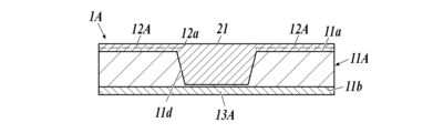
まず、本実施形態に係る印刷配線板の構成について説明する。図1は、本実施形態に係る印刷配線板100の断面図である。[Configuration of printed wiring board]
First, the configuration of the printed wiring board according to this embodiment will be explained. FIG. 1 is a cross-sectional view of a printed
本実施形態に係る印刷配線板100は、図1に示すように、第一基板1と、ビア2と、第二基板3と、絶縁層4と、で構成されている。
The printed
第一基板1(基板)は、本実施形態においては、印刷配線板100における最も端に積層されている。
この第一基板1は、第一絶縁層11と、第一配線12と、第二配線13と、を備えている。In this embodiment, the first substrate 1 (substrate) is laminated at the end of the printed
This
本実施形態に係る第一絶縁層11は、後述する第二基板3の第二絶縁層31を構成する材料とは異なる材料(例えばガラス繊維及びポリテトラフルオロエチレン:以下PTFE)で平板状に形成されている。
なお、第一絶縁層11を構成する材料には、PTFE以外の他のフッ素樹脂を用いることもできるし、フッ素樹脂以外の樹脂を用いることも可能である。
以下、第一絶縁層11の厚さ方向一端にある面(図1における下側の面)を第一面11aと称する。また、第一絶縁層11における第一面11aの裏面となる面(図1における上側の面)を第二面11bと称する。The first insulating
Note that for the material constituting the first insulating
Hereinafter, the surface at one end in the thickness direction of the first insulating layer 11 (the lower surface in FIG. 1) will be referred to as a
また、第一絶縁層11は、ビア下穴11cを有している。
ビア下穴11c(孔)は、第一絶縁層11を、当該第一絶縁層11の厚さ方向に貫通している。
第一面11a又は第二面11bと直交する方向から見たビア下穴11cは円形である。
また、本実施形態におけるビア下穴11cは、第一面11a側の径daと第二面11b側の径dbとが等しい。
また、本実施形態におけるビア下穴11cの内面は、第一面11a又は第二面11bと直交している。
なお、ビア下穴11cは、第一面11a側の径daが第二面11b側の径dbより小さくてもよいし、第一面11a側の径daが第二面11b側の径dbよりも大きくてもよい。このような場合(他の実施形態)については後述する。Further, the first insulating
The via
The via
Further, in the via
Moreover, the inner surface of the via
Note that the diameter d a on the
第一配線12は、第一絶縁層11の第一面11aに導電性材料(例えば銅)で形成されている。
第二配線13は、第一絶縁層11の第二面11bに導電性材料(例えば銅)で形成されている。
本実施形態に係る第一配線12及び第二配線13のうちの少なくともいずれかの配線は、電波を送受信するためのアンテナとして機能する形状である。The
The
At least one of the
ビア2は、導電性材料(例えば銅)でビア下穴11cの中を充填するフィルドビアである。
そして、ビア2は、第一基板1の第一,第二配線12,13と後述する第二基板3とを導通させている。
このビア2は、第一充填部21と、第二充填部22と、を有している。
また、本実施形態に係るビア2は、第一ランド部23と、第二ランド部24と、を有している。The via 2 is a filled via that fills the via
The
This via 2 has a first filling
Further, the via 2 according to the present embodiment includes a
第一充填部21は、少なくともビア下穴11cの中の中心部を、導電性材料(例えば銅)で充填している。
本実施形態に係る第一充填部21は、ビア下穴11cの中を充填するだけでなく、その一部が第一面11aよりもビア下穴11cの外側へ出ている。The
The
第二充填部22は、ビア下穴11cの中の第一充填部21によって充填されていない領域を、導電性材料(例えば銅)で充填している。
本実施形態に係る第二充填部22は、ビア下穴11cの中を充填するだけでなく、その一部が第二面11bよりもビア下穴11cの外側へ出ている。The
The
第一ランド部23は、導電性材料(例えば銅)で、第一面11aにおけるビア下穴11cの周囲に、第一充填部21と一体である。
また、第一ランド部23は、第一基板1の第一配線12と導通している。
第二ランド部24は、導電性材料(例えば銅)で、第二面11bにおけるビア下穴11cの周囲に、第二充填部22と一体である。
また、第二ランド部24は、第一基板1の第二配線13と導通している。The
Further, the
The
Further, the
第一充填部21と第二充填部22とはビア下穴11cの中で一体化している。しかし、第二充填部22と第一充填部21との間には、図1に一点鎖線で示したような界面Iが存在している。
この界面Iは、錐体面Iaと、上底面Ibを有している。
錐体面Iaは、第一面11aから第二面11bへ向かうに従って細くなるよう、第一面11aに対して所定角度θa傾斜している。
上底面Ibは、第二面11bと平行かつ第二面11bよりも第一面11a側へ所定距離d離れている。
界面Iは、このような錐体面Iaと、上底面Ibと、を有した円錐台状である。
第二面11bと上底面Ibとの距離dは、第一絶縁層11の厚さの半分を超えない長さである。The first filling
This interface I has a pyramidal surface I a and an upper base surface I b .
The pyramidal surface Ia is inclined at a predetermined angle θa with respect to the
The upper base surface Ib is parallel to the
The interface I has a truncated conical shape having such a conical surface I a and an upper base surface I b .
The distance d between the
第二基板3は、絶縁層4を介して、上記第一基板1の第一面11aに積層されている。
この第二基板3は、第二絶縁層31と、第三配線32と、を備えている。
第二絶縁層31及び絶縁層4は、絶縁材料(例えばガラス織布及びエポキシ樹脂)で平板状である。
第三配線32は、第二絶縁層31の表面に導電性材料(例えば銅)で形成されている。
なお、図1には、第二基板3として、1層の第二絶縁層31の両面に第三配線32がそれぞれ積層された2層基板を例示した。さらに、第二基板3は、複数の第二絶縁層31と第三配線32とが交互に積層された多層基板であってもよい。The
This
The second insulating
The
Note that FIG. 1 illustrates, as the
〔印刷配線板の製造方法〕
次に、上記印刷配線板100の製造方法について説明する。図2A、図2B、図2C、図2Dは印刷配線板100を製造する際の前半の工程を表す断面図である。図3A、図3B、図3C、図3D、図3E,図3Fは印刷配線板100を製造する際の後半の工程を表す断面図である。[Manufacturing method of printed wiring board]
Next, a method for manufacturing the printed
本実施形態に係る印刷配線板100の製造方法は、穴形成工程と、第一充填工程と、基板積層工程と、開口形成工程と、底壁除去工程と、第二充填工程と、回路形成工程と、を有する。
The method for manufacturing the printed
穴形成工程に先立ち、銅張積層板1Aを用意する。この銅張積層板1Aは、後に第一基板1となる部材である。
銅張積層板1Aとしては、例えば図2Aに示すように、絶縁層11Aと、絶縁層11Aの厚さ方向一端にある第一面11a全体に形成された第一銅箔層12Aと、絶縁層11Aにおける第一面11aの裏面となる第二面11b全体に形成された第二銅箔層13Aと、を備えたものを用いる。Prior to the hole forming step, a copper clad
As shown in FIG. 2A, for example, the copper-clad
初めの穴形成工程では、図2Bに示すように、絶縁層11Aの第一面11aに、有底のビア下穴11dを形成する。
ビア下穴11dの形成は、例えばレーザ加工により行う。
ビア下穴11dの形成には、様々な方法を用いることができる。
その一つとして、例えば、第一銅箔層12Aにおけるビア2を形成しようとする箇所に、サブトラクティブ法のエッチング等で第一開口12aを形成し、絶縁層11Aにおける第一開口12aから露出する部位にレーザ加工を行う方法がある。また、第一銅箔層12Aにおけるビア2を形成しようとする箇所に、事前に第一開口12aを形成することなく直接レーザ加工を行う方法もある。
また、レーザ加工を行う際、ビア下穴11dの形状が、のちに形成される第一充填部21の形状となるように、レーザの照射を調節する。
具体的には、ビア下孔1dの形状が、第一面11aにおける第一開口12aの縁から第二面11bへ向かうに従って細くなるよう所定角度θa傾斜する錐体面11eと、第二面11bと平行かつ第二面11bよりも第一面11a側へ所定距離d離れて位置する上底面11fと、を有する円錐台状となるようにする。In the first hole forming step, as shown in FIG. 2B, a bottomed via
The via
Various methods can be used to form the via
As one of the methods, for example, a
Further, when laser processing is performed, the laser irradiation is adjusted so that the shape of the via
Specifically, the shape of the via pilot hole 1d has a
以下、銅張積層板1Aにおけるビア下穴11dの上底面11fを形成する部位を底壁1aと称する。
この段階における底壁1aは、第二銅箔層13Aと、第二銅箔層13Aの表面に残留したスミアSと、が含まれる。
形成するビア下穴11dの深さによっては、底壁1aに、レーザで削られずに薄く残った絶縁層11AがスミアSとなる。
すなわち、穴形成工程では、形成したビア下穴11dの内面にスミアSを残してもよい。Hereinafter, a portion of the copper-clad
The bottom wall 1a at this stage includes the second
Depending on the depth of the via
That is, in the hole forming step, a smear S may be left on the inner surface of the formed via
なお、ビア下穴11dの内面にデスミア処理を施してもよい。ここで行うデスミア処理には、例えばO2プラズマ処理する等、ドライ方式を用いる。
また、ビア下穴11dの内面にソフトエッチングを施して、デスミア処理で除去し切れなかったスミアSを洗い流してもよい。
ただし、形成したビア下穴11dの形状によっては、ソフトエッチングの効果が十分に得られず、この段階ではスミアSが除去し切れない場合がある。Note that a desmear process may be performed on the inner surface of the via
Alternatively, soft etching may be performed on the inner surface of the via
However, depending on the shape of the formed via
ビア下穴11dを形成した後は、第一充填工程に移る。この工程では、電解フィルドめっきにより、図2Cに示すように、ビア下穴11d及び第一開口12aの中の空間を導電性材料(例えば銅)で充填する。
このビア下穴11d及び第一開口12aに充填された導電性材料は、ビア2の第一充填部21となる。After forming the via
The conductive material filled in the via
また、第一配線12を形成する。
第一配線12の形成は、ビア下穴11dを充填した後にサブトラクティブ法を用いて行ってもよいし、MSAP(Modified Semi Additive Process)を用いてビア下穴11dの充填と並行して行ってもよい。
第一配線12が形成されると、図2Dに示したように、第一銅箔層12Aからビア2の第一ランド部23が形成される。In addition, the
The
When the
ビア下穴11dを充填した後は、基板積層工程に移る。この工程では、図3A,図3Bに示すように、第一面11a側が加工された銅張積層板1Aの第一面11aに、第二基板3を、半硬化状態の絶縁材料であるプリプレグ4pを介して積層する。
積層後、銅張積層板1Aの絶縁層11Aは、第一絶縁層11となる。
また、プリプレグ4pは、硬化後、第二基板3に隣接する第一基板1側の絶縁層4となる。After filling the via
After lamination, the insulating
Further, after curing, the
銅張積層板1Aに第二基板3を積層した後は、開口形成工程に移る。この工程では、銅張積層板1Aの第二銅箔層13Aにおけるビア2を形成しようとする箇所に、図3Cに示すように第二開口13aを形成する。本実施形態においては、この第二開口13aの径(後に形成されるビア下穴11cの第二面11b側の径dbと等しい)が、上記穴形成工程で形成したビア下穴11dの第一面11aにおける径daと等しくする。
第二開口13aの形成は、例えばサブトラクティブ法でエッチングする。After laminating the
The
第二開口13aを形成した後は、底壁除去工程に移る。この工程では、銅張積層板1Aの第二面11b側において、ビア下穴11dの少なくとも底壁1aを除去する。
本実施形態においては、第二開口13aの径dbが、ビア下穴11dの上底面11fの径dfよりも大きい。このため、ビア下穴11dの底壁1aに加え、第一絶縁層11におけるビア下穴11dの錐体面11eを形成する部位である側壁11hも、第二開口13aの縁を通り第二面11bと直交する面で切り取られて除去される。
底壁1a及び側壁11hの除去は、例えばレーザ加工により行う。
底壁1a及び側壁11hが除去されると、図3Dに示すように、第一充填部21の上底面21b、及び第一充填部21の錐体面21a全体が露出する。After forming the
In this embodiment, the diameter db of the
The bottom wall 1a and the
When the bottom wall 1a and the
また、底壁1a及び側壁11hが除去されると、ビア下穴11dが第一絶縁層11を貫通し、ビア下穴11cとなる。
そして、ビア下穴11cの内面にデスミア処理を施すことにより、底壁1a及び側壁11hを除去した後にビア下穴11c内面及び第一充填部21表面に残ったスミアSを除去する。
ここで行うデスミア処理にも、O2プラズマ処理する等、ドライ方式の方法を用いる。
また、ビア下穴11cの内面にソフトエッチングを施すことにより、デスミア処理で除去し切れなかったスミアSを洗い流す。
これにより、スミアSを含むビア下穴11dの底壁1aを形成していたものが完全に除去される。Further, when the bottom wall 1a and the
Then, by performing a desmear process on the inner surface of the via
The desmear treatment performed here also uses a dry method such as O 2 plasma treatment.
Furthermore, by performing soft etching on the inner surface of the via
As a result, the smear S that forms the bottom wall 1a of the via
ビア下穴11dの底壁1aを除去した後は、第二充填工程へ移る。この工程では、電解フィルドめっきにより、図3Eに示すように、ビア下穴11dの底壁1aが除去された後にできる空間を導電性材料(例えば銅)で充填するとともに、第二銅箔層13Aの表面にめっき層13Bを形成する。
この空間に充填された導電性材料は、ビア2の第二充填部22となる。
また、第二充填部22が形成されると、第二充填部22と第一充填部21とによって円錐台状の界面Iが形成される。After removing the bottom wall 1a of the via
The conductive material filled in this space becomes the second filling
Moreover, when the second filling
導電性材料を充填した後は、回路形成工程に移る。この工程では、第二充填部22の表面及びめっき層13Bにおける後に第二配線13となる部位の表面にエッチングレジストを形成し、エッチングを施す。
エッチングが施されると、図3Fに示すように、めっき層13B及び第二銅箔層13Aから不要な部分が除去され、ビア2の第二ランド部24、及び第二配線13が形成される。After filling the conductive material, the process moves to a circuit formation step. In this step, an etching resist is formed on the surface of the
When etching is performed, as shown in FIG. 3F, unnecessary parts are removed from the
以上説明してきたように、本実施形態に係る印刷配線板100は、絶縁層11Aに円錐台状のビア下穴11dを形成し、第一充填部21を形成し、ビア下穴11dの底壁1aを除去し、最後に残ったスミアSを完全に除去してから、第二充填部22を形成することにより得られる。
このため、第一絶縁層11に用いる材料と形成しようとするビア2のサイズ(径、深さ)のうちの少なくとも一方に制約があっても、スミアSの残留が無くかつ十分に充填されたビアを印刷配線板100に形成できる。
また、本実施形態の第一絶縁層11の材料であるPTFEは、加工性が悪い材料であるが、本実施形態の製造方法を用いれば、加工が容易である。
また、PTFEは、吸水性を有するが、デスミア処理を行う際にドライ方式を用いることで、PTFEで形成された絶縁層11Aの膨張を防ぐことができる。As described above, in the printed
Therefore, even if there are restrictions on at least one of the material used for the first insulating
Further, although PTFE, which is the material of the first insulating
Further, although PTFE has water absorbing properties, by using a dry method when desmearing, it is possible to prevent the
また、ビア下穴11dの径が大きい場合又は深い場合であっても、ビア下穴11dの充填は容易である。
また、ビア2が十分に充填されないという異常は低減できる。
また、ビア下穴11dの径が大きい場合又は深い場合であっても、ビア下穴11dの上底面11fに残留したスミアSは容易に除去できる。
また、応力が掛かりやすいビア2の第二充填部22の径(ビア下穴11cの第二面11b側の径dbと等しい)が、小さくなっていないため、ビア2の導通性能の信頼性を高めることができる。
また、ビア2の第二充填部22の径dbが、第一開口12aの径(ビア下穴11dの第一面11aにおける径daと等しい)と等しくなるため、第二充填部22の径dbを含むビア2の第二面11b側の径を容易にコントロールすることができる。Further, even if the diameter of the via
Furthermore, the abnormality that the via 2 is not sufficiently filled can be reduced.
Further, even if the diameter of the via
In addition, the diameter of the second filled
Furthermore, since the diameter db of the
(他の実施形態1)
なお、上記実施形態においては、印刷配線板100として、ビア下穴11cの第一面11a側の径daと第二面11b側の径dbが等しく、かつビア下穴11cの内面が第一面11a又は第二面11bと直交しているものを例示した。他の実施形態としてはビア下穴11cの第一面11a側の径daと第二面11b側の径dbを等しくするとともに、ビア下穴11cの内面を第一面11aに対して傾斜させてもよい。
このような印刷配線板100Aを製造する方法は、図4Aに示すように、開口形成工程(図3C参照)までは上記実施形態と同じとなる。(Other Embodiment 1)
In the above embodiment, the printed
As shown in FIG. 4A, the method for manufacturing such a printed
他の実施形態1においても上記実施形態と同様、第二開口13aの径dbが、ビア下穴11dの上底面11fの径dfよりも大きいため、次の底壁除去工程では、底壁1aに加え、側壁11hの一部を除去することになる。
しかし、ここでは、除去する部位の切断面が、図4Bに示すように、第二面11bにおける第二開口13aの縁から第一面11aへ向かうに従って細くなり、かつ第二面11bに対して所定角度θb傾斜する錐体面11iとなるように、レーザの照射を調節する。この角度θbは、第一面11a側からビア下穴11dを形成する際の錐体面11eの角度θaと同じでもよいし異なっていてもよい。In
However, here, as shown in FIG. 4B, the cut surface of the part to be removed becomes thinner as it goes from the edge of the
ビア下穴11dの底壁1a及び側壁11hの一部が除去されると、ビア下穴11dが第一絶縁層11を貫通し、ビア下穴11cが形成される。
その際、第一面11a側から形成したビア下穴11dの錐体面11eと、側壁11hの一部を除去することで形成される錐体面11iとが、第一絶縁層11の厚さ方向中間部で交差する。
すなわち、ビア下穴11cの形状は、第一絶縁層11の厚さ方向中間部で円錐台同士が上底面を向い合せた(中間部がくびれた)形状となる。When the bottom wall 1a and part of the
At that time, the
That is, the shape of the via
その後、図4Cに示す第二充填工程及び回路形成工程を経て、図4Dに示すように、上記実施形態とはビア下穴11cと第二充填部22の形状が異なる他の実施形態1の印刷配線板100Aが製造される。
上記実施形態の場合には、第二充填部22と第一充填部21とによって円錐台状の界面Iが形成された。一方、他の実施形態1の場合は、第二充填部22と第一充填部21とによって上記実施形態よりも低い円錐台状の界面Iが形成される。しかし、第一充填部21全体の輪郭は、上記第一実施形態の界面Iと類似の円錐台状となる。After that, through the second filling process and circuit forming process shown in FIG. 4C, as shown in FIG.
In the case of the embodiment described above, a truncated conical interface I was formed by the second filling
レーザ加工は、奥に向かうに従って径が狭まる(すり鉢状の)穴の加工に向いているため、他の実施形態1のようにすれば、上記実施形態で挙げた効果に加え、上記実施形態よりもビア下穴11cを容易に形成することができる、という効果が得られる。
Laser machining is suitable for machining holes whose diameter narrows toward the back (mortar-shaped), so if it is done as in
(他の実施形態2)
また、上記実施形態及び他の実施形態1と異なり、ビア下穴11cの第二面11b側の径dbを第一面11a側の径daより小さくしてもよい。
この場合には、第二面11b側の径dbをビア下穴11dの上底面11fの径dfより小さくする形成例1と、上底面11fの径dfと等しくする形成例2と、がある。(Other Embodiment 2)
Further, unlike the above embodiment and the
In this case, there is a formation example 1 in which the diameter db on the
・形成例1
ビア下穴11cの第二面11b側の径dbがビア下穴11dの上底面11fの径dfより小さい印刷配線板100Bを製造する方法は、基板積層工程(図3B参照)までは上記実施形態と同じとなる。
次の開口形成工程では、銅張積層板1Aの第二銅箔層13Aにおける、ビア2を形成しようとする箇所に、図5Aに示すように、ビア下穴11dの上底面11fの径dfより小さい径dbの第二開口13aを、上記実施形態と同一の方法で形成する。
なお、第二開口13aの径dbの大きさは、これから形成されるビアが所定の大きさの電流を流すことのできる太さを下回らないようにする。・Formation example 1
The method for manufacturing the printed
In the next opening forming step, in the second
Note that the diameter db of the
他の実施形態2においては、第二開口13aから、第一絶縁層11の底壁1aの一部(周縁部を除いた中央部)のみが露出するため、次の底壁除去工程では、底壁1aの一部のみを除去することになる。
底壁1aの一部が除去されると、図5Bに示すように、円錐台状のビア下穴11dの上底面11fに、上底面11fより一回り小さい円板を重ね合わせたような形状のビア下穴11cが形成される。In the second embodiment, only a part of the bottom wall 1a of the first insulating layer 11 (the central part excluding the periphery) is exposed from the
When a part of the bottom wall 1a is removed, as shown in FIG. 5B, a disk shaped like a disc one size smaller than the
その後、図5Cに示す第二充填工程及び回路形成工程を経て、図5Dに示すように、上記実施形態及び他の実施形態1とはビア下穴11cと第二充填部22の形状が異なる他の実施形態2の印刷配線板100Bが製造される。
他の実施形態2の場合は、第二充填部22と第一充填部21とによって平面状の界面Iが形成される。しかし、第二充填部22及び第一絶縁層11と、第一充填部21と、の間に存在する界面(第一充填部21全体の輪郭)は、上記第一実施形態の界面Iと類似の円錐台状となる。Thereafter, through a second filling step and a circuit forming step shown in FIG. 5C, as shown in FIG. A printed
In the case of the second embodiment, a planar interface I is formed by the second filling
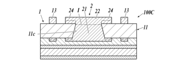
・形成例2
一方、ビア下穴11cの第二面11b側の径dbがビア下穴11dの上底面11fの径dfと等しい印刷配線板100Cを製造する方法も、基板積層工程(図3B参照)までは上記実施形態と同じである。
次の開口形成工程では、銅張積層板1Aの第二銅箔層13Aにおける、ビア2を形成しようとする箇所に、図6Aに示すように、ビア下穴11dの上底面11fの径dfと等しい径dbの第二開口13aを、上記実施形態と同一の方法で形成する。・Formation example 2
On the other hand, the method of manufacturing the printed
In the next opening forming step, in the second
他の実施形態2においては、第二開口13aから、第一絶縁層11の底壁1a全体のみが露出するため、次の底壁除去工程では、底壁1a全体のみを除去する。
In the second embodiment, only the entire bottom wall 1a of the first insulating
底壁1a全体が除去されると、図6Bに示すように、円錐台状のビア下穴11dの上底面11fに、上底面11fと同径の円板を重ね合わせたような形状のビア下穴11cが形成される。
When the entire bottom wall 1a is removed, as shown in FIG. 6B, a via bottom shaped like a disk having the same diameter as the
その後、図6Cに示す第二充填工程及び回路形成工程を経て、図6Dに示すように、上記実施形態及び他の実施形態1,2とはビア下穴11cと第二充填部22の形状が異なる他の実施形態2の印刷配線板100Cが製造される。
他の実施形態2の場合は、上記形成例2と同様に、第二充填部22と第一充填部21とによって平面状の界面Iが形成される。しかし、第二充填部22及び第一絶縁層11と、第一充填部21と、の間に存在する界面(第一充填部21全体の輪郭)は、上記第一実施形態の界面Iと類似の円錐台状となる。Thereafter, through the second filling step and circuit forming step shown in FIG. 6C, as shown in FIG. 6D, the shape of the via
In the case of the
他の実施形態2のいずれかの形成例のようにすれば、ビア2の第二充填部22の径dbが小さくなるため、第二ランド部24の径を小さくすることができる。このため、他の実施形態2のようにすれば、上記実施形態で挙げた効果に加え、第二配線13の形成に使用できるスペースが広がり、第二配線13の設計の自由度を高める効果が得られる。If the formation example of any of the
(他の実施形態3)
また、上記実施形態及び他の実施形態1,2と異なり、ビア下穴11cの第二面11b側の径dbを第一面11a側の径daより大きくしてもよい。
このような印刷配線板100Dを製造する方法は、基板積層工程(図3B参照)までは上記実施形態と同じである。
次の開口形成工程では、銅張積層板1Aの第二銅箔層13Aにおける、ビア2を形成しようとする箇所に、図7Aに示すように、ビア下穴11dの上底面11fの径dfより大きい径dbの第二開口13aを、上記実施形態と同一の方法で形成する。(Other Embodiment 3)
Further, unlike the above embodiment and
The method for manufacturing such a printed
In the next opening forming step, in the second
他の実施形態3においては、第二開口13aの径dbが、ビア下穴11dの第一面11a側の径daよりも大きいため、次の底壁除去工程では、底壁1aに加え、側壁11hも除去する。
ここでは、除去する部位の切断面が、第二面11bにおける第二開口13aの縁から第一面11aへ向かうに従って細くなるよう所定角度θb傾斜する錐体面11iとなるように、レーザの照射を調節する。In
Here, the laser irradiation is performed so that the cut surface of the part to be removed becomes a conical surface 11i that is inclined at a predetermined angle θ b so that it becomes narrower from the edge of the
ビア下穴11dの底壁1a及び側壁11hが除去されると、図7Bに示すように、第二面11bから第一面11aへ向かうに従って細くなり、かつ第二面11bに対して所定角度θb傾斜する錐体面11iを有する円錐台状のビア下穴11cとなる。When the bottom wall 1a and
その後、図7Cに示す第二充填工程及び回路形成工程を経て、図7Dに示すように、上記実施形態及び変形例1,2とはビア下穴11cと第二充填部22の形状が異なる他の実施形態3の印刷配線板100Dが製造される。
他の実施形態3の場合は、上記実施形態と同様に、第二充填部22と第一充填部21とによって円錐台状の界面Iが形成される。Thereafter, through the second filling step and circuit forming step shown in FIG. 7C, as shown in FIG. 7D, the shape of the via
In the case of the third embodiment, a truncated conical interface I is formed by the second filling
他の実施形態3のようにすれば、上記実施形態で挙げた効果に加え、大口径のビア2を形成でき、ビア2の導通性能の信頼性をより一層高める効果が得られる。
If the
本開示の内容は、印刷配線板及び印刷配線板の製造方法に利用することができる。 The content of the present disclosure can be used in printed wiring boards and methods for manufacturing printed wiring boards.
100,100A,100B,100C,100D 印刷配線板
1 第一基板(基板)
11 第一絶縁層(絶縁層)
11a 第一面
11b 第二面
11c ビア下穴(孔)
12 第一配線
13 第二配線
1A 銅張積層板
1a 底壁
11A 絶縁層
11d ビア下穴
11e 錐体面
11f 上底面
11h 側壁
11i 錐体面
12A 第一銅箔層
12a 第一開口
13A 第二銅箔層
13a 第二開口
13B めっき層
2 ビア
21 第一充填部
21a 錐体面
21b 上底面
22 第二充填部
23 第一ランド部
24 第二ランド部
3 第二基板
31 第二絶縁層
32 第三配線
4 絶縁層
4p プリプレグ
d 第二面と錐体面との距離
da ビア下穴の第一面側(開口)の径
db ビア下穴の第二面側(開口)の径
df ビア下穴(第一充填部)の上底面の径
I 界面
Ia 錐体面
Ib 上底面
S スミア
θa 第一面と錐体面とがなす角度
θb 第二面と錐体面とがなす角度100, 100A, 100B, 100C, 100D Printed wiring
11 First insulation layer (insulation layer)
12
Claims (10)
前記ビアは、少なくとも前記孔の中の中心部を前記電解めっき銅で充填する第一充填部と、前記孔の中の前記第一充填部によって充填されていない領域を前記電解めっき銅で充填する第二充填部と、を有し、
前記第二充填部と前記第一充填部との間に存在する界面、又は前記第二充填部及び前記第一絶縁層と前記第一充填部との間に存在する界面は、前記第一絶縁層の厚さ方向一端にある第一面から前記第一絶縁層における前記第一面の裏面となる第二面へ向かうに従って細くなるよう傾斜する錐体面と、前記第二面と平行かつ前記第二面よりも前記第一面側へ位置する上底面と、を有する円錐台状になっており、前記第一充填部は、その一部が前記第一面よりも前記孔の外側へ出て、前記第一面において前記孔の周囲に位置する第一ランド部と一体であり、前記第二充填部は、その一部が前記第二面よりも前記孔の外側へ出て、前記第二面において前記孔の周囲に位置する第二ランド部と一体である印刷配線板。 A printed wiring board comprising: a first substrate having a first insulating layer having a flat plate shape and having a hole penetrating through the thickness; and a via filling the hole with electroplated copper ,
The via includes a first filling portion that fills at least a central portion of the hole with the electrolytically plated copper , and a region of the hole that is not filled by the first filling portion that is filled with the electrolytically plated copper. a second filling part;
The interface existing between the second filling part and the first filling part, or the interface existing between the second filling part and the first insulating layer and the first filling part, a conical surface that is inclined to become narrower as it goes from a first surface at one end in the thickness direction of the layer to a second surface that is the back surface of the first surface in the first insulating layer; The first filling portion has a truncated conical shape, and has an upper bottom surface located closer to the first surface than the second surface, and a portion of the first filling portion protrudes to the outside of the hole relative to the first surface. , the second filling portion is integral with a first land portion located around the hole on the first surface, and a portion of the second filling portion protrudes outside the hole beyond the second surface, and the second filling portion is integral with the first land portion located around the hole; A printed wiring board that is integral with a second land portion located around the hole in a plane thereof .
前記絶縁層の厚さ方向一端にある第一面において、前記第一面から前記絶縁層における前記第一面の裏面となる第二面へ向かうに従って細くなるよう傾斜する錐体面と、前記第二面と平行かつ前記第二面よりも前記第一面側へ位置する上底面と、を有する円錐台状の有底の穴を形成する穴形成工程と、
前記穴を導電性材料で充填し第一充填部を形成する第一充填工程と、
前記第二面側において、少なくとも前記穴の底壁を除去して前記導電性材料を露出させる底壁除去工程と、
前記底壁が除去された後にできる空間に導電性材料を充填することによりビアを形成する第二充填工程と、を有する印刷配線板の製造方法。 A method for manufacturing a printed wiring board using a copper-clad laminate having an insulating layer formed in a flat plate shape, the method comprising:
a first surface at one end in the thickness direction of the insulating layer; a pyramidal surface that is inclined to become narrower as it goes from the first surface to a second surface of the insulating layer that is the back surface of the first surface; a hole forming step of forming a truncated conical bottomed hole having an upper bottom surface parallel to the surface and located closer to the first surface than the second surface;
a first filling step of filling the hole with a conductive material to form a first filling part;
a bottom wall removing step of removing at least the bottom wall of the hole to expose the conductive material on the second surface side;
A method for manufacturing a printed wiring board, comprising: a second filling step of forming a via by filling a conductive material into a space created after the bottom wall is removed.
前記底壁除去工程において、レーザ加工により少なくとも前記底壁を除去し、さらにデスミア処理及びソフトエッチングを施すことにより、前記底壁を除去した後に残ったスミアを除去する請求項8に記載の印刷配線板の製造方法。 In the hole forming step, a smear is left on the inner surface of the formed hole,
9. The printed wiring according to claim 8 , wherein in the bottom wall removal step, at least the bottom wall is removed by laser processing, and the smear remaining after the bottom wall is removed is further removed by desmear treatment and soft etching. Method of manufacturing the board.
Applications Claiming Priority (3)
| Application Number | Priority Date | Filing Date | Title |
|---|---|---|---|
| JP2018143120 | 2018-07-31 | ||
| JP2018143120 | 2018-07-31 | ||
| PCT/JP2019/029584 WO2020027022A1 (en) | 2018-07-31 | 2019-07-29 | Printed-wiring board and method of manufacturing printed-wiring board |
Publications (2)
| Publication Number | Publication Date |
|---|---|
| JPWO2020027022A1 JPWO2020027022A1 (en) | 2021-08-02 |
| JP7366025B2 true JP7366025B2 (en) | 2023-10-20 |
Family
ID=69231772
Family Applications (1)
| Application Number | Title | Priority Date | Filing Date |
|---|---|---|---|
| JP2020533519A Active JP7366025B2 (en) | 2018-07-31 | 2019-07-29 | Printed wiring board and method for manufacturing printed wiring board |
Country Status (5)
| Country | Link |
|---|---|
| US (1) | US11540390B2 (en) |
| EP (1) | EP3833165A4 (en) |
| JP (1) | JP7366025B2 (en) |
| CN (1) | CN112514544B (en) |
| WO (1) | WO2020027022A1 (en) |
Families Citing this family (1)
| Publication number | Priority date | Publication date | Assignee | Title |
|---|---|---|---|---|
| JP2021132068A (en) * | 2020-02-18 | 2021-09-09 | イビデン株式会社 | Printed wiring board and manufacturing method of the same |
Citations (7)
| Publication number | Priority date | Publication date | Assignee | Title |
|---|---|---|---|---|
| JP2008235624A (en) | 2007-03-22 | 2008-10-02 | Kyocer Slc Technologies Corp | Wiring circuit board and manufacturing method therefor |
| JP2014154631A (en) | 2013-02-06 | 2014-08-25 | Toppan Printing Co Ltd | Multilayer wiring board and manufacturing method of the same |
| JP2015198128A (en) | 2014-03-31 | 2015-11-09 | 京セラサーキットソリューションズ株式会社 | Printed-circuit board and method for manufacturing the same |
| WO2016114400A1 (en) | 2015-01-15 | 2016-07-21 | コニカミノルタ株式会社 | Laminated wiring structure, and methdod for forming laminated wiring structure |
| JP2017107934A (en) | 2015-12-08 | 2017-06-15 | 富士通株式会社 | Circuit board, electronic apparatus, and method of manufacturing circuit board |
| JP2019160885A (en) | 2018-03-08 | 2019-09-19 | スタンレー電気株式会社 | Circuit board, electronic circuit device, and manufacturing method of circuit board |
| JP2019201140A (en) | 2018-05-17 | 2019-11-21 | スタンレー電気株式会社 | Multilayer circuit board and method for manufacturing the same |
Family Cites Families (18)
| Publication number | Priority date | Publication date | Assignee | Title |
|---|---|---|---|---|
| JP2920854B2 (en) * | 1991-08-01 | 1999-07-19 | 富士通株式会社 | Via hole structure and method of forming the same |
| TW506242B (en) * | 1999-12-14 | 2002-10-11 | Matsushita Electric Ind Co Ltd | Multi-layered printed circuit board and method for manufacturing the same |
| JP4054269B2 (en) * | 2003-03-20 | 2008-02-27 | Tdk株式会社 | Electronic component manufacturing method and electronic component |
| US7834273B2 (en) * | 2005-07-07 | 2010-11-16 | Ibiden Co., Ltd. | Multilayer printed wiring board |
| JP5021216B2 (en) * | 2006-02-22 | 2012-09-05 | イビデン株式会社 | Printed wiring board and manufacturing method thereof |
| US20080053688A1 (en) * | 2006-09-01 | 2008-03-06 | Samsung Electro-Mechanics Co., Ltd. | Printed circuit board and method of manufacturing the same |
| KR101542478B1 (en) * | 2007-08-15 | 2015-08-06 | 테세라, 인코포레이티드 | A method of fabricating an interconnection element having conductive posts |
| US8272126B2 (en) * | 2008-04-30 | 2012-09-25 | Panasonic Corporation | Method of producing circuit board |
| US8563873B2 (en) * | 2009-03-31 | 2013-10-22 | Ibiden Co., Ltd. | Substrate with metal film and method for manufacturing the same |
| JP5419583B2 (en) | 2009-08-03 | 2014-02-19 | 新光電気工業株式会社 | Wiring board manufacturing method |
| TWI399150B (en) * | 2009-12-31 | 2013-06-11 | Unimicron Technology Corp | Circuit board and process for fabricating the same |
| JP2013073970A (en) * | 2011-09-26 | 2013-04-22 | Dainippon Printing Co Ltd | Multilayer wiring board and manufacturing method therefor |
| JP5865771B2 (en) * | 2012-04-26 | 2016-02-17 | 日本特殊陶業株式会社 | Multilayer wiring board |
| US20140166355A1 (en) * | 2012-12-18 | 2014-06-19 | Samsung Electro-Mechanics Co., Ltd. | Method of manufacturing printed circuit board |
| JP6639775B2 (en) * | 2014-10-21 | 2020-02-05 | 住友電工プリントサーキット株式会社 | Resin film, coverlay for printed wiring board, printed wiring board substrate and printed wiring board |
| FR3041482B1 (en) * | 2015-09-21 | 2017-12-15 | Commissariat Energie Atomique | DETERMINING A SPATIAL DISTRIBUTION OF A THERMAL EVACUATION PARAMETER OF AN ELECTROCHEMICAL CELL |
| CN209964380U (en) * | 2018-10-26 | 2020-01-17 | 奥特斯(中国)有限公司 | Part carrier with laser via hole |
| US10950463B2 (en) * | 2019-01-31 | 2021-03-16 | At&S Austria Technologie & Systemtechnik Aktiengesellschaft | Manufacturing trapezoidal through-hole in component carrier material |
-
2019
- 2019-07-29 CN CN201980050181.XA patent/CN112514544B/en active Active
- 2019-07-29 US US17/263,187 patent/US11540390B2/en active Active
- 2019-07-29 JP JP2020533519A patent/JP7366025B2/en active Active
- 2019-07-29 WO PCT/JP2019/029584 patent/WO2020027022A1/en unknown
- 2019-07-29 EP EP19845297.1A patent/EP3833165A4/en not_active Withdrawn
Patent Citations (7)
| Publication number | Priority date | Publication date | Assignee | Title |
|---|---|---|---|---|
| JP2008235624A (en) | 2007-03-22 | 2008-10-02 | Kyocer Slc Technologies Corp | Wiring circuit board and manufacturing method therefor |
| JP2014154631A (en) | 2013-02-06 | 2014-08-25 | Toppan Printing Co Ltd | Multilayer wiring board and manufacturing method of the same |
| JP2015198128A (en) | 2014-03-31 | 2015-11-09 | 京セラサーキットソリューションズ株式会社 | Printed-circuit board and method for manufacturing the same |
| WO2016114400A1 (en) | 2015-01-15 | 2016-07-21 | コニカミノルタ株式会社 | Laminated wiring structure, and methdod for forming laminated wiring structure |
| JP2017107934A (en) | 2015-12-08 | 2017-06-15 | 富士通株式会社 | Circuit board, electronic apparatus, and method of manufacturing circuit board |
| JP2019160885A (en) | 2018-03-08 | 2019-09-19 | スタンレー電気株式会社 | Circuit board, electronic circuit device, and manufacturing method of circuit board |
| JP2019201140A (en) | 2018-05-17 | 2019-11-21 | スタンレー電気株式会社 | Multilayer circuit board and method for manufacturing the same |
Also Published As
| Publication number | Publication date |
|---|---|
| US20210185812A1 (en) | 2021-06-17 |
| CN112514544A (en) | 2021-03-16 |
| JPWO2020027022A1 (en) | 2021-08-02 |
| CN112514544B (en) | 2024-04-19 |
| EP3833165A4 (en) | 2022-05-04 |
| US11540390B2 (en) | 2022-12-27 |
| WO2020027022A1 (en) | 2020-02-06 |
| EP3833165A1 (en) | 2021-06-09 |
Similar Documents
| Publication | Publication Date | Title |
|---|---|---|
| US6548767B1 (en) | Multi-layer printed circuit board having via holes formed from both sides thereof | |
| JP2006041463A (en) | Conductive column manufacturing method and circuit board having conductive column | |
| JP6870608B2 (en) | Printed wiring board and its manufacturing method | |
| KR101506785B1 (en) | Printed Circuit Board | |
| JP2007227929A (en) | Printed circuit board having inner via hole and manufacturing method thereof | |
| CN103874326A (en) | Printed circuit board and method of manufacturing printed circuit board | |
| WO2016063799A1 (en) | Flexible printed wiring board and method for manufacturing same | |
| JP4256603B2 (en) | Manufacturing method of laminated wiring board | |
| JP7366025B2 (en) | Printed wiring board and method for manufacturing printed wiring board | |
| US7393720B2 (en) | Method for fabricating electrical interconnect structure | |
| CN110505758B (en) | Circuit board structure and manufacturing method thereof | |
| JP2017084914A (en) | Printed wiring board and method of manufacturing the same | |
| JP2009060151A (en) | Production process of laminated wiring board | |
| JP2006210748A (en) | Structure and processing method of built-up printed-wiring board | |
| JP7397718B2 (en) | Printed wiring board and method for manufacturing printed wiring board | |
| WO2021200538A1 (en) | Printed wiring board and method for manufacturing printed wiring board | |
| JP4963495B2 (en) | Laminated wiring board and manufacturing method thereof | |
| JP2019029559A (en) | Multilayer wiring board and manufacturing method thereof | |
| US20220338348A1 (en) | Circuit board and method for manufacturing the same | |
| JP5157583B2 (en) | Manufacturing method of build-up multilayer wiring board | |
| KR20160014432A (en) | Insulating film, printed circuit board using the same and method for manufacturing thereof | |
| CN119342690A (en) | Circuit board and method for manufacturing the same | |
| JP2013062292A (en) | Multilayer wiring board and manufacturing method of the same | |
| JP2006253372A (en) | Multi-layer printed wiring board and its manufacturing method | |
| JP2005286122A (en) | Printed wiring board and its manufacturing method |
Legal Events
| Date | Code | Title | Description |
|---|---|---|---|
| A621 | Written request for application examination |
Free format text: JAPANESE INTERMEDIATE CODE: A621 Effective date: 20220601 |
|
| A131 | Notification of reasons for refusal |
Free format text: JAPANESE INTERMEDIATE CODE: A131 Effective date: 20230404 |
|
| A521 | Request for written amendment filed |
Free format text: JAPANESE INTERMEDIATE CODE: A523 Effective date: 20230531 |
|
| TRDD | Decision of grant or rejection written | ||
| A01 | Written decision to grant a patent or to grant a registration (utility model) |
Free format text: JAPANESE INTERMEDIATE CODE: A01 Effective date: 20230919 |
|
| A61 | First payment of annual fees (during grant procedure) |
Free format text: JAPANESE INTERMEDIATE CODE: A61 Effective date: 20231010 |
|
| R150 | Certificate of patent or registration of utility model |
Ref document number: 7366025 Country of ref document: JP Free format text: JAPANESE INTERMEDIATE CODE: R150 |