JP5419583B2 - Wiring board manufacturing method - Google Patents
Wiring board manufacturing method Download PDFInfo
- Publication number
- JP5419583B2 JP5419583B2 JP2009180388A JP2009180388A JP5419583B2 JP 5419583 B2 JP5419583 B2 JP 5419583B2 JP 2009180388 A JP2009180388 A JP 2009180388A JP 2009180388 A JP2009180388 A JP 2009180388A JP 5419583 B2 JP5419583 B2 JP 5419583B2
- Authority
- JP
- Japan
- Prior art keywords
- layer
- wiring
- via hole
- resin
- wiring layer
- Prior art date
- Legal status (The legal status is an assumption and is not a legal conclusion. Google has not performed a legal analysis and makes no representation as to the accuracy of the status listed.)
- Active
Links
Images


Description
本発明は配線基板の製造方法に係り、さらに詳しくは、ビルドアップ工法で配線層を形成する方法に適用できる配線基板の製造方法に関する。 The present invention relates to a method for manufacturing a wiring board, and more particularly to a method for manufacturing a wiring board that can be applied to a method for forming a wiring layer by a build-up method.
従来、ビルドアップ工法によって形成される多層配線を有する配線基板がある。ビルドアップ工法では、絶縁層の形成、ビアホールの形成、電解めっきを使用する配線形成などを繰り返すことによって多層配線を形成することができる。 Conventionally, there is a wiring board having a multilayer wiring formed by a build-up method. In the build-up method, multilayer wiring can be formed by repeating formation of an insulating layer, formation of a via hole, wiring formation using electrolytic plating, and the like.
特許文献1には、半導体装置用多層基板において、半導体素子搭載層側から外部接続端子の方向に配線を順次積層することにより、半導体素子搭載層を平坦面とすることが記載されている。
特許文献2には、多層プリント配線板の製造方法において、ビアホールの底部の導体層をエッチングし、ビアホールの周壁を除去した後に、ビアホール内にめっき層を形成する方法が記載されている。
後述する関連技術の欄で説明するように、セミアディティブ法を使用して多層配線を形成する際には、配線層上の樹脂層にレーザでビアホールを形成した後に、ビアホール内の樹脂スミアを除去するためにデスミア処理を行う必要がある。 As explained in the related technology section below, when forming a multilayer wiring using the semi-additive method, after forming a via hole in the resin layer on the wiring layer with a laser, the resin smear in the via hole is removed. In order to do so, it is necessary to perform desmear processing.
このとき、デスミア処理によってビアホールの下部の樹脂層が外側にエッチングされる傾向があり、ビアホールの下部にえぐれ部が形成されてしまう。近年では、配線層の微細化の要求から、スパッタ法でシード層を薄膜で形成することが求められている。 At this time, the resin layer under the via hole tends to be etched outward by the desmear process, and a hollow portion is formed under the via hole. In recent years, due to the demand for miniaturization of the wiring layer, it is required to form the seed layer as a thin film by sputtering.
無電解めっきでシード層を形成する場合は、ビアホールのえぐれ部にもシード層を形成できるが、スパッタ法でシード層を形成する場合は、ビアホールのえぐれ部にシード層を形成することは困難である。 When the seed layer is formed by electroless plating, the seed layer can also be formed in the via hole, but when the seed layer is formed by sputtering, it is difficult to form the seed layer in the via hole. is there.
従って、ビアホールのえぐれ部にシード層が存在しない状態で、電解めっきに基づいて配線層を形成すると、ビアホールの底部のえぐれ部がボイド(空間)となってしまい、配線基板の信頼性が得られない問題がある。 Therefore, if a wiring layer is formed based on electrolytic plating in the absence of a seed layer in the via hole, the bottom of the via hole becomes a void (space), and the reliability of the wiring board is obtained. There is no problem.
本発明は以上の課題を鑑みて創作されたものであり、ビアホール内にスパッタ法でシード層を形成し、その上に電解金属めっき層を形成することに基づいて配線層を形成する配線基板の製造方法において、信頼性よく配線層を形成できる方法を提供することを目的とする。 The present invention has been created in view of the above problems, and is a wiring board for forming a wiring layer based on forming a seed layer in a via hole by a sputtering method and forming an electrolytic metal plating layer thereon. An object of the present invention is to provide a method for forming a wiring layer with high reliability in a manufacturing method.
上記課題を解決するため、本発明は、配線基板の製造方法に係り、仮基板の上に分離できる状態で樹脂層を形成する工程と、前記樹脂層をレーザで貫通加工することにより、前記仮基板に到達するビアホールを形成する工程と、前記樹脂層上及び前記ビアホールの内面にシード層を形成する工程と、前記シード層と、前記シード層をめっき給電経路に利用する電解めっきで形成される金属めっき層とを利用することにより、前記ビアホールに充填される配線層を得る工程と、前記仮基板と前記樹脂層とを分離することにより、前記樹脂層の露出面に前記ビアホールの底部の前記配線層上に残った樹脂スミアを露出させる工程と、前記樹脂スミアを露出させる工程の後に、前記ビアホールの底部の前記配線層上の前記樹脂スミアを除去する工程とを有することを特徴とする。 In order to solve the above-mentioned problems, the present invention relates to a method for manufacturing a wiring board, comprising: a step of forming a resin layer in a state where it can be separated on a temporary substrate; and a step of penetrating the resin layer with a laser. Forming a via hole reaching the substrate; forming a seed layer on the resin layer and on an inner surface of the via hole; and forming the seed layer and electrolytic plating using the seed layer as a plating power feeding path. By utilizing a metal plating layer, a step of obtaining a wiring layer filled in the via hole, and separating the temporary substrate and the resin layer, the exposed surface of the resin layer on the bottom of the via hole exposing a remaining resin smear on the wiring layer, after the step of exposing the resin smear, removing the resin smear on the wiring layer at the bottom of the via hole Characterized in that it has a.
本発明では、まず、仮基板上に分離できる状態で樹脂層が形成される。次いで、レーザによって樹脂層にビアホールが形成される。このとき、ビアホール内に樹脂スミアが発生するが、デスミア処理や酸洗浄を省略してビアホール内に樹脂スミアを残した状態でスパッタ法によってシード層が形成される。 In the present invention, first, a resin layer is formed in a state where it can be separated on a temporary substrate. Next, a via hole is formed in the resin layer by a laser. At this time, resin smear is generated in the via hole, but the seed layer is formed by sputtering in a state where the desmear process and the acid cleaning are omitted and the resin smear is left in the via hole.
デスミア処理や酸洗浄を省略することによりビアホールにえぐれ部が発生しないので、スパッタ法によってビアホールの内面に薄膜のシード層を良好なステップカバレジ(被覆性)で形成することができる。 By omitting the desmear treatment and the acid cleaning, no via portion is generated in the via hole, so that a thin film seed layer can be formed on the inner surface of the via hole by a sputtering method with good step coverage.
続いて、シード層とそれをめっき給電経路に利用して形成される電解金属めっき層を利用することにより、ビアホールに充填される配線層が形成される。 Subsequently, by using a seed layer and an electrolytic metal plating layer formed using the seed layer as a plating power feeding path, a wiring layer filled in the via hole is formed.
これにより、ビアホール内にボイドが発生することなく、信頼性の高い微細な配線層が形成される。 As a result, a highly reliable fine wiring layer is formed without generating voids in the via hole.
その後に、仮基板と樹脂層とが分離された後に、樹脂層の露出面に露出する樹脂スミアが除去される。 Thereafter, after the temporary substrate and the resin layer are separated, the resin smear exposed on the exposed surface of the resin layer is removed.
このようにして、ビアホールの底部に配線層が露出する。ビアホールの底部にはえぐれ部が発生していないので、ビアホールの底部の配線層を狭ピッチの接続部として利用することができる。好適には、配線層の接続部は半導体チップが接続されるチップ用接続部として利用される。 In this way, the wiring layer is exposed at the bottom of the via hole. Since no hollow portion is generated at the bottom of the via hole, the wiring layer at the bottom of the via hole can be used as a connection portion with a narrow pitch. Preferably, the connection portion of the wiring layer is used as a chip connection portion to which a semiconductor chip is connected.
配線層を形成する工程の一態様では、セミアディティブ法が使用される。この態様では、まず、シード層の上に、配線層が配置される部分に開口部が設けられためっきレジストが形成される。次いで、電解めっきによってビアホール内及びめっきレジストの開口部に金属めっき層が形成される。さらに、めっきレジストが除去された後に、金属めっき層をマスクにしてシード層がエッチングされる。 In one aspect of the step of forming the wiring layer, a semi-additive method is used. In this aspect, first, a plating resist having an opening in a portion where the wiring layer is disposed is formed on the seed layer. Next, a metal plating layer is formed in the via hole and in the opening of the plating resist by electrolytic plating. Further, after the plating resist is removed, the seed layer is etched using the metal plating layer as a mask.
配線層を形成する工程の他の態様では、ダマシンプロセスが使用される。この態様では、まず、樹脂層の上に開口部が設けられた永久レジストが形成され、永久レジスト及び樹脂層を貫通するビアホールが形成される。 In another aspect of the step of forming the wiring layer, a damascene process is used. In this aspect, first, a permanent resist having an opening provided on the resin layer is formed, and a via hole penetrating the permanent resist and the resin layer is formed.
そして、シード層が永久レジストの上にさらに形成され、ビアホール内及び永久レジストの開口部を埋め込むように金属めっき層が形成される。さらに、金属めっき層及びシード層が永久レジストが露出するまで研磨されて、ビアホール内及び永久レジストの開口部に配線層が得られる。 A seed layer is further formed on the permanent resist, and a metal plating layer is formed so as to fill the via hole and the opening of the permanent resist. Further, the metal plating layer and the seed layer are polished until the permanent resist is exposed, and a wiring layer is obtained in the via hole and in the opening of the permanent resist.
以上説明したように、本発明では、ビアホール内にスパッタ法で形成されるシード層と電解金属めっきとを利用することにより配線層を得る方法において、ボイドの発生がない信頼性の高い配線層を形成することができる。 As described above, in the present invention, in a method for obtaining a wiring layer by utilizing a seed layer formed by sputtering in an via hole and electrolytic metal plating, a highly reliable wiring layer free from voids is formed. Can be formed.
以下、本発明の実施の形態について、添付の図面を参照して説明する。 Hereinafter, embodiments of the present invention will be described with reference to the accompanying drawings.
(関連技術)
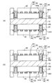
本発明の実施形態を説明する前に、本発明に関連する関連技術の問題点について説明する。図1及び図2は関連技術の配線基板の製造方法を示す断面図である。
(Related technology)
Prior to describing embodiments of the present invention, problems of related technologies related to the present invention will be described. 1 and 2 are cross-sectional views showing a related art method for manufacturing a wiring board.
関連技術の配線基板の製造方法では、図1(a)に示すように、第1配線層200を備えたコア基板100を用意する。第1配線層200の表面には密着増強処理層210が形成されている。密着増強処理層210は、第1配線層200の表面を黒化処理するなどして粗化することによって得られる。
In the related art wiring board manufacturing method, as shown in FIG. 1A, a
コア基板100にはその厚み方向に貫通する貫通電極120が設けられており、コア基板100の上面側の配線層200は貫通電極120を介して下面側の配線層(不図示)に接続されている。コア基板100の両面側に多層配線が形成されるが、以下の説明では上面側のみを参照して説明する。
The
同じく図1(a)に示すように、コア基板100の上に第1配線層200を被覆する樹脂層300を形成する。第1配線層200の表面に密着増強処理層210が形成されているため、樹脂層300は第1配線層200の上に密着性がよい状態で形成される。
Similarly, as shown in FIG. 1A, a
次いで、図1(b)に示すように、レーザによって樹脂層300を加工することにより、第1配線層200に到達するビアホールVHを形成する。このとき、ビアホールVHの底部に樹脂スミアRSが発生する。
Next, as shown in FIG. 1B, the via hole VH reaching the
次いで、図1(c)に示すように、過マンガン酸カリウム法などのデスミア処理によってビアホールVH内の樹脂スミアRSを除去してクリーニングする。このとき、デスミア処理によってビアホールの下部の樹脂層300が外側にエッチングされやすい傾向があり、下部にえぐれ部Aが形成されてしまう。
Next, as shown in FIG. 1C, the resin smear RS in the via hole VH is removed and cleaned by a desmear process such as a potassium permanganate method. At this time, the
さらに、図1(d)に示すように、ビアホールVH内を希硫酸などで酸洗浄することにより、ビアホールVH内に露出する密着増強処理層210を除去して第1配線層200を露出させる。酸洗浄を行うことによって、ビアホールVHの下部のえぐれ部Aがさらに広がった状態となる。
Further, as shown in FIG. 1D, the inside of the via hole VH is acid cleaned with dilute sulfuric acid or the like, thereby removing the adhesion enhancing
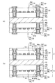
続いて、図2(a)に示すように、スパッタ法により、前処理として逆スパッタを行って第1配線層200の表面を活性化した後に、樹脂層300上及びビアホールVH内に膜厚が0.1μm程度のシード層420を形成する。スパッタ法は成膜のステップカバレジ(被覆性)が悪いため、シード層420はビアホールVHのえぐれ部Aにはほとんど形成されず、ビアホールVHの上部の側面及び底部のみに形成される。
Subsequently, as shown in FIG. 2A, after the reverse sputtering is performed as a pretreatment by the sputtering method to activate the surface of the
なお、無電解めっきによって膜厚が1μm程度のシード層を形成する場合は、ビアホールVHのえぐれ部Aの側面にもシード層が成膜される。 Note that when a seed layer having a thickness of about 1 μm is formed by electroless plating, the seed layer is also formed on the side surface of the bottom portion A of the via hole VH.
本実施形態では、第2配線層の微細化を達成するため、スパッタ法によって薄膜のシード層420を形成するようにしている。シード層420の膜厚を薄くすることにより、後述する金属めっき層をマスクにしてシード層420をエッチングする際にエッチング量を減らすことができるので、第2配線層の微細化を達成できるからである。
In the present embodiment, a
次いで、図2(b)に示すように、第2配線層が配置される部分に開口部320aが設けられためっきレジスト320をフォトリソグラフィによってシード層420の上に形成する。
Next, as shown in FIG. 2B, a plating resist 320 provided with an
さらに、図2(c)に示すように、シード層420をめっき給電経路に利用する電解めっきにより、ビアホールVH内及びめっきレジスト320の開口部320aに銅などからなる金属めっき層440を形成する。
Further, as shown in FIG. 2C, a
このとき、ビアホールVHの下部のえぐれ部Aの側面にはシード層420が存在しないので、えぐれ部Aには電解めっきが施されない。その結果、ビアホールVHのストレート形状の領域は金属めっき層440で充填されるが、下部のえぐれ部AはボイドB(空間)となってしまう。
At this time, since the
次いで、図2(d)に示すように、めっきレジスト320を除去した後に、金属めっき層440をマスクにしてシード層420をエッチングする。これにより、シード層420及び金属めっき層440によって構成される第2配線層400が樹脂層300の上に形成される。第2配線層400はビアホールVH(ビア導体)を介して第1配線層200に接続される。
Next, as shown in FIG. 2D, after the plating resist 320 is removed, the
前述したように、セミアディティブ法で使用されるシード層420をスパッタ法によって薄膜で形成することにより、シード層420のエッチング量を減らすことができるので、第2配線層400の微細化を達成できる。
As described above, since the
しかしながら、ビアホールVHを形成した後にデスミア処理や酸洗浄を行うとビアホールVHの下部に金属めっき層440が充填されないボイドBが形成されてしまうので、配線基板の信頼性を確保できない問題がある。
However, if the desmear process or the acid cleaning is performed after the via hole VH is formed, the void B that is not filled with the
本願発明者は前述した問題を鑑み、デスミア処理せずにビアホール内に樹脂スミアを残した状態で、スパッタ法でシード層を形成し、ビアホールを埋め込む配線層を得た後に、ビアホールの底部を露出させて樹脂スミアを除去する方法を考案した。 In view of the above-mentioned problems, the present inventor formed a seed layer by sputtering while leaving a resin smear in the via hole without performing desmear treatment, and after obtaining a wiring layer for embedding the via hole, the bottom of the via hole was exposed. And devised a method for removing resin smear.
(第1の実施の形態)
図3〜図9は本発明の第1実施形態の配線基板の製造方法を示す断面図、図10は図9(b)の配線基板に半導体チップが実装された様子を示す断面図である。
(First embodiment)
3 to 9 are cross-sectional views showing a method of manufacturing a wiring board according to the first embodiment of the present invention, and FIG. 10 is a cross-sectional view showing a state in which a semiconductor chip is mounted on the wiring board of FIG.
第1実施形態の配線基板の製造方法では、図3(a)に示すように、まず、仮基板10の両面側にエポキシ樹脂やポリイミド樹脂などの樹脂フィルムを貼付するなどして第1樹脂層20をそれぞれ形成する。仮基板10は、その上にビルドアップ配線を形成した後に、ビルドアップ配線から容易に分離できるようになっている。
In the method for manufacturing a wiring board according to the first embodiment, as shown in FIG. 3A, first, a first resin layer is formed by sticking a resin film such as an epoxy resin or a polyimide resin on both sides of the
例えば、仮基板10の両面側には離型処理(シリコーン処理など)が施されており、ビルドアップ配線との界面から仮基板10を分離することができる。
For example, a release treatment (silicone treatment or the like) is performed on both surfaces of the
あるいは、仮基板10の上に銅箔(不図示)の周縁側のみを接着剤で接着し、銅箔の上にビルドアップ配線を形成してもよい。この場合は、仮基板10の接着剤の内側部分を切断することにより、銅箔及びビルドアップ配線を仮基板10から分離することができる。
Or only the peripheral side of copper foil (not shown) may be adhere | attached on the temporary board |
次いで、図3(b)に示すように、両面側の第1樹脂層20をレーザによって加工することにより、仮基板10に到達する第1ビアホールVH1をそれぞれ形成する。このとき、第1ビアホールVH1内に樹脂スミアRSが発生する。
Next, as shown in FIG. 3B, the first via holes VH1 reaching the
本実施形態では、前述した関連技術と違って、第1ビアホールVH1にえぐれ部が形成されないように、デスミア処理を省略する。デスミア処理を省略することにより、第1ビアホールVH1はレーザで加工された直後の形状が維持される。 In the present embodiment, unlike the related technology described above, the desmear process is omitted so that no hollow portion is formed in the first via hole VH1. By omitting the desmear process, the shape of the first via hole VH1 immediately after being processed by the laser is maintained.
つまり、第1ビアホールVH1は、ストレート形状又は上側から下側になるにつれて径が小さくなる順テーパ形状に維持される。また、第1樹脂層20の下には接続すべく配線層が存在しないことから、酸洗浄をさらに省略できるので、第1ビアホールVH1の上記形状が維持される。
That is, the first via hole VH1 is maintained in a straight shape or a forward tapered shape whose diameter decreases from the upper side to the lower side. Further, since there is no wiring layer to be connected under the
次いで、図3(c)に示すように、仮基板10の両面側において、第1ビアホールVH1内に樹脂スミアRSを残した状態で、スパッタ法により、前処理として逆スパッタを行った後に、第1ビアホールVH1内及び第1樹脂層20の上にシード層32をそれぞれ形成する。シード層32としては、ニッケル(Ni)層、クロム(Cr)層又はチタン(Ti)層などが使用される。
Next, as shown in FIG. 3C, after performing reverse sputtering as a pretreatment by the sputtering method with the resin smear RS left in the first via hole VH1 on both sides of the
本実施形態では、第1ビアホールVH1にえぐれ部が形成されないので、スパッタ法により、第1ビアホールVH1の底部から側面全体にわたって薄膜(膜厚:0.1μm程度)のシード層32を成膜することができる。 In the present embodiment, since no hollow portion is formed in the first via hole VH1, a thin seed layer 32 (film thickness: about 0.1 μm) is formed from the bottom of the first via hole VH1 to the entire side surface by sputtering. Can do.
このようにして、第1ビアホールVH1の底部の樹脂スミアRSは、仮基板10とシード層32とによって挟まれた状態となる。
Thus, the resin smear RS at the bottom of the first via hole VH1 is sandwiched between the
本実施形態と違って、第1ビアホールVHを形成した後に、デスミア処理や酸洗浄を行うと第1樹脂層20の表面がエッチングされてその中に含まれるフィラー(シリカ粒子)が露出する。フィラーは、第1樹脂層20の熱膨張率を調整するために添加される。スパッタ法で形成されるシード層32は、第1樹脂層20の表面にフィラーが露出して表面改質されていると密着性が悪くなる傾向がある。
Unlike the present embodiment, after the first via hole VH is formed, when the desmear process or the acid cleaning is performed, the surface of the
デスミア処理や酸洗浄を省略することは、スパッタ法で形成されるシード層32と第1樹脂層20との密着性を向上させるという観点からも都合がよい。
Omitting the desmear treatment and the acid cleaning is also convenient from the viewpoint of improving the adhesion between the
次いで、図4(a)に示すように、コア基板10の両面側において、第1配線層が配置される部分に開口部12aが設けられためっきレジスト12をシード層32の上にそれぞれ形成する。めっきレジスト12の開口部12aは第1ビアホールVH1に連通して配置される。
Next, as shown in FIG. 4A, on both sides of the
さらに、図4(b)に示すように、シード層32をめっき給電経路に利用する電解めっきにより、第1ビアホールVH1内及びめっきレジスト12の開口部12aに銅などからなる金属めっき層34を形成する。
Further, as shown in FIG. 4B, a
このとき、第1ビアホールVH1の内面全体がシード層32で被覆されているので、金属めっき層34はボイドが発生することなく、第1ビアホールVH1に安定して充填される。
At this time, since the entire inner surface of the first via hole VH1 is covered with the
次いで、図5(a)に示すように、仮基板10の両面側において、めっきレジスト12を除去することによりその下のシード層32を露出させる。
Next, as shown in FIG. 5A, the
さらに、図5(b)に示すように、仮基板10の両面側において、金属めっき層34をマスクにしてシード層32をそれぞれエッチングする。これにより、両面側の第1樹脂層20の上に、シード層32及び金属めっき層34によって構成される第1配線層30がそれぞれ形成される。
Further, as shown in FIG. 5B, the
本実施形態では、第1配線層30を構成するシード層32はスパッタ法によって薄膜(0.1μm程度)で形成することができる。このため、無電解めっきで厚膜(1μm程度)のシード層を形成する場合より、シード層32をエッチングする際の第1配線層30の細りが低減されると共に、微細化する際のパターン飛びの発生が防止される。
In the present embodiment, the
さらには、デスミア処理を省略することにより第1樹脂層20の表面が粗化されないため、シード層32のエッチング残渣が発生しにくくなり、微細な第1配線層30を歩留りよく形成することができる。本実施形態では、第1配線層30の配線ピッチを30μm以下(ライン:スペース=15:15μm以下)に微細化して形成することができる。
Furthermore, since the surface of the
次いで、図6(a)に示すように、仮基板10の両面側において、第1樹脂層20及び第1配線層30の上に樹脂フィルムを貼付するなどして第2樹脂層40をそれぞれ形成する。さらに、両面側の第2樹脂層40をレーザで加工することにより、第1配線層30に到達する第2ビアホールVH2をそれぞれ形成する。第2ビアホールVH2を形成する際にも底部に樹脂スミアRSが発生する。
Next, as shown in FIG. 6A, the
第2ビアホールVH2は第1配線層30に接続する必要があるので、第2ビアホールVH2内の樹脂スミアRSを除去する必要がある。
Since the second via hole VH2 needs to be connected to the
このため、図6(b)に示すように、第2ビアホールVH2内をデスミア処理することにより樹脂スミアRSを除去してクリーニングする。さらに、第2ビアホールVH2内を酸洗浄する。これにより、第2ビアホールVH2の下部にえぐれ部Aが発生する。第2配線層は第1配線層30より配線ピッチ(ライン:スペース)が広く設定されるため、無電解めっきによる厚膜のシード層52を使用することができる。
Therefore, as shown in FIG. 6B, the resin smear RS is removed and cleaned by desmearing the inside of the second via hole VH2. Further, the inside of the second via hole VH2 is acid cleaned. As a result, a hollow portion A is generated below the second via hole VH2. Since the second wiring layer has a wider wiring pitch (line: space) than the
次いで、図7(a)に示すように、無電解めっきで形成されたシード層52及び金属めっき層54によって構成される第2配線層50を第2樹脂層40の上に形成する。第2配線層50は第2ビアホールVH2(ビア導体)を介して第1配線層30に電気接続される。
Next, as shown in FIG. 7A, the
形成過程を詳しく説明すると、第2ビアホールVH2内及び第2樹脂層40の上に無電解めっきによってシード層52を形成する。このとき、無電解めっきによって形成されるシード層52は第2ビアホールVH2のえぐれ部Aの側面を被覆して形成される。
The formation process will be described in detail. The
その後に、第1配線層30の形成方法と同様に、第2配線層50が配置される部分に開口部が設けられためっきレジスト(不図示)を形成する。さらに、電解めっきによって第2ビアホールVH2内及びめっきレジストの開口部に金属めっき層54を形成する。
Thereafter, in the same manner as the method for forming the
第2ビアホールVH2のえぐれ部Aはシード層52で被覆されているので、金属めっき層54はボイドが発生することなく第2ビアホールVH2内に充填される。その後に、めっきレジストを除去した後に、金属めっき層54をマスクにしてシード層52をエッチングする。
Since the hollow portion A of the second via hole VH2 is covered with the
これにより、第1配線層30と第2配線層50との接続部に樹脂スミアRSが残ることなく、第1配線層30と第2配線層50とが信頼性よく電気接続される。
Accordingly, the resin wiring smear RS does not remain at the connection portion between the
続いて、図7(b)に示すように、コア基板10の両面側において、第2配線層50のパッド部上に開口部14aが設けられたソルダレジスト14を第2樹脂層40の上にそれぞれ形成する。
Subsequently, as shown in FIG. 7B, the solder resist 14 provided with the
これにより、仮基板10の両面側にビルドアップ配線2がそれぞれ形成される。
As a result, the build-up
本実施形態では、第1配線層30の上に第2配線層50を積層する形態を例示するが、積層数は任意に設定することができ、第1配線層30に接続されるn層(nは1以上の整数)の上側配線層を積層してもよい。
In the present embodiment, an example in which the
また、第2配線層50を含む上側配線層の形成方法としては、前述したセミアディティブ法の他に、サブトラクティブ法などを使用してもよい。
Further, as a method for forming the upper wiring layer including the
次いで、図8に示すように、仮基板10とビルドアップ配線2の第1樹脂層20との界面から剥離することにより、仮基板10とビルドアップ配線2とを分離する。このとき、ビルドアップ配線2の第1樹脂層20の露出面に第1ビアホールVH1の底部に残った樹脂スミアRSが露出した状態となる。
Next, as shown in FIG. 8, the
あるいは、前述したように、仮基板10の上に銅箔の周縁側のみを接着剤で接着し、銅箔の上にビルドアップ配線2を形成する場合は、仮基板10の接着剤の内側部分を切断することにより、銅箔及びビルドアップ配線2が仮基板10から分離される。この場合は、銅箔がウェットエッチングによってビルドアップ配線2から除去されて、樹脂スミアが露出する。
Alternatively, as described above, when only the peripheral side of the copper foil is bonded onto the
あるいは、仮基板10を銅などの金属板や金属箔から形成し、横方向から仮基板10をウェットエッチングすることによりビルドアップ配線2を分離することも可能である。
Alternatively, the build-up
次いで、図9(a)に示すように、図8のビルドアップ配線2の露出面の樹脂スミアRSをデスミア処理によって除去する。これにより、第1ビアホールVH1の底部(図9(a)では上部)のシード層32が露出する。デスミア処理の他に、ドライエッチング又はCMP(Chemical Mechanical Polishing)などによって樹脂スミアRSを除去してもよい。
Next, as shown in FIG. 9A, the resin smear RS on the exposed surface of the build-up
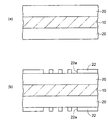
その後に、図9(b)に示すように、第1ビアホールVH1の底部(図9(b)では上部)のシード層32をエッチングによって除去することにより、第1配線層30の金属めっき層(銅)34を露出させる。
Thereafter, as shown in FIG. 9B, the
さらに、露出した金属めっき層34の上にニッケル(Ni)/金(Au)めっき層を順次形成するなどして、半導体チップが接続されるチップ用接続部C1を得る。このとき同時に、ビルドアップ配線2の下面側のソルダレジスト14の開口部14内の第1配線層30にニッケル/金めっき層などからなる端子用接続部C2が形成される。
Further, a nickel (Ni) / gold (Au) plating layer is sequentially formed on the exposed
なお、第1ビアホールVH1の底部(図9(b)では上部)にシード層32を残しても差し支えない場合は、シード層32の上にチップ用接続部Cが形成される。
If the
これにより、第1実施形態の配線基板1が得られる。
Thereby, the
以上説明したように、第1実施形態の配線基板の製造方法では、仮基板10上の第1樹脂層20にレーザによって第1ビアホールVH1が形成される。次いで、デスミア処理や酸洗浄を省略して第1ビアホールVH1内に樹脂スミアを残した状態でスパッタ法によってシード層32が形成される。
As described above, in the wiring board manufacturing method of the first embodiment, the first via hole VH1 is formed in the
デスミア処理や酸洗浄を省略することにより、第1ビアホールVHにはえぐれ部が発生しないので、スパッタ法によって第1ビアホールVH1の内面に薄膜のシード層32を良好なステップカバレジ(被覆性)で形成することができる。
By omitting the desmear process and the acid cleaning, the first via hole VH does not have a void portion, so that the
従って、第1ビアホールVH1内にボイドが発生することなく、信頼性の高い微細な第1配線層30をセミアディティブ法によって形成することができる。
Therefore, the highly reliable fine
第1配線層30の上に配置される第2ビアホールVH2はデスミア処理によって樹脂スミアが除去される。その後に、無電解めっきによるシード層及び電解金属めっき層から第2配線層50が形成されて、ビルドアップ配線2が得られる。第2配線層50は第1配線層30より配線ピッチ(ライン:スペース)が広く設定される。
Resin smear is removed from the second via hole VH2 disposed on the
そして、仮基板10とビルドアップ配線2とが分離された後に、ビルドアップ配線2の露出面の樹脂スミアRSが除去される。
Then, after the
このようにして、第1ビアホールVH1の底部に第1配線層30が露出し、チップ用接続部C1として利用される。第1ビアホールVH1の底部にえぐれ部が発生しないので、狭ピッチのチップ用接続部C1を歩留りよく形成することができる。
In this way, the
これにより、狭ピッチの接続パッドを備えた高性能な半導体チップを実装するための配線基板として使用することができる。 Thereby, it can be used as a wiring board for mounting a high-performance semiconductor chip having connection pads with a narrow pitch.
図10には図9(b)の配線基板1に半導体チップが実装された様子が示されている。図10に示すように、半導体チップ60がはんだなどのバンプ電極62によって配線基板1の第1配線層30のチップ用接続部C1にフリップチップ接続される。
FIG. 10 shows a state in which a semiconductor chip is mounted on the
このとき、チップ用接続部C1は第1樹脂層20と同一面に形成されて平坦化されており、ソルダレジストの段差もないため、半導体チップ60をフリップチップ実装しやすいという利点がある。
At this time, the chip connecting portion C1 is formed on the same surface as the
さらに、半導体チップ60の下側の隙間にアンダーフィル樹脂64が充填される。そして、配線基板1の下面側の第2配線層50の端子用接続部C2にはんだボールなどが搭載されて外部接続端子66が設けられる。
Further, an
(第2の実施の形態)
図11〜図14は本発明の第2実施形態の配線基板の製造方法を示す断面図、図15は図14(b)の配線基板に半導体チップが実装される様子を示す断面図である。第2実施形態では、第1実施形態と同一工程についてはその詳しい説明を省略する。第2実施形態では、第1配線層がダマシンプロセスによって形成される。
(Second Embodiment)
FIGS. 11 to 14 are cross-sectional views showing a method for manufacturing a wiring board according to a second embodiment of the present invention, and FIG. 15 is a cross-sectional view showing how a semiconductor chip is mounted on the wiring board of FIG. In the second embodiment, detailed description of the same steps as those in the first embodiment is omitted. In the second embodiment, the first wiring layer is formed by a damascene process.
第2実施形態の配線基板の製造方法では、図11(a)に示すように、第1実施形態の図3(a)と同様に、仮基板10の両面側に第1樹脂層20をそれぞれ形成する。次いで、図11(b)に示すように、両面側の第1樹脂層20の上に、第1配線層が配置される部分に開口部22aが設けられた永久レジスト22をフォトリソグラフィによって形成する。
In the method of manufacturing the wiring board according to the second embodiment, as shown in FIG. 11A, the first resin layers 20 are respectively formed on both sides of the
永久レジスト22は、めっきレジストとして機能すると共に、それ以降は剥離せずに層間絶縁層として使用される。 The permanent resist 22 functions as a plating resist and thereafter is used as an interlayer insulating layer without peeling off.
次いで、図12(a)に示すように、コア基板10の両面側において、永久レジスト22及び第1樹脂層20をレーザで加工することにより、仮基板10に到達する第1ビアホールVH1をそれぞれ形成する。このとき、第1ビアホールVH1の底部に樹脂スミアRSが発生する。
Next, as shown in FIG. 12A, the first via holes VH1 reaching the
ここで、第1実施形態と同様に、デスミア処理及び酸洗浄が省略される。これにより、図12(a)の第1ビアホールVH1の形状と、永久レジスト22及びその開口部22aの形状が変形することなく維持される。
Here, as in the first embodiment, desmear treatment and acid cleaning are omitted. Thereby, the shape of the first via hole VH1 in FIG. 12A and the shapes of the permanent resist 22 and the
本実施形態と違って、図12(a)において第1ビアホールVH1内の樹脂スミアRSをデスミア処理で除去する場合について言及する。 Unlike the present embodiment, the case where the resin smear RS in the first via hole VH1 is removed by desmear processing in FIG.
この場合は、第1ビアホールVH1の下部にえぐれ部が発生するばかりではなく、永久レジスト22が極端に細ったり、パターン飛びが発生したりするので、めっきレジストとして機能しなくなることが理解される。 In this case, it is understood that not only does a hollow portion occur in the lower portion of the first via hole VH1, but the permanent resist 22 becomes extremely thin or pattern skipping occurs, so that it does not function as a plating resist.
また、デスミア処理による永久レジスト22のダメージを回避するために、第1樹脂層20に第1ビアホールVH1を形成し、デスミア処理した後に、永久レジスト22をパターン化する方法が考えられる。
In order to avoid the damage of the permanent resist 22 due to the desmear process, a method of patterning the permanent resist 22 after forming the first via hole VH1 in the
しかしながら、第1ビアホールVH1の段差が発生した第1樹脂層20の上に永久レジスト22をパターン精度よく形成することは困難を極める。
However, it is extremely difficult to form the permanent resist 22 with high pattern accuracy on the
続いて、図12(b)に示すように、仮基板10の両面側において、第1ビアホールVH1内に樹脂スミアRSを残した状態で、スパッタ法により、前処理として逆スパッタを行った後に、第1ビアホールVH1内、第1樹脂層20及び永久レジスト22の上にシード層32を形成する。これにより、仮基板10とシード層32との間に樹脂スミアRSが挟まれた状態となる。
Subsequently, as shown in FIG. 12B, on the both sides of the
続いて、図13(a)に示すように、仮基板10の両面側において、シード層32をめっき給電経路に利用する電解めっきにより、第1ビアホールVH1内及び永久レジスト22の開口部を埋め込む金属めっき層34をそれぞれ形成する。
Subsequently, as shown in FIG. 13A, on both sides of the
次いで、図13(b)に示すように、両面側の金属めっき層34及びシード層32を永久レジスト22が露出するまでCMPなどでそれぞれ研磨する。これにより、第1ビアホールVH1内及び永久レジスト22の開口部にシード層32及び金属めっき層34から構成される第1配線層30が埋め込まれて形成される。
Next, as shown in FIG. 13B, the
第2実施形態では、第1ビアホールVH1及び永久レジスト22のパターン形状が変形しないので、設計スペック内の寸法精度のよい第1配線層30が形成される。
In the second embodiment, since the pattern shapes of the first via hole VH1 and the permanent resist 22 are not deformed, the
続いて、図14(a)に示すように、第1実施形態の図6(a)〜図7(b)と同一の工程を遂行する。これにより、第2ビアホールVH2(ビア導体)を介して第1配線層30に接続される第2配線層50が第2樹脂層40の上に形成される。第2配線層50はシード層52及び金属めっき層54によって構成される。
Subsequently, as shown in FIG. 14A, the same steps as those in FIGS. 6A to 7B of the first embodiment are performed. Thereby, the
第1実施形態と同様に、第2樹脂層40に形成された第2ビアホールVH2内に発生する樹脂スミアがデスミア処理で除去されることにより、第2ビアホールVH2の下部にえぐれ部Aが形成される。そして、第2配線層50を構成するシード層52は無電解めっきによって形成される。
Similar to the first embodiment, the resin smear generated in the second via hole VH2 formed in the
さらに、仮基板10の両面側において、第2配線層50のパッド部上に開口部14aが設けられたソルダレジスト14がそれぞれ形成される。
Further, on both sides of the
このようにして、仮基板10の両面側にビルドアップ配線2がそれぞれ形成される。
In this way, the build-up
第1実施形態と同様に、第1配線層30に接続されるn層(nは1以上の整数)の上側配線層を積層してもよい。また、第2配線層50を含む上側配線層の形成方法としては、前述したセミアディティブ法の他に、サブトラクティブ法などを使用してもよい。
Similarly to the first embodiment, an upper wiring layer of n layers (n is an integer of 1 or more) connected to the
次いで、図14(b)に示すように、第1実施形態と同様に、仮基板10とビルドアップ配線2とを分離することにより、ビルドアップ配線2の第1樹脂層20の露出面に樹脂スミアRSを露出させる。
Next, as shown in FIG. 14B, as in the first embodiment, the
さらに、図15(a)に示すように、ビルドアップ配線2の第1樹脂層20の露出面をデスミア処理する。これにより、樹脂スミアRSが除去されて第1ビアホールVH1の底部(図15(a)では上部)の第1配線層30のシード層32を露出させる。
Further, as shown in FIG. 15A, the exposed surface of the
続いて、図15(b)に示すように、ビルドアップ配線2の第1樹脂層20の露出面に露出するシード層32をエッチングして金属めっき層34を露出させ、その上にNi/Auめっき層を形成するなどしてチップ用接続部C1を得る。なお、第1ビアホールVH1の底部(図15(b)では上部)にシード層32を残しても差し支えない場合は、シード層32の上にチップ用接続部Cが形成される。
Subsequently, as shown in FIG. 15B, the
また同時に、ビルドアップ配線2のソルダレジスト14の開口部14内の第2配線層50にNi/Auめっき層などの端子用接続部C2が形成される。これにより、第2実施形態の配線基板1aが得られる。
At the same time, a terminal connection portion C2 such as a Ni / Au plating layer is formed in the
第2実施形態の配線基板の製造方法は、第1実施形態と同様な効果を奏する。第2実施形態では、ダマシンプロセスを使用するので、第1ビアホールVH1及び永久レジスト22の開口部22aに対応して第1配線層30が形成される。第1実施形態で説明したセミアディティブ法と違って、シード層32のエッチング工程がないので、第1実施形態より第1配線層30の微細化を図ることができる。
The method for manufacturing a wiring board according to the second embodiment has the same effects as those of the first embodiment. In the second embodiment, since a damascene process is used, the
そして、図16に示すように、第1実施形態と同様に、配線基板1aのチップ用接続部Cに半導体チップ60がはんだなどのバンプ電極62によってフリップチップ接続される。また、半導体チップ60の下側の隙間にアンダーフィル樹脂64が充填される。
Then, as shown in FIG. 16, as in the first embodiment, the
さらに、配線基板1aの端子用接続部C2にはんだボールを搭載するなどして外部接続端子66が設けられる。
Furthermore,
なお、前述した第1、第2実施形態では、仮基板10の両面側にビルドアップ配線2をそれぞれ形成しているが、仮基板10の片面上のみにビルドアップ配線2を形成することにより、配線基板1,1aを製造してもよい。
In the first and second embodiments described above, the build-up
1,1a…配線基板、2…ビルドアップ配線、10…仮基板、12…めっきレジスト、12a,14a,22a…開口部、14…ソルダレジスト、20…第1樹脂層、22…永久レジスト、30…第1配線層、32,52…シード層、34,54…金属めっき層、40…第2樹脂層、50…第2配線層、60…半導体チップ、62…バンプ電極、64…アンダーフィル樹脂、66…外部接続端子、A…えぐれ部、B…ボイド(空間)、RS…樹脂スミア、VH1…第1ビアホール、VH2…第2ビアホール。
DESCRIPTION OF
Claims (7)
前記樹脂層をレーザで貫通加工することにより、前記仮基板に到達するビアホールを形成する工程と、
前記樹脂層上及び前記ビアホールの内面にシード層を形成する工程と、
前記シード層と、前記シード層をめっき給電経路に利用する電解めっきで形成される金属めっき層とを利用することにより、前記ビアホールに充填される配線層を得る工程と、
前記仮基板と前記樹脂層とを分離することにより、前記樹脂層の露出面に前記ビアホールの底部の前記配線層上に残った樹脂スミアを露出させる工程と、
前記樹脂スミアを露出させる工程の後に、前記ビアホールの底部の前記配線層上の前記樹脂スミアを除去する工程とを有することを特徴とする配線基板の製造方法。 Forming a resin layer in a state where it can be separated on the temporary substrate;
Forming a via hole reaching the temporary substrate by penetrating the resin layer with a laser; and
Forming a seed layer on the resin layer and on the inner surface of the via hole;
Obtaining a wiring layer filling the via hole by using the seed layer and a metal plating layer formed by electrolytic plating using the seed layer as a plating power feeding path;
Separating the temporary substrate and the resin layer to expose the resin smear remaining on the wiring layer at the bottom of the via hole on the exposed surface of the resin layer;
After said step of exposing the resin smear, method for manufacturing a wiring substrate, characterized by a step of removing the resin smear on the wiring layer at the bottom of the via hole.
前記シード層の上に、前記配線層が配置される部分に開口部が設けられためっきレジストを形成する工程と、
前記ビアホール内及び前記めっきレジストの開口部に前記金属めっき層を形成する工程と、
前記めっきレジストを除去する工程と、
前記金属めっき層をマスクにして前記シード層をエッチングする工程とを含むことを特徴とする請求項1に記載の配線基板の製造方法。 The step of obtaining the wiring layer includes
Forming a plating resist having an opening in a portion where the wiring layer is disposed on the seed layer;
Forming the metal plating layer in the via hole and in the opening of the plating resist;
Removing the plating resist;
The method according to claim 1, further comprising: etching the seed layer using the metal plating layer as a mask.
前記樹脂層の上に、開口部が設けられた永久レジストを形成することを含み、
前記ビアホールを形成する工程において、
前記永久レジスト及び前記樹脂層を貫通する前記ビアホールを形成し、
前記シード層を形成する工程において、
前記シード層が前記永久レジストの上にさらに形成され、
前記配線層を得る工程は、
前記ビアホール内及び前記永久レジストの開口部を埋め込むように前記金属めっき層を形成する工程と、
前記金属めっき層及びシード層を前記永久レジストが露出するまで研磨することにより、前記ビアホール内及び前記永久レジストの開口部に前記配線層を得る工程とを含むことを特徴とする請求項1に記載の配線基板の製造方法。 The step of forming the resin layer includes
Forming a permanent resist provided with openings on the resin layer;
In the step of forming the via hole,
Forming the via hole penetrating the permanent resist and the resin layer;
In the step of forming the seed layer,
The seed layer is further formed on the permanent resist;
The step of obtaining the wiring layer includes
Forming the metal plating layer so as to fill the via hole and the opening of the permanent resist;
2. The step of polishing the metal plating layer and the seed layer until the permanent resist is exposed to obtain the wiring layer in the via hole and in the opening of the permanent resist. Wiring board manufacturing method.
前記配線層の上にそれに電気接続されるn層(nは1以上の整数)の上側配線層を形成する工程をさらに有することを特徴とする請求項1乃至3のいずれか一項に記載の配線基板の製造方法。 After the step of obtaining the wiring layer and before the step of separating the temporary substrate and the resin layer,
4. The method according to claim 1, further comprising forming an upper wiring layer of n layers (n is an integer of 1 or more) electrically connected to the wiring layer. 5. A method for manufacturing a wiring board.
Priority Applications (1)
| Application Number | Priority Date | Filing Date | Title |
|---|---|---|---|
| JP2009180388A JP5419583B2 (en) | 2009-08-03 | 2009-08-03 | Wiring board manufacturing method |
Applications Claiming Priority (1)
| Application Number | Priority Date | Filing Date | Title |
|---|---|---|---|
| JP2009180388A JP5419583B2 (en) | 2009-08-03 | 2009-08-03 | Wiring board manufacturing method |
Publications (3)
| Publication Number | Publication Date |
|---|---|
| JP2011035182A JP2011035182A (en) | 2011-02-17 |
| JP2011035182A5 JP2011035182A5 (en) | 2012-08-09 |
| JP5419583B2 true JP5419583B2 (en) | 2014-02-19 |
Family
ID=43763960
Family Applications (1)
| Application Number | Title | Priority Date | Filing Date |
|---|---|---|---|
| JP2009180388A Active JP5419583B2 (en) | 2009-08-03 | 2009-08-03 | Wiring board manufacturing method |
Country Status (1)
| Country | Link |
|---|---|
| JP (1) | JP5419583B2 (en) |
Families Citing this family (2)
| Publication number | Priority date | Publication date | Assignee | Title |
|---|---|---|---|---|
| KR20150024093A (en) * | 2013-08-26 | 2015-03-06 | 삼성전기주식회사 | Printed circuit board and method of manufacturing the same |
| EP3833165A4 (en) | 2018-07-31 | 2022-05-04 | Kyocera Corporation | Printed-wiring board and method of manufacturing printed-wiring board |
Family Cites Families (7)
| Publication number | Priority date | Publication date | Assignee | Title |
|---|---|---|---|---|
| JP3790063B2 (en) * | 1999-03-08 | 2006-06-28 | 新光電気工業株式会社 | Multilayer wiring board, manufacturing method thereof, and semiconductor device |
| JP2001044589A (en) * | 1999-07-30 | 2001-02-16 | Nitto Denko Corp | Circuit board |
| JP2001267747A (en) * | 2000-03-22 | 2001-09-28 | Nitto Denko Corp | Manufacturing method for multi-layered circuit board |
| JP4448610B2 (en) * | 2000-10-18 | 2010-04-14 | 日東電工株式会社 | Circuit board manufacturing method |
| JP2004193520A (en) * | 2002-12-13 | 2004-07-08 | Sumitomo Bakelite Co Ltd | Manufacturing method of printed circuit board |
| JP2005109108A (en) * | 2003-09-30 | 2005-04-21 | Ibiden Co Ltd | Build-up printed wiring board and manufacturing method thereof |
| JP2006049804A (en) * | 2004-07-07 | 2006-02-16 | Shinko Electric Ind Co Ltd | Manufacturing method of wiring board |
-
2009
- 2009-08-03 JP JP2009180388A patent/JP5419583B2/en active Active
Also Published As
| Publication number | Publication date |
|---|---|
| JP2011035182A (en) | 2011-02-17 |
Similar Documents
| Publication | Publication Date | Title |
|---|---|---|
| JP5101169B2 (en) | Wiring board and manufacturing method thereof | |
| TWI437668B (en) | Wiring board, semiconductor device, method of fabricating wiring board and method of fabricating semiconductor device | |
| JP5820673B2 (en) | Semiconductor device and manufacturing method thereof | |
| US20080308308A1 (en) | Method of manufacturing wiring board, method of manufacturing semiconductor device and wiring board | |
| JP4980295B2 (en) | Wiring substrate manufacturing method and semiconductor device manufacturing method | |
| WO2004103039A1 (en) | Double-sided wiring board, double-sided wiring board manufacturing method, and multilayer wiring board | |
| KR101077380B1 (en) | A printed circuit board and a fabricating method the same | |
| JP2014154800A (en) | Wiring board and manufacturing method thereof | |
| WO2004014114A1 (en) | Method for manufacturing board with built-in device and board with built-in device, and method for manufacturing printed wiring board and printed wiring board | |
| JP4452650B2 (en) | Wiring board and manufacturing method thereof | |
| US9711476B2 (en) | Wiring board and electronic component device | |
| JPWO2009118925A1 (en) | Electronic component built-in wiring board and manufacturing method thereof | |
| TW201136466A (en) | Multilayer wiring substrate | |
| JP5221887B2 (en) | Wiring board manufacturing method | |
| JP2010171387A (en) | Circuit board structure and production method therefor | |
| JP4170266B2 (en) | Wiring board manufacturing method | |
| JP2006196768A (en) | Method of manufacturing wiring board | |
| US9137896B2 (en) | Wiring substrate | |
| JP6092555B2 (en) | Wiring board manufacturing method | |
| JP3981227B2 (en) | Multilayer wiring board and manufacturing method thereof | |
| JP5419583B2 (en) | Wiring board manufacturing method | |
| JP2006245213A (en) | Manufacturing method of wiring circuit board | |
| JP4975581B2 (en) | Wiring board and manufacturing method thereof | |
| JP4549695B2 (en) | Wiring board manufacturing method | |
| JP2008227538A (en) | Method for fabricating wiring board and the same |
Legal Events
| Date | Code | Title | Description |
|---|---|---|---|
| A521 | Written amendment |
Free format text: JAPANESE INTERMEDIATE CODE: A523 Effective date: 20120622 |
|
| A621 | Written request for application examination |
Free format text: JAPANESE INTERMEDIATE CODE: A621 Effective date: 20120622 |
|
| A977 | Report on retrieval |
Free format text: JAPANESE INTERMEDIATE CODE: A971007 Effective date: 20130417 |
|
| A131 | Notification of reasons for refusal |
Free format text: JAPANESE INTERMEDIATE CODE: A131 Effective date: 20130423 |
|
| TRDD | Decision of grant or rejection written | ||
| A01 | Written decision to grant a patent or to grant a registration (utility model) |
Free format text: JAPANESE INTERMEDIATE CODE: A01 Effective date: 20131112 |
|
| A61 | First payment of annual fees (during grant procedure) |
Free format text: JAPANESE INTERMEDIATE CODE: A61 Effective date: 20131119 |
|
| R150 | Certificate of patent or registration of utility model |
Ref document number: 5419583 Country of ref document: JP Free format text: JAPANESE INTERMEDIATE CODE: R150 |