JP2014154800A - Wiring board and manufacturing method thereof - Google Patents
Wiring board and manufacturing method thereof Download PDFInfo
- Publication number
- JP2014154800A JP2014154800A JP2013025210A JP2013025210A JP2014154800A JP 2014154800 A JP2014154800 A JP 2014154800A JP 2013025210 A JP2013025210 A JP 2013025210A JP 2013025210 A JP2013025210 A JP 2013025210A JP 2014154800 A JP2014154800 A JP 2014154800A
- Authority
- JP
- Japan
- Prior art keywords
- layer
- wiring
- insulating layer
- via hole
- wiring board
- Prior art date
- Legal status (The legal status is an assumption and is not a legal conclusion. Google has not performed a legal analysis and makes no representation as to the accuracy of the status listed.)
- Pending
Links
- 238000004519 manufacturing process Methods 0.000 title claims description 30
- 229910052751 metal Inorganic materials 0.000 claims abstract description 64
- 239000002184 metal Substances 0.000 claims abstract description 64
- 238000007747 plating Methods 0.000 claims abstract description 52
- 239000004020 conductor Substances 0.000 claims abstract description 18
- 239000000758 substrate Substances 0.000 claims description 22
- 238000001312 dry etching Methods 0.000 claims description 14
- 238000009713 electroplating Methods 0.000 claims description 8
- 238000004544 sputter deposition Methods 0.000 claims description 6
- 230000007423 decrease Effects 0.000 claims description 4
- XUIMIQQOPSSXEZ-UHFFFAOYSA-N Silicon Chemical compound [Si] XUIMIQQOPSSXEZ-UHFFFAOYSA-N 0.000 abstract description 31
- 229910052710 silicon Inorganic materials 0.000 abstract description 31
- 239000010703 silicon Substances 0.000 abstract description 31
- 239000010410 layer Substances 0.000 description 295
- 239000011229 interlayer Substances 0.000 description 75
- 238000000034 method Methods 0.000 description 32
- 239000004065 semiconductor Substances 0.000 description 20
- 239000010949 copper Substances 0.000 description 14
- RYGMFSIKBFXOCR-UHFFFAOYSA-N Copper Chemical compound [Cu] RYGMFSIKBFXOCR-UHFFFAOYSA-N 0.000 description 13
- 229910052802 copper Inorganic materials 0.000 description 12
- 238000001039 wet etching Methods 0.000 description 8
- 229920005989 resin Polymers 0.000 description 7
- 239000011347 resin Substances 0.000 description 7
- 238000000206 photolithography Methods 0.000 description 6
- PXHVJJICTQNCMI-UHFFFAOYSA-N Nickel Chemical compound [Ni] PXHVJJICTQNCMI-UHFFFAOYSA-N 0.000 description 5
- 239000000654 additive Substances 0.000 description 5
- 239000000853 adhesive Substances 0.000 description 5
- 230000001070 adhesive effect Effects 0.000 description 5
- 239000010408 film Substances 0.000 description 4
- 239000010931 gold Substances 0.000 description 4
- 229910000679 solder Inorganic materials 0.000 description 4
- 239000010936 titanium Substances 0.000 description 4
- RTAQQCXQSZGOHL-UHFFFAOYSA-N Titanium Chemical compound [Ti] RTAQQCXQSZGOHL-UHFFFAOYSA-N 0.000 description 3
- 238000007772 electroless plating Methods 0.000 description 3
- 238000005530 etching Methods 0.000 description 3
- PCHJSUWPFVWCPO-UHFFFAOYSA-N gold Chemical compound [Au] PCHJSUWPFVWCPO-UHFFFAOYSA-N 0.000 description 3
- 229910052737 gold Inorganic materials 0.000 description 3
- 229910052719 titanium Inorganic materials 0.000 description 3
- 230000015572 biosynthetic process Effects 0.000 description 2
- 238000009616 inductively coupled plasma Methods 0.000 description 2
- 238000009413 insulation Methods 0.000 description 2
- 229910052759 nickel Inorganic materials 0.000 description 2
- 230000002093 peripheral effect Effects 0.000 description 2
- 238000001020 plasma etching Methods 0.000 description 2
- 230000001681 protective effect Effects 0.000 description 2
- QGZKDVFQNNGYKY-UHFFFAOYSA-O Ammonium Chemical compound [NH4+] QGZKDVFQNNGYKY-UHFFFAOYSA-O 0.000 description 1
- ZAMOUSCENKQFHK-UHFFFAOYSA-N Chlorine atom Chemical compound [Cl] ZAMOUSCENKQFHK-UHFFFAOYSA-N 0.000 description 1
- 239000007864 aqueous solution Substances 0.000 description 1
- 229910052801 chlorine Inorganic materials 0.000 description 1
- 239000000460 chlorine Substances 0.000 description 1
- 239000011889 copper foil Substances 0.000 description 1
- ORTQZVOHEJQUHG-UHFFFAOYSA-L copper(II) chloride Chemical compound Cl[Cu]Cl ORTQZVOHEJQUHG-UHFFFAOYSA-L 0.000 description 1
- 238000005260 corrosion Methods 0.000 description 1
- 230000007797 corrosion Effects 0.000 description 1
- 238000001035 drying Methods 0.000 description 1
- 229920006332 epoxy adhesive Polymers 0.000 description 1
- 239000003822 epoxy resin Substances 0.000 description 1
- 239000004744 fabric Substances 0.000 description 1
- 239000011521 glass Substances 0.000 description 1
- 239000007788 liquid Substances 0.000 description 1
- 239000000463 material Substances 0.000 description 1
- 229920000647 polyepoxide Polymers 0.000 description 1
- 229920001721 polyimide Polymers 0.000 description 1
- 239000009719 polyimide resin Substances 0.000 description 1
- 239000010409 thin film Substances 0.000 description 1
Images


Classifications
-
- H—ELECTRICITY
- H01—ELECTRIC ELEMENTS
- H01L—SEMICONDUCTOR DEVICES NOT COVERED BY CLASS H10
- H01L23/00—Details of semiconductor or other solid state devices
- H01L23/48—Arrangements for conducting electric current to or from the solid state body in operation, e.g. leads, terminal arrangements ; Selection of materials therefor
- H01L23/488—Arrangements for conducting electric current to or from the solid state body in operation, e.g. leads, terminal arrangements ; Selection of materials therefor consisting of soldered or bonded constructions
- H01L23/498—Leads, i.e. metallisations or lead-frames on insulating substrates, e.g. chip carriers
- H01L23/49827—Via connections through the substrates, e.g. pins going through the substrate, coaxial cables
-
- H—ELECTRICITY
- H01—ELECTRIC ELEMENTS
- H01L—SEMICONDUCTOR DEVICES NOT COVERED BY CLASS H10
- H01L21/00—Processes or apparatus adapted for the manufacture or treatment of semiconductor or solid state devices or of parts thereof
- H01L21/02—Manufacture or treatment of semiconductor devices or of parts thereof
- H01L21/04—Manufacture or treatment of semiconductor devices or of parts thereof the devices having at least one potential-jump barrier or surface barrier, e.g. PN junction, depletion layer or carrier concentration layer
- H01L21/48—Manufacture or treatment of parts, e.g. containers, prior to assembly of the devices, using processes not provided for in a single one of the subgroups H01L21/06 - H01L21/326
- H01L21/4814—Conductive parts
- H01L21/4846—Leads on or in insulating or insulated substrates, e.g. metallisation
- H01L21/4857—Multilayer substrates
-
- H—ELECTRICITY
- H01—ELECTRIC ELEMENTS
- H01L—SEMICONDUCTOR DEVICES NOT COVERED BY CLASS H10
- H01L21/00—Processes or apparatus adapted for the manufacture or treatment of semiconductor or solid state devices or of parts thereof
- H01L21/02—Manufacture or treatment of semiconductor devices or of parts thereof
- H01L21/04—Manufacture or treatment of semiconductor devices or of parts thereof the devices having at least one potential-jump barrier or surface barrier, e.g. PN junction, depletion layer or carrier concentration layer
- H01L21/48—Manufacture or treatment of parts, e.g. containers, prior to assembly of the devices, using processes not provided for in a single one of the subgroups H01L21/06 - H01L21/326
- H01L21/4814—Conductive parts
- H01L21/4846—Leads on or in insulating or insulated substrates, e.g. metallisation
- H01L21/486—Via connections through the substrate with or without pins
-
- H—ELECTRICITY
- H01—ELECTRIC ELEMENTS
- H01L—SEMICONDUCTOR DEVICES NOT COVERED BY CLASS H10
- H01L21/00—Processes or apparatus adapted for the manufacture or treatment of semiconductor or solid state devices or of parts thereof
- H01L21/70—Manufacture or treatment of devices consisting of a plurality of solid state components formed in or on a common substrate or of parts thereof; Manufacture of integrated circuit devices or of parts thereof
- H01L21/71—Manufacture of specific parts of devices defined in group H01L21/70
- H01L21/768—Applying interconnections to be used for carrying current between separate components within a device comprising conductors and dielectrics
- H01L21/76801—Applying interconnections to be used for carrying current between separate components within a device comprising conductors and dielectrics characterised by the formation and the after-treatment of the dielectrics, e.g. smoothing
- H01L21/76802—Applying interconnections to be used for carrying current between separate components within a device comprising conductors and dielectrics characterised by the formation and the after-treatment of the dielectrics, e.g. smoothing by forming openings in dielectrics
- H01L21/76804—Applying interconnections to be used for carrying current between separate components within a device comprising conductors and dielectrics characterised by the formation and the after-treatment of the dielectrics, e.g. smoothing by forming openings in dielectrics by forming tapered via holes
-
- H—ELECTRICITY
- H01—ELECTRIC ELEMENTS
- H01L—SEMICONDUCTOR DEVICES NOT COVERED BY CLASS H10
- H01L23/00—Details of semiconductor or other solid state devices
- H01L23/48—Arrangements for conducting electric current to or from the solid state body in operation, e.g. leads, terminal arrangements ; Selection of materials therefor
- H01L23/488—Arrangements for conducting electric current to or from the solid state body in operation, e.g. leads, terminal arrangements ; Selection of materials therefor consisting of soldered or bonded constructions
- H01L23/498—Leads, i.e. metallisations or lead-frames on insulating substrates, e.g. chip carriers
- H01L23/49822—Multilayer substrates
-
- H—ELECTRICITY
- H01—ELECTRIC ELEMENTS
- H01L—SEMICONDUCTOR DEVICES NOT COVERED BY CLASS H10
- H01L2224/00—Indexing scheme for arrangements for connecting or disconnecting semiconductor or solid-state bodies and methods related thereto as covered by H01L24/00
- H01L2224/01—Means for bonding being attached to, or being formed on, the surface to be connected, e.g. chip-to-package, die-attach, "first-level" interconnects; Manufacturing methods related thereto
- H01L2224/10—Bump connectors; Manufacturing methods related thereto
- H01L2224/15—Structure, shape, material or disposition of the bump connectors after the connecting process
- H01L2224/16—Structure, shape, material or disposition of the bump connectors after the connecting process of an individual bump connector
- H01L2224/161—Disposition
- H01L2224/16151—Disposition the bump connector connecting between a semiconductor or solid-state body and an item not being a semiconductor or solid-state body, e.g. chip-to-substrate, chip-to-passive
- H01L2224/16221—Disposition the bump connector connecting between a semiconductor or solid-state body and an item not being a semiconductor or solid-state body, e.g. chip-to-substrate, chip-to-passive the body and the item being stacked
- H01L2224/16225—Disposition the bump connector connecting between a semiconductor or solid-state body and an item not being a semiconductor or solid-state body, e.g. chip-to-substrate, chip-to-passive the body and the item being stacked the item being non-metallic, e.g. insulating substrate with or without metallisation
- H01L2224/16238—Disposition the bump connector connecting between a semiconductor or solid-state body and an item not being a semiconductor or solid-state body, e.g. chip-to-substrate, chip-to-passive the body and the item being stacked the item being non-metallic, e.g. insulating substrate with or without metallisation the bump connector connecting to a bonding area protruding from the surface of the item
-
- H—ELECTRICITY
- H01—ELECTRIC ELEMENTS
- H01L—SEMICONDUCTOR DEVICES NOT COVERED BY CLASS H10
- H01L2224/00—Indexing scheme for arrangements for connecting or disconnecting semiconductor or solid-state bodies and methods related thereto as covered by H01L24/00
- H01L2224/01—Means for bonding being attached to, or being formed on, the surface to be connected, e.g. chip-to-package, die-attach, "first-level" interconnects; Manufacturing methods related thereto
- H01L2224/26—Layer connectors, e.g. plate connectors, solder or adhesive layers; Manufacturing methods related thereto
- H01L2224/31—Structure, shape, material or disposition of the layer connectors after the connecting process
- H01L2224/32—Structure, shape, material or disposition of the layer connectors after the connecting process of an individual layer connector
- H01L2224/321—Disposition
- H01L2224/32151—Disposition the layer connector connecting between a semiconductor or solid-state body and an item not being a semiconductor or solid-state body, e.g. chip-to-substrate, chip-to-passive
- H01L2224/32221—Disposition the layer connector connecting between a semiconductor or solid-state body and an item not being a semiconductor or solid-state body, e.g. chip-to-substrate, chip-to-passive the body and the item being stacked
- H01L2224/32225—Disposition the layer connector connecting between a semiconductor or solid-state body and an item not being a semiconductor or solid-state body, e.g. chip-to-substrate, chip-to-passive the body and the item being stacked the item being non-metallic, e.g. insulating substrate with or without metallisation
- H01L2224/32227—Disposition the layer connector connecting between a semiconductor or solid-state body and an item not being a semiconductor or solid-state body, e.g. chip-to-substrate, chip-to-passive the body and the item being stacked the item being non-metallic, e.g. insulating substrate with or without metallisation the layer connector connecting to a bond pad of the item
-
- H—ELECTRICITY
- H01—ELECTRIC ELEMENTS
- H01L—SEMICONDUCTOR DEVICES NOT COVERED BY CLASS H10
- H01L2224/00—Indexing scheme for arrangements for connecting or disconnecting semiconductor or solid-state bodies and methods related thereto as covered by H01L24/00
- H01L2224/01—Means for bonding being attached to, or being formed on, the surface to be connected, e.g. chip-to-package, die-attach, "first-level" interconnects; Manufacturing methods related thereto
- H01L2224/26—Layer connectors, e.g. plate connectors, solder or adhesive layers; Manufacturing methods related thereto
- H01L2224/31—Structure, shape, material or disposition of the layer connectors after the connecting process
- H01L2224/32—Structure, shape, material or disposition of the layer connectors after the connecting process of an individual layer connector
- H01L2224/321—Disposition
- H01L2224/32151—Disposition the layer connector connecting between a semiconductor or solid-state body and an item not being a semiconductor or solid-state body, e.g. chip-to-substrate, chip-to-passive
- H01L2224/32221—Disposition the layer connector connecting between a semiconductor or solid-state body and an item not being a semiconductor or solid-state body, e.g. chip-to-substrate, chip-to-passive the body and the item being stacked
- H01L2224/32225—Disposition the layer connector connecting between a semiconductor or solid-state body and an item not being a semiconductor or solid-state body, e.g. chip-to-substrate, chip-to-passive the body and the item being stacked the item being non-metallic, e.g. insulating substrate with or without metallisation
- H01L2224/32235—Disposition the layer connector connecting between a semiconductor or solid-state body and an item not being a semiconductor or solid-state body, e.g. chip-to-substrate, chip-to-passive the body and the item being stacked the item being non-metallic, e.g. insulating substrate with or without metallisation the layer connector connecting to a via metallisation of the item
-
- H—ELECTRICITY
- H01—ELECTRIC ELEMENTS
- H01L—SEMICONDUCTOR DEVICES NOT COVERED BY CLASS H10
- H01L2224/00—Indexing scheme for arrangements for connecting or disconnecting semiconductor or solid-state bodies and methods related thereto as covered by H01L24/00
- H01L2224/73—Means for bonding being of different types provided for in two or more of groups H01L2224/10, H01L2224/18, H01L2224/26, H01L2224/34, H01L2224/42, H01L2224/50, H01L2224/63, H01L2224/71
- H01L2224/732—Location after the connecting process
- H01L2224/73201—Location after the connecting process on the same surface
- H01L2224/73203—Bump and layer connectors
- H01L2224/73204—Bump and layer connectors the bump connector being embedded into the layer connector
-
- H—ELECTRICITY
- H01—ELECTRIC ELEMENTS
- H01L—SEMICONDUCTOR DEVICES NOT COVERED BY CLASS H10
- H01L2924/00—Indexing scheme for arrangements or methods for connecting or disconnecting semiconductor or solid-state bodies as covered by H01L24/00
- H01L2924/15—Details of package parts other than the semiconductor or other solid state devices to be connected
- H01L2924/151—Die mounting substrate
- H01L2924/153—Connection portion
- H01L2924/1531—Connection portion the connection portion being formed only on the surface of the substrate opposite to the die mounting surface
- H01L2924/15311—Connection portion the connection portion being formed only on the surface of the substrate opposite to the die mounting surface being a ball array, e.g. BGA
Abstract
Description
本発明は配線基板及びその製造方法に関する。 The present invention relates to a wiring board and a manufacturing method thereof.
従来、半導体チップなどの電子部品を搭載するための配線基板がある。近年では、電子部品の高性能化に伴って、配線基板のさらなる高密度化及び多層化が進められている。 Conventionally, there is a wiring board for mounting electronic components such as a semiconductor chip. In recent years, with higher performance of electronic components, wiring boards are being further densified and multilayered.
後述する予備的事項の欄で説明するように、高性能な半導体チップは、シリコンインターポーザを介してピッチ変換されて配線基板に実装される。 As will be described later in the preliminary section, a high-performance semiconductor chip is pitch-converted via a silicon interposer and mounted on a wiring board.
シリコンインターポーザを製造する際には、シリコン基板にドライエッチングなどでスルーホールを形成し、その中に電解めっきで貫通電極を形成し、両面に微細な配線層を形成する必要がある。 When manufacturing a silicon interposer, it is necessary to form a through hole in a silicon substrate by dry etching or the like, to form a through electrode therein by electrolytic plating, and to form fine wiring layers on both sides.
このようなシリコンインターポーザの製造は、技術的にハードルが高く、製造コストが高くなってしまう問題がある。 The manufacture of such a silicon interposer has a problem that technical hurdles are high and manufacturing costs are high.
シリコンインターポーザを使用することなく、高性能な電子部品を実装できる配線基板及びその製造方法を提供することを目的とする。 An object of the present invention is to provide a wiring board on which high-performance electronic components can be mounted without using a silicon interposer, and a method for manufacturing the same.
以下の開示の一観点によれば、第1配線層と、前記第1配線層が埋め込まれ、前記第1配線層の下に第1ビアホールが形成された第1絶縁層と、前記第1絶縁層の下に形成され、前記第1ビアホール内のビア導体を介して前記第1配線層に接続された第2配線層とを備えたベース配線基板と、前記ベース配線基板の上に形成され、前記第1配線層の上に第2ビアホールが形成された第2絶縁層と、前記第2絶縁層の上に形成され、前記第2ビアホール内のビア導体を介して前記第1配線層に接続された再配線層とを備えた再配線部とを有し、前記再配線層はシード層及びその上の金属めっき層から形成され、前記シード層の幅は前記金属めっき層の幅と同一又はそれより広い配線基板が提供される。 According to one aspect of the disclosure below, a first wiring layer, a first insulating layer in which the first wiring layer is embedded and a first via hole is formed under the first wiring layer, and the first insulation A base wiring board having a second wiring layer formed under the layer and connected to the first wiring layer via a via conductor in the first via hole; and formed on the base wiring board; A second insulating layer having a second via hole formed on the first wiring layer; and a second insulating layer formed on the second insulating layer and connected to the first wiring layer through a via conductor in the second via hole. A redistribution portion having a redistribution layer formed, and the redistribution layer is formed of a seed layer and a metal plating layer thereon, and the width of the seed layer is the same as the width of the metal plating layer or A wider wiring board is provided.
また、その開示の他の観点によれば、金属板の上に第1配線層を形成する工程と、前記金属板の上に、前記第1配線層の上に第1ビアホールが設けられた第1絶縁層を形成する工程と、前記第1ビアホール内のビア導体を介して前記第1配線層に接続される第2配線層を前記第1絶縁層の上に形成する工程と、前記金属板を除去する工程と、前記第1絶縁層の上に、前記第1配線層の上に第2ビアホールが設けられた第2絶縁層を形成する工程と、前記第2ビアホール内及び前記第2絶縁層の上にシード層を形成する工程と、前記第2ビアホールを含む領域に開口部が設けられためっきレジストを形成する工程と、電解めっきにより、前記第2ビアホール及び前記めっきレジストの開口部に金属めっき層を形成する工程と、前記めっきレジストを除去する工程と、異方性ドライエッチングにより、前記金属めっき層をマスクにして前記シード層を除去することにより、再配線層を形成する工程とを有する配線基板の製造方法が提供される。 According to another aspect of the disclosure, a step of forming a first wiring layer on a metal plate, and a first via hole provided on the first wiring layer on the metal plate. Forming a first insulating layer; forming a second wiring layer connected to the first wiring layer via a via conductor in the first via hole; and the metal plate. Removing a step, forming a second insulating layer having a second via hole provided on the first wiring layer on the first insulating layer, and in the second via hole and the second insulating layer. Forming a seed layer on the layer; forming a plating resist having an opening in a region including the second via hole; and electrolytic plating to form the second via hole and the opening of the plating resist. Forming a metal plating layer and the plating resist; Removing the by anisotropic dry etching, by removing the seed layer by the metal plating layer as a mask, manufacturing method of the wiring substrate and a step of forming the rewiring layer is provided.
以下の開示によれば、ベース配線基板の上に微細な再配線層を直接形成することにより、シリコンインターポーザを使用することなく、半導体チップを再配線層でピッチ変換してベース配線基板に接続することができる。 According to the following disclosure, a fine redistribution layer is directly formed on a base wiring substrate, so that a semiconductor chip is pitch-converted in the rewiring layer and connected to the base wiring substrate without using a silicon interposer. be able to.
再配線層を形成する際には、セミアディティブ法が使用され、金属めっき層をマスクにしてシード層をエッチングする際に、異方性ドライエッチングが採用される。このため、シード層をウェットエッチングで除去する方法と違って、シード層の幅を金属めっき層の幅と同一又はそれより広くできるので、微細な再配線層を形成することができる。 When forming the rewiring layer, a semi-additive method is used, and anisotropic dry etching is employed when the seed layer is etched using the metal plating layer as a mask. For this reason, unlike the method of removing the seed layer by wet etching, the width of the seed layer can be made equal to or wider than the width of the metal plating layer, so that a fine rewiring layer can be formed.
以下、実施の形態について、添付の図面を参照して説明する。 Hereinafter, embodiments will be described with reference to the accompanying drawings.
実施形態を説明する前に、基礎となる予備的事項について説明する。近年では、半導体チップの高性能化に伴って接続パッドの狭ピッチ化が進められており、半導体チップを配線基板に直接搭載することは困難になってきている。 Prior to describing the embodiment, preliminary items that serve as a basis will be described. In recent years, as the performance of a semiconductor chip has been improved, the pitch of connection pads has been reduced, and it has become difficult to directly mount the semiconductor chip on a wiring board.
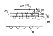
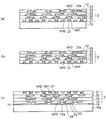
このため、図1に示すように、半導体チップ300をシリコンインターポーザ200を介して配線基板100に接続する技術が開発されている。
For this reason, as shown in FIG. 1, a technique for connecting the
配線基板100は、上面側に接続パッド120を備え、下面側に外部接続端子140を備えている。
The
シリコンインターポーザ200では、シリコン基板220にスルーホールTHが設けられており、その中に貫通電極TEが形成されている。シリコン基板220の両面側には貫通電極TEを介して相互接続された配線層240がそれぞれ形成されている。
In the
また、シリコン基板の両面側には、配線層240の上に開口部が設けられた絶縁層260がそれぞれ形成されている。
そして、シリコンインターポーザ200の下面側の配線層240が接続端子280を介して配線基板100の接続パッド120に接続されている。さらに、半導体チップ300のバンプ電極320がシリコンインターポーザ200の上面側の配線層240に接続されている。
The
このようにして、半導体チップ300の狭小ピッチのバンプ電極320が微細配線を備えたシリコンインターポーザ200に接続され、シリコンインターポーザ200から配線基板100にピッチ変換される。
In this manner, the narrow
シリコンインターポーザ200を製造する際には、シリコン基板220にドライエッチングなどでスルーホールTHを形成し、スルーホールTH内に電解めっきで貫通電極TEを形成し、両面側に微細な配線層240を形成する必要がある。
When manufacturing the
このような方法は、技術的にハードルが高く、製造できるメーカーは限られている。また、高価な製造装置の導入や煩雑な製造プロセスの遂行が必要になるため、製造コストが高くなってしまう問題がある。 Such a method is technically difficult and the number of manufacturers that can be manufactured is limited. Moreover, since it is necessary to introduce an expensive manufacturing apparatus and perform a complicated manufacturing process, there is a problem that the manufacturing cost increases.
以下に説明する実施形態では、前述した不具合を解消することができる。 In the embodiment described below, the above-described problems can be solved.
(実施形態)
図2〜図12は実施形態の配線基板の製造方法を示す断面図、図13は実施形態の配線基板を示す断面図である。以下、配線基板の製造方法を説明しながら、配線基板の構造を説明する。
(Embodiment)
2 to 12 are cross-sectional views showing a method for manufacturing a wiring board according to the embodiment, and FIG. 13 is a cross-sectional view showing the wiring board according to the embodiment. Hereinafter, the structure of the wiring board will be described while explaining the manufacturing method of the wiring board.
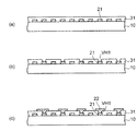
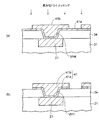
実施形態の配線基板の製造方法では、図2(a)に示すように、まず、仮基板として第1金属板10を用意する。第1金属板10の一例としては、厚みが1mm〜10mmの銅板又は銅箔が使用される。
In the wiring board manufacturing method of the embodiment, as shown in FIG. 2A, first, a
次いで、図2(b)に示すように、第1金属板10の上に、開口部11aが設けられためっきレジスト11を形成する。めっきレジスト11は、ドライフィルムレジストを第1金属板10の上に貼付し、フォトリソグラフィによって露光、現像することにより形成される。
Next, as shown in FIG. 2B, a plating resist 11 having an opening 11 a is formed on the
続いて、図2(c)に示すように、第1金属板10をめっき給電経路に利用する電解めっきにより、めっきレジスト11の開口部11aに金属めっきを施して第1配線層21を形成する。
2C, the
その後に、図2(d)に示すように、めっきレジスト11が除去される。図2(d)には、第1配線層21として、接続パッドが描かれている。第1配線層21は、島状に配置された接続パッドであってもよいし、あるいは、引き出し配線の一端に接続パッドが繋がって配置されていてもよい。
Thereafter, as shown in FIG. 2D, the
図2(d)の部分断面図に示すように、第1配線層21は積層膜で形成され、下から順に、厚みが0.5μmの金(Au)層21a/厚みが1μmのニッケル(Ni)層21b/厚みが10μmの銅(Cu)層21cから形成される。
As shown in the partial cross-sectional view of FIG. 2D, the
第1配線層21の最下層は、第1金属板10をウェットエッチングによって除去する際にストッパとなる金属から形成される。上記した例では、第1金属板10を銅から形成し、第1配線層21の最下層として金層21aを形成しているが、他の金属の組み合わせを採用してもよい。
The lowermost layer of the
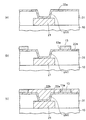
次いで、図3(a)に示すように、エポキシ樹脂又はポリイミド樹脂などの未硬化の樹脂フィルムを第1金属板10及び第1配線層21の上に貼付し、熱プレスすることにより、第1層間絶縁層31を形成する。第1層間絶縁層31の厚みは、20μm〜40μmである。第1層間絶縁層31は、ガラスクロスを含む樹脂から形成してもよい。
Next, as shown in FIG. 3A, an uncured resin film such as an epoxy resin or a polyimide resin is applied on the
続いて、図3(b)に示すように、第1層間絶縁層31をレーザで加工することにより、第1配線層21に到達する第1ビアホールVH1を形成する。レーザとしては、CO2レーザ、UV―YAGレーザ、又はエキシマレーザなどが使用される。第1ビアホールVH1の直径は、20μm〜60μmである。
Subsequently, as shown in FIG. 3B, the first via hole VH <b> 1 reaching the
第1ビアホールVH1は、第1層間絶縁層31の上面から厚み方向に向けて直径が小さくなるテーパー形状で形成される。
The first via hole VH1 is formed in a tapered shape whose diameter decreases from the upper surface of the first
その後に、図3(c)に示すように、第1ビアホールVH1内のビア導体を介して第1配線層21に接続される第2配線層22を形成する。第2配線層22は、セミアアディティブ法により形成される。
Thereafter, as shown in FIG. 3C, a
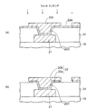
詳しく説明すると、図4(a)に示すように、まず、第1ビアホールVH1内及び第1層間絶縁層31の上に無電解めっきにより、厚みが1μm程度の銅などからなるシード層22aを形成する。
More specifically, as shown in FIG. 4A, first, a
さらに、図4(b)に示すように、シード層22aの上に、第1ビアホールVH1を含む領域に開口部13aが設けられためっきレジスト13を形成する。
Further, as shown in FIG. 4B, a plating resist 13 having an
次いで、図4(c)に示すように、シード層22aをめっき給電経路に利用する電解めっきにより、第1ビアホールVH1内からめっきレジスト13の開口部13aに銅などからなる金属めっき層22bを形成する。
Next, as shown in FIG. 4C, a
さらに、図5(a)に示すように、めっきレジスト13を除去して、シード層22aを露出させる。
Further, as shown in FIG. 5A, the plating resist 13 is removed to expose the
続いて、金属めっき層22bをマスクにしてシード層22aをウェットエッチングにより除去する。これにより、図5(b)に示すように、シード層22a及び金属めっき層22bから第2配線層22が形成される。
Subsequently, the
このとき、無電解めっきで形成されたシード層22aは電解めっきで形成された金属めっき層22bよりエッチレートがかなり高い。このため、シード層22aは金属めっき層22bの側面から内側に食い込むアンダーカット形状となってエッチングされる。また、ウェットエッチングは等方エッチングとなるため、金属めっき層22bの幅が細った状態で第2配線層22が形成される。
At this time, the
次いで、図6(a)に示すように、前述した図3(a)の第1層間絶縁層31の形成方法と同様な方法により、第1層間絶縁層31及び第2配線層22の上に第2層間絶縁層32を形成する。さらに、前述の図3(b)と同様に、第2層間絶縁層32に、第2配線層22に到達する第2ビアホールVH2を形成する。
Next, as shown in FIG. 6A, the first
続いて、図6(b)に示すように、図4(a)〜図5(b)と同様な方法により、第2ビアホールVH2内のビア導体を介して第2配線層22に接続される第3配線層23を第2層間絶縁層32の上に形成する。
Subsequently, as shown in FIG. 6 (b), it is connected to the
さらに、図6(c)に示すように、前述した図3(a)の第1層間絶縁層31の形成方法と同様な方法により、第2層間絶縁層32及び第3配線層23の上に第3層間絶縁層33を形成する。さらに、前述の図3(b)と同様に、第3層間絶縁層33に、第3配線層23に到達する第3ビアホールVH3を形成する。
Further, as shown in FIG. 6C, on the second
さらに、図6(d)に示すように、図4(a)〜図5(b)と同様な方法により、第3ビアホールVH3内のビア導体を介して第3配線層23に接続される第4配線層24を第3層間絶縁層33の上に形成する。第2〜第4配線層22,23、24の厚みは、例えば、15μm程度に設定される。また、第1〜第4配線層21〜24のライン(配線幅):スペース(配線間隔)は、例えば、10μm:10μm〜50μm:50μmの範囲から選択される。
Further, as shown in FIG. 6D, the second connection to the
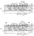
その後に、図7(a)に示すように、第3層間絶縁層33の上に、第4配線層24の接続部上に開口部12aが設けられたソルダレジスト12を保護絶縁層として形成する。
Thereafter, as shown in FIG. 7A, the solder resist 12 having the
以上により、第1金属板10の上に、第1〜第4配線層21〜24を含むベース配線基板2が形成される。
As described above, the
続いて、図7(b)に示すように、第1金属板10をウェットエッチングにより除去する。ウェットエッチングのエッチャントとしては、アンモニウム系のアルカリ水溶液が使用される。
Subsequently, as shown in FIG. 7B, the
このとき、第1配線層21の最下の金層21a(図2(d))及び第1層間絶縁層31が露出し、それらがウェットエッチングのストッパと機能して、第1配線層21のニッケル層21b及び銅層21c(図2(d))の腐食が防止される。
At this time, the
以上により、図7(a)の構造体から第1金属板10が除去されて、ベース配線基板2が得られる。ベース配線基板2は、コア基板を有さないコアレス基板として製造される。ベース配線基板2の第1配線層21の下面と第1層間絶縁層31の下面は面一になって露出する。
Thus, the
次いで、図7(c)に示すように、銅板などの第2金属板10aを用意する。そして、図7(b)のベース配線基板2を上下反転させ、第2金属板10aの上にエポキシ系の接着剤14を介してベース配線基板2を配置する。このとき、ベース配線基板2の外周部のみに接着剤14が配置されるようにする。
Next, as shown in FIG. 7C, a
さらに、その積層体を真空状態で熱プレスすることにより、接着剤14を硬化させて両者を部分的に接着させる。 Furthermore, the laminated body is hot-pressed in a vacuum state to cure the adhesive 14 and partially bond them together.
これにより、第2金属板10aの周縁部がベース配線基板2に接着され、第2金属板10aの中央部はベース配線基板2の上に単に配置された状態となる。
As a result, the peripheral edge portion of the
ベース配線基板2の上面には、第1配線層21の金属21a(図2(d))が露出した状態となる。ベース配線基板2の第1配線層21の上面と第1層間絶縁層31の上面は面一となっている。
On the upper surface of the
本実施形態では、予備的事項で説明したシリコンインターポーザ200を使用する代わりに、ベース配線基板2の上にシリコンインターポーザ200と同様な微細配線を有する再配線部を直接形成する。
In this embodiment, instead of using the
まず、図8(a)に示すように、ベース配線基板2の平坦な上面に、感光性を有する液状の樹脂層34aを塗布する。さらに、フォトリソグラフィに基づいて、フォトマスク(不図示)を介して露光した後に、現像を行い、ベーク処理をして硬化させる。
First, as shown in FIG. 8A, a photosensitive
これにより、図8(b)に示すように、第1配線層21に到達する第4ビアホールVH4が設けられた第4層間絶縁層34がベース配線基板2の上面に形成される。
Thereby, as shown in FIG. 8B, a fourth
ベース配線基板2の上に微細な再配線部を形成するため、第4層間絶縁層34の厚みは、ベース配線基板2の第1〜第3層間絶縁層31〜33の厚みよりも薄く設定される。
In order to form a fine rewiring portion on the
例えば、第4層間絶縁層34の厚みは2μm〜10μm、好適には5μm程度であり、第4ビアホールVH4の直径は10μm〜20μmである。
For example, the thickness of the fourth
ベース配線基板2の上面は平坦であり、また第4層間絶縁層34の厚みが薄いことから、フォトリソグラフィの焦点深度を十分に確保できるため、微細な第4ビアホールVH4をベース配線基板2内で均一に精度よく形成することができる。
Since the upper surface of the
第4層間絶縁層34の第4ビアホールVH4は、製造途中で上下反転したベース配線基板2の上に配置され、上面から厚み方向に向けて直径が小さくなるテーパー形状で形成される。このため、第4ビアホールVH4はベース配線基板2の第1ビアホールVH1と逆のテーパー形状となって配置される。
The fourth via hole VH4 of the fourth
次いで、図8(c)に示すように、第4ビアホールVH4内のビア導体を介して第1配線層21に接続される第1再配線層41を第4層間絶縁層34の上に形成する。第1再配線層41は、セミアディティブ法によって形成される。
Next, as shown in FIG. 8C, a
詳しく説明すると、図9(a)に示すように、まず、第4ビアホールVH4内及び第4層間絶縁層34の上にシード層41aをスパッタ法により形成する。図9(a)の部分断面図に示すように、シード層41aは、下から順に、厚みが20nmのチタン(Ti)層41x/厚みが300nmの銅(Cu)層41yから形成される。
More specifically, as shown in FIG. 9A, first, a
チタン層41xは、第4層間絶縁層34(樹脂)と銅層41yとを密着させる密着層として機能する。
The
シード層41aをスパッタ法で形成することにより、無電解めっきを採用する場合よりも成膜の信頼性が高いため厚みを薄く設定できる。このため、シード層41aのエッチングが容易になり、再配線層の微細化に対応することができる。
By forming the
その後に、図9(b)に示すように、シード層41aの上に、第4ビアホールVH4を含む領域に開口部15aが設けられためっきレジスト15を形成する。
Thereafter, as shown in FIG. 9B, a plating resist 15 having an
このとき、ベース配線基板2の上面は平坦であることから、フォトリソグラフィの焦点深度を十分に確保できるため、めっきレジスト15の開口部15aをベース配線基板2内で均一に精度よく形成することができる。
At this time, since the upper surface of the
次いで、図9(c)に示すように、シード層41aをめっき給電経路に利用する電解めっきにより、第4ビアホールVH4内からめっきレジスト15の開口部15aに銅などからなる金属めっき層41bを形成する。金属めっき層41bの厚みは、例えば、1μm〜4μmに設定される。
Next, as shown in FIG. 9C, a
さらに、図10(a)に示すように、めっきレジスト15を除去して、シード層41aを露出させる。続いて、塩素系のガスを使用する異方性ドライエッチングにより、金属めっき層41bをマスクにしてシード層41aをエッチングして除去する。
Further, as shown in FIG. 10A, the plating resist 15 is removed to expose the
これにより、図10(b)に示すように、シード層41a及び金属めっき層41bから第1再配線層41が形成される。第1再配線層41のトータルの厚みは、5μm程度以下、好適には、2μm〜3μmである。
Thereby, as shown in FIG. 10B, the
異方性ドライエッチングは、RIE(Reactive Ion Etching)装置、又はICP(Inductively Coupled Plasma)装置などのドライエッチング装置によって行われる。 The anisotropic dry etching is performed by a dry etching apparatus such as an RIE (Reactive Ion Etching) apparatus or an ICP (Inductively Coupled Plasma) apparatus.
異方性ドライエッチングを採用することにより、金属めっき層41の細りを微小に抑えることができると共に、シード層41aが金属めっき層41bの側面から内側にサイドエッチングすることがない。しかも、スパッタ法を採用することにより、シード層41aを薄膜化できるため、微細化に有利になる。
By employing anisotropic dry etching, the
このため、ライン:スペースが1μm:1μm〜5μm:5μmの微細な再配線層41を設計スペック内で歩留りよく形成することができる。
Therefore, a
シード層41aが銅から形成される場合は、ドライエッチング時に発生する銅の塩化物は揮発性が低いため、エッチング装置のステージの温度を100℃〜200℃に設定して高温雰囲気でエッチングすることが好ましい。
When the
前述した図4(a)〜図5(b)で説明したように、シード層をウェットエッチングで除去する場合は、第1再配線層41の細りやパターン飛びが発生しやすく、微細な第1再配線層41を歩留りよく形成することは困難である。
As described above with reference to FIGS. 4A to 5B, when the seed layer is removed by wet etching, the
このようにして、第1再配線層41の幅をベース配線基板2の第1〜第4配線層21〜24の幅よりも細く設定することができる。
In this way, the width of the
また、第1再配線層41を形成する際にシード層41aを異方性ドライエッチングにより除去するため、シード層41aの幅は金属めっき層41bの幅と同一又はそれより広くなる。図10(b)の例では、シード層41aの幅が金属めっき層41bの幅と同一になっている。
Further, since the
これ以外に、ドライエッチングの条件によっては、シード層41aの側面が金属めっき層41bの下端から下側になるにつれて広がる裾引き形状になって、シード層41aの幅が金属めっき層41bの幅より広くなる場合もある。
In addition to this, depending on the dry etching conditions, the side surface of the
次いで、図11(a)に示すように、前述した図8(a)及び(b)と同様な方法により、第1再配線層41の上に第5ビアホールVH5が設けられた第5層間絶縁層35を第4層間絶縁層34の上に形成する。
Next, as shown in FIG. 11A, a fifth interlayer insulation in which a fifth via hole VH5 is provided on the
続いて、図11(b)に示すように、図9(a)〜図10(b)と同様な方法により、第5ビアホールVH5内のビア導体を介して第1再配線層41に接続される第2再配線層42を第5層間絶縁層35の上に形成する。
Subsequently, as shown in FIG. 11B, the
さらに、図11(c)に示すように、前述した図8(a)及び(b)と同様な方法により、第2再配線層42上に第6ビアホールVH6が設けられた第6層間絶縁層36を第5層間絶縁層35の上に形成する。
Further, as shown in FIG. 11C, a sixth interlayer insulating layer in which a sixth via hole VH6 is provided on the
次いで、図12(a)に示すように、図9(a)〜図10(b)と同様な方法により、第6ビアホールVH6に第2再配線層42に接続される第3再配線層43を形成する。第3再配線層43は、第6ビアホールVH6から上側に突出するポスト電極として形成される。第3再配線層43は、第6層間絶縁層36の上面から10μm程度の高さで形成される。
Next, as shown in FIG. 12A, the
以上により、ベース配線基板2の上に第1〜第3再配線層41,42、43及び第4〜第6層間絶縁層34,35、36を含む再配線部3が形成される。
As described above, the
その後に、図12(b)に示すように、図12(a)の構造体の接着剤14が配置された領域よりも内側の位置で、第6層間絶縁層36の上面から第2金属板10aの下面まで切断する。このとき、図12(b)の構造体では、接着剤14の位置よりも内側領域では、第2金属板10aとベース配線基板2とは接着されていないため、両者を容易に分離することができる。
Thereafter, as shown in FIG. 12B, the second metal plate is formed from the upper surface of the sixth
これにより、図13に示すように、本実施形態の配線基板1が得られる。
Thereby, as shown in FIG. 13, the
以上のように、本実施形態の配線基板の製造方法では、第1金属板10の上にベース配線基板2を形成した後に、第1金属板10を除去する。次いで、ベース配線基板2の平坦な露出面の上に、第1配線層21に接続される再配線部3を形成する。
As described above, in the method for manufacturing a wiring board according to the present embodiment, after the
再配線部3では、感光性を有する樹脂材料をフォトリソグラフィでパターン化することにより、微細なビアホールを備えて厚みが5μm程度の薄膜の第1〜第3層間絶縁層35,36,37を形成することができる。
In the
また、第1再配線層41などをセミアディティブ法で形成する際に、シード層41aをスパッタ法により薄膜で形成し、金属めっき層41bをマスクにしてシード層41aを除去するときに異方性ドライエッチングを採用している。
Further, when the
このようなドライプロセスを使用することにより、シリコンインターポーザと同等な微細な第1〜第3再配線層41〜43を形成することができる。 By using such a dry process, the fine first to third redistribution layers 41 to 43 equivalent to the silicon interposer can be formed.
なお、前述した形態では、第1〜第3再配線層41〜43をセミアディティブ法で形成している。他の形態として、スパッタ法により、チタン層/銅層などの金属層を一面に形成し、フォトリソグラフィでレジストパターンを形成した後に、異方性ドライエッチングで金属層をエッチングすることにより、再配線層を形成してもよい。 In the above-described embodiment, the first to third rewiring layers 41 to 43 are formed by a semi-additive method. As another form, a metal layer such as a titanium layer / copper layer is formed on one surface by sputtering, a resist pattern is formed by photolithography, and then the metal layer is etched by anisotropic dry etching, thereby rewiring. A layer may be formed.
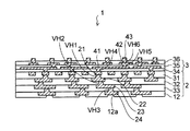
図13に示すように、本実施形態の配線基板1は、ベース配線基板2とその上に形成された再配線部3とを備えている。
As shown in FIG. 13, the
本実施形態の配線基板1は前述した製造方法で製造されるため、ベース配線基板2では、第1配線層21の横方向及び下側に第1層間絶縁層31が配置されている。第1配線層21の下面及び側面が第1層間絶縁層31内に埋め込まれており、第1配線層21の上面が第1層間絶縁層31から露出している。また、第1配線層21の上面及び第1層間絶縁層31の上面は面一となっている。
Since the
第1層間絶縁層31は第1配線層21の下に第1ビアホールVH1を備えている。第1ビアホールVH1は、第1層間絶縁層31の下面から第1配線層21の下面に到達して形成されている。
The first
第1層間絶縁層31の下には、第1ビアホールVH1内のビア導体を介して第1配線層21に接続される第2配線層22が形成されている。
A
また同様に、第2配線層22の横方向及び下側に第2層間絶縁層32が形成されている。第2層間絶縁層32は、第2配線層22の下に第2ビアホールVH2を備えている。第2層間絶縁層32の下には、第2ビアホールVH2内のビア導体を介して第2配線層22に接続される第3配線層23が形成されている。
Similarly, a second
また同様に、第3配線層23の横方向及び下に第3層間絶縁層33が形成されている。第3層間絶縁層33は第3配線層23の下に第3ビアホールVH3が形成されている。第3層間絶縁層33の下には、第3ビアホールVH3内のビア導体を介して第3配線層23に接続される第4配線層24が形成されている。
Similarly, a third
さらに、第3層間絶縁層33の下には、第4配線層24の接続部上に開口部12aが設けられたソルダレジスト12が保護絶縁層として形成されている。
Further, below the third
第2〜第4配線層22〜24は、第1、第2、第3層間絶縁層31〜33の下面から下側にそれぞれ突き出た状態で形成されている。
The second to fourth wiring layers 22 to 24 are formed so as to protrude downward from the lower surfaces of the first, second, and third
また、ベース配線基板2の第1〜第3ビアホールVH1〜VH3は、第1、第2、第3層間絶縁層31,32、33の下面からその厚み方向に向けて直径が小さくなるテーパー形状で形成されている。
The first to third via holes VH1 to VH3 of the
また、ベース配線基板2の第1層間絶縁層31の上には再配線部3の第4層間絶縁層34が形成されている。第4層間絶縁層34は、ベース配線基板2の第1配線層21の上に第4ビアホールVH4を備えている。
In addition, a fourth
第4層間絶縁層34の上には、第4ビアホールVH4内のビア導体を介して第1配線層21に接続される第1再配線層41が形成されている。第4層間絶縁層34の上には、第1再配線層41の上に第5ビアホールVH5を備えた第5層間絶縁層35が形成されている。
On the fourth
第5層間絶縁層35の上には、第5ビアホールVH5内のビア導体を介して第1再配線層41に接続される第2再配線層42が形成されている。第5層間絶縁層35の上には、第2再配線層42の上に第6ビアホールVH6を備えた第6層間絶縁層36が形成されている。
On the fifth
第6ビアホールVH6内には、第2再配線層42に接続されて、第6層間絶縁層36から上側に突出する第3再配線層43がポスト電極として形成されている。
In the sixth via hole VH6, a
製造途中で上下反転したベース配線基板2の上に再配線部3が形成されるため、再配線部3の第4〜第6ビアホールV4〜V6は、ベース配線基板2の第1〜第3ビアホールVH1〜VH3と逆のテーパー形状となって配置されている。
Since the
第1〜第3再配線層41〜43、及び第4〜第6層間絶縁層34〜36から再配線部3が形成されている。
A
本実施形態の配線基板1では、コアレスタイプのベース配線基板2の第1配線層21が露出する平坦面の上に再配線部3が直接形成された構造を有する。再配線部3の第1〜第3再配線層41〜43の各幅は、ベース配線基板2の第1〜第4配線層21〜24の各幅より細く設定されている。
The
好適には、再配線部3の各再配線層41〜43はライン:スペースが1μm:1μm〜5μm:5μmの微細配線であり、シリコンインターポーザの役割を果たすことができる。また、再配線部3の第4〜第6層間絶縁層34〜36の各厚みは、ベース配線基板2の第1〜第3層間絶縁層31〜33の各厚みより薄く設定されている。
Preferably, each of the rewiring layers 41 to 43 of the
このように、本実施形態の配線基板1は、ベース配線基板2とシリコンインターポーザの役割を果たす再配線部3とが一体的に形成されている。
Thus, in the
このため、技術的にハードルが高く、製造コストが高いシリコンインターポーザを使用する必要がない。 For this reason, it is not necessary to use a silicon interposer that has high technical hurdles and high manufacturing costs.
また、シリコンインターポーザを使用する場合は、シリコン基板の厚みだけで100μm程度以上であり、その両面に多層配線層を形成することを考慮すると、薄型化する際に限界がある。 When using a silicon interposer, the thickness of the silicon substrate alone is about 100 μm or more, and considering the formation of multilayer wiring layers on both sides thereof, there is a limit in reducing the thickness.
しかし、本実施形態の配線基板1では、再配線部3にはシリコン基板を使用せず、層間絶縁層の厚みを5μm程度に、再配線層の厚みを2μm〜3μm程度に薄く設定できるため、シリコンインターポーザを使用する場合よりも薄型化を図ることができる。
However, in the
図14には、図13の配線基板1の上に半導体チップが搭載された半導体装置の一例が示されている。図14に示すように、図13の配線基板1の再配線部3の第3再配線層43に半導体チップ50のバンプ電極52がフリップチップ接続される。さらに、半導体チップ50と配線基板1の再配線部3との隙間にアンダーフィル樹脂54が充填される。
FIG. 14 shows an example of a semiconductor device in which a semiconductor chip is mounted on the
また、配線基板1のベース配線基板2の下側の第4配線層24にはんだボールを搭載するなどして外部接続端子56を形成する。
Further, the
このようにして、半導体チップ50の狭小ピッチのバンプ電極52が微細配線を備えた再配線部3に接続され、再配線部3からベース配線基板2にピッチ変換される。
In this way, the narrow
シリコンインターポーザを使用する場合は、ベース配線基板の上にシリコンインターポーザを実装し、さらにシリコンインターザの上に半導体チップを実装するする一連の工程が必要である。しかし、本実施形態では、配線基板1の再配線部3に半導体チップ50を実装するだけでよく、実装工程を簡略化することができる。
When the silicon interposer is used, a series of steps of mounting the silicon interposer on the base wiring substrate and further mounting the semiconductor chip on the silicon interposer is necessary. However, in this embodiment, it is only necessary to mount the
配線基板1に搭載する電子部品として半導体チップ50を例示するが、各種の電子部品の実装基板として使用することができる。
Although the
1…配線基板、2…ベース配線基板、3…再配線部、10…第1金属板、10a…第2金属板、11,13,15…めっきレジスト、開口部…11a,12a,13a,15a、12…ソルダレジスト、14…接着剤、21…第1配線層、22…第2配線層、22a,41a…シード層、22b,41b…金属めっき層、23…第3配線層、24…第4配線層、31…第1層間絶縁層、32…第2層間絶縁層、33…第3層間絶縁層、34…第4層間絶縁層、35…第5層間絶縁層、36…第6層間絶縁層、41…第1再配線層、42…第2再配線層、43…第3再配線層、50…半導体チップ、52…バンプ電極、54…アンダーフィル樹脂、56…外部接続端子、VH1,VH2,VH3,VH4,VH5,VH6…ビアホール。
DESCRIPTION OF
Claims (10)
前記第1配線層が埋め込まれ、前記第1配線層の下に第1ビアホールが形成された第1絶縁層と、
前記第1絶縁層の下に形成され、前記第1ビアホール内のビア導体を介して前記第1配線層に接続された第2配線層と
を備えたベース配線基板と、
前記ベース配線基板の上に形成され、前記第1配線層の上に第2ビアホールが形成された第2絶縁層と、
前記第2絶縁層の上に形成され、前記第2ビアホール内のビア導体を介して前記第1配線層に接続された再配線層とを備えた再配線部と
を有し、
前記再配線層はシード層及びその上の金属めっき層から形成され、前記シード層の幅は前記金属めっき層の幅と同一又はそれより広いことを特徴とする配線基板。 A first wiring layer;
A first insulating layer in which the first wiring layer is embedded and a first via hole is formed under the first wiring layer;
A base wiring board comprising: a second wiring layer formed under the first insulating layer and connected to the first wiring layer via a via conductor in the first via hole;
A second insulating layer formed on the base wiring substrate and having a second via hole formed on the first wiring layer;
A redistribution portion including a redistribution layer formed on the second insulating layer and connected to the first wiring layer via a via conductor in the second via hole,
The rewiring layer is formed of a seed layer and a metal plating layer thereon, and the width of the seed layer is the same as or wider than the width of the metal plating layer.
前記金属板の上に、前記第1配線層の上に第1ビアホールが設けられた第1絶縁層を形成する工程と、
前記第1ビアホール内のビア導体を介して前記第1配線層に接続される第2配線層を前記第1絶縁層の上に形成する工程と、
前記金属板を除去する工程と、
前記第1絶縁層の上に、前記第1配線層の上に第2ビアホールが設けられた第2絶縁層を形成する工程と、
前記第2ビアホール内及び前記第2絶縁層の上にシード層を形成する工程と、
前記第2ビアホールを含む領域に開口部が設けられためっきレジストを形成する工程と、
電解めっきにより、前記第2ビアホール及び前記めっきレジストの開口部に金属めっき層を形成する工程と、
前記めっきレジストを除去する工程と、
異方性ドライエッチングにより、前記金属めっき層をマスクにして前記シード層を除去することにより、再配線層を形成する工程とを有することを特徴とする配線基板の製造方法。 Forming a first wiring layer on the metal plate;
Forming a first insulating layer provided with a first via hole on the first wiring layer on the metal plate;
Forming a second wiring layer on the first insulating layer connected to the first wiring layer via a via conductor in the first via hole;
Removing the metal plate;
Forming a second insulating layer provided with a second via hole on the first wiring layer on the first insulating layer;
Forming a seed layer in the second via hole and on the second insulating layer;
Forming a plating resist having an opening in a region including the second via hole;
Forming a metal plating layer on the opening of the second via hole and the plating resist by electrolytic plating;
Removing the plating resist;
And a step of forming a rewiring layer by removing the seed layer by anisotropic dry etching using the metal plating layer as a mask.
前記第1配線層の下面と前記第1絶縁層の下面とが面一になって露出することを特徴とする請求項6に記載の配線基板の製造方法。 In the step of removing the metal plate,
The method of manufacturing a wiring board according to claim 6, wherein the lower surface of the first wiring layer and the lower surface of the first insulating layer are exposed in a flush manner.
Priority Applications (2)
| Application Number | Priority Date | Filing Date | Title |
|---|---|---|---|
| JP2013025210A JP2014154800A (en) | 2013-02-13 | 2013-02-13 | Wiring board and manufacturing method thereof |
| US14/141,765 US9455219B2 (en) | 2013-02-13 | 2013-12-27 | Wiring substrate and method of manufacturing the same |
Applications Claiming Priority (1)
| Application Number | Priority Date | Filing Date | Title |
|---|---|---|---|
| JP2013025210A JP2014154800A (en) | 2013-02-13 | 2013-02-13 | Wiring board and manufacturing method thereof |
Publications (2)
| Publication Number | Publication Date |
|---|---|
| JP2014154800A true JP2014154800A (en) | 2014-08-25 |
| JP2014154800A5 JP2014154800A5 (en) | 2016-01-28 |
Family
ID=51296947
Family Applications (1)
| Application Number | Title | Priority Date | Filing Date |
|---|---|---|---|
| JP2013025210A Pending JP2014154800A (en) | 2013-02-13 | 2013-02-13 | Wiring board and manufacturing method thereof |
Country Status (2)
| Country | Link |
|---|---|
| US (1) | US9455219B2 (en) |
| JP (1) | JP2014154800A (en) |
Cited By (13)
| Publication number | Priority date | Publication date | Assignee | Title |
|---|---|---|---|---|
| JP2016127248A (en) * | 2015-01-08 | 2016-07-11 | 日本特殊陶業株式会社 | Multilayer wiring board |
| JP2017050310A (en) * | 2015-08-31 | 2017-03-09 | 新光電気工業株式会社 | Electronic component device and manufacturing method thereof |
| WO2017043375A1 (en) * | 2015-09-08 | 2017-03-16 | 東レ株式会社 | Photosensitive resin composition, photosensitive sheet, semiconductor device, and method for manufacturing semiconductor device |
| WO2017073481A1 (en) * | 2015-10-28 | 2017-05-04 | 東レ株式会社 | Positive photosensitive resin composition, photosensitive sheet, cured film, interlayer insulating film, semiconductor protective film, method for manufacturing semiconductor device, semiconductor electronic component and semiconductor device |
| WO2017170032A1 (en) * | 2016-03-28 | 2017-10-05 | 東レ株式会社 | Photosensitive film |
| KR20190011125A (en) * | 2017-07-24 | 2019-02-01 | 삼성전자주식회사 | Semiconductor package and method for manufacturing the same |
| CN109561569A (en) * | 2017-09-27 | 2019-04-02 | 揖斐电株式会社 | Printed wiring board |
| JP2019125709A (en) * | 2018-01-17 | 2019-07-25 | 新光電気工業株式会社 | Wiring board, manufacturing method thereof, and electronic component device |
| KR20190093191A (en) * | 2016-12-30 | 2019-08-08 | 인텔 코포레이션 | Package board with high density interconnect layer with filler and via connections for fan out scaling |
| JP2020521347A (en) * | 2017-04-21 | 2020-07-16 | フラウンホーファー−ゲゼルシャフト・ツール・フェルデルング・デル・アンゲヴァンテン・フォルシュング・アインゲトラーゲネル・フェライン | MEMS transducer interacting with fluid volumetric flow rate and method of making same |
| US10804191B2 (en) | 2017-10-11 | 2020-10-13 | Ibiden Co., Ltd. | Printed wiring board |
| US11088081B2 (en) | 2018-10-02 | 2021-08-10 | Samsung Electronics Co., Ltd. | Semiconductor package having a connection structure with tapering connection via layers |
| US11177205B2 (en) | 2018-12-18 | 2021-11-16 | Samsung Electronics Co., Ltd. | Semiconductor package having multi-level and multi-directional shape narrowing vias |
Families Citing this family (7)
| Publication number | Priority date | Publication date | Assignee | Title |
|---|---|---|---|---|
| US9252110B2 (en) | 2014-01-17 | 2016-02-02 | Taiwan Semiconductor Manufacturing Company, Ltd. | Interconnect structure and method of forming same |
| JP6133227B2 (en) * | 2014-03-27 | 2017-05-24 | 新光電気工業株式会社 | Wiring board and manufacturing method thereof |
| TWI566305B (en) * | 2014-10-29 | 2017-01-11 | 巨擘科技股份有限公司 | Method for manufacturing three-dimensional integrated circuit |
| US10504874B2 (en) * | 2016-08-01 | 2019-12-10 | Taiwan Semiconductor Manufacturing Company Limited | Structures and methods for providing electrical isolation in semiconductor devices |
| CN112289688A (en) * | 2019-07-22 | 2021-01-29 | 中芯长电半导体(江阴)有限公司 | Preparation method of rewiring layer |
| KR20210026546A (en) | 2019-08-30 | 2021-03-10 | 삼성전자주식회사 | Method for manufacturing semiconductor package |
| KR20220046134A (en) | 2020-10-07 | 2022-04-14 | 삼성전자주식회사 | Semiconductor package |
Citations (5)
| Publication number | Priority date | Publication date | Assignee | Title |
|---|---|---|---|---|
| JP2007234889A (en) * | 2006-03-01 | 2007-09-13 | Shinko Electric Ind Co Ltd | Method of forming wiring |
| WO2010010910A1 (en) * | 2008-07-23 | 2010-01-28 | 日本電気株式会社 | Coreless wiring substrate, semiconductor device, and methods for manufacturing same |
| JP2010157690A (en) * | 2008-12-29 | 2010-07-15 | Ibiden Co Ltd | Board for mounting electronic component thereon, and method of manufacturing the same |
| JP2011014847A (en) * | 2009-07-06 | 2011-01-20 | Shinko Electric Ind Co Ltd | Multilayer wiring board |
| WO2011089936A1 (en) * | 2010-01-22 | 2011-07-28 | 日本電気株式会社 | Substrate with built-in functional element, and wiring substrate |
Family Cites Families (11)
| Publication number | Priority date | Publication date | Assignee | Title |
|---|---|---|---|---|
| JP3961092B2 (en) * | 1997-06-03 | 2007-08-15 | 株式会社東芝 | Composite wiring board, flexible substrate, semiconductor device, and method of manufacturing composite wiring board |
| JPH11126978A (en) | 1997-10-24 | 1999-05-11 | Kyocera Corp | Multilayered wiring board |
| KR100385042B1 (en) * | 1998-12-03 | 2003-06-18 | 인터내셔널 비지네스 머신즈 코포레이션 | Method for forming electromigration-resistant structures by doping |
| US6375693B1 (en) * | 1999-05-07 | 2002-04-23 | International Business Machines Corporation | Chemical-mechanical planarization of barriers or liners for copper metallurgy |
| US6573822B2 (en) * | 2001-06-18 | 2003-06-03 | Intel Corporation | Tunable inductor using microelectromechanical switches |
| US6812576B1 (en) * | 2002-05-14 | 2004-11-02 | Applied Micro Circuits Corporation | Fanned out interconnect via structure for electronic package substrates |
| US6818469B2 (en) * | 2002-05-27 | 2004-11-16 | Nec Corporation | Thin film capacitor, method for manufacturing the same and printed circuit board incorporating the same |
| US7265038B2 (en) * | 2003-11-25 | 2007-09-04 | Taiwan Semiconductor Manufacturing Co., Ltd. | Method for forming a multi-layer seed layer for improved Cu ECP |
| US7834273B2 (en) * | 2005-07-07 | 2010-11-16 | Ibiden Co., Ltd. | Multilayer printed wiring board |
| JPWO2009147936A1 (en) * | 2008-06-02 | 2011-10-27 | イビデン株式会社 | Manufacturing method of multilayer printed wiring board |
| JP2012216773A (en) * | 2011-03-29 | 2012-11-08 | Shinko Electric Ind Co Ltd | Wiring board and manufacturing method thereof |
-
2013
- 2013-02-13 JP JP2013025210A patent/JP2014154800A/en active Pending
- 2013-12-27 US US14/141,765 patent/US9455219B2/en active Active
Patent Citations (5)
| Publication number | Priority date | Publication date | Assignee | Title |
|---|---|---|---|---|
| JP2007234889A (en) * | 2006-03-01 | 2007-09-13 | Shinko Electric Ind Co Ltd | Method of forming wiring |
| WO2010010910A1 (en) * | 2008-07-23 | 2010-01-28 | 日本電気株式会社 | Coreless wiring substrate, semiconductor device, and methods for manufacturing same |
| JP2010157690A (en) * | 2008-12-29 | 2010-07-15 | Ibiden Co Ltd | Board for mounting electronic component thereon, and method of manufacturing the same |
| JP2011014847A (en) * | 2009-07-06 | 2011-01-20 | Shinko Electric Ind Co Ltd | Multilayer wiring board |
| WO2011089936A1 (en) * | 2010-01-22 | 2011-07-28 | 日本電気株式会社 | Substrate with built-in functional element, and wiring substrate |
Cited By (21)
| Publication number | Priority date | Publication date | Assignee | Title |
|---|---|---|---|---|
| JP2016127248A (en) * | 2015-01-08 | 2016-07-11 | 日本特殊陶業株式会社 | Multilayer wiring board |
| JP2017050310A (en) * | 2015-08-31 | 2017-03-09 | 新光電気工業株式会社 | Electronic component device and manufacturing method thereof |
| WO2017043375A1 (en) * | 2015-09-08 | 2017-03-16 | 東レ株式会社 | Photosensitive resin composition, photosensitive sheet, semiconductor device, and method for manufacturing semiconductor device |
| WO2017073481A1 (en) * | 2015-10-28 | 2017-05-04 | 東レ株式会社 | Positive photosensitive resin composition, photosensitive sheet, cured film, interlayer insulating film, semiconductor protective film, method for manufacturing semiconductor device, semiconductor electronic component and semiconductor device |
| WO2017170032A1 (en) * | 2016-03-28 | 2017-10-05 | 東レ株式会社 | Photosensitive film |
| JPWO2017170032A1 (en) * | 2016-03-28 | 2019-02-07 | 東レ株式会社 | Photosensitive film |
| KR102596788B1 (en) * | 2016-12-30 | 2023-10-31 | 인텔 코포레이션 | Package substrate with high-density interconnection layers with pillar and via connections for fan-out scaling |
| KR20190093191A (en) * | 2016-12-30 | 2019-08-08 | 인텔 코포레이션 | Package board with high density interconnect layer with filler and via connections for fan out scaling |
| JP2020521347A (en) * | 2017-04-21 | 2020-07-16 | フラウンホーファー−ゲゼルシャフト・ツール・フェルデルング・デル・アンゲヴァンテン・フォルシュング・アインゲトラーゲネル・フェライン | MEMS transducer interacting with fluid volumetric flow rate and method of making same |
| US11554950B2 (en) | 2017-04-21 | 2023-01-17 | Fraunhofer-Gesellschaft zur Förderung der angewandten Forschung e.V. | MEMS transducer for interacting with a volume flow of a fluid, and method of producing same |
| KR20190011125A (en) * | 2017-07-24 | 2019-02-01 | 삼성전자주식회사 | Semiconductor package and method for manufacturing the same |
| KR102412613B1 (en) * | 2017-07-24 | 2022-06-23 | 삼성전자주식회사 | Semiconductor package and method for manufacturing the same |
| CN109561569A (en) * | 2017-09-27 | 2019-04-02 | 揖斐电株式会社 | Printed wiring board |
| CN109561569B (en) * | 2017-09-27 | 2023-12-29 | 揖斐电株式会社 | Printed wiring board |
| US10804191B2 (en) | 2017-10-11 | 2020-10-13 | Ibiden Co., Ltd. | Printed wiring board |
| JP7032148B2 (en) | 2018-01-17 | 2022-03-08 | 新光電気工業株式会社 | Wiring board and its manufacturing method and electronic component equipment |
| JP2019125709A (en) * | 2018-01-17 | 2019-07-25 | 新光電気工業株式会社 | Wiring board, manufacturing method thereof, and electronic component device |
| US11088081B2 (en) | 2018-10-02 | 2021-08-10 | Samsung Electronics Co., Ltd. | Semiconductor package having a connection structure with tapering connection via layers |
| US11670518B2 (en) | 2018-10-02 | 2023-06-06 | Samsung Electronics Co., Ltd. | Method of manufacturing semiconductor package having connection structure with tapering connection via layers |
| US11177205B2 (en) | 2018-12-18 | 2021-11-16 | Samsung Electronics Co., Ltd. | Semiconductor package having multi-level and multi-directional shape narrowing vias |
| US11967549B2 (en) | 2018-12-18 | 2024-04-23 | Samsung Electronics Co., Ltd. | Semiconductor package |
Also Published As
| Publication number | Publication date |
|---|---|
| US9455219B2 (en) | 2016-09-27 |
| US20140225275A1 (en) | 2014-08-14 |
Similar Documents
| Publication | Publication Date | Title |
|---|---|---|
| JP2014154800A (en) | Wiring board and manufacturing method thereof | |
| JP5395360B2 (en) | Manufacturing method of electronic component built-in substrate | |
| US8410614B2 (en) | Semiconductor device having a semiconductor element buried in an insulating layer and method of manufacturing the same | |
| JP4716819B2 (en) | Manufacturing method of interposer | |
| JP2010034403A (en) | Wiring substrate and electronic component device | |
| US20150364405A1 (en) | Wiring substrate and method of manufacturing the same | |
| US9899235B2 (en) | Fabrication method of packaging substrate | |
| US9711476B2 (en) | Wiring board and electronic component device | |
| JP2017163027A (en) | Wiring board, semiconductor device, and manufacturing method for wiring board | |
| JP2014236102A (en) | Wiring board with through electrode, manufacturing method of the same, and semiconductor device | |
| JP6418757B2 (en) | WIRING BOARD, MANUFACTURING METHOD THEREOF, AND SEMICONDUCTOR DEVICE | |
| JP6316609B2 (en) | WIRING BOARD, SEMICONDUCTOR DEVICE, WIRING BOARD MANUFACTURING METHOD, AND SEMICONDUCTOR DEVICE MANUFACTURING METHOD | |
| JP2018032657A (en) | Printed wiring board and method for manufacturing printed wiring board | |
| US10129980B2 (en) | Circuit board and electronic component device | |
| JP6092555B2 (en) | Wiring board manufacturing method | |
| US20160353576A1 (en) | Electronic component built-in substrate and electronic device | |
| JP4398683B2 (en) | Manufacturing method of multilayer wiring board | |
| TWI771534B (en) | Wiring board and manufacturing method thereof | |
| JP2011187912A (en) | Electro device-embedded printed circuit board and manufacturing method thereof | |
| KR101039774B1 (en) | Method of fabricating a metal bump for printed circuit board | |
| JP2008288607A (en) | Method for manufacturing electronic parts packaging structure | |
| KR100908986B1 (en) | Coreless Package Substrate and Manufacturing Method | |
| KR101158213B1 (en) | Printed Circuit Board with Electronic Components Embedded therein and Method for Fabricating the same | |
| JP5419583B2 (en) | Wiring board manufacturing method | |
| TWI527164B (en) | Method for forming a package substrate |
Legal Events
| Date | Code | Title | Description |
|---|---|---|---|
| A521 | Request for written amendment filed |
Free format text: JAPANESE INTERMEDIATE CODE: A523 Effective date: 20151202 |
|
| A621 | Written request for application examination |
Free format text: JAPANESE INTERMEDIATE CODE: A621 Effective date: 20151202 |
|
| A977 | Report on retrieval |
Free format text: JAPANESE INTERMEDIATE CODE: A971007 Effective date: 20160927 |
|
| A131 | Notification of reasons for refusal |
Free format text: JAPANESE INTERMEDIATE CODE: A131 Effective date: 20161011 |
|
| A02 | Decision of refusal |
Free format text: JAPANESE INTERMEDIATE CODE: A02 Effective date: 20170606 |