JP7325258B2 - エキスパンド装置 - Google Patents
エキスパンド装置 Download PDFInfo
- Publication number
- JP7325258B2 JP7325258B2 JP2019148838A JP2019148838A JP7325258B2 JP 7325258 B2 JP7325258 B2 JP 7325258B2 JP 2019148838 A JP2019148838 A JP 2019148838A JP 2019148838 A JP2019148838 A JP 2019148838A JP 7325258 B2 JP7325258 B2 JP 7325258B2
- Authority
- JP
- Japan
- Prior art keywords
- workpiece
- expanding
- unit
- frame
- hot air
- Prior art date
- Legal status (The legal status is an assumption and is not a legal conclusion. Google has not performed a legal analysis and makes no representation as to the accuracy of the status listed.)
- Active
Links
Images


Classifications
-
- H—ELECTRICITY
- H01—ELECTRIC ELEMENTS
- H01L—SEMICONDUCTOR DEVICES NOT COVERED BY CLASS H10
- H01L21/00—Processes or apparatus adapted for the manufacture or treatment of semiconductor or solid state devices or of parts thereof
- H01L21/67—Apparatus specially adapted for handling semiconductor or electric solid state devices during manufacture or treatment thereof; Apparatus specially adapted for handling wafers during manufacture or treatment of semiconductor or electric solid state devices or components ; Apparatus not specifically provided for elsewhere
- H01L21/67005—Apparatus not specifically provided for elsewhere
- H01L21/67011—Apparatus for manufacture or treatment
- H01L21/67132—Apparatus for placing on an insulating substrate, e.g. tape
-
- H—ELECTRICITY
- H01—ELECTRIC ELEMENTS
- H01L—SEMICONDUCTOR DEVICES NOT COVERED BY CLASS H10
- H01L21/00—Processes or apparatus adapted for the manufacture or treatment of semiconductor or solid state devices or of parts thereof
- H01L21/67—Apparatus specially adapted for handling semiconductor or electric solid state devices during manufacture or treatment thereof; Apparatus specially adapted for handling wafers during manufacture or treatment of semiconductor or electric solid state devices or components ; Apparatus not specifically provided for elsewhere
- H01L21/67005—Apparatus not specifically provided for elsewhere
- H01L21/67011—Apparatus for manufacture or treatment
- H01L21/67092—Apparatus for mechanical treatment
-
- H—ELECTRICITY
- H01—ELECTRIC ELEMENTS
- H01L—SEMICONDUCTOR DEVICES NOT COVERED BY CLASS H10
- H01L21/00—Processes or apparatus adapted for the manufacture or treatment of semiconductor or solid state devices or of parts thereof
- H01L21/67—Apparatus specially adapted for handling semiconductor or electric solid state devices during manufacture or treatment thereof; Apparatus specially adapted for handling wafers during manufacture or treatment of semiconductor or electric solid state devices or components ; Apparatus not specifically provided for elsewhere
- H01L21/67005—Apparatus not specifically provided for elsewhere
- H01L21/67011—Apparatus for manufacture or treatment
- H01L21/67098—Apparatus for thermal treatment
- H01L21/67109—Apparatus for thermal treatment mainly by convection
-
- H—ELECTRICITY
- H01—ELECTRIC ELEMENTS
- H01L—SEMICONDUCTOR DEVICES NOT COVERED BY CLASS H10
- H01L21/00—Processes or apparatus adapted for the manufacture or treatment of semiconductor or solid state devices or of parts thereof
- H01L21/67—Apparatus specially adapted for handling semiconductor or electric solid state devices during manufacture or treatment thereof; Apparatus specially adapted for handling wafers during manufacture or treatment of semiconductor or electric solid state devices or components ; Apparatus not specifically provided for elsewhere
- H01L21/683—Apparatus specially adapted for handling semiconductor or electric solid state devices during manufacture or treatment thereof; Apparatus specially adapted for handling wafers during manufacture or treatment of semiconductor or electric solid state devices or components ; Apparatus not specifically provided for elsewhere for supporting or gripping
- H01L21/6835—Apparatus specially adapted for handling semiconductor or electric solid state devices during manufacture or treatment thereof; Apparatus specially adapted for handling wafers during manufacture or treatment of semiconductor or electric solid state devices or components ; Apparatus not specifically provided for elsewhere for supporting or gripping using temporarily an auxiliary support
- H01L21/6836—Wafer tapes, e.g. grinding or dicing support tapes
-
- H—ELECTRICITY
- H01—ELECTRIC ELEMENTS
- H01L—SEMICONDUCTOR DEVICES NOT COVERED BY CLASS H10
- H01L21/00—Processes or apparatus adapted for the manufacture or treatment of semiconductor or solid state devices or of parts thereof
- H01L21/70—Manufacture or treatment of devices consisting of a plurality of solid state components formed in or on a common substrate or of parts thereof; Manufacture of integrated circuit devices or of parts thereof
- H01L21/77—Manufacture or treatment of devices consisting of a plurality of solid state components or integrated circuits formed in, or on, a common substrate
- H01L21/78—Manufacture or treatment of devices consisting of a plurality of solid state components or integrated circuits formed in, or on, a common substrate with subsequent division of the substrate into plural individual devices
-
- H—ELECTRICITY
- H01—ELECTRIC ELEMENTS
- H01L—SEMICONDUCTOR DEVICES NOT COVERED BY CLASS H10
- H01L2221/00—Processes or apparatus adapted for the manufacture or treatment of semiconductor or solid state devices or of parts thereof covered by H01L21/00
- H01L2221/67—Apparatus for handling semiconductor or electric solid state devices during manufacture or treatment thereof; Apparatus for handling wafers during manufacture or treatment of semiconductor or electric solid state devices or components; Apparatus not specifically provided for elsewhere
- H01L2221/683—Apparatus for handling semiconductor or electric solid state devices during manufacture or treatment thereof; Apparatus for handling wafers during manufacture or treatment of semiconductor or electric solid state devices or components; Apparatus not specifically provided for elsewhere for supporting or gripping
- H01L2221/68304—Apparatus for handling semiconductor or electric solid state devices during manufacture or treatment thereof; Apparatus for handling wafers during manufacture or treatment of semiconductor or electric solid state devices or components; Apparatus not specifically provided for elsewhere for supporting or gripping using temporarily an auxiliary support
- H01L2221/68327—Apparatus for handling semiconductor or electric solid state devices during manufacture or treatment thereof; Apparatus for handling wafers during manufacture or treatment of semiconductor or electric solid state devices or components; Apparatus not specifically provided for elsewhere for supporting or gripping using temporarily an auxiliary support used during dicing or grinding
- H01L2221/68336—Apparatus for handling semiconductor or electric solid state devices during manufacture or treatment thereof; Apparatus for handling wafers during manufacture or treatment of semiconductor or electric solid state devices or components; Apparatus not specifically provided for elsewhere for supporting or gripping using temporarily an auxiliary support used during dicing or grinding involving stretching of the auxiliary support post dicing
Landscapes
- Engineering & Computer Science (AREA)
- Physics & Mathematics (AREA)
- Condensed Matter Physics & Semiconductors (AREA)
- General Physics & Mathematics (AREA)
- Manufacturing & Machinery (AREA)
- Computer Hardware Design (AREA)
- Microelectronics & Electronic Packaging (AREA)
- Power Engineering (AREA)
- Dicing (AREA)
- Container, Conveyance, Adherence, Positioning, Of Wafer (AREA)
Description
前記エキスパンド装置は、該冷却テーブルが該被加工物と該エキスパンドシートとの間の接着フィルムを冷却しながら該拡張手段が該エキスパンドシートを拡張する際に、該テーブルカバーは、該冷却テーブルとの間から該圧縮エアーを吹き出し、かつ、該フレーム保持手段は、全周に亘って設けられた吹き出し口から圧縮エアーを吹き出しても良い。
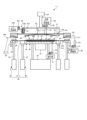
本発明の実施形態1に係るエキスパンド装置を図面に基づいて説明する。図1は、実施形態1に係るエキスパンド装置の加工対象の被加工物ユニットの一例を示す斜視図である。図2は、実施形態1に係るエキスパンド装置の構成例を模式的に示す断面図である。図3は、図2に示されたエキスパンド装置の湾曲プレート等を模式的に示す断面図である。
本発明の実施形態1の変形例に係るエキスパンド装置を図面に基づいて説明する。図8は、実施形態1の変形例に係るエキスパンド装置の構成例を模式的に示す断面図である。なお、図8は、実施形態1と同一部分に同一符号を付して説明を省略する。
20 フレーム保持ユニット(フレーム保持手段)
30 冷却テーブル
31 当接面
40 拡張ユニット(拡張手段)
50 加熱ユニット(加熱手段)
52 温風噴射部
90 湾曲プレート(温風進入防止手段)
91 噴出口
92 湾曲面
200 被加工物ユニット
201 被加工物
210 エキスパンドシート
211 環状フレーム
300 温風
301 空気溜まり
Claims (3)
- 被加工物と、被加工物に貼着されたエキスパンドシートと、エキスパンドシートの外周側が貼着された環状フレームと、からなる被加工物ユニットの該エキスパンドシートを拡張するエキスパンド装置であって、
被加工物ユニットの環状フレームを保持するフレーム保持手段と、
被加工物に対応した大きさの当接面を含み、該フレーム保持手段で保持された該環状フレームを含む該被加工物ユニットの該エキスパンドシートに当接する冷却テーブルと、
該フレーム保持手段で保持された該環状フレームに貼着された該エキスパンドシートを拡張する拡張手段と、
被加工物の外周側と該環状フレームの内周縁との間の該エキスパンドシートに対面して温風を噴射する温風噴射部を有した加熱手段と、
被加工物と該温風噴射部との間に配設され、該被加工物に向かって気体を噴出する噴出口を有し、該温風噴射部から噴射された温風の進入を防止する温風進入防止手段と、
該冷却テーブルの外周を覆い、かつ該加熱手段が該被加工物の外周側と該環状フレームの内周縁との間の該エキスパンドシートに温風を噴射する際に、該冷却テーブルとの間から圧縮エアーを吹き出すテーブルカバーと、
を備えたエキスパンド装置。 - 該冷却テーブルが該被加工物と該エキスパンドシートとの間の接着フィルムを冷却しながら該拡張手段が該エキスパンドシートを拡張する際に、
該テーブルカバーは、該冷却テーブルとの間から該圧縮エアーを吹き出し、かつ、該フレーム保持手段は、全周に亘って設けられた吹き出し口から圧縮エアーを吹き出す、請求項1に記載のエキスパンド装置。 - 該温風進入防止手段は、被加工物に対面し、該当接面に対応したサイズに形成された、被加工物の外周側より中央側において被加工物との間の距離が遠くなるよう反りを有した湾曲面を含み、該湾曲面に該噴出口が形成されることで該湾曲面と被加工物の間に空気溜まりを形成する、請求項1又は請求項2に記載のエキスパンド装置。
Priority Applications (4)
| Application Number | Priority Date | Filing Date | Title |
|---|---|---|---|
| JP2019148838A JP7325258B2 (ja) | 2019-08-14 | 2019-08-14 | エキスパンド装置 |
| KR1020200086503A KR20210020766A (ko) | 2019-08-14 | 2020-07-14 | 익스펜드 장치 |
| TW109127062A TW202107624A (zh) | 2019-08-14 | 2020-08-10 | 擴片裝置 |
| CN202010799432.9A CN112397416A (zh) | 2019-08-14 | 2020-08-11 | 扩展装置 |
Applications Claiming Priority (1)
| Application Number | Priority Date | Filing Date | Title |
|---|---|---|---|
| JP2019148838A JP7325258B2 (ja) | 2019-08-14 | 2019-08-14 | エキスパンド装置 |
Publications (2)
| Publication Number | Publication Date |
|---|---|
| JP2021034397A JP2021034397A (ja) | 2021-03-01 |
| JP7325258B2 true JP7325258B2 (ja) | 2023-08-14 |
Family
ID=74603831
Family Applications (1)
| Application Number | Title | Priority Date | Filing Date |
|---|---|---|---|
| JP2019148838A Active JP7325258B2 (ja) | 2019-08-14 | 2019-08-14 | エキスパンド装置 |
Country Status (4)
| Country | Link |
|---|---|
| JP (1) | JP7325258B2 (ja) |
| KR (1) | KR20210020766A (ja) |
| CN (1) | CN112397416A (ja) |
| TW (1) | TW202107624A (ja) |
Families Citing this family (2)
| Publication number | Priority date | Publication date | Assignee | Title |
|---|---|---|---|---|
| KR20230081644A (ko) | 2021-11-30 | 2023-06-07 | 가부시기가이샤 디스코 | 익스팬드 장치 |
| KR20230100060A (ko) | 2021-12-28 | 2023-07-05 | 세메스 주식회사 | 다이 사이의 간격을 확장하기 위한 웨이퍼 익스팬더, 및 이를 포함하는 다이 공급 모듈 및 다이 본딩 설비 |
Citations (4)
| Publication number | Priority date | Publication date | Assignee | Title |
|---|---|---|---|---|
| JP2009224775A (ja) | 2008-02-20 | 2009-10-01 | Tokyo Electron Ltd | ガス供給装置、成膜装置及び成膜方法 |
| JP2013051368A (ja) | 2011-08-31 | 2013-03-14 | Tokyo Seimitsu Co Ltd | ワーク分割装置及びワーク分割方法 |
| JP2019067945A (ja) | 2017-10-02 | 2019-04-25 | 株式会社ディスコ | テープ拡張装置及びテープ拡張方法 |
| JP2019110268A (ja) | 2017-12-20 | 2019-07-04 | 株式会社ディスコ | 分割装置 |
Family Cites Families (2)
| Publication number | Priority date | Publication date | Assignee | Title |
|---|---|---|---|---|
| EP1608201A1 (en) | 2004-06-15 | 2005-12-21 | Alcatel | Positioning of network processor in a packet based access multiplexer |
| KR20110077482A (ko) | 2009-12-30 | 2011-07-07 | 이유에스티(주) | 이피트리 데이터가 저장된 알에프아이디를 통한 기부자와 수혜자의 데이터관리 시스템 및 방법 |
-
2019
- 2019-08-14 JP JP2019148838A patent/JP7325258B2/ja active Active
-
2020
- 2020-07-14 KR KR1020200086503A patent/KR20210020766A/ko active Search and Examination
- 2020-08-10 TW TW109127062A patent/TW202107624A/zh unknown
- 2020-08-11 CN CN202010799432.9A patent/CN112397416A/zh active Pending
Patent Citations (4)
| Publication number | Priority date | Publication date | Assignee | Title |
|---|---|---|---|---|
| JP2009224775A (ja) | 2008-02-20 | 2009-10-01 | Tokyo Electron Ltd | ガス供給装置、成膜装置及び成膜方法 |
| JP2013051368A (ja) | 2011-08-31 | 2013-03-14 | Tokyo Seimitsu Co Ltd | ワーク分割装置及びワーク分割方法 |
| JP2019067945A (ja) | 2017-10-02 | 2019-04-25 | 株式会社ディスコ | テープ拡張装置及びテープ拡張方法 |
| JP2019110268A (ja) | 2017-12-20 | 2019-07-04 | 株式会社ディスコ | 分割装置 |
Also Published As
| Publication number | Publication date |
|---|---|
| TW202107624A (zh) | 2021-02-16 |
| JP2021034397A (ja) | 2021-03-01 |
| KR20210020766A (ko) | 2021-02-24 |
| CN112397416A (zh) | 2021-02-23 |
Similar Documents
| Publication | Publication Date | Title |
|---|---|---|
| JP7325258B2 (ja) | エキスパンド装置 | |
| JP2011077482A (ja) | テープ拡張装置 | |
| CN107039261B (zh) | 分割装置以及晶片的分割方法 | |
| JP5885033B2 (ja) | ワーク分割装置及びワーク分割方法 | |
| JP7030469B2 (ja) | テープ拡張装置及びテープ拡張方法 | |
| JP6298635B2 (ja) | 分割装置及び被加工物の分割方法 | |
| CN109860110B (zh) | 晶片的分割方法和晶片的分割装置 | |
| KR20150128579A (ko) | 칩 간격 유지 장치 및 칩 간격 유지 방법 | |
| JP6494360B2 (ja) | 拡張装置 | |
| JP7076204B2 (ja) | 分割装置 | |
| JP7437963B2 (ja) | エキスパンド装置 | |
| TW201828347A (zh) | 分割裝置及分割方法 | |
| JP4971869B2 (ja) | 接着フィルム破断装置 | |
| TWI826641B (zh) | 擴展裝置 | |
| JP2023081298A (ja) | エキスパンド装置 | |
| TW202324520A (zh) | 擴展裝置 | |
| JP2010027666A (ja) | 破断方法及び破断装置 | |
| JP2017050573A (ja) | ワーク分割装置 | |
| JP5939416B2 (ja) | ワーク分割装置及びワーク分割方法 | |
| KR20200121229A (ko) | 익스팬드 장치, 익스팬드 방법 | |
| JP2024061394A (ja) | 拡張方法及び拡張装置 | |
| JP7345328B2 (ja) | 被加工物の加工方法 | |
| JP6955927B2 (ja) | 接着フィルムの破断装置及び接着フィルムの破断方法 | |
| TW202221778A (zh) | 擴展裝置及擴展方法 | |
| JP6060475B2 (ja) | ワーク分割装置及びワーク分割方法 |
Legal Events
| Date | Code | Title | Description |
|---|---|---|---|
| A621 | Written request for application examination |
Free format text: JAPANESE INTERMEDIATE CODE: A621 Effective date: 20220617 |
|
| A131 | Notification of reasons for refusal |
Free format text: JAPANESE INTERMEDIATE CODE: A131 Effective date: 20230516 |
|
| A977 | Report on retrieval |
Free format text: JAPANESE INTERMEDIATE CODE: A971007 Effective date: 20230518 |
|
| A521 | Request for written amendment filed |
Free format text: JAPANESE INTERMEDIATE CODE: A523 Effective date: 20230704 |
|
| TRDD | Decision of grant or rejection written | ||
| A01 | Written decision to grant a patent or to grant a registration (utility model) |
Free format text: JAPANESE INTERMEDIATE CODE: A01 Effective date: 20230718 |
|
| A61 | First payment of annual fees (during grant procedure) |
Free format text: JAPANESE INTERMEDIATE CODE: A61 Effective date: 20230801 |
|
| R150 | Certificate of patent or registration of utility model |
Ref document number: 7325258 Country of ref document: JP Free format text: JAPANESE INTERMEDIATE CODE: R150 |